31
Chapter 1 1 Electrons in periodic potential • Energy gap – nearly free electron • Bloch Theorem • Energy gap – tight binding Three Most Important Topics (MIT) Today

Chapter 1 1
Electrons in periodic potential• Energy gap – nearly free electron• Bloch Theorem• Energy gap – tight binding
Three Most Important Topics (MIT) Today

Chapter 1 2
•We now know the crystal structure, Bravais lattice, and reciprocal lattice.
•The reciprocal lattice had a context derived from diffraction – a wave effect
•We now extend this to understand how electrons will behave in periodic potential of our the crystal
•Because this is a wave problem in periodic potential , a good way of understanding this is through the k-space rather than the real space.
Electrons in Periodic Potential
22 ( ) ( ) ( ) ( ) ; ( ) ( )
2r V r r E r V r V r T
mψ ψ ψ− ∇ + = = +
h

Chapter 1 3
Energy Gap – Near Free Electron Model V~0At Bragg planes, for a one-dimensional lattice
2( ) ( )2 2
; '2 2
G Gk G k
G n G nk ka aπ π
Δ = ⋅ =
⇒ = = = − = −
eikx eik’x
2 2
2 2
( ) exp( / ) exp( / ) 2cos( / )( ) exp( / ) exp( / ) 2 sin( / )( ) | ( ) | cos ( / )( ) | ( ) | sin ( / )
i x a i x a x ai x a i x a i x a
n x an x a
ψ π π πψ π π π
ψ π
ψ π
+ = + − =− = − − =
+ = + ∝
− = − ∝
0 2π/aAt k=π/a
π/ak
Bragg Plane
The different charge distribution causes variation of the electrostatic potential energy in the field of the positive ion cores

Chapter 1 4
Energy Gap – Near Free Electron Model
Kittel Fig 7-3

Chapter 1 5
Energy Gap – Near Free Electron Model
Kittel Fig 7-2

Chapter 1 6
We know n(r+T) =n(r) → |Ψnk(r+T)|2= |Ψnk(r)|2
Bloch Theorem
The solution of Schrodinger equation for a periodic potential:2
2 ( ) ( ) ( ) ( ) ; ( ) ( )2
r V r r E r V r V r Tm
ψ ψ ψ− ∇ + = = +h
( ) ( ) or
( ) e ( ) with ( ) ( )
ikTnk nk
ikrnk nk nk nk
r T e r
r u r u r u r T
ψ ψ
ψ
∴ + =
= = +
Periodic function coming from the influence of the lattice potential.
Modulated plane waveProbability of finding electronis not constant anymore.The general proof of the Bloch Theorem can be done by expanding V(r) and Ψ (r) into a Fourier series and then rewriting the Schrödinger equation.
n and k are two quantum numbers in S.E. k is the wave vector index and n is called band index.

Chapter 1 7
Implication of Bloch Theorem• The Bloch theorem is quite remarkable, because, as said before, it
imposes very special conditions on any solution of the Schrödinger equation, no matter what the form of the periodic potential might be.
• The quantity k, while still being the index of multiple solutions and the wave vector of the plane wave that is part of the wave function (and which may be seen as the "backbone" of the Bloch functions), has lost its simple meaning: It can no longer be taken as a direct representation of the momentum p of the wave via p = Һ k. The proof could be seen by imposing the momentum operator on the Bloch function and understand that the Bloch function is no longer themomentum eigenstate (Hamiltonian and momentum operators are not commutable).
• The momentum of the electron moving in a periodic potential is no longer constant ; for the standing waves resulting from reflections at the Brillouin zones boundary it is actually zero (because the velocity is zero), while k is not.

Chapter 1 8
Implication of Bloch Theorem• Instead of associating k with the momentum of the electron, we may
identify the quantity k, which is obviously still a constant, with the so-called crystal momentum P, something like the combined momentum of crystal and electron.
• The crystal momentum P, while not a "true" momentum, still has many properties of momentums, in particular it is conserved during all kinds of processes and obey the relationship of Һ (dk/dt)=-eF under the influence of external field.
• The index n represents the fact that there are multiple solutions to S.E for given k.
put it back to S.E.
similar to the “particle in a box” problem, you are going to find multiple solutions of uk(r) which we label with the band index n.
( ) e ( ) ikrk kr u rψ =
( ) = ( ) with B.C. ( ) ( )k k k k k kH u r E u r u r u r T= +

Chapter 1 9
Reduced Zone Scheme
Assume we know a Bloch function with k’ lies outside the 1st BrillouinZone, we can always find a reciprocal lattice vector G such that k = k’ + G lies within the 1st B.Z.
'' ' '
' '
' '
( ) e ( ) = e ( ( ))
e ( ) ( )
ik r ikr iGrnk nk nk
ikrn k n k
nk n k
r u r e u r
u r rE E
ψ
ψ
−=
≡ =
∴ =
Periodic in T
This is a significant result that allows any wave vector k’ outside of the 1st B.Z. can be represented by a wave vector k, differed by G, in the 1st
B.Z but with different band index n, i.e. Enk’≠ Enk

Chapter 1 10
k
E
band n0π/a 2π/a-2π/a -π/a
Extend Zone Scheme
Reduced Zone Scheme
k
E
π/a 2π/a-2π/a -π/a
Reduced Zone Scheme
1st B.Z.
band n0
band n1
band n2

Chapter 1 11
• Atom can be approximated with “the core” and “the valence electrons” (similar to the “pseudo-potential” approximation: The core is the nucleus and the filled states of electrons with the same major quantum number n, such as 1S2, 2S2, 2P6, etc...
• Valence electrons are:– outermost electrons in orbital concepts– easiest to break off from the nucleus– participate in the chemical reactions– can break the Coulombic potential (ionization) and contribute to
conduction– dominant in chemical and semiconductor discussions (why the
periodic table is very important)
Orbit Model: Connection to Chemistry

Chapter 1 12
Strongest bond with anti-parallel spin and Pauli Exclusion Principle’s modification of charge distribution through spin-dependent Coulomb energy
Covalent Bonds: H2ψA
ψB
Kittel, p.73
ψA+ ψB ψA- ψB
Wavefunction overlap controls the formation of the bonding and antibonding states.
EA EA
bonding
antibonding

Chapter 1 13
Tight Binding Approach for Energy Bands
Two atoms are brought together, two separated energy levels are formed for each level of the isolated atom. For N atoms, N levels (bands) are formed for each level of the isolated atom. (Pauli exclusion)
The bandwidth of each band is determined by the wavefunction overlap. Larger overlap (shorter nearest neighbor distance), larger bandwidth.

Chapter 1 14
Semiconductor Band Structure
Indirect bandgap direct bandgap
Band Structure: The unique electron momentum and energy relation (E-k dispersion) of particular materials including the periodic potential disturbance from the ion cores (QM problem).

Chapter 1 15
1st BZ for Diamond/Zincblende Lattice
Pierret Fig. 3-12
Γ: Zone center (k=0)X : Zone boundary along <100> directionL : Zone boundary along <111> direction

Chapter 1 16
E-k Relationship – Effective Mass
2 2
0 *
2
* 2 2
( )2
1 1
1g
kE k Em
d Em dk
d d Evdk dkω
= +
=
= =
h
h
h
k
E Zone Boundary
G/2
1st band
2nd bandFree electron
Near the band maximum (minimum), the E-k relation can be approximated by the parabolic dispersion:
Curvature of the parabola
In semiconductors, m* is usually smaller than m0 (free electron mass) due to the larger curvature at the band extreme.Effective mass is even a simpler concept than the band structure. Together with the concept of the bandgap, classical mechanisms can be applied to describe the electron motion in the solid without dealing with QM !!
m1*
m2*
m1* >m2
* Slope of the parabola

Chapter 1 17
Constant Energy Surface2 22 2 2 2
31 20 * * *
1 2 3
( )2 2 2
kk kE k Em m m
= + + +hh h

Chapter 1 18
Constant Energy Surface
6 ellipsoids

Chapter 1 19
Electron and Hole
• The hole is an alternative description of a band with one missing electron.
• The motion for a hole is that of a particle of positive charge e.
k
E
k
EF
k
EF
ve je
jh
vhF

Chapter 1 20
Density of States (Particle in the 3D Box)
EC=0
ETOP
ECEV
2 2 2 2 22
2 2 2
22
2
( ) ( ) ( ) ( )2 2
Assume ( ) ( ) ( ) ( ) ;
( ) ( )2
B.C. ( ) ( ) Circular B.C.(See Kittel for periodic B.C.)
2 4 6where 0, , ,x
x y z x y z
xx x
x x
ik xx x
r r E rm m x y z
r x y z E E E E
d x E xm dx
x x L
e kL L
ψ ψ ψ
ψ ψ ψ ψ
ψ ψ
ψ ψ
π πψ
∂ ∂ ∂− ∇ = − + + =
∂ ∂ ∂= = + +
− =
= +
⇒ = = ± ± ±
h h
h
2 2 2 2 2
( )
2 /
yx zik yik x ik z
x y z
Lr Ae e e
k mE k k k
π
ψ⇒ =
= = + +
K
h
∞
x=0 x=L

Chapter 1 21
3
3 23 1/3
3 2
2 2 2 22/3 3/2
2 2
2 4 3From above: , , 0, , ,
2one allowed state per volume of ( ) in k space
(4 / 3) 3total state ( ) 2 ( )(2 / ) 3
3 2 ( ) ( ) ( )2 2 3
The number of st
x y zk k kL L L
Lk V NN k k k
L Vk N V mE Nm m V
π π π
π
π ππ π
π εεπ
= ± ± ±
∴
= ⋅ = ⇒ =
= = ⇒ =
K
h h
h
2 3
ates per volume per unit energy or
2Density of States (DOS) ( ) dN m mEg EdEdV π
= =h
Density of States (Particle in the 3D Box)
kx
ky
kz
k
DOS is zero at the band edge in QM sense.g(E)dE is the available states from E to E + dE, not the carrier concentration yet!
g(E)
E
~E1/2
Chapter 1 22
Density of States in Specific Material
In the real material considering the periodic potential, the derivation of the DOS is much more complicate.But at the band extreme, it can be approximated by the similar parabolic relation with correction on the electron effective mass.
* *
2 3
* *
2 3
2 ( )( )
2 ( )( )
n n cc c
p p vv v
m m E Eg E E E
m m E Eg E E E
π
π
−= ≥
−= ≤
h
h
conduction band
valence band

Chapter 1 23
• How S states is filled by N electrons?– The carrier distribution will be described by the Fermi
functions (both electrons and holes are Fermions. In contrast, photons and phonons are Bosons). This describes the number of carriers in a specific energy level.
– Given the Fermi energy EF of the system (EF is a constant in equilibrium), the Fermi distribution function with respect to the energy of a single-particle state E is:
TkEE BFeEf /)(1
1)( −+= Derived from statistic mechanics
and thermodynamics
Fermi Distribution (Occupancy of States)

Chapter 1 24
– if E >> EF , f(E) ∝ exp( (EF - E)/kBT ), which is the Boltzmann distribution for electrons
– if E << EF , f(E) ≈ 1 - exp(- (EF - E)/kBT ) or holes forexp( -(EF - E)/kBT ),
– if E = EF , f(E) = 0.5
f(E)
EF
f(E)
EF
T=0 T>0
TkEE BFeEf /)(1
1)( −+=
0.50.5
The Fermi Function
Below EF: occupied Above EF: empty

Chapter 1 25
• Insulator (in room temperature) : Egap > 4eV (SiO2: 9.1eV, Si3N4: ~5eV)
• Conductor: Egap < 3 kT ~ 0.1eV, or even negative bandgap• Semiconductor: anything in between, depending on what
temperature we are talking about.• Regular semiconductor in room temperature: Si: Egap= 1.12
eV; Ge: Egap= 0.66eV and GaAs: Egap= 1.42 eV: this is the system that can be dealt with most easily.
• For wide-bandgap materials (Egap~ 2-3eV), conduction is usually governed more by the structural imperfection
• For narrow-bandgap materials (Egap~ 0.25eV), conduction is usually governed by DOS of available states.
Material Characterization by Bandgap

Chapter 1 26
Material Characterization by Bandgap
Metal Semi-metal Semiconductor Insulator
Chapter 1 27
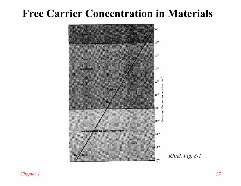
Free Carrier Concentration in Materials
Kittel, Fig. 8-1

Chapter 1 28
Intrinsic case (electrical properties of “pure” semiconductor)– All conduction caused by thermal breakup of electron-hole pairs– n=p=ni, 1.4×1010 cm-3 for Si, 2×10⁶ for GaAs, and 2×10¹³ for Ge at 300K– There are about 5 × 10²² atoms/cm3, and 2 × 10²³ valence electrons– Because the energy for generating electron-hole pairs is from the thermal
energy, ni increases exponentially with temperature.
Intrinsic Semiconductors

Chapter 1 29
N-type Semiconductors
Charge species: n and ND+ and n ≅ ND
+ in bulk N-type semiconductors for charge neutrality.

Chapter 1 30
P-type Semiconductors
Charge species: p and NA− and p ≅ NA
− in bulk N-type semiconductors for charge neutrality.

Chapter 1 31
• Use of doping (impurity) to create conduction carriers more easily– The Bohr model: EB = q4m*/2(4πεsε0h)2 ≈Ehm*/m0εs
2≈0.1eV– This is because the carrier looks at the ionized impurity
through the sea of other Si atoms and valence band, and the bond strength needs to be corrected with the dielectric constant (polarization effect) and the effective mass (periodic potential)
– There is solid solubility limit depending on temperature. Above the limit, the dopants will form segregates.
N-type EB(eV) P-type EB (eV)Donors AcceptorsP 0.045 B 0.045As 0.054 Al 0.067Sb 0.039 Ga 0.072
In 0.16
Doping in Semiconductors
Ionization energy of hydrogen
![PERIODIC CLASSIFICATION & PERIODIC PROPERTIES [ 1 ...youvaacademy.com/youvaadmin/image/PERIODIC TABLE BY RS.pdf · [ 2 ] PERIODIC CLASSIFICATION & PERIODIC PROPERTIES BY RAJESH SHAH](https://static.documents.pub/doc/80x56/604570870a43592d4f6b3e29/periodic-classification-periodic-properties-1-table-by-rspdf-2.jpg)


