Flash for wearables Electroplating An old technology for the future AIM image MEMS devices Smaller & more stable memory Antennas on a computer chip Beyond the lithium ion Features, News Review, Industry Analysis, Research News and much more. Free Weekly E News round up , go to www.siliconsemiconductor.net Volume 37 Issue II 2015 @siliconsemi www.siliconsemiconductor.net
Transcript
Flash for wearables
ElectroplatingAn old technology
for the future
AIM image MEMS devices
Smaller & more stable memory
Antennas on a computer chip
Beyond the lithium ion
Features, News Review, Industry Analysis, Research News and much more.
Free Weekly E News round up , go to www.siliconsemiconductor.net
Volume 37 Issue II 2015 @siliconsemi www.siliconsemiconductor.net
22 www.siliconsemiconductor.net Issue II 2015
COVER STORY
Issue II 2015 www.siliconsemiconductor.net 23
COVER STORY
ElectroplatingAn old technology for the future
ALTHOUGH IT MAY SEEM counterintuitive, a great many of the industry’s most advanced devices, such as compound semiconductors, MEMs and smart sensors that are used in the latest electronics applications, are not built using the most advanced process technology on the largest wafers. There are a couple of reasons for this. In many cases, such as analog devices, the desired level of functionality can be achieved using 90 nm or larger critical dimensions rather than today’s leading-edge 14 nm standard. In others, it can be cost. It makes no sense to invest in a 300 mm process line if market demand can be met using 200 mm wafers.
While large semiconductor manufacturers, especially those producing large volumes of logic or memory devices, have adopted the latest in metal deposition technology, many others have found that time-tested methods of depositing metal onto substrates — such as sputtering and evaporation — have cost-effectively met their requirements. That is changing. As technologies such as wafer-level packaging are increasingly adopted, these useful and relatively inexpensive techniques are reaching their limits. This article will briefly describe some of these limitations and suggest a proven alternative that can overcome them.
Capability limitsSputtering and evaporation are limited in three main areas when it comes to wafer-level packaging applications: poor step coverage; limited feature fill; and poor metal lift-off for small features. Sputtering, for example, is mostly a
line-of-sight process that relies on probability and randomness to uniformly deposit the desired thickness of metal on the substrate. High-aspect features, such as deep vias, the thick resist used for copper pillars, or the narrowly spaced lines found in redistribution layers cannot be properly filled. For structures that span different elevations within a die, it can be virtually impossible to achieve greater than 20-30 percent step coverage, even if continuity can be maintained. At the same time, once aspect ratios increase much beyond 3:1, filling features with metal, whether
Kevin Witt, ClassOne Technology Vice President, offers insight into ways that classic electroplating processes are being updated to address the industry’s latest metal deposition requirements.
24 www.siliconsemiconductor.net Issue II 2015
COVER STORY
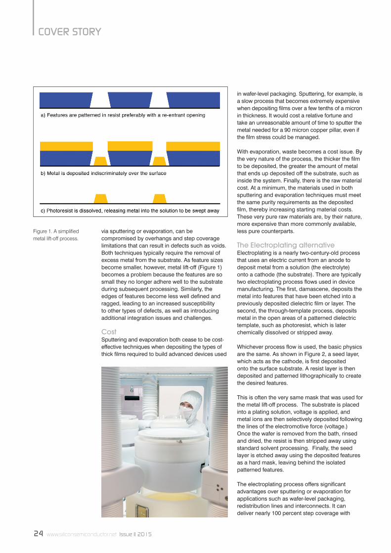
via sputtering or evaporation, can be compromised by overhangs and step coverage limitations that can result in defects such as voids. Both techniques typically require the removal of excess metal from the substrate. As feature sizes become smaller, however, metal lift-off (Figure 1) becomes a problem because the features are so small they no longer adhere well to the substrate during subsequent processing. Similarly, the edges of features become less well defined and ragged, leading to an increased susceptibility to other types of defects, as well as introducing additional integration issues and challenges.
Cost Sputtering and evaporation both cease to be cost-effective techniques when depositing the types of thick films required to build advanced devices used
in wafer-level packaging. Sputtering, for example, is a slow process that becomes extremely expensive when depositing films over a few tenths of a micron in thickness. It would cost a relative fortune and take an unreasonable amount of time to sputter the metal needed for a 90 micron copper pillar, even if the film stress could be managed.
With evaporation, waste becomes a cost issue. By the very nature of the process, the thicker the film to be deposited, the greater the amount of metal that ends up deposited off the substrate, such as inside the system. Finally, there is the raw material cost. At a minimum, the materials used in both sputtering and evaporation techniques must meet the same purity requirements as the deposited film, thereby increasing starting material costs. These very pure raw materials are, by their nature, more expensive than more commonly available, less pure counterparts.
The Electroplating alternative Electroplating is a nearly two-century-old process that uses an electric current from an anode to deposit metal from a solution (the electrolyte) onto a cathode (the substrate). There are typically two electroplating process flows used in device manufacturing. The first, damascene, deposits the metal into features that have been etched into a previously deposited dielectric film or layer. The second, the through-template process, deposits metal in the open areas of a patterned dielectric template, such as photoresist, which is later chemically dissolved or stripped away.
Whichever process flow is used, the basic physics are the same. As shown in Figure 2, a seed layer, which acts as the cathode, is first deposited onto the surface substrate. A resist layer is then deposited and patterned lithographically to create the desired features.
This is often the very same mask that was used for the metal lift-off process. The substrate is placed into a plating solution, voltage is applied, and metal ions are then selectively deposited following the lines of the electromotive force (voltage.) Once the wafer is removed from the bath, rinsed and dried, the resist is then stripped away using standard solvent processing. Finally, the seed layer is etched away using the deposited features as a hard mask, leaving behind the isolated patterned features.
The electroplating process offers significant advantages over sputtering or evaporation for applications such as wafer-level packaging, redistribution lines and interconnects. It can deliver nearly 100 percent step coverage with
Figure 1. A simplified metal lift-off process.
26 www.siliconsemiconductor.net Issue II 2015
COVER STORY
excellent feature fill, minimizing defect and integration issues. A simple, self-organizing process, it also offers deposition rates in excess of 4 microns per minute for some materials, making it an excellent technique for depositing the thick films required to build features such as the 90 micron copper pillars mentioned above. Its faster deposition rate also speeds wafer throughput and lowers overall cost of ownership. Electroplating offers an additional benefit since it is a purification process by nature. As a result, the raw materials need not be of the same level of purity required for sputtering or evaporation, which further lowers production costs. Finally, electroplating offers a much wider process window than the alternative processes, thereby increasing process flexibility.
As many university students have learned, making and using a small electroplating cell is simple and inexpensive. Outside of the laboratory and in the fab environment, the use of automated equipment and hazardous chemicals introduces concerns that need to be mitigated. There have been many different types of electroplating systems put into service over the years with varying degrees of success. Like most processes in semiconductor device manufacturing, electroplating makes
use of potentially dangerous chemicals, so safety is a concern. Exposed or open baths of electroplating chemicals can be risky to both operations and maintenance personnel, as well as to the equipment itself. Chemicals can also pose environmental and facility contamination risks. Care should always be taken to ensure that plating equipment has integrated secondary containment and appropriate fail-safes as well as interlocks, such as those called for in the SEMI S2, CE, or FM4910 specifications. Since plating solutions tend to be corrosive, material compatibility becomes an important issue for safety as well as for maximizing asset longevity.
Once safety guidelines and process controls are taken into consideration, choosing a plating system comes down to the performance to price ratio for the production volumes in question. Wet benches are often used for non-critical plating operations and can be either automated or manually operated, depending on production needs. For low levels of non-critical production, the variability in results that arise from manually operated equipment may not become an issue. Alternately, hand operations can become cumbersome as volume levels increase. When reproducibility and its consequent variation reduction matters, or when a high degree of uniformity is demanded, wet benches fall short and single wafer tools are desirable.
Single wafer tools fall into two general categories: fountain platers and paddle platers. Used more widely in the industry, fountain platers place a wafer face down into an overflowing pool while the wafer rotates. By comparison, paddle platers mechanically agitate the electrolyte near the surface of a static wafer. Paddle platers often can achieve higher ultimate plating rates for the same chemistry (due to a higher amount of agitation). But this benefit needs to be considered against the mechanical complexity of the chamber and necessary automation, which lead to increased costs. These tools tend to be physically larger than their fountain plater counterparts, which may be a concern for older, more space-constrained facilities.
Figure 2. A simplified electroplating process.
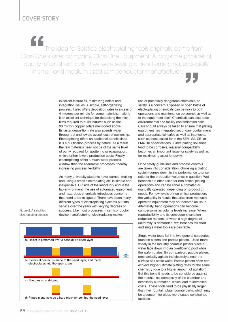
“The idea for Solstice electroplating tools originally came from ClassOne’s sister company, ClassOne Equipment. A long-time provider of quality refurbished tools, they were seeing a trend emerging, especially
in small and medium-sized semiconductor manufacturers
”
Issue II 2015 www.siliconsemiconductor.net 27
COVER STORY
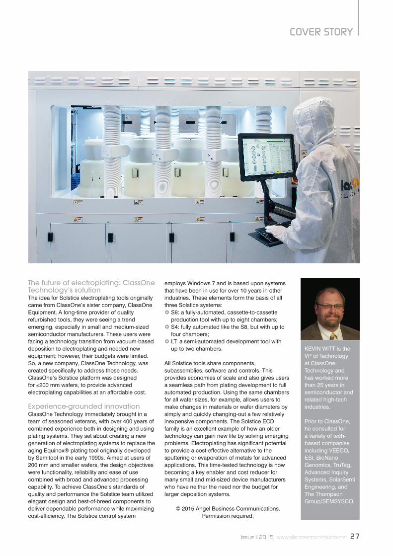
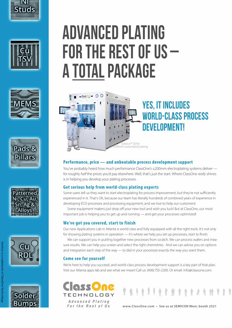
The future of electroplating: ClassOne Technology’s solution The idea for Solstice electroplating tools originally came from ClassOne’s sister company, ClassOne Equipment. A long-time provider of quality refurbished tools, they were seeing a trend emerging, especially in small and medium-sized semiconductor manufacturers. These users were facing a technology transition from vacuum-based deposition to electroplating and needed new equipment; however, their budgets were limited. So, a new company, ClassOne Technology, was created specifically to address those needs. ClassOne’s Solstice platform was designed for ≤200 mm wafers, to provide advanced electroplating capabilities at an affordable cost.
Experience-grounded innovationClassOne Technology immediately brought in a team of seasoned veterans, with over 400 years of combined experience both in designing and using plating systems. They set about creating a new generation of electroplating systems to replace the aging Equinox® plating tool originally developed by Semitool in the early 1990s. Aimed at users of 200 mm and smaller wafers, the design objectives were functionality, reliability and ease of use combined with broad and advanced processing capability. To achieve ClassOne’s standards of quality and performance the Solstice team utilized elegant design and best-of-breed components to deliver dependable performance while maximizing cost-efficiency. The Solstice control system
employs Windows 7 and is based upon systems that have been in use for over 10 years in other industries. These elements form the basis of all three Solstice systems: £ S8: a fully-automated, cassette-to-cassette production tool with up to eight chambers; £ S4: fully automated like the S8, but with up to four chambers;£ LT: a semi-automated development tool with up to two chambers.
All Solstice tools share components, subassemblies, software and controls. This provides economies of scale and also gives users a seamless path from plating development to full automated production. Using the same chambers for all wafer sizes, for example, allows users to make changes in materials or wafer diameters by simply and quickly changing-out a few relatively inexpensive components. The Solstice ECD family is an excellent example of how an older technology can gain new life by solving emerging problems. Electroplating has significant potential to provide a cost-effective alternative to the sputtering or evaporation of metals for advanced applications. This time-tested technology is now becoming a key enabler and cost reducer for many small and mid-sized device manufacturers who have neither the need nor the budget for larger deposition systems.
KEVIN WITT is the VP of Technology at ClassOne Technology and has worked more than 25 years in semiconductor and related high-tech industries.
Prior to ClassOne, he consulted for a variety of tech-based companies including VEECO, ESI, BioNano Genomics, TruTag, Advanced Inquiry Systems, SolarSemi Engineering, and The Thompson Group/SEMSYSCO.
A d v a n c e d P l a t i n gF o r t h e R e s t o f U s
You’ve probably heard how much performance ClassOne’s ≤200mm electroplating systems deliver — for roughly half the prices you’d pay elsewhere. Well, that’s just the start. Where ClassOne really shines is in helping you develop your plating processes.
Performance, price — and unbeatable process development support
Get serious help from world-class plating expertsSome users tell us they want to start electroplating for process improvement, but they’re not su� ciently experienced in it. That’s OK, because our team has literally hundreds of combined years of experience in developing ECD processes and processing equipment; and we love to help our customers! Some equipment makers just drop o� your new tool and wish you luck! But at ClassOne, our most important job is helping you to get up and running — and get your processes optimized!
Come see for yourselfWe’re here to help you succeed, and world-class process development support is a key part of that plan. Visit our Atlanta apps lab and see what we mean! Call us: (406) 755-2200. Or email: [email protected].
ADVANCED PLATING FOR THE REST OF US –A TOTAL PACKAGE
www.ClassOne.com • See us at SEMICON West, booth 2521
We’ve got you covered, start to finishOur new Applications Lab in Atlanta is world class and fully equipped with all the right tools. It’s not only for showing plating systems in operation — it’s where we help you set up processes, start to � nish. We can support you in putting together new processes from scratch. We can process wafers and mea-sure results. We can help you screen and select the right chemistries. And we can advise you on options and integration each step of the way — to dial in your processes exactly the way you want them.