ELSEVIER Sensors and Actuators A 45 (1994) 57-66 PHYSICAL Electrostatically driven vacuum-encapsulated polysilicon resonators Part I. Design and fabrication Rob Lqtenberg, Harrie A.C. Tilmans* MES4 Research Institute, Vnive@v of Twente, PO Box 21% NL-7500 AE Enschedz, Netherlands Received 1 July 1993; accepted in revised form 2 June 1994 Abstract Basic design issues and a fabrication process based on surface-micromachining‘techniques for electrostatically driven vacuum- encapsulated polysilicon resonators are presented. A novel freeze-drying method that does not require vacuum equipment is presented. Reactive sealing with LPCVD silicon nitride is used to create the evacuated cavity, resulting in cavity pressures close to the deposition pressure. Design issues regarding choice of materials, technology and layout are discussed, First experimental results, including an admittance plot of the one-port resonator and a plot indicating the dependence of the Q- factor on the resonator geometry and ambient pressure, are presented. I(eywordF: Electrostatic excitation and detection; Surface-micromachining techniques; Polysiliwn resonators; Vacuum encapsulation 1. Introduction Resonant sensors are very attractive for the precise measurement of mechanical quantities such as pressure and force. They offer high sensitivity and resolution together with a semidigital output, i.e., a frequency [l-4]. The central part of the sensor is a vibrating mechanical element called the resonator, which provides the frequency (shift) output. Surface-micromachined resonators that are operated in a flexural mode of vibration have been used by several research groups in the past [S-7]. Without taking special precautions, these resonators suffer from small signal responses as a result of a low mechanical quality factor. The low quality factor is a direct consequence of the introduction of a second surface in close proximity to the resonator surface. This leads to so-called squeeze- film damping, which can be observed for the normal vibrational motion of two closely spaced surfaces [.5,8]. Squeeze-film damping becomes significant if the gap spacing is small compared to the lateral dimensions of the resonator. Evacuating the surroundings would elim- *Present address: Katholieke Universiteit Leuven, Departement Elektrotechniek-ESAT, Kardiiaal Mercierlaan 94, B-3001 Heverlee, Belgium. inate this effect. At the same time, unwanted envi- ronmental effects, such as changes in the density of the surrounding medium, humidity and dust, are elim- inated as well. Thus, the resonator must be placed inside a vacuum housing. This was realized in a very elegant way by Ikeda et al. in 1988 [9,10]. They fabricated single-crystalline silicon resonators housed locally in on-chip vacuum shells, fabricated using a self-aligned selective epitaxial technology in combination with se- lective anisotropic etching and hydrogen evacuation techniques. The same concept, but based on a different fabrication technology, was presented by Guckel et al. in 1990 [ll,lZ]. They employed the polysilicon/silicon dioxide sacrificial-layer etching technique to realize a similar structure. This paper deals with electrostatically driven vacuum- encapsulated polysilicon resonators. It forms Part I of a set of two papers. In Part I, design and processing issues are discussed, whereas Part II [13] deals with a discussion of the resonator performance, including a description of the theoretical model. The process is based upon the polysilicon/silicon dioxide sacrificial- layer etching technique. A novel freeze-drying proce- dure, which, as opposed to earlier reports, takes less time and does not require any vacuum equipment, is presented. For the excitation and detection of the C924-4247/94/$07.00 0 1994 Elsevier Science S.A. All rights reserved SSDI 0924-4247(94)00812-V
Transcript
ELSEVIER Sensors and Actuators A 45 (1994) 57-66 PHYSICAL
Rob Lqtenberg, Harrie A.C. Tilmans* MES4 Research Institute, Vnive@v of Twente, PO Box 21% NL-7500 AE Enschedz, Netherlands
Received 1 July 1993; accepted in revised form 2 June 1994
Abstract
Basic design issues and a fabrication process based on surface-micromachining ‘techniques for electrostatically driven vacuum- encapsulated polysilicon resonators are presented. A novel freeze-drying method that does not require vacuum equipment is presented. Reactive sealing with LPCVD silicon nitride is used to create the evacuated cavity, resulting in cavity pressures close to the deposition pressure. Design issues regarding choice of materials, technology and layout are discussed, First experimental results, including an admittance plot of the one-port resonator and a plot indicating the dependence of the Q- factor on the resonator geometry and ambient pressure, are presented.
Resonant sensors are very attractive for the precise measurement of mechanical quantities such as pressure and force. They offer high sensitivity and resolution together with a semidigital output, i.e., a frequency [l-4]. The central part of the sensor is a vibrating mechanical element called the resonator, which provides the frequency (shift) output.
Surface-micromachined resonators that are operated in a flexural mode of vibration have been used by several research groups in the past [S-7]. Without taking special precautions, these resonators suffer from small signal responses as a result of a low mechanical quality factor. The low quality factor is a direct consequence of the introduction of a second surface in close proximity to the resonator surface. This leads to so-called squeeze- film damping, which can be observed for the normal vibrational motion of two closely spaced surfaces [.5,8]. Squeeze-film damping becomes significant if the gap spacing is small compared to the lateral dimensions of the resonator. Evacuating the surroundings would elim-
inate this effect. At the same time, unwanted envi- ronmental effects, such as changes in the density of the surrounding medium, humidity and dust, are elim- inated as well. Thus, the resonator must be placed inside a vacuum housing. This was realized in a very elegant way by Ikeda et al. in 1988 [9,10]. They fabricated single-crystalline silicon resonators housed locally in on-chip vacuum shells, fabricated using a self-aligned selective epitaxial technology in combination with se- lective anisotropic etching and hydrogen evacuation techniques. The same concept, but based on a different fabrication technology, was presented by Guckel et al. in 1990 [ll,lZ]. They employed the polysilicon/silicon dioxide sacrificial-layer etching technique to realize a similar structure.
This paper deals with electrostatically driven vacuum- encapsulated polysilicon resonators. It forms Part I of a set of two papers. In Part I, design and processing issues are discussed, whereas Part II [13] deals with a discussion of the resonator performance, including a description of the theoretical model. The process is based upon the polysilicon/silicon dioxide sacrificial- layer etching technique. A novel freeze-drying proce- dure, which, as opposed to earlier reports, takes less time and does not require any vacuum equipment, is presented. For the excitation and detection of the
C924-4247/94/$07.00 0 1994 Elsevier Science S.A. All rights reserved SSDI 0924-4247(94)00812-V
58 R. L_qten&tg H.A.C. Tilmom / Semi-s and Achutom A 45 (1994) 57-66
vibration, the emphasis is on a single-element or one- port approach [14].
2. Design issues
2.1. Basic structure
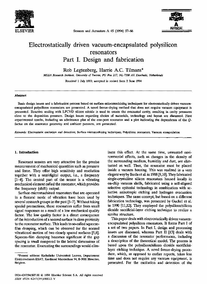
The basic structure of the resonator is shown in Fig. 1. The resonator consists of a prismatic beam with a rectangular cross section and is housed in an evacuated cavity. From an electric viewpoint, the structure defines a four-terminal device. Both the one- [6,14] and two- port approaches [5,7,10] can be used for excitation and detection. Details of the electric driving scheme are presented in the accompanying paper [13].
Electrostatic excitation and detection has been em- ployed [3-71. This is attractive because of its simplicity and compatibility with micromachining and IC tech- nologies. The simple structure makes the mechanical properties, and in particular the residual stress, much easier to control. Also, the scheme does not suffer from disturbing frequency shifts due to thermally induced axial loads. Moreover, no additional transducer ma- terials are required as would be necessary for some other drive and detection schemes, such as piezoelectric transduction. Thus, the electrostatic scheme provides an excellent way to achieve an ‘all-silicon device’, which is attractive for minimizing differential thermal-expan- sion effects.
2.2. The resonator
The static and dynamic characteristics of the resonator are determined by its in-plane geometry and by its characteristic dimensions perpendicular to the plane [4,13]. Flexural beam resonators were designed with lengths of 210, 310,410 and 510 hrn and widths of 25, 50 and 100 pm. The beam thickness is approximately 1.5 pm. Furthermore, a beam-to-substrate gap of ap- proximately 1.2 m and a beam-to-cap gap of 1.5 pm were chosen. These dimensions lead to theoreticalvalues of the static capacitance (excluding any parasitics) in
Evacuated cavity
I4 Substrate Fig. 1. Schematic cross section of a vacuum-encapsulated flexural beam resonator, depicted as a four-terminal device.
the range 0.03-0.3 pF. Parasitic loads, which are mainly capacitive, have to be kept very low or have to be compensated for in order to be able to detect the resonance [14]. The on-chip parasitic loads are mainly determined by the area of the bonding pads and the interconnecting wires. Thus, wire lengths were kept as short as possible and a relatively small bonding-pad area of 150 pm x 150 pm was used. This resulted in measured parallel capacitances in the range 0.5-14 pF (for the 210 ,um long beams), depending on the mea- surement configuration [13].
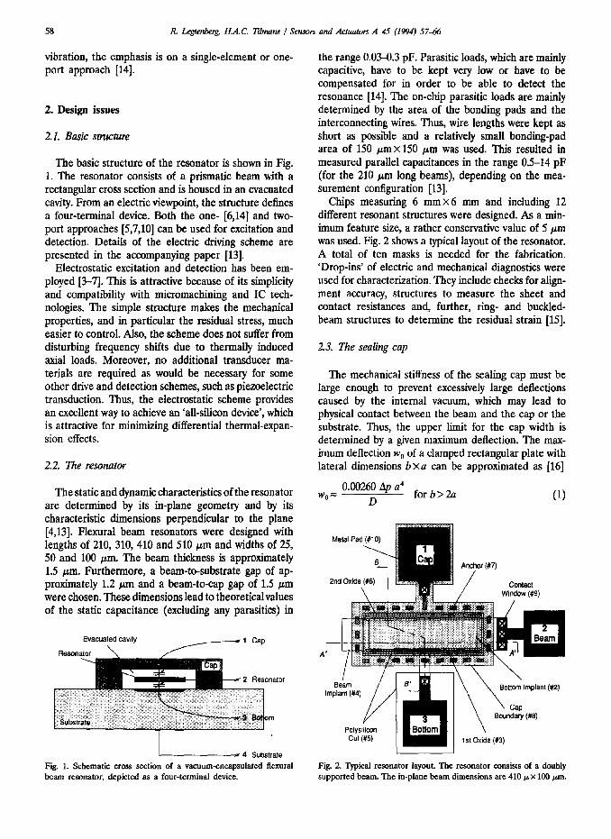
Chips measuring 6 mmx6 mm and including 12 different resonant structures were designed. As a min- imum feature size, a rather conservative value of 5 pm was used. Fig. 2 shows a typical layout of the resonator. A total of ten masks is needed for the fabrication. ‘Drop-ins’ of electric and mechanical diagnostics were used for characterization. They include checks for align- ment accuracy, structures to measure the sheet and contact resistances and, further, ring- and buckled- beam structures to determine the residual strain [U].
2.3. The sealing cap
The mechanical stiffness of the sealing cap must be large enough to prevent excessively large deflections caused by the internal vacuum, which may lead to physical contact between the beam and the cap or the substrate. Thus, the upper limit for the cap width is determined by a given maximum deflection. The max- imum deflection w0 of a clamped rectangular plate with lateral dimensions bxa can be approximated as [16]
We= om260 & a4 D
for b, 2a
Y Poly5iliwn cut (#5)
Fig. 2. mica1 resonator layout. The resonator consists of a doubly supported beam. The in-plane beam dimensions are 410 px 100 pm.
R. Leg&berg H.A.C. l&am I Sennrrs and Actuators A 45 (1994) 57-46 59
where Ap is the difference in pressure of the cavity interior and the ambient and D is the flexural rigidity of the plate. The coefficient 0.00260 depends on the length over width ratio b/a and is within two per cent accuracy if this ratio is larger than two. For a cap thickness of 2.5 pm, this leads to an upper limit of the width of approximately 150 pm if the maximum cap deflection should not exceed 0.5 pm. Finite-element analyses of a more realistic cap structure have indicated an increase of the maximum deflection of 20-30% due to small corrugations that are a result of the fabrication process (e.g., see Fig. 5(h)). This leads to a smaller value for the upper limit of the width. The cap thickness used is approximately 2.6 m, which is sufficient to keep the inward deflection after sealing below 0.5 q for 100 q wide beams.
3. Technology and materials
3.1. Surface micromachining
Surface micromachining is used to fabricate the po- lysilicon resonant structures. The technology relies on the construction of mechanical parts from a thin-film material in combination with a sacrificial-layer thin lilm that is used as a spacer between the structural parts [5,17,18]. After selective chemical removal of the sac- rificial layer, freely movable members remain. Surface micromachining offers small dimensions and a good dimensional control, especially in the thickness direc- tion. Further, a very elegant way to fabricate evacuated cavities by means of surface-micromachining techniques has recently been presented [17,19].
3.2. Materials
Taking planar silicon thin-film technology as a starting point, the aim is to develop an ‘all-silicon device’. This provides a good thermal match with the silicon substrate and, further, allows IC-compatible processing. Fabri- cation is based on the polysilicon/silicon dioxide sac- rificial-layer technique.
To obtain a high sensitivity of the frequency per unit applied strain, i.e., the gauge factor, slender beams are required with a low residual strain [4]. A tensile strain is desired to minimize the possibility of buckling. A tensile strain in the range 10-100 ppm is considered to be optimal. The residual stress of polysilicon can be well controlled provided that proper deposition conditions and annealing cycles are used [15,19-211. Polysilicon with a low tensile strain can be obtained by low-pressure chemical vapour deposition (LPCVD) from silane (SiH,) at processing temperatures close to the temperature of transition from amorphous to (poly)cxystalline layers (-580 “C [21]). Thermal an-
nealing in nitrogen converts the as-deposited built-in compressive strain into a controllable tensile strain depending on the annealing temperature [15].
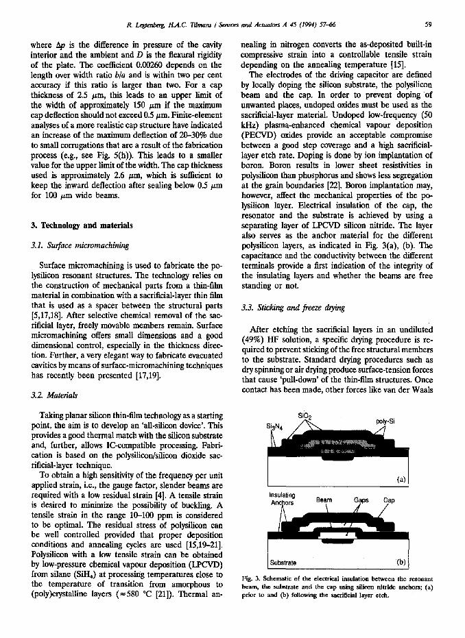
The electrodes of the driving capacitor are defined by locally doping the silicon substrate, the polysilicon beam and the cap. In order to prevent doping of unwanted places, undoped oxides must be used as the sacrificial-layer material. Undoped low-frequency (50 kHz) plasma-enhanced chemical vapour deposition (PECVD) oxides provide an acceptable compromise between a good step coverage and a high sacrificial- layer etch rate. Doping is done by ion implantation of boron. Boron results in lower sheet resistivities in polysilicon than phosphorus and shows less segregation at the grain boundaries [22]. Boron implantation may, however, affect the mechanical properties of the po- lysilicon layer. Electrical insulation of the cap, the resonator and the substrate is achieved by using a separating layer of LPCVD silicon nitride. The layer also serves as the anchor material for the different polysilicon layers, as indicated in Fig. 3(a), (b). The capacitance and the conductivity between the different terminals provide a first indication of the integrity of the insulating layers and whether the beams are free standing or not.
3.3. Sticking and freeze a?ying
After etching the sacrificial layers in an undiluted (49%) HF solution, a specific drying procedure is re- quired to prevent sticking of the free structural members to the substrate. Standard drying procedures such as dry spinning or air drying produce surface-tension forces that cause ‘pull-down’ of the thin-film structures. Once contact has been made, other forces like van der Waals
Insulating d
Substrate 0)
Fii 3. Schematic of the electrical insulation between the resonant beam, the substrate and the cap using silicon nitride anchors; (a) prior to and (b) following the sacrificial layer etch.
60 R. Legtentwtg H.A.C. Tihans / Sensors and Acttutors A 45 (I9!34) 57-66
forces, electrostatic forces, hydrogen bridging and chem- ical reactions come into play, resulting in permanent attachment of the structures to the substrate [23-251. An elegant way to solve this so-called sticking problem is ‘freeze drying’. The freeze-drying method was de- veloped as a drying method for biological specimens by Boyde and Wood in 1969 [26]. Guckel et al. [24] and later Takeshima et al. [27] implemented this tech- nique for sacrificial-layer etching of surface-microma- chined structures. They describe a process whereby a final rinsing agent is frozen and subsequently sublimated in a few hours under vacuum conditions.
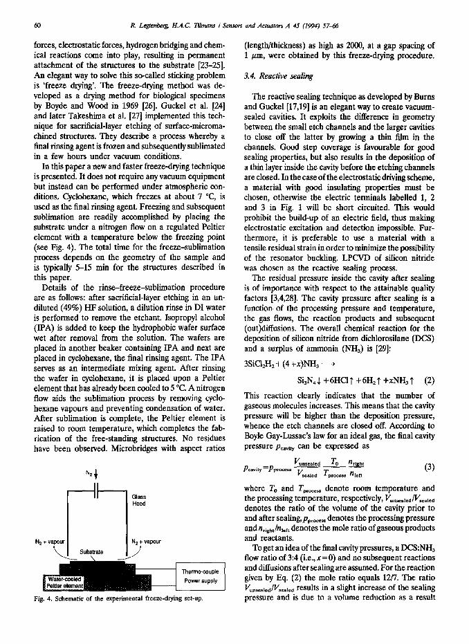
In this paper a new and faster freeze-drying technique is presented. It does not require any vacuum equipment but instead can be performed under atmospheric con- ditions. Cyclohexane, which freezes at about 7 “C, is used as the final rinsing agent. Freezing and subsequent sublimation are readily accomplished by placing the substrate under a nitrogen flow on a regulated Peltier element with a temperature below the freezing point (see Fig. 4). The total time for the freeze-sublimation process depends on the geometry of the sample and is typically 5-15 mm for the structures described in this paper.
Details of the rinse-freeze-sublimation procedure are as follows: after sacrificial-layer etching in an un- diluted (49%) HF solution, a dilution rinse in DI water is performed to remove the etchant. Isopropyl alcohol (IPA) is added to keep the hydrophobic wafer surface wet after removal from the solution. The wafers are placed in another beaker containing IPA and next are placed in cyclohexane, the final rinsing agent. The IPA serves as an intermediate mixing agent. After rinsing the wafer in cyclohexane, it is placed upon a Peltier element that has already been cooled to 5 “C. A nitrogen flow aids the sublimation process by removing cyclo- hexane vapours and preventing condensation of water. After sublimation is complete, the Peltier element is raised to room temperature, which completes the fab- rication of the free-standing structures. NO residues have been observed. Microbridges with aspect ratios
GhSS Hood
Fig. 4. Schematic of the experimental freeze-drying set-up.
(length/thickness) as high as 2000, at a gap spacing of 1 pm, were obtained by this freeze-drying procedure.
3.4. Reactive sealing
The reactive sealing technique as developed by Burns and Guckel[17,19] is an elegant way to create vacuum- sealed cavities. It exploits the difference in geometry between the small etch channels and the larger cavities to close off the latter by growing a thin film in the channels. Good step coverage is favourable for good sealing properties, but also results in the deposition of a thin layer inside the cavity before the etching channels are closed. In the case of the electrostatic driving scheme, a material with good insulating properties must be chosen, othexwise the electric terminals labelled 1, 2 and 3 in Fig. 1 will be short circuited. This would prohibit the build-up of an electric field, thus making electrostatic excitation and detection impossible. Fur- thermore, it is preferable to use a material with a tensile residual strain in order to minimize the possibility of the resonator buckling. LPCVD of silicon nitride was chosen as the reactive sealing process.
The residual pressure inside the cavity after sealing is of importance with respect to the attainable quality factors [3,4,28]. The cavity pressure after sealing is a function. of the processing pressure and temperature, the gas flows, the reaction products and subsequent (out)diffusions. The overall chemical reaction for the deposition of silicon nitride from dichlorosilane (DCS) and a surplus of ammonia (NH,) is [29]:
SSiCl,H, + (4 +x)NH, -
S&N, J + 6HCl t + 6H, 7 +xNH, t (2)
This reaction clearly indicates that the number of gaseous molecules increases. This means that the cavity pressure will be higher than the deposition pressure, whence the etch channels are closed off. According to Boyle Gay-Lussac’s law for an ideal gas, the final cavity pressure pcavity can be expressed as
(3) “Sealed 1 process %fl
where To and T,,,, denote room temperature and the processing temperature, respectively, Vu,_&d/V_l_, denotes the ratio of the volume of the cavity prior to and after sealing,p,,,, denotes the processing pressure and n,i,,,,/n,.ft denotes the mole ratio of gaseous products and reactants.
To get an idea of the final cavity pressures, a DCS:NH, flow ratio of 3:4 (i.e., x = 0) and no subsequent reactions and diffusions after sealing are assumed. For the reaction given by Eq. (2) the mole ratio equals 12/i’. The ratio V unsecaled/~caled results in a slight increase of the sealing pressure and is due to a volume reduction as a result
R Legtenbetg, HAC, lSnam / Sensors and Actuators A 45 (1994) 5766 61
of the inward deflection of the sealing cap. This de- flection is generally undesirable and is therefore kept small, resulting in a volume ratio close to unity. For a processing pressure of 200 mTorr (0.26 mbar) and a deposition temperature of 800 “C, Eq. (3) predicts a sealing pressure of about 100 mTorr (0.13 mbar). A more dedicated process performed at a pressure of 20 mTorr, a temperature of 850 “C and the same gas-flow ratio as indicated above leads to a sealing pressure of approximately 10 mTorr, but exhibits a lower deposition rate. By using a flow ratio DCS:NH, = 1:3, a surplus of ammonia results (i.e., x=5) and the mole ratio is equal to 17/12. This leads to a lowering of the final cavity pressure from 100 to 83 mTorr. Extending the surplus to infinity results in a final cavity pressure of 58 mTorr. These simple examples indicate that the mole ratio is not the determining factor, but, instead, the processing pressure and the processing temperature are the most important parameters in determining the final cavity pressure. Low final cavity pressures using a LPCVD silicon nitride sealing layer are obtained at a high deposition temperature and a low deposition pressure.
4. Fabrication sequence
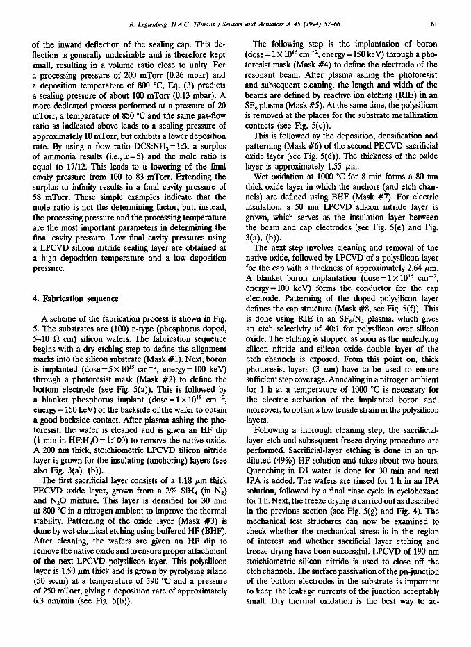
A scheme of the fabrication process is shown in Fig. 5. The substrates are (100) n-type (phosphorus doped, 5-10 fl cm) silicon wafers. The fabrication sequence begins with a dry etching step to define the alignment marks into the silicon substrate (Mask #l). Next, boron is implanted (dose=5 x 1015 cm-Z, energy= 100 keVj’ through a photoresist mask (Mask #2) to define the bottom electrode (see Fig. 5(a)). This is followed by a blanket phosphorus implant (dose = IX 10” cm-‘, energy= 150 keV) of the backside of the wafer to obtain a good backside contact. After plasma ashing the pho- toresist, the wafer is cleaned and is given an I-IF dip (1 min in HF:H20 = 1:lOO) to remove the native oxide. A 200 mu thick, stoichiometric LPCVD silicon nitride layer is grown for the insulating (anchoring) layers (see also Fig. 3(a), (b)).
The first sacrificial layer consists of a 1.18 pm thick PECVD oxide layer, grown from a 2% SiH, (in N,) and NzO mixture. This layer is densified for 30 min at 800 “C in a nitrogen ambient to improve the thermal stability. Patterning of the oxide layer (Mask #3) is done by wet chemical etching using buffered HF (BHF). After cleaning, the wafers are given an HF dip to remove the native oxide and to ensure proper attachment of the next LPCVD polysilicon layer. This polysilicon layer is 1.50 pm thick and is grown by pyrolysing silane (50 seem) at a temperature of 590 “C and a pressure of 250 mTorr, giving a deposition rate of approximately 6.3 nm/min (see Fig. 5(b)).
The following step is the implantation of boron (dose = 1 X 1Ol6 cm-‘, energy= 150 keV) through a pho- toresist mask (Mask #4) to define the electrode of the resonant beam. After plasma ashing the photoresist and subsequent cleaning, the length and width of the beams are defined by reactive ion etching (RIE) in an SF, plasma (Mask #5). At the same time, the polysilicon is removed at the places for the substrate metallixation contacts (see Fig. 5(c)).
This is followed by the deposition, densification and patterning (Mask #6) of the second PECVD sacrificial oxide layer (see Fig. 5(d)). The thickness of the oxide layer is approximately 1.55 pm.
Wet oxidation at 1000 “C for 8 min forms a 80 nm thick oxide layer in which the anchors (and etch chan- nels) are defined using BHF (Mask #7). For electric insulation, a 50 nm LPCVD silicon nitride layer is grown, which serves as the insulation layer between the beam and cap electrodes (see Fig. 5(e) and Fig. 3(a), (b)).
The next step involves cleaning and removal of the native oxide, followed by LPCVD of a polysilicon layer for the cap with a thickness of approximately 2.64 pm. A blanket boron implantation (dose= 1 x lOI cmw2, energy=100 keV) forms the conductor for the cap electrode. Patterning of the doped polysilicon layer defines the cap structure (Mask #8, see Fig. 5(f)). This is done using RIE in an SF,& plasma, which gives an etch selectivity of 40~1 for polysilicon over silicon oxide. The etching is stopped as soon as the underlying silicon nitride and silicon oxide double layer of the etch channels is exposed. From this point on, thick photoresist layers (3 pm) have to be used to ensure sufficient step coverage. Annealing in a nitrogen ambient for 1 h at a temperature of 1000 “C is necessary for the electric activation of the implanted boron and, moreover, to obtain a low tensile strain in the polysilicon layers.
Following a thorough cleaning step, the sacrificial- layer etch and subsequent freeze-drying procedure are performed. Sacrificial-layer etching is done in an un- diluted (49%) HF solution and takes about two hours. Quenching in DI water is done for 30 mln and next IPA is added. The wafers are rinsed for 1 h in an IPA solution, followed by a final rinse cycle in cyclohexane for 1 h. Next, the freeze drying is carried out as described in the previous section (see Fig. 5(g) and Fig. 4). The mechanical test structures can now be examined to check whether the mechanical stress is in the region of interest and whether sacrificial layer etching and freeze drying have been successful. LPCVD of 190 mu stoichiometric silicon nitride is used to close off the etch channels. The surface passivation of the pn-junction of the bottom electrodes in the substrate is important to keep the leakage currents of the junction acceptably small. Dry thermal oxidation is the best way to ac-
62 R. Legtenberg, H.A.C. Ti1man.s I Sensors and Actuators A 45 (1994) 57-66
. PECVD (1st) SiOz -etch SiO, - LPCVD polySi
Baron lmdnmanan .
I - I Boron ImDlantation
(c) 1 - RIE polyki
. PECVD (2nd) Si02 etch SIO 2
wet oxidetiin . etch SiO, - LPCVD Si,N,
LPCVD polySi - Boron Implantation RIE polySi
. Saw. layer etching Freeze dQing
- LPCVD Si,N,
RIE Si3N, - PVD Al
doped Poly-Si
SisN4 insulating Bottom layers Electrode
Silicon Substrate (0
Fig. 5. Processing sequence for sealed polysilicon resonators. The different stages of the process are explained in the text: (a)-(h) cross- sectional view B-B’; (i) cross-sectional view A-A’ of Fig. 2.
complish this, but experiments revealed buckled beams even after growing oxide layers as thin as 10 nm at a temperature of 800 “C. It was found that the leakage currents of the pn-junctions that are passivated with silicon nitride are of the order of 10 PA cm-*, which is considered to be satisfactory.
The contact windows for the substrate, beam and cap electrodes are defined using RIE in a CHFJO, plasma (Mask #9). Metallization consists of a 1 pm thick aluminium layer. Prior to the metallization, the thin films that have accumulated on the backside of the wafer are stripped by means of RIE in SF, and CHF, plasmas. Metal patterning (Mask #lo) is done by wet chemical etching. The final step is a 5 min anneal in an N&&O ambient at 450 “C to obtain good ohmic contacts. Final cross sections of the sealed res- onator are shown in Fig. 5(h) and (i).
5. First results
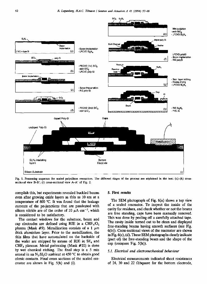
The SEM photograph of Fig. 6(a) shows a top view of a sealed resonator. To inspect the inside of the cavity for residues, and check whether or not the beams are free standing, caps have been manually removed. This was done by peeling off a carefully attached tape. The cavity inside turned out to be clean and displayed free-standing beams having smooth surfaces (see Fig. 6(b)). Cross-sectional views of the resonator are shown in Fig. 6(c), (d). These SEM photographs clearly indicate (part of) the free-standing beam and the shape of the cap (compare Fig. 5(h)).
5.1. Electrical and electromechanical behaviour
Electrical measurements indicated sheet resistances of 24, 30 and 22 a/square for the bottom electrode,
R Legtenbetg HAC. Tilmam I Semm and Actuators A 45 (1994) 57-66 63
Fig. 6. SEM photographs of sealed polysilicon resonators: (a) top view of a resonator; lb) resonator with cap removed; (c) cross-sxctional view, (d) magnified view of part of the cross section.
the resonator electrode and the cap electrode, re- spectively. Tbe contact resistance turned out to be about 1 R for a 20 PmX 20 pm contact for all three electrodes. Standard 1-P’ measurements used to check the integrity of the nitride insulating anchors revealed high ohmic (Gfls) anchors. The residual strain has been extracted from the polysilicon ring and buckled- beam diagnostics and is within the range -8X lo-’ (compressive) to + 6 X 10e5 (tensile).
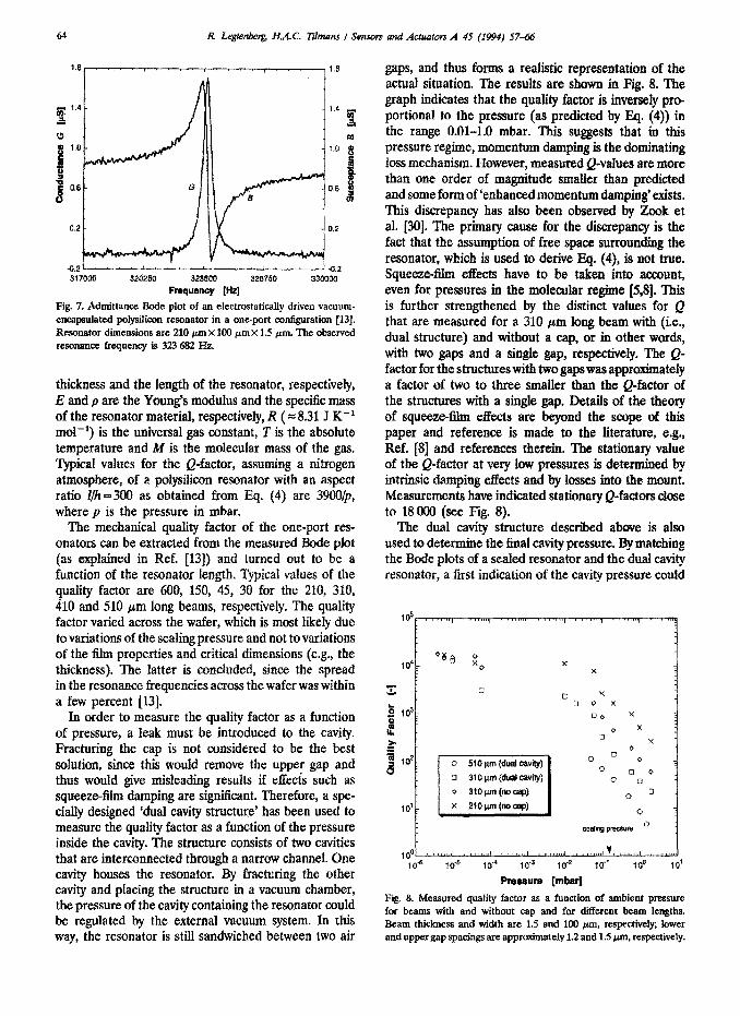
First tests aimed at finding the resonance frequency have indicated that care must be taken with respect to probing the samples. Static charges induce electric forces that cause ‘pull-in’ of the beams, resulting in permanent attachment of the latter to the cap or to the substrate. This phenomenon was observed while testing uncapped resonators. Fig. 7 shows a typical example of a measured Bode plot showing the con- ductance and the susceptance as functions of the driving frequency of a 210 brn long polysilicon beam resonator. Details of the measurement set-up are described in the accompanying paper [13].
5.2. Quality factor and sealing pressure
Vacuum sealing provides pressures in the molecular regime, where the gas molecules are not interacting with each other. Energy losses due to viscous damping are negligible in this pressure regime. The damping mechanisms that remain include losses due to individual collisions of the gas molecules with the resonating surfaces (momentum damping), losses into the mount and intrinsic (material) damping. If momentum damping is considered to be the dominant loss mechanism and if the resonator was operating in free space, the me- chanical quality factor as a function of the ambient pressure p can be expressed as [28]
(4)
where an is a dimensionless constant depending on the edge conditions and on the mode of vibration n (aI = 4.73 for a clamped-clamped beam [4]), h and 1 are the
64 R. Lxgtenberg H.4.C. lihans I Sensors and Actuators A 45 (lW4) 5766
_0.2’ / I I :-o,2
317oGa 320250 323500 326750 33Giw Frequency [Hz]
Fig. 7. Admittance Bode plot of an electmstaticalJy driven vacuum- encapsulated polysilicon resonator in a one-port ConEguration [13]. Resonator dimensions are 210 m x 100 pm X 1.5 PITI. The observed resonance frequency is 323 632 Hz
thickness and the length of the resonator, respectively, E and p are the Young’s modulus and the specific mass of the resonator material, respectively, R ( = 8.31 J K-’ mol-I) is the universal gas constant, 2’ is the absolute temperature and M is the molecular mass of the gas. ‘@pica1 values for the Q-factor, assu~ng a nitrogen atmosphere, of a polysilicon resonator with an aspect ratio l/h=300 as obtained from Eq. (4) are 3900/p, where p is the pressure in mbar.
The mechanical quality factor of the one-port res- onators can be extracted from the measured Bode plot (as explained in Ref. [13]) and turned out to be a function of the resonator length. Typical values of the quality factor are 600, 150, 45, 30 for the 210, 310, 410 and 510 km long beams, respectively. The quality factor varied across the wafer, which is most likely due to variations of the sealing pressure and not to variations of the t&n properties and critical dimensions (e.g., the thickness}. The latter is concluded, since the spread in the resonance frequencies across the wafer was within a few percent [13].
In order to measure the quality factor as a function of pressure, a leak must be introduced to the cavity. Fracturing the cap is not considered to be the best ~lution, since this would remove the upper gap and thus would give misleading results if effects such as squeeze-film damping are significant. Therefore, a spe- cially designed ‘dual cavity structure’ has been used to measure the quality factor as a function of the pressure inside the cavity. The structure consists of two cavities that are in~r~nnected through a narrow channel. One cavity houses the resonator. By fracturing the other cavity and placing the structure hr a vacuum chamber, the pressure of the cavity containing the resonator could be regulated by the external vacuum system. In this way, the resonator is still sandwiched between two air
gaps, and thus forms a realistic repr~ntation of the actual situation. The results are shown in Fig. 8. The graph indicates that the quality Eactor is inversely pro- portional to the pressure (as predicted by Eq. (4)) in the range 0.01-1.0 mbar. This suggests that in this pressure regime, momentum damping is the dominating loss mechanism. However, measured Q-values are more than one order of magnitude smaller than predicted and some form of ‘enhanced momentum damping’ exists. This discrepancy has also been observed by tik et al. [30]. The primary cause for the discrepancy is the fact that the assumption of free space surrounding the resonator, which is used to derive Eq (41, is not true. Squeeze-t&n effects have to be taken into account, even for pressures in the molecular regime [5,8]. This is further strengthened by the distinct values for Q that are measured for a 310 pm long beam with (i.e., dual structure) and without a cap, or in other words, with two gaps and a single gap, respectively. The Q- factor for the structures with two gaps was a~~ately a factor of two to three smaller than the Q-factor of the structures with a single gap. Details of the theory of squeeze-film effects are beyond the scope of this paper and reference is made to the literature, e.g., Ref. [S] and references therein. The stationary value of the Q-factor at very low pressures is dete~ed by intrinsic damping effects and by losses into the mount. Measurements have indicated stationary Q-factors close to 18 000 (see Fig. 8).
The dual cavity structure described above is also used to determine the final cavity pressure. By matching the Bode plots of a sealed resonator and the dual cavity resonator, a first ~ndi~tion of the cavity pressure could
‘“m x
x
Fig. 8. Measured quality factor as a function of ambient pressure for beams with and without cap and for dierent beam lengths. Beam thickness and width are 1.5 and 100 m, respectively; lower and upper gap spacings are approximately 1.2 and 1.5 w, respectively.
R. Legtenberg HAC. Tibnans I Sensors and Actuators A 45 (1994) 57-66 65
be obtained. This revealed sealing pressures in the range 0.142 mbar, which is in agreement with the predicted value (~0.13 mbar) from Eq. (3).
More experimental data together with a theoretical model of the resonator behaviour are given in the accompanying paper [ 131.
6. Conclusions
Resonators housed in evacuated cavities have been successfully fabricated with surface micromachining us- ing sacrificial-layer spacers. Low-strain fine-grained LPCVD polysilicon has been used for the structural parts and undoped PECVD silicon oxide as the sac- rificial-layer material. Electrostatic excitation and de- tection was used as the driving and sensing mechanism. Electrical insulation of the different electrodes is ac- complished by means of LPCVD silicon nitride layers. A novel freeze-drying method using cyclohexane has been developed to prevent sticking. The advantages of this procedure as compared to other known freeze- drying procedures are its enhanced speed and the fact that no vacuum equipment is required. Reactive sealing with LPCVD silicon nitride yields cavity pressures close to the processing pressure. First measurements have indicated the typical resonance characteristics that are expected for resonators operated in a one-port con- figuration. Quality factors are determined by enhanced momentum damping (for pressures in the molecular regime) due to squeeze-film effects, and turn out to be inversely proportional to the ambient pressure for moderate sealing pressures (0.01-1.0 mbar). Measured sealing pressures are estimated to be in the range 0.142 mbar, resulting in quality factors close to 600 for the 210 pm long beams. A more dedicated sealing procedure at lower deposition pressures and/or higher temperatures is required to obtain cavity pressures in the regime where the quality factor is independent of pressure and is solely determined by intrinsic losses and losses into the mount. Subsequent annealing at elevated temperatures may further reduce the sealing pressure due to outdifision of gaseous species. Mea- surements have indicated that quality factors close to 18 000 are feasible at pressures below 0.01 mbar.
Acknowledgements
The authors acknowledge Dr Miko Elwenspoek, Pro- fessor Dr Jan Fluitman and Professor Dr Theo Popma of the Micromechanics Group for their interest and support. Further, they thank the staff of the MESA Laboratory of the University of Twente, in particular Arie Kooy for mask fabrication, and Eddy de Ruiter, Tom Aarnink and Gerrit Boom for doing the ion
implantations. Also they would like to thank Dick Ekkelkamp for his technical support and Hans Schurer for doing the Q-factor measurements. This research is part of the programme of the Dutch Foundation for Fundamental Research on Matter (FOM) and is spon- sored by the Dutch Technology Foundation (SW).
References
M
VI
131
I41
151
PI
[71
PI
[91
WI
WI
I131
1141
P51
WI
RM. Langdon, Resonator sensors - a review, 1. Phys E: Sci Insbum., 18 (1985) 103-115. R.T. Howe, Resonant microsensors, Pmt. 4th hat. Conf Solid- State Sensors tmd Actuators (Tmnwizcetx ‘87), Tokyo, Japan, June 2-5, 1987, pp. 843-848. G. Stemme, Resonant silicon sensors, 3. hficromech. Microeng, Z (1991) 113-125. H.A.C. Tihnans, M. Elwenspock and J.H.J. Fluitman, Micro resonant force gauges, Sensors andActuatorsA, 30 (1992) 35-53. R.T. Howe and R.S. Muiler, Resonant-microbridgevapor sensor, IEEE Tmns. Elechon Devices, ED-33 (1986) 499-506. M.W. Putty, S.C. Chang, R.T. Howe, A.L. Robinson and K.D. Wise, One-port active polysilicon resonant microstmctures&x IEEE Micro Ekchv Mechanical Sy@ms, Salt Lake City, UT. USA, Feb. 20-22, 1989, pp. 60-65. C tinder, I?. Zimmerman and N.F. de Rooij, Capacitive polysilicon resonator with MOS detection circuit, Sensors and Achutors A, 25-27 (1991) 591495. M. Andrews, I. Harris and G. Turner, A comparison of squeeze- film theory with measurements on a microstructure, Sensors and Actuators A, 36 (1993) 79-87. K. Ikeda, H. Kuwayama, T. Kobayashi, T. Watanabe, T. Ni- shiiawa and T. Yoshida, Three dimensional micromachining of silicon resonant strain gauge, Pmt. 7th Sensor Syrnp., Tokyo, Japan, 1988, pp. 193-196. K. Ikeda, H. Kuwayama, T. Kobayashi, T. Watanabe, T. Ni- shikawa and T. Ycshida, Silicon pressure sensor with resonant strain gauge built into diaphragm, Pmt. 7th Sensor Syrup., Tokyo, Japan, 19.38, pp. 55-58. H. Guckel, J.J. Sniegowski, T.R. Christenson and F. Raissi, The application of fme-grained, tensile polyailicon to mechan- ically resonant transducers, Sen.wts and Actuators, A21423 (1990) 346-351. J.J. Sniegowski, H. Guckel and T.R. Christenson, Performance characteristics of second generation polysilicon resonating beam force transducers, &oc. IEEE Solid-State Sensors and A&a&m W&hop, Hilton Head IsIand, SC, USA, June 4-7, Z9w. pp. %12. H.A.C. Tihnans and R. Legtenberg, Electrostatically driven vacuum-encapsulated polysiticon resonators; Part II - Theory and performance, Sensors and Actuators A, 44 (1994). H.A.C. Tihnans, D.J. Llntema and J.H.J. Fluitman, Single element excitation and detection of (micro-) mechanical res- onators, Pmt. 6th I&. Cons:, Solid-Stale Sensom and Actuators (Tmnsducers ‘9Z), San Francisco, USA, June 24-28, 1991, pp. 53s537. H. Guckel, D.W. Burns, H.A.C. Tilmans, D.W. DeRm and CR. Rutigliano, Mechanical properties of fine grained poly- silicon: the repeatability issue, IEEE Solid-State Sensors Work- shop, H&n Head Iskwtd, SC, USA, June 6-9, 1988, pp. 96-99. S.P. Timoshenko and S. Woinowsky-Krieger, Theory of P&s and She.%, McGraw-Hill, New York, 2nd edn., 1970, p. 202.
R. Legtenbe~ HA-C. li1man.v I Sensors and Actuators A 45 (1994) 57-66 66
P71
P81
1191
PO1
PI
1261
m
PI
v91
[301
H. Guckel and D.W. Burns, A technology for integrated trans- ducers, Rot. 3rd bt. Cottf Solid State Sensors and Actuators (Tmttsducers ‘85), Philade@hia, PA, USA, June U-14, 1985, pp. 90-92. RT. Howe, Surface micromaching for microsensors and mi- croactuators, J. Vat. Sci. Tech& B, 6 (6) (1988) 1809-1813. D.W. Bums, Micromechanics of integrated sensors and the planar processed pressure transducers, Ph.D. 7?testk, Dept. of Materials Science, University of Wisconsin, Madison, WI, USA, 1968. RT. Howe and R.S. ML&I, Stress in polycrystalline and amorphous silicon thin films, I. A&. Phys., 54 (8) (1983) 4674-4675. T.I. Kamins, Design properties of polycrystalline silicon, Sen.uxs and Actuators, A21-A23 (1990) 817-824. J.C. North, A.C. Adam and G.F. Richards, Ion implantation doping of polycrystalline silicon, Electmchem Sot. Fall Meet., Pi&u& PA, USA, &tended Ahw. 78-2, 1978, p. 542. P. Scheeper, J.A. Voorthuyzen and P. Bergveld, Surface forces in micromachined structures, Tech. Digest, MME ‘90,&f work- shop Micmmoch%ig Micromechanics Microsyslemr, Berlin, Ger- meny, Nov. 26-27, 1990, pi, 47-52. H. Guckel, J.J. Sniegowski, T.R. Christenson, S. Mohney and T.F. Kelly, Fabrication of micromechanical devices from po- lysilicon films with smooth surfaces, Sensors and Achrotors, 20 (1989) 117-122. R. Legtenberg, H.A.C. Tibnans. J. Elders and M. Elwenspcek, Stiction of surface micromachined structures after rinsing and drying: model and investigation of adhesion mechanisms, Senrors and Actuators A, 43 (1994) 230-238. A. Boyde and C. Wood, Preparation of animal tissues for surface-scanning electron microscopy, 1 Microsc., 90 (1969) 221-249. N. Takeshima, K.J. Gabriel, M. Ozaki, J. Takahasji, H. Horiguchi and H. Fujita, Electrostatic parallelogram actuators, Pmt. 6th htt. Confi Solid-State Senrors and Acttutors (Tmtwducers 91), San Fmncisco, CA, USA, June 24-28, 1991, pp. 63-66. F.R. Blom, S. Bouwstra, M. Elwenspoek and J.&J. Fluitman, Dependence of the quality factor of micromachined silicon beam resonators on pressure and geometry, 1. Voc. Sci. Technol. E, 10 (1992) 19-26. K.F. Roenigk and K.F. Jensen, Low pressure CVD of silicon nitride, 1. Electmchem Sot., 134 (1987) 1777-1885. J.D. &ok, D.W. Burns, H. Guckel, J.J. Sniegowski, R.L. Engelstad and Z. Feng, Characteristics of polysilicon resonant microbeams, Sensors and Acttutors A, 35 (1992) 51-59.
Biographies
Rob Legtenberg was born on June 21,1964, in Hengelo, The Netherlands. He received the B.Sc. degree in
applied physics from the Hogere Technische School Enschede, Enschede, The Netherlands, in June 1985. After fulfilling his military service, he joined the MicroMechanical Research Group at the University of Twente as a process engineer in September 1986. Since April 1992 he has been preparing for his Ph.D., dealing with the development of actuators based on surface- micromachining technology.
Ham.e Tilmans was born on November 14, 1957, in Elsloo, The Netherlands. He received his M.Sc. degree in electrical engineering from the University of Twente, Enschede, The Netherlands, in May 1984. In June 1984 he became a temporary researcher at the University of Twente, where he worked on the development of a resonating force sensor. In April 1985 he joined the Faculty of Electrical and Computer Engineering of Boston University, Boston, MA, USA, as a visiting instructor. In August 1986 he became a research assistant at the Wisconsin Center for Applied Microelectronics at the University of Wisconsin, Madison, WI, USA, where he worked on the development of a CMOS process and on the development of polysilicon micro- mechanical resonators. In August 1988 he returned to The Netherlands, where he joined the MESA Research Institute of the University of Twente as a research associate to work on ‘micromechanical sensors using encapsulated built-in resonant strain gauges’. He re- ceived his Ph.D. degree on this topic in January 1993. From August 1989 till January 1990 he wa’s on leave from the university at the Sensors Group of the Controls Research Department of Johnson Controls Inc., Mil- waukee, WI, USA, working on a low-range differential pressure sensor. From September 1, 1992 till August 1, 1993 he was employed by FOM (Foundation for Fundamental Research on Matter, The Netherlands) in a postdoctorate position within the Micromechanics Group of the MESA Research Institute to work on the characterization of mechanical properties of thin films. He is currently employed by the Catholic Uni- versity of Leuven in Belgium to continue his work on microsystems technology.