30
ELEN 701 RF & Microwave Systems Engineering Lecture 8 November 8, 2006 Dr. Michael Thorburn Santa Clara University
ELEN 701 RF & Microwave Systems Engineering
Lecture 8November 8, 2006
Dr. Michael ThorburnSanta Clara University
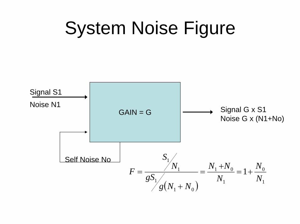
System Noise Figure
GAIN = G
Signal S1
Noise N1
Self Noise No
Signal G x S1Noise G x (N1+No)
( ) 1
0
1
01
01
1
1
1
1NN
NNN
NNggS
NS
F +=+
=
+
=
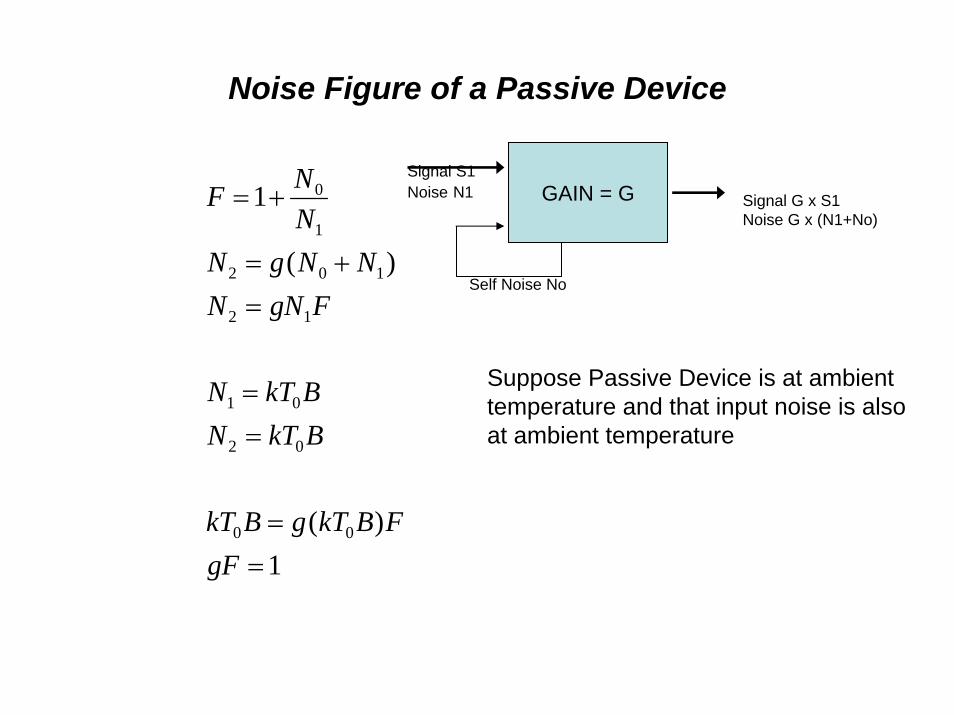
Noise Figure of a Passive Device
1)(
)(
1
00
02
01
12
102
1
0
==
==
=+=
+=
gFFBkTgBkT
BkTNBkTN
FgNNNNgN
NNF
Suppose Passive Device is at ambienttemperature and that input noise is also at ambient temperature
GAIN = GSignal S1Noise N1
Self Noise No
Signal G x S1Noise G x (N1+No)
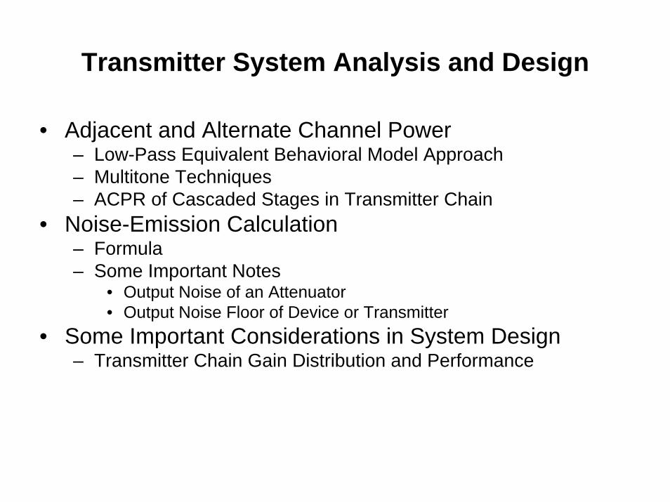
Transmitter System Analysis and Design
• Adjacent and Alternate Channel Power– Low-Pass Equivalent Behavioral Model Approach– Multitone Techniques– ACPR of Cascaded Stages in Transmitter Chain
• Noise-Emission Calculation– Formula– Some Important Notes
• Output Noise of an Attenuator• Output Noise Floor of Device or Transmitter
• Some Important Considerations in System Design– Transmitter Chain Gain Distribution and Performance
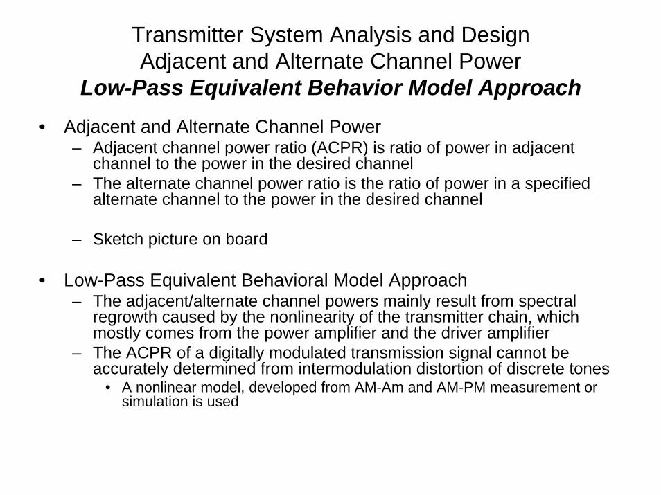
Transmitter System Analysis and DesignAdjacent and Alternate Channel Power
Low-Pass Equivalent Behavior Model Approach• Adjacent and Alternate Channel Power
– Adjacent channel power ratio (ACPR) is ratio of power in adjacent channel to the power in the desired channel
– The alternate channel power ratio is the ratio of power in a specified alternate channel to the power in the desired channel
– Sketch picture on board
• Low-Pass Equivalent Behavioral Model Approach– The adjacent/alternate channel powers mainly result from spectral
regrowth caused by the nonlinearity of the transmitter chain, which mostly comes from the power amplifier and the driver amplifier
– The ACPR of a digitally modulated transmission signal cannot be accurately determined from intermodulation distortion of discrete tones
• A nonlinear model, developed from AM-Am and AM-PM measurement or simulation is used
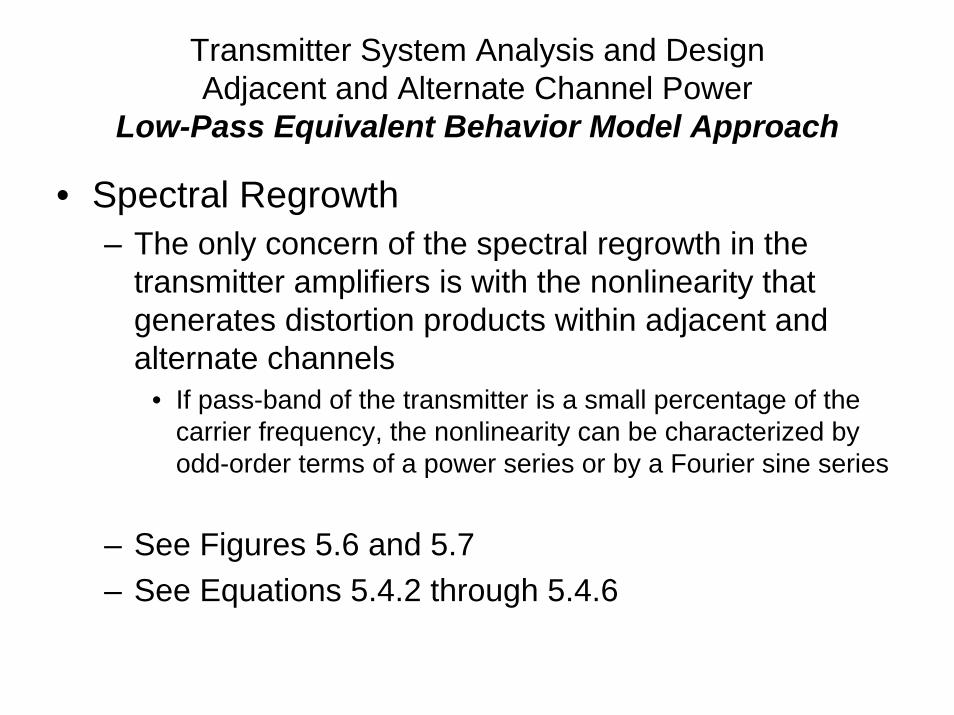
Transmitter System Analysis and DesignAdjacent and Alternate Channel Power
Low-Pass Equivalent Behavior Model Approach
• Spectral Regrowth– The only concern of the spectral regrowth in the
transmitter amplifiers is with the nonlinearity that generates distortion products within adjacent and alternate channels
• If pass-band of the transmitter is a small percentage of the carrier frequency, the nonlinearity can be characterized by odd-order terms of a power series or by a Fourier sine series
– See Figures 5.6 and 5.7– See Equations 5.4.2 through 5.4.6

Transmitter System Analysis and DesignAdjacent and Alternate Channel Power
Multitone Techniques
• Two-tone measurements are commonly used in determining the intermodulation distortion characteristics
• In digital mobile communications, signals are more complicated and their spectral regrowthcannot be accurately analyzed in terms of the two-tone IMD– It becomes necessary to apply the multitone signals
to analytically asses the ACPR of tranmission signals– The n-tone ACPR formula is found in equation 5.4.7
• This does not work for alternate channel power regrowth as it is mainly caused by fifth order nonlinear distortion of the PA
Transmitter System Analysis and DesignAdjacent and Alternate Channel Power
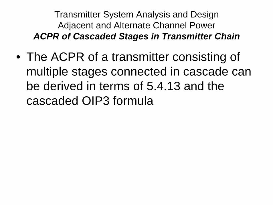
ACPR of Cascaded Stages in Transmitter Chain
• The ACPR of a transmitter consisting of multiple stages connected in cascade can be derived in terms of 5.4.13 and the cascaded OIP3 formula
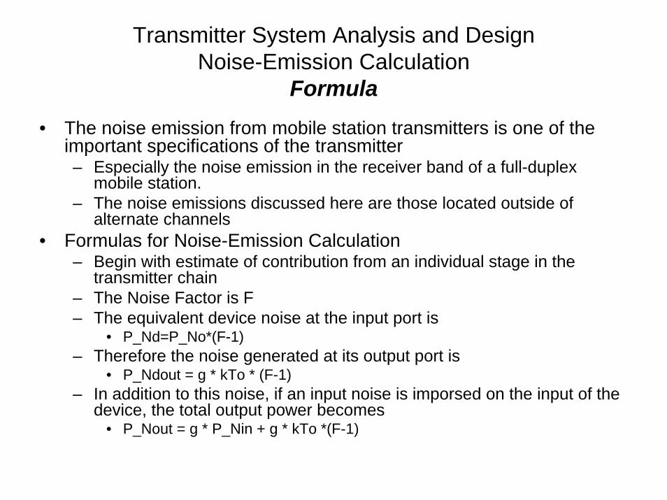
Transmitter System Analysis and DesignNoise-Emission Calculation
Formula• The noise emission from mobile station transmitters is one of the
important specifications of the transmitter– Especially the noise emission in the receiver band of a full-duplex
mobile station. – The noise emissions discussed here are those located outside of
alternate channels• Formulas for Noise-Emission Calculation
– Begin with estimate of contribution from an individual stage in the transmitter chain
– The Noise Factor is F– The equivalent device noise at the input port is
• P_Nd=P_No*(F-1)– Therefore the noise generated at its output port is
• P_Ndout = g * kTo * (F-1)– In addition to this noise, if an input noise is imporsed on the input of the
device, the total output power becomes• P_Nout = g * P_Nin + g * kTo *(F-1)

Transmitter System Analysis and DesignNoise-Emission Calculation
Formula
• For a transmitter consisting of n stages, the noise emission has a similar formula– P_Nout = g_tx * P_Nin + g_tx * kTo *(F_tx-1)– Where g_tx is overall transmitter gain– And where F_tx is the overall noise factor of the transmitter
Transmitter System Analysis and DesignNoise-Emission Calculation
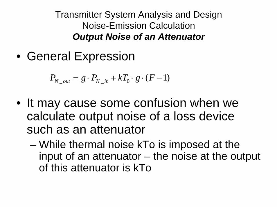
Output Noise of an Attenuator
• General Expression
• It may cause some confusion when we calculate output noise of a loss device such as an attenuator– While thermal noise kTo is imposed at the
input of an attenuator – the noise at the output of this attenuator is kTo
)1(0__ −⋅⋅+⋅= FgkTPgP inNoutN

Transmitter System Analysis and DesignNoise-Emission Calculation
Output Noise Floor of Device or Transmitter
• Minimum Input Noise of a Device is the thermal noise kTo
Transmitter System Analysis and DesignTransmitter Chain Gain Distribution and Performance
• See spreadsheets
Applications of System Design
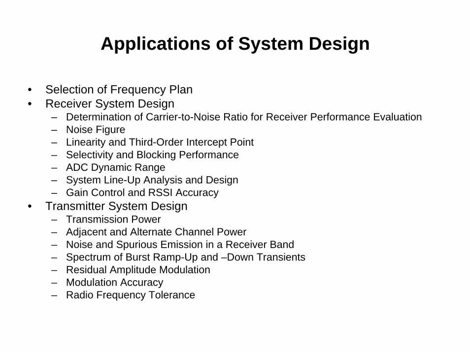
• Selection of Frequency Plan• Receiver System Design
– Determination of Carrier-to-Noise Ratio for Receiver Performance Evaluation– Noise Figure– Linearity and Third-Order Intercept Point– Selectivity and Blocking Performance– ADC Dynamic Range– System Line-Up Analysis and Design– Gain Control and RSSI Accuracy
• Transmitter System Design– Transmission Power– Adjacent and Alternate Channel Power– Noise and Spurious Emission in a Receiver Band– Spectrum of Burst Ramp-Up and –Down Transients– Residual Amplitude Modulation– Modulation Accuracy– Radio Frequency Tolerance

Applications of System DesignSelection of Frequency Plan
• For Superheterodyne architecture – this amounts to:– Understanding the Frequency Band Allocation
(Regulation)– Selection of the receive IF frequency
• Resulting determination of the transmit IF• Resulting determination of the LO
– Need to do a spur analysis• Understand mixer spurs• Understand harmonics of power amplifiers• Understand IMs of power amplifiers in multicarrier
applications– Need to define filter requirements for spurs

Applications of System DesignReceiver System Design
Determination of Carrier-to-Noise Ratio for Receiver Performance Evaluation and Noise Figure
• Determine required receiver sensitivity• Determine required receiver NF• Assemble line-up of elements within the receiver
and determine the cascaded NF and the corresponding various component gain and NFs– DESIGN is an iterative process
• Select Components from catalog of available parts• Develop components as required• Ensure sensitivity requirements are satisfied
• Keep in mind degradations in receiver sensitivity due to output power spectrum in receive band
Applications of System DesignReceiver System Design
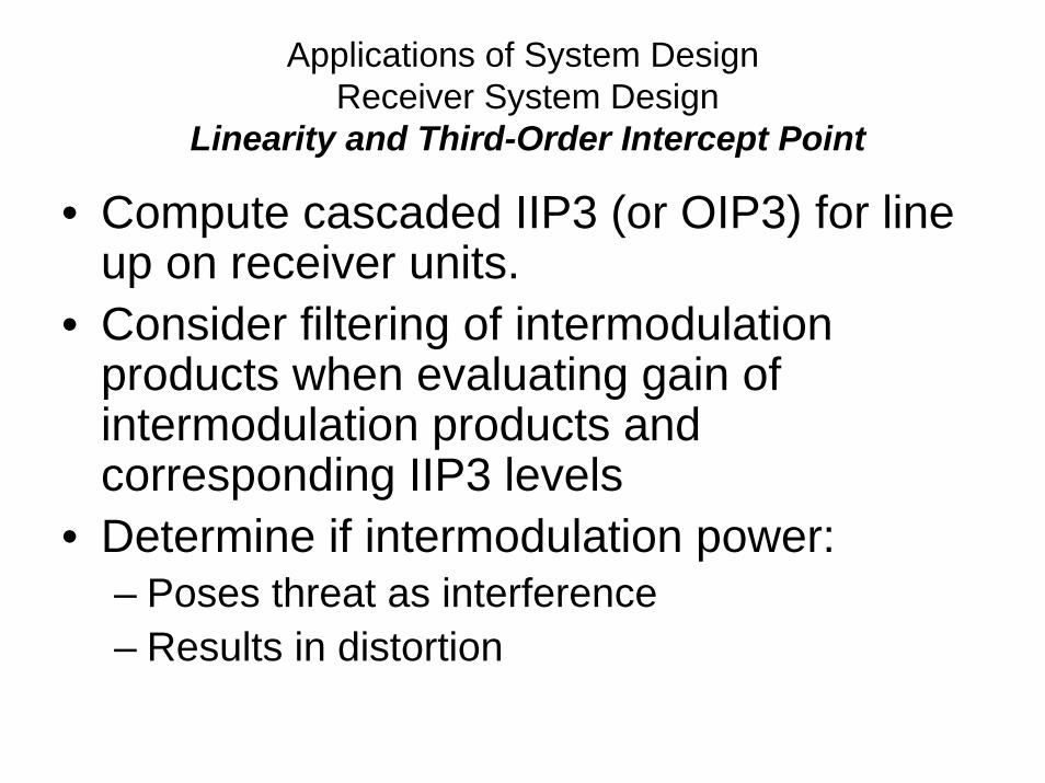
Linearity and Third-Order Intercept Point
• Compute cascaded IIP3 (or OIP3) for line up on receiver units.
• Consider filtering of intermodulationproducts when evaluating gain of intermodulation products and corresponding IIP3 levels
• Determine if intermodulation power:– Poses threat as interference– Results in distortion

Applications of System DesignReceiver System Design
Selectivity and Blocking Performance
• Selectivity– Design channel filters so that desired signal
passes “undistorted” and adjacent/alternate channels are rejected
• Parameters include:– Insertion Loss– Passband flatness– Passband gain slope– Passband group delay and group delay slope– Out of band rejection– Spuriuos rejection

Applications of System DesignReceiver System DesignADC Dynamic Range
• Develop line up of units in receiver• Determine input power range• Determine signal level through transceiver
– Target acceptable range of levels of input for ADC to work properly
– Determine to what degree ALC is required• ALC=automatic level control. e.g. VGA with
feedback control
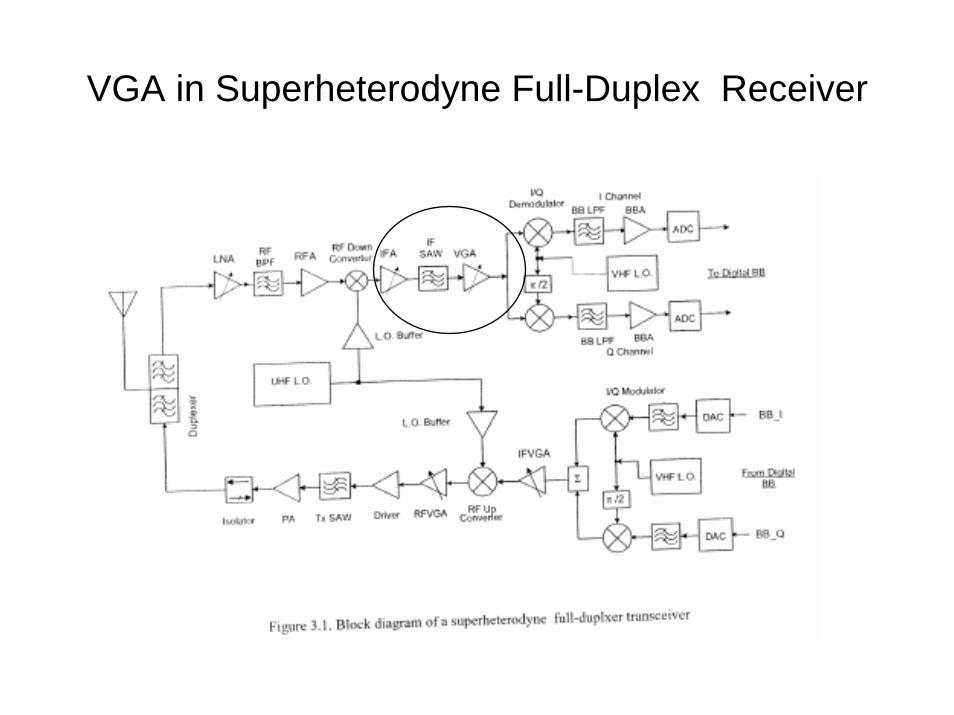
VGA in Superheterodyne Full-Duplex Receiver

Applications of System DesignReceiver System Design
System Line-Up Analysis and Design
• Clearly the system line-up is a key component of the system design– Allow for “drop in” of available units– Track:
• Signal strength• Noise Power• Cascaded Noise Figure• Cascaded IIP
– Note:• Spurious frequencies• LO power level• Channel selectivity (filter) requirements• Input signal power• Threshold BER
Applications of System DesignReceiver System Design
Gain Control and RSSI Accuracy• Selection of Frequency Plan• Receiver System Design
– Determination of Carrier-to-Noise Ratio for Receiver Performance Evaluation– Noise Figure– Linearity and Third-Order Intercept Point– Selectivity and Blocking Performance– ADC Dynamic Range– System Line-Up Analysis and Design– Gain Control and RSSI Accuracy
• Transmitter System Design– Transmission Power– Adjacent and Alternate Channel Power– Noise and Spurious Emission in a Receiver Band– Spectrum of Burst Ramp-Up and –Down Transients– Residual Amplitude Modulation– Modulation Accuracy– Radio Frequency Tolerance
Applications of System DesignTransmitter System Design
Transmission Power
• Transmission Power of Transceiver is combined with Antenna Gain to give EIRP– Key parameter in link– Establishes (largely) the DC power
requirements of transceiver– Establishes thermal design (if applicable)– Cost driver
• Cornerstone of transmitter design
Applications of System DesignTransmitter System Design
Adjacent and Alternate Channel Power
• Significant concern of transmitter is spectral regrowth and resulting undesired power in adjacent or alternate channels– Interference to other users of system– Drives linearity concerns in transmitter design
• Cascaded IIP is typical quantity tracked• AM/AM and AM/PM characteristics provide details as to
regrowth– Post amplifier filters may be used to limit out of band
power• At expense of insertion loss and wasted DC power• At expense of thermal design for high power transmitters

Applications of System DesignTransmitter System Design
Noise and Spurious Emission in a Receiver Band
• Significant signal level differences between receive and transmit signals– e.g. ~-100 dBm vs. 30 dBm
• Design must ensure adequate rejection of noise and spurious signals in receive band– Degrades receiver sensitivity– May damage RF front end (due to overdrive)
Applications of System DesignTransmitter System Design
Spectrum of Burst Ramp-Up and –Down Transients• Selection of Frequency Plan• Receiver System Design
– Determination of Carrier-to-Noise Ratio for Receiver Performance Evaluation– Noise Figure– Linearity and Third-Order Intercept Point– Selectivity and Blocking Performance– ADC Dynamic Range– System Line-Up Analysis and Design– Gain Control and RSSI Accuracy
• Transmitter System Design– Transmission Power– Adjacent and Alternate Channel Power– Noise and Spurious Emission in a Receiver Band– Spectrum of Burst Ramp-Up and –Down Transients– Residual Amplitude Modulation– Modulation Accuracy– Radio Frequency Tolerance

Applications of System DesignTransmitter System Design
Residual Amplitude Modulation• Selection of Frequency Plan• Receiver System Design
– Determination of Carrier-to-Noise Ratio for Receiver Performance Evaluation– Noise Figure– Linearity and Third-Order Intercept Point– Selectivity and Blocking Performance– ADC Dynamic Range– System Line-Up Analysis and Design– Gain Control and RSSI Accuracy
• Transmitter System Design– Transmission Power– Adjacent and Alternate Channel Power– Noise and Spurious Emission in a Receiver Band– Spectrum of Burst Ramp-Up and –Down Transients– Residual Amplitude Modulation– Modulation Accuracy– Radio Frequency Tolerance

Applications of System DesignTransmitter System Design
Modulation Accuracy• Selection of Frequency Plan• Receiver System Design
– Determination of Carrier-to-Noise Ratio for Receiver Performance Evaluation– Noise Figure– Linearity and Third-Order Intercept Point– Selectivity and Blocking Performance– ADC Dynamic Range– System Line-Up Analysis and Design– Gain Control and RSSI Accuracy
• Transmitter System Design– Transmission Power– Adjacent and Alternate Channel Power– Noise and Spurious Emission in a Receiver Band– Spectrum of Burst Ramp-Up and –Down Transients– Residual Amplitude Modulation– Modulation Accuracy– Radio Frequency Tolerance

Applications of System DesignTransmitter System Design
Radio Frequency Tolerance• Selection of Frequency Plan• Receiver System Design
– Determination of Carrier-to-Noise Ratio for Receiver Performance Evaluation– Noise Figure– Linearity and Third-Order Intercept Point– Selectivity and Blocking Performance– ADC Dynamic Range– System Line-Up Analysis and Design– Gain Control and RSSI Accuracy
• Transmitter System Design– Transmission Power– Adjacent and Alternate Channel Power– Noise and Spurious Emission in a Receiver Band– Spectrum of Burst Ramp-Up and –Down Transients– Residual Amplitude Modulation– Modulation Accuracy– Radio Frequency Tolerance

Homework
• Review material• Refine spreadsheets• A design problem will be prepared and
distributed next week which we will work on for remainder of class.


