Copyright for part(s) of this examination may be held by individuals and/or organisations other than the Office of Tasmanian Assessment, Standards and Certification.
PLACE LABEL HERE
Tasmanian Certificate of Education
ELECTRONICS
Senior Secondary
Subject Code: ELT315114
External Assessment
2015
Time: approximately 90 minutes
On the basis of your performance in this examination, the examiners will provide a result on the following criteria taken from the course statement: Criterion 1 Apply knowledge and skills in designing, testing, building, and experimenting with
circuits. Criterion 4 Apply knowledge and understanding of digital and analogue circuits and their
components. Section Total C1 C4
PART 1
Electronics – Part 1
Page 2
CANDIDATE INSTRUCTIONS You MUST make sure that your responses to the questions in this examination paper will show your achievement in the criteria being assessed. Answer ALL questions. Answers must be written in the spaces provided on the examination paper. It is recommended that you spend approximately: 45 minutes on Section A 45 minutes on Section B Note: When candidates are asked to ‘show that’: • a candidate should calculate their own answer to the appropriate number of significant figures
and use this subsequently. • a candidate who is unable to determine the required value should use the value given by the
examiner in subsequent questions. The 2015 External Examination Information Sheet for Electronics can be used throughout the examination. No other written material is allowed into the examination.
Electronics – Part 1
Page 3
This section assesses Criterion 1. Answer ALL questions from this section. Question 1 (a) When constructing one-off circuits, experimenters often use IC sockets rather than
soldering the IC directly to the PCB. State one advantage and one disadvantage of using the IC sockets. (2 marks)
Advantage: ......................................................................................................................... ............................................................................................................................................. Disadvantage: .................................................................................................................... ............................................................................................................................................. (b) A heat sink is often required on a component. (i) What is the purpose of the heat sink? (1 mark) .................................................................................................................................... .................................................................................................................................... (ii) Name two components and describe a situation where each might require heat
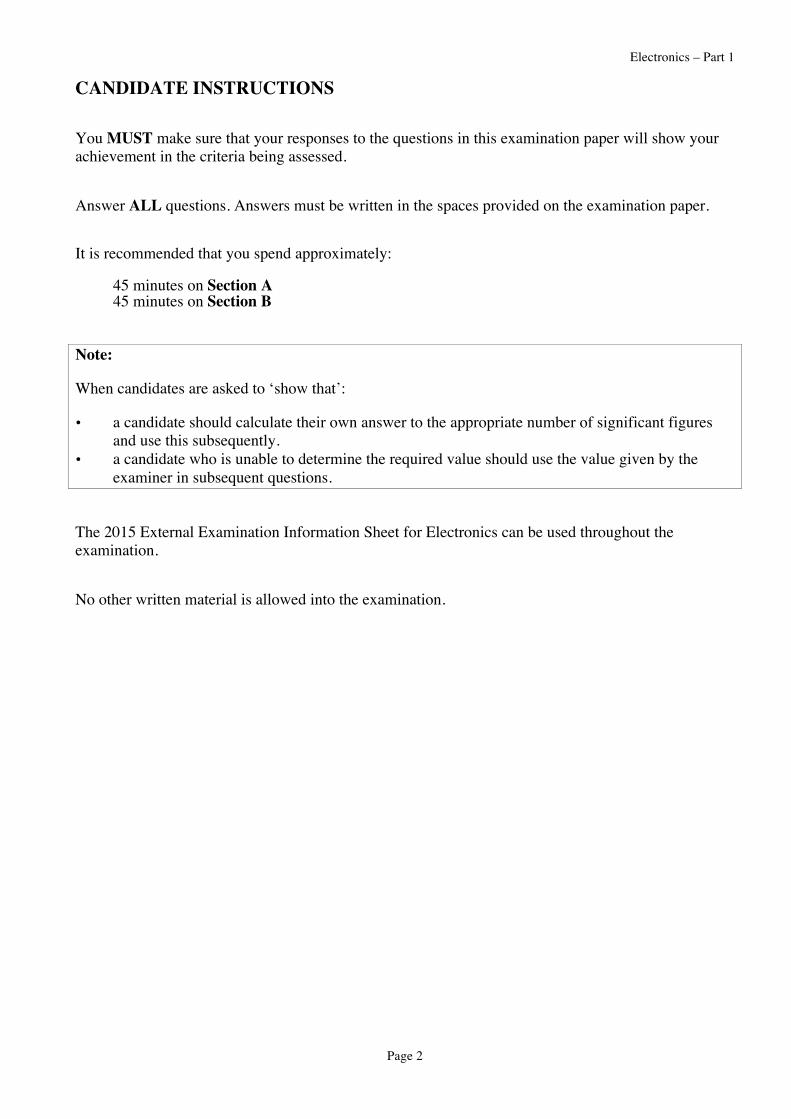
Question 2 In testing an amplifier, a student obtained the following images on a twin-trace oscilloscope. Channel 1 is the input signal and Channel 2 is the output signal. The time base is set to 10 μs/div.
Channel 1
Channel 2
Question 2 continues.
Electronics – Part 1
Page 5
For Marker
Use Only
Question 2 (continued) (a) For the signal, determine: (i) the period (1 mark) .................................................................................................................................... .................................................................................................................................... (ii) the frequency (1 mark) .................................................................................................................................... .................................................................................................................................... (b) Calculate the gain of the amplifier. (2 marks) ............................................................................................................................................. ............................................................................................................................................. .............................................................................................................................................
Question 3 Below are the leg numbers for the PICAXE 08M and a draft design for a simple shed alarm. Diagram 1:
Diagram 2:
(a) Apart from legs 1, 2 and 8, which leg cannot be used as an output? (1 mark) ............................................................................................................................................. (b) Name a leg to which the analogue input could be connected. (1 mark) ............................................................................................................................................. (c) The digital input device is active high and requires that a resistor be connected to the
PICAXE input. On diagram 2, show the required connection of the resistor. (1 mark)
(d) What is the purpose of the resistor in (c) above? (1 mark) ............................................................................................................................................. .............................................................................................................................................
For Marker
Use Only
/4
Electronics – Part 1
Page 7
Question 4 There are occasions when it is desirable to run an op amp amplifier from a single-voltage supply (e.g. a supply of 0 – 12 V). (a) State one advantage and one disadvantage of such a configuration. (2 marks) Advantage: .......................................................................................................................... ............................................................................................................................................. Disadvantage: ..................................................................................................................... ............................................................................................................................................. (b) On the diagram below, sketch an inverting op amp amplifier circuit with a single
voltage supply. (3 marks) (c) The input and output connections need capacitors in series. Show these on the diagram
above and explain their purpose. (2 marks) ............................................................................................................................................. ............................................................................................................................................. ............................................................................................................................................. .............................................................................................................................................
For Marker
Use Only
/7
Electronics – Part 1
Page 8
Question 5 When designing electronic circuits, the correct operation of the circuit must be tested before manufacture. The two main ways would be: using a solderless breadboard and using CAD software. (a) State two reasons for using CAD software to test a circuit. (2 marks) 1. ........................................................................................................................................ ............................................................................................................................................. 2. ........................................................................................................................................ ............................................................................................................................................. (b) Describe two advantages, other than cost, of using a breadboard instead of using CAD
Question 6 (a) Three items of test equipment are: oscilloscope (CRO), logic probe and multimeter.
Suggest a test situation where each would be suitable. (3 marks)
Oscilloscope
Logic probe
Multimeter
(b) A printed circuit board (pcb) is suspected of having a break in one of its tracks. The
diagram below shows the probes of a multimeter used to test the track. (i) State the most suitable function setting for the multimeter to test the pcb. (1 mark) .................................................................................................................................... (ii) With the probes as shown and the multimeter set to the most suitable function, the
display was observed to read 0.00. Explain what this reading indicates about the pcb tracks. (2 marks)
Question 7 The below table may assist you to answer the questions that follow. Trouble-shooting tips from an experienced technician.
1 Visual Inspection
Perform a visual inspection of the unit. Look for any sign of damage (nicks, bent corners) or any indication that the unit was dropped or hit.
2 Foreign Objects Open the unit and look for loose screws, washers, nuts, etc.
3 Burn Components
Look for damage components due to heat (IC, Microprocessors, memories, resistors, etc.).
4 Solder Bridge
Solder bridge can happen with any kind of electronic circuits, but they are more common with Surface Mount circuits. In most cases you will need the aid of a magnify lamp to find it.
5 Cold Solder Joints
Solder Joints are shiny and smooth. If you see any dull solder joint in the section of the board you are working with check it.
6 Blown Fuse Look for blown fuses. Remember diodes can be used as fuses.
7 Crystal Oscillators Crystal Oscillators provide timing for the circuit. So it is a good idea to check the output frequency.
8 Fracture Solder Joints
Fracture solder joints usually happen with time, especially on boards used in the avionics field due to vibration.
9
Missing Components .
I have seen this happen only with Surface Mount circuits, specially units use in avionics (Airplane, Helicopter, etc.) due to vibration, unit been dropped, boards been dropped, etc. So look carefully.
10 Open Traces (PCB Tracks)
Look for this defect. It can save you a lot of time. It happens anytime you have water damage, due to humidity.
11 Overheating Components
Apply power to the unit and touch the top of the component (IC, Microprocessor, Memories, etc.) to see if it is overheating.
12 Wrong Part It happens a lot in the Manufacturing field. 13 Reversed Polarity Very common in the Manufacturing field. 14 Wires Look for wires making intermittent contact.
15 Components Mount on the Board
You will find components mounted on the board using screws, washers, etc. like SCRs, Heatsink specially in Power Supplies. Check them carefully. They can get loose.
16 Software Make sure the unit you are working with has the right
software. Sometimes reloading the software can solve the problem.
(a) Name a circuit problem which is likely to arise from: (2 marks) (i) Foreign object .................................................................................................................................... .................................................................................................................................... (ii) Cold solder joints (dry joint) .................................................................................................................................... ....................................................................................................................................
Question 7 continues.
For Marker
Use Only
Electronics – Part 1
Page 11
Question 7 (continued) (b) Name two procedures which could identify each of: (2 marks) (i) Solder bridge 1. ............................................................................................................................... .................................................................................................................................... 2. ............................................................................................................................... .................................................................................................................................... (ii) Blown fuse 1. ............................................................................................................................... .................................................................................................................................... 2. ............................................................................................................................... .................................................................................................................................... (c) Name two components which could suffer from reversed polarity: (2 marks) 1. ........................................................................................................................................ 2. ........................................................................................................................................ (d) Suggest three reasons a component may overheat. (3 marks) 1. ........................................................................................................................................ ............................................................................................................................................. 2. ........................................................................................................................................ ............................................................................................................................................. 3. ........................................................................................................................................ .............................................................................................................................................
For Marker
Use Only
/9
Electronics – Part 1
Page 12
Question 8 (a) Below is a block diagram for a digital voltmeter. The reasonably steady input voltage is
compared with an increasing voltage from the ramp generator.
(i) What is the purpose of the data latch? (1 mark) .................................................................................................................................... .................................................................................................................................... (ii) What is the role of the trigger pulses which feed into three other blocks? (1 mark) .................................................................................................................................... ....................................................................................................................................
Question 8 continues.
For Marker
Use Only
Electronics – Part 1
Page 13
Question 8 (continued) (b) You are asked to adapt the block diagram for a digital voltmeter shown in (a) to construct
an electronic speedometer for a bicycle. (i) What alterations or additions would you need to make? (2 marks) .................................................................................................................................... .................................................................................................................................... .................................................................................................................................... .................................................................................................................................... (ii) Show the alterations/additions on the original block diagram reproduced below. (2 marks)
For Marker
Use Only
/6
Electronics – Part 1
Page 14
This section assesses Criterion 4. Answer ALL questions from this section. Question 9 (a) Complete this table of capacitor values: (2 marks)
pF Code nF µF
470
223
0.15
3n9
(b) From the following calculated resistor values, determine the closest E12 value and give
its colour code. (3 marks)
Resistor Value Closest E12 Value Colour Code of E12 resistor
51R
258 600 Ω
(c) Three capacitors, 1.5µ, 220n and 470n are given. Arrange two of these capacitors to
give: (2 marks) (i) Maximum total capacitance (ii) Minimum total capacitance
SECTION B
For Marker
Use Only
/7
Electronics – Part 1
Page 15
For Marker
Use Only
Question 10
I
II
III
(a) What is the expected voltage reading in I? (1 mark) ............................................................................................................................................. (b) How does the voltage reading change in II and III? [Note: only approximate values
required, no calculations are needed.] (2 marks) II ............................................................................................................................... volts III .............................................................................................................................. volts (c) Explain how you arrived at your two answers for part (b). (2 marks) ............................................................................................................................................. ............................................................................................................................................. ............................................................................................................................................. .............................................................................................................................................
/5
Electronics – Part 1
Page 16
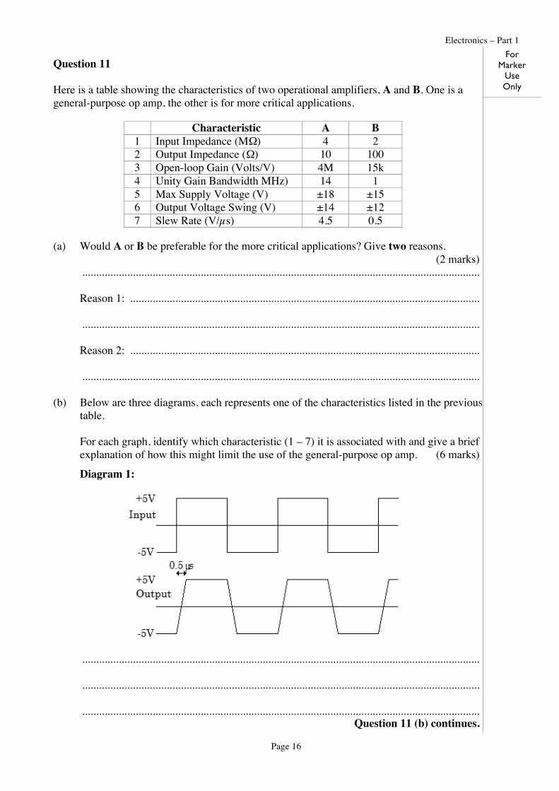
Question 11 Here is a table showing the characteristics of two operational amplifiers, A and B. One is a general-purpose op amp, the other is for more critical applications. (a) Would A or B be preferable for the more critical applications? Give two reasons. (2 marks) ............................................................................................................................................. Reason 1: ............................................................................................................................ ............................................................................................................................................. Reason 2: ............................................................................................................................ ............................................................................................................................................. (b) Below are three diagrams, each represents one of the characteristics listed in the previous
table. For each graph, identify which characteristic (1 – 7) it is associated with and give a brief
explanation of how this might limit the use of the general-purpose op amp. (6 marks)
Question 12 The operational amplifier (op amp) is a type of differential amplifier. (a) Explain the meaning of the term ‘differential amplifier’. (1 mark) ............................................................................................................................................. ............................................................................................................................................. ............................................................................................................................................. (b) What is the input impedance of an ‘ideal’ op amp? (1 mark) ............................................................................................................................................. (c) An AC voltage (as shown on the graph below) is fed into the following op amp circuit.
On the same axes, sketch the expected output voltage for the time shown. Assume the
op amp to be ‘ideal’. (3 marks)
For Marker
Use Only
/5
Time
Electronics – Part 1
Page 19
Question 13 A high-pass filter with a cut-off frequency of 50 Hz has an input signal of 5.0 V and a variable frequency. At high frequencies, 100 mW of power is delivered from the filter. (a) Sketch a labelled Vout ~ frequency graph for this filter showing all relevant features. (2 marks) (b) At the cut-off frequency, determine the following:
(i) The output voltage (1 mark) .................................................................................................................................... ....................................................................................................................................
(ii) The output power (1 mark) .................................................................................................................................... ....................................................................................................................................
For Marker
Use Only
/4
Electronics – Part 1
Page 20
Question 14 A block diagram for a J-K flip-flop and its truth table are show below. (a) Complete the Q (output) column of the table above. (1 mark) (b) Explain carefully how the function of J and K inputs differ from the function of S and R
Question 14 (continued) Below is a circuit diagram for a binary ripple up-counter.
(c) In what mode is each flip-flop operating? (1 mark) ............................................................................................................................................. ............................................................................................................................................. (d) How many output states are possible? (1 mark) ............................................................................................................................................. ............................................................................................................................................. (e) How can you tell that it is a ripple counter and not a synchronous counter? (1 mark) ............................................................................................................................................. ............................................................................................................................................. ............................................................................................................................................. (f) Complete this (partial) timing diagram for the counter. (2 marks)
CLK
Q0
Q1
/8
For Marker
Use Only
Electronics – Part 1
Page 22
Question 15 The diagram below represents a step-down transformer to be used as part of a power supply. The input voltage is 240 Vrms, the output is 12 Vrms. The output from the transformer (Va) is shown in the first graph.
(a) The primary coil of the transformer has 1000 turns. How many turns are in the
Question 15 (continued) A diode is then added to the circuit as shown below.
(b) On the second axes opposite, sketch the expected output voltage pattern, Vb, from this
circuit. (1 mark) (c) The diode was then replaced by a full-wave (bridge) rectifier. (i) On the third axes opposite, sketch the expected output voltage, Vc, when a bridge
rectifier is used. (1 mark) (ii) Sketch the required diode configuration on the circuit diagram below. (2 marks)
(d) To obtain a steady DC output, smoothing is required. Add the required component, with
a typical value, to the circuit above. (1 mark) (e) Modern power supplies often use a switched-mode design. The frequency of the input
voltage is increased electronically before the voltage is transformed. Explain why running at a higher frequency enables a more compact construction. (2 marks) ............................................................................................................................................. ............................................................................................................................................. ............................................................................................................................................. .............................................................................................................................................
/8
For Marker
Use Only
240V rms Vb
240V rms
Vc
Electronics – Part 1
Page 24
This question paper and any materials associated with this examination (including answer booklets, cover sheets, rough note paper, or information sheets) remain the property of the Office of Tasmanian Assessment, Standards and Certification.
Copyright for part(s) of this examination may be held by individuals and/or organisations other than the Office of Tasmanian Assessment, Standards and Certification.
PLACE LABEL HERE
Tasmanian Certificate of Education
ELECTRONICS
Senior Secondary
Subject Code: ELT315114
External Assessment
2015
Time: approximately 90 minutes
On the basis of your performance in this examination, the examiners will provide a result on the following criteria taken from the course statement: Criterion 5 Apply knowledge of digital and analogue systems in describing the function and
operation of components and circuits. Criterion 7 Apply knowledge and understanding of mathematical concepts in electronics.
Section Total C5 C7
PART 2
Electronics – Part 2
Page 2
BLANK PAGE
Electronics – Part 2
Page 3
CANDIDATE INSTRUCTIONS You MUST make sure that your responses to the questions in this examination paper will show your achievement in the criteria being assessed. Answer ALL questions. Answers must be written in the spaces provided on the examination paper. It is recommended that you spend approximately: 45 minutes on Section A 45 minutes on Section B Note: When candidates are asked to ‘show that’: • a candidate should calculate their own answer to the appropriate number of significant figures
and use this subsequently. • a candidate who is unable to determine the required value should use the value given by the
examiner in subsequent questions. The 2015 External Examination Information Sheet for Electronics can be used throughout the examination. No other written material is allowed into the examination.
Electronics – Part 2
Page 4
This section assesses Criterion 5. Answer ALL questions from this section. Question 16 Consider the logic array below.
(a) Complete the logic table for the array shown above. (2 marks)
(b) Describe the condition which makes C low, then write a Boolean expression for the array. (2 marks)
Question 16 (continued) (c) For the input waveforms A and B below, complete the expected output at C in the grid
below. (1 mark)
/5
A
B
C
Electronics – Part 2
Page 6
For Marker
Use Only
Question 17 The diagram for a CR series circuit is shown below. (a) At what time was the switch closed? (1 mark) ............................................................................................................................................. ............................................................................................................................................. (b) The combination has a time constant of approximately 0.2 s. Show that the resistor has
an approximate value of 13 kΩ. (1 mark) ............................................................................................................................................. ............................................................................................................................................. (c) Suppose the resistor were replaced by a resistor of twice the value. On the graph above,
show the expected curve for the new combination. (1 mark)
Question 17 continues.
Electronics – Part 2
Page 7
For Marker
Use Only
Question 17 (continued) (d) A square wave is fed into the CR combination as shown below. The frequency of the
wave is initially 1.0 Hz; it is then increased to 100 Hz. On the graphs below, sketch the expected output voltage patterns for each of the inputs.
(3 marks)
Vin
1.0 Hz
Vin
100 Hz
/6
Electronics – Part 2
Page 8
Question 18 The circuit diagram for an electronic filter is shown below. The input Voltage is 12 Vrms.
(a) Is the filter shown above a high-pass, low-pass or band-pass? Justify your answer. (2 marks) ............................................................................................................................................. ............................................................................................................................................. .............................................................................................................................................
............................................................................................................................................. (b) Is the filter shown above an Active or a Passive filter? Explain. (1 mark) ............................................................................................................................................. ............................................................................................................................................. (c) What effect would increasing the value of the 1.2k resistor have on the circuit? (1 mark) ............................................................................................................................................. .............................................................................................................................................
(d) Given that, in the Pass region, Vout/Vin = 3, what can you conclude about RA and RB? (2 marks) ............................................................................................................................................. ............................................................................................................................................. ............................................................................................................................................. ............................................................................................................................................. (e) What is the output rms voltage at the cut-off frequency? (1 mark) ............................................................................................................................................. .............................................................................................................................................
For Marker
Use Only
/7
Electronics – Part 2
Page 9
Question 19 Below is a design for a cat feeder based on the PICAXE 08M. When the cat steps on a pressure mat, a motor is activated, via a relay, for three seconds to release some food.
PICAXE 08M
Circuit Diagram
(a) On circuit diagram above, label the PICAXE with appropriate Leg Numbers. (1 mark) (b) What is the role of the diode in the circuit diagram? (2 marks) ............................................................................................................................................. ............................................................................................................................................. ............................................................................................................................................. .............................................................................................................................................
For Marker
Use Only
/3
+V
Serial In
In4 / Out4 / ADC4
In3 / Infrain
0V
Out0 / Serial Out
In1 / Out1 / ADC1
In2 / Out2 ADC2
PUSH SWITCH
+5V
10K
3V
0V 0V
DIODE
BC 488 MOTOR RELEASES FOOD PI
CAXE
M
Electronics – Part 2
Page 10
Question 20 A pump control for a solar water heater is being designed. This comparator circuit is part of the design. Two components have not yet been placed in the circuit.
The characteristics of the LDR are shown below. Note: The scales on the axes are not linear
The pump motor is to switch on when the light intensity rises above 150 lux. (a) What is the resistance of the LDR when the light intensity is 150 lux? (1 mark) ............................................................................................................................................. ............................................................................................................................................. (b) What should the output voltage (Vout) be when the light intensity is 200 lux? Explain. (2 marks) ............................................................................................................................................. ............................................................................................................................................. ............................................................................................................................................. .............................................................................................................................................
Question 20 continues.
For Marker
Use Only
Vout
R1
20k
Electronics – Part 2
Page 11
For Marker
Use Only
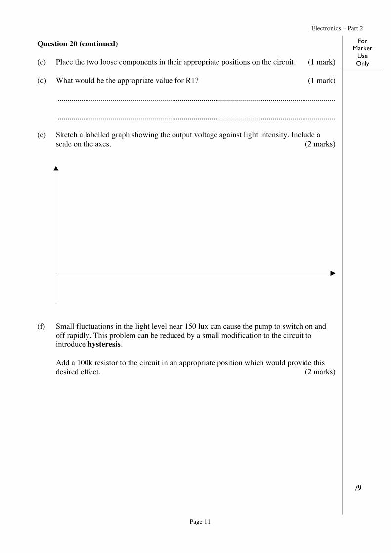
Question 20 (continued) (c) Place the two loose components in their appropriate positions on the circuit. (1 mark) (d) What would be the appropriate value for R1? (1 mark) ............................................................................................................................................. ............................................................................................................................................. (e) Sketch a labelled graph showing the output voltage against light intensity. Include a
scale on the axes. (2 marks) (f) Small fluctuations in the light level near 150 lux can cause the pump to switch on and
off rapidly. This problem can be reduced by a small modification to the circuit to introduce hysteresis.
Add a 100k resistor to the circuit in an appropriate position which would provide this
desired effect. (2 marks)
/9
Electronics – Part 2
Page 12
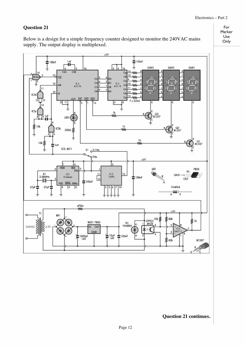
Question 21 Below is a design for a simple frequency counter designed to monitor the 240VAC mains supply. The output display is multiplexed.
Question 21 continues.
For Marker
Use Only
Electronics – Part 2
Page 13
For Marker
Use Only
Question 21 (continued) (a) What is the role of the 100nF component between IC1 and IC2? (1 mark) ............................................................................................................................................. ............................................................................................................................................. (b) Are the displays Common Anode or Common Cathode? Justify your answer. (1 mark) ............................................................................................................................................. ............................................................................................................................................. (c) How would you describe IC3 (upper left of diagram)? (1 mark) ............................................................................................................................................. ............................................................................................................................................. (d) What logic function does IC3d perform as connected in the diagram? (1 mark) ............................................................................................................................................. ............................................................................................................................................. (e) In what mode is IC6 (bottom right corner of diagram) operating? (1 mark) ............................................................................................................................................. ............................................................................................................................................. (f) What is the shape of the signal from Pin 7 of IC6? (1 mark) ............................................................................................................................................. .............................................................................................................................................
Question 21 continues.
Electronics – Part 2
Page 14
For Marker
Use Only
Question 21 (continued)
Diagram repeated
Question 21 continues.
Electronics – Part 2
Page 15
For Marker
Use Only
Question 21 (continued) (g) By considering the LED in OPTO1, what is the purpose of the 470R resistor? (1 mark) ............................................................................................................................................. .............................................................................................................................................
(h) What is the function of IC2? (1 mark) ............................................................................................................................................. ............................................................................................................................................. (i) What is the meaning of the term multiplexing? (2 marks) ............................................................................................................................................. ............................................................................................................................................. ............................................................................................................................................. ............................................................................................................................................. (j) What is the advantage of using multiplexing for the display? (1 mark) ............................................................................................................................................. .............................................................................................................................................
/11
Electronics – Part 2
Page 16
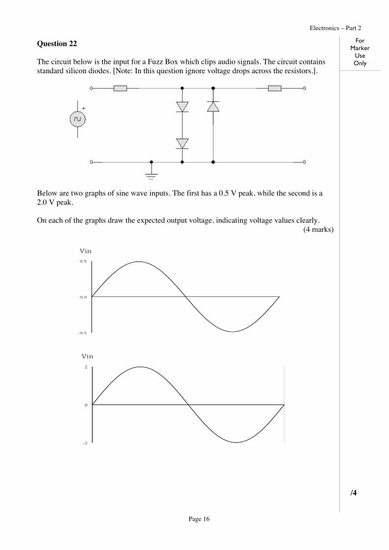
Question 22 The circuit below is the input for a Fuzz Box which clips audio signals. The circuit contains standard silicon diodes. [Note: In this question ignore voltage drops across the resistors.].
Below are two graphs of sine wave inputs. The first has a 0.5 V peak, while the second is a 2.0 V peak. On each of the graphs draw the expected output voltage, indicating voltage values clearly. (4 marks)
For Marker
Use Only
/4
Electronics – Part 2
Page 17
BLANK PAGE
Electronics – Part 2
Page 18
This section assesses Criterion 7. Answer ALL questions from this section. Question 23 In this question, you must show your working. (a) Convert 10710 to octal. (2 marks) ............................................................................................................................................. ............................................................................................................................................. ............................................................................................................................................. ............................................................................................................................................. (b) Add A316 to 1C16 and express your answer in binary. (2 marks) ............................................................................................................................................. ............................................................................................................................................. ............................................................................................................................................. .............................................................................................................................................
/4
SECTION B
For Marker
Use Only
Electronics – Part 2
Page 19
For Marker
Use Only
Question 24 The two-stage amplifier shown below has an input voltage of 6.0 mV (rms) and is required to produce an output voltage of 12.0 V (rms). The input and output impedances for each stage of this amplifier are 1.0 kΩ.
(a) Show that the overall power gain of this amplifier is approximately 66 dB. (2 marks) ............................................................................................................................................. ............................................................................................................................................. ............................................................................................................................................. ............................................................................................................................................. (b) The first stage has a power gain of 42 dB. Calculate the output voltage of stage 1. (2 marks) ............................................................................................................................................. ............................................................................................................................................. ............................................................................................................................................. ............................................................................................................................................. (c) Find the power gain, in dB, of the second stage. (2 marks) ............................................................................................................................................. ............................................................................................................................................. ............................................................................................................................................. ............................................................................................................................................. (d) Calculate the rms power delivered to a 1.0 kΩ load. (2 marks) ............................................................................................................................................. ............................................................................................................................................. ............................................................................................................................................. ............................................................................................................................................. /8
Electronics – Part 2
Page 20
For Marker
Use Only
Question 25
(a) Calculate the value of C (in nF) which makes the rms voltage across C equal to the rms
voltage across the resistor. (2 marks) ............................................................................................................................................. ............................................................................................................................................. ............................................................................................................................................. ............................................................................................................................................. ............................................................................................................................................. ............................................................................................................................................. (b) What is the value of this voltage? (2 marks) ............................................................................................................................................. ............................................................................................................................................. ............................................................................................................................................. ............................................................................................................................................. (c) Why does VR + VC not equal Vin? (2 marks) ............................................................................................................................................. ............................................................................................................................................. ............................................................................................................................................. ............................................................................................................................................. /6
Electronics – Part 2
Page 21
For Marker
Use Only
Question 26 Consider this circuit:
(a) Calculate the resonant frequency of this circuit. (2 marks) ............................................................................................................................................. ............................................................................................................................................. ............................................................................................................................................. ............................................................................................................................................. (b) What is the impedance of this circuit at the resonant frequency? (1 mark) ............................................................................................................................................. ............................................................................................................................................. (c) Determine the reactance of this circuit at 4.0 kHz. (2 marks) ............................................................................................................................................. ............................................................................................................................................. ............................................................................................................................................. ............................................................................................................................................. ............................................................................................................................................. ............................................................................................................................................. (d) Find the impedance of the circuit at 4.0 kHz. (2 marks) ............................................................................................................................................. ............................................................................................................................................. ............................................................................................................................................. .............................................................................................................................................
/7
Electronics – Part 2
Page 22
For Marker
Use Only
Question 27 Below is a circuit diagram for an amplifier based on an op amp.
(a) If Vin = +5.0 V, what will the output voltage be? (1 mark) ............................................................................................................................................. ............................................................................................................................................. A simple Digital-to-Analog Converter (DAC) is constructed using op amps as shown below. The inputs A, B and C are binary inputs; they can either be LOW (0 V) or HIGH (+5 V).
(b) Determine the output voltage when B is HIGH (i.e. 5 V) while A and C
are LOW (0 V). (1 mark) ............................................................................................................................................. ............................................................................................................................................. (c) What would the output voltage be with A and C HIGH and B LOW? (2 marks) ............................................................................................................................................. ............................................................................................................................................. ............................................................................................................................................. .............................................................................................................................................
Question 27 continues.
Electronics – Part 2
Page 23
For Marker
Use Only
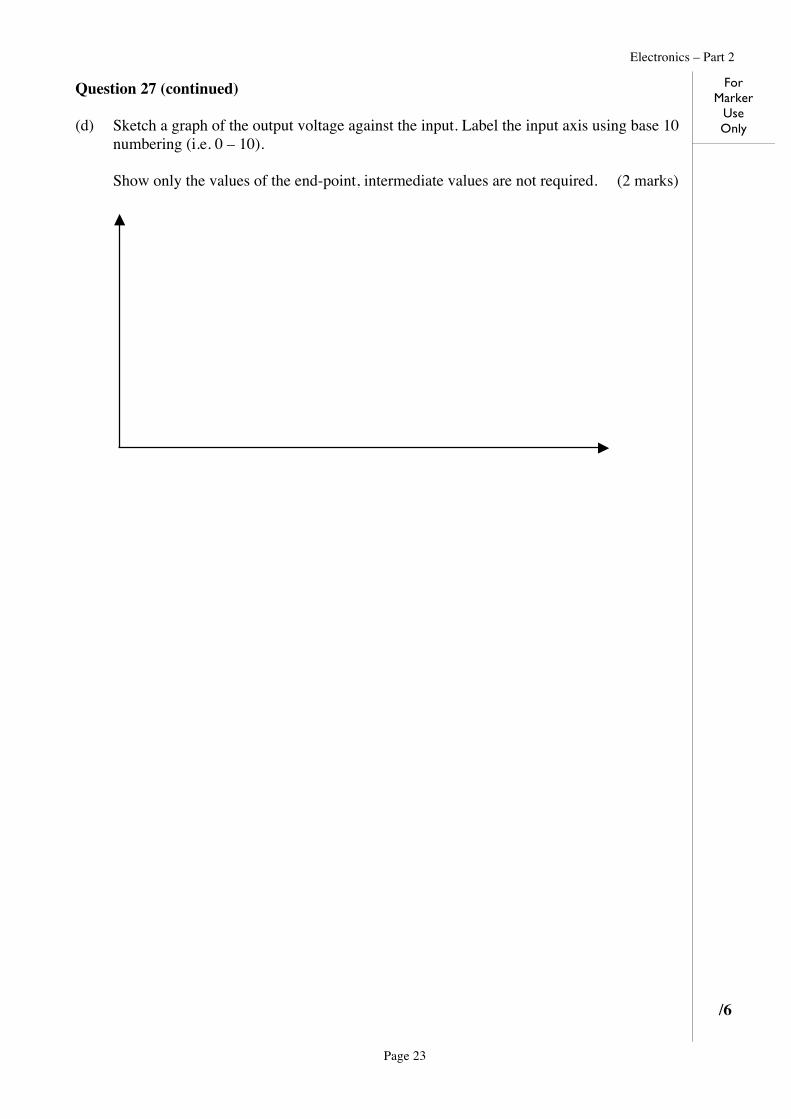
Question 27 (continued) (d) Sketch a graph of the output voltage against the input. Label the input axis using base 10
numbering (i.e. 0 – 10). Show only the values of the end-point, intermediate values are not required. (2 marks)
/6
Electronics – Part 2
Page 24
For Marker
Use Only
Question 28 A simple power supply has an unregulated DC output. Unfortunately there is ripple in the output voltage; the ripple increases as the load current increases.
A simple regulator can be constructed with a zener diode and 100R resistor which will regulate the output voltage (i.e. keep it at a constant voltage of 12 V).
To maintain a constant 12 V across the zener diode, a minimum of 2.0 mA must flow through it. (a) Show that the maximum current which can flow though this 400 mW zener without it
overheating is approximately 30 mA. (1 mark) ............................................................................................................................................. ............................................................................................................................................. (b) Determine the minimum voltage across the resistor when the circuit is properly
stabilised (i.e. when a minimum of 2.0 mA is flowing). (1 mark) ............................................................................................................................................. ............................................................................................................................................. (c) Hence, what is the minimum voltage which must be supplied to the regulator to keep the
Question 28 (continued) (d) When a load is connected and begins to draw current, what happens to the voltage
across the resistor? Explain. (2 marks) ............................................................................................................................................. ............................................................................................................................................. ............................................................................................................................................. ............................................................................................................................................. ............................................................................................................................................. .............................................................................................................................................
/5
Electronics – Part 2
Page 26
BLANK PAGE
Electronics – Part 2
Page 27
For Marker
Use Only
Question 29 An electronics student constructed the following circuit while developing a new traffic light system. IC1 is a 7-bit binary ripple counter; the outputs Q4 – Q6 are labelled A, B and C respectively.
(a) Complete the R, Y and G columns for this truth table for one cycle. [0 = OFF, 1 = ON].
(b) Describe the operation of the yellow light. (2 marks) ............................................................................................................................................. ............................................................................................................................................. ............................................................................................................................................. .............................................................................................................................................
/4
Electronics – Part 2
Page 28
For Marker
Use Only
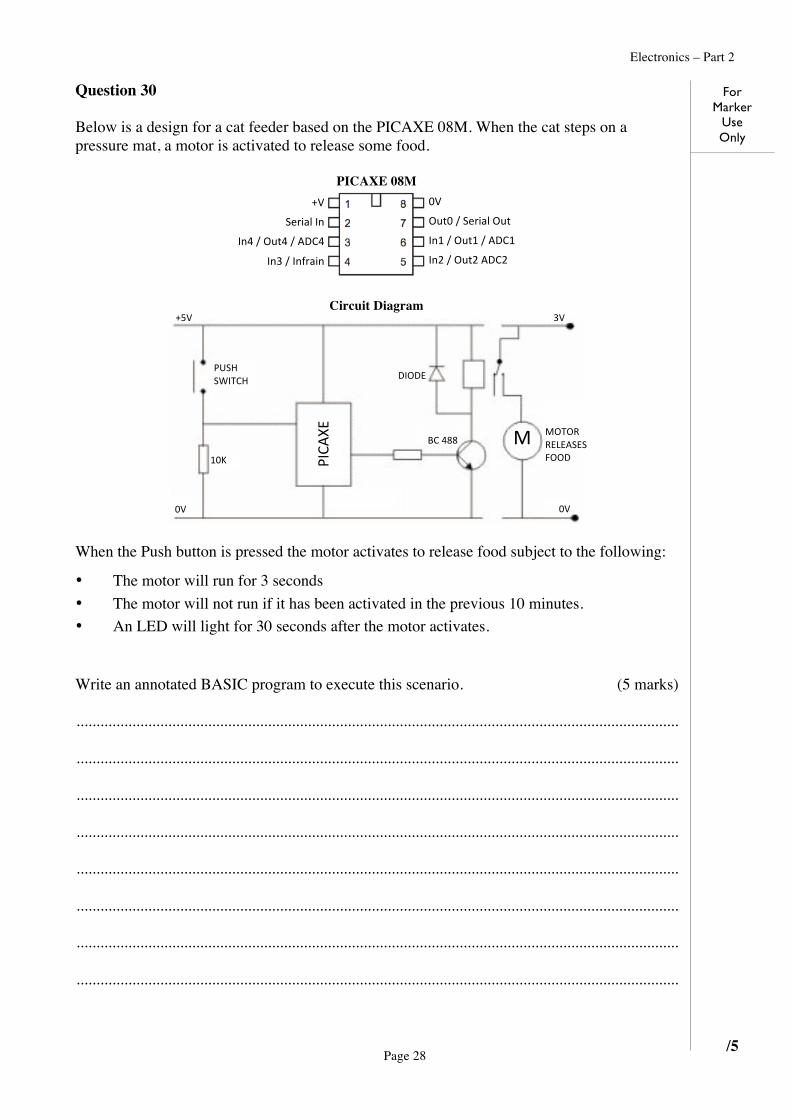
Question 30 Below is a design for a cat feeder based on the PICAXE 08M. When the cat steps on a pressure mat, a motor is activated to release some food.
PICAXE 08M
Circuit Diagram
When the Push button is pressed the motor activates to release food subject to the following:
• The motor will run for 3 seconds • The motor will not run if it has been activated in the previous 10 minutes. • An LED will light for 30 seconds after the motor activates. Write an annotated BASIC program to execute this scenario. (5 marks) ....................................................................................................................................................... ....................................................................................................................................................... ....................................................................................................................................................... ....................................................................................................................................................... ....................................................................................................................................................... ....................................................................................................................................................... ....................................................................................................................................................... .......................................................................................................................................................
/5
+V
Serial In
In4 / Out4 / ADC4
In3 / Infrain
0V
Out0 / Serial Out
In1 / Out1 / ADC1
In2 / Out2 ADC2
PUSH SWITCH
+5V
10K
3V
0V 0V
DIODE
BC 488 MOTOR RELEASES FOOD PI
CAXE
M
Electronics – Part 2
Page 29
BLANK PAGE
Electronics – Part 2
Page 30
BLANK PAGE
Electronics – Part 2
Page 31
BLANK PAGE
Electronics – Part 2
Page 32
This question paper and any materials associated with this examination (including answer booklets, cover sheets, rough note paper, or information sheets) remain the property of the Office of Tasmanian Assessment, Standards and Certification.
Electronics
Subject Code: ELT315114
2015 External Examination Information Sheet
Page 1 of 3
Frequency, period
€
f =1T
Ohm’s Law
€
V = IR,
€
I =VR
, R =VI
Power
€
P =VI , P = I2R, P =V 2
R
Current
€
I =PV
, I =PR
Voltage
€
V = PR
€
V =PI
Resistance
€
R =PI2 , R =
V 2
P
Resistors in series RT = R1 + R2 + R3 + ....
Resistors in parallel 1RT
=1R1
+1R2
+1R3
+ ....
or
€
RT = R1−1 + R2
−1 + R3−1 + ...( )
−1
Capacitors in series 1CT
=1C1
+1C2
+1C3
+ ....
or
€
CT = C1−1 + C2
−1 + C3−1 + ...( )
−1
Capacitors in parallel CT = C1 + C2 + C3 + ....
Inductive reactance XL = 2π f L
Capacitive reactance XC =1
2π f C
RC filter cut off frequency fc =1
2π RC
Impedance ZT = 2R + 2X , X = XL − XC
LC filter resonance
€
f =1
2π LC, C =
1L
. 12πf#
$ %
&
' (
2, L =
1C
. 12πf#
$ %
&
' (
2
RC time constant T RC=
RL time constant TLR
=
Page 2 of 3
Gain
negative gain for an inverting amplifier
€
G =−VoutVin
or
€
−G = RfRin
for a non-inverting amplifier
€
G =VoutVin
or
€
G = 1+RfRin
or
€
G =Rf + RinRin
Summing Amplifier Gain
€
–VoutR f
=Vin1Rin1
+Vin2Rin2
+Vin3Rin3
or
€
Vout = –RfV1R1
+V2R2
+V3R3
"
# $
%
& '
Power Gain(dB)
€
G =10log PoutPin
or
€
20 log Vout
Vinprovided Zin = Zload( )
Peak voltage
€
Vpeak =1.414VRMS RMS voltage
€
VRMS = 0.707Vpeak
Voltage divider
€
Vout =R2
R1 + R2. Vin
Resistor colour code Capacitor value code
Colour digit multiplier tolerance Silver x 0.01 ±10% Gold x 0.1 ±5% Black 0 x 1 Brown 1 x 10 ±1% Red 2 x 100 ±2% Orange 3 x 1000 ±3% Yellow 4 x 10000 ±4% Green 5 x 100000 ±0.5% Blue 6 x 1000000 ±0.25% Violet 7 Grey 8 White 9
First two numerals represent first two digits of capacitor’s value, in picofarads Third numeral represents multiplier (power of 10) e.g. 1000 pF has code 102 10 nF = 10,000 pF has code 103 2.2µF = 2,200,000 pF has code 225