EM SIMULATION USING THE LAGUERRE-FDTD
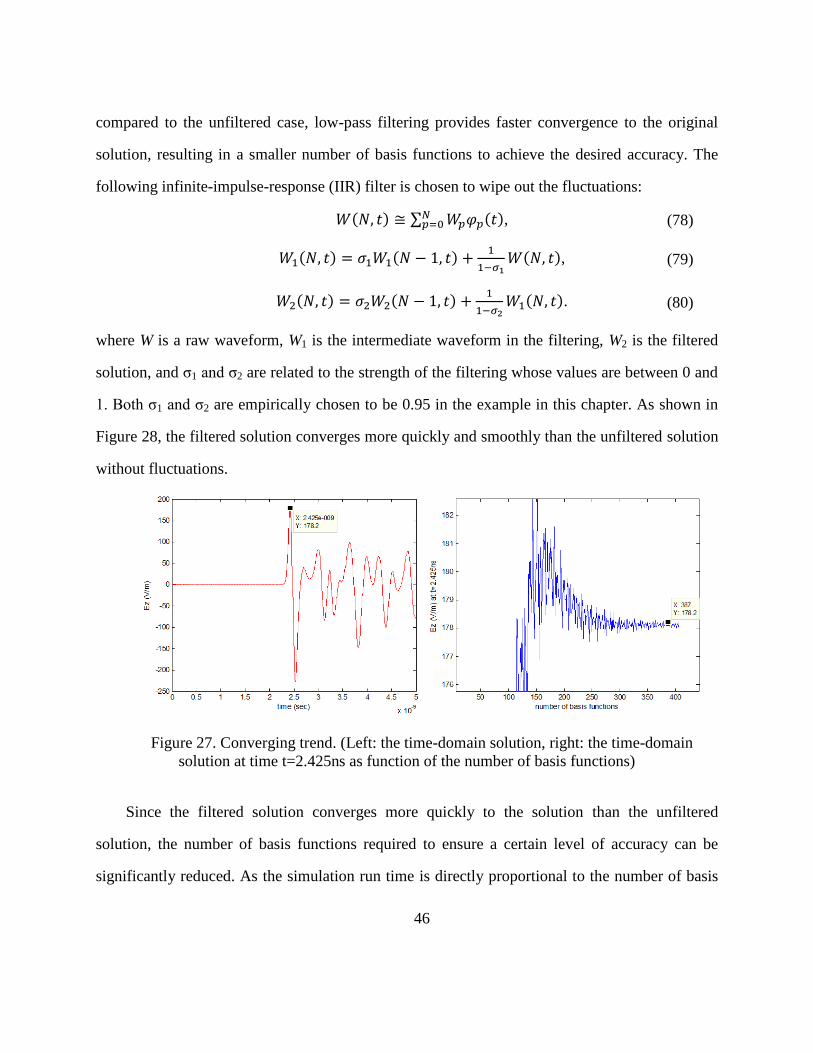
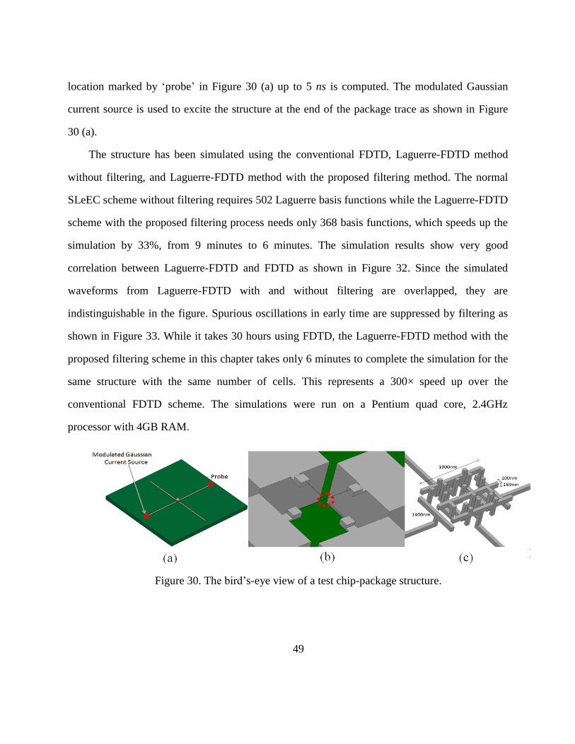
SCHEME FOR MULTISCALE 3-D
INTERCONNECTIONS
A Dissertation
Presented to
The Academic Faculty
By
Myunghyun Ha
In Partial Fulfillment
of the Requirements for the Degree
Doctor of Philosophy in the
School of Electrical and Computer Engineering
Georgia Institute of Technology
December 2011
Copyright © 2011 by Myunghyun Ha
EM SIMULATION USING THE LAGUERRE-FDTD
SCHEME FOR MULTISCALE 3-D
INTERCONNECTIONS
Approved by:
Dr. Madhavan Swaminathan, Advisor
School of Electrical and Computer
Engineering
Georgia Institute of Technology
Dr. Muhannad Bakir
School of Electrical and Computer
Engineering
Georgia Institute of Technology
Dr. Andrew F. Peterson
School of Electrical and Computer
Engineering
Georgia Institute of Technology
Dr. Hao Min Zhou
School of Mathematics
Georgia Institute of Technology
Dr. Manos M. Tentzeris
School of Electrical and Computer
Engineering
Georgia Institute of Technology
Date Approved: Nov. 3, 2011
Dedicated to my parents
iv
ACKNOWLEDGEMENTS
Ten years ago, I was a sophomore and about to choose my major. After long and careful
consideration, I decided to study electrical engineering. Now, I am about to receive the Ph.D.
degree in the electrical and computer engineering, which is the highest academic degree awarded
by universities in the United States. It would not have been possible without the support of many
people. I would like to express my gratitude to the people who inspired and encouraged me.
First of all, I cannot thank my advisor Prof. Madhavan Swaminathan enough for giving me
an invaluable opportunity to work in EPSILON group. Without his continuous trust, guidance
and enthusiasm and encouragement, none of my achievements during my Ph.D. life could be
possible. His insight based on theoretical and industrial background directed my research to the
right way. I would like to thank my committee members, Prof. Andrew F. Peterson, Prof. Manos
M. Tentzeris, Prof. Muhannad Bakir, and Prof. Hao Min Zhou for taking much of their precious
time to give me constructive advice and feedback.
I am forever grateful to Prof. Joungho Kim, my former advisor during my Master‟s degree,
for the opportunity he gave me to be a Tera lab‟s member. The foundation I built with the
experiences and studies in the Tera lab had a strong effect on shaping my ideas. I would like to
thank my manager Dr. Dan Oh and mentor Dr. Joong Ho Kim at Rambus during my summer
internship in 2009 for giving me great opportunities to learn and be inspired.
I was very lucky to have such good people as my colleagues in EPSILON group: Wansuk,
Tae Hong, Lalgudi, Krishna S., Janani, Ranjeeth, Vishal, Sukruth, Aswani, Krishna B., Ki Jin,
Nevin, Abhilash, Nithya, Narayanan, Eddy, Tapo, Suzanne, Jae Young, Jianyong, Kyu, Satyan,
Biancun, Stephen, David, Rishik, Sung Joo, Ming, and Diapa. I would like to thank Suzanne,
Eddy, and Jae Young who joined Tech together in 2007 for having fun and helping each other.
Four years spent with them are priceless to me. I cannot forget weekly MSDT meetings where I
had a lot of helpful discussions with Krishna S., Krishna B., Ki Jin, Jae Young, Narayanan,
v
Ranjeeth, and Bernie. My special thanks go to Krishna S., Ki Jin, Narayanan, Jianyong, and Jae
Young who gave me invaluable discussions on my research ideas. The research faculty of the
EPSILON group has been excellent mentors and I would like to thank Dr. Daehyun Chung, Dr.
Andy Seo, and Dr. Sunghwan Min for constructive discussions.
I can never thank enough to my parents. All of my accomplishments through my life have
been possible by endless loves and unconditional supports from my father, Mr. Jaein Ha, and my
mother, Ms. Soonhye Kim. They provided me the best environment to follow my dream, armed
me with positive attitude, and encouraged me whenever I was in difficult time. I sincerely
appreciate all the gifts from my parents. Therefore, this dissertation is dedicated to my beloved
parents. I wish their health and happiness.
vi
TABLE OF CONTENTS
ACKNOWLEDGEMENTS ................................................................................................. iv
LIST OF TABLES ................................................................................................................. x
LIST OF FIGURES .............................................................................................................. xi
SUMMARY ......................................................................................................................... xvi
CHAPTER I INTRODUCTION .......................................................................................... 1
1.1 BACKGROUND AND MOTIVATION ............................................................................ 1
1.2 CONTRIBUTION ........................................................................................................ 3
1.3 ORGANIZATION OF THE THESIS ................................................................................ 4
CHAPTER II ORIGIN AND HISTORY OF THE PROBLEM ....................................... 6
2.1 NEED FOR 3-D INTEGRATION ................................................................................... 6
2.2 MAJOR ELECTROMAGNETIC DESIGN CHALLENGES .................................................. 8
2.3 CHALLENGES IN TIME-DOMAIN SIMULATION METHOD ........................................... 9
2.3.1 Finite-Difference Time-Domain Method ....................................................................... 9
2.3.2 Alternate Time-Domain Methods ................................................................................. 11
2.4 LAGUERRE-FDTD AND SLEEC METHODOLOGY .................................................... 12
CHAPTER III TRANSIENT SIMULATION USING LAGUERRE POLYNOMIALS
....................................................................................................................................................... 13
3.1 LAGUERRE-FDTD ................................................................................................. 13
3.1.1 Weighted Laguerre Polynomials as Basis Functions.................................................... 13
3.1.2 FDTD with Laguerre Basis Functions .......................................................................... 15
3.1.3 Choice of the Number of Temporal Basis Functions ................................................... 22
3.1.4 Calculation of Electric and Magnetic Fields in Time Domain ..................................... 23
3.2 THE SLEEC ALGORITHM ....................................................................................... 24
vii
3.2.1 Simulation for Long Time Duration ............................................................................. 24
3.2.2 Equivalent-Circuit Model Representation of the FDTD Grid ...................................... 25
3.2.3 Choosing the Correct Number of Basis Functions ....................................................... 31
3.2.4 Node-Numbering Scheme ............................................................................................ 33
3.3 ADVANTAGES OF USING LAGUERRE POLYNOMIALS ............................................... 35
3.4 SUMMARY .............................................................................................................. 37
CHAPTER IV GENERATING THE TIME-DOMAIN WAVEFORM FROM
LIMITED NUMBER OF LAGUERRE BASIS COEFFICIENTS ........................................ 38
4.1 LIMITATIONS OF PRIOR WORK ............................................................................... 38
4.1.1 One Optimal Number of Basis Functions for Multiple Time Points ............................ 41
4.1.2 Spurious Oscillations .................................................................................................... 43
4.2 NEW METHOD FOR OBTAINING ACCURATE TRANSIENT WAVEFORM .................... 45
4.3 NUMERICAL RESULTS ............................................................................................ 48
4.4 SUMMARY .............................................................................................................. 51
CHAPTER V SIMULATION FOR LONG TIME DURATION .................................... 52
5.1 DIFFICULTY IN CALCULATION OF LAGUERRE BASIS FUNCTIONS ........................... 52
5.2 INTRODUCTION OF BALANCED LAGUERRE POLYNOMIAL AND BALANCED
EXPONENTIAL FUNCTION ........................................................................................................... 56
5.3 NUMERICAL RESULTS ............................................................................................ 58
5.4 SUMMARY .............................................................................................................. 60
CHAPTER VI EFFICIENT FREQUENCY-DOMAIN ANALYSIS USING TIME-
DOMAIN SIMULATIONs ......................................................................................................... 61
6.1 TIME-DOMAIN TO FREQUENCY-DOMAIN TRANSFORMATION .................................. 61
6.2 EFFICIENT TIME-DOMAIN SIMULATION FOR FREQUENCY-DOMAIN ANALYSIS ....... 63
6.3 EFFICIENT LAGUERRE-FDTD SIMULATION FOR LOW FREQUENCY ANALYSIS ...... 65
viii
6.4 NUMERICAL RESULTS ............................................................................................ 66
6.5 SUMMARY .............................................................................................................. 69
CHAPTER VII MODELING OF DISPERSIVE AND CONDUCTIVE MATERIAL IN
3-D STRUCTURES .................................................................................................................... 70
7.1 TIME-DOMAIN FORMULATION FOR FREQUENCY-DEPENDENT MATERIALS ............. 70
7.2 TRANSFORMATION OF CONVOLUTION OPERATION FROM TIME-DOMAIN TO
LAGUERRE-DOMAIN ................................................................................................................... 71
7.3 LAGUERRE-DOMAIN FORMULATION FOR FREQUENCY-DEPENDENT MATERIALS ... 73
7.4 CUSTOMIZED FORMULATION FOR DISPERSION MODEL .......................................... 76
7.4.1 Debye model ................................................................................................................. 76
7.4.2 Lorentz model ............................................................................................................... 78
7.5 NUMERICAL RESULTS ............................................................................................ 80
7.6 SUMMARY .............................................................................................................. 83
CHAPTER VIII TEST CASES .......................................................................................... 84
8.1 TSV ARRAY .......................................................................................................... 84
8.1.1 3-by-3 TSV Array ......................................................................................................... 85
8.1.2 5-by-5 TSV Array ......................................................................................................... 87
8.2 TSV-TSV COUPLING ............................................................................................. 90
8.3 MICROSTRIP LINE WITH RETURN PATH DISCONTINUITY ........................................ 94
8.3.1 Simple Microstrip Line ................................................................................................. 95
8.3.2 Microstrip Line over Slot ............................................................................................. 97
8.3.3 Microstrip Line over Small Holes ................................................................................ 99
8.3.4 Importance of Modeling Dispersion ........................................................................... 101
8.4 MICROSTRIP LINE WITH TSV ON SILICON CARRIER ............................................. 105
8.4.1 Microstrip Line with Return Path Discontinuity I ...................................................... 105
8.4.2 Microstrip Line with Return Path Discontinuity II..................................................... 109
ix
8.4.3 Microstrip Line with TSV transition and no Return Current Discontinuity ............... 111
8.5 COMPLEXITY SCALING ......................................................................................... 113
8.6 SUMMARY ............................................................................................................ 114
CHAPTER IX CONCLUSION ........................................................................................ 116
9.1 CONTRIBUTION .................................................................................................... 116
9.1.1 Generating time-domain waveforms from solutions in Laguerre domain .................. 116
9.1.2 Simulation for Long Time Intervals ........................................................................... 117
9.1.3 Frequency-domain Analysis Method using Laguerre-FDTD ..................................... 117
9.1.4 Modeling of Dispersive and Conductive Materials .................................................... 117
9.2 PUBLICATIONS ( FROM THIS WORK) .................................................................... 118
9.3 PUBLICATIONS ( FROM PAST WORK) .................................................................... 119
CHAPTER X FUTURE WORK ...................................................................................... 120
10.1 MODELING OF NONLINEAR PHENOMENA ............................................................. 120
10.2 MODELING OF SKIN EFFECT ................................................................................. 120
APPENDIX A: DERIVATION OF COMPLETE 3-D MODEL OF SLEEC .............. 122
APPENDIX B: MATHEMATICAL JUSTIFICATION FOR ERROR ANALYSIS AT
THE INITIAL POINT .............................................................................................................. 133
APPENDIX C: SLeEC SOFTWARE .............................................................................. 137
APPENDIX D: LAGUERRE-FDTD FORMULATION FOR VARIOUS BOUNDARY
CONDITIONS ........................................................................................................................... 168
REFERENCES .................................................................................................................. 170
VITA ................................................................................................................................... 174
x
LIST OF TABLES
Table 1. Selected orthogonal polynomials. ........................................................................... 36
Table 2. Memory consumption of general and customized formulation for Debye model. . 81
Table 3. Summary of test cases ........................................................................................... 115
Table 4. Configuration of SLeEC software. ........................................................................ 137
xi
LIST OF FIGURES
Figure 1. 3-D multi-functional vertical integration in semiconductor packages. (Courtesy:
Interconnect and Package Center, Georgia Institute of Technology.) ............................................ 2
Figure 2. Flow chart of a software tool „SLeEC‟ .................................................................... 4
Figure 3. An estimate of system-integration density driven by package-based technology [1].
......................................................................................................................................................... 7
Figure 4. Typical multilayer stack-ups used/proposed for electronic packages. (Courtesy:
Packaging Research Center, Georgia Institute of Technology.) ..................................................... 8
Figure 5. Multiscale features in a chip-package structure. .................................................... 10
Figure 6. Laguerre basis functions for orders p = 0 to p = 4. ................................................ 15
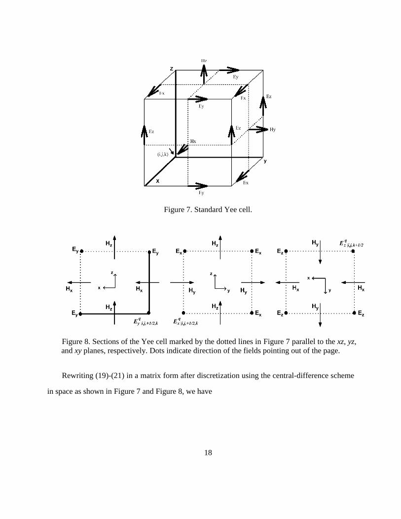
Figure 7. Standard Yee cell. .................................................................................................. 18
Figure 8. Sections of the Yee cell marked by the dotted lines in Figure 7 parallel to the xz, yz,
and xy planes, respectively. Dots indicate direction of the fields pointing out of the page. ......... 18
Figure 9. The total simulation time divided into different intervals...................................... 25
Figure 10. Standard Yee cell. ................................................................................................ 26
Figure 11. Sections of the Yee cell marked by the dotted lines in Figure 10 parallel to the xz,
yz, and xy planes, respectively. Dots indicate direction of the fields pointing out of the page. .... 26
Figure 12. Companion model of the 3-D FDTD grid in Laguerre domain. .......................... 28
Figure 13. Energy content as a function of the number of basis functions. .......................... 32
Figure 14. Efficient node-numbering scheme. ...................................................................... 34
Figure 15. Sparsity pattern of the A matrix suitable for LU decomposition. ........................ 35
Figure 16. Example time-domain waveform to be recovered using Laguerree basis functions.
....................................................................................................................................................... 39
Figure 17. Energy content of the recovered waveform as a function of the number of basis
functions. ....................................................................................................................................... 40
xii
Figure 18. Error at t = 0 as a function of the number of basis functions. .............................. 40
Figure 19. Recovered time-domain waveform using 162 basis functions compared with
original waveform. ........................................................................................................................ 41
Figure 20. Comparison of the recovered time-domain waveforms near t = 4.6 ns. .............. 42
Figure 21. Comparison of the recovered time-domain waveforms near t = 4.35 ns. ............ 42
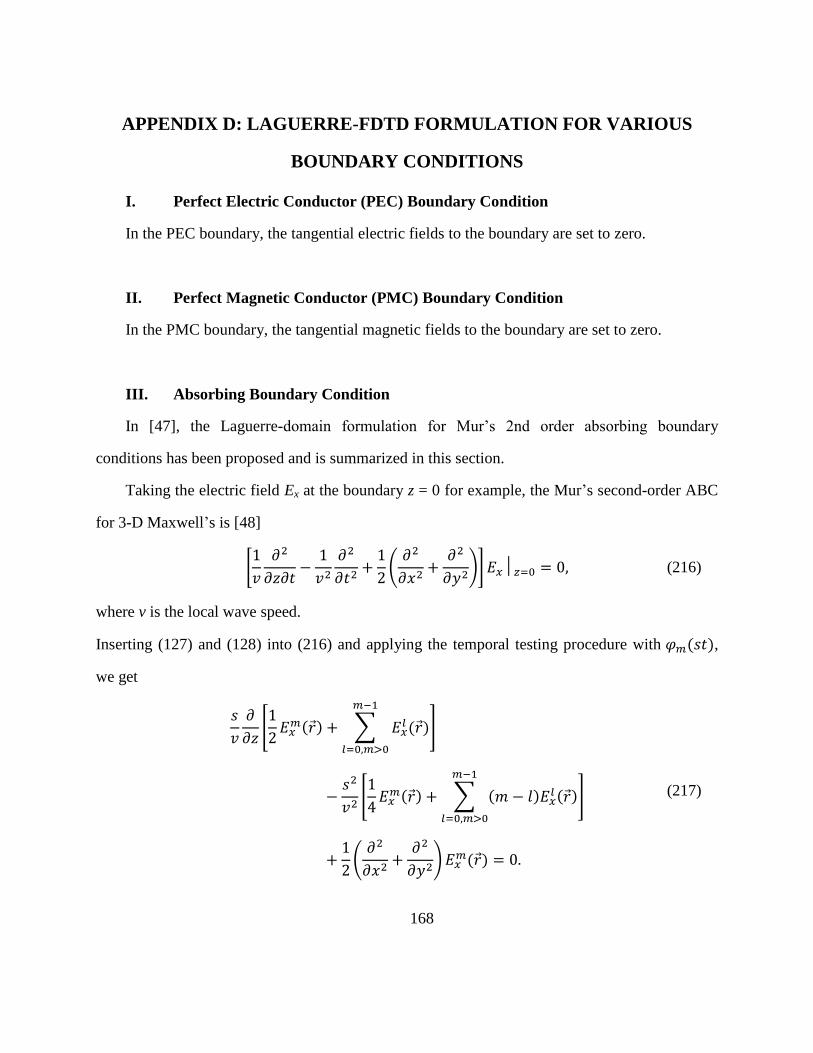
Figure 22. Spurious oscillations. (Left: Recovered time-domain waveform, right: magnified
view of the circled area) ................................................................................................................ 43
Figure 23. Example waveform to recover ............................................................................. 43
Figure 24. Recovered waveform using 500 basis functions. ................................................. 44
Figure 25. Recovered waveform using 5000 basis functions. ............................................... 44
Figure 26. Recovered waveform using 50000 basis functions. ............................................. 45
Figure 27. Converging trend. (Left: the time-domain solution, right: the time-domain
solution at time t=2.425ns as function of the number of basis functions) .................................... 46
Figure 28. Convergence of the filtered solution. ................................................................... 47
Figure 29. Removal of spurious oscillations by filtering. ..................................................... 48
Figure 30. The bird‟s-eye view of a test chip-package structure. ......................................... 49
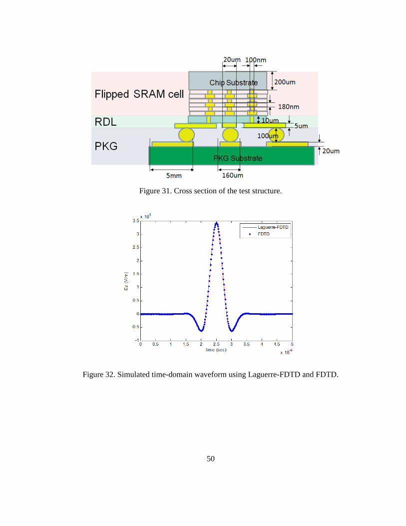
Figure 31. Cross section of the test structure. ....................................................................... 50
Figure 32. Simulated time-domain waveform using Laguerre-FDTD and FDTD. ............... 50
Figure 33. Reduction of spurious oscillations in early time. ................................................. 51
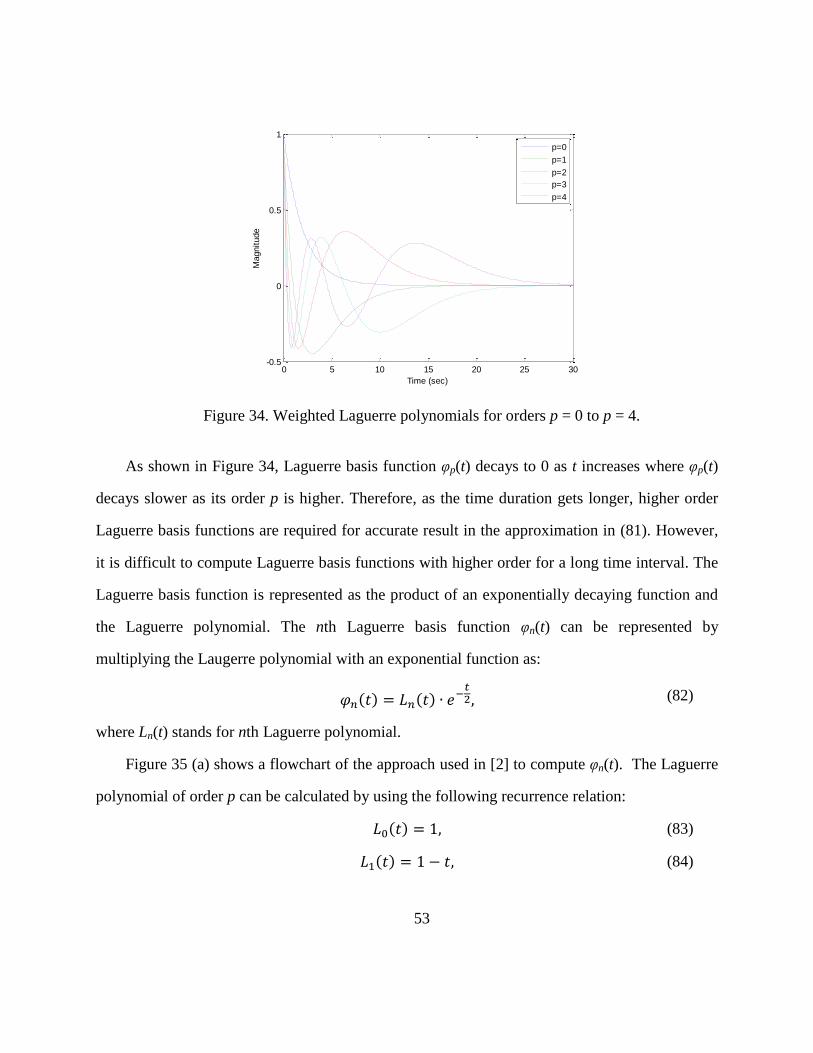
Figure 34. Weighted Laguerre polynomials for orders p = 0 to p = 4. .................................. 53
Figure 35. Algorithm to compute the Laguerre basis function. (a): algorithm in the prior
work, (b): proposed algorithm ...................................................................................................... 55
Figure 36. Calculated 1000th Laguerre basis function by the prior method. ........................ 55
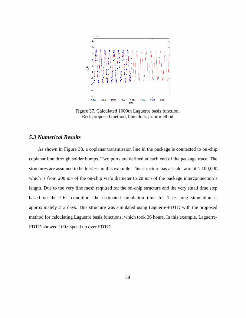
Figure 37. Calculated 1000th Laguerre basis function. ......................................................... 58
Figure 38. Coplanar transmission line structure from PKG to chip. ..................................... 59
Figure 39. Simulated time-domain waveform at Port 1. ....................................................... 59
xiii
Figure 40. Insertion loss (s21) of the coplanar transmission line structure. .......................... 60
Figure 41. Two-port network. ............................................................................................... 62
Figure 42. Two-port network with additional resistances at port locations. ......................... 64
Figure 43. 2.4GHz band-pass filter. (top: cross-sectional view, bottom: top view of the
layout of the M0 layer. Dots are separated by 50 um) .................................................................. 67
Figure 44. Oscillatory transient response. ............................................................................. 68
Figure 45. Rapidly decaying transient response. ................................................................... 68
Figure 46. Calculated S parameters. ...................................................................................... 69
Figure 47. Test structure: Microstrip transmission line......................................................... 80
Figure 48. Simulated time-domain waveforms. .................................................................... 82
Figure 49. Comparison between simulated time-domain waveforms with dispersive and non-
dispersive FR-4 model. ................................................................................................................. 82
Figure 50. 3-by-3 TSV array. (left: top view, right: side cross-sectional view).................... 85
Figure 51. Ports definition on TSV array. ............................................................................. 86
Figure 52. Discretization of circular cross section of TSV. .................................................. 86
Figure 53. Calculated S parameters of 3-by-3 TSV array. .................................................... 87
Figure 54. 5-by-5 TSV array. ................................................................................................ 88
Figure 55. Calculated S parameters of 5-by-5 TSV array. .................................................... 89
Figure 56. Categorization of TSVs in 5-by-5 TSV array using symmetry. .......................... 90
Figure 57. TSV-TSV coupling test vehicle. .......................................................................... 91
Figure 58. Meshing of test vehicle. ....................................................................................... 92
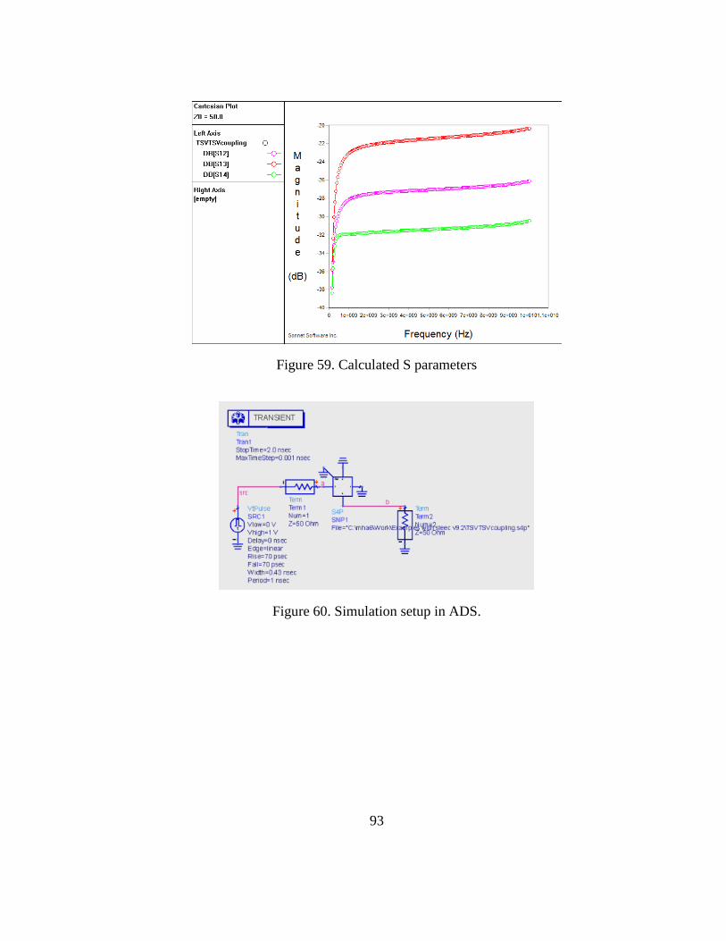
Figure 59. Calculated S parameters ....................................................................................... 93
Figure 60. Simulation setup in ADS...................................................................................... 93
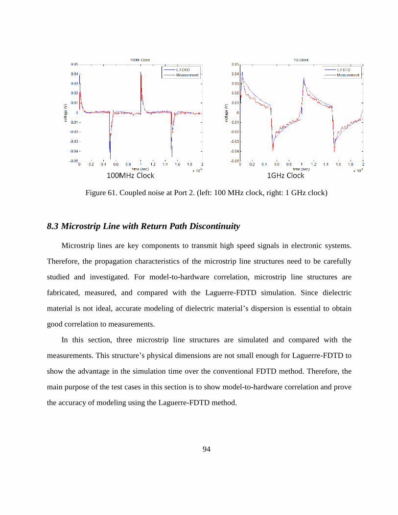
Figure 61. Coupled noise at Port 2. (left: 100 MHz clock, right: 1 GHz clock) ................... 94
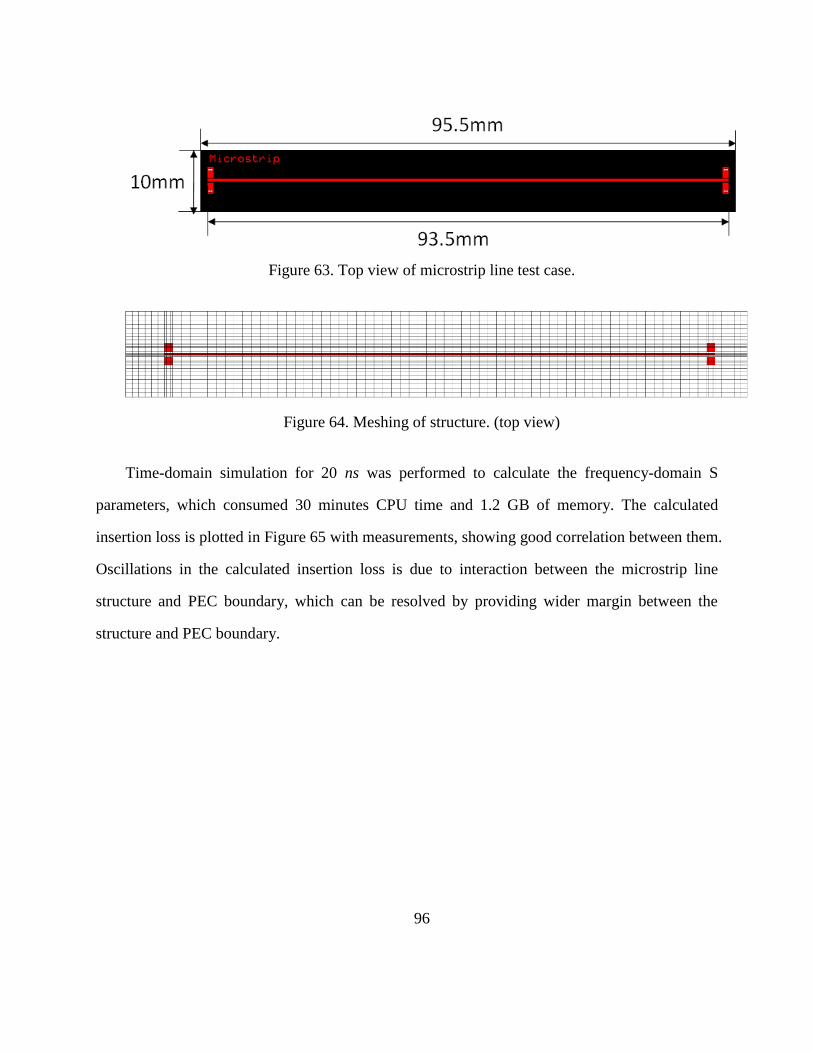
Figure 62. Side cross-sectional view of microstrip line test case. ......................................... 95
Figure 63. Top view of microstrip line test case. .................................................................. 96
xiv
Figure 64. Meshing of structure. (top view) .......................................................................... 96
Figure 65. Calculated and measured insertion losses of microstrip-line test case. ............... 97
Figure 66. Top view (top) and side cross-sectional view (bottom) of test case. ................... 98
Figure 67. Meshing of structure. (top view) .......................................................................... 98
Figure 68. Calculated and measured insertion losses of the microstrip-line-over-a-slot test
case. ............................................................................................................................................... 99
Figure 69. Top view (top) and side cross-sectional view (bottom) of test case. ................. 100
Figure 70. Meshing of structure. (top view) ........................................................................ 100
Figure 71. Calculated and measured insertion losses of microstrip-line-over-small-holes test
case. ............................................................................................................................................. 101
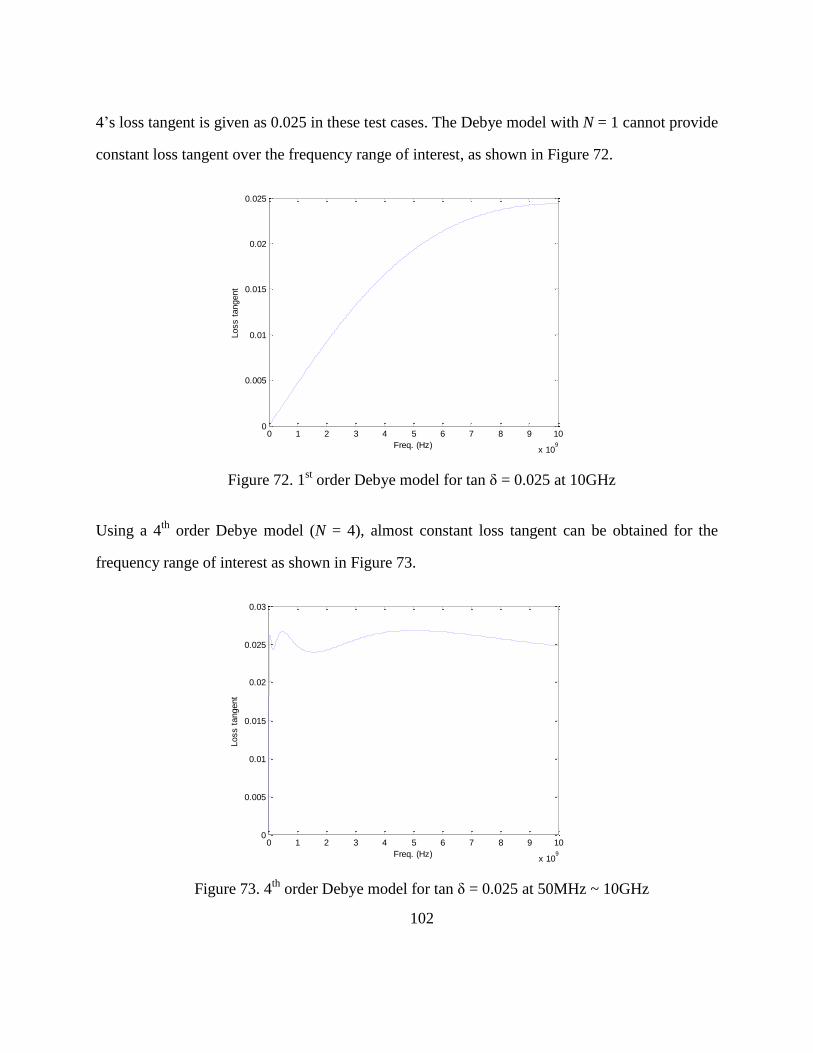
Figure 72. 1st order Debye model for tan δ = 0.025 at 10GHz ............................................ 102
Figure 73. 4th
order Debye model for tan δ = 0.025 at 50MHz ~ 10GHz ........................... 102
Figure 74. Insertion of loss of simple microstrip line using a 1st order Debye model and a 4
th
order Debye model. ..................................................................................................................... 104
Figure 75. Insertion of loss of microstrip line over a slot using a 1st order Debye model and
a 4th
order Debye model. ............................................................................................................. 104
Figure 76. Insertion of loss of microstrip line over small holes using a 1st order Debye model
and a 4th
order Debye model. ...................................................................................................... 105
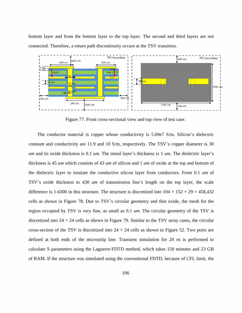
Figure 77. Front cross-sectional view and top view of test case. ........................................ 106
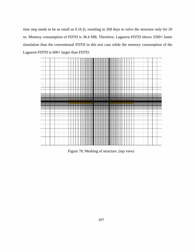
Figure 78. Meshing of structure. (top view) ........................................................................ 107
Figure 79. Discretization of circular cross section of TSV ................................................. 108
Figure 80. Calculated return loss (left) and insertion loss (right). ....................................... 108
Figure 81. Front cross-sectional view and top view of test case. ........................................ 109
Figure 82. Meshing of structure. (top: whole structure, bottom: enlarged view of red-circled
area)............................................................................................................................................. 110
Figure 83. Calculated insertion loss. ................................................................................... 110
xv
Figure 84. Expanded bird‟s-eye view and front cross-sectional view of test case. ............. 111
Figure 85. Lateral mesh near TSVs between second and third metal layer. ....................... 112
Figure 86. Calculated return loss (left) and insertion loss (right). ....................................... 113
Figure 87. The scaling of memory complexity (left) and computational complexity (right).
..................................................................................................................................................... 114
Figure 88. Standard Yee cell. .............................................................................................. 123
Figure 89. Sections of the Yee cell marked by the dotted lines in Figure 7 parallel to the xz,
yz, and xy planes, respectively. Dots indicate direction of the fields pointing out of the page. .. 123
Figure 90. Companion model of the 3-D FDTD grid in Laguerre domain. ........................ 131
Figure 91. Electric fields in the 3-D FDTD grid. ................................................................ 131
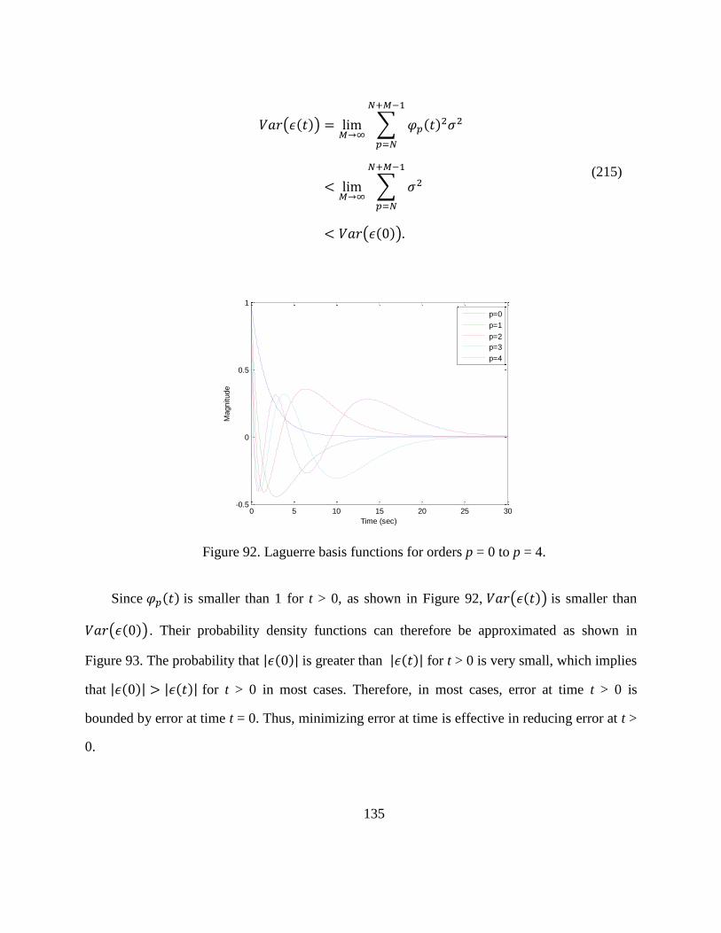
Figure 92. Laguerre basis functions for orders p = 0 to p = 4. ............................................ 135
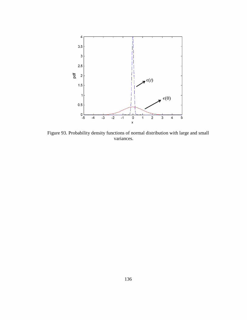
Figure 93. Probability density functions of normal distribution with large and small
variances. .................................................................................................................................... 136
Figure 94. Flow chart of SLeEC software. .......................................................................... 138
xvi
SUMMARY
As the current electronic trend is toward integrating multiple functions in a single electronic
device, there is a clear need for increasing integration density which is becoming more
emphasized than in the past. To meet the industrial need and realize the new system-integration
law [1], three-dimensional (3-D) integration is becoming necessary. 3-D integration of multiple
functional IC chip/package modules requires co-simulation of the chip and the package to
evaluate the performance of the system accurately. Due to large scale differences in the physical
dimensions of chip-package structures, the chip-package co-simulation in time-domain using the
conventional FDTD scheme is challenging because of Courant-Friedrich-Levy (CFL) condition
that limits the time step. Laguerre-FDTD has been proposed to overcome the limitations on the
time step. To enhance performance and applicability, SLeEC methodology [2] has been proposed
based on the Laguerre-FDTD method. However, the SLeEC method still has limitations to solve
practical 3-D integration problems.
This dissertation proposes further improvements of the Laguerre-FDTD and SLeEC method
to address practical problems in 3-D interconnects and 3-D integration. A method that increases
the accuracy in the conversion of the solutions from Laguerre-domain to time-domain is
demonstrated. A methodology that enables the Laguerre-FDTD simulation for any length of time,
which was challenging in prior work, is proposed. Therefore, the analysis of the low-frequency
response can be performed from the time-domain simulation for a long time period. An efficient
method to analyze frequency-domain response using time-domain simulations is introduced.
Finally, to model practical structures, it is crucial to model dispersive materials. A Laguerre-
FDTD formulation for frequency-dependent dispersive materials is derived in this dissertation
and has been implemented.
1
CHAPTER I
INTRODUCTION
1.1 Background and Motivation
In the semiconductor industry, a need for high performance, small size, and low-cost
solutions for functional integration is becoming more significant. To keep up with the industrial
need, three-dimensional (3-D) integration called system-on-package (SoP) as shown in Figure 1
is becoming necessary. As more functionality is integrated into the package, electromagnetic
interactions within the package pose a significant problem. The problem in high-density
integration which includes 3-D structures is the requirement for tools that enable the design and
analysis of package structures and ICs within the package together at the same time, which is
also called “chip-package co-simulation”.
Both chip-package co-simulation and the analysis of 3-D interconnection structures have a
common ground in that there is a large scale difference in the physical dimensions of the
structure to be dealt with. For chip-package co-simulation, structures with a wide range of
physical dimensions from tens of nanometers to a few millimeters need to be considered together.
In 3-D integration, vertical interconnections are realized using through-silicon via (TSV)
interconnections, employing silicon as a new packaging substrate. Use of TSV increases the
integration density considerably. Silicon oxide used as an oxide liner in TSVs plays an important
role in the TSV‟s electrical response. However, the oxide‟s thickness is very thin compared to
the via itself. Therefore, TSV structures fall into the category of multiscale structures. This
dissertation however is not limited to TSVs and addresses any structure that contains a multiscale
geometry.
2
Figure 1. 3-D multi-functional vertical integration in semiconductor packages. (Courtesy:
Interconnect and Package Center, Georgia Institute of Technology.)
Traditional time-domain techniques, such as the finite-difference time-domain method, are
limited by the well-known Courant-Friedrich-Levy (CFL) condition and are not suitable for the
simulation of multiscale problems which arise in high-density integration. The CFL condition
poses an upper bound on the time step to obtain stable simulation results. The CFL limit is
inversely proportional to the smallest mesh dimensions. In the case of the simulation of
multiscale structures, small dimensions in the structure require a very fine mesh, which makes
the time step prohibitively small. An unconditionally stable scheme using Laguerre polynomials,
which is referred to as Laguerre-FDTD, is suggested for simulation of multiscale structures in 3-
D integration as an alternative to FDTD. Because of the Laguerre-FDTD‟s unconditional
stability, the time step in the Laguerre-FDTD is not limited by CFL condition. Therefore, the
Laguerre-FDTD enables significant speed-up in the simulation of multiscale structures arising in
high-density integration.
3
1.2 Contribution
Based on the Laguerre-FDTD, SLeEC methodology has been proposed to enhance the
performance, which will be introduced in detail in CHAPTER III. However, both SLeEC
methodology and Laguerre-FDTD still have difficulties in the application to practical problems.
This dissertation focuses on enhancing the Laguerre-FDTD‟s applicability. The following work
has been completed in this dissertation:
1. An efficient method to recover a time-domain waveform from solutions in the
Laguerre-domain has been proposed.
2. The limited time duration for which the Laguerre-FDTD could be simulated earlier
has been resolved, enabling low-frequency analysis using Laguerre-FDTD.
3. A frequency-domain analysis methodology using the Laguerre-FDTD has been
proposed.
4. A Laguerre-FDTD based formulation for frequency-dependent dispersive materials
has been proposed.
Based on the above contributions, a software tool has been developed that solves
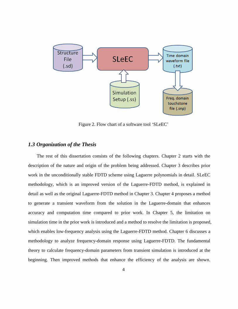
electromagnetic fields in time domain for a given structure and a given source current, which is
called SLeEC. The term „SLeEC‟ comes from SLeEC methodology which is an improved
version of Laguerre-FDTD and will be shown in detail in 3.2. Because the code was initially
developed using the SLeEC methodology and has been upgraded as the research in this
dissertation proceeds, the software tool‟s name is still „SLeEC‟ although improvements made in
this dissertation are not limited to SLeEC methodology, but applicable to general Laguerre-
FDTD. The flow chart in Figure 2 shows how the software tool works. It reads two files
regarding structure description and simulation setup. The software is explained in detail in
Appendix C.
4
Figure 2. Flow chart of a software tool „SLeEC‟
1.3 Organization of the Thesis
The rest of this dissertation consists of the following chapters. Chapter 2 starts with the
description of the nature and origin of the problem being addressed. Chapter 3 describes prior
work in the unconditionally stable FDTD scheme using Laguerre polynomials in detail. SLeEC
methodology, which is an improved version of the Laguerre-FDTD method, is explained in
detail as well as the original Laguerre-FDTD method in Chapter 3. Chapter 4 proposes a method
to generate a transient waveform from the solution in the Laguerre-domain that enhances
accuracy and computation time compared to prior work. In Chapter 5, the limitation on
simulation time in the prior work is introduced and a method to resolve the limitation is proposed,
which enables low-frequency analysis using the Laguerre-FDTD method. Chapter 6 discusses a
methodology to analyze frequency-domain response using Laguerre-FDTD. The fundamental
theory to calculate frequency-domain parameters from transient simulation is introduced at the
beginning. Then improved methods that enhance the efficiency of the analysis are shown.
5
Chapter 7 proposes a Laguerre-FDTD formulation for modeling losses. A mathematical
technique to convert a formulation using frequency-domain information to Laguerre-domain is
introduced. Chapter 8 documents practical 3-D test examples that show model-to-hardware
correlation and correlation to commercial tools. Chapter 9 concludes this dissertation and
summarizes the contributions of this dissertation. Finally, Chapter 10 proposes future work.
6
CHAPTER II
ORIGIN AND HISTORY OF THE PROBLEM
2.1 Need for 3-D integration
Modern electronics require higher computational speed and data bandwidth with a smaller
form factor, which result in an increasing level of transistor integration density in
semiconductors [3] [4]. From the development of integrated circuits (IC) to system-on-chip
(SoC), silicon-based technology has driven the growth of the integration technology. SoC is
increasing the capability for miniaturization of various computing units and memory blocks [5].
However, the extension of the functionality with SoC is limited. Multimedia mobile devices
require various subsystems including analog, radio frequency (RF), and sensor submodules in
addition to digital computing units, and SoC has difficulty in integrating various heterogeneous
subsystems on one single chip. Furthermore, the time-to-market for SoC is not short enough to
meet the rapidly-changing trends of mobile applications [6].
Package-based system integration is an attractive solution for multi-functional integration
for mobile applications. As advanced packaging technology enables the integration of various
submodules in a single package platform, the realization of the multi-functional system becomes
easier. With progress in processing technology, package-based system component densities will
increase, as shown in Figure 3 [1].
7
Figure 3. An estimate of system-integration density driven by package-based technology [1].
For the realization of the new system-integration law, instead of cramming chips on the
planar substrate layout as in traditional multi-chip modules (MCM), the integration of
submodules vertically using 3-D space is employed in such multilayer structures, as shown in
Figure 4. Currently, the 3-D packaging concept is realized through System-in-Package (SiP),
which stacks bare or packaged ICs vertically. System-on-Package (SoP) is a more extensive
architecture of 3-D integration than SiP and contains embedded passives and active components
in a package. For microminiaturization, 3-D integration is the fundamental method being pursued
for today's package-based system integration [7] [8].
8
Figure 4. Typical multilayer stack-ups used/proposed for electronic packages. (Courtesy:
Packaging Research Center, Georgia Institute of Technology.)
2.2 Major Electromagnetic Design Challenges
There are several critical electromagnetic effects that one needs to carefully consider in the
design of SiP or SoP. Those effects can be classified into reflected noise, simultaneous switching
noise (SSN), crosstalk noise, and attenuation [9] [10].
Reflection noise is produced due to impedance mismatch. Incorrect terminations and signal
path discontinuities cause impedance mismatch and result in overshoot, undershoot, and ringing.
Possible sources of impedance mismatch are changes in the signal-trace width, branching of the
signal trace, and signal-line crossing a gap in the reference plane giving rise to return-path
discontinuity. SSN is caused by parasitic inductance of the power-distribution network (PDN).
SSN causes fluctuation in the voltage between power and ground planes, especially when a large
number of devices switch simultaneously. It is because SSN is proportional to the inductance of
the PDN and the first derivative of current flow with respect to time. Crosstalk noise is caused by
the direct electromagnetic coupling between signal traces and vias. The close placement of such
9
structures results in the coupling of electric and magnetic fields, giving rise to mutual
capacitance and mutual inductance, respectively. Attenuation is caused by dielectric dispersion
and conductor loss. Attenuation suppresses the signal‟s amplitude therefore signal-to-noise ratio
(SNR) is degraded. In addition, loss is proportional to the frequency. The high-frequency
component and low-frequency component of a signal are attenuated differently, which results in
signal distortion deteriorating signal integrity.
As more functionality is integrated in a package with higher performance in the 3-D
integration, the electromagnetic interactions within the package become more significant and
complex. Especially, in the case of a mixed-signal system containing digital, analog, and RF
modules, it is critical to fully characterize the system at the design level using an electromagnetic
solver. Therefore, 3-D interconnection design requires engineering solutions for issues that were
not observed earlier in the planar-interconnection design.
2.3 Challenges in Time-Domain Simulation Method
Key features in chip-package structures that need to be addressed in the design of 3-D
integrated systems stem from its multiscale physical dimensions. For chip-package co-simulation,
structures with a wide range of physical dimensions from tens of nanometers to a few
millimeters need to be considered together. In 3-D integration, vertical interconnections are
realized using through-silicon via (TSV) interconnections which also fall into the category of
multiscale structures.
2.3.1 Finite-Difference Time-Domain Method
The finite-difference time-domain (FDTD) scheme is a ubiquitous method for transient
electromagnetic (EM) analysis [11]. The main drawback of FDTD is the Courant-Friedrich-Levy
(CFL) condition, which limits the time step for obtaining stable and accurate simulation results
10
[12]. In EM analysis, smaller mesh dimension contributes to a smaller CFL time step. In
mathematical form, the CFL condition for EM simulation is given by
((
)
(
)
(
)
)
(1)
where vmax is the maximum phase velocity of the wave propagation while Δx, Δy, and Δz are the
smallest mesh dimensions in the x, y, and z directions [12]. The time-step limit for numerical
stability can be derived using dispersion analysis [12].
The CFL condition is a major bottleneck in using FDTD for co-simulation of multiscale
structures. Multiscale dimensions in a chip-package structure are shown in Figure 5. The on-chip
structures are in the nanometer scale, the solder pads typically have a diameter of 50 μm, the
package interconnects are in the 100 μm range, and the package structures, such as the power-
ground planes, are in the mm scale. The on-chip structures that are in the nm range require fine
meshes, making the time step prohibitively small.
Figure 5. Multiscale features in a chip-package structure.
11
2.3.2 Alternate Time-Domain Methods
The multi-resolution time-domain (MRTD) scheme using scaling and wavelet functions has
been shown to provide savings of an order of magnitude with respect to execution time [13]. By
using orthonormal wavelet spatial expansions, the MRTD scheme can reduce the spatial
discretization to two steps per wavelength. However, the stability condition for MRTD becomes
more stringent [14]. Hollands‟ method proposed in [15] has been used to reduce the simulation
time by avoiding fine meshing for thin wires, by modeling the thin wires with a cell size smaller
than the FDTD cell. The MRTD and Holland method are not applicable to general structures
arising in high-density integration.
To eliminate the CFL stability condition, implicit methods can be used. These implicit
techniques, in particular, alternating-direction-implicit (ADI) methods, have been used in solving
heat transfer problems [16], followed by various unconditionally stable finite-difference
formulations for parabolic equations [17]. Such implicit techniques were introduced into the
FDTD schemes for solving Maxwell‟s equations, resulting in an implicit unconditionally stable
ADI–FDTD method [18]. The ADI-FDTD scheme can be used to speed up simulation and has
been shown to provide a 10× improvement in the simulation time [19]. A rigorous theoretical
proof of the unconditional stability was presented with numerical verifications in [20]. Due to the
removal of the CFL conditions in the ADI-FDTD method, the time step is no longer restricted by
the stability conditions, but by the modeling accuracy of the algorithm. One of the factors that
affect the accuracy is numerical dispersion. In [21], it has been shown that using a time step
larger than the CFL limit results in increased numerical dispersion in the ADI-FDTD based
method.
Recently, based on the time-domain finite element method (FEM), the time-domain finite
element reduction recovery (FE-RR) method has been proposed [22]. The time-domain FE-RR
method has an advantage of linear complexity, which is suitable to solve very large scale and
12
complex problems. The time-domain FE-RR method has been improved to have unconditional
stability by employing unconditionally stable time-domain differencing schemes [23]. However,
since the time-domain FE-RR method is a marching-on-time scheme, similar to ADI-FDTD, the
author believes that larger time-step then CFL limit may introduce computational error even
though the stability of the simulation is maintained.
2.4 Laguerre-FDTD and SLeEC methodology
Laguerre-FDTD and SLeEC methodologies have been proposed to overcome the limitation
on the time step in the conventional FDTD. They use Laguerre polynomials to ensure
unconditional stability of the simulation and are explained in detail in CHAPTER III. However,
they still have limitations when used to solve the practical 3-D integration problems, e.g., the
difficulty to obtain the low-frequency response and to treat frequency-dependent material
properties. For the Laguerre polynomial based methods to be applicable to practical problems, it
is crucial to resolve these limitations, which motivated this research.
13
CHAPTER III
TRANSIENT SIMULATION USING LAGUERRE POLYNOMIALS
Laguerre-FDTD can be significantly faster than FDTD and other time-domain methods
especially for packaging problems containing multiscale dimensions. By using an implicit-
solution technique, a decrease in simulation time has been achieved at the expense of an increase
in memory consumption. More importantly, because of the Laguerre-FDTD‟s unconditional
stability, the time-step limitation has been removed. Since the Laguerre-FDTD is a marching-on-
time scheme, a time step larger than Courant-Friedrich-Levy (CFL) limit does not deteriorate the
accuracy of the simulation. In contrast, other methods such as ADI-FDTD [18] suffer from
numerical dispersion when the time-step is larger than the CFL limit [21].
3.1 Laguerre-FDTD
An unconditionally stable implicit-FDTD scheme using Laguerre polynomials has been
proposed in [24]. The method presented in [24] is referred to as the Laguerre-FDTD scheme in
this dissertation. The Laguerre-FDTD is an unconditionally stable scheme and therefore, the time
step is not limited by the CFL condition. In [24], it has been shown that the Laguerre-FDTD can
be 80 to 100 times faster than the conventional FDTD scheme where a marching-on-time method
is used to update the electromagnetic fields. Because of the unconditional stability of the
transient simulation using Laguerre polynomials and the use of an implicit computational method,
the author believes that the Laguerre-FDTD method is ideally suited for the simulation of
multiscale structures arising in chip-package co-design.
3.1.1 Weighted Laguerre Polynomials as Basis Functions
Consider the set of polynomials defined by
14
( )
( ) (2)
( ) is the Laguerre polynomial of order p. Note that the Laguerre polynomials are causal,
which means that they are defined for time . The Laguerre polynomials satisfy a recursive
relationship given by
( ) , (3)
( ) , (4)
( ) ( ) ( ) ( ) ( ) . (5)
The Laguerre polynomials are orthogonal with respect to the weighting function :
∫ ( ) ( )
(6)
where is the Kronecker delta. Therefore, an orthonormal set of basis functions
can be derived from (6) as follows:
( ) ( ) (7)
where s > 0 is a time-scale factor. These basis functions are referred to as the Laguerre basis
functions. The Laguerre basis functions are also orthogonal with respect to the scaled time
variable , which can be expressed as
∫ ( ) ( )
, (8)
where . In (8), is the time multiplied by the time-scale factor s. The Laguerre basis
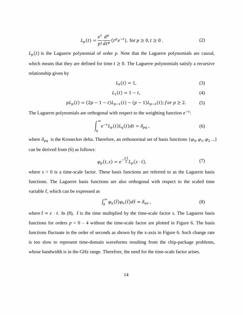
functions for orders p = 0 – 4 without the time-scale factor are plotted in Figure 6. The basis
functions fluctuate in the order of seconds as shown by the x-axis in Figure 6. Such change rate
is too slow to represent time-domain waveforms resulting from the chip-package problems,
whose bandwidth is in the GHz range. Therefore, the need for the time-scale factor arises.
15
Note that the Laguerre basis functions converge to zero as t ∞. Therefore, arbitrary
functions spanned by these basis functions also converge to zero as t ∞, which means that any
function consisting of Laguerre basis functions is unconditionally stable.
Figure 6. Laguerre basis functions for orders p = 0 to p = 4.
3.1.2 FDTD with Laguerre Basis Functions
Consider the following three of six Maxwell‟s differential equations [12]:
(
) (9)
(
) (10)
(
) (11)
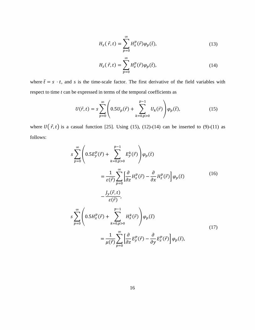
Using the Laguerre basis functions, the temporal coefficients for the electric and magnetic fields
in (9)-(11) can be expanded as
( ) ∑ ( ) ( )
(12)
0 5 10 15 20 25 30-0.5
0
0.5
1
Time (sec)
Magnitude
p=0
p=1
p=2
p=3
p=4
16
( ) ∑ ( ) ( )
(13)
( ) ∑ ( ) ( )
(14)
where , and s is the time-scale factor. The first derivative of the field variables with
respect to time t can be expressed in terms of the temporal coefficients as
( ) ∑( ( ) ∑ ( )
)
( ) (15)
where ( ) is a casual function [25]. Using (15), (12)-(14) can be inserted to (9)-(11) as
follows:
∑( ( ) ∑
( )
)
( )
( )∑ [
( )
( )] ( )
( )
( )
(16)
∑( ( ) ∑
( )
)
( )
( )∑ [
( )
( )] ( )
(17)
17
∑( ( ) ∑
( )
)
( )
( )∑ [
( )
( )] ( )
(18)
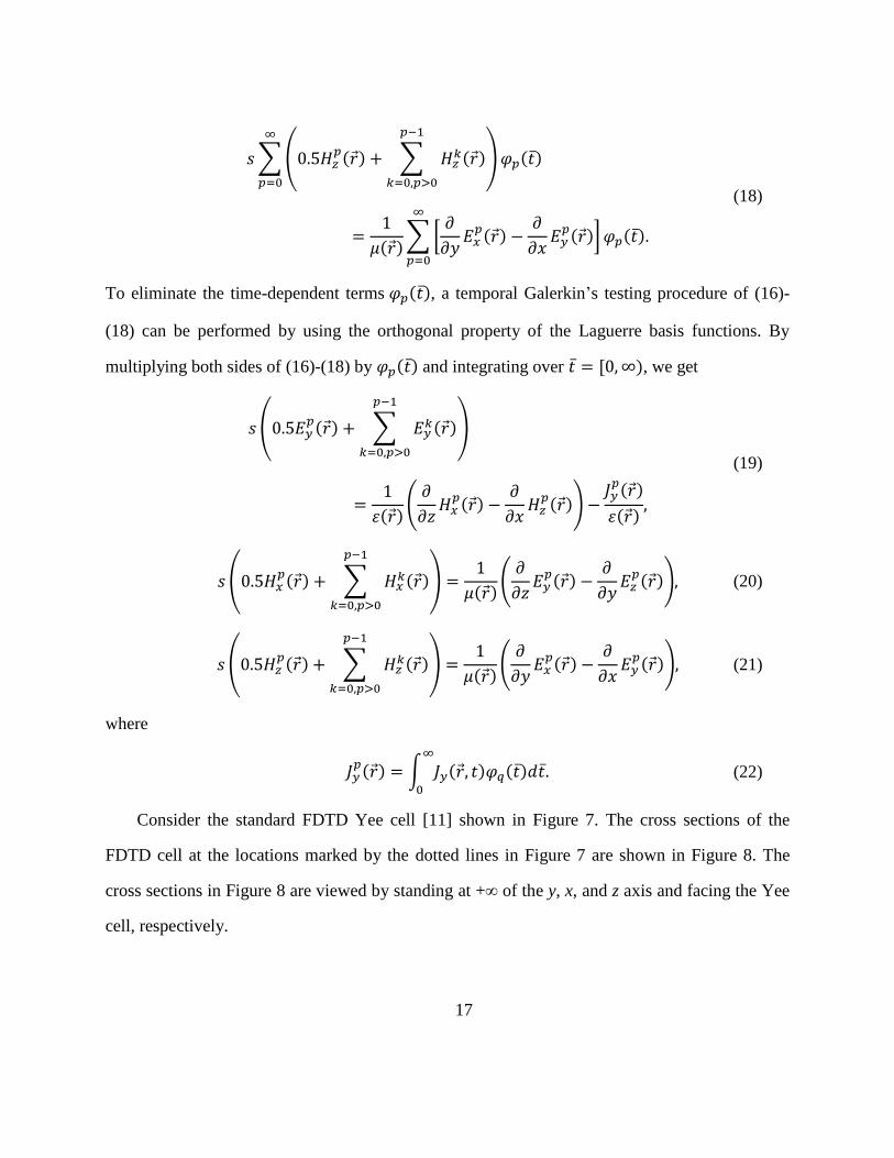
To eliminate the time-dependent terms ( ), a temporal Galerkin‟s testing procedure of (16)-
(18) can be performed by using the orthogonal property of the Laguerre basis functions. By
multiplying both sides of (16)-(18) by ( ) and integrating over , ), we get
( ( ) ∑
( )
)
( )(
( )
( ))
( )
( )
(19)
( ( ) ∑
( )
)
( )(
( )
( )) (20)
( ( ) ∑
( )
)
( )(
( )
( )) (21)
where
( ) ∫ ( ) ( )
(22)
Consider the standard FDTD Yee cell [11] shown in Figure 7. The cross sections of the
FDTD cell at the locations marked by the dotted lines in Figure 7 are shown in Figure 8. The
cross sections in Figure 8 are viewed by standing at +∞ of the y, x, and z axis and facing the Yee
cell, respectively.
18
Figure 7. Standard Yee cell.
Figure 8. Sections of the Yee cell marked by the dotted lines in Figure 7 parallel to the xz, yz,
and xy planes, respectively. Dots indicate direction of the fields pointing out of the page.
Rewriting (19)-(21) in a matrix form after discretization using the central-difference scheme
in space as shown in Figure 7 and Figure 8, we have
19
(
)
(
)
∑
(23)
(
)
(
)
∑
(24)
(
)
(
)
∑
(25)
where
(26)
(27)
(28)
(29)
20
(30)
Inserting (24) and (25) into (23) and rewriting (23), we have
(31)
where
(32)
(33)
(34)
(35)
(36)
(37)
21
(38)
(39)
(40)
(41)
(42)
(43)
(44)
∑
∑
∑
∑
(45)
In (31),
has a relationship with the adjacent 12 electric fields. Equations for the
electric fields in the x and z directions can be derived in a similar fashion. In (31), the magnetic
fields are known because their orders are lower than those of the electric fields. Therefore,
equations for the electric fields can be written as a matrix equation as follows:
, -* + * + * + , (46)
22
where
* +
, (47)
* +
. (48)
In (46), * + is the summation term from order 0 to q – 1. In addition, * + represents the
excitation current source, which is a known vector. Therefore, the Laguerre coefficients for the
electric fields * + can be calculated recursively using (46) from order q = 0.
Contrary to the conventional FDTD method, the Laguerre-FDTD has an implicit
relationship between the field variables, which results in a sparse system matrix [A]. This system
matrix [A] is independent of the order q of the temporal-testing function ( ). Therefore, after
the LU decomposition of [A] is performed at the beginning of the computations, (46) can be
solved by using the back-substitution routine repeatedly.
By using the Laguerre basis functions which decay as t ∞, the stability is no longer
affected by the time-step size. The time step is used only to calculate the Laguerre coefficients of
the excitation in (22) at the beginning of the computations. Therefore, choosing a small time step
does not increase the compute time.
3.1.3 Choice of the Number of Temporal Basis Functions
The method to choose the number of basis functions introduced in [24] is explained in this
section. Consider a real time-domain signal P(t) which is defined over the range [0, Tf] and is
band-limited up to a frequency B. P(t) can be represented by a Fourier series as follows:
( ) ∑
(49)
where
. Since P(t) is real,
where * means conjugate transpose. If P(t) is band-
limited to B Hz, then the value of u can be fixed by
23
. (50)
Therefore, we have
( ) ∑
(51)
In (57), there are 2BTf+1 terms in the expansion of P(t). From this, [24] concludes that at least
2BTf+1 terms of the Laguerre series are required to completely characterize the time-domain
waveform of duration Tf and bandwidth 2B, irrespective of its shape.
3.1.4 Calculation of Electric and Magnetic Fields in Time Domain
By solving (46) recursively, the coefficients of each Laguerre basis function can be obtained,
which are the expansion coefficients of the electric and magnetic fields. From (12)-(14), we
obtain
( ) ∑
( )
(52)
( ) ∑
( )
(53)
( ) ∑
( )
(54)
As shown in Figure 6, the Laguerre basis functions ( ) decays to zero as . Therefore,
the electric and magnetic fields obtained from (52)-(54) also decay to zero as .
24
3.2 The SLeEC Algorithm
Since the introduction of the Laguerre-FDTD methodin [24], several modifications have
been made to the algorithm for enhancing its performance [2]. In [2], an equivalent-circuit model
of the FDTD grid has been developed. This method has been applied to both electromagnetic and
circuit problems consisting of inductors, resistors and capacitors in [26]. The modified algorithm
has been named SLeEC which stands for “Simulation using Laguerre Equivalent Circuit.”
The following modifications and additions to the original Laguerre-FDTD scheme have
been made in the SLeEC algorithm [27].
1. The limited time duration for which Laguerre-FDTD could be simulated has been
resolved, so that Laguerre-FDTD can be done for all time duration (to capture the fast
and slow transients up to DC).
2. The companion model for the FDTD grid has been developed, making the
implementation easier without the use of long cumbersome equations.
3. A numerical method by which the correct number of basis coefficients is chosen has
been proposed to obtain maximum accuracy.
4. A node numbering scheme for optimal memory efficiency has been suggested.
Each of these modifications is explained in detail in the following sections.
3.2.1 Simulation for Long Time Duration
A major drawback of the Laguerre-FDTD in [24] is that the transient simulation can be
performed only for a limited time duration. The reason is the difficulty in the calculation of the
Laguerre basis functions for long time and high order, which will be explained in detail in
CHAPTER V.
In the SLeEC method, the limitation is overcome by dividing the total simulation time into
different intervals [2]. Let Interval 1 span from time t = t0 to t = t1, Interval 2 span from time t =
25
t1 to t = t2, and so on, as shown in Figure 9. The length of each interval is chosen such that
simulation can be accurately performed in the time duration. The final values at the end of
Interval i are used as initial conditions to simulate in Interval (i + 1). This process is repeated
until the time duration for which the simulation needs to be done is completed. The companion
models for FDTD simulation include initial conditions to enable restarting a simulation, which
will be shown in the following subsection. The differential equations that describe the transient
behavior of a system have been modified to explicitly include initial conditions that will permit
simulation for all time duration. The SLeEC algorithm is applied in each of the time intervals.
Figure 9. The total simulation time divided into different intervals.
3.2.2 Equivalent-Circuit Model Representation of the FDTD Grid
The Laguerre-FDTD approach requires solving a system of linear equations of the form Ax
= b to obtain the unknown Laguerre basis coefficients. In the SLeEC method, the linear
equations on FDTD grid are replaced by equivalent companion models composed of resistors,
voltage-controlled current sources and independent current sources. The equivalent-circuit
models enable the use of the stamping rule [28] used in modified nodal analysis [29] to generate
and solve the matrix equation, thereby making the implementation easier [30]. Spice [31]
simulators, in general, use the modified-nodal-analysis method for simulation. Therefore, the
SLeEC method can be seamlessly integrated into Spice for transient EM simulations using
Laguerre polynomials.
In the Laguerre-FDTD method, Maxwell‟s differential equations of the FDTD grid are
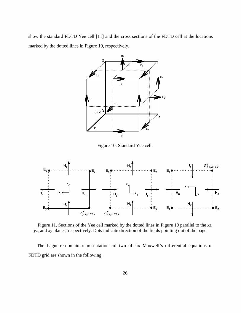
converted into the Laguerre domain as shown in the previous section. Figure 10 and Figure 11
26
show the standard FDTD Yee cell [11] and the cross sections of the FDTD cell at the locations
marked by the dotted lines in Figure 10, respectively.
Figure 10. Standard Yee cell.
Figure 11. Sections of the Yee cell marked by the dotted lines in Figure 10 parallel to the xz,
yz, and xy planes, respectively. Dots indicate direction of the fields pointing out of the page.
The Laguerre-domain representations of two of six Maxwell‟s differential equations of
FDTD grid are shown in the following:
27
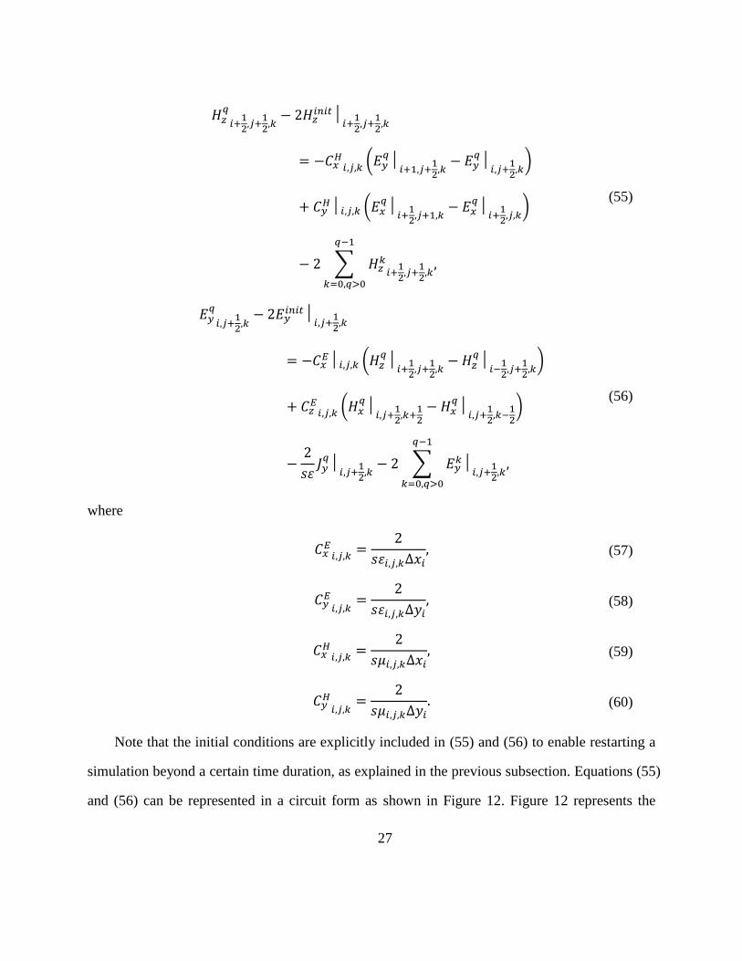
(
)
(
)
∑
(55)
(
)
(
)
∑
(56)
where
(57)
(58)
(59)
(60)
Note that the initial conditions are explicitly included in (55) and (56) to enable restarting a
simulation beyond a certain time duration, as explained in the previous subsection. Equations (55)
and (56) can be represented in a circuit form as shown in Figure 12. Figure 12 represents the
28
circuit model for the magnetic field
and the electric field
at the location
marked by the solid edges and their intersection in Figure 11. Only the partial 3-D model is
shown in Figure 12. The complete model can be derived in a similar fashion and is shown in
Appendix A.
Figure 12. Companion model of the 3-D FDTD grid in Laguerre domain.
The branch currents represent the qth Laguerre basis coefficient of the magnetic fields and
are given by
(61)
(62)
(63)
29
(64)
The nodal voltages represent the qth basis coefficient of the electric fields given by
(65)
In Figure 12, the branch-current circuitry represents (55) and the circuitry connected to the
node with voltage
represents (56).
The values of the current sources and the resistor in the branch-current circuitry in Figure 12
are
∑
(66)
(
) (67)
(68)
The current sources and the resister connected between the ground and the node with
voltage
in Figure 12 have the following values:
(69)
(70)
(71)
(72)
∑
(73)
The circuit given in Figure 12 can be stamped in a modified-nodal-analysis matrix [29] and
solved to find the unknown Laguerre basis coefficients of the electric and magnetic fields.
30
Solving the circuit shown in Figure 12 in the SLeEC method is equivalent to solving (46) in the
Laguerre-FDTD algorithm. In the Laguerre-FDTD algorithm, the recursive calculations of (46)
are needed as the order q increases. In the SLeEC method, the recursive calculations in the
Laguerre-FDTD approach are realized by obtaining DC solutions of the equivalent-circuit model
for each order q as the order q increases. The DC solution at the end of the qth iteration
represents the qth Laguerre basis coefficient of the electric and the magnetic fields. The DC
solution at the end of the qth iteration is used to update the companion model before solving for
the next set of Laguerre basis coefficients. The number of unknowns that needs to be solved in
the DC analysis can be reduced by using the Norton equivalent form [27] looking into the circuit
marked by the double arrow in Figure 12. The values of the Norton equivalent circuit are given
by
(74)
(75)
In (74), has terms involving and . Therefore, is a current-controlled current
source. In the modified nodal analysis [29], current-controlled current-source terms in
introduce additional unknowns, besides the unknown nodal voltages [30]. However, can be
implemented as a voltage-controlled current source and independent current source, by stamping
the current in a branch directly with the additional unknowns being eliminated. Voltage-
controlled current sources do not introduce additional unknowns [30]. The unknowns to be
solved are only the electric-field coefficients (nodal voltages). Therefore, the matrix dimension
to be solved is in its optimal form.
The partial model shown in Figure 12 can be extended in a similar fashion to satisfy the
complete set of Maxwell‟s differential equations in 3-D form in the Laguerre domain.
31
3.2.3 Choosing the Correct Number of Basis Functions
The final step of the Laguerre-FDTD is to convert the Laguerre-domain coefficients to time-
domain parameters at the output nodes of interest. Here, the number of basis functions used in
generating the time-domain waveform is very important to obtain accurate results because of the
time-domain waveform‟s sensitivity to the number of basis functions. A Fourier-transform-based
method to choose the number of basis functions in the Laguerre-FDTD is proposed in [24],
which is shown in detail in 3.2.3. However, the method only provides the minimum number of
basis functions and misses maximizing accuracy. The methodology for choosing the optimal
number of basis coefficients is improved in the SLeEC method to maximize the accuracy [32],
which is explained below.
1) Energy analysis (Step 1): Laguerre basis functions decay to 0 as time increases, as
shown in Figure 6, and decay slower as the order of Laguerre basis function increases.
Thus, for the later part of a time-domain waveform, which is computed as the sum of
weighted Laguerre basis functions, the number of basis function needs to be sufficiently
large. The minimum number of basis functions qknee to represent a time-domain
waveform can be found by analyzing the time-domain waveform‟s energy content as a
function of the number of basis functions.
Energy content E(q) is defined as a summation of the L1 norm:
( ) ∑ , -
(76)
where Wq is the time-domain waveform obtained using q+1 basis coefficients, and N is
the number of discrete time points making up the time-domain waveform.
The energy content as a function of the number of basis functions is shown in Figure 13.
When the number of basis function is larger than 100, those basis functions have
32
constant energy content. Therefore, qknee = 100 is considered as the minimum number of
basis functions to have sufficient energy to represent the time-domain waveform for the
time duration of interest.
Figure 13. Energy content as a function of the number of basis functions.
2) Finding the optimal number of basis functions (Step 2): Given the minimum
number of basis functions from Step 1, the correct number of basis functions which
maximizes the accuracy can be chosen by doing an error analysis. Using more Laguerre
basis functions does not always improve accuracy, which is explained in detail in
CHAPTER IV. Since the Laguerre basis function‟s value equals 1 at time t = 0
regardless of the basis function‟s order, minimizing the error at time t = 0 is sufficient to
determine the exact number of basis coefficients. The optimal number of basis functions
qopt is chosen between qknee,…, qmax in order to produce the smallest error at time t = 0.
By using a source waveform with initial value zero, the field values at all locations also
33
have the value zero at time t = 0. By starting the simulation in a known state, the initial
value is therefore known and can be used to minimize error at time t = 0.
Although this methodology for transformation from Laguerre domain to time domain
provides guidance in determining the number of basis functions, it still has limitations such as
spurious oscillations similar to Gibb‟s phenomena in the Fourier series. The methodology for
obtaining the time-domain waveform has been improved in this dissertation as compared to prior
work [32]. The efficient recovery of the time-domain waveform using a reduced number of basis
coefficients with an increased accuracy level is in detail in CHAPTER IV.
3.2.4 Node-Numbering Scheme
The SLeEC method requires solving a matrix of the form Ax=b at every iteration. However,
LU decomposition has to be done only once because the matrix stays constant throughout the
iterations. The matrix is sparse and symmetric. To make the matrix banded, the nodes are
numbered on a cell by cell basis.
Let us assume that the problem domain consists of nx × ny × nz cells where the label for the
ith Yee cell in the jth row on kth plane can be written as cell (ijk), as shown in Figure 14.
The nodes within a cell (000) at the corner are numbered first, and the nodes within an
adjacent cell in x direction, cell (100), are labeled next. In the case of the shared nodes between
cell (000) and cell (100), since all nodes within cell (000) are numbered prior to the numbering
of the nodes within cell (100), the shared nodes are skipped in the numbering of the nodes within
cell (100). Next, the nodes within the cell (200) are numbered in a similar fashion, and the
numbering scheme continues until it reaches cell (nx00). This numbering process is repeated for
the nodes within cells on other rows and planes, leading to the numbering of all the nodes that
define the structure.
34
Because of the local behavior of Maxwell‟s equations in a Yee cell, this form of node
numbering can lead to the A matrix being banded, as shown in Figure 15.
Figure 14. Efficient node-numbering scheme.
35
Figure 15. Sparsity pattern of the A matrix suitable for LU decomposition.
3.3 Advantages of using Laguerre Polynomials
Orthogonal polynomials are classes of polynomials pn(x) defined over a range [a, b] that
obey an orthogonality relationship in the form
∫ ( ) ( ) ( )
(77)
where w(x) is a weighting function and δmn is the Kronecker delta. A table of some orthogonal
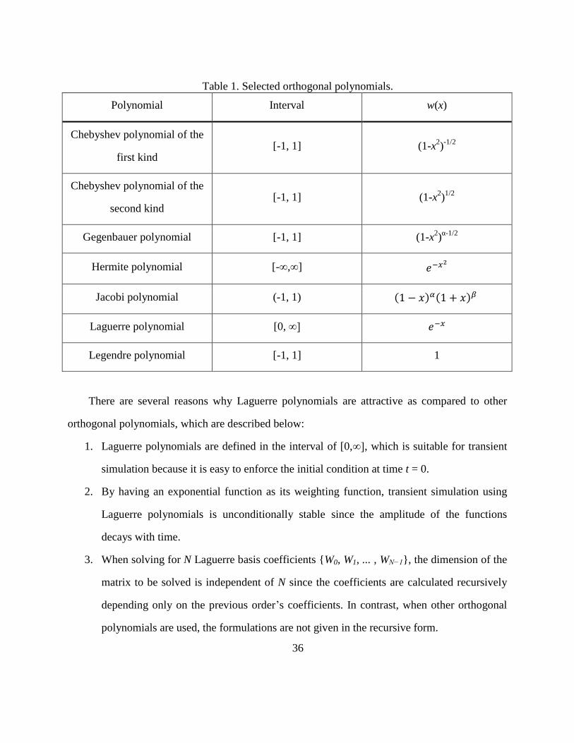
polynomials is given in Table 1, where w(x) is the weighting function.
36
Table 1. Selected orthogonal polynomials.
Polynomial Interval w(x)
Chebyshev polynomial of the
first kind [-1, 1] (1-x
2)-1/2
Chebyshev polynomial of the
second kind [-1, 1] (1-x
2)1/2
Gegenbauer polynomial [-1, 1] (1-x2)α-1/2
Hermite polynomial [-∞,∞]
Jacobi polynomial (-1, 1) ( ) ( )
Laguerre polynomial [0, ∞]
Legendre polynomial [-1, 1] 1
There are several reasons why Laguerre polynomials are attractive as compared to other
orthogonal polynomials, which are described below:
1. Laguerre polynomials are defined in the interval of [0,∞], which is suitable for transient
simulation because it is easy to enforce the initial condition at time t = 0.
2. By having an exponential function as its weighting function, transient simulation using
Laguerre polynomials is unconditionally stable since the amplitude of the functions
decays with time.
3. When solving for N Laguerre basis coefficients W0, W1, ... , WN−1, the dimension of the
matrix to be solved is independent of N since the coefficients are calculated recursively
depending only on the previous order‟s coefficients. In contrast, when other orthogonal
polynomials are used, the formulations are not given in the recursive form.
37
3.4 Summary
An unconditionally stable implicit-FDTD scheme using Laguerre polynomials has been
proposed, which is referred to as the Laguerre-FDTD scheme. Laguerre-FDTD can be
significantly faster than FDTD and other time-domain methods especially for packaging
problems containing multiscale dimensions. By using an implicit-solution technique, a decrease
in simulation time is possible at the expense of an increase in memory consumption. Most
importantly, because of Laguerre-FDTD‟s unconditional stability, the time-step limitation can be
removed. Since Laguerre-FDTD is a marching-on-in-time scheme, a time step larger than
Courant-Friedrich-Levy (CFL) limit does not deteriorate the accuracy of the simulation.
Since the introduction of the Laguerre-FDTD algorithm, several modifications have been
made to the algorithm for enhancing its performance. The modified algorithm has been named
SLeEC which stands for “Simulation using Laguerre Equivalent Circuit,” which uses an
equivalent-circuit model of the FDTD grid in the simulation. The SLeEC method enables the
transient simulation for a long time interval which has been difficult using the Laguerre-FDTD
scheme described earlier by other researchers. Also, the SLeEC method can be seamlessly
integrated into Spice simulators by using the equivalent-circuit models. In addition, the SLeEC
method provides the methodology for choosing the correct number of basis functions for
maximizing accuracy, and uses a node-numbering scheme that enables efficient LU
decomposition of the system matrix.
38
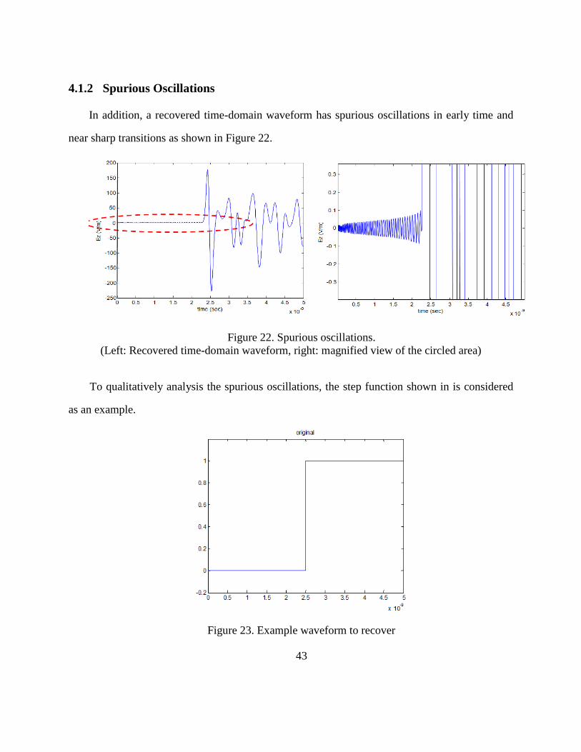
CHAPTER IV
GENERATING THE TIME-DOMAIN WAVEFORM FROM LIMITED
NUMBER OF LAGUERRE BASIS COEFFICIENTS
As stated earlier, in the Laguerre-FDTD method, a time-domain problem is rewritten and
solved in the Laguerre-domain. Since it is impossible to use an infinite number of Laguerre basis
functions in the calculation, an approximation with a finite number of Laguerre basis functions is
needed for accurate and efficient simulation.
4.1 Limitations of Prior Work
A Fourier-transform-based method to choose the number of basis functions in the Laguerre-
FDTD is proposed in [24], which is shown in detail in 3.2.3. However, the method only provides
the minimum number of basis functions and misses maximizing accuracy. To improve the
method to choose the number of basis functions, the SLeEC method proposed two steps to
choose the optimal number of basis functions [32], which is discussed in CHAPTER III in detail.
The first step is to calculate the energy contained in the time-domain waveform. The energy is
defined as a summation of the L1 norm. By analyzing the energy, the lower bound of the number
of basis functions can be found, which has enough energy to represent the time-domain
waveform for the desired time duration. The second step is to analyze error at the initial point (in
general, time t = 0) and choose the number of basis functions that gives the minimum error at the
initial point. The error at the initial point provides the statistical upper bound of error over the
whole simulated time duration as shown in Appendix B. However, the proposed method in [32]
does not guarantee the minimum error over the whole simulated time duration.
For example, for the given time-domain waveform shown in Figure 16, the energy analysis
(first step) shows that the number of basis function needs to be more than 100 as shown in Figure
39
17. Errors at time t = 0 are plotted with respect to the number of basis functions as shown in
Figure 18. Based on the error analysis, the SLeEC methodology picks 162, which generates the
smallest error at time t = 0, as the optimal number of basis functions, resulting in the recovered
time-domain waveform shown in Figure 19. Compared to the original time-domain waveform,
162 basis functions seem to produce an accurate waveform.
Figure 16. Example time-domain waveform to be recovered using Laguerree basis functions.
0 0.5 1 1.5 2 2.5 3 3.5 4 4.5 5-800
-600
-400
-200
0
200
400
600
800
1000
1200
Time (ns)
40
Figure 17. Energy content of the recovered waveform as a function of the number of basis
functions.
Figure 18. Error at t = 0 as a function of the number of basis functions.
0 20 40 60 80 100 120 140 160 180 2000
0.5
1
1.5
2
2.5
3
3.5
4x 10
4
q
Eq
100 110 120 130 140 150 160 170 180 190 20010
-1
100
101
102
103
X: 162
Y: 0.4652
q
Err
or
at
t=0
41
Figure 19. Recovered time-domain waveform using 162 basis functions compared with
original waveform.
4.1.1 One Optimal Number of Basis Functions for Multiple Time Points
However, good correlation between the recovered waveform using 162 basis functions and
the original waveform does not necessarily mean that 162 is the optimal number of basis
functions in terms of accuracy. A recovered waveform using 188 basis functions is considered
for comparison. At time t = 4.6 ns, the waveform using 162 shows better accuracy than one using
188 basis functions as shown in Figure 20. However, at time t = 4.35 ns, the use of 188 basis
functions produces a closer value to the original waveform than the use of 162 basis functions, as
shown in Figure 21, which means that the optimal number of basis function can be different at
each time point.
0 0.5 1 1.5 2 2.5 3 3.5 4 4.5 5-800
-600
-400
-200
0
200
400
600
800
1000
1200
Time (ns)
q=162
original waveform
42
Figure 20. Comparison of the recovered time-domain waveforms near t = 4.6 ns.
Figure 21. Comparison of the recovered time-domain waveforms near t = 4.35 ns.
4.54 4.56 4.58 4.6 4.62 4.64 4.66-770
-765
-760
-755
-750
-745
-740
-735
-730
-725
Time (ns)
q=188
q=162
Original waveform
4.325 4.33 4.335 4.34 4.345 4.35 4.355 4.36 4.365 4.37 4.375
970
975
980
985
990
995
1000
1005
1010
1015
1020
Time (ns)
q=188
q=162
Original waveform
43
4.1.2 Spurious Oscillations
In addition, a recovered time-domain waveform has spurious oscillations in early time and
near sharp transitions as shown in Figure 22.
Figure 22. Spurious oscillations.
(Left: Recovered time-domain waveform, right: magnified view of the circled area)
To qualitatively analysis the spurious oscillations, the step function shown in is considered
as an example.
Figure 23. Example waveform to recover
44
The waveform shown in Figure 23 is recovered using 50, 500, 5000, and 50000 basis
functions with the time scale factor s = 1e10, as shown in Figure 24, Figure 25, and Figure 26,
respectively.
Figure 24. Recovered waveform using 500 basis functions.
Figure 25. Recovered waveform using 5000 basis functions.
45
Figure 26. Recovered waveform using 50000 basis functions.
Figure 24, Figure 25, and Figure 26 show that the magnitude and frequency of spurious
oscillations decreases and increases respectively as the number of basis functions increases. Such
trend eliminates the probability that the spurious oscillations come from computational errors.
Also, the trend is the same as Gibbs effect in Fourier series. It is worthwhile to note that error
near the sharp transition point is not easily dampened just by increasing the number of basis
functions. Quantitative analysis of the spurious oscillations is left for future work.
4.2 New Method for Obtaining Accurate Transient Waveform
As the number of basis functions goes to infinity, the approximated solution with the finite
number of basis functions converges to its original solution. At a fixed time t = tfixed, during the
process of the time-domain solution converging to the original solution as the number of basis
function increases, the solution fluctuates near the original solution with decaying magnitude of
the fluctuation as shown in Figure 27. Therefore, the application of a low-pass filter to the
converging process enhances the accuracy of the solution by removing the fluctuations. Also,
46
compared to the unfiltered case, low-pass filtering provides faster convergence to the original
solution, resulting in a smaller number of basis functions to achieve the desired accuracy. The
following infinite-impulse-response (IIR) filter is chosen to wipe out the fluctuations:
( ) ∑ ( ) , (78)
( ) ( )
( ), (79)
( ) ( )
( ). (80)
where W is a raw waveform, W1 is the intermediate waveform in the filtering, W2 is the filtered
solution, and σ1 and σ2 are related to the strength of the filtering whose values are between 0 and
1. Both σ1 and σ2 are empirically chosen to be 0.95 in the example in this chapter. As shown in
Figure 28, the filtered solution converges more quickly and smoothly than the unfiltered solution
without fluctuations.
Figure 27. Converging trend. (Left: the time-domain solution, right: the time-domain
solution at time t=2.425ns as function of the number of basis functions)
Since the filtered solution converges more quickly to the solution than the unfiltered
solution, the number of basis functions required to ensure a certain level of accuracy can be
significantly reduced. As the simulation run time is directly proportional to the number of basis
47
functions in the Laguerre-FDTD, the use of fewer basis functions results in reduced simulation
time. On the other hand, by filtering the solution at each time point, error is minimized for the
overall simulated time duration. Therefore, spurious oscillations in early time disappear as shown
in Figure 29.
Figure 28. Convergence of the filtered solution.
48
Figure 29. Removal of spurious oscillations by filtering.
4.3 Numerical Results
A bird‟s-eye view of the modeled structure is shown in Figure 30 (a). The on-chip structures
along with the interface between the chip and the package are shown in Figure 30 (b). The
magnified view of the region marked by the circle in Figure 30 (b) is shown in Figure 30 (c). The
structure has on-chip interconnects in the metal layers M1 and M2, connected by vias and routed
on the redistribution layer, through the solder pads, to the package and routed as package-level
interconnects. The on-chip structures in Figure 30 (c) represent the interconnections in the M1
and M2 layers of an SRAM cell. A cross-sectional view of the structure is given in Figure 31.
One of the important features of the chip-package structure is the multiscale dimensions
from the nanometer (nm) range to the millimeter (mm) range, resulting in a scale ratio of
1:50,000 in this example. The on-chip structures that are in the nm scale require a very fine mesh,
and therefore the simulation time becomes prohibitively large using the conventional FDTD
scheme because of the CFL condition. The time-domain response of the electric field at the
49
location marked by „probe‟ in Figure 30 (a) up to 5 ns is computed. The modulated Gaussian
current source is used to excite the structure at the end of the package trace as shown in Figure
30 (a).
The structure has been simulated using the conventional FDTD, Laguerre-FDTD method
without filtering, and Laguerre-FDTD method with the proposed filtering method. The normal
SLeEC scheme without filtering requires 502 Laguerre basis functions while the Laguerre-FDTD
scheme with the proposed filtering process needs only 368 basis functions, which speeds up the
simulation by 33%, from 9 minutes to 6 minutes. The simulation results show very good
correlation between Laguerre-FDTD and FDTD as shown in Figure 32. Since the simulated
waveforms from Laguerre-FDTD with and without filtering are overlapped, they are
indistinguishable in the figure. Spurious oscillations in early time are suppressed by filtering as
shown in Figure 33. While it takes 30 hours using FDTD, the Laguerre-FDTD method with the
proposed filtering scheme in this chapter takes only 6 minutes to complete the simulation for the
same structure with the same number of cells. This represents a 300× speed up over the
conventional FDTD scheme. The simulations were run on a Pentium quad core, 2.4GHz
processor with 4GB RAM.
Figure 30. The bird‟s-eye view of a test chip-package structure.
50
Figure 31. Cross section of the test structure.
Figure 32. Simulated time-domain waveform using Laguerre-FDTD and FDTD.
51
Figure 33. Reduction of spurious oscillations in early time.
4.4 Summary
In the Laguerre-FDTD approach, a time-domain problem is converted into the Laguerre-
domain and solved in the Laguerre-domain. Since it is impossible to use an infinite number of
Laguerre basis functions in the calculation, a proper approximation with a finite number of
Laguerre basis functions is needed for the accuracy of the simulation. The SLeEC methodology
provides a method to find the optimal number of basis functions. However, the resulting time-
domain waveform is not globally optimal regarding the accuracy.
In this chapter, a method for maximizing the accuracy with the minimum number of basis
functions has been proposed, which reduces the simulation running time and increases the
accuracy of Laguerre-FDTD. The proposed method removes spurious oscillations in early time
as well. The proposed method has been verified through a chip-package co-simulation example.
The simulation result of the example shows that the transient simulation using the proposed
method is 300 times faster than FDTD while maintaining the accuracy.
52
CHAPTER V
SIMULATION FOR LONG TIME DURATION
Due to the behavior of Laguerre polynomials, the Laguerre-FDTD method has a limitation
on the maximum time duration over which the structure can be simulated [2]. Although the
SLeEC scheme proposed in [2] overcomes such limitation on the maximum time duration by
dividing total simulation time into different time intervals, it has a drawback that error is
accumulated as the number of time intervals increases. Hence, obtaining the low frequency
response using SLeEC is a challenge.
In this chapter, a method for simulating long time intervals using the Laguerre-FDTD
scheme is presented that can be used to compute the low frequency response in addition to the
high frequency response. The proposed method is applied to a multiscale structure example for
verification.
5.1 Difficulty in Calculation of Laguerre Basis Functions
The first five Laguerre basis functions are plotted in Figure 34. Since the Laguerre basis
function‟s fluctuation is too slow to describe the time-domain behavior of interest in the range of
nanoseconds or microseconds, time t is transformed into a scaled time using a time-scale factor
s and is used instead of t in the actual simulation:
(81)
However, in this section, the use of the time-scale factor is omitted for simplicity.
53
Figure 34. Weighted Laguerre polynomials for orders p = 0 to p = 4.
As shown in Figure 34, Laguerre basis function φp(t) decays to 0 as t increases where φp(t)
decays slower as its order p is higher. Therefore, as the time duration gets longer, higher order
Laguerre basis functions are required for accurate result in the approximation in (81). However,
it is difficult to compute Laguerre basis functions with higher order for a long time interval. The
Laguerre basis function is represented as the product of an exponentially decaying function and
the Laguerre polynomial. The nth Laguerre basis function φn(t) can be represented by
multiplying the Laugerre polynomial with an exponential function as:
( ) ( ) (82)
where Ln(t) stands for nth Laguerre polynomial.
Figure 35 (a) shows a flowchart of the approach used in [2] to compute φn(t). The Laguerre
polynomial of order p can be calculated by using the following recurrence relation:
( ) (83)
( ) (84)
0 5 10 15 20 25 30-0.5
0
0.5
1
Time (sec)
Magnitude
p=0
p=1
p=2
p=3
p=4
54
( ) ( ) ( ) ( ) ( ) (85)
By following the recurrence loop in Figure 35 (a), the Laguerre polynomial Ln(t) becomes
very large as the order n increases. Beyond a large enough order number, the basis functions
become too large to be represented using IEEE-754 floating-point standard, and therefore are
computed as Inf in the digital computer. On the other hand, as is well known, the exponential
function e-t/2
decays to zero rapidly and therefore the exponential function is treated as absolute
zero in the computer beyond a certain time point. Therefore, after some time, the basis function
no longer has any meaningful value and is represented as Inf×0 or NaN (not a number), as shown
in Figure 36. In Figure 36, the graph terminates abruptly around t = 1440 when the computer
cannot determine the value of the basis functions.
Therefore, because of the difficulty in computing Laguerre basis functions of high order for
long time interval, the Laguerre-FDTD method proposed in [24] has the limitation that
simulation can only be performed for a limited time duration and cannot be performed for all
time. The SLeEC scheme proposed in [27] overcomes such a limitation on the maximum time
duration by dividing total simulation time into different time intervals. However, it has a
drawback that error is accumulated as the number of time intervals increases. Hence, obtaining
the low frequency response using SLeEC is still a challenge. The ultimate solution for the
limitation on time duration is to enable the calculation of Laguerre basis functions with
sufficiently high order and long time durations.
55
(a) (b)
Figure 35. Algorithm to compute the Laguerre basis function.
(a): algorithm in the prior work, (b): proposed algorithm
Figure 36. Calculated 1000th Laguerre basis function by the prior method.
56
5.2 Introduction of Balanced Laguerre Polynomial and Balanced Exponential
Function
The previous limitation can be overcome by introducing a balancing process in the
recurrence loop as shown in Figure 35 (b). For the description of the balancing process in the
proposed algorithm, φn(t) is represented as follows:
( ) ( )
(86)
where
( ) ( )
(87)
(
) (88)
( ) and
( ) in (87) and (88) are called the balanced Laguerre polynomial and
balanced exponential function, respectively. Variable ( ) can be calculated using (83)-(85)
and (87). New parameters and variables such as θ, m, and k are introduced related to the
balancing process. θ is a threshold value that limits the magnitude of the balanced Laguerre
polynomial in the recurrence loop. Parameters m and k represent the strength of balancing
process and the degree of balancing, respectively. A relation between the balanced Laguerre
polynomials before and after the increment of degree of balancing is given by
( )
( ) (89)
where m should be selected to ensure
is large enough to handle in the IEEE-754 floating-
point standard. For large t,
can be too small to be represented as non-zero value in the
computer. It should be avoided since ( ) goes to zero by the increment in the degree of
balancing k in that case. Therefore, m needs to be sufficiently large to make
treatable in the
IEEE-754 floating-point standard.
57
A rule of thumb for representing m in terms of the threshold value is the following:
(90)
It is required to make the threshold value as follows in terms of m:
(91)
If (91) is satisfied, by (89), the magnitude of the balanced Laguerre polynomial becomes
approximately 1 as the degree of balancing increases.
The balancing process prevents the magnitude of balanced Laguerre polynomials from being
too large. If the magnitude of a balanced Laguerre polynomial gets larger than the threshold
value θ, the balancing process is performed by increasing the degree of balancing k. Since m and
t have positive values, the magnitude of the balanced Laguerre polynomial reduces as the degree
of balancing k increases, as shown in (89). Therefore, the balanced Laguerre polynomial will
always remain less than θ in the recurrence loop, which circumvents the NaN problem.
After the computation of ( ) is completed, the Laguerre basis function can be calculated
using (86). Hence, this formulation enables the application of the Laguerre-FDTD method for
computing the response over long time duration.
The computation of the 1000th Laguerre basis function φn(t) by the proposed method and
the prior method used in [27] is plotted in Figure 37. The method in [27] cannot calculate the
basis function φn(t) when t is larger than 1440, which is equivalent to 20 ns when the time-scale
factor is 7×10⁸. However, the proposed method successfully obtains the value of Laguerre basis
function at time t greater than 1440, as shown in Figure 37.
58
Figure 37. Calculated 1000th Laguerre basis function.
Red: proposed method, blue dots: prior method
5.3 Numerical Results
As shown in Figure 38, a coplanar transmission line in the package is connected to on-chip
coplanar line through solder bumps. Two ports are defined at each end of the package trace. The
structures are assumed to be lossless in this example. This structure has a scale ratio of 1:100,000,
which is from 200 nm of the on-chip via‟s diameter to 20 mm of the package interconnection‟s
length. Due to the very fine mesh required for the on-chip structure and the very small time step
based on the CFL condition, the estimated simulation time for 1 us long simulation is
approximately 212 days. This structure was simulated using Laguerre-FDTD with the proposed
method for calculating Laguerre basis functions, which took 36 hours. In this example, Laguerre-
FDTD showed 100× speed up over FDTD.
59
Figure 38. Coplanar transmission line structure from PKG to chip.
(a): top view (b): cross-sectional view
Since the transient response was computed for 1 us duration as shown in Figure 39, the
insertion loss (s21) from 1MHz to 10GHz could be extracted from the simulated time-domain
waveform using an FFT, as shown in Figure 40.
Figure 39. Simulated time-domain waveform at Port 1.
0 0.1 0.2 0.3 0.4 0.5 0.6 0.7 0.8 0.9 1
x 10-6
-1000
-800
-600
-400
-200
0
200
400
600
800
1000
time (sec)
Ez (
V/m
)
60
Figure 40. Insertion loss (s21) of the coplanar transmission line structure.
5.4 Summary
Due to the difficulty in calculating Laguerre basis functions for long time intervals,
Laguerre-FDTD has a limitation on the maximum time duration over which the structure can be
simulated. The SLeEC method uses a technique that enables simulation for long time intervals
by dividing, the total simulation time into different time intervals. However, it still has a
drawback that error accumulates as the number of time intervals increase. Hence, obtaining the
low frequency response using SLeEC has been a challenge.
This chapter has described a method to compute the transient response for long time
intervals using the Laguerre-FDTD method. To enable simulation from DC to high frequency,
the basis function representations have been modified in this chapter by introducing balanced
Laguerre polynomials and balanced exponential functions. A simulation result using the
proposed method has shown 100x speed up over the FDTD scheme, making it a viable candidate
for the co-simulation of chip-package interconnect structures.
61
CHAPTER VI
EFFICIENT FREQUENCY-DOMAIN ANALYSIS USING TIME-DOMAIN
SIMULATIONS
A methodology for obtaining frequency-domain parameters from time-domain simulations
is discussed in this chapter. If the time-domain response does not sufficiently decay to zero
before the end of the time duration of interest, due to spectral leakage, its discrete Fourier
transform has a series of lobes, which results in inaccurate frequency-domain parameters. To
avoid the special leakage problem, there are two solutions: run a time-domain simulation until
the transient response decays to zero, or apply a windowing function to the transient response
which forces the transient response to decay before the time duration ends. In this chapter, a
time-domain simulation technique to accelerate the damping which may reduce the simulation
run time is presented. Especially in low-frequency analysis, the time-domain simulation needs to
be performed for a long time. In the conventional FDTD method, since the size of the time step
is limited, simulation for long times requires a large number of iterations, resulting in an
increased run time. However, utilizing Laguerre-FDTD‟s marching-on-in-degree nature, a time-
domain simulation for low-frequency analysis can be performed without the consumption of
additional resources compared to mid or high frequency analysis. This is shown in this chapter,
followed by a numerical example.
6.1 Time-domain to Frequency-domain Transformation
Consider a two-port network as shown in Figure 41. A method introduced in this section for
the two-port network example can be easily extended to a multi-port network. For a two-port
network, Z11 and Z21 can be obtained from the following equations:
62
* ( )+
* ( )+ (92)
* ( )+
* ( )+ (93)
where F is the Fourier transform operator, Vi and Ii are the voltage and current at port i,
respectively. Z12 and Z22 can be calculated similarly.
Figure 41. Two-port network.
Voltage at a port is defined using the integral of electric field as follows:
∫
(94)
where C is an arbitrary path connecting both ends of the port.
Once Z parameters are calculated from the time-domain simulation, S parameters can be
calculated from the Z parameters using the following equations [33]:
( )( )
(95)
(96)
63
(97)
( )( )
(98)
where ( )( ) .
In a general multi-port network, the relation between S parameters and Z parameters is given by
, - (, - ) (, - ) (99)
where [S] and [Z] represents the S and Z parameter matrix, respectively, and In is the identity
matrix of size n.
6.2 Efficient Time-domain Simulation for Frequency-domain Analysis
As discussed in the previous section, frequency-domain analysis can be done using a time-
domain simulation. Since only a finite-length transient response can be performed, if the
transient response does not decay to zero within the simulated time duration, some energy leaks
out of the original spectrum into other frequencies, which is called “spectral leakage.” The
spectral leakage results in a series of lobes in the frequency domain and inaccurate frequency-
domain parameters. To avoid the special leakage problem, there are two solutions: run a time-
domain simulation until the transient response decays to zero, or apply a windowing function to
the transient response which forcefully makes the transient response decay before the time
duration ends. However, the second option which applies a windowing function may introduce
error in the calculation of frequency-domain parameters because it distorts the original transient
response. In this chapter, a time-domain simulation technique to accelerate the damping is
presented, which can reduce the required length of a time-domain simulation compared to the
first option to run a time-domain simulation until the transient response decays.
64
To make the transient response decay rapidly, use of a resistive source has been presented in
[34] [35] [36] [37]. However, none of these authors de-embedded the effect of the resistance at
the source location. In order to accelerate the decay of transient response for the frequency-
domain analysis of the two-port network shown in Figure 41, additional shunt resistors are
attached at each port as shown in Figure 42.
Figure 42. Two-port network with additional resistances at port locations.
When the resistances at the ports are sufficiently small, the resistors make the time-domain
waveform decay quickly after its excitation using the source current. In Figure 42, the network
with resistors outlined by dashed lines shows the modified network containing the original two-
port network. The relationship between the original network and the modified network can be
expressed as follows:
, - , -, (100)
, - , - , - , - (101)
, -, - , - (102)
where , - [ ] , , - [
] , , - [
] , , - [
] . Variables with an asterisk
represent respective variables in the modified network.
Inserting (100) and (101) into (102), we get:
65
, -(, - , - , -) , - (103)
(( , -, - ) , -), - , - (104)
Therefore, the Z parameters of the original network can be represented in terms of the modified
network‟s Z parameters as
, - ( , -, - ) , - (105)
Solving the modified network instead of the original network, the simulation run time can
be significantly reduced as the transient responses rapidly decay. By de-embedding the effect of
the additional resistances at ports in the modified network using (105), accurate frequency-
domain responses can be calculated using a time-domain simulation over a short time period.
This method can be extended to a multi-port network easily, if necessary.
6.3 Efficient Laguerre-FDTD Simulation for Low Frequency Analysis
Analysis of low frequency behavior using time-domain simulation requires the transient
response for a long time regardless of how quick the transient response reaches the steady state.
When the lower bound of the frequency range of interest is fL, the required length of the time-
domain simulation Tf is given by
(106)
In the FDTD method, the time step is restricted by the CFL limit as stated earlier. Therefore,
for low frequency analysis, numerous iterations are needed using the FDTD scheme, resulting in
a fairly long computation time. For example, if the required frequency range is halved, then the
time duration of the time-domain simulation should be doubled, which requires twice the
computation time.
However, in the Laguerre-FDTD‟s scheme, there is a time-scale factor and the time step is
not restricted. Because of the time-scale factor, as long as the percent bandwidth of the transient
66
response stays constant, computation time does not increase by adjusting the time-scale factor in
the case that the frequency range of interest is lowered.
For example, let us consider two cases for a given structure: (1) transient simulation for 5 ns
with a frequency range of interest from 500 MHz to 1 GHz, and (2) transient simulation for 5 us
with a frequency range of interest from 500 kHz to 1 MHz. If the FDTD method is used, Case (2)
requires 1000 times more computation time than Case (1) because the number of iterations is
1000 times larger. However, analysis of Case (2) using the Laguerre-FDTD method can be
performed with almost the same computation time required for Case (1) using the Laguerre-
FDTD by adjusting the time-scale factor and source‟s frequency in Case (2) by 1/1000 compared
to Case (1).
6.4 Numerical Results
The test structure is a 2.4 GHz band-pass filter structure shown in Figure 43. It is a 4-layer
structure in a homogeneous medium of relative dielectric constant 3.48. The filter dimensions are
3200 um × 3000 um × 16 um. The entire structure is enclosed in a PEC box and discretized into
72 × 68 × 15 = 73,440 cells. The conductor material is PEC. The dielectric material is assumed
to be lossless and non-dispersive. A modulated Gaussian source current is excited at each port in
the time-domain simulations. Since the structure is lossless and has a resonance near 2.4 GHz,
transient responses oscillate forever without damping, as shown in Figure 44. However, for the
case where resistors of 50 ohm are attached at all ports, the transient responses decay quickly as
shown in Figure 45. Figure 45 shows the electric field in the z direction at Port 1 after the
excitation of the source current at Port 1. Calculated S parameters are shown in Figure 46 and
compared with S parameters from a frequency-domain commercial tool Sonnet, which uses
method-of-moment analysis [38]. Comparison with the commercial tool shows good correlation
in this example.
67
Figure 43. 2.4GHz band-pass filter. (top: cross-sectional view, bottom: top view of the
layout of the M0 layer. Dots are separated by 50 um)
68
Figure 44. Oscillatory transient response.
Figure 45. Rapidly decaying transient response.
69
Figure 46. Calculated S parameters.
6.5 Summary
Frequency-domain analysis can be performed from time-domain simulations using an FFT.
For efficient time-domain simulations for frequency-domain analysis, a method that attaches
resistors at each port has been proposed, which dampens the transient responses. A relation
between the original network and the modified network with port resistors has been derived.
Therefore, the resistors can be de-embedded after the calculation of frequency-domain
parameters. For low-frequency results, being a marching-on-in-degree method, the Laguerre-
FDTD has an advantage in that the low-frequency response can be calculated efficiently without
consumption of considerable additional resources while the FDTD method suffers from large
numbers of iterations which consumes more run time.
70
CHAPTER VII
MODELING OF DISPERSIVE AND CONDUCTIVE MATERIAL IN 3-D
STRUCTURES
Luebbers introduced a frequency-dependent FDTD formulation for dispersive materials in
1990 [39]. In this chapter, a Laguerre-FDTD formulation to model wave propagation is
introduced using the Laguerre transform of the convolution operator. The proposed formulation
is verified with a numerical example and compared with the results from the FDTD formulation.
The comparison reveals that the frequency-dependent FDTD formulation for dispersive material
is properly implemented in the Laguerre domain so that frequency-dependent dispersive
materials can be analyzed using the Laguerre-FDTD simulation method.
7.1 Time-domain Formulation for Frequency-dependent Materials
In this section, materials are assumed to be linear and isotropic. The frequency-domain
information (such as permittivity and permeability) is Fourier transformed to a time-domain
susceptibility function [40]. For simplicity, only the permittivity (electric susceptibility) is
discussed in this section. The extension to magnetic permeability is similar. In the time domain,
we have
( ) ( ) ∫ ( ) ( )
(107)
where ( ), and represent the time-domain electric susceptibility function, permittivity of
free space, and infinite frequency relative permittivity, respectively.
71
7.2 Transformation of Convolution Operation from Time-domain to Laguerre-
domain
In order to represent (107) in the Laguerre domain, transformation of the convolution term
in (107) to the Laguerre domain is required. The Laguerre domain is based on orthonormal
Laguerre basis functions. As stated in the earlier sections, the ith Laguerre basis function φi(t) is
defined as the product of the ith Laguerre polynomial and an exponential function [24], given by
( ) ( ) (108)
where Li(t) is the ith Laguerre polynomial and s is the time-scaling constant.
Let X(t) and Y(t) be arbitrary time-domain waveforms defined for t > 0. They can be
represented in the Laguerre domain as a sum of Laguerre basis functions scaled by Laguerre
basis coefficients Xi and Yi, as shown in (109) and (110):
( ) ∑ ( )
(109)
( ) ∑ ( )
(110)
Their convolution Z(t) can be written as
( ) ( ) ( ) ∫ ( ) ( )
(111)
The Laguerre-domain representation of Z(t) can be written as
( ) ∑ ( )
(112)
Applying the temporal testing procedure with φi(t), Z(t)‟s ith Laguerre basis coefficients can be
obtained as follows:
72
∫ ( ) ( )
∫ ( )∫ ( ) ( )
(113)
Summation of Zi from i = 0 to n is given by
∑
∑∫ ( ) ( )
∫ ∑ ( )
∫ ( ) ( )
∫ ∑ ( )
∫ ( ) ( )
∫ (∑ ( ( )) ( ) ( )
∫ ( ) ( ) )
∑∫ ∫ ( ( ) ( ) ( )
( ))
(114)
where k=t-τ.
In (114), the following property of Laguerre polynomials has been used:
∑ ( )
∑ ( ) ( )
(115)
Since k and τ are independent variables, separating terms of k and terms of τ in (114), we get
∑
∑∫ ( ) ( ) ∫ ( )
( )
(116)
73
∑∫ ( ) ( )
∫ ( ) ( )
∑
From the summation of Zi in (116), the nth order Laguerre basis coefficient for the convolution
of X(t) and Y(t) is obtained as follows:
∑
∑
∑
∑
(117)
7.3 Laguerre-domain Formulation for Frequency-Dependent Materials
Under the assumption that ( ) is defined only for t > 0, (107) can be rewritten using the
infinite integral as
( ) ( ) ∫ ( ) ( )
(118)
This assumption is reasonable since the Laguerre transform is for functions of t defined for 0 ≤ t
≤ ∞. The Laguerre-domain representation of (118) can be written as
(∑
∑
)
( ) ∑ (
)
( ) ∑
(119)
where
74
∫ ( ) ( )
(120)
∫ ( ) ( )
(121)
∫ ( ) ( )
(122)
(123)
Maxwell‟s curl equations in differential form are
(124)
(125)
In (125), we assume that HB for linear and isotropic media.
By applying the curl operation to (125) and substituting (124), we get
( )
(126)
The first and second derivative with respect to time can be expressed as [24]
( )
∑*
∑
+ ( )
(127)
( )
∑*
∑ ( )
+ ( )
(128)
Now (126) is transformed into the Laguerre domain with consideration of the frequency-
dependent behavior of dispersive material using (127), and (128), which results in
75
*
∑ ( )
+
*
( ) ∑ ( )
+
(129)
Using (119), (129) can be rewritten as follows:
( )
*
∑
∑ ( ) ( )
∑ ∑( )
+
*
∑ ( )
+
(130)
The double curl on the left side in (130) can be represented in discretized form using Yee‟s space
lattice and the central difference scheme.
It is important to note that the right side of (130) consists of Laguerre basis coefficients up
to (n - 1)th order for E and Laguerre basis coefficients for the source current J, while the left side
has only nth order Laguerre basis coefficients for the electric field E. Therefore, (130) enables a
76
recursive calculation of Laguerre coefficients using previous coefficients for the electromagnetic
waves within structures containing dispersive material.
7.4 Customized Formulation for Dispersion Model
The frequency domain information is Fourier transformed to a time-domain susceptibility
function χ(t) [39]. A Laguerre-domain susceptibility function χi is calculated by transforming the
time-domain susceptibility function into the Laguerre domain. Using the Laguerre-domain
susceptibility function, the electric flux density can be represented in the Laguerre domain as
shown in the previous section:
(∑
∑
) (131)
where and represent the electric permittivity of free space, and the infinite frequency
relative permittivity, respectively.
Using (131), the frequency-dependent dispersion can be incorporated in the Laguerre-FDTD
simulations. However, due to the summation terms in (131), all previous solutions from order i =
0 to n - 1 are required to calculate , the nth order Laguerre basis coefficient for the electric
flux density. Therefore, as order increases in the Laguerre-FDTD computation steps, a
significant amount of memory is needed to store all solutions in the previous orders. Such a large
memory consumption for dispersion introduces inefficiency to the Laguerre-FDTD method in
solving practical problems containing dispersive materials.
7.4.1 Debye model
The Debye model satisfies the Kramers-Kronig relationship and results in an efficient model
for the frequency-dependent complex permittivity, given by
77
( ) ( )∑
(132)
where and represent the strength and time constants of various relaxation processes, is
the static permittivity, and is the permittivity at infinite frequency. To maintain an
approximately constant loss tangent over a bandwidth of a few decades, is required.
However, for simplicity, the case with is discussed in this section. It can be easily
extended to in a similar fashion. The frequency-domain susceptibility function is
( ) ( )
(133)
where and are the strength and time constant of the first-order Debye relaxation process. The
fourier transform of (133) is given by
( ) ( )
( ) (134)
where ( ) is the unit step function. The time-domain susceptibility function for the Debye
model is represented in the Laguerre domain as follows:
(135)
where
( )
(136)
and s is a time-scaling factor in the Laguerre-FDTD.
Equation (131) can be rewritten as follows:
(137)
where
∑
∑
(138)
Inserting (135) into (137), we have
78
(∑
∑
) (139)
By subtracting from , we get
(∑
∑
)
(∑
∑
)
(∑
∑
)
(∑
∑
)
( )
(140)
Using (140), can be calculated recursively as follows:
( ) for n>0, (141)
(142)
Therefore, using (137), (141), and (142), the Laguerre-FDTD formulation for the electric flux
density in the Debye media can be calculated recursively without storing all previous
solutions.
7.4.2 Lorentz model
The lorentz model is another commonly used mathematical model to account for the
dispersion. The Nth-order Lorentz dispersion model is given by
( ) ( )∑
(143)
79
where is the pole amplitude, is the pole location, and is the damping factor. For
simplicity, the case with is discussed in this section. The frequency-domain susceptibility
function for the Lorentz model is
( ) ( )
(144)
where is the pole amplitude, is the pole location, and is the damping factor. The
susceptibility in the time domain is obtained from (144) as follows:
( ) ( )
√
(√ ) ( ) (145)
Introducing complex numbers, (145) can be rewritten as
( ) (( )
√
( √
) ) ( ) (146)
where ( ) represents the imaginary part of a complex number.
Transforming (146) to the Laguerre domain, we have
( ) (147)
where
( )
√
( √ )
(148)
( √
)
( √ )
(149)
Equation (147) has the same form as (135) with different constants which are complex numbers.
Therefore, similar to the Debye model, the electric flux density in the Lorentz media also can
80
be calculated recursively as follows:
( ) (150)
where
( ) for n>0, (151)
(152)
7.5 Numerical Results
The proposed formulation is applied to an example containing a simple microstrip
transmission line, as shown in Figure 47. Two ports are defined at both ends of the microstrip
line whose length is 90 mm with conductor width and thickness of 3 mm and 10 um, respectively.
Dielectric thickness is 200 um. The substrate material is FR-4 and it is assumed to be dispersive
and modeled using a 1st order Debye model. Parameters for the Debye model are εs=4.301,
ε∞=4.096, and τ=2.294∙10-11
s [39].
Figure 47. Test structure: Microstrip transmission line.
Thin conductor thickness results in very long simulation time of 11 hours using FDTD
because of the small time step size of 33 fs, which comes from CFL limit determined by the
smallest mesh size of 1 mm × 1 mm × 10 us. However, Laguerre-FDTD could be used to solve
the same structure in 8 minutes on the same computer. In this example, Laguerre-FDTD showed
81
80× speed up over FDTD. The simulated time-domain waveforms of the electric field at the ports
show very good agreement between FDTD and Laguerre-FDTD, as shown in Figure 48.
Contrary to 1.3GB of memory consumption when the general Laguerre-FDTD formulation
for dispersion is used, the customized Debye formulation consumes 730MB as shown in Table 2.
Table 2. Memory consumption of general and customized formulation for Debye model.
Memory Consumption
General formulation 1.3GB
Customized formulation
for Debye model 730MB
To see the effect of material‟s dispersion on the transient response, the same structure has
been simulated without the frequency-dependent dispersive material property using a frequency-
independent permittivity of 4.301 with no loss. Figure 49 shows the time-domain waveform
variation as the material property changes from dispersive to non-dispersive.
82
Figure 48. Simulated time-domain waveforms.
Figure 49. Comparison between simulated time-domain waveforms with dispersive and non-
dispersive FR-4 model.
0 0.2 0.4 0.6 0.8 1 1.2 1.4 1.6 1.8 2
x 10-8
-2000
0
2000
4000
6000
8000
10000
12000
time(sec)
Ez(V
/m)
probe1 L-FDTD
probe2 L-FDTD
probe1 FDTD
probe2 FDTD
0 0.5 1 1.5 2 2.5 3 3.5 4 4.5 5
x 10-9
-2000
0
2000
4000
6000
8000
10000
12000
time(sec)
Ez(V
/m)
p1 nondispersive
p2 nondispersive
p1 dispersive
p2 dispersive
83
7.6 Summary
A Laguerre-FDTD formulation for frequency-dependent dispersive materials has been
presented and has been improved in terms of memory efficiency for Debye and Lorentz media.
Enabling recursive calculation of the electric flux density, the proposed formulation avoids
storing all previous solutions which leads to significantly reduced memory consumption. The
proposed formulation has been verified using a test example. Simulation results show that
Laguerre-FDTD with the proposed formulation solves the example structure with dispersive
material properties more efficiently than the general Laguerre-FDTD dispersion formulation in
terms of memory while maintaining the accuracy.
84
CHAPTER VIII
TEST CASES
To increase 3-D integration density, TSV interconnections are emerging as major
interconnection elements. Through fabrication in silicon substrate, TSV interconnections reduce
interconnection pitch compared to bonding wires. In addition, the direct vertical connection by
TSVs shortens electrical length, especially for communication between stacked chips. With these
features, the use of TSV interconnections can be extended to various integrated mixed-signal
system designs.
However, full-wave analysis of the TSV interconnections is challenging. The challenge
comes from thin oxide region around relatively thick and long conductor of the TSV. Due to the
CFL condition and thin oxide thickness, the time step in the conventional FDTD method needs to
be very small when a given structure contains TSV. Laguerre-FDTD has an advantage in the
simulation of such multiscale structures. Using the improvements of Laguerre-FDTD made in
this thesis, 3-D multiscale structures containing TSVs can be solved efficiently and accurately, as
shown in the following sections. In addition, non-multiscale structures have also been simulated
and correlated with measurement. All simulations in this chapter have been done on a 64-bit
machine with a 12 core Intel Xeon CPU and 48 GB RAM.
8.1 TSV Array
Usually, TSV interconnections are fabricated as an array in a silicon carrier and stacked
vertically to construct a system-in-package (SiP). Therefore, a TSV array is a basic structure in
3-D integrated systems and needs to be well-analyzed. In this section, a 3-by-3 TSV array is
analyzed in the frequency domain to compute S parameters using the Laguerre-FDTD method
and the problem has been extended to a 5-by-5 array to show scalability. Comparison of the
85
simulation results of the 3-by-3 TSV array with results from a commercial solver shows good
correlation, which confirms the accuracy of the Laguerre-FDTD.
8.1.1 3-by-3 TSV Array
The first test case is a 3-by-3 TSV array. A single-layered 3-by-3 TSV array is embedded
into a silicon substrate with dielectric constant and conductivity of 11.9 and 10 S/m, respectively.
TSV‟s copper diameter is 30 um with oxide thickness of 0.1 um. TSV‟s length is 100 um. TSVs
are separated from adjacent TSVs by 30 um in the array, as shown in Figure 50. The TSV array
structure is enclosed by a PEC boundary. 18 ports are defined between the ends of each TSV and
the closest PEC boundary, as shown in Figure 51. From TSV‟s oxide thickness of 0.1 um to
TSV‟s length of 100 um, the scale difference is 1:1000. The structure is discretized into 104 ×
104 × 15 = 162,240 cells as shown in Figure 51. The cell dimension varies from 0.1 um to 5 um
in the x and y directions. The cell dimension in the z direction is fixed at 20 um. TSV‟s circular
cross-section is discretized into 24 × 24 cells using a rectangular mesh, as shown in Figure 52. S
parameters are calculated from a set of time-domain simulations for 20 ns using the Laguerre-
FDTD method.
Figure 50. 3-by-3 TSV array. (left: top view, right: side cross-sectional view)
86
Figure 51. Ports definition on TSV array.
Figure 52. Discretization of circular cross section of TSV.
Some of the calculated S parameters using Laguerre-FDTD are plotted with S parameters
calculated using a commercial solver [41] in Figure 53. Excellent correlation is shown between
the Laguerre-FDTD and the commercial solver in Figure 53. For calculation of 18-port S
87
parameters, 18 time-domain simulations are required, with a separate source current excited at
each of the 18 ports. For each time-domain simulation, it takes 19 minutes to finish the
simulation using only one core of the multicore CPU and a memory consumption of 4.8 GB.
Therefore, total 18 × 19 = 342 minutes are required to perform frequency-domain analysis. On
the other hand, the commercial solver consumed 260 minutes and 3.5 GB of memory to calculate
the 18-port S parameters using four cores.
18 time-domain simulations using Laguerre-FDTD are independent of each other. Therefore,
they can be parallelized utilizing multicore CPU. If the Laguerre-FDTD simulations are
optimally parallelized, CPU time of 342 minutes using one core can be reduced to 85.5 minutes
using 4 cores.
Figure 53. Calculated S parameters of 3-by-3 TSV array.
8.1.2 5-by-5 TSV Array
The TSV array structure in the previous subsection is extended to a 5-by-5 TSV array as
shown in Figure 54. The top view and the cross-sectional view are similar to the previous
88
example‟s top and cross-sectional views shown in Figure 50. Dimensions of the structure are
similar to the previous 3-by-3 TSV array example. TSV‟s copper diameter and length are 30 um
and 100 um, respectively. Oxide thickness of the TSV is 0.1 um. Distance between adjacent
TSVs is 30 um. The structure is enclosed by a PEC boundary. The structure is discretized into
164 × 164 × 15 = 403,440 cells as shown in Figure 54. The Circular TSV geometry is discretized
into 24 × 24 cells similar to the previous 3-by-3 TSV array example, as shown in Figure 52. 50
ports were defined at each end of the TSV, as shown in Figure 54.
Figure 54. 5-by-5 TSV array.
Figure 55 shows calculated S parameters. For the calculation of 50-port S parameters, 50
time-domain simulations are required to excite all 50 ports. It takes 90 minutes and 10.5 GB to
perform one time-domain simulation. Therefore, 50 × 90 = 4500 minutes are required to perform
all 50 time-domain simulations. However, using the symmetry of the structure, only 6 time-
89
domain simulations can represent 50 time-domain simulations, as shown in Figure 56. Time-
domain simulations with excited TSVs marked by the same number can be reduced to one
representative time-domain simulation. For example, from the structure‟s symmetry, S11_1 is
the same as S3_1, S3_5, S15_5, S11_21, S23_21, S23_25, and S15_25. Therefore, time-domain
simulations with a current source at Port 5, 21, and 25 can be derived from a time-domain
simulation with current source at Port 1 by re-ordering ports.
Figure 55. Calculated S parameters of 5-by-5 TSV array.
90
Figure 56. Categorization of TSVs in 5-by-5 TSV array using symmetry.
Unfortunately, the commercial solver [41] was not able to solve the 5-by-5 TSV array
example on the machine with 48 GB RAM because of insufficient memory. Therefore,
comparison of the calculated S parameters using Laguerre-FDTD with the commercial solver
was not possible.
8.2 TSV-TSV Coupling
TSV noise coupling is expected to be a major concern for 3D-IC system design. With TSV
coupled noise, the system noise reliability decreases, RF sensitivity decreases, and the bit error
rate (BER) of a high-speed signal increases. To protect sensitive active circuits from TSV
coupling noise, it is important to estimate the noise transfer function between the TSVs. In [42],
a test vehicle for TSV-TSV coupling has been fabricated and coupling between TSVs has been
measured in the time domain. In this section, the test vehicle for TSV-TSV coupling is analyzed
using the Laguerre-FDTD and compared with the measurement data in [42], which ensures the
accuracy of the Laguerre-FDTD method for this example.
91
Figure 57 illustrates the structure of the TSV-TSV coupling test vehicle. Conductor material
for TSV and RDL is copper whose conductivity is 5.69e7 S/m. Oxide thickness of the TSV is
0.52 um while the diameter of the TSV conductor is 33 um. The structure is enclosed by a PEC
boundary with 100 um margin between the structure and boundary in each direction in the
Laguerre-FDTD simulation. The structure is discretized into 94 × 94 × 19 = 167,884 cells as
shown in Figure 58. Similar to the TSV array cases, the circular TSV cross-section is discretized
into 24 × 24 cells, as shown in Figure 52.
Figure 57. TSV-TSV coupling test vehicle.
92
Figure 58. Meshing of test vehicle.
A rectangular clock signal, which switches between 0 and 1 V with a rising/falling time of
40 ps and source resistance of 50 Ω, is injected into Port 1. The measurements have been
performed with the source at Port 1 with clock frequency of 100 MHz and 10 GHz.
Laguerre-FDTD simulation of the structure took 24 minutes and 5.3 GB of RAM. S
parameters were calculated from the Laguerre-FDTD simulation. Since a voltage source with a
source impedance is not implemented in the Laguerre-FDTD code, transient responses could not
be directly calculated using the Laguerre-FDTD. Therefore, S parameters of the structure were
extracted using the Laguerre-FDTD. 4 ports are defined in the S parameter calculation between
each TSV‟s end and PEC boundary. Transient responses were calculated in ADS [43] using the
extracted 4-port S parameters, as shown in Figure 59 and Figure 60. Calculated transient
responses at Port 2 for clock‟s frequency of 100 MHz and 10 GHz are shown in Figure 61.
Compared to the measured data, results using Laguerre-FDTD show good correlation.
93
Figure 59. Calculated S parameters
Figure 60. Simulation setup in ADS.
94
Figure 61. Coupled noise at Port 2. (left: 100 MHz clock, right: 1 GHz clock)
8.3 Microstrip Line with Return Path Discontinuity
Microstrip lines are key components to transmit high speed signals in electronic systems.
Therefore, the propagation characteristics of the microstrip line structures need to be carefully
studied and investigated. For model-to-hardware correlation, microstrip line structures are
fabricated, measured, and compared with the Laguerre-FDTD simulation. Since dielectric
material is not ideal, accurate modeling of dielectric material‟s dispersion is essential to obtain
good correlation to measurements.
In this section, three microstrip line structures are simulated and compared with the
measurements. This structure‟s physical dimensions are not small enough for Laguerre-FDTD to
show the advantage in the simulation time over the conventional FDTD method. Therefore, the
main purpose of the test cases in this section is to show model-to-hardware correlation and prove
the accuracy of modeling using the Laguerre-FDTD method.
95
8.3.1 Simple Microstrip Line
Figure 62 and Figure 63 show the cross-sectional side view and top view of the test case,
respectively. The structure has 4 metal layers. The microstrip transmission line is located on the
top layer, while the second layer is a solid ground plane. The dielectric material is FR-4 whose
relative dielectric constant is 4.5 and loss tangent is 0.025. The conductor material is copper
whose conductivity is 5.69e7 S/m. GSG500 microprobes have been used in the measurement.
In the Laguerre-FDTD simulation, the structure is surrounded by a PEC boundary with a 5
mm margin between the structure and the boundary in each direction, and is discretized into 29 ×
79 × 23 = 52,693 cells, as shown in Figure 64. The smallest and the largest mesh sizes in lateral
direction are 0.17 mm and 1.5 mm, respectively. The scale difference is 1:3200 (from 30 um
conductor thickness to 95.5 mm transmission line length). Ports are defined at both ends of the
transmission line.
Figure 62. Side cross-sectional view of microstrip line test case.
96
Figure 63. Top view of microstrip line test case.
Figure 64. Meshing of structure. (top view)
Time-domain simulation for 20 ns was performed to calculate the frequency-domain S
parameters, which consumed 30 minutes CPU time and 1.2 GB of memory. The calculated
insertion loss is plotted in Figure 65 with measurements, showing good correlation between them.
Oscillations in the calculated insertion loss is due to interaction between the microstrip line
structure and PEC boundary, which can be resolved by providing wider margin between the
structure and PEC boundary.
97
Figure 65. Calculated and measured insertion losses of microstrip-line test case.
8.3.2 Microstrip Line over Slot
This structure is similar to the previous test case. However, the ground plane at the second
layer has a slot, as shown in Figure 66. The length and width of the slot are 30.5 mm and 4.81
mm, respectively. The structure is also enclosed by a PEC boundary with a 5 mm margin and
discretized into 38 × 135 × 23 = 117,990 cells. The top view of the mesh is shown in Figure 67.
The smallest and largest lateral mesh sizes are 0.17 mm and 2 mm, respectively. The scale
difference is the same as the previous test case 1:3200, which is from 30 um conductor thickness
to 95.5 mm transmission line length. For 20 ns simulation, 3.4 GB of memory and 70 minutes of
CPU time were required using the Laguerre-FDTD approach. The calculated insertion loss is
shown in Figure 68 and compared with the measured insertion loss. Reasonably good agreement
between the Laguerre-FDTD simulation and the measurement is observed.
98
Figure 66. Top view (top) and side cross-sectional view (bottom) of test case.
Figure 67. Meshing of structure. (top view)
99
Figure 68. Calculated and measured insertion losses of the microstrip-line-over-a-slot test
case.
8.3.3 Microstrip Line over Small Holes
This test case is also similar to the previous one. However, there are 10 small holes on the
ground plane instead of a large slot, as shown in Figure 69. The holes have the same size of 0.76
× 0.76 mm. The spacing between holes is 2.54 mm. In the Laguerre-FDTD simulation, the
structure is enclosed by a PEC boundary with a 5 mm margin, and is discretized into 37 × 127 ×
23 = 108,077 cells. The way the structure is discretized is shown in Figure 70. The smallest and
largest lateral mesh sizes are 0.15 mm and 2 mm, respectively. The scale difference is the same as
the previous test case 1:3200, which is from 30 um conductor thickness to 95.5 mm transmission
line length, 1:3200.
100
Figure 69. Top view (top) and side cross-sectional view (bottom) of test case.
Figure 70. Meshing of structure. (top view)
It takes 3.1 GB of memory and 60 minutes of CPU time to solve the structure for 20 ns
using the Laguerre-FDTD method. From the time-domain simulation, frequency-domain S
parameters can be calculated. The calculated insertion loss is shown in Figure 71. Both the
simulated and the measured insertion loss show similar trend. However, the correlation does
have discrepancy.
101
Figure 71. Calculated and measured insertion losses of microstrip-line-over-small-holes test
case.
8.3.4 Importance of Modeling Dispersion
In real world, most dielectric materials are dispersive. Therefore, accurate modeling of
dispersion is important to make model-to-hardware correlation. Test cases shown in this section
contain dispersive FR-4 material. The effect of inaccurate modeling of dielectric loss is
investigated using the test cases in this subsection.
The Debye model can represent frequency-dependent material effectively and is given by
( ) ( )∑
(153)
where and represent the strength and time constants of various relaxation processes, is
the static permittivity, and is the permittivity at infinite frequency. To obtain constant loss
tangent for wide range of frequency, the order of Debye model N needs to be sufficiently large.
The frequency range of interest in the test cases of this section is from 50 MHz to 10 GHz. FR-
102
4‟s loss tangent is given as 0.025 in these test cases. The Debye model with N = 1 cannot provide
constant loss tangent over the frequency range of interest, as shown in Figure 72.
Figure 72. 1st order Debye model for tan δ = 0.025 at 10GHz
Using a 4th
order Debye model (N = 4), almost constant loss tangent can be obtained for the
frequency range of interest as shown in Figure 73.
Figure 73. 4th
order Debye model for tan δ = 0.025 at 50MHz ~ 10GHz
0 1 2 3 4 5 6 7 8 9 10
x 109
0
0.005
0.01
0.015
0.02
0.025
Freq. (Hz)
Loss t
angent
0 1 2 3 4 5 6 7 8 9 10
x 109
0
0.005
0.01
0.015
0.02
0.025
0.03
Freq. (Hz)
Loss t
angent
103
Differences in calculated S parameters using a 1st order Debye model and a 4
th order Debye
model for microstrip line structures tested in this section are shown in Figure 74 - Figure 76. The
simple microstrip line shown in Figure 63 has no return path discontinuity, and the microstrip
line over small holes shown in Figure 69 does not have severe return path discontinuity.
Therefore, insertion loss is mainly determined by the material‟s loss. Consequently, an
inaccurate modeling of FR-4‟s dispersive property worsens the accuracy of the calculated
insertion loss for the test cases as shown in Figure 74 and Figure 76, where deviations between
measurement and calculated insertion loss using the 1st order Debye model are more than 1 dB.
Therefore, the effective modeling of dispersion is important for obtaining accuracy. In the case
of the microstrip line over a slot, as shown in Figure 75, the effect of inaccuracy in the loss
tangent modeling is not as obvious as other test cases with no and little return path discontinuity.
It is because the insertion loss of the structure is dominated by the geometry of the structure, due
to its return path discontinuity.
104
Figure 74. Insertion of loss of simple microstrip line using a 1st order Debye model and
a 4th
order Debye model.
Figure 75. Insertion of loss of microstrip line over a slot using a 1st order Debye model and
a 4th
order Debye model.
105
Figure 76. Insertion of loss of microstrip line over small holes using a 1st order Debye model
and a 4th
order Debye model.
8.4 Microstrip Line with TSV on Silicon Carrier
As stated in the previous section, a microstrip transmission line is a key component for
transmitting high-speed signals in electronic systems. As 3-D integration using TSV
interconnections emerges, microstrip lines with TSV interconnections on a silicon carrier also
need to be analyzed. Due to oxide‟s very thin thickness compared to TSV‟s diameter and length,
microstrip lines with TSVs are challenging structures to be analyzed using the conventional
FDTD method because of the CFL limit, whereas Laguerre-FDTD is advantageous in the
simulation of such multiscale structures.
8.4.1 Microstrip Line with Return Path Discontinuity I
Figure 77 shows a front cross-sectional view and a top view of the test case. The structure
contains 4 metal layers. A microstrip line starts on the top layer with TSV transitions to the
106
bottom layer and from the bottom layer to the top layer. The second and third layers are not
connected. Therefore, a return path discontinuity occurs at the TSV transition.
Figure 77. Front cross-sectional view and top view of test case.
The conductor material is copper whose conductivity is 5.69e7 S/m. Silicon‟s dielectric
constant and conductivity are 11.9 and 10 S/m, respectively. The TSV‟s copper diameter is 30
um and its oxide thickness is 0.1 um. The metal layer‟s thickness is 1 um. The dielectric layer‟s
thickness is 45 um which consists of 43 um of silicon and 1 um of oxide at the top and bottom of
the dielectric layer to insulate the conductive silicon layer from conductors. From 0.1 um of
TSV‟s oxide thickness to 430 um of transmission line‟s length on the top layer, the scale
difference is 1:4300 in this structure. The structure is discretized into 104 × 152 × 29 = 458,432
cells as shown in Figure 78. Due to TSV‟s circular geometry and thin oxide, the mesh for the
region occupied by TSV is very fine, as small as 0.1 um. The circular geometry of the TSV is
discretized into 24 × 24 cells as shown in Figure 79. Similar to the TSV array cases, the circular
cross-section of the TSV is discretized into 24 × 24 cells as shown in Figure 52. Two ports are
defined at both ends of the microstrip line. Transient simulation for 20 ns is performed to
calculate S parameters using the Laguerre-FDTD method, which takes 150 minutes and 23 GB
of RAM. If the structure was simulated using the conventional FDTD, because of CFL limit, the
107
time step needs to be as small as 0.16 fs, resulting in 268 days to solve the structure only for 20
ns. Memory consumption of FDTD is 38.4 MB. Therefore, Laguerre-FDTD shows 2500× faster
simulation than the conventional FDTD in this test case while the memory consumption of the
Laguerre-FDTD is 600× larger than FDTD.
Figure 78. Meshing of structure. (top view)
108
Figure 79. Discretization of circular cross section of TSV
Calculated insertion loss is shown in Figure 80. Unfortunately, the result cannot be
compared since both FDTD method and commercial tools cannot solve the structure due to time
and memory limitations, respectively.
Figure 80. Calculated return loss (left) and insertion loss (right).
109
8.4.2 Microstrip Line with Return Path Discontinuity II
This test case is introduced in [44] and shown in Figure 81. The test case in this subsection
is similar to the previous one in 8.4.1. The dimensions and composition of layers are different
from the test structure in 8.4.1. Two ports are defined at both ends of microstrip line between
microstrip line‟s conductor on the top layer and the solid plane on the second layer. The structure
is discretized into 94 × 263 × 31 = 766,382 cells. The lateral mesh is shown in Figure 82. As
shown, the mesh near the TSV structures is very dense. The smallest mesh size is 1 um, and the
largest mesh size is 800 um. The scale difference in this structure is from 1 um of TSV‟s oxide
thickness to 20 mm of bottom layer‟s conductor‟s length, 1:20000. Laguerre-FDTD simulation of
the structure takes 319 minutes and 44 GB of memory. If the structure were simulated using the
conventional FDTD method, the estimated CPU time is 22 days, which is 100× longer than the
Laguerre-FDTD. From the transient simulation using the Laguerre-FDTD method, S parameters
can be calculated. The insertion loss is plotted in Figure 83 and compared to the result in [44],
which is calculated using a commercial time-domain solver. Reasonably good agreement is
observed in the comparison.
Figure 81. Front cross-sectional view and top view of test case.
110
Figure 82. Meshing of structure.
(top: whole structure, bottom: enlarged view of red-circled area)
Figure 83. Calculated insertion loss.
111
8.4.3 Microstrip Line with TSV transition and no Return Current Discontinuity
Figure 84 illustrates the test case in this subsection. The structure consists of 4 metal layers.
A microstrip line runs on the top and bottom layers with a TSV transition. The second and third
layers are connected by 8 TSVs near the signal TSV from the top layer to the bottom layer. The
materials and layer composition are the same as the test case in 8.4.1. Two ports are defined at
ends of the transmission line. The structure is surrounded by a 500 um air margin and a PEC
boundary.
Figure 84. Expanded bird‟s-eye view and front cross-sectional view of test case.
After discretizing the structure into 152 × 152 × 29 = 670,016 cells, Laguerre-FDTD
simulation was performed. The lateral mesh between the second and third layers near the TSVs
is shown in Figure 85. The very fine mesh for capturing the thin oxide of the TSV is too fine to
112
be distinguished in the figure. The smallest and largest sizes of the lateral mesh are 0.1 um and
0.1 mm, respectively. The scale difference in the physical dimensions is from 0.1 um of the
TSV‟s oxide thickness to the 490 um of the microstrip line‟s length, 1:4900. Laguerre-FDTD
takes 40 GB of memory and 280 minutes of CPU time to solve the structure in the time domain
for 20 ns. However, the thin thickness of the TSV‟s oxide compared to the microstrip line‟s
lateral dimension results in a very long simulation time of 400 days using FDTD because of the
small CFL time step size of 0.16 fs. In this example, Laguerre-FDTD shows 2000× speed up
over FDTD while consuming 720× more memory. The calculated insertion loss is plotted in
Figure 86. Similar to the previous test case, the result could not be compared because both FDTD
method and commercial tools have difficulty in solving the structure.
Figure 85. Lateral mesh near TSVs between second and third metal layer.
113
Figure 86. Calculated return loss (left) and insertion loss (right).
8.5 Complexity Scaling
Complexity analysis for the Laguerre-FDTD method has been studied. The memory
complexity of the process is O(N4/3
), where N is the number of unknowns. The computational
complexity of the process is also O(N4/3
). PARDISO solver in Intel‟s math kernel library [45] has
been used to solve matrix equations resulted from the Laguerre-FDTD method. Results of the
complexity analysis has been done on a 32-bit machine with 2 GB RAM with an Intel Core 2
Duo E4500 processor are shown in Figure 87.
114
Figure 87. The scaling of memory complexity (left) and computational complexity (right).
8.6 Summary
In this chapter, the Laguerre-FDTD introduced and improved in this thesis has been applied
to various practical examples. Successful model-to-hardware correlation has been shown as well
as correlation with a commercial solver [41].
In the TSV array test cases, Laguerre-FDTD has shown excellent correlation to the
commercial solver. The computation time is also competitive compared to the commercial
solver‟s computation time. Excellent agreement has been shown in the TSV-TSV coupling
example between the Laguerre-FDTD simulation and the time-domain measurement. It affirms
the accuracy and the validity of the modeling of multiscale structures using Laguerre-FDTD.
Additional model-to-hardware correlations also have been made in the microstrip line examples
in 8.3. Three microstrip line test cases show good correlations to the measured S parameters.
Through examples containing both microstrip lines and TSVs in Section 8.4, Laguerre-FDTD‟s
scalability and advantage in the simulation of multiscale structure have been shown. Over 2000×
115
speed up is possible by using the Laguerre-FDTD method compared to conventional FDTD.
Examples shown in this chapter are summarized in Table 3. Finally, the scaling of complexity
has been performed. Both the memory complexity and the computational complexity of the
Laguerre-FDTD are O(N4/3
) when PARDISO solver is used.
Table 3. Summary of test cases
Test case # of
cells
CPU time
(mins)
Memory
(GB) Remark
3-by-3 TSV array 162k 342 4.8 Correlation with
commercial tool
5-by-5 TSV array 403k 4500 10.5 Commercial tool was
unable to solve
TSV-TSV coupling 168k 24 5.3 Correlation with
measurement
Simple ML 53k 30 1.2 Correlation with
measurement
ML over a slot 118k 70 3.4 Correlation with
measurement
ML over small holes 108k 60 3.1 Correlation with
measurement
ML on Si carrier with RPD I 458k 150 23 2500× speed up
compared to FDTD
ML on Si carrier with RPD II 766k 319 44
100× speed up
compared to FDTD,
Correlation with
commercial tool
ML on Si carrier with no RPD 670k 280 40 2000× speed up
compared to FDTD
116
CHAPTER IX
CONCLUSION
The need for high performance, small size, and low cost solutions for functional integration
is becoming more significant for the semiconductor industry. To satisfy this need, 3-D
integration is an unavoidable option to increase the required integration density. As more
functionality is integrated in the package, the electromagnetic interactions within the package
pose a significant problem. It requires a tool for design and analysis of ICs and the package
structures together at the same time, which is also called chip-package co-simulation and co-
design.
In the chip-package co-simulation and analysis of 3-D interconnection structures, large scale
differences in physical dimensions of the structure should be dealt with. EM simulation of such
multiscale structures using conventional FDTD is challenging because of CFL condition that
limits the time step. Laguerre-FDTD and SLeEC methodologies have been proposed to
overcome the limitation on the time step. However, they still have limitations for practical 3-D
integration problems, e.g., difficulty to obtain the low-frequency response and to treat lossy
materials. This provides motivation for research on the improvement of the Laguerre-FDTD to
make it applicable for practical problems arising in 3-D integration. The following section
clarifies the major contributions in this dissertation, emphasizing the usefulness of the proposed
method for the electrical design of 3-D integrated systems.
9.1 Contribution
9.1.1 Generating time-domain waveforms from solutions in Laguerre domain
A method to efficiently convert solutions from the Laguerre domain into the time domain
has been proposed. Applying a filter in the construction of the transient waveform from the
117
solutions in the Laguerre domain, a smaller number of Laguerre basis functions can be used in
the simulation while maintaining or even enhancing the accuracy compared to the conversion
scheme in the prior work [46].
9.1.2 Simulation for Long Time Intervals
The limited time duration for which the Laguerre-FDTD could be simulated has been
resolved by the introduction of the balanced Laguerre basis function and the balanced
exponential function. The Laguerre-FDTD method can now be executed for any length of time,
enabling the computation of the low frequency response.
9.1.3 Frequency-domain Analysis Method using Laguerre-FDTD
An efficient time-domain simulation methodology for frequency-domain analysis has been
proposed. By attaching shunt resistors at ports, the time-domain response decays quickly so that
time-domain simulation can be completed in a short time duration. The effect of the additional
resistances is de-embedded after the calculation of frequency-domain parameters. An efficient
low-frequency analysis methodology using the Laguerre-FDTD approach also has been
presented. By adjusting the time-scale factor in the Laguerre-FDTD, long-time transient
simulations can be performed with no additional effort compared to short-time transient
simulation for high-frequency analysis.
9.1.4 Modeling of Dispersive and Conductive Materials
A Laguerre-FDTD formulation for frequency-dependent dispersive materials has been
proposed. Inclusion of dispersive materials in the simulation is critical to solving practical
problems. For Debye and Lorentz media, the proposed formulation has been improved by
enabling a recursive calculation of the electric flux density, which results in a significant
reduction of the memory consumption.
118
9.2 Publications ( from This Work)
Myunghyun Ha, and Madhavan Swaminathan, “Memory-Efficient Laguerre-FDTD
Formulation for Debye and Lorentz Media,” submitted to IEEE Microwave and Wireless
Components Letters.
Myunghyun Ha, and Madhavan Swaminathan, “Minimizing the Number of Basis
Functions in Chip-Package Co-Simulation Using Laguerre-FDTD,” IEEE International
Symposium on Electromagnetic Compatibility, Pages: 905-909, Long Beach, CA, Aug.
2011.
Myunghyun Ha, and Madhavan Swaminathan, “A Laguerre-FDTD Formulation for
Frequency-Dependent Dispersive Materials,” IEEE Microwave and Wireless
Components Letters, Page(s):225-227, Volume 21, Issue 5, May 2011.
Myunghyun Ha, Joong-Ho Kim, Dan Oh, and Madhavan Swaminathan, “A Study of
Reduced-terminal Models for System-level SSO Noise Analysis,” IEEE 19th Conference
on Electrical Performance of Electronic Packaging, Pages: 49-52, Austin, TX, Oct.
2010.
Myunghyun Ha, Krishna Srinivasan, and Madhavan Swaminathan, “Transient Chip-
Package Co-simulation Using the Laguerre-FDTD Scheme,” IEEE Transactions on
Advanced Packaging, Page(s):816-830, Volume 32, Issue 4, Nov. 2009.
Krishna Srinivasan, Pradeep Yadav, Ege Engin, Madhavan Swaminathan, and
Myunghyun Ha, “Fast EM/Circuit Transient Simulation Using Laguerre Equivalent
Circuit (SLeEC),” IEEE Transactions on Electromagnetic Compatibility, Page(s):756-
762, Volume 51, Issue 3, Part 2, Aug. 2009.
119
Myunghyun Ha, Krishna Srinivasan, and Madhavan Swaminathan, “Chip-Package Co-
Simulation with Multiscale Structures,” IEEE 17th Conference on Electrical
Performance of Electronic Packaging, Page: 339-342, San Jose, CA, Oct. 2008.
9.3 Publications ( from Past Work)
Jiwoo Pak, Myunghyun Ha, Jaemin Kim, Donghee Kang, Ho Choi, Seyoung Kwon,
Keunsoo La, and Joungho Kim, “Design of a 3-D SiP for T-DMB with Improvement of
Sensitivity and Noise Isolation,” IEEE Electronics Packaging Technology Conference,
Page(s) 1387-1392, 2008.
Gawon Kim, Dong Gun Kam, Seung Jae Lee, Jaemin Kim, Myunghyun Ha,
Kyoungchoul Koo, Jun So Pak, and Joungho Kim, “Modeling of Eye-Diagram
Distortion and Data-Dependent Jitter in Meander Delay Lines on High-Speed Printed
Circuit Boards (PCBs) Based on a Time-Domain Even-Mode and Odd-Mode Analysis,”
IEEE Transactions on Microwave Theory and Techniques, Page(s) 1962-1972, Volume
56 , Issue 8, 2008.
120
CHAPTER X
FUTURE WORK
The current contributions of this dissertation can be improved in their applicability to
analysis of practical 3-D integrated systems by completing the following future work. The future
work is specified for modeling of nonlinear phenomena and modeling of skin effect.
10.1 Modeling of Nonlinear Phenomena
In 3-D-integrated systems, the semiconductor‟s nonlinear property plays an important role.
For example, the TSV‟s effective capacitance depends on bias voltage between the TSV and the
silicon substrate. Such characteristics cannot be described with linear equations. In addition,
modeling of a channel in a system requires the accurate model of receivers and transmitters
which are connected at the end of the channel. Those receivers and transmitters consist of
nonlinear devices such as transistors. Therefore, to describe such nonlinear properties, inclusion
of nonlinear phenomena in the interconnection modeling is required.
However, it is not easy to incorporate nonlinear phenomena in the Laguerre-FDTD method
since the Laguerre transform of a nonlinear operation is very difficult. Therefore, proper and
clever approximations are needed to model the nonlinear phenomena in the Laguerre-FDTD
method.
10.2 Modeling of Skin Effect
Conductor losses result in skin effect. Conductivity is already taken into account in the
current Laguerre-FDTD formulation. However, to capture the skin effect accurately, very fine
meshes near the surfaces of conductors are required because the electric field inside the
conductor exponentially decreases as fields penetrate into the conductor from its surface, which
increases the number of unknowns. If a proper skin effect model can be derived for the Laguerre-
121
FDTD method, the skin effect can be incorporated without using a fine mesh near the conductor
surface.
Due to the skin effect, the effective thickness of conductors varies with frequency, which
results in the change of effective resistance of a conductor with respect to frequency. In
CHAPTER VII, it has been shown how to formulate a material‟s frequency-dependent dielectric
constant in Laguerre-FDTD. Similarly, a frequency-dependent resistivity can be formulated in
Laguerre-FDTD.
122
APPENDIX A: DERIVATION OF COMPLETE 3-D MODEL OF SLEEC
Consider the following six Maxwell‟s differential equations [12]:
(
) (154)
(
) (155)
(
) (156)
(
) (157)
(
) (158)
(
) (159)
Consider the standard FDTD Yee cell [11] shown in Figure 88. The cross sections of the
FDTD cell at the locations marked by the dotted lines in Figure 88 are shown in Figure 89. The
cross sections in Figure 8 are viewed by standing on the +∞ of y, x, and z axis and facing the Yee
cell, respectively.
123
Figure 88. Standard Yee cell.
Figure 89. Sections of the Yee cell marked by the dotted lines in Figure 7 parallel to the xz,
yz, and xy planes, respectively. Dots indicate direction of the fields pointing out of the page.
Converting (154)-(159) into the Laguerre-domain and rewriting them in a matrix form in
after discretization using the central-difference scheme in space as shown in Figure 88 and
Figure 89, we have
124
(
)
(
)
∑
(160)
(
)
(
)
∑
(161)
(
)
(
)
∑
(162)
125
(
)
(
)
∑
(163)
(
)
(
)
∑
(164)
(
)
(
)
∑
(165)
where
(166)
(167)
(168)
(169)
126
(170)
(171)
Replacing the electric and magnetic fields in equation (160)-(165) with the nodal voltages
and the branch currents, we have
(
)
(
)
∑
(172)
(
)
(
)
∑
(173)
127
(
)
(
)
∑
(174)
(
)
(
)
∑
(175)
(
)
(
)
∑
(176)
(
)
(
)
∑
(177)
Equation (172)-(177) can be represented in a circuit form using controlled sources as
follows:
128
(178)
(179)
(180)
(
)
(181)
(
)
(182)
(
)
(183)
where
(184)
129
(185)
(186)
(187)
∑
(188)
(189)
(190)
(191)
(192)
∑
(193)
(194)
(195)
(196)
(197)
∑
(198)
(199)
130
(
) (200)
∑
(201)
(202)
(
) (203)
∑
(204)
(205)
(
) (206)
∑
(207)
Schematic of the companion model described in (178)-(207) in the 3-D FDTD grid is
shown in Figure 90 with the associated electric fields in the 3-D FDTD grid shown in Figure 91.
131
Figure 90. Companion model of the 3-D FDTD grid in Laguerre domain.
Figure 91. Electric fields in the 3-D FDTD grid.
132
The circuit given in Figure 90 can be stamped in a modified-nodal-analysis matrix [29] and
solved to find the unknown Laguerre basis coefficients of the electric and magnetic fields.
133
APPENDIX B: MATHEMATICAL JUSTIFICATION FOR ERROR
ANALYSIS AT THE INITIAL POINT
Let ( ) be the original solution of the time-domain waveform which is represented as a
sum of infinite number of weighted Laguerre basis functions where Ep represents pth Laguerre
coefficient corresponding to the pth Laguerre basis function ( ):
( ) ∑ ( )
(208)
where , s is a time-scale factor. Using an approximation with N basis functions, the
waveform is now represented as
( ) ∑ ( )
(209)
The error ( ) at time t can be written as
( ) ( ) ( )
∑ ( )
∑ ( )
∑ ( )
∑ ( )
(210)
Since ( ) is approximated using the first N basis functions, EN, EN+1, EN+2, … are unknown
while E0, E1, …, EN-1 are known. Let us assume Ep where be a random variable with
normal distribution (mean and variance ) given by
( ) for . (211)
134
Error at time t = 0 can be calculated as
( ) ( ) ( )
∑ ( )
∑ ( )
∑ ( )
(212)
The mean of Ep is given by
( ) ∑ ( )
(213)
Therefore, under the assumption that Ep for is a Gaussian random variable, its mean
should be zero.
Since the sum of M Gaussian random variables with zero mean and variance is another
Gaussian random variable with zero-mean and variance , error at t = 0 is a Gaussian random
variable with zero-mean and variance while M goes to infinity:
( ) (
∑
) (214)
Similarly, error at t > 0 also can be represented as a Gaussian random variable since it is the
sum of weighted Gaussian random variables. While its mean is still zero, Since ( ) for t >
0, as shown in Figure 92, variance of error ( ) is always smaller than variance ( ) of for t > 0:
135
( ( ))
∑ ( )
∑
( ( ))
(215)
Figure 92. Laguerre basis functions for orders p = 0 to p = 4.
Since ( ) is smaller than 1 for t > 0, as shown in Figure 92, ( ( )) is smaller than
( ( )) . Their probability density functions can therefore be approximated as shown in
Figure 93. The probability that ( ) is greater than ( ) for t > 0 is very small, which implies
that ( ) ( ) for t > 0 in most cases. Therefore, in most cases, error at time t > 0 is
bounded by error at time t = 0. Thus, minimizing error at time is effective in reducing error at t >
0.
0 5 10 15 20 25 30-0.5
0
0.5
1
Time (sec)
Magnitude
p=0
p=1
p=2
p=3
p=4
136
Figure 93. Probability density functions of normal distribution with large and small
variances.
137
APPENDIX C: SLEEC SOFTWARE
I. Overview.
SLeEC is a transient EM solver for multiscale structures. SLeEC consists of files shown in
Table 4.
Table 4. Configuration of SLeEC software.
File name Remarks
SLeEC.exe SLeEC engine executable file
Config.txt SLeEC Configuration file
As shown in Figure 94, SLeEC reads two input files in ASCII format which can be easily
modified using text editors such as notepad: structure description file (*.sd) and simulation setup
file (*.ss). Simulation description file has information about the structure. No information related
to simulation is contained. Simulation setup file has information about setup of simulation such
as port and source definitions. Both files are explained in detail in the later part of this appendix.
138
Figure 94. Flow chart of SLeEC software.
SLeEC performs time domain analysis. If user wants to do the time domain analysis,
simulation setup file has information about simulation setup such as simulation time, source
waveform, and probing point.
Following output files are generated by simulation: time domain waveform (*.txt) and
Laguerre coefficients for simulated time domain waveform (*.txt). Time domain waveform file
have series of numbers that represents time line in second, source current in Ampere, probed
electric field value in V/m. Laguerre coefficient output file contains Laguerre coefficients of
simulated time domain waveforms. Normally, this output file can be ignored since Laguerre
coefficient itself does not have much value from user‟s point of view. Time domain waveform
built from the Laguerre coefficients are contained in the time domain waveform output file.
II. Execution of SLeEC Program
To execute the SLeEC software, the following command is executed,
Sleec sample1 sample2 sample3
139
Then, SLeEC.exe reads sample1.sd, sample2.ss, and performs the time-domain simulation.
As a result of the simulation, one or two files are generated: sample.txt for time-domain
waveforms, and sampleOutputLagCoefs.txt for Laguerre coefficients. Second file is optional.
III. Configuration file
Config.txt is configuration file for SLeEC.exe. It has several properties as following.
1. Energy Variation at Knee
Knee value is the number of basis function that energy content begins to be saturated and
flatten. If the energy content‟s fluctuation as increasing the number of basis functions is smaller
than Energy Variation at Knee and keep being within the boundary, then the number of basis
function at that time is regarded as knee value that energy fluctuation begins to flatten.
2. Bounded Iteration
If this is true, then the simulation is terminated when time-domain waveform seems to be
mature even though termination condition in terms of energy variation does not meet. If the
number of basis function is set to be unbounded, then simulation is going on until the number of
basis function is found that satisfies energy variation, which may provides accurate result, but
longer simulation time.
3. Export Coefficients
If this is true, optional output file that contains Laguerre coefficients of time-domain
waveform is generated.
4. Show Progress
Show the number of basis functions whose coefficient is obtained and whether knee value is
reached. If this property is off, then just dot will be shown for every 20 basis functions.
IV. Structure Description File
140
The SLeEC structure description file (*.sd extension) is a file that contains the meshed
structure data to be provided to SLeEC. It has three sections:
[Basic Mesh Info]
[Material Info]
[Structure Info]
1. [Basic Mesh Info]
This contains unit, origin, the number of cells, cell size, and boundary condition.
Unit can be either meters, mils, inches, millimeters, or centimeters.
LowerLimitX, LowerLimitY, LowerLimitZ define the starting coordinate of the structure. In
other words, In other words, in x-direction, minimum x coordinate is LowerLimitX, and
maximum x coordinate is LowerLimitX + sum of dx. See the following figure that shows
concept of LowerLimitX and LowerLimitY on the xy-plane. Boxes represent cells. LowerLimitZ
is also the same concept.
dx, dy, and dz shows dimensions of cells. Boundary condition can be PEC, PMC, or ABC.
Old version of SLeEC supported all three boundary condition. However, new version of SLeEC,
141
which considerably improved old version of SLeEC‟s inefficiency in the implementation of the
SLeEC algorithm, supports only PEC boundary at this time.
---Example--
[Basic Mesh Info]
Unit = meters
LowerLimitX = 0
LowerLimitY = 0
LowerLimitZ = 0
NumCellinXDirection = 10
NumCellinYDirection = 10
NumCellinZDirection = 5
dx = 1e-3, 1e-3, 1e-3, 1e-3, 1e-3, 1e-3, 1e-3, 1e-3, 1e-3, 1e-3
dy = 1e-3, 1e-3, 1e-3, 1e-3, 1e-3, 1e-3, 1e-3, 1e-3, 1e-3, 1e-3
dz = 5e-6, 1e-6, 1e-3, 1e-3, 1e-3
BoundaryCondition = PEC
2. [Material Info]
This contains the characteristics of materials that consists the structure being described.
Material = <Material Name>, <Material Number>, <Material Type:
Metal/Dielectric>, <Relative Permittivity>, <Loss Tangent>, <Conductivity>
Conductivity is in unit of mho/m. Dielectric is tagged 0, Metal is tagged 1. Material
Numbers of 0 and 1 are reserved for vacuum and PEC, respectively. Thus, material number
begins from 2.
---Example---
[Material Info]
Material = FR4, 2, 0, 3.9, 0.02, 0
Material = Copper, 3, 1, 1, 0, 5.8e7
Material = Silicon, 4, 0, 11.9, 0, 10
142
3. [Structure Info]
This describes actual structure in terms of materials assigned on each cell.
For example, if materials are defined as the previous example in Material Info section, „2‟
indicates FR4, „3‟ indicates Copper, and „4‟ indicates Silicon. a, b, c, …, z will be used after 9.
So, at most, 36 materials can be applied on the structure. Materials of cells are defined layer-by-
layer. z=0 and z=NumCellinZDirection represent bottom and top layer, respectively. Each row
represents material assignment of cells that shares common x coordinates. Top Left coordinate is
(x, y) =(0, 0).
---Example---
[Structure Info]
Background = 0
z = 0
000000000000000000000000000000
000000000000000000000000000000
000000000000000000000000000000
000002222222222222222222200000
000002222222222222222222200000
000002222222222222222222200000
000002222222222222222222200000
000000000000000000000000000000
000000000000000000000000000000
000000000000000000000000000000
z = 1
000000000000000000000000000000
000000000000000000000000000000
000000000000000000000000000000
000003333333333333333333300000
143
000003333333333333333333300000
000003333333333333333333300000
000003333333333333333333300000
000000000000000000000000000000
000000000000000000000000000000
000000000000000000000000000000
Actual structure description file for the example shown in Figure 30 in CHAPTER IV is
shown below.
[Basic Mesh Info]
Unit = meters
LowerLimitX = 0
LowerLimitY = 0
LowerLimitZ = 0
NumCellinXDirection = 38
NumCellinYDirection = 43
NumCellinZDirection = 16
dx = 0.001, 0.001, 0.001, 0.001, 0.001, 0.0049, 0.0001, 0.00001, 0.00002,
0.00001, 0.00004, 0.000009, 0.0000001, 0.0000001, 0.0000001, 0.0000001,
0.0000001, 0.0000001, 0.0000001, 0.0000001, 0.0000001, 0.0000001, 0.0000001,
0.0000001, 0.0000001, 0.0000001, 0.000009, 0.00004, 0.00001, 0.00002, 0.00001,
0.0001, 0.0049, 0.001, 0.001, 0.001, 0.001, 0.001
dy = 0.001, 0.001, 0.001, 0.001, 0.001, 0.0049, 0.0001, 0.00001, 0.00002,
0.00001, 0.00004, 0.000009, 0.0000001, 0.0000001, 0.0000001, 0.0000001,
0.0000001, 0.0000001, 0.0000001, 0.0000001, 0.0000001, 0.0000001, 0.0000001,
0.0000001, 0.0000001, 0.0000001, 0.0000001, 0.0000001, 0.0000001, 0.0000001,
0.0000001, 0.000009, 0.00004, 0.00001, 0.00002, 0.00001, 0.0001, 0.0049,
0.001, 0.001, 0.001, 0.001, 0.001
144
dz = 0.0002, 0.00000018, 0.00000018, 0.00000018, 0.00000018, 0.00000018,
0.00000018, 0.00001, 0.000005, 0.0001, 0.00002, 0.001, 0.001, 0.001, 0.001,
0.001
BoundaryCondition = PEC
[Material Info]
Material = silicon, 2, 0, 11.8, 0, 0
Material = epoxy, 3, 0, 3.9, 0, 0
Material = air, 4, 0, 1, 0, 0
Material = fr4, 5, 0, 4.3, 0, 0
[Structure Info]
z = 0
0000000000000000000000000000000000000000000
0000000000000000000000000000000000000000000
0000000000000000000000000000000000000000000
0000000000000000000000000000000000000000000
0000000000000000000000000000000000000000000
0000022222222222222222222222222222222200000
0000022222222222222222222222222222222200000
0000022222222222222222222222222222222200000
0000022222222222222222222222222222222200000
0000022222222222222222222222222222222200000
0000022222222222222222222222222222222200000
0000022222222222222222222222222222222200000
0000022222222222222222222222222222222200000
0000022222222222222222222222222222222200000
0000022222222222222222222222222222222200000
0000022222222222222222222222222222222200000
0000022222222222222222222222222222222200000
145
0000022222222222222222222222222222222200000
0000022222222222222222222222222222222200000
0000022222222222222222222222222222222200000
0000022222222222222222222222222222222200000
0000022222222222222222222222222222222200000
0000022222222222222222222222222222222200000
0000022222222222222222222222222222222200000
0000022222222222222222222222222222222200000
0000022222222222222222222222222222222200000
0000022222222222222222222222222222222200000
0000022222222222222222222222222222222200000
0000022222222222222222222222222222222200000
0000022222222222222222222222222222222200000
0000022222222222222222222222222222222200000
0000022222222222222222222222222222222200000
0000022222222222222222222222222222222200000
0000000000000000000000000000000000000000000
0000000000000000000000000000000000000000000
0000000000000000000000000000000000000000000
0000000000000000000000000000000000000000000
0000000000000000000000000000000000000000000
z = 1
0000000000000000000000000000000000000000000
0000000000000000000000000000000000000000000
0000000000000000000000000000000000000000000
0000000000000000000000000000000000000000000
0000000000000000000000000000000000000000000
0000033333333333333333333333333333333300000
0000033333333333333333333333333333333300000
146
0000033333333333333333333333333333333300000
0000033333333333333333333333333333333300000
0000033333333333333333333333333333333300000
0000033333333333333333333333333333333300000
0000033333333333333333333333333333333300000
0000033333333333313333333133333333333300000
0000033333333333333333333333333333333300000
0000033333333333313331333133333333333300000
0000033333333333333333333333333333333300000
0000033333333333333331333333333333333300000
0000033333333333333333333333333333333300000
0000033333333333333333333333333333333300000
0000033333333333333333333333333333333300000
0000033333333331333331333331333333333300000
0000033333333333333333333333333333333300000
0000033333333333333333333333333333333300000
0000033333333133313331333133313333333300000
0000033333333333333333333333333333333300000
0000033333333333313333333133333333333300000
0000033333333333333333333333333333333300000
0000033333333333333333333333333333333300000
0000033333333333333333333333333333333300000
0000033333333333333333333333333333333300000
0000033333333333333333333333333333333300000
0000033333333333333333333333333333333300000
0000033333333333333333333333333333333300000
0000000000000000000000000000000000000000000
0000000000000000000000000000000000000000000
0000000000000000000000000000000000000000000
0000000000000000000000000000000000000000000
147
0000000000000000000000000000000000000000000
z = 2
0000000000000000000000000000000000000000000
0000000000000000000000000000000000000000000
0000000000000000000000000000000000000000000
0000000000000000000000000000000000000000000
0000000000000000000000000000000000000000000
0000033333333333333333333333333333333300000
0000033333333333333333333333333333333300000
0000033333333333333333333333333333333300000
0000033333333333333333333333333333333300000
0000033333333333333333333333333333333300000
0000033333333333333333333333333333333300000
0000033333333333333333333333333333333300000
0000033333331111111111111111111333333300000
0000033333333333333333333333333333333300000
0000033333333333313331333133333333333300000
0000033333333333333333333333333333333300000
0000033333333331333331333331333333333300000
0000033333333331333333333331333333333300000
0000033333331111111111111111111333333300000
0000033333333333333333333333333333333300000
0000033333333331333331333331333333333300000
0000033333333333333333333333333333333300000
0000033333333333333333333333333333333300000
0000033333333133313331333133313333333300000
0000033333333333333333333333333333333300000
0000033333331111111111111111111333333300000
0000033333333333333333333333333333333300000
148
0000033333333333333333333333333333333300000
0000033333333333333333333333333333333300000
0000033333333333333333333333333333333300000
0000033333333333333333333333333333333300000
0000033333333333333333333333333333333300000
0000033333333333333333333333333333333300000
0000000000000000000000000000000000000000000
0000000000000000000000000000000000000000000
0000000000000000000000000000000000000000000
0000000000000000000000000000000000000000000
0000000000000000000000000000000000000000000
z = 3
0000000000000000000000000000000000000000000
0000000000000000000000000000000000000000000
0000000000000000000000000000000000000000000
0000000000000000000000000000000000000000000
0000000000000000000000000000000000000000000
0000033333333333333333333333333333333300000
0000033333333333333333333333333333333300000
0000033333333333333333333333333333333300000
0000033333333333333333333333333333333300000
0000033333333333333333333333333333333300000
0000033333333333333333333333333333333300000
0000033333333333333333333333333333333300000
0000033333333333313331333133333333333300000
0000033333333333333333333333333333333300000
0000033333333333313331333133333333333300000
0000033333333333333333333333333333333300000
0000033333333331333331333331333333333300000
149
0000033333333333333333333333333333333300000
0000033333333333333333333333333333333300000
0000033333333333333333333333333333333300000
0000033333333331333331333331333333333300000
0000033333333333333333333333333333333300000
0000033333333333333333333333333333333300000
0000033333333133313331333133313333333300000
0000033333333333333333333333333333333300000
0000033333333333313331333133333333333300000
0000033333333333333333333333333333333300000
0000033333333333333333333333333333333300000
0000033333333333333333333333333333333300000
0000033333333333333333333333333333333300000
0000033333333333333333333333333333333300000
0000033333333333333333333333333333333300000
0000033333333333333333333333333333333300000
0000000000000000000000000000000000000000000
0000000000000000000000000000000000000000000
0000000000000000000000000000000000000000000
0000000000000000000000000000000000000000000
0000000000000000000000000000000000000000000
z = 4
0000000000000000000000000000000000000000000
0000000000000000000000000000000000000000000
0000000000000000000000000000000000000000000
0000000000000000000000000000000000000000000
0000000000000000000000000000000000000000000
0000033333333333333333333333333333333300000
0000033333333333333333333333333333333300000
150
0000033333333333333333333333333333333300000
0000033333333333333333333333333333333300000
0000033333333333333333333333333333333300000
0000033333333333333333333333333333333300000
0000033333333333333333333333333333333300000
0000033333331333313331333133331333333300000
0000033333331333333331333333331333333300000
0000033333331333313331333133331333333300000
0000033333331333313333333133331333333300000
0000033333331331313331111131331333333300000
0000033333331331313333333131331333333300000
0000033333331331313333333131331333333300000
0000033333331331313333333131331333333300000
0000033333331331311111333131331333333300000
0000033333331333313333333133331333333300000
0000033333331333313333333133331333333300000
0000033333331133313331333133311333333300000
0000033333331333333331333333331333333300000
0000033333331333313331333133331333333300000
0000033333333333333333333333333333333300000
0000033333333333333333333333333333333300000
0000033333333333333333333333333333333300000
0000033333333333333333333333333333333300000
0000033333333333333333333333333333333300000
0000033333333333333333333333333333333300000
0000033333333333333333333333333333333300000
0000000000000000000000000000000000000000000
0000000000000000000000000000000000000000000
0000000000000000000000000000000000000000000
0000000000000000000000000000000000000000000
151
0000000000000000000000000000000000000000000
z = 5
0000000000000000000000000000000000000000000
0000000000000000000000000000000000000000000
0000000000000000000000000000000000000000000
0000000000000000000000000000000000000000000
0000000000000000000000000000000000000000000
0000033333333333333333333333333333333300000
0000033333333333333333333333333333333300000
0000033333333333333333333333333333333300000
0000033333333333333333333333333333333300000
0000033333333333333333333333333333333300000
0000033333333333333333333333333333333300000
0000033333333333333333333333333333333300000
0000033333333333333331333333333333333300000
0000033333333333333333333333333333333300000
0000033333333333333333333333333333333300000
0000033333333333333333333333333333333300000
0000033333333333333333333333333333333300000
0000033333333333333333333333333333333300000
0000033333331333333333333331333333333300000
0000033333333333333333333333333333333300000
0000033333333333333333333333333333333300000
0000033333333333333333333333333333333300000
0000033333333333333333333333333333333300000
0000033333333333333333333333333333333300000
0000033333333333333333333333333333333300000
0000033333333333333331333333333333333300000
0000033333333333333333333333333333333300000
152
0000033333333333333333333333333333333300000
0000033333333333333333333333333333333300000
0000033333333333333333333333333333333300000
0000033333333333333333333333333333333300000
0000033333333333333333333333333333333300000
0000033333333333333333333333333333333300000
0000000000000000000000000000000000000000000
0000000000000000000000000000000000000000000
0000000000000000000000000000000000000000000
0000000000000000000000000000000000000000000
0000000000000000000000000000000000000000000
z = 6
0000000000000000000000000000000000000000000
0000000000000000000000000000000000000000000
0000000000000000000000000000000000000000000
0000000000000000000000000000000000000000000
0000000000000000000000000000000000000000000
0000033333333333333333333333333333333300000
0000033333333333333333333333333333333300000
0000033333333333333333333333333333333300000
0000033333311111111111111111111133333300000
0000033333333333333331333333333333333300000
0000033333333333333331333333333333333300000
0000033313333333333331333333333333133300000
0000033313333333333331333333333333133300000
0000033313333333333333333333333333133300000
0000033313333333333333333333333333133300000
0000033313333333333333333333333333133300000
0000033313333333333333333333333333133300000
153
0000033313333333333333333333333333133300000
0000033311111333333333333331111111133300000
0000033313333333333333333333333333133300000
0000033313333333333333333333333333133300000
0000033313333333333333333333333333133300000
0000033313333333333333333333333333133300000
0000033313333333333333333333333333133300000
0000033313333333333333333333333333133300000
0000033313333333333331333333333333133300000
0000033313333333333331333333333333133300000
0000033333333333333331333333333333333300000
0000033333333333333331333333333333333300000
0000033333311111111111111111111133333300000
0000033333333333333333333333333333333300000
0000033333333333333333333333333333333300000
0000033333333333333333333333333333333300000
0000000000000000000000000000000000000000000
0000000000000000000000000000000000000000000
0000000000000000000000000000000000000000000
0000000000000000000000000000000000000000000
0000000000000000000000000000000000000000000
z = 7
0000000000000000000000000000000000000000000
0000000000000000000000000000000000000000000
0000000000000000000000000000000000000000000
0000000000000000000000000000000000000000000
0000000000000000000000000000000000000000000
0000033333333333333333333333333333333300000
0000033333333333333333333333333333333300000
154
0000033333333333333333333333333333333300000
0000033333311111111111111111111133333300000
0000033333333333333333333333333333333300000
0000033333333333333333333333333333333300000
0000033313333333333333333333333333133300000
0000033313333333333333333333333333133300000
0000033313333333333333333333333333133300000
0000033313333333333333333333333333133300000
0000033313333333333333333333333333133300000
0000033313333333333333333333333333133300000
0000033313333333333333333333333333133300000
0000033313333333333333333333333333133300000
0000033313333333333333333333333333133300000
0000033313333333333333333333333333133300000
0000033313333333333333333333333333133300000
0000033313333333333333333333333333133300000
0000033313333333333333333333333333133300000
0000033313333333333333333333333333133300000
0000033313333333333333333333333333133300000
0000033313333333333333333333333333133300000
0000033333333333333333333333333333333300000
0000033333333333333333333333333333333300000
0000033333311111111111111111111133333300000
0000033333333333333333333333333333333300000
0000033333333333333333333333333333333300000
0000033333333333333333333333333333333300000
0000000000000000000000000000000000000000000
0000000000000000000000000000000000000000000
0000000000000000000000000000000000000000000
0000000000000000000000000000000000000000000
155
0000000000000000000000000000000000000000000
z = 8
0000000000000000000000000000000000000000000
0000000000000000000000000000000000000000000
0000000000000000000000000000000000000000000
0000000000000000000000000000000000000000000
0000000000000000000000000000000000000000000
0000044444444444444444444444444444444400000
0000044411111111111111111111111111144400000
0000044444411111111111111111111144444400000
0000041444411111111111111111111144441400000
0000041444444444444444444444444444441400000
0000041444444444444444444444444444441400000
0000041114444444444444444444444444111400000
0000041114444444444444444444444444111400000
0000041114444444444444444444444444111400000
0000041114444444444444444444444444111400000
0000041114444444444444444444444444111400000
0000041114444444444444444444444444111400000
0000041114444444444444444444444444111400000
0000041114444444444444444444444444111400000
0000041114444444444444444444444444111400000
0000041114444444444444444444444444111400000
0000041114444444444444444444444444111400000
0000041114444444444444444444444444111400000
0000041114444444444444444444444444111400000
0000041114444444444444444444444444111400000
0000041114444444444444444444444444111400000
0000041114444444444444444444444444111400000
156
0000041444444444444444444444444444441400000
0000041444444444444444444444444444441400000
0000041444411111111111111111111144441400000
0000044444411111111111111111111144444400000
0000044411111111111111111111111111144400000
0000044444444444444444444444444444444400000
0000000000000000000000000000000000000000000
0000000000000000000000000000000000000000000
0000000000000000000000000000000000000000000
0000000000000000000000000000000000000000000
0000000000000000000000000000000000000000000
z = 9
0000000000000000000000000000000000000000000
0000000000000000000000000000000000000000000
0000000000000000000000000000000000000000000
0000000000000000000000000000000000000000000
0000000000000000000000000000000000000000000
0000044444444444444444444444444444444400000
0000044411111111111111111111111111144400000
0000044444444444444444444444444444444400000
0000041444444444444444444444444444441400000
0000041444444444444444444444444444441400000
0000041444444444444444444444444444441400000
0000041444444444444444444444444444441400000
0000041444444444444444444444444444441400000
0000041444444444444444444444444444441400000
0000041444444444444444444444444444441400000
0000041444444444444444444444444444441400000
0000041444444444444444444444444444441400000
157
0000041444444444444444444444444444441400000
0000041444444444444444444444444444441400000
0000041444444444444444444444444444441400000
0000041444444444444444444444444444441400000
0000041444444444444444444444444444441400000
0000041444444444444444444444444444441400000
0000041444444444444444444444444444441400000
0000041444444444444444444444444444441400000
0000041444444444444444444444444444441400000
0000041444444444444444444444444444441400000
0000041444444444444444444444444444441400000
0000041444444444444444444444444444441400000
0000041444444444444444444444444444441400000
0000044444444444444444444444444444444400000
0000044411111111111111111111111111144400000
0000044444444444444444444444444444444400000
0000000000000000000000000000000000000000000
0000000000000000000000000000000000000000000
0000000000000000000000000000000000000000000
0000000000000000000000000000000000000000000
0000000000000000000000000000000000000000000
z = 10
0000000000000000000000000000000000000000000
0000000000000000000000000000000000000000000
0000000000000000000000000000000000000000000
0000000000000000000000000000000000000000000
0000000000000000000000000000000000000000000
0000000011111111111111111111111111100000000
0000000011111111111111111111111111100000000
158
0000000000000000000000000000000000000000000
0000011000000000000000000000000000001100000
0000011000000000000000000000000000001100000
0000011000000000000000000000000000001100000
0000011000000000000000000000000000001100000
0000011000000000000000000000000000001100000
0000011000000000000000000000000000001100000
0000011000000000000000000000000000001100000
0000011000000000000000000000000000001100000
0000011000000000000000000000000000001100000
0000011000000000000000000000000000001100000
0000011000000000000000000000000000001100000
0000011000000000000000000000000000001100000
0000011000000000000000000000000000001100000
0000011000000000000000000000000000001100000
0000011000000000000000000000000000001100000
0000011000000000000000000000000000001100000
0000011000000000000000000000000000001100000
0000011000000000000000000000000000001100000
0000011000000000000000000000000000001100000
0000011000000000000000000000000000001100000
0000011000000000000000000000000000001100000
0000011000000000000000000000000000001100000
0000000000000000000000000000000000000000000
0000000011111111111111111111111111100000000
0000000011111111111111111111111111100000000
0000000000000000000000000000000000000000000
0000000000000000000000000000000000000000000
0000000000000000000000000000000000000000000
0000000000000000000000000000000000000000000
159
0000000000000000000000000000000000000000000
z = 11
0000000000000000000000000000000000000000000
0000000000000000000000000000000000000000000
0000000000000000000000000000000000000000000
0000000000000000000000000000000000000000000
0000000000000000000000000000000000000000000
0000000000000000000000000000000000000000000
0000000000000000000000000000000000000000000
0000000000000000000000000000000000000000000
0000000000000000000000000000000000000000000
0000000000000000000000000000000000000000000
0000000000000000000000000000000000000000000
0000000000000000000000000000000000000000000
0000000000000000000000000000000000000000000
0000000000000000000000000000000000000000000
0000000000000000000000000000000000000000000
0000000000000000000000000000000000000000000
0000000000000000000000000000000000000000000
0000000000000000000000000000000000000000000
0000000000000000000000000000000000000000000
0000000000000000000000000000000000000000000
0000000000000000000000000000000000000000000
0000000000000000000000000000000000000000000
0000000000000000000000000000000000000000000
0000000000000000000000000000000000000000000
0000000000000000000000000000000000000000000
0000000000000000000000000000000000000000000
0000000000000000000000000000000000000000000
160
0000000000000000000000000000000000000000000
0000000000000000000000000000000000000000000
0000000000000000000000000000000000000000000
0000000000000000000000000000000000000000000
0000000000000000000000000000000000000000000
0000000000000000000000000000000000000000000
0000000000000000000000000000000000000000000
0000000000000000000000000000000000000000000
0000000000000000000000000000000000000000000
0000000000000000000000000000000000000000000
0000000000000000000000000000000000000000000
z = 12
0000000000000000000000000000000000000000000
0000000000000000000000000000000000000000000
0000000000000000000000000000000000000000000
0000000000000000000000000000000000000000000
0000000000000000000000000000000000000000000
0000000000000000000000000000000000000000000
0000000000000000000000000000000000000000000
0000000000000000000000000000000000000000000
0000000000000000000000000000000000000000000
0000000000000000000000000000000000000000000
0000000000000000000000000000000000000000000
0000000000000000000000000000000000000000000
0000000000000000000000000000000000000000000
0000000000000000000000000000000000000000000
0000000000000000000000000000000000000000000
0000000000000000000000000000000000000000000
0000000000000000000000000000000000000000000
161
0000000000000000000000000000000000000000000
0000000000000000000000000000000000000000000
0000000000000000000000000000000000000000000
0000000000000000000000000000000000000000000
0000000000000000000000000000000000000000000
0000000000000000000000000000000000000000000
0000000000000000000000000000000000000000000
0000000000000000000000000000000000000000000
0000000000000000000000000000000000000000000
0000000000000000000000000000000000000000000
0000000000000000000000000000000000000000000
0000000000000000000000000000000000000000000
0000000000000000000000000000000000000000000
0000000000000000000000000000000000000000000
0000000000000000000000000000000000000000000
0000000000000000000000000000000000000000000
0000000000000000000000000000000000000000000
0000000000000000000000000000000000000000000
0000000000000000000000000000000000000000000
0000000000000000000000000000000000000000000
0000000000000000000000000000000000000000000
z = 13
0000000000000000000000000000000000000000000
0000000000000000000000000000000000000000000
0000000000000000000000000000000000000000000
0000000000000000000000000000000000000000000
0000000000000000000000000000000000000000000
0000000000000000000000000000000000000000000
0000000000000000000000000000000000000000000
162
0000000000000000000000000000000000000000000
0000000000000000000000000000000000000000000
0000000000000000000000000000000000000000000
0000000000000000000000000000000000000000000
0000000000000000000000000000000000000000000
0000000000000000000000000000000000000000000
0000000000000000000000000000000000000000000
0000000000000000000000000000000000000000000
0000000000000000000000000000000000000000000
0000000000000000000000000000000000000000000
0000000000000000000000000000000000000000000
0000000000000000000000000000000000000000000
0000000000000000000000000000000000000000000
0000000000000000000000000000000000000000000
0000000000000000000000000000000000000000000
0000000000000000000000000000000000000000000
0000000000000000000000000000000000000000000
0000000000000000000000000000000000000000000
0000000000000000000000000000000000000000000
0000000000000000000000000000000000000000000
0000000000000000000000000000000000000000000
0000000000000000000000000000000000000000000
0000000000000000000000000000000000000000000
0000000000000000000000000000000000000000000
0000000000000000000000000000000000000000000
0000000000000000000000000000000000000000000
0000000000000000000000000000000000000000000
0000000000000000000000000000000000000000000
0000000000000000000000000000000000000000000
0000000000000000000000000000000000000000000
163
0000000000000000000000000000000000000000000
z = 14
0000000000000000000000000000000000000000000
0000000000000000000000000000000000000000000
0000000000000000000000000000000000000000000
0000000000000000000000000000000000000000000
0000000000000000000000000000000000000000000
0000000000000000000000000000000000000000000
0000000000000000000000000000000000000000000
0000000000000000000000000000000000000000000
0000000000000000000000000000000000000000000
0000000000000000000000000000000000000000000
0000000000000000000000000000000000000000000
0000000000000000000000000000000000000000000
0000000000000000000000000000000000000000000
0000000000000000000000000000000000000000000
0000000000000000000000000000000000000000000
0000000000000000000000000000000000000000000
0000000000000000000000000000000000000000000
0000000000000000000000000000000000000000000
0000000000000000000000000000000000000000000
0000000000000000000000000000000000000000000
0000000000000000000000000000000000000000000
0000000000000000000000000000000000000000000
0000000000000000000000000000000000000000000
0000000000000000000000000000000000000000000
0000000000000000000000000000000000000000000
0000000000000000000000000000000000000000000
0000000000000000000000000000000000000000000
164
0000000000000000000000000000000000000000000
0000000000000000000000000000000000000000000
0000000000000000000000000000000000000000000
0000000000000000000000000000000000000000000
0000000000000000000000000000000000000000000
0000000000000000000000000000000000000000000
0000000000000000000000000000000000000000000
0000000000000000000000000000000000000000000
0000000000000000000000000000000000000000000
0000000000000000000000000000000000000000000
0000000000000000000000000000000000000000000
z = 15
0000000000000000000000000000000000000000000
0000000000000000000000000000000000000000000
0000000000000000000000000000000000000000000
0000000000000000000000000000000000000000000
0000000000000000000000000000000000000000000
0000000000000000000000000000000000000000000
0000000000000000000000000000000000000000000
0000000000000000000000000000000000000000000
0000000000000000000000000000000000000000000
0000000000000000000000000000000000000000000
0000000000000000000000000000000000000000000
0000000000000000000000000000000000000000000
0000000000000000000000000000000000000000000
0000000000000000000000000000000000000000000
0000000000000000000000000000000000000000000
0000000000000000000000000000000000000000000
0000000000000000000000000000000000000000000
165
0000000000000000000000000000000000000000000
0000000000000000000000000000000000000000000
0000000000000000000000000000000000000000000
0000000000000000000000000000000000000000000
0000000000000000000000000000000000000000000
0000000000000000000000000000000000000000000
0000000000000000000000000000000000000000000
0000000000000000000000000000000000000000000
0000000000000000000000000000000000000000000
0000000000000000000000000000000000000000000
0000000000000000000000000000000000000000000
0000000000000000000000000000000000000000000
0000000000000000000000000000000000000000000
0000000000000000000000000000000000000000000
0000000000000000000000000000000000000000000
0000000000000000000000000000000000000000000
0000000000000000000000000000000000000000000
0000000000000000000000000000000000000000000
0000000000000000000000000000000000000000000
0000000000000000000000000000000000000000000
0000000000000000000000000000000000000000000
V. Simulation Setting File
SLeEC simulation setting file (*.ss extension) contains information about simulation setting
such as simulation time, time step, definition of source and probes.
Format for defining simulation time
Simulation Time = <simulation time in second>
166
Next, time step for describing time-domain waveform is defined. This time step is just the
resolution of source and output time domain waveform and not directly related to the
performance of the simulation since SLeEC is not marching-on-time scheme.
dt = <time step in second>
Source definition format is as follows:
Source = <x Coordinate(s)>, <y Coordinate(s)>, <z Coordinate(s)>,
<Direction of Source>, <Source Type>, <Source Parameter 1>, <Source Parameter
2>
Unit and coordinate system for definition of source and probing points are same as ones in
the structure file.
When source is excited along several cells in a row, then source‟s starting point and ending
point can be can be represented as (a:b) form, for example, if current is flowing from
(x=1,y=1,z=0) to (x=1,y=1,z=1), then, its coordinates can be represented as (x=1,y=1,z=0:1).
Source is heading to the positive direction on indicated axis. For example, if source‟s direction is
z, then positive current is flowing toward z direction. Source Type can be Gaussian,
GaussianDerivative, or ModulatedGaussian. For Gaussian and GaussianDerivative, Source
parameter 1 is timing of pulse‟s center and Source parameter 2 is sigma value (standard
deviation). For Modulated Gaussian, Source parameter 1 is also center of pulse and Source
parameter 2 is bandwidth of pulse in Hz.
Format for defining a probe
Probe = <x Coordinate>, <y Coordinate>, <z Coordinate>, <Probing Field>
Probing field can be either Ex, Ey, or Ez.
167
---Example--
[Simulation Info]
Simulation Time = 100e-9
Source = 30, 30, .1:.5, z, Gaussian, 2.5e-9, 7.5e-10
Probe = 5, 3, 1, Ez
Probe = 3, 3, 2, Ex
Actual simulation setup file for the example shown in Figure 30 in CHAPTER IV is shown
below.
[Simulation Info]
Simulation Time = 5e-9
dt = 5e-13
Source = 1.00897e-2, .0099, 0:3e-4, z, GaussianDerivative, 2.5e-9, 7.5e-11
Probe = 1.00897e-2, .0099, 2.0081e-4, Ez
Probe = 1.00897e-2, 0.01028, 2.0081e-4, Ez
VI. Time-domain Waveform File
SLeEC produces time-domain waveform file as an output. First column in the file is time
line in second. Second column is source current waveform in Ampere. Following columns
represent probed E-field values in V/m.
VII. Laguerre Coefficient File (optional)
Number at ith row and jth column represents coefficient for (i-1)th basis function of jth
probe point.
168
APPENDIX D: LAGUERRE-FDTD FORMULATION FOR VARIOUS
BOUNDARY CONDITIONS
I. Perfect Electric Conductor (PEC) Boundary Condition
In the PEC boundary, the tangential electric fields to the boundary are set to zero.
II. Perfect Magnetic Conductor (PMC) Boundary Condition
In the PMC boundary, the tangential magnetic fields to the boundary are set to zero.
III. Absorbing Boundary Condition
In [47], the Laguerre-domain formulation for Mur‟s 2nd order absorbing boundary
conditions has been proposed and is summarized in this section.
Taking the electric field Ex at the boundary z = 0 for example, the Mur‟s second-order ABC
for 3-D Maxwell‟s is [48]
*
(
)+ (216)
where v is the local wave speed.
Inserting (127) and (128) into (216) and applying the temporal testing procedure with ( ),
we get
[
( ) ∑
( )
]
[
( ) ∑ ( )
( )
]
(
)
( )
(217)
169
Using the second-order central difference scheme at an auxiliary grid point (i, j, 1+1/2), we
can obtain
(
)
(
)
( )
( )
( )
( )
∑ (
)
∑ ( )(
)
(218)
The other ABC equations at z = zmax, x = 0, x = xmax, y = 0 , and y = ymax can be constructed
in a similar way.
170
REFERENCES
[1] E. Mollick, "Estabiishing Moore's Law," IEEE Annals of the History of Computing,
vol. 28, no. 3, pp. 62-75, Jul.-Sep. 2006.
[2] S. Adee, "the data: 37 Years of Moore's Law," Solid-State Electronics, vol. 45, no. 5, p.
56, May 2008.
[3] Jan 2011. [Online]. Available: http://en.wikipedia.org/wiki/System-on-a-chip.
[4] R. R. Tummala, "Moore's Law Meets Its Match," IEEE Spectrum,, vol. 43, no. 6, pp.
44-49, June 2006.
[5] R. R. Tummala, "Packaging: past, present and future," in Electronic Packaging
Technology, 2005 6th International Conference on , 2005.
[6] R. R. Tummala, Fundamentals of Microsystems Packaging, McGraw-Hill, 2001.
[7] M. Swaminathan and E. Engin, Power integrity modeling and design for
semiconductors and systems, 1st ed., Prentice Hall PTR, 2007.
[8] B. Young, Digital Signal Integrity: Modeling and Simulation with Interconncts and
Packages, Prentice PTR, 2000.
[9] K. S. Yee, "Numerical solution of initial boundary value problems involving
Maxwell‟s equations in isotropic media," IEEE Trans. Antennas Propag., vol. 14, no.
3, pp. 302-307, Mar 1966.
[10] A. Taflove and S. C. Hagness, Computational Electrodynamics: The Finite-Difference
Time-Domain Method, 3 ed., Boston: Artech House, 2005.
[11] M. Krumpholz and L. Katehi, "MRTD: New time-domain schemes based on
multiresolution analysis," IEEE Trans. on Microwave Theory and Techniques, vol. 44,
171
pp. 555-571, April 1996.
[12] R. Holland and L. Simpson, "Finite-difference analysis of EMP coupling to thin struts
and wires," IEEE Trans. on Electromagnetic Compatibility, vol. 23, pp. 88-97, May
1981.
[13] M. N. Ozisik, Finite Difference Methods in Heat Transfer, Boca Raton, FL: CRC
Press, 1994.
[14] Griffit and Michell, The Finite Difference Method in Practical Differential Equations,
New York: Wiley, 1980.
[15] T. Namiki and K. Ito, "A new FDTD algorithm free from the CFL condition restraint
for a 2D-TE wave," in IEEE AP-S Symp. Dig., Orlando, FL, 1999.
[16] S. G. Garcia, T. Lee and S. C. Hagness, "On the Accuracy of the ADI-FDTD Method,"
IEEE Antennas and Wireless Propagaion Letters, vol. 1, pp. 31-34, 2002.
[17] F. Zheng, Z. Chen and J. Zhang, "Toward the development of a three-dimensional
unconditionally," IEEE Trans. Microwave Theory Tech., vol. 48, pp. 1050-1058, 2000.
[18] F. Zheng and Z. Chen, "Numerical Dispersion Analysis of the Unconditionally Stable
3-D ADI–FDTD Method," IEEE Trans.Microwave Theory and Technique, vol. 49, no.
5, pp. 1006-1009, May 2001.
[19] Y.-S. Chung, T. K. Sarkar, B. H. Jung and M. Salazar-Palma, "An unconditionally
stable scheme for the finite-difference time-domain method," IEEE Trans. Microw.
Theory Tech., vol. 51, no. 3, pp. 697-704, Mar 2003.
[20] I. S. Gradshteyn, I. M. Ryzhik and A. Jeffrey, Table of Integrals, Series, and Products,
5th ed., Academic Press, 1994.
[21] K. Srinivasan, M. Swaminathan and E. Engin, "Enhancement of Laguerre-FDTD with
172
Initial Conditions for Fast Transient EM/Circuit Simulation," in Electronic
Components and Technology Conference (ECTC), 2007.
[22] K. Srinivasan, E. Engin and M. Swaminathan, "Fast FDTD Simulation Using Laguerre
Polynomials in MNA Framework," in International Symposium on Electromagnetic
Compatibility, 2007.
[23] K. Srinivasan, Multiscale EM and Circuit Simulation Using the Laguerre-FDTD
Scheme for Package-Aware Integrated-Circuit Design, PhD Thesis, Georgia Institute
of Technology, 2008.
[24] K. Srinivasan, E. Engin and M. Swaminathan, "Fast FDTD simulation of multiscale 3-
D models using Laguerre-MNA," in IEEE Workshop Signal Propag. Interconnects,
May 2007.
[25] S. M. Rao, Time-domain Electromagnetics, 1st ed., Academic Press, 1999.
[26] L. T. Pillage, R. A. Rohrer and C. Visweswariah, Electronic Circuit and System
Simulation Methods, McGraw-Hill, 1994.
[27] L. Nagel and D. Pederson, SPICE (Simulation Program with Integrated Circuit
Emphasis).
[28] K. Srinivasan, P. Yadav, E. Engin and M. Swaminathan, "Choosing the Right Number
of Basis Functions in Multiscale Transient Simulation Using Laguerre Polynomials," in
IEEE 19th Conference on Electrical Performance of Electronic Packaging, 2007.
[29] A. Reineix and B. Jecko, "Analysis of microstrip patch antennas using finite difference
time domain method," IEEE Trans. Antennas Propagation, vol. 37, no. 11, pp. 1361-
1369, 1989.
[30] M. Piket-May, A. Taflove and J. Baron, "FD-TD modeling of digital signal
173
propagation in 3-D circuits with passive and active loads," IEEE Trans. Microwave
Theory Tech., vol. 42, no. 8, pp. 1514-1523, 1994.
[31] R. J. Luebbers and H. S. langdon, "A simple feed model that reduces time steps needed
for FDTD antenna and microstrip calculations," IEEE Trans. Antennas Propagation,
vol. 44, no. 7, pp. 1000-1005, 1996.
[32] C. Birtcher, S. Georgakopoulos and C. Balanis, "Artificial loss in FDTD predictions of
high-Q cavities," in Antennas and Propagation Society International Symposium, 2000.
IEEE , 2000.
[33] R. Luebbers, F. Hunsberger, K. Kunz, R. Standler and M. Schneider, "A frequency-
dependent finite-difference time-domain formulation for dispersive materials," IEEE
Trans. Electromagnetic Compatibility, vol. 32, no. 3, pp. 222-227, aug 1990.
[34] M. Koledintseva, K. Rozanov, A. Orlandi and J. Drewniak, "Extraction of Lorentzian
and Debye parameters of dielectric and magnetic dispersive materials for FDTD
modeling,," Journal of Electrical Engineering, vol. 53, no. 9, pp. 97-100, 2002.
[35] J. Stewart, Calculus, 6th Edition ed., Brooks Cole, 2007.
[36] K. Srinivasan, M. Swaminathan and E. Engin, "Overcoming limitations of Laguerre-
FDTD for fast time-domain EM simulation," in IEEE MTT-S Int. Microwave Symp.,
Jun. 2007.
[37] W. Shao, B.-Z. Wang and X.-F. Liu, "Second-Order Absorbing Boundary Conditions
for Marching-on-in-Order Scheme," IEEE Microwave and Wireless Components
Letters, vol. 16, no. 5, pp. 308-310, May 2006.
174
VITA
Myunghyun Ha was born in Daegu, South Korea. He received his B.S. degree and the M.S.
degree, both in electrical engineering, from Korea Advanced Institute of Science and Technology
(KAIST), Daejeon, South Korea, in 2004 and 2007, respectively. He is currently pursuing his
Ph.D. degree in the school of electrical and computer engineering (ECE) at the Georgia Institute
of Technology, Atlanta.
In the spring of 2004 and from June 2006 to August 2007, he was with Terahertz
Interconnection and Package Laboratory at Korea Advanced Institute of Science and Technology,
Daejeon, South Korea, where he was involved in the design of a number of mixed-signal system-
in-package (SiP) products and the development of SiP design methodology for noise isolation in
mixed-signal 3-D stacked SiP. In the summer of 2009, he interned at Rambus where he was
involved in the development the automated simulation environment for signal integrity and
power integrity analysis of interface between DRAM controller and chip and the investigation of
terminal-reduced models for system-level simultaneous switching output (SSO) noise analysis.
He is currently a graduate research assistant in Mixed Signal Design Group at the Georgia
Institute of Technology, Atlanta. From November 2011, he will be with Intel Corporation as an
analog engineer.
His research interests include computational electromagnetics, signal/power integrity for
high-speed digital design, high-frequency and high-speed mixed signal board/package design
and modeling, and silicon interposer with through silicon via (TSV) technology.