81
Embedded graphics on STM32F4

Embedded graphics on STM32F4

OBJECTIVES
• Getting familiar with basics of graphics
• General LCD connection
• Color representation
• Layers
• Transparency / alpha channels
• CLUT
• Color keying
• Understand how you can benefit from STM32F4’s HW acceleration
• Usage of LTDC layer features
• Offload CPU by using Chrom-ART
• Hardware pixel format conversion
2
2

CORTEX M4 CPU+ MPU
+ FPU 180 MHz
3 STM32F4x9 Block Diagram
256KB SRAM
AP
B2
(max 9
0M
Hz)
3x 12-bit ADC 24 channels / 2Msps
3x I2C
80/112/140 I/Os
Up to 16 Ext. ITs
2x6x 16-bit PWM Synchronized AC Timer
2x Watchdog (independent & window)
5x 16-bit Timer
JTAG/SW Debug
XTAL oscillators 32KHz + 8~25MHz
Power Supply Reg 1.2V
POR/PDR/PVD
DMA
16 Channels
Nested vect IT Ctrl
2x DAC + 2 Timers
2 x USART/LIN
4 x SPI
Bridge
Bridge
1 x Systic Timer
PLL Clock Control
RTC / AWU
APB1
(max 45MHz)
4KB backup RAM
ETM
Ethernet MAC
10/100, IEEE1588
Fla
sh
I/F
2MB Flash Memory Dual
Bank
External Memory Interface with SDRAM
Encryption
Camera Interface
USB 2.0 OTG FS
6x USART/LIN
1x SDIO
Int. RC oscillators 32KHz + 16MHz
AHB1
(max 180MHz)
AHB2
(max 180MHz)
3 x 16bit Timer
AR
M ®
32-b
it m
ult
i-A
HB
bu
s m
atr
ix
Arb
iter
(max 1
20M
Hz)
2x 32-bit Timer
2x CAN 2.0B
2x SPI/I2S
Temp Sensor
LCD Controller
Chrom-ART
1xSAI New IPs/Features/more IPs
instances
• Fully compatible with F4x
• Up to 180MHz with over-drive mode
• Dual Bank 2 x 1MB Flash
• 256KB SRAM
• FMC with SDRAM + Support and
32-bit data
• Audio PLL + Serial Audio I/F
• LCD-TFT Controller
• Chrom – ART Accelerator
• Hash: supporting SHA-2 and GCM
• More serial com and more fast
timers running at Fcpu
• 100 pins to 208 pins
• 1.71V-3.6V Supply
USB 2.0 OTG HS

System Architecture 4
SRAM1
112KB
SRAM2
16KB
SRAM3
64KB
AHB1
CORTEX-M4
180MHz
FPU & MPU
Master 1
D-Code
Dual Port
DMA2 Master 3
FIFO/8 Streams
AHB2
Du
al P
ort
AH
B1
-AP
B1
Dual Port
DMA1 Master 2
FIFO/8 Streams
CCM
data RAM
64KB
High Speed
USB2.0
Master 5
FIFO/DMA
Ethernet
10/100 Master 4
FIFO/DMA
AR
T
Ac
ce
lera
tor
I-Code
2Mbytes
Flash
Ban
k1
1M
byte
s
Ban
k2
1M
byte
s
FMC
LCD-TFT
Master 6
FIFO
DMA2D
Master 7
FIFO
D-B
us
S-B
us
I-B
us
Du
al P
ort
AH
B1-A
PB
2
Multi-AHB Bus Matrix
Graphics on STM32
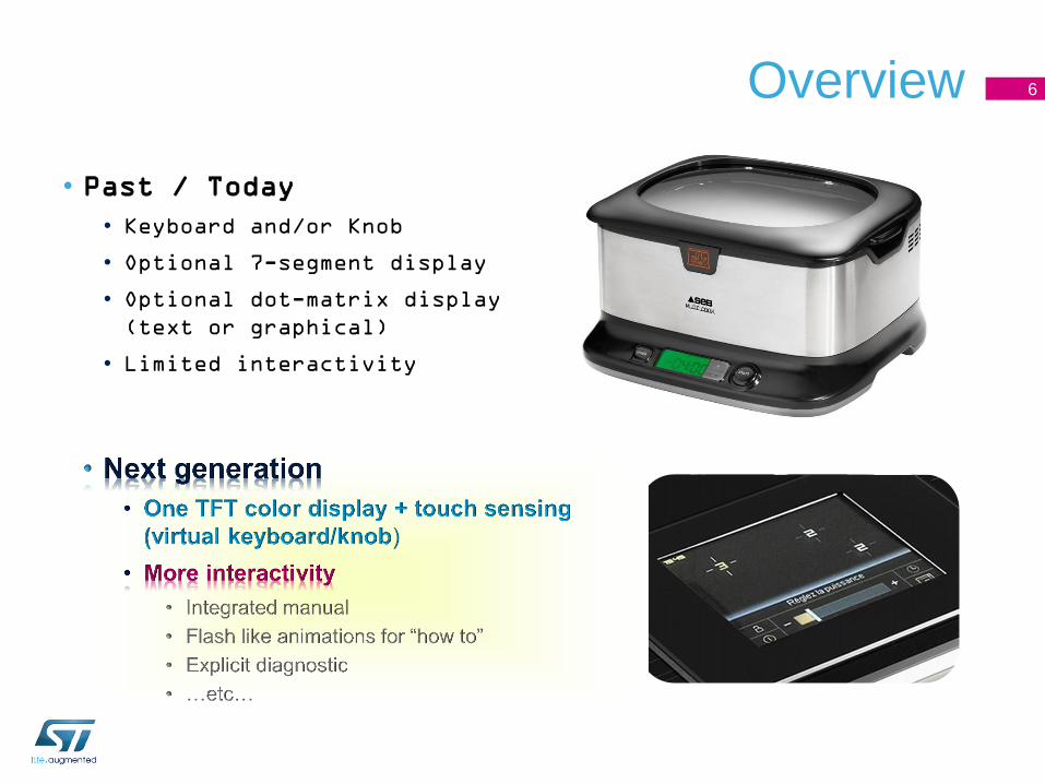
Overview
• Past / Today
• Keyboard and/or Knob
• Optional 7-segment display
• Optional dot-matrix display
(text or graphical)
• Limited interactivity
6

Display needs
• For home appliance
• Display size and form factor will be very different from an equipment to another
• In most of them we shall not be above 6~7 inches
• iPad 2 display is 132PPI (pixels per inch) and can go up to 160 or even more
(retina display)
• 7” 16:9 display represents 800x480 ~384kpix @130PPI (1024x576 @160PPI)
7
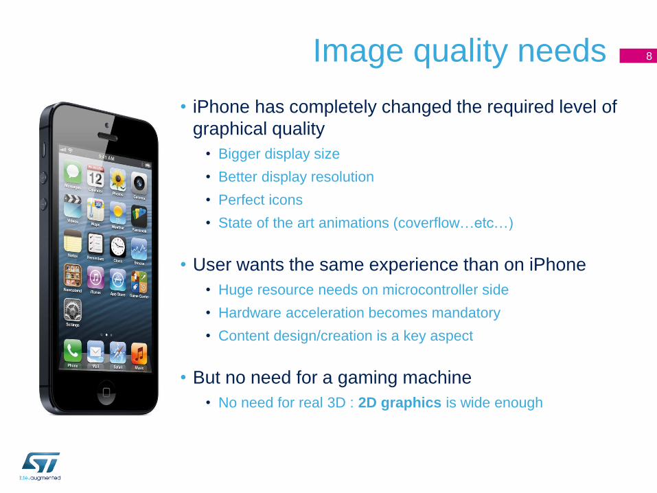
Image quality needs
• iPhone has completely changed the required level of
graphical quality
• Bigger display size
• Better display resolution
• Perfect icons
• State of the art animations (coverflow…etc…)
• User wants the same experience than on iPhone
• Huge resource needs on microcontroller side
• Hardware acceleration becomes mandatory
• Content design/creation is a key aspect
• But no need for a gaming machine
• No need for real 3D : 2D graphics is wide enough
8

From ones and zeros to image display 9
Font 1
Text 1
Step 2 : Display the frame buffer
• The frame buffer is transferred to the display through a
dedicated hardware interface
• Graphical oriented microcontroller are offering a TFT
controller to drive directly the display
• The frame buffer must be sent at 60fps to have a perfect
image color and stability (independently from the animation
fps)
Step 1 : Create the content in a frame buffer
• The frame buffer is build by composing graphical primitive
• This operation is done by the CPU running a graphical
library software
• It can be accelerated by a dedicated hardware used with
the CPU through the graphical library
• More often the frame buffer can be updated, more fluent
will be the animations (frames per second / fps)
Next Prev

STM32F4x9 Architecture
• TFT controller allows the interfacing
• Chrome-ART (DMA2D) provides a true HW graphical acceleration
• DMA2D offloads the CPU for operations like rectangle filling, rectangle
copy (with or without pixel format conversion), and image blending
• DMA2D goes faster than the CPU for the equivalent operation
TFT
Controller
Internal
Flash
Internal
SRAM
External
Memory
Controller
Chrom-ART
Accelerator
(DMA2D) Cortex-M4
Bus Matrix
External
memory
10

Implementation examples and
resources requirements
11
11
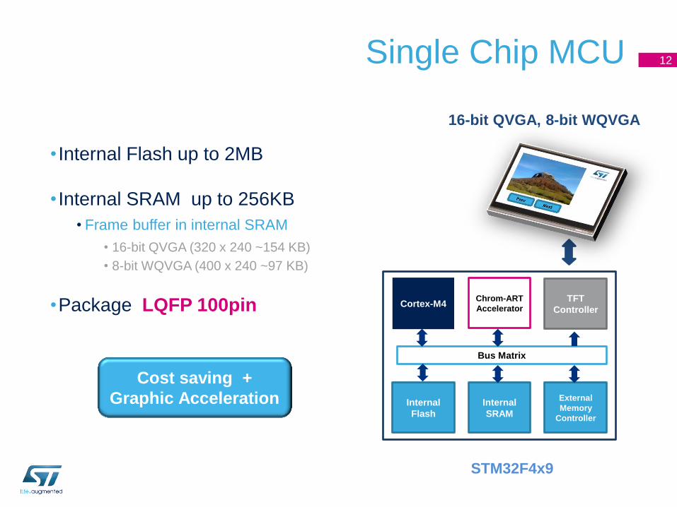
Single Chip MCU
• Internal Flash up to 2MB
• Internal SRAM up to 256KB
• Frame buffer in internal SRAM
• 16-bit QVGA (320 x 240 ~154 KB)
• 8-bit WQVGA (400 x 240 ~97 KB)
•Package LQFP 100pin
16-bit QVGA, 8-bit WQVGA
STM32F4x9
Cost saving +
Graphic Acceleration
TFT
Controller
Internal
Flash
Internal
SRAM
External
Memory
Controller
Chrom-ART
Accelerator Cortex-M4
Bus Matrix
12

MCU with External Memory
• Internal Flash up to 2MB
• Internal SRAM up to 256KB
•External Memory for frame buffer
• 16-bit or 32-bit SDRAM / SRAM
•Package: LQFP 144pin, up to 208.
13
Up to SVGA ( 800x600 )
STM32F4x9
Unique Graphical Capability
and
Flexible architecture
TFT
Controller
Internal
Flash
Internal
SRAM
External
Memory
Controller
Chrom-ART
Accelerator Cortex-M4
Bus Matrix
SDRAM

Which package to use depending on the
variant targeted?
Variant TFT Controller External Memory - SDRAM STM32F4x9 package
High-End Yes 32-bit LQFP208/BGA216
Mid-End Yes 16-bit LQFP144/
BGA176 / LQFP176
Low-End
No No LQFP100/LQFP144
Yes No LQFP100/LQFP144
SDRAM devices example: • MT48LC4M16A2P-7E : 64Mb
• MT48LC16M16A2P-7E : 256Mb
14

F4 discovery demo application
• Open the demo project in IAR EWARM.
…\Projects\Demonstration\EWARM_Demo\STM32F429I-Discovery_Demo.eww
• Build the project (F7) and debug (Ctrl-D) – this may take around one
minute and run (F5).
• Every push of USER button will switch to next demonstration.
15
The Discovery kit is present for you, you can keep it after
the seminar.
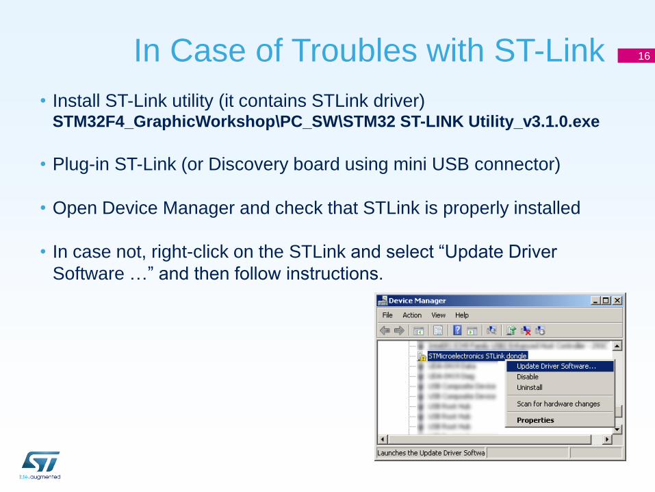
In Case of Troubles with ST-Link
• Install ST-Link utility (it contains STLink driver) STM32F4_GraphicWorkshop\PC_SW\STM32 ST-LINK Utility_v3.1.0.exe
• Plug-in ST-Link (or Discovery board using mini USB connector)
• Open Device Manager and check that STLink is properly installed
• In case not, right-click on the STLink and select “Update Driver
Software …” and then follow instructions.
16

F4 discovery demo application 17
• You can follow the application on the discovery kit
• By pushing the USER button you can navigate to the next step of
example application
17
• Move forward by pushing
the USER button
• Embedded STLINK debugger

LCD-TFT Display Controller
(LTDC)
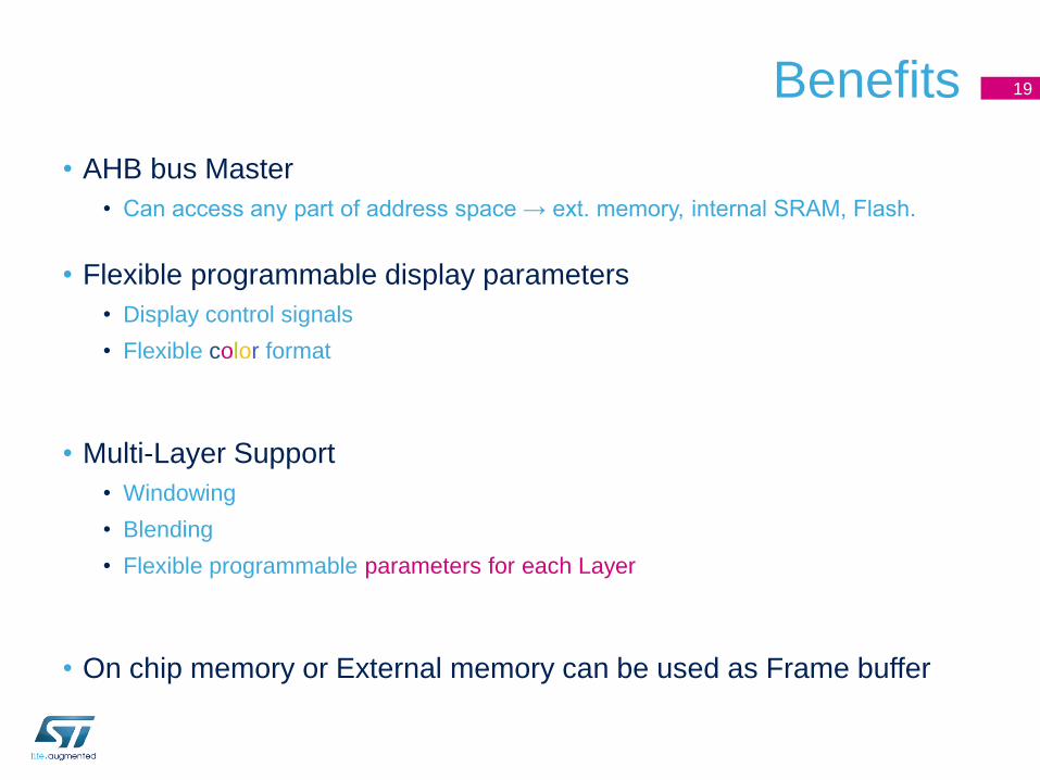
Benefits
• AHB bus Master
• Can access any part of address space → ext. memory, internal SRAM, Flash.
• Flexible programmable display parameters
• Display control signals
• Flexible color format
• Multi-Layer Support
• Windowing
• Blending
• Flexible programmable parameters for each Layer
• On chip memory or External memory can be used as Frame buffer
19

LCD-TFT architecture 20
AH
B M
as
ter
Inte
rfa
ce
LCD_G[7:0]
LCD_B[7:0]
Layer2
FIFO
64x32b
AH
B I
nte
rfa
ce
Co
nfi
gu
rati
on
an
d
sta
tus r
eg
iste
rs
LCD_CLK
LCD_HSYNC
LCD_VSYNC
LCD_DE
LCD_R[7:0]
LC
D
Pan
el Blending
PFC
PFC
Layer1
FIFO
64x32b
Synchronous
Timings
Generation
AP
B I
nte
rfac
e
Dithering
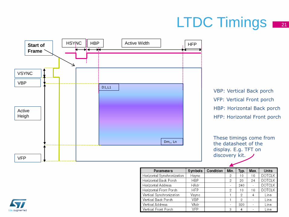
LTDC Timings 21
10/17/2013
D1,L1
Dm,, Ln
HFP HBP
VBP
VFP
VBP: Vertical Back porch
VFP: Vertical Front porch
HBP: Horizontal Back porch
HFP: Horizontal Front porch
Start of
Frame
VSYNC
HSYNC Active Width
Active
Heigh
These timings come from the datasheet of the display. E.g. TFT on discovery kit.

Frame Display
VSYNC Vertical Back
Porch (VBP)
LCD Lines Vertical Front
Porch (VFP)
22
HSYNC Horizontal
(VBP)
LCD Columns Horizontal
(HFP)
LCD_CLK
LCD RGBs
LCD Data Enable
1 Line
1 Frame
1 2 3 4 5 x x x x 480 x

Vertical/Horizontal transactions
• Horizontal transaction
23
• Vertical transaction
Start of Frame
Start of Scan Line

LCD basic timing signals
• LCDs require the following basic timing signals:
• VSYNC (Vertical Sync for TFT)
• Used to reset the LCD row pointer to the top of the display
• HSYNC (Horizontal sync for TFT)
• Used to reset the LCD column pointer to the edge of the display
• D0..Dxx (1 or more data lines)
• Data line
• LCDCLK (LCD pixel clock)
• Used to control panel refresh rate
• Some panels may require additional timing signals:
• LCD_DE
• LCD data Enable. Used to indicate valid data on the LCD data bus
• Other signals – some optional
• LCD power, backlight power, touchscreen
24
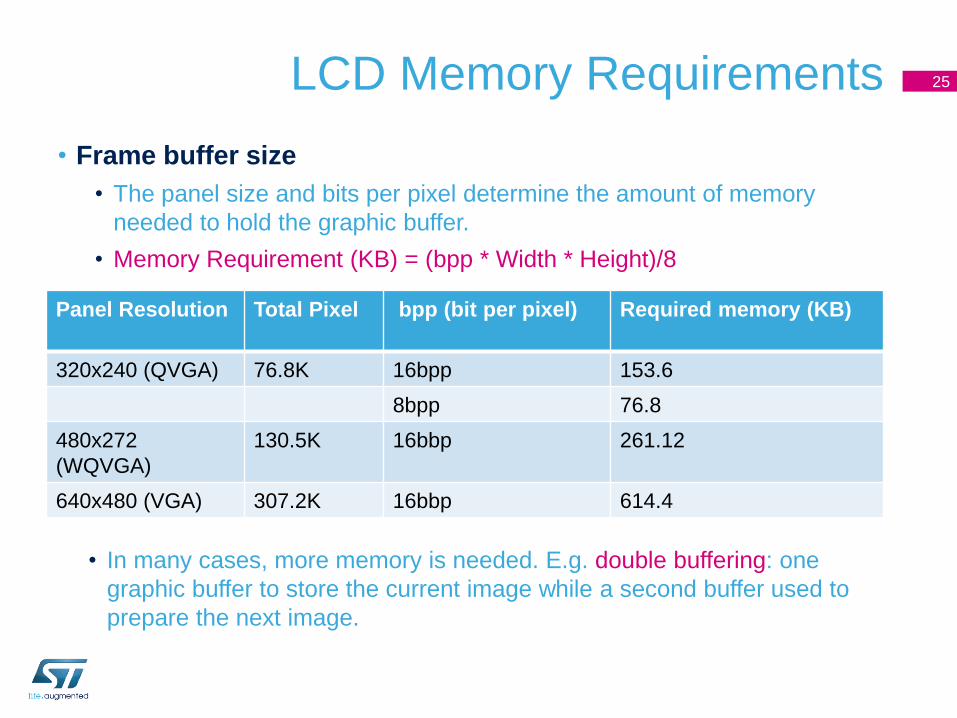
LCD Memory Requirements
• Frame buffer size
• The panel size and bits per pixel determine the amount of memory
needed to hold the graphic buffer.
• Memory Requirement (KB) = (bpp * Width * Height)/8
25
Panel Resolution Total Pixel
bpp (bit per pixel) Required memory (KB)
320x240 (QVGA) 76.8K 16bpp 153.6
8bpp 76.8
480x272
(WQVGA)
130.5K 16bbp 261.12
640x480 (VGA) 307.2K 16bbp 614.4
• In many cases, more memory is needed. E.g. double buffering: one
graphic buffer to store the current image while a second buffer used to
prepare the next image.

LTDC Clocks and reset
• Three clock domains:
• AHB clock domain (HCLK)
• To transfer data from the memories to the Layer FIFO and vise versa
• APB2 clock domain (PCLK2)
• To access the configuration and status registers
• The Pixel Clock domain (LCD_CLK)
• To generate LCD-TFT interface signals.
• LCD_CLK output should be configured following the panel requirements. The LCD_CLK is
configured through the PLLSAI
• LTDC Reset
• It is reset by setting the LTDCRST bit in the RCC_APB2RSTR register
26

LCD-TFT Signals
• The LCD-TFT IO pins not used by the application can be used for
other purposes.
27
LCD-TFT Signals Description
LCD_CLK Pixel Clock output
LCD_HSYNC Horizontal Synchronization
LCD_VSYNC Vertical Synchronization
LCD_DE Data Enable
LCD_R[7:0] 8-Bits Red data
LCD_G[7:0] 8-Bits Green data
LCD_B[7:0] 8-Bits Blue data
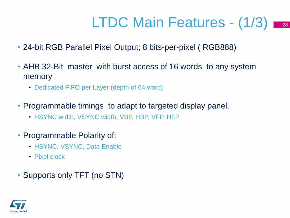
LTDC Main Features - (1/3)
• 24-bit RGB Parallel Pixel Output; 8 bits-per-pixel ( RGB888)
• AHB 32-Bit master with burst access of 16 words to any system
memory
• Dedicated FIFO per Layer (depth of 64 word)
• Programmable timings to adapt to targeted display panel.
• HSYNC width, VSYNC width, VBP, HBP, VFP, HFP
• Programmable Polarity of:
• HSYNC, VSYNC, Data Enable
• Pixel clock
• Supports only TFT (no STN)
28

LTDC Main Features - (2/3)
• Programmable display Size
• Supports up to 800 x 600 (SVGA)
• Programmable Background color
• 24-bit RGB, used for blending with bottom layer.
• Multi-Layer Support with blending, 2 layers + solid color background
• Dithering (2-bits per color channel (2,2,2 for RGB))
• Combination of adjacent pixels to simulate the desired shade
• Dithering is applicable for 18bit color displays, to simulate 24bit colors.
• Newly programmed values can be loaded immediately at run time or
during Vertical blanking
• 2 Interrupts generated on 4 event Flags
29
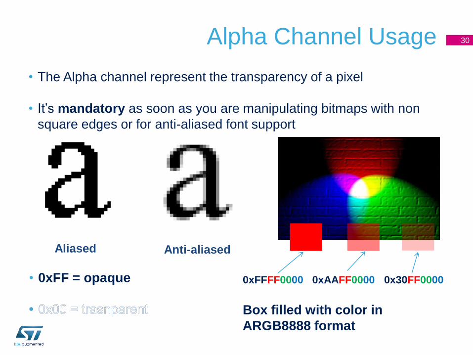
Alpha Channel Usage
• The Alpha channel represent the transparency of a pixel
• It’s mandatory as soon as you are manipulating bitmaps with non
square edges or for anti-aliased font support
30
Aliased Anti-aliased
• 0xFF = opaque 0xFFFF0000 0xAAFF0000 0x30FF0000
Box filled with color in
ARGB8888 format
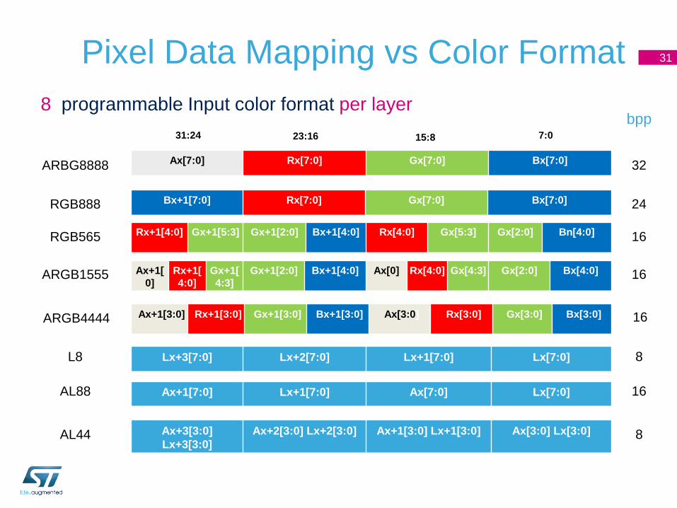
Pixel Data Mapping vs Color Format
Ax+1[3:0] Rx+1[3:0] Gx+1[3:0] Bx+1[3:0] Ax[3:0] Rx[3:0]
Gx[3:0] Bx[3:0]
31
7:0 15:8 23:16 31:24
ARBG8888
RGB888
ARGB4444
AL88 Ax+1[7:0] Lx+1[7:0] Ax[7:0] Lx[7:0]
Bx+1[7:0] Rx[7:0] Gx[7:0] Bx[7:0]
Ax[7:0] Rx[7:0] Gx[7:0] Bx[7:0]
Ax+3[3:0]
Lx+3[3:0]
Ax+2[3:0] Lx+2[3:0] Ax+1[3:0] Lx+1[3:0] Ax[3:0] Lx[3:0] AL44
Lx+3[7:0] Lx+2[7:0] Lx+1[7:0] Lx[7:0] L8
Ax+1[
0]
Rx+1[
4:0]
Gx+1[
4:3]
Gx+1[2:0] Bx+1[4:0] Ax[0] Rx[4:0] Gx[4:3] Gx[2:0] Bx[4:0] ARGB1555
Rx+1[4:0] Gx+1[5:3] Gx+1[2:0]
Bx+1[4:0] Rx[4:0] Gx[5:3] Gx[2:0] Bn[4:0] RGB565
32
24
16
16
16
8
16
8
bpp 8 programmable Input color format per layer
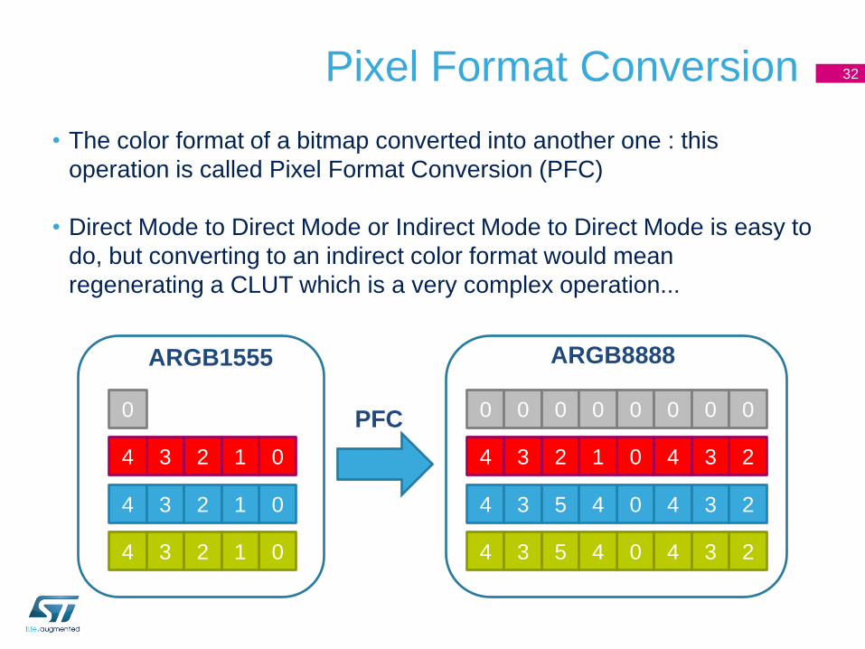
Pixel Format Conversion
• The color format of a bitmap converted into another one : this
operation is called Pixel Format Conversion (PFC)
• Direct Mode to Direct Mode or Indirect Mode to Direct Mode is easy to
do, but converting to an indirect color format would mean
regenerating a CLUT which is a very complex operation...
32
0 0 0 0 0 0 0 0
0 4 3 2 4 3 2 1
0 4 3 2 4 3 5 4
0 4 3 2 4 3 5 4
0
0 4 3 2 1
0 4 3 2 1
0 4 3 2 1
PFC
ARGB1555 ARGB8888

PFC - Direct color Mode 33
A R G B
32-bit per pixel
ARGB8888
24-bit per pixel
RGB888
16-bit per pixel
ARGB4444
ARGB1555
RGB565
Direct coding

PFC - Indirect color Mode 34
A R G B
8-bit per pixel
L8
AL44
A8
4-bit per pixel
L4
A4
16-bit per pixel
AL88
Indirect coding A R G B
A R G B
...
Color
LookUp Table
Index
A R G B
0x00
0x01
0xFF
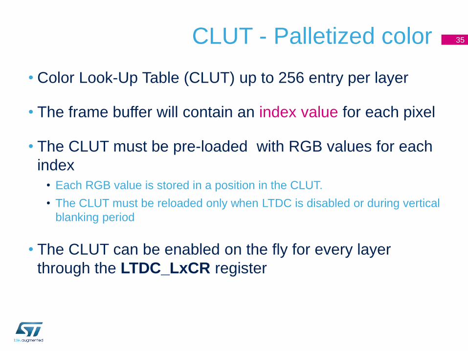
CLUT - Palletized color
• Color Look-Up Table (CLUT) up to 256 entry per layer
• The frame buffer will contain an index value for each pixel
• The CLUT must be pre-loaded with RGB values for each
index
• Each RGB value is stored in a position in the CLUT.
• The CLUT must be reloaded only when LTDC is disabled or during vertical
blanking period
• The CLUT can be enabled on the fly for every layer
through the LTDC_LxCR register
35

CLUT- Palletized
• The R, G and B values and their own respective address are
programmed through the LTDC_LxCLUTWR register.
• L8 and AL88 input pixel format, the CLUT has to be loaded by 256 colors
• AL44 input pixel format, the CLUT has to be loaded by 16 colors. The address of
each color must be filled by replicating the 4-bit L channel to 8-bit.
• L0 (indexed color 0), at address 0x00,
• L1, at address 0x11….
• L2, at address 0x22
36
Source - wikipedia.org
Indexed 256 - L8 Indexed 16 – L4 RGB888
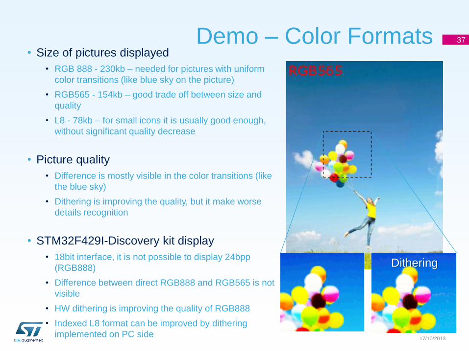
Demo – Color Formats 37
37
• Size of pictures displayed
• RGB 888 - 230kb – needed for pictures with uniform
color transitions (like blue sky on the picture)
• RGB565 - 154kb – good trade off between size and
quality
• L8 - 78kb – for small icons it is usually good enough,
without significant quality decrease
• Picture quality
• Difference is mostly visible in the color transitions (like
the blue sky)
• Dithering is improving the quality, but it make worse
details recognition
• STM32F429I-Discovery kit display
• 18bit interface, it is not possible to display 24bpp
(RGB888)
• Difference between direct RGB888 and RGB565 is not
visible
• HW dithering is improving the quality of RGB888
• Indexed L8 format can be improved by dithering
implemented on PC side
17/10/2013
Dithering

Layer Programmable Parameters:
Window • Window position and size
• The first and last visible Pixel are configured in the LTDC_LxWHPCR register.
• The first and last visible line are configured in the LTDC_LxWVPCR
38
START_POS_X
START_POS_Y
END_POS_Y
END_X_POS
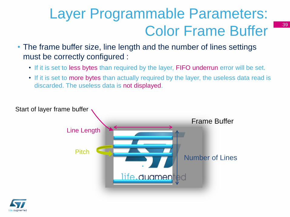
Layer Programmable Parameters:
Color Frame Buffer • The frame buffer size, line length and the number of lines settings
must be correctly configured :
• If it is set to less bytes than required by the layer, FIFO underrun error will be set.
• If it is set to more bytes than actually required by the layer, the useless data read is
discarded. The useless data is not displayed.
39
Line Length
Number of Lines .
.
Pitch
Frame Buffer
Start of layer frame buffer
Layer Programmable Parameters:
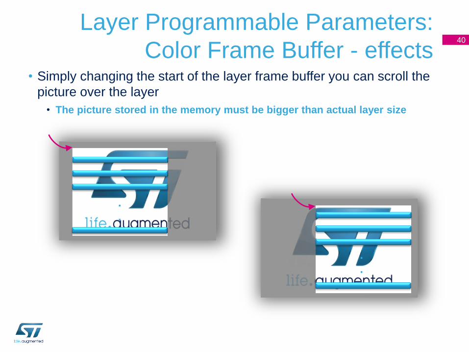
Color Frame Buffer - effects • Simply changing the start of the layer frame buffer you can scroll the
picture over the layer
• The picture stored in the memory must be bigger than actual layer size
40
.
.
.
.

Demo - Moving layer
• Just by changing the layer buffer address
you can move the visible layer over a
bitmap which is bigger than the layer.
41
41
400
320
LTDC_Layer_InitStruct.LTDC_CFBStartAdress =
(uint32_t)Image + 3 * (offsetH + (offsetV * Image_width));
• Horizontal
scroll
• Vertical scroll • Bytes per pixel
• Base address of
image in memory 240
320
Layer Programmable Parameters:
Multi-layer blending • Blending is always active using alpha value
• Blending factors are configured through the LTDC_LxBFCR register
• Fixed Constant alpha
• Alpha pixel multiplied by the Constant Alpha
• The blending order is fixed and it is bottom up.
• Programmable Background Color for the bottom layer
42
Layer 2 Layer 1
Solid color
background

Blending – Example 1
• Layer 1 blending with background
• Background is black
• Layer 2 is disabled.
43
75%
25%
0%
50%
100%

Blending – Example 2
• Layer 1 and Layer 2 blending
• Background color is black
• Layer 1 Constant Alpha set to 100 %
• Layer 2 Constant Alpha is set to:
44
75 %
25 %
0 %
50 %
100%
Demo – Two Layers
• Example is using two layers
• Layer 1 – static background picture
• Layer 2 – moving ST logo with alpha channel
• ST logo is moved using layer 2 parameters only, no load of CPU
• Blending is done directly by Constant Alpha parameter, no load of
CPU, done by LTDC controller directly
45
45
Layer Programmable Parameters:
Color Keying • Transparent color (RGB) can be defined for each layer in the
LTDC_LxCKCR register
• When the Color Keying is enabled, the current pixels is compared to
the color key. If they match for the programmed RGB value, all
channels (ARGB) of that pixel are set to 0.
• Color Keying can be enabled on the fly for each layer in the
LTDC_LxCR regiser
46

Demo - Color Keying
• Example is using two layers
• Layer 1 – background picture “blue sky”
• Layer 2 – ST logo with white background color
• Keying color is set to WHITE
• Disturbing artifacts can be removed by pre-processing using tools
like Photoshop or Gimp, but quality of result is usually depending
on the background anyway
• Best suitable for rectangular graphical objects
• Not optimal for photos – use alpha channel blending instead
47
47
Layer Programmable Parameters:
Default Color
• Default Color • The default color ( ARGB) is used outside the defined layer
window or when a layer is disabled.
• The default color is configured through the LTDC_LxDCCR
register.
• To bypass the default color, set the blending factor to transparent
Alpha
• Tricky use case: • Layer 1 is enabled
• Layer 2 is disabled, with default color black.
• If blending factor is set to ConstAlpha=0xFF, No image will be
displayed. Only black window that will be displayed ( default color
of Layer2 is black).
48
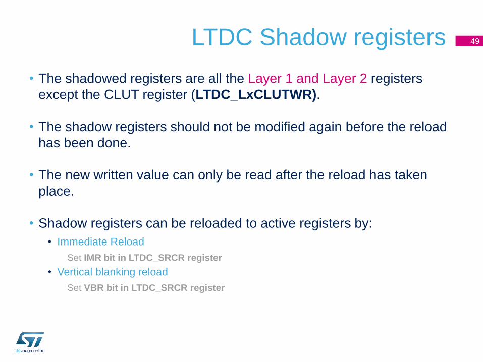
LTDC Shadow registers
• The shadowed registers are all the Layer 1 and Layer 2 registers
except the CLUT register (LTDC_LxCLUTWR).
• The shadow registers should not be modified again before the reload
has been done.
• The new written value can only be read after the reload has taken
place.
• Shadow registers can be reloaded to active registers by:
• Immediate Reload
Set IMR bit in LTDC_SRCR register
• Vertical blanking reload
Set VBR bit in LTDC_SRCR register
49
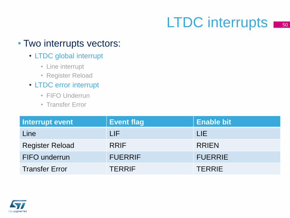
LTDC interrupts
• Two interrupts vectors:
• LTDC global interrupt
• Line interrupt
• Register Reload
• LTDC error interrupt
• FIFO Underrun
• Transfer Error
50
Interrupt event Event flag Enable bit
Line LIF LIE
Register Reload RRIF RRIEN
FIFO underrun FUERRIF FUERRIE
Transfer Error TERRIF TERRIE
Chrom-ART Accelerator™ STM32F4 Graphic Accelerator (DMA2D)

Overview
Font 1
Text 1
Step 2 : Display the frame buffer
• The frame buffer is transferred to the display through a
dedicated hardware interface
• Graphical oriented microcontroller are offering a TFT
controller to drive directly the display
• The frame buffer must be sent at 60fps to have a perfect
image color and stability (independently from the animation
fps)
Step 1 : Create the content in a frame buffer
• The frame buffer is build by composing graphical primitive
• This operation is done by the CPU running a graphical
library software
• It can be accelerated by a dedicated hardware used with
the CPU through the graphical library
• More often the frame buffer can be updated, more fluent
will be the animations (animation fps)
Next Prev
52

Graphical content creation
53

Creating something « cool »
• How the frame buffer is generated for creating a “cool” graphical
interface to be displayed through the TFT controller ?
54
-5°C
21°C
62%
Temperature
Humidity
ARMED
14:21

Frame buffer construction
• The frame buffer is generated drawing successively all the graphic
objects
55
-5°C
21°C
62%
Temperature
Humidity
ARMED
14:21

Frame buffer generation needs 56
• The resulting frame buffer is an uncompressed bitmap of the size of
the screen.
• Each object to be drawn can be
• A Bitmap with its own color coding (different from the final one), compressed or not
• A Vector Description (a line, a circle with a texture...etc....)
• (A Text)
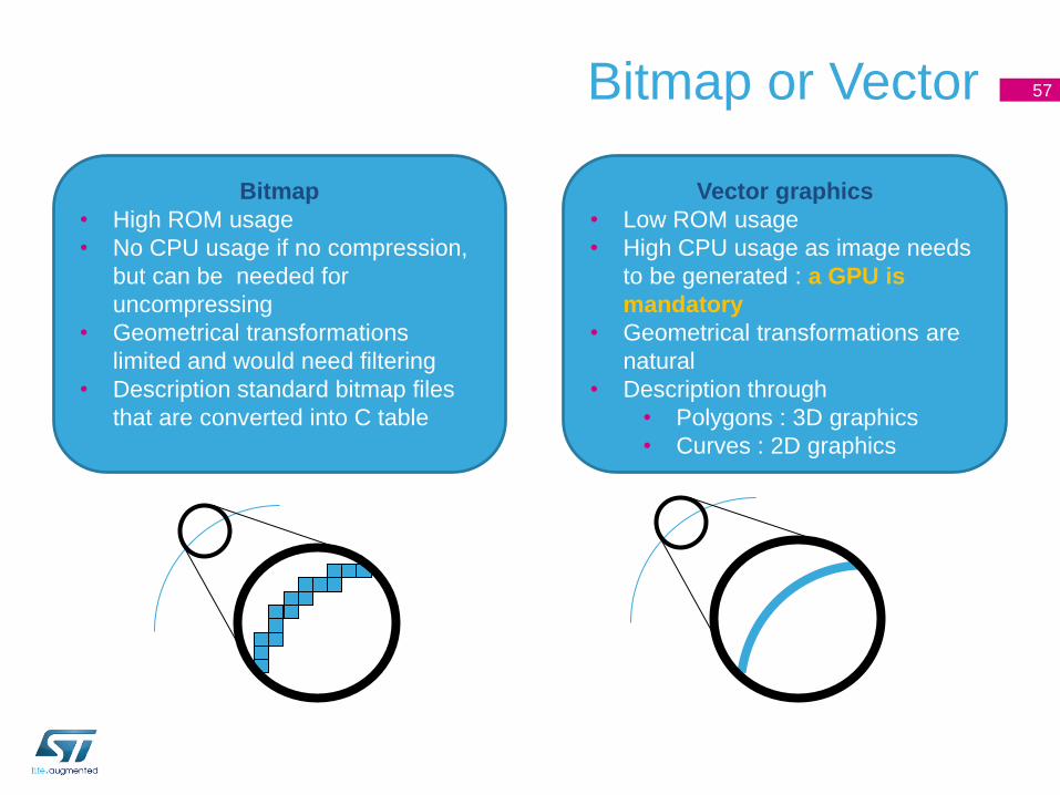
Bitmap or Vector 57
Bitmap
• High ROM usage
• No CPU usage if no compression,
but can be needed for
uncompressing
• Geometrical transformations
limited and would need filtering
• Description standard bitmap files
that are converted into C table
Vector graphics
• Low ROM usage
• High CPU usage as image needs
to be generated : a GPU is
mandatory
• Geometrical transformations are
natural
• Description through
• Polygons : 3D graphics
• Curves : 2D graphics

Example of vector pipeline 58

STM32F42x/F43x Architecture
• TFT controller allows the interfacing
• DMA2D provides a true graphical acceleration
• DMA2D offloads the CPU for operations like rectangle filling, rectangle
copy (with or without pixel format conversion), and image blending
• DMA2D goes faster than the CPU for the equivalent operation
TFT
Controller
Internal
Flash
Internal
SRAM
External
Memory
Controller
Chrom-ART
Accelerator Cortex-M4
Bus Matrix
59

Bitmaps
60
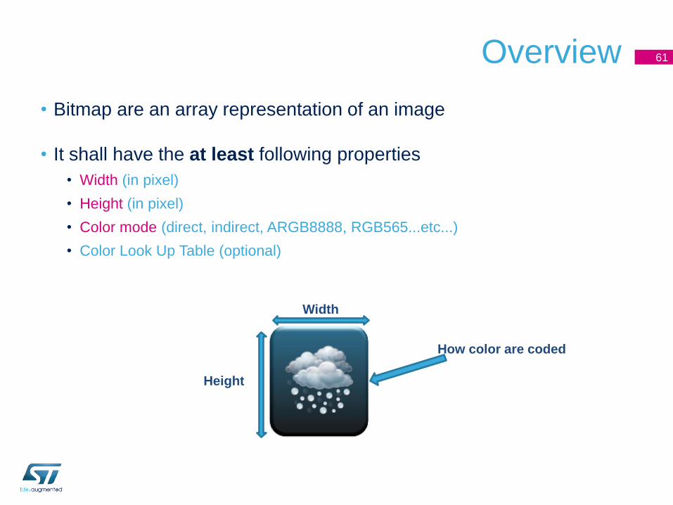
Overview
• Bitmap are an array representation of an image
• It shall have the at least following properties
• Width (in pixel)
• Height (in pixel)
• Color mode (direct, indirect, ARGB8888, RGB565...etc...)
• Color Look Up Table (optional)
61
Width
Height
How color are coded

Blending
• Blending consist in drawing an image onto another respecting the
transparency information
• As a consequence blending implies to read 2 sources, then blend
then write to the destination
62
Not Blended
Blended
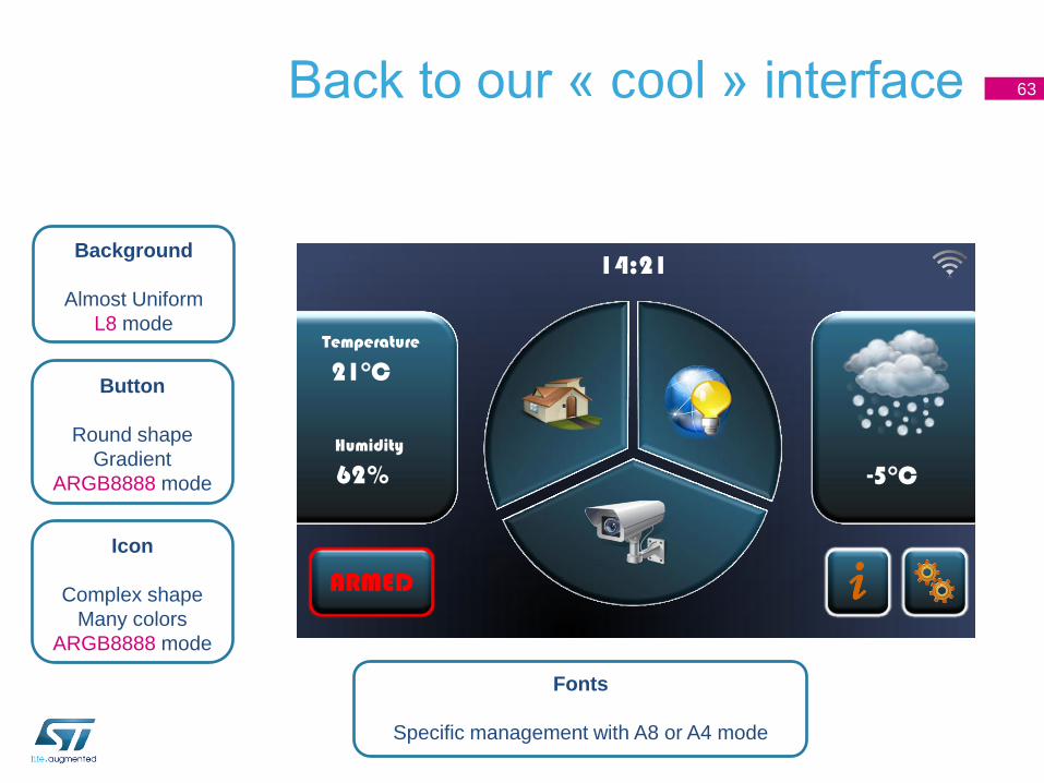
Back to our « cool » interface 63
-5°C
21°C
62%
Temperature
Humidity
ARMED
14:21 Background
Almost Uniform
L8 mode
Button
Round shape
Gradient
ARGB8888 mode
Icon
Complex shape
Many colors
ARGB8888 mode
Fonts
Specific management with A8 or A4 mode

Demo – Content Creation
• Moving successively graphical elements from internal FLASH into
the frame buffer by Chrome-ART
64
64
ARMED
ARMED
DMA2D source
parameters:
Location in
memory, width,
height, pixel format
DMA2D destination
parameters:
Location in buffer,
width, height, pixel
format, line offset
DMA2D
foreground
background
output
FLASH content

Font management
• Bitmap fonts are managed only using alpha channel (transparency)
65
ROMed character bitmap
(A8 or A4) Generated character bitmap
with color information
(ARGB8888, ARGB1555, ARGB4444)
or
(RGB888, RGB565)
PFC
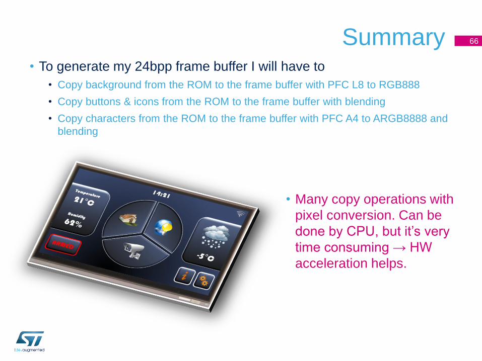
Summary • To generate my 24bpp frame buffer I will have to
• Copy background from the ROM to the frame buffer with PFC L8 to RGB888
• Copy buttons & icons from the ROM to the frame buffer with blending
• Copy characters from the ROM to the frame buffer with PFC A4 to ARGB8888 and
blending
66
• Many copy operations with
pixel conversion. Can be
done by CPU, but it’s very
time consuming → HW
acceleration helps.

Chrom-ART Accelerator
(DMA2D)
67
Overview
• The Chrom-ART combines both a DMA2D and graphical oriented
functionality for image blending and pixel format conversion.
• To offload the CPU of raw data copy, the Chrom-ART is able to copy
a part of a graphic content into another part of a graphic content, or
simply to fill an part of a graphic content with a specified color.
• In addition to raw data copy, additional functionality can be added
such as image format conversion or image blending (image mixing
with some transparency).
68

TFT
Controller
Internal
Flash
Internal
SRAM
External
Memory
Controller
Chrom-ART
Accelerator Cortex-M4
Bus Matrix
Typical data flow 69
Creation of an object in a memory device by the Chrom-ART
Update/Creation of the frame buffer in the external RAM by the Chrom-ART
TFT controller data flow
Chrom-ART features
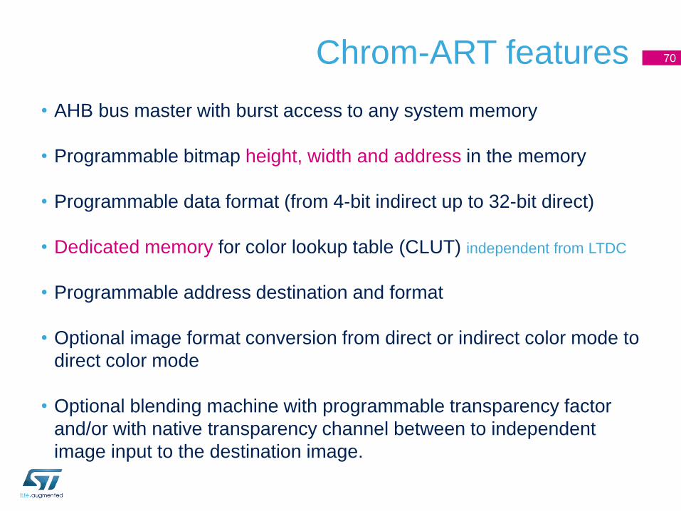
• AHB bus master with burst access to any system memory
• Programmable bitmap height, width and address in the memory
• Programmable data format (from 4-bit indirect up to 32-bit direct)
• Dedicated memory for color lookup table (CLUT) independent from LTDC
• Programmable address destination and format
• Optional image format conversion from direct or indirect color mode to
direct color mode
• Optional blending machine with programmable transparency factor
and/or with native transparency channel between to independent
image input to the destination image.
70
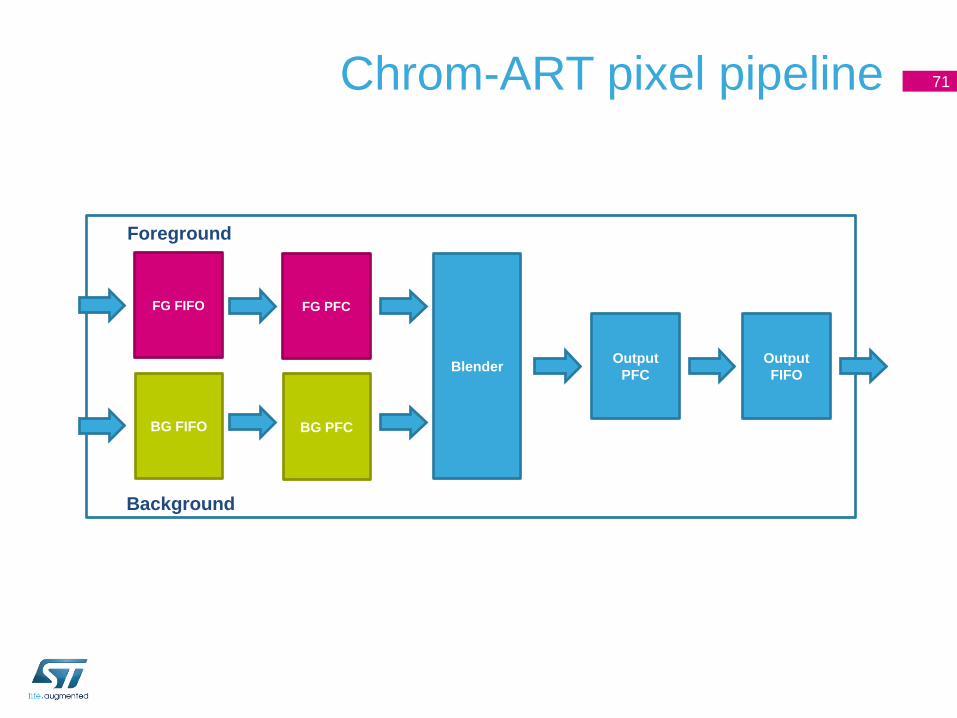
Chrom-ART pixel pipeline 71
Output
PFC
BG FIFO
FG FIFO
BG PFC
FG PFC
Output
FIFO Blender
Foreground
Background

-5°C
21°C
62%
Temperature
Humidity
ARMED
14:21
Bitmap parameter 72
Width
Height
Original_Width
Original_Address Address
Original_Height
Address = Original_Address + (X + Original_Width * Y) * BPP
LineOffset = Original_Width - Width
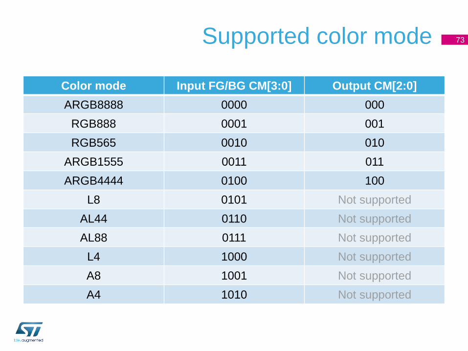
Supported color mode
Color mode Input FG/BG CM[3:0] Output CM[2:0]
ARGB8888 0000 000
RGB888 0001 001
RGB565 0010 010
ARGB1555 0011 011
ARGB4444 0100 100
L8 0101 Not supported
AL44 0110 Not supported
AL88 0111 Not supported
L4 1000 Not supported
A8 1001 Not supported
A4 1010 Not supported
73

CLUT management
• When an indirect color mode L8, AL44 or AL88 is used, the bitmap
CLUT must be loaded into the Chrom-ART
• Each FG and BG has its own dedicated memory for CLUT.
• The CLUT can be loaded manually when no Chrom-ART operation
are on going
• The CLUT can be loaded automatically configuring the CLUT format
(24-bit or 32-bit), the CLUT size and the CLUT address and setting
the CLUT Start bit
74

Supported operations
• 4 functional modes are supported
• Register to memory : the destination bitmap is filled with the specified output color
• Memory to memory : the data are fetch through the FG and are written to the
destination bitmap without any color format modification (no PFC)
• Memory to memory with PFC : the data are fetch through the FG and are written
to the destination bitmap after being converted into the destination color format
(PFC)
• Memory to memory with PFC and blending : the data are fetched through the
FG and the BG, are converted, are blended together and are written to the
destination bitmap
• Once configured, the Chrom-ART is launched setting the Start bit
• The operation can be either suspended through the Suspend bit or
aborted through the abort bit
75

Alpha modulation
• When the PFC is activated the Alpha value of the pixel can be
modified as follow
• Kept as it is
• Replaced by a fixed one
• Replaced by the current one multiplied
by the fixed one
• This allows to perform easily fade in/out animations
76

Line Watermark
• For synchronization purpose, an interrupt can be generated when a
specified line has been written by the Chrom-ART into the memory
• The line number is defined by the filed LW[15:0] of the DMA2D_LWR
register
77
Line
watermark
interrupt DMA2D
transfer
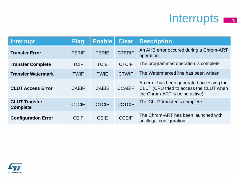
Interrupts
Interrupt Flag Enable Clear Description
Transfer Error TERIF TERIE CTERIF An AHB error occured during a Chrom-ART
operation
Transfer Complete TCIF TCIE CTCIF The programmed operation is complete
Transfer Watermark TWIF TWIE CTWIF The Watermarked line has been written
CLUT Access Error CAEIF CAEIE CCAEIF
An error has been generated accessing the
CLUT (CPU tried to access the CLUT when
the Chrom-ART is being active)
CLUT Transfer
Complete CTCIF CTCIE CCTCIF
The CLUT transfer is complete
Configuration Error CEIF CEIE CCEIF The Chrom-ART has been launched with
an illegal configuration
78
Chrom-ART
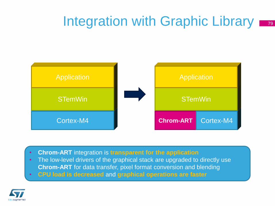
Integration with Graphic Library 79
Cortex-M4
STemWin
Application
Cortex-M4
STemWin
Application
• Chrom-ART integration is transparent for the application
• The low-level drivers of the graphical stack are upgraded to directly use
Chrom-ART for data transfer, pixel format conversion and blending
• CPU load is decreased and graphical operations are faster

STM32 Solution for Graphics
• STM32 offers a unique graphical capability in the Cortex-M based
MCU perimeter
• Real TFT Controller for optimum display control
• External memory interface to connect both Flash for static content and SRAM or
SDRAM for dynamic content and frame buffer
• On-chip hardware acceleration deeply coupled with graphical library
• Standard graphical library taking advantage of on-chip graphical acceleration
80

www.st.com/stm32f4


![INDEX [qualtekusa.com]qualtekusa.com/PDFs/Heatshrink-BROCHURE.pdfINDEX General Information Page HEAT ... (3X) CPX300, Deray-I 3000 SFTW-203 FIT 321V HS101 SR GSHS-3635 Q2-F4X 16 RP-4800](https://static.documents.pub/doc/80x56/5b27fb857f8b9a5f2d8b6a7b/index-general-information-page-heat-3x-cpx300-deray-i-3000-sftw-203-fit.jpg)


