Page 1
University of Central Florida University of Central Florida
STARS STARS
Electronic Theses and Dissertations, 2004-2019
2009
Embedded Magnetics For Power System On Chip (psoc) Embedded Magnetics For Power System On Chip (psoc)
Jian Lu University of Central Florida
Part of the Electrical and Electronics Commons
Find similar works at: https://stars.library.ucf.edu/etd
University of Central Florida Libraries http://library.ucf.edu
This Doctoral Dissertation (Open Access) is brought to you for free and open access by STARS. It has been accepted
for inclusion in Electronic Theses and Dissertations, 2004-2019 by an authorized administrator of STARS. For more
information, please contact [email protected] .
STARS Citation STARS Citation Lu, Jian, "Embedded Magnetics For Power System On Chip (psoc)" (2009). Electronic Theses and Dissertations, 2004-2019. 4010. https://stars.library.ucf.edu/etd/4010
Page 2
EMBEDDED MAGNETICS FOR POWER SYSTEM ON CHIP (PSoC)
by
JIAN LU M.S.E.E, University of Central Florida, 2007
B.S.E.E, Nanjing University of Science & Technology, Nanjing, China, 2003
A dissertation submitted in partial fulfillment of the requirements for the degree of Doctor of Philosophy
in the School of Electrical Engineering and Computer Science in the College of Engineering and Computer Science
at the University of Central Florida Orlando, Florida
Fall 2009
Major Professor: Z. John Shen
Page 4
iii
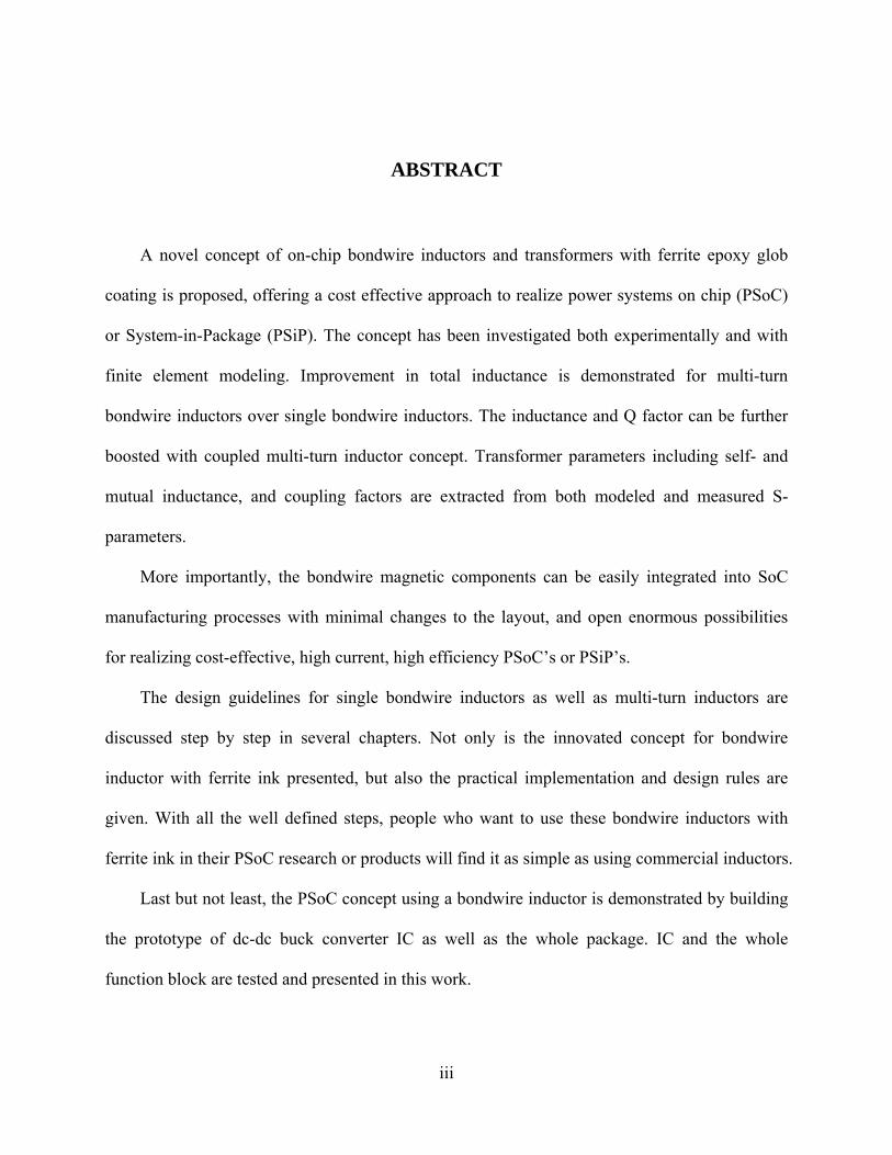
ABSTRACT
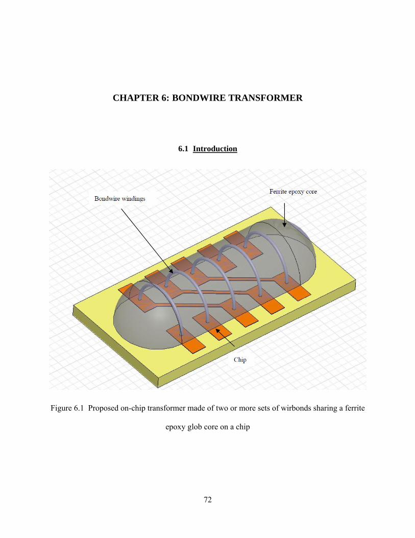
A novel concept of on-chip bondwire inductors and transformers with ferrite epoxy glob
coating is proposed, offering a cost effective approach to realize power systems on chip (PSoC)
or System-in-Package (PSiP). The concept has been investigated both experimentally and with
finite element modeling. Improvement in total inductance is demonstrated for multi-turn
bondwire inductors over single bondwire inductors. The inductance and Q factor can be further
boosted with coupled multi-turn inductor concept. Transformer parameters including self- and
mutual inductance, and coupling factors are extracted from both modeled and measured S-
parameters.
More importantly, the bondwire magnetic components can be easily integrated into SoC
manufacturing processes with minimal changes to the layout, and open enormous possibilities
for realizing cost-effective, high current, high efficiency PSoC’s or PSiP’s.
The design guidelines for single bondwire inductors as well as multi-turn inductors are
discussed step by step in several chapters. Not only is the innovated concept for bondwire
inductor with ferrite ink presented, but also the practical implementation and design rules are
given. With all the well defined steps, people who want to use these bondwire inductors with
ferrite ink in their PSoC research or products will find it as simple as using commercial inductors.
Last but not least, the PSoC concept using a bondwire inductor is demonstrated by building
the prototype of dc-dc buck converter IC as well as the whole package. IC and the whole
function block are tested and presented in this work.
Page 5
iv
ACKNOWLEDGMENTS
I would like to express my gratitude to my advisor, Dr. Z. John Shen, for his guidance,
advice and support throughout this work. I am grateful for the opportunity to work with him. He
is the one who lead me into the fantastic world of power electronics. I benefited a lot from the
knowledge and skills he taught me.
I would like to take this opportunity to thank other committee members: Dr. Thomas X. Wu,
Dr. Kalpathy B. Sundaram, Dr. Xun Gong and Dr. Osama Abdel-Rahman. They spent their
valuable time and gave a lot of useful suggestions for my research.
I will miss my friends in PSRL, namely: Hongwei Jia, Shan Sun, Yali Xiong, Boyi Yang,
Yue Fu, Xu Cheng, Mi Dong, Xuexin Wang, Qian Zhang, Patrick Shea, Brain Grummel,
Andreas Arias and Matt Landowski. We had a great time working together. I am also very
grateful to Dr Ger Hurley from National University of Ireland and my basketball pal Brian
Chang, who spent a lot of time proofreading my dissertation and helped me to correct my
grammar errors. And sincere gratitude goes to my friends in UCF who make my life in America
colorful, namely, Yu Lao, Li Chen, Lina Guo, Liangbin Yao, Yan Tang, Lifang Lou, Jun Fan,
Baiyun Chen, Shaohua Lin, Ji Chen, Jun Huang, Mingda Zhang, Xin Gu, Jun Xia, Zhibing Ge,
Jiangmin Chunyu, You Li, Jun Ma.
Page 6
v
I would like to express my thanks to my mother, Cuiqin Qu, my father, Huixiang Lu for
their mental support throughout my entire graduate works. Last, but not least, I owe the biggest
thanks to my wife Hongxia Tang for unconditional love, support and patience she provided me
while working on this project. Without her support, I would not have completed this degree.
Page 8
vii
TABLE OF CONTENTS
LIST OF FIGURES ....................................................................................................................... ix
LIST OF TABLES....................................................................................................................... xiv
LIST OF ACRONYMS/ABBREVIATIONS............................................................................... xv
CHAPTER 1: INTRODUCTION................................................................................................... 1
1.1 Power SoC & SiP Motivation......................................................................................... 1
1.2 Organization of This Thesis............................................................................................ 7
CHAPTER 2: STATE OF THE ARTS........................................................................................... 9
2.1 CMOS On-Chip Magnetics............................................................................................. 9
2.2 Thin Film On-Chip Magnetics...................................................................................... 12
2.3 PCB Magnetics ............................................................................................................. 15
2.4 LTCC Magnetics........................................................................................................... 16
2.5 Bondwire Magnetics ..................................................................................................... 20
2.6 Discussions ................................................................................................................... 23
CHAPTER 3: RESEARCH OBJECTIVE AND APPROACH.................................................... 25
3.1 Proposed Bondwire Magnetics Concept....................................................................... 25
3.2 Finite Element Modeling Tools .................................................................................... 28
CHAPTER 4: BONDWIRE INDUCTOR.................................................................................... 32
4.1 Proposed Bondwire Inductor ........................................................................................ 32
4.2 Experiment Results ....................................................................................................... 37
4.3 Design Guidelines and Discussions .............................................................................. 45
CHAPTER 5: BONDWIRE MULTI-TURN INDUCTORS........................................................ 51
Page 9
viii
5.1 Bondwire Multi-Turn Inductors.................................................................................... 51
5.2 Experiment Results ....................................................................................................... 62
5.3 Design Guidelines and Discussion................................................................................ 69
CHAPTER 6: BONDWIRE TRANSFORMER ........................................................................... 72
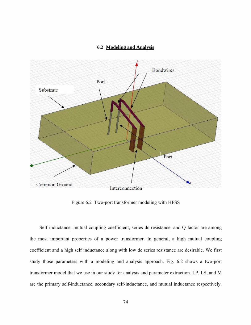
6.1 Introduction................................................................................................................... 72
6.2 Modeling and Analysis ................................................................................................. 74
6.3 Experiment Results ....................................................................................................... 79
CHAPTER 7: POWER SOC DESIGN......................................................................................... 89
7.1 Introduction................................................................................................................... 89
7.2 Converter IC Design ..................................................................................................... 89
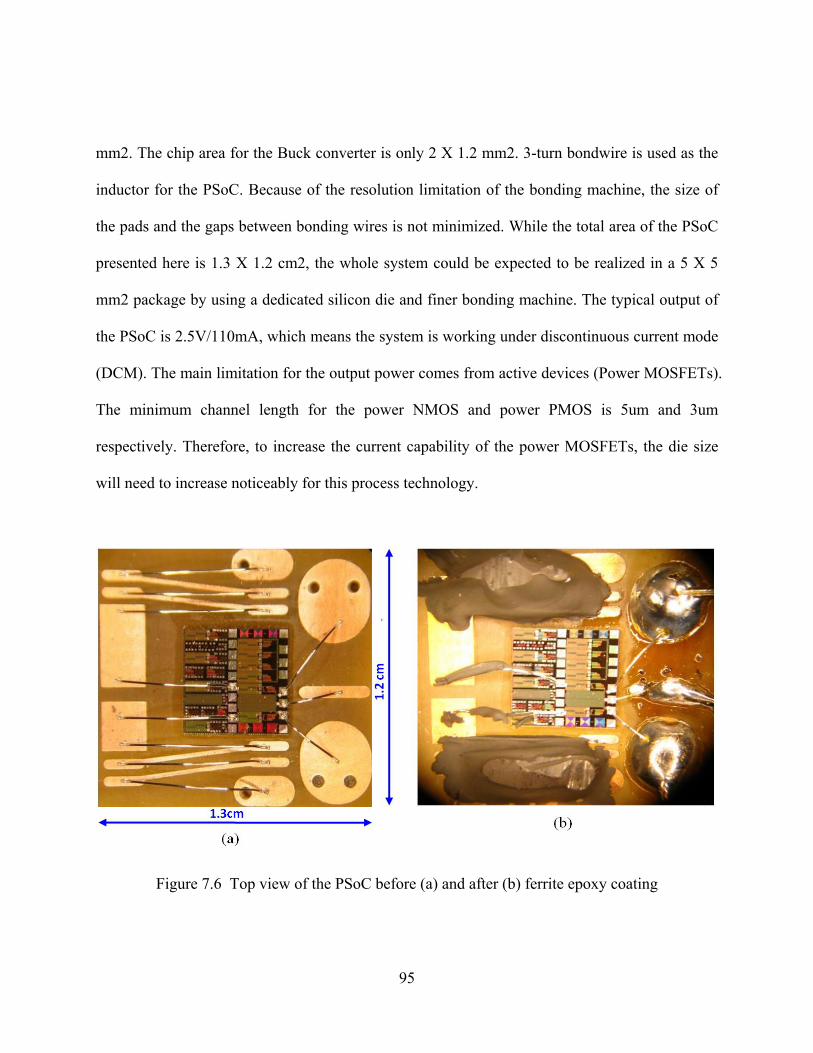
7.3 Package Design and Layout.......................................................................................... 94
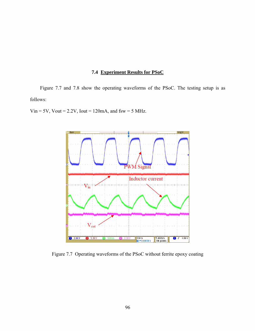
7.4 Experiment Results for PSoC ....................................................................................... 96
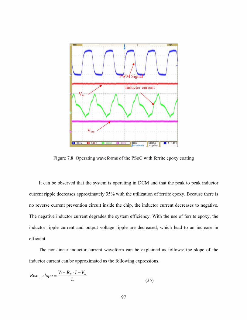
CHAPTER 8: CONCLUSION ................................................................................................... 100
REFERENCES ........................................................................................................................... 102
Page 10
ix
LIST OF FIGURES
Figure 1.1 PSoC Concept................................................................................................................ 2
Figure 1.2 Power SiP Product........................................................................................................ 4
Figure 1.3 Power SoC products ..................................................................................................... 5
Figure 1.4 PSiP and PSoC efficiency roadmap ............................................................................. 6
Figure 2.1 Die micrograph of doubly symmetric oscillator. [13] ................................................ 10
Figure 2.2 Scanning electron micrographs of a 7-turn square spiral inductor. [16] .................... 11
Figure 2.3 Measured and simulated Q of the 0.35-um 3.4-nH planar inductor. [23] .................. 11
Figure 2.4 Cross section of thin-film micro-inductor [24] .......................................................... 12
Figure 2.5 Top view of the fabricated micro-inductor[25] .......................................................... 13
Figure 2.6 Tyndall microinductor mounted on an 8-MHz commercially available buck converter
evaluation board[25] ............................................................................................................. 13
Figure 2.7 Quality factors of micro-inductors fabricated using standard IC fabrication
compatible process [25] ........................................................................................................ 14
Figure 2.8 Typical LTCC package............................................................................................... 17
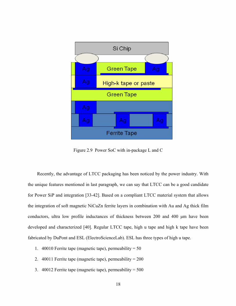
Figure 2.9 Power SoC with in-package L and C ......................................................................... 18
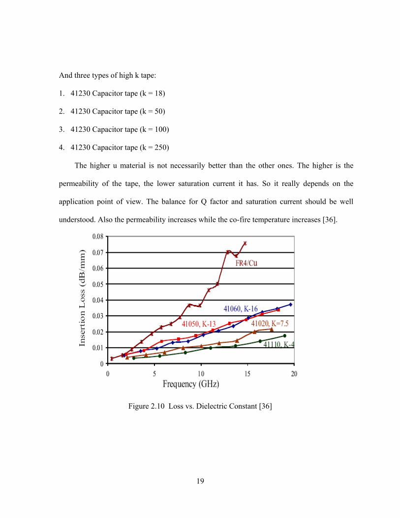
Figure 2.10 Loss vs. Dielectric Constant [36] ............................................................................. 19
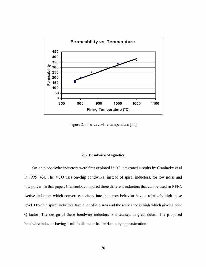
Figure 2.11 u vs co-fire temperature [36] .................................................................................... 20
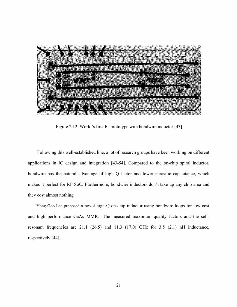
Figure 2.12 World’s first IC prototype with bondwire inductor [43] .......................................... 21
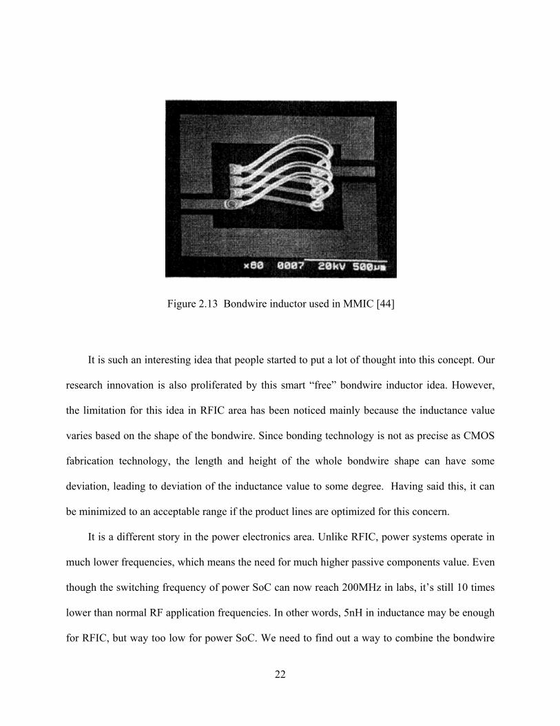
Figure 2.13 Bondwire inductor used in MMIC [44].................................................................... 22
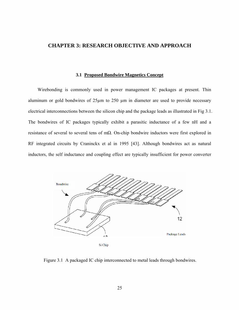
Figure 3.1 A packaged IC chip interconnected to metal leads through bondwires. .................... 25
Page 11
x
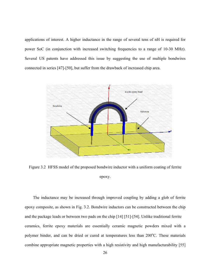
Figure 3.2 HFSS model of the proposed bondwire inductor with a uniform coating of ferrite
epoxy..................................................................................................................................... 26
Figure 3.3 Proposed method to increase bondwire inductance by using additional ferrite epoxy
beads. .................................................................................................................................... 27
Figure 3.4 Maxwell 3D processes................................................................................................ 29
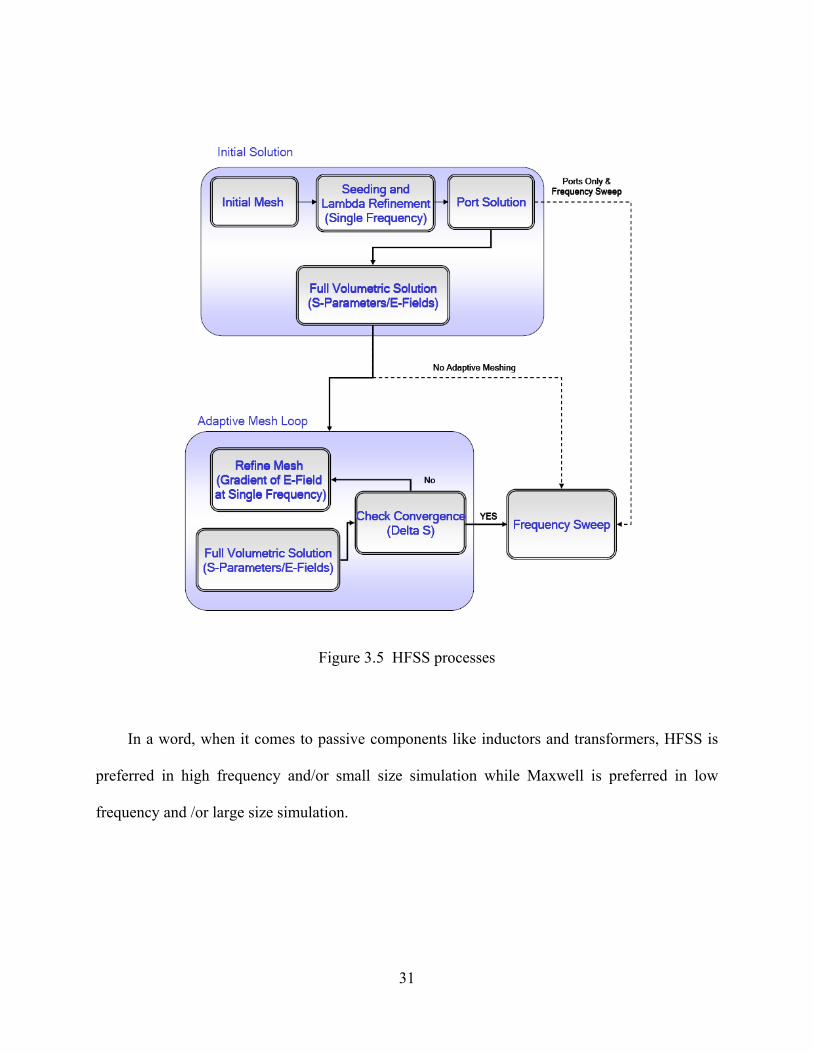
Figure 3.5 HFSS processes .......................................................................................................... 31
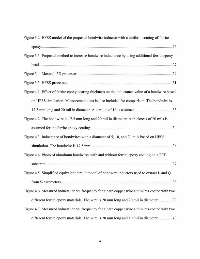
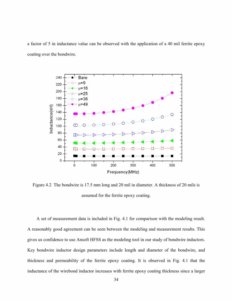
Figure 4.1 Effect of ferrite epoxy coating thickness on the inductance value of a bondwire based
on HFSS simulation. Measurement data is also included for comparison. The bondwire is
17.5 mm long and 20 mil in diameter. A µ value of 16 is assumed. .................................... 33
Figure 4.2 The bondwire is 17.5 mm long and 20 mil in diameter. A thickness of 20 mils is
assumed for the ferrite epoxy coating................................................................................... 34
Figure 4.3 Inductance of bondwires with a diameter of 5, 10, and 20 mils based on HFSS
simulation. The bondwire is 17.5 mm .................................................................................. 36
Figure 4.4 Photo of aluminum bondwires with and without ferrite epoxy coating on a PCB
substrate. ............................................................................................................................... 37
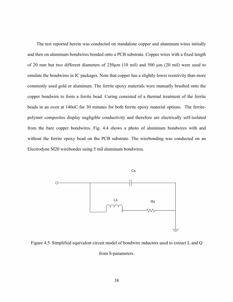
Figure 4.5 Simplified equivalent circuit model of bondwire inductors used to extract L and Q
from S-parameters................................................................................................................. 38
Figure 4.6 Measured inductance vs. frequency for a bare copper wire and wires coated with two
different ferrite epoxy materials. The wire is 20 mm long and 20 mil in diameter. ............. 39
Figure 4.7 Measured inductance vs. frequency for a bare copper wire and wires coated with two
different ferrite epoxy materials. The wire is 20 mm long and 10 mil in diameter. ............. 40
Page 12
xi
Figure 4.8 Comparison of the state-of-the-art MEMS micro-inductors, commercial wire wound
inductors, and the bondwire inductors .................................................................................. 41
Figure 4.9 Comparison of Q factors between the state-of-the-art MEMS micro-inductors,
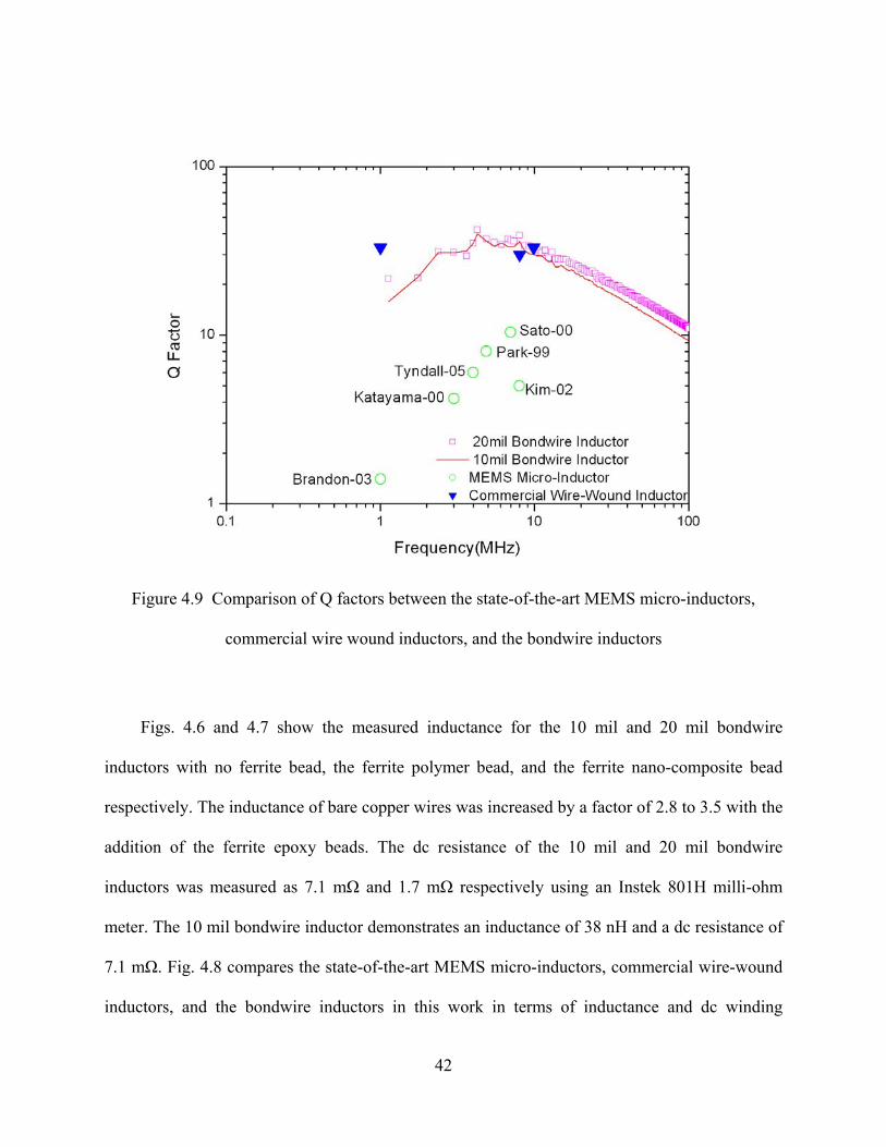
commercial wire wound inductors, and the bondwire inductors .......................................... 42
Figure 4.10 Measured high-frequency inductance for the 10 mil bondwire inductors with and
without ferrite beads. ............................................................................................................ 43
Figure 4.11 Measured switching waveform of the 10 mil bondwire inductors for core saturation
characterization ..................................................................................................................... 44
Figure 4.12 Concept of bondwire transformers. .......................................................................... 45
Figure 4.13 typical wirebond impedance from www.mosis.org.................................................. 45
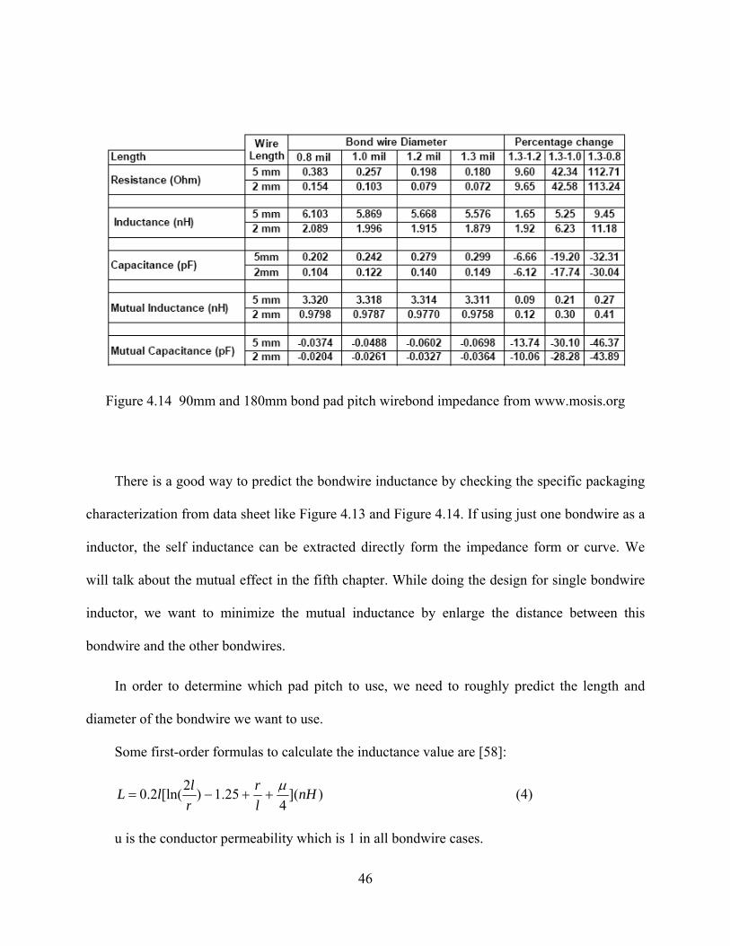
Figure 4.14 90mm and 180mm bond pad pitch wirebond impedance from www.mosis.org...... 46
Figure 4.15 HFSS simulation and empirical formula comparison .............................................. 48
Figure 5.1 The idea of multi-turn inductor vs single turn inductor ............................................. 51
Figure 5.2 Concept of coupled on-chip multi-turn (10-turn) bondwire inductor ........................ 53
Figure 5.3 HFSS simulation of multi-turn inductor without ferrite core...................................... 55
Figure 5.4 HFSS simulation of multi-turn inductor with ferrite core ........................................... 56
Figure 5.5 Empirical formula and hfss simulation comparison for self inductance .................... 58
Figure 5.6 Empirical formula and hfss simulation comparison for mutual inductance............... 60
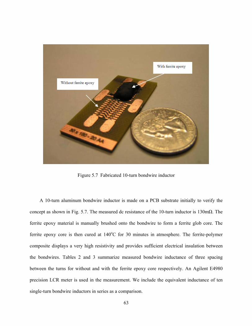
Figure 5.7 Fabricated 10-turn bondwire inductor ........................................................................ 63
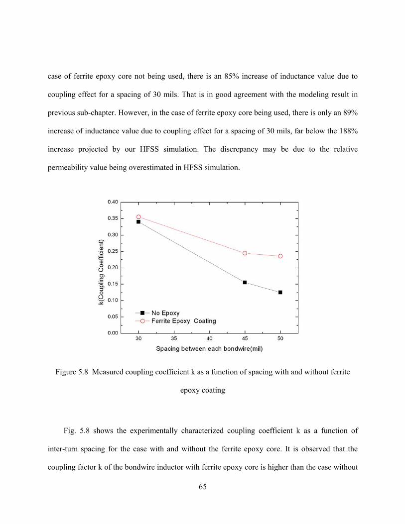
Figure 5.8 Measured coupling coefficient k as a function of spacing with and without ferrite
epoxy coating ........................................................................................................................ 65
Page 13
xii
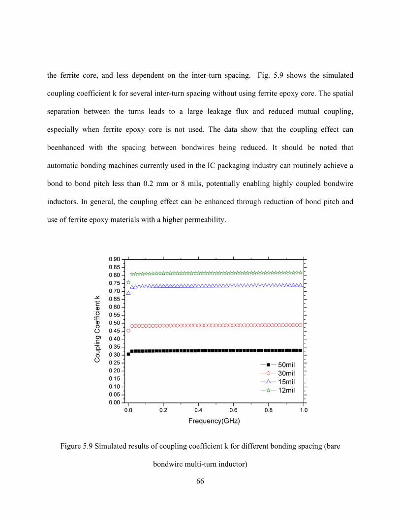
Figure 5.9 Simulated results of coupling coefficient k for different bonding spacing (bare
bondwire multi-turn inductor)............................................................................................... 66
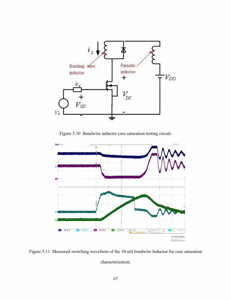
Figure 5.10 Bondwire inductor core saturation testing circuit. ................................................... 67
Figure 5.11 Measured switching waveform of the 10 mil bondwire Inductor for core saturation
characterization. .................................................................................................................... 67
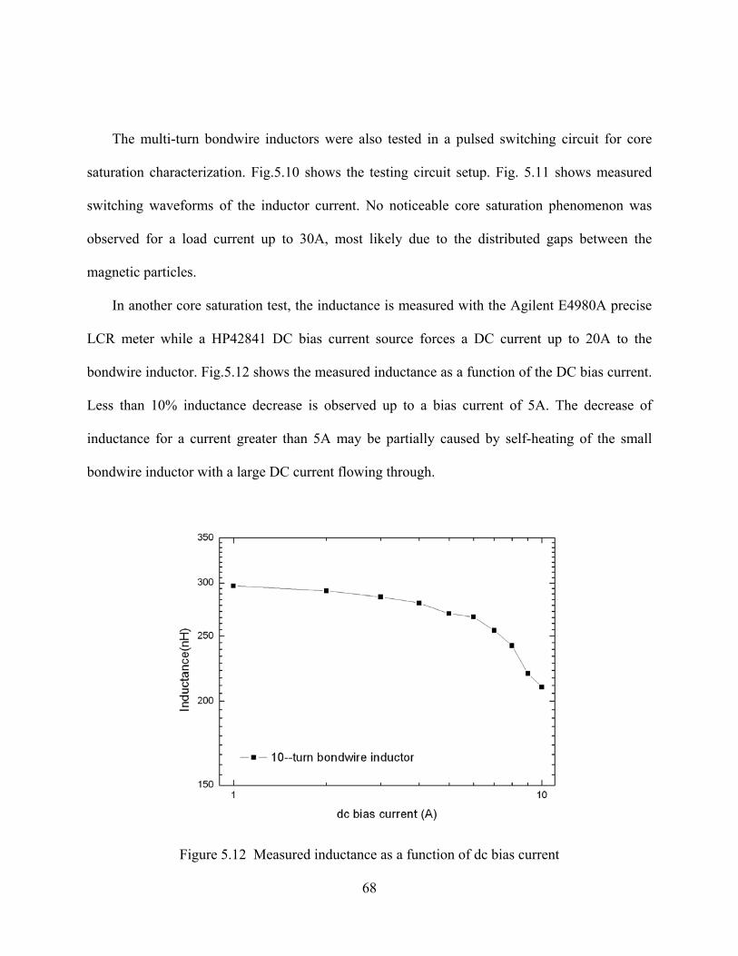
Figure 5.12 Measured inductance as a function of dc bias current.............................................. 68
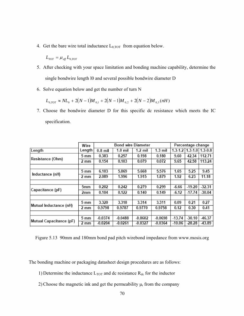
Figure 5.13 90mm and 180mm bond pad pitch wirebond impedance from www.mosis.org...... 70
Figure 6.1 Proposed on-chip transformer made of two or more sets of wirbonds sharing a ferrite
epoxy glob core on a chip ..................................................................................................... 72
Figure 6.2 Two-port transformer modeling with HFSS............................................................... 74
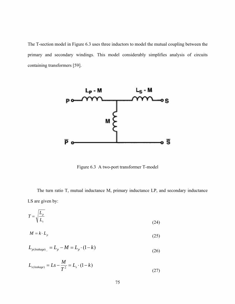
Figure 6.3 A two-port transformer T-model ................................................................................ 75
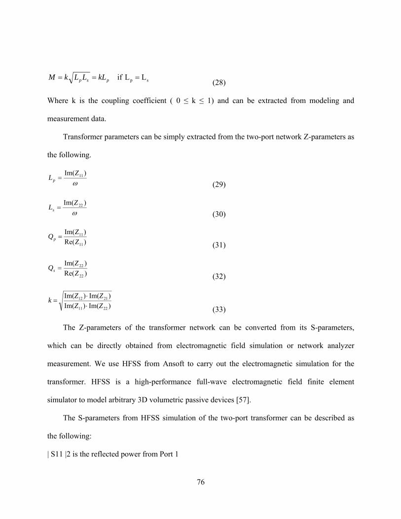
Figure 6.4 Simulated self inductance, mutual inductance and quality factor of a 15mil spacing
bondwire transformer............................................................................................................ 77
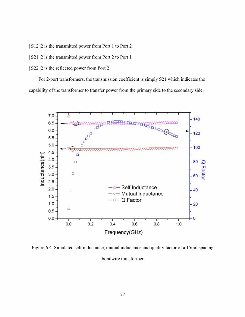
Figure 6.5 Coupling coefficient k for variable bonding spacing ................................................. 78
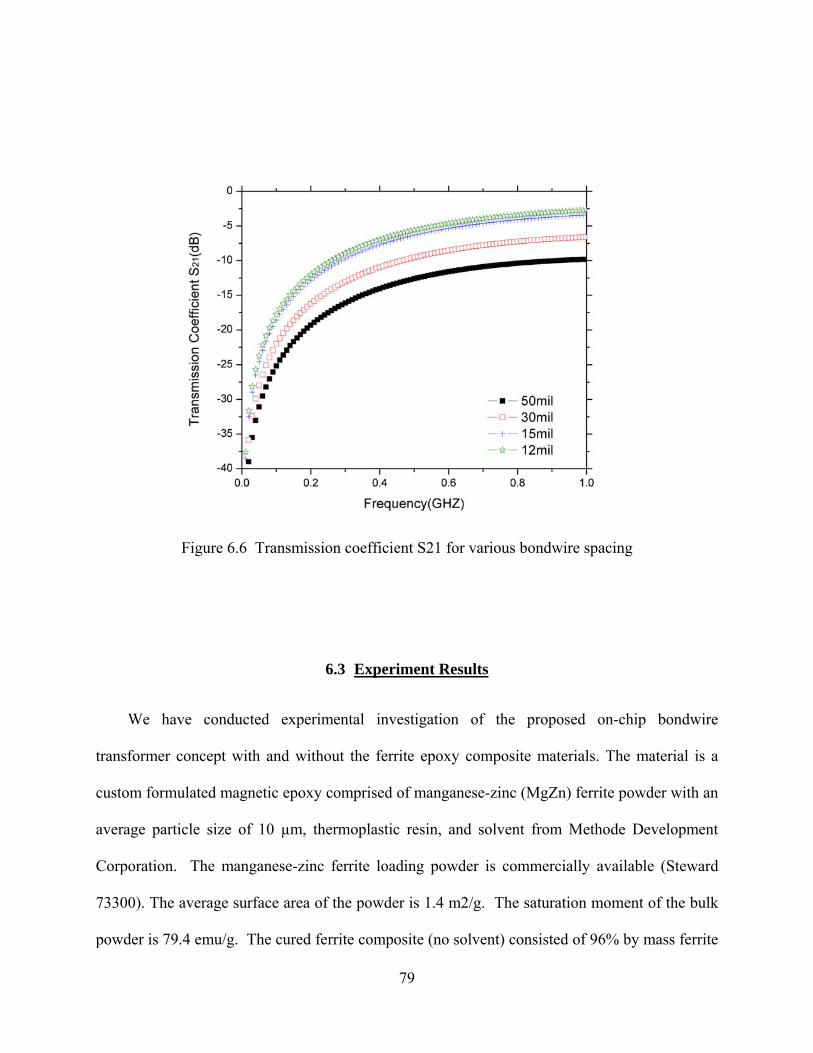
Figure 6.6 Transmission coefficient S21 for various bondwire spacing ..................................... 79
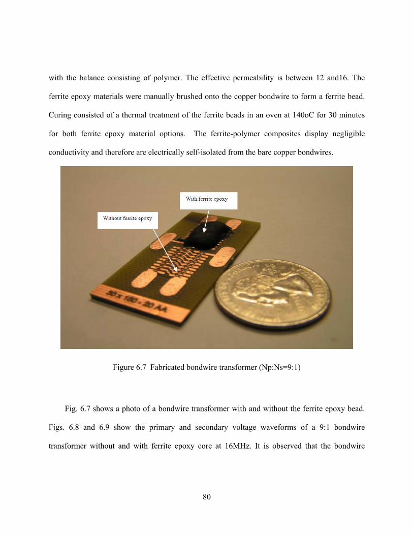
Figure 6.7 Fabricated bondwire transformer (Np:Ns=9:1) .......................................................... 80
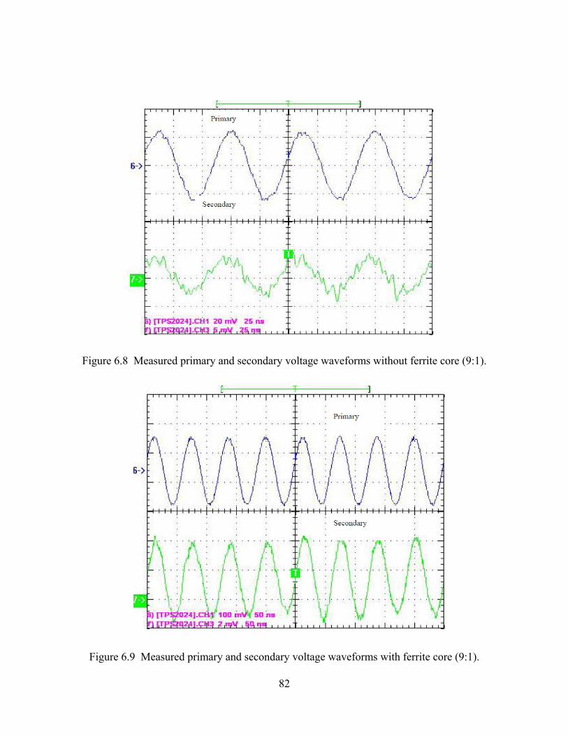
Figure 6.8 Measured primary and secondary voltage waveforms without ferrite core (9:1). ..... 82
Figure 6.9 Measured primary and secondary voltage waveforms with ferrite core (9:1)............ 82
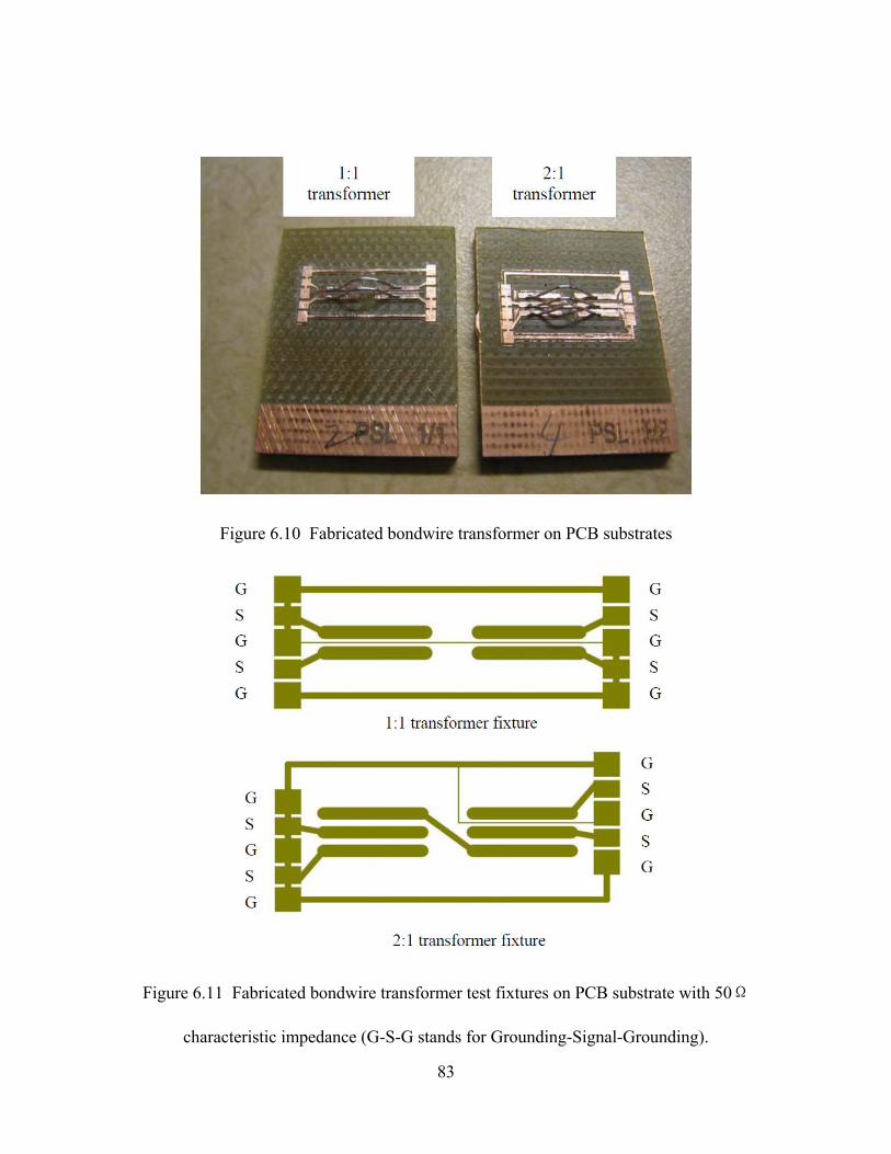
Figure 6.10 Fabricated bondwire transformer on PCB substrates ............................................... 83
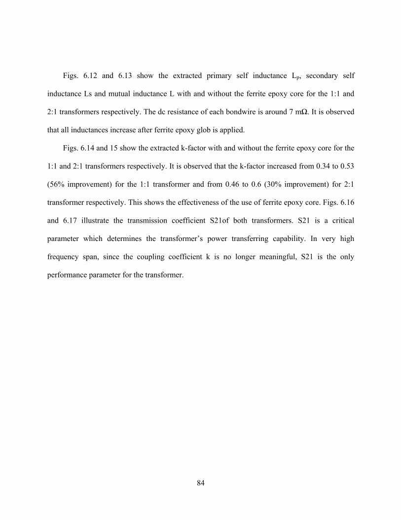
Figure 6.11 Fabricated bondwire transformer test fixtures on PCB substrate with
50Ωcharacteristic impedance (G-S-G stands for Grounding-Signal-Grounding). ............... 83
Page 14
xiii
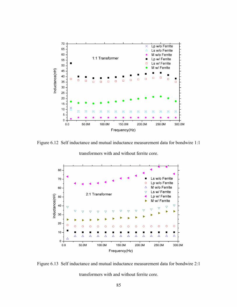
Figure 6.12 Self inductance and mutual inductance measurement data for bondwire 1:1
transformers with and without ferrite core............................................................................ 85
Figure 6.13 Self inductance and mutual inductance measurement data for bondwire 2:1
transformers with and without ferrite core............................................................................ 85
Figure 6.14 Measured transmission coefficient S21 of a 1:1 bondwire transformer before and
after applying ferrite epoxy................................................................................................... 86
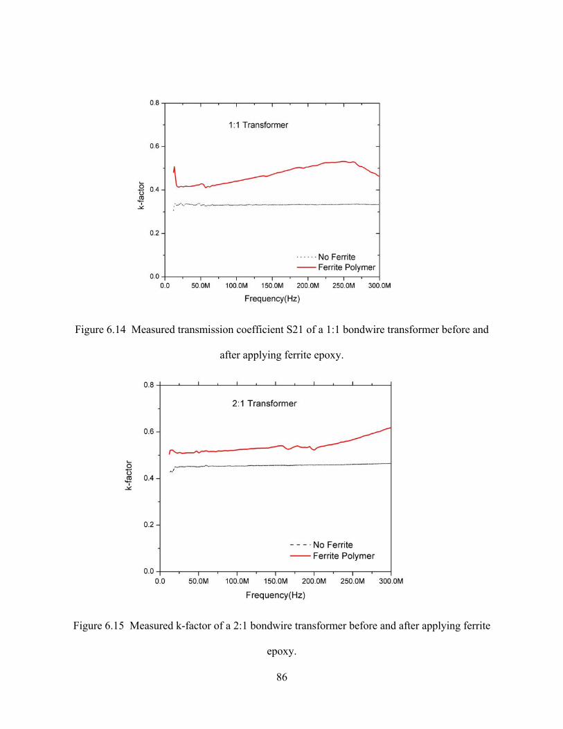
Figure 6.15 Measured k-factor of a 2:1 bondwire transformer before and after applying ferrite
epoxy..................................................................................................................................... 86
Figure 6.16 Measured k-factor of a 1:1 bondwire transformer before and after applying ferrite
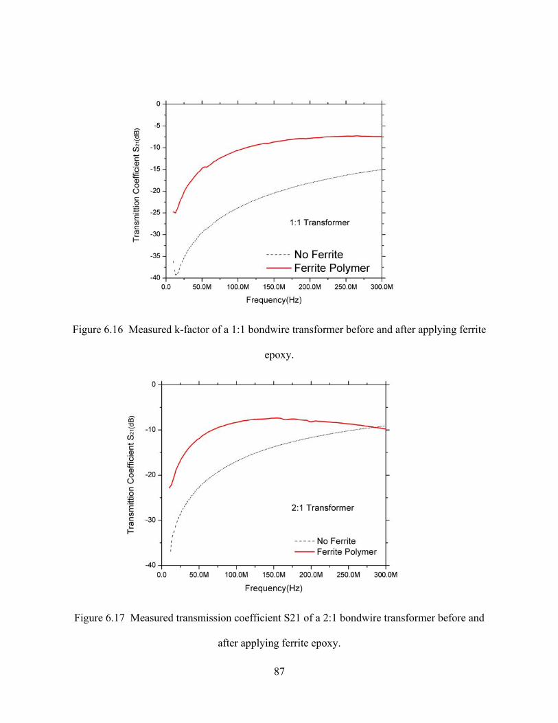
epoxy..................................................................................................................................... 87
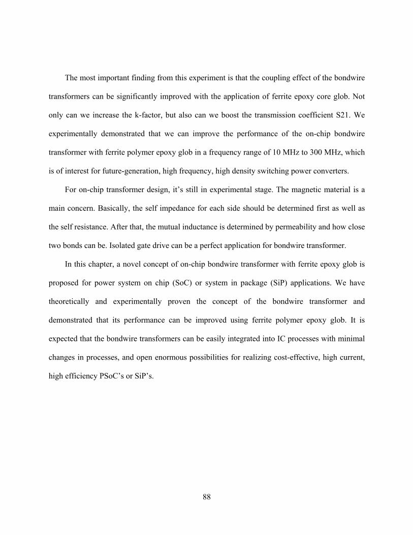
Figure 6.17 Measured transmission coefficient S21 of a 2:1 bondwire transformer before and
after applying ferrite epoxy................................................................................................... 87
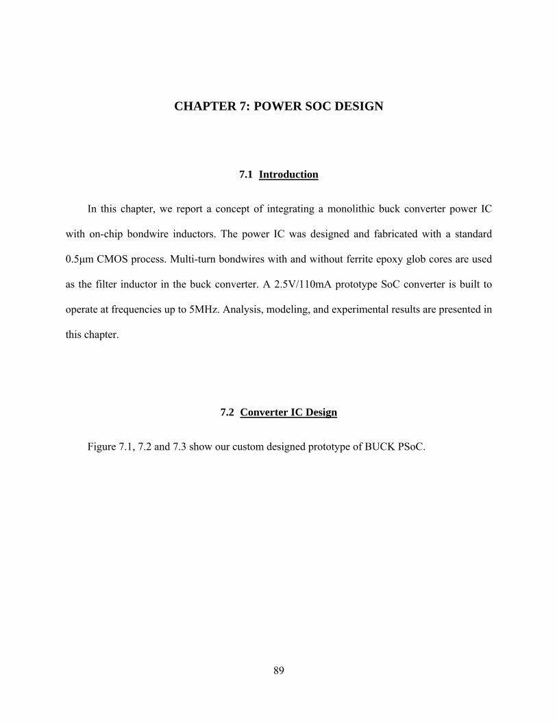
Figure 7.1 Schematic Diagram of Buck PSoC.............................................................................. 90
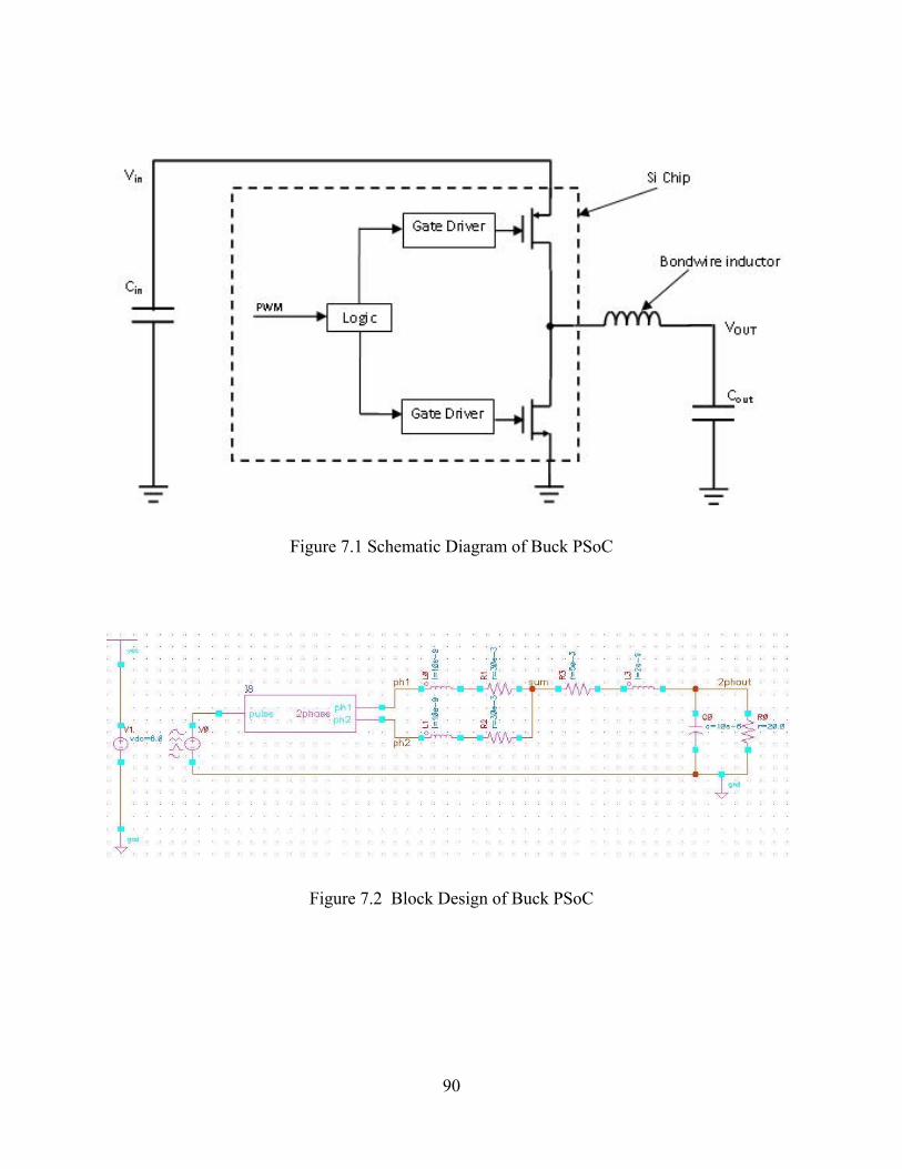
Figure 7.2 Block Design of Buck PSoC ...................................................................................... 90
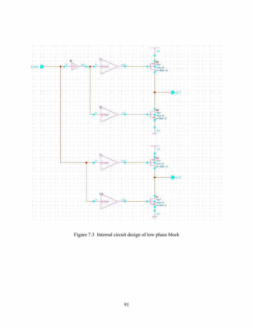
Figure 7.3 Internal circuit design of tow phase block.................................................................. 91
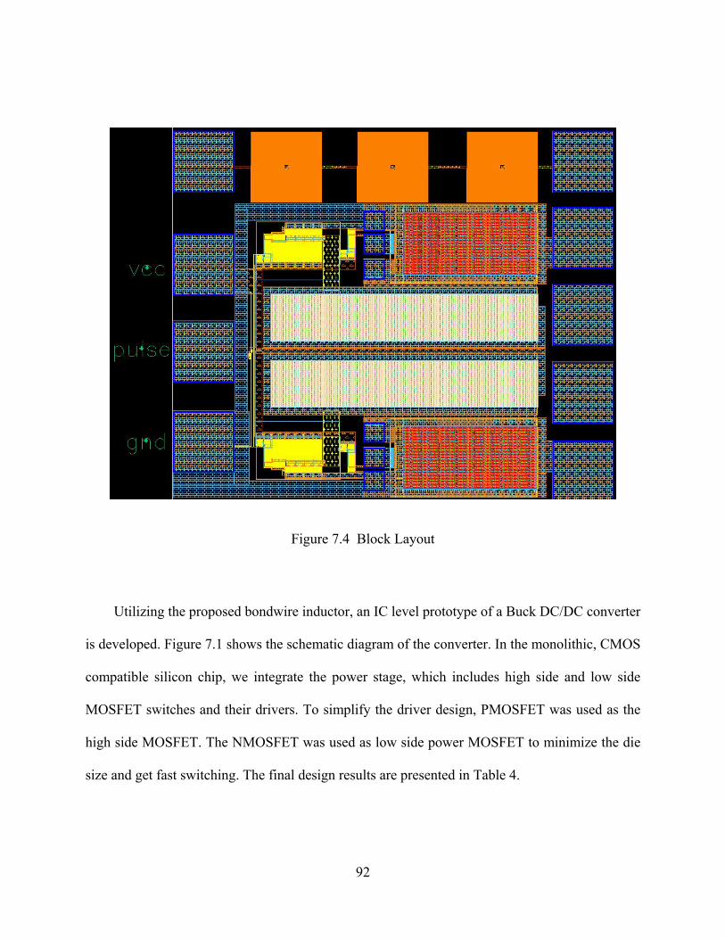
Figure 7.4 Block Layout .............................................................................................................. 92
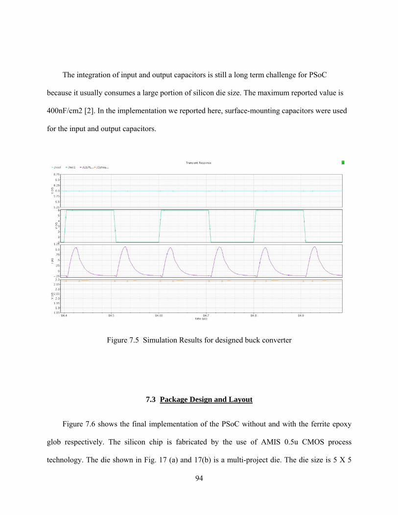
Figure 7.5 Simulation Results for designed buck converter ........................................................ 94
Figure 7.6 Top view of the PSoC before (a) and after (b) ferrite epoxy coating......................... 95
Figure 7.7 Operating waveforms of the PSoC without ferrite epoxy coating ............................. 96
Figure 7.8 Operating waveforms of the PSoC with ferrite epoxy coating................................... 97
Page 15
xiv
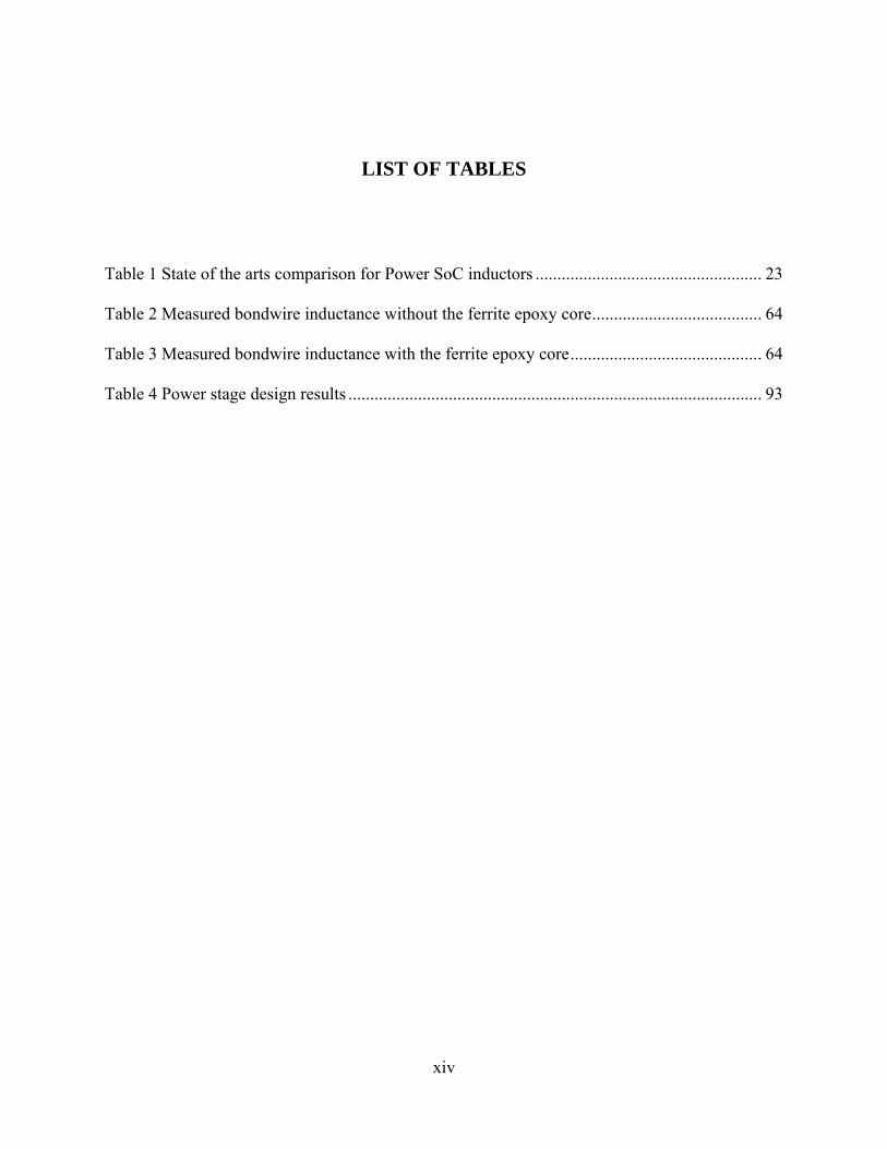
LIST OF TABLES
Table 1 State of the arts comparison for Power SoC inductors .................................................... 23
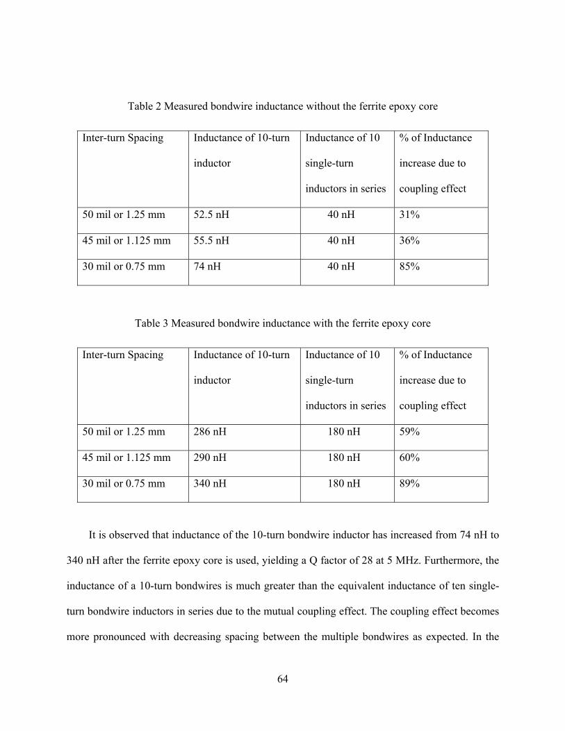
Table 2 Measured bondwire inductance without the ferrite epoxy core....................................... 64
Table 3 Measured bondwire inductance with the ferrite epoxy core............................................ 64
Table 4 Power stage design results ............................................................................................... 93
Page 16
xv
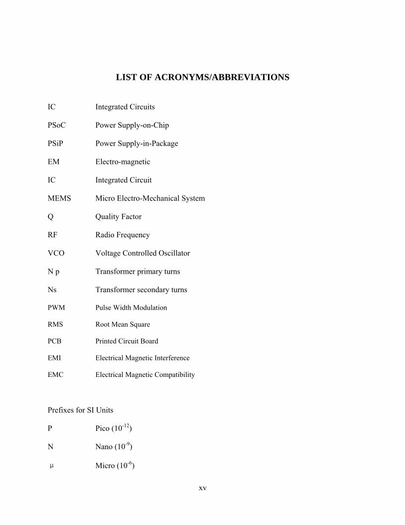
LIST OF ACRONYMS/ABBREVIATIONS
IC Integrated Circuits
PSoC Power Supply-on-Chip
PSiP Power Supply-in-Package
EM Electro-magnetic
IC Integrated Circuit
MEMS Micro Electro-Mechanical System
Q Quality Factor
RF Radio Frequency
VCO Voltage Controlled Oscillator
N p Transformer primary turns
Ns Transformer secondary turns
PWM Pulse Width Modulation
RMS Root Mean Square
PCB Printed Circuit Board
EMI Electrical Magnetic Interference
EMC Electrical Magnetic Compatibility
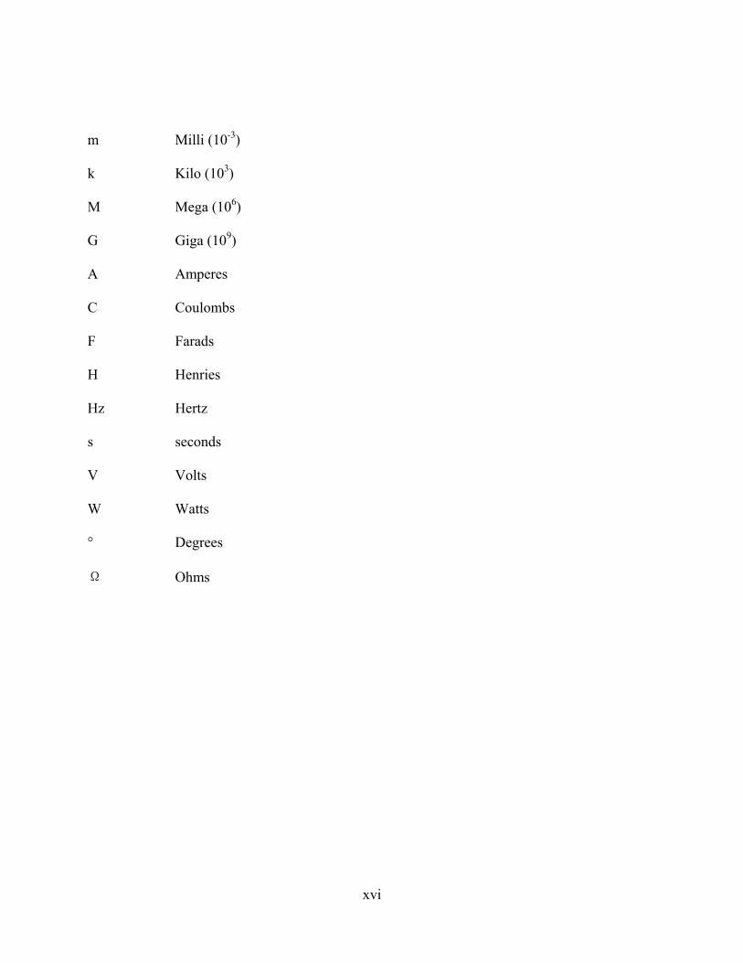
Prefixes for SI Units
P Pico (10-12)
N Nano (10-9)
μ Micro (10-6)
Page 17
xvi
m Milli (10-3)
k Kilo (103)
M Mega (106)
G Giga (109)
A Amperes
C Coulombs
F Farads
H Henries
Hz Hertz
s seconds
V Volts
W Watts
° Degrees
Ω Ohms
Page 18
1
CHAPTER 1: INTRODUCTION
1.1 Power SoC & SiP Motivation
Power supplies are converters that translate the electrical power from one end to another
end. All electrical equipment need power supplies so that they can serve everywhere in our
everyday life. Ac-dc power supplies can translate 110V(US) or 220V(China) ac power to IC
power or to another distribution power such as 12V(PC). A Dc-dc converter can convert 12V to
3.3V for IC usage. A report from Gartner Group said that power management devices represent
44% of the whole $ 16.4 billion Analog IC market. In the year 2007, the dc-dc converter market
was $1.5 billion. Gartner also projects the market will increased to $ 2.5 billion in 2011 [1].
System on Chip (SoC) is an emerging trend of integrating all components of an electronic
system including digital, analog, mixed-signal, communications and sensor functions into a
single integrated circuit. The SoC concept embodies what many believe to be the ultimate level
of integration: an entire system on one chip. Since its emergence in the 1990’s, the SoC concept
has gained wide acceptance in a broad range of applications from supercomputing to embedded
systems. The proliferation of the SoC concept into power management systems has also
generated a great deal of interest in the electronics industry. Power management is a key
enabling technology behind the digital revolution. Each year hundreds of millions of power
converters are manufactured and embedded into computers, telecommunication equipment,
consumer products, automobiles, and industrial control systems worldwide. Powering various
ICs such as microprocessors, ASICs and FPGAs, these dc-dc non-isolated power supplies are
Page 19
2
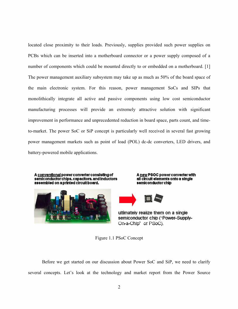
located close proximity to their loads. Previously, supplies provided such power supplies on
PCBs which can be inserted into a motherboard connector or a power supply composed of a
number of components which could be mounted directly to or embedded on a motherboard. [1]
The power management auxiliary subsystem may take up as much as 50% of the board space of
the main electronic system. For this reason, power management SoCs and SIPs that
monolithically integrate all active and passive components using low cost semiconductor
manufacturing processes will provide an extremely attractive solution with significant
improvement in performance and unprecedented reduction in board space, parts count, and time-
to-market. The power SoC or SiP concept is particularly well received in several fast growing
power management markets such as point of load (POL) dc-dc converters, LED drivers, and
battery-powered mobile applications.
Figure 1.1 PSoC Concept
Before we get started on our discussion about Power SoC and SiP, we need to clarify
several concepts. Let’s look at the technology and market report from the Power Source
Page 20
3
Manufacturing Association for definitions. Power SoC (Power-supply-on-chip) is a
semiconductor or chip integrated version where the product has components on one or two
semiconductor substrates. Power SiP (Power-supply-in-package) is a package integrated version
that contains a couple of components, with the semiconductor content integrated onto a single
chip to various degrees by the supplier.
Considering the slight and confusing definition difference between them and the difficulties
to integrate passive components such as capacitors and inductors on both of them, it is hard to
draw a border line between them. The fact that Power SOC and SIP are serving almost the same
market makes them even harder to identify. They look more like twins who compete and
complement each other at the same time. In my opinion, it doesn’t matter whose name is whose.
The integration concept and implementation is the key to achieve further power supply
evolvement.
Page 21
4
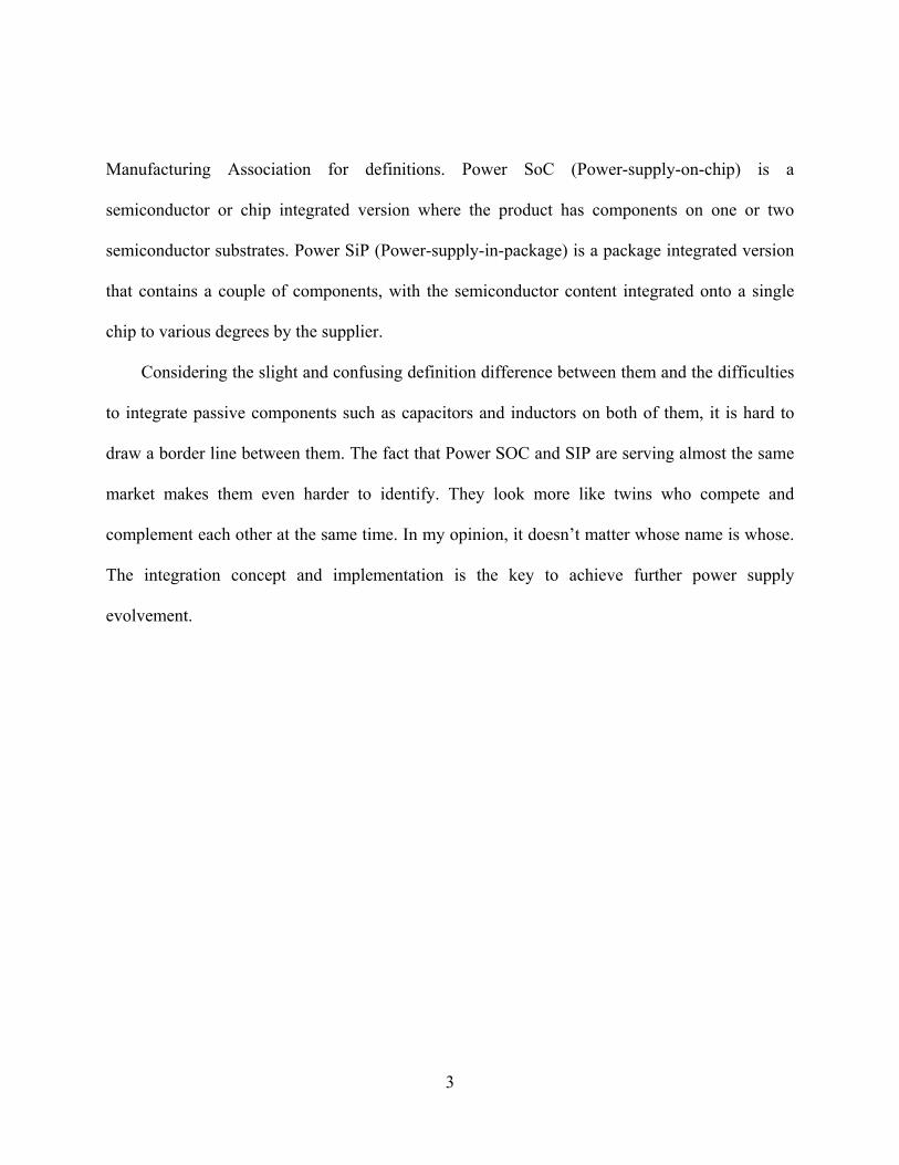
Figure 1.2 Power SiP Product
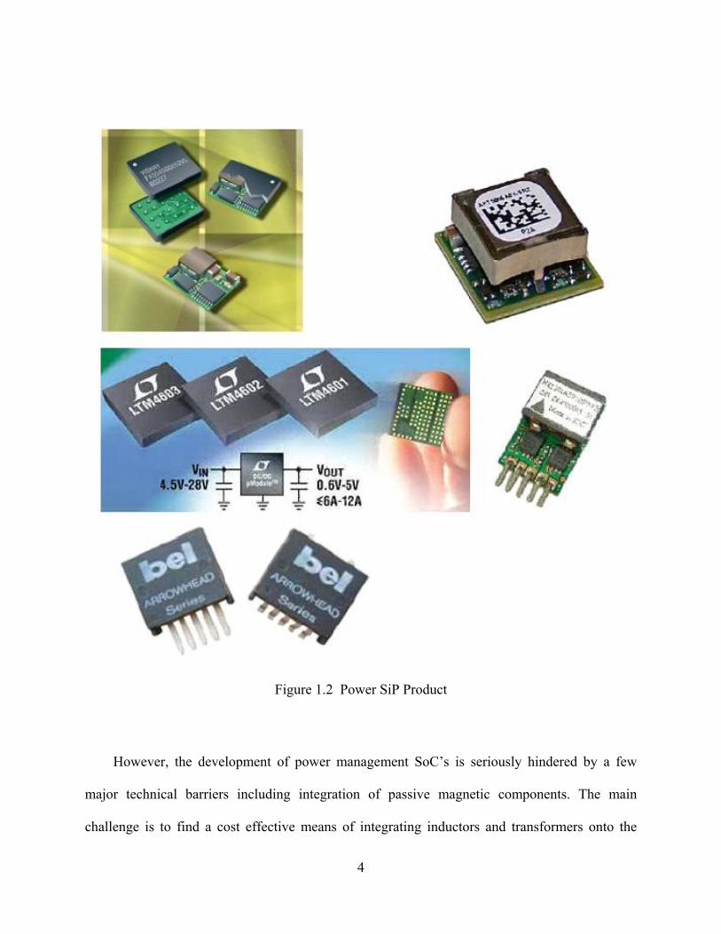
However, the development of power management SoC’s is seriously hindered by a few
major technical barriers including integration of passive magnetic components. The main
challenge is to find a cost effective means of integrating inductors and transformers onto the
Page 22
5
silicon chip, while achieving adequate performance in terms of inductance, dc & ac series
resistance, maximum saturation current, magnetic coupling coefficient and Q factor. Current
research work on integrated magnetics for power SoC’s has predominantly focused on utilizing
MEMS (micro- electro-mechanical-system) micromachining technology as a post-processing
Figure 1.3 Power SoC products
Page 23
6
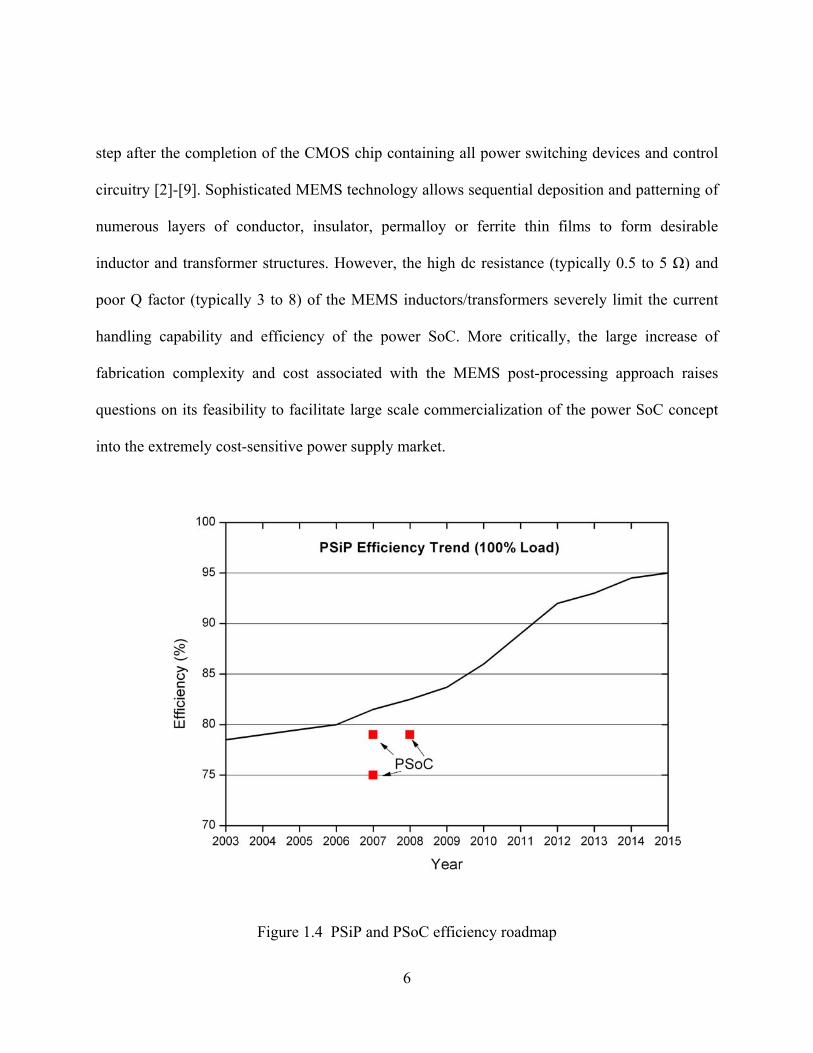
step after the completion of the CMOS chip containing all power switching devices and control
circuitry [2]-[9]. Sophisticated MEMS technology allows sequential deposition and patterning of
numerous layers of conductor, insulator, permalloy or ferrite thin films to form desirable
inductor and transformer structures. However, the high dc resistance (typically 0.5 to 5 Ω) and
poor Q factor (typically 3 to 8) of the MEMS inductors/transformers severely limit the current
handling capability and efficiency of the power SoC. More critically, the large increase of
fabrication complexity and cost associated with the MEMS post-processing approach raises
questions on its feasibility to facilitate large scale commercialization of the power SoC concept
into the extremely cost-sensitive power supply market.
Figure 1.4 PSiP and PSoC efficiency roadmap
Page 24
7
In this work, we propose and investigate a new cost-effective approach to form on-chip
inductors utilizing existing bondwires with additional ferrite epoxy beads formed during the
packaging process. For convenience and consistence with our other published papers, we classify
this kind of power supply system with bondwire inductors and transformers as PSoC in this work.
1.2 Organization of This Thesis
As studied in the previous section, a high performance on-chip or in-package power circuit
magnetic device design method is in high demand for both academic study and industrial
development.
This dissertation is constructed with eight chapters. The first chapter introduces the
importance of Power SoC and SiP implementation and describes the aim of this dissertation. The
second chapter reviews a significant amount of the most updated literatures related to the topic,
including on-chip inductor, MEMS inductor, PCB & LTCC package magnetics and bondwire RF
inductors, and offers a clear clue about on-chip inductor physics and modeling. Chapter three
explores the unknown area of bondwire magnetics for power IC and the finite element modeling
tools, Ansoft HFSS and Maxwell 3D, are introduced and discussed. Chapter four covers our
newly proposed bondwire inductor with ferrite epoxy, and proposes a compact and effective
model structure to address this discovery. Modeling and experiment of multi-turn inductors
utilizing the so called coupling effect is presented in chapter 5. Chapter six proposes a brand new
concept about bondwire transformer with accurate modeling and testing. Chapter seven further
Page 25
8
elaborates on the proposed power SoC concept by building the prototype of dc-dc buck converter
IC as well as the whole package. IC and the whole function block is measured and presented in
this chapter. And lastly, chapter eight concludes the whole dissertation, and leads to future work.
Page 26
9
CHAPTER 2: STATE OF THE ARTS
In this chapter, integration of passive components such as inductors, capacitors and
transformers is discussed by order of different implementation methods as previous art. Both the
advantages and disadvantages are concluded in each sub-chapter.
2.1 CMOS On-Chip Magnetics
On-chip inductors have been a very important research area since early the 1990’s when it
was first presented. A lot of work has been done and reported in literature [13]-[23]. Some of the
methods have been used in industry, but not released to college and institution yet [22]. A
comprehensive solution and library for Cadence have been already developed by TSMC. The on-chip
spiral inductor library is completed based on accurate one by one measurement results by this
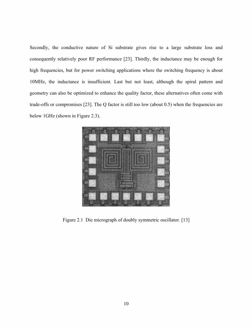
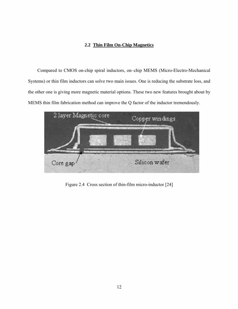
foundry. A typical Oscillator die with an on-chip inductor is shown in Figure 2.1 and a SEM
image of a 7-turn spiral inductor is shown in Figure 2.2
The first planar inductor on silicon was developed by Nguyen and Meyer in 1990 [19] using
the interconnect technology, and a simple π model was proposed by them to describe the
inductor’s behavior in that paper as well. Thereafter, people started to improve the model like
Ashby et al. [20], Yue and Wong [21].
Although TSMC did a great job extracting all of the parameters for Cadence library and the
library itself is very convenient and accurate for RFIC design, the fact of natural shortage of on-
chip spiral inductor still remains. First of all, the inductor takes up a lot of the chip area (Fig. 2.1).
Page 27
10
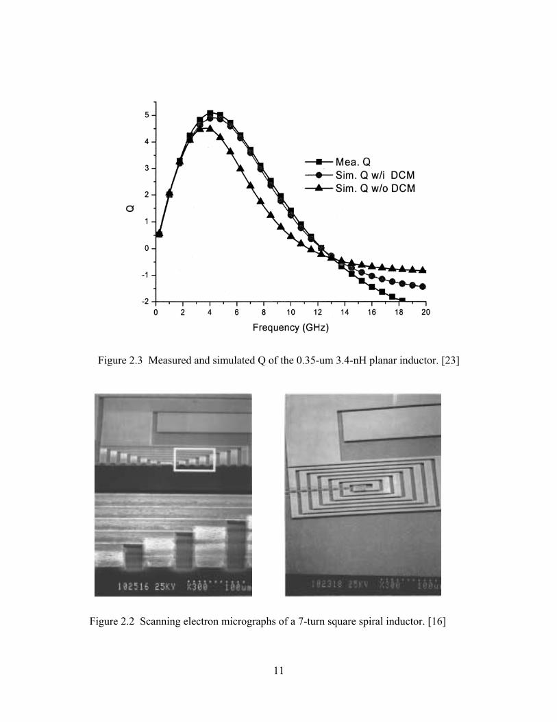
Secondly, the conductive nature of Si substrate gives rise to a large substrate loss and
consequently relatively poor RF performance [23]. Thirdly, the inductance may be enough for
high frequencies, but for power switching applications where the switching frequency is about
10MHz, the inductance is insufficient. Last but not least, although the spiral pattern and
geometry can also be optimized to enhance the quality factor, these alternatives often come with
trade-offs or compromises [23]. The Q factor is still too low (about 0.5) when the frequencies are
below 1GHz (shown in Figure 2.3).
Figure 2.1 Die micrograph of doubly symmetric oscillator. [13]
Page 28
11
Figure 2.3 Measured and simulated Q of the 0.35-um 3.4-nH planar inductor. [23]
Figure 2.2 Scanning electron micrographs of a 7-turn square spiral inductor. [16]
Page 29
12
2.2 Thin Film On-Chip Magnetics
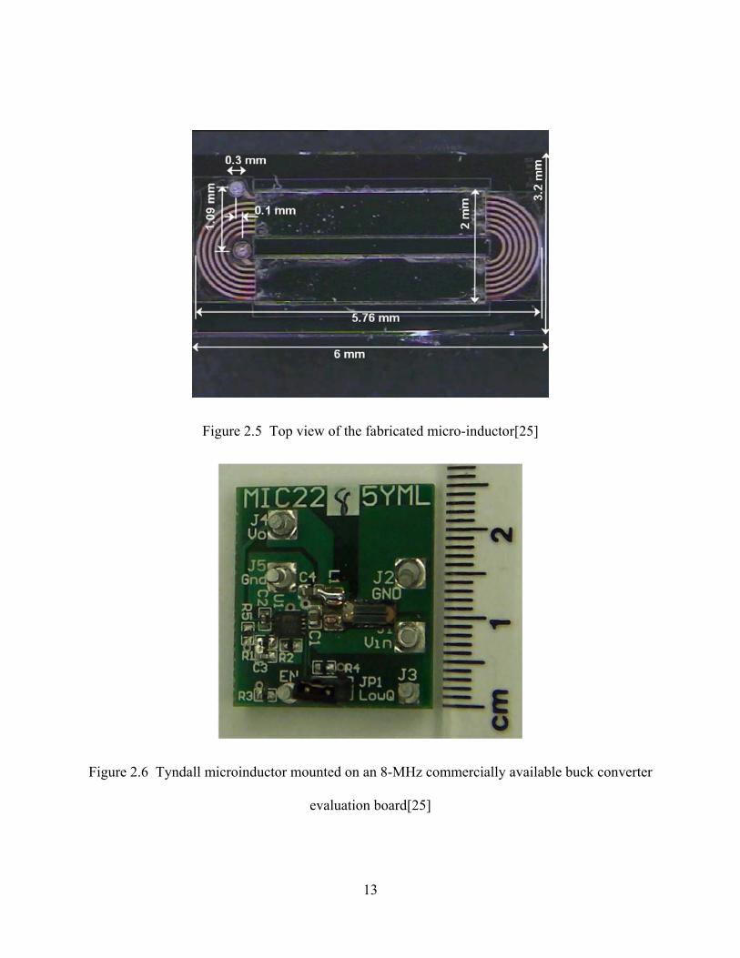
Compared to CMOS on-chip spiral inductors, on–chip MEMS (Micro-Electro-Mechanical
Systems) or thin film inductors can solve two main issues. One is reducing the substrate loss, and
the other one is giving more magnetic material options. These two new features brought about by
MEMS thin film fabrication method can improve the Q factor of the inductor tremendously.
Figure 2.4 Cross section of thin-film micro-inductor [24]
Page 30
13
Figure 2.5 Top view of the fabricated micro-inductor[25]
Figure 2.6 Tyndall microinductor mounted on an 8-MHz commercially available buck converter
evaluation board[25]
Page 31
14
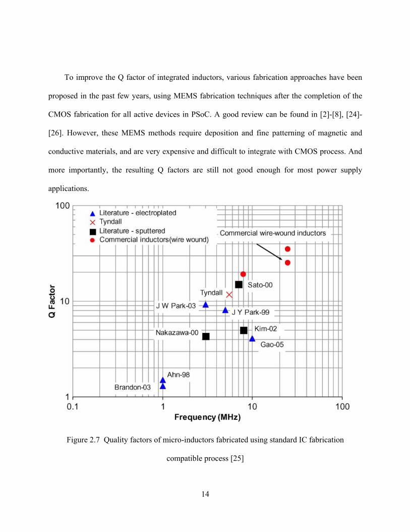
To improve the Q factor of integrated inductors, various fabrication approaches have been
proposed in the past few years, using MEMS fabrication techniques after the completion of the
CMOS fabrication for all active devices in PSoC. A good review can be found in [2]-[8], [24]-
[26]. However, these MEMS methods require deposition and fine patterning of magnetic and
conductive materials, and are very expensive and difficult to integrate with CMOS process. And
more importantly, the resulting Q factors are still not good enough for most power supply
applications.
Figure 2.7 Quality factors of micro-inductors fabricated using standard IC fabrication
compatible process [25]
Page 32
15
Sputter deposited magnetic materials can generally have high resistivity, which results in
low core eddy current loss and a relatively high Q factor of the micro-inductor [2]-[9]. High
resistivity and high saturation magnetic materials are the key to achieve low loss components by
suppressing the eddy current [10][11]. The other way to solve this eddy current loss problem is
lamination. Most of the lamination reported so far in the literature is done with physical vapor
deposition (PVD) techniques. However, Physical Vapor Deposition techniques present several
drawbacks such as the depositing rate being relatively slow, so that production of layers more
than a couple of microns thick becomes quite expensive [26]. Tyndall used almost entirely
aqueous-based electrochemical processes to deposit magnetic materials [25], which is a
relatively cost efficient way to deposit thin films. With a self resonant frequency of 130 MHz,
the inductance at low frequency is approximately 440 nH with a dc resistance of 0.5 ohms, and a
high quality factor of 11.7 at 5.5 MHz. The current handling capability test shows less than 10%
decrease in inductance at 500-mA current [25].
2.3 PCB Magnetics
PCBs (Printed Circuit Boards) are widely used in almost all the power supplies as a
substrate. Scientists and engineers around the world did a lot of research on integration of
inductors and transformers try to take advantage of the well-established PCB product lines [27]-
[32]. However, when the inductors are built on PCB substrate, they will be compared to the
discrete commercial inductors for performance since no one cares too much about the space here.
Page 33
16
Compared to discrete inductor with high-u magnetic core, the PCB inductor by nature has lower
inductance thus lower Q factors. Although it’s true that this shortness can be compensated by
insertion of magnetic layer inside, the extra cost can be noticeable. Plus, the relative larger size
inductors have low self resonate frequencies due to the relatively larger parasitic capacitance.
Matthias Ludwig reported in [22] that, in an area of 10mmx10mm of a six-layer PCB, the
inductance with magnetic plate can be as high as 4.7uH/500mA at 1MHz. In contrast, a typical
commercial 4.7uH/1.5A inductor only has a dimension of 2.66mm x 2.41mm x 2.16mm.
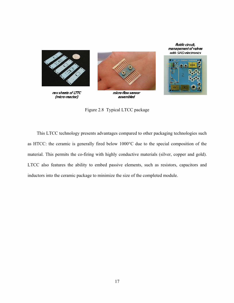
2.4 LTCC Magnetics
LTCC (Low Temperature Co-fired Ceramic) is a mature multi-layer technology that has
been used for many years in the microelectronics packaging industry. Each of the layers are
processed in parallel and only brought together in an accurately aligned stack immediately prior
to firing. This is the key differentiator to serially produced multi-layer structures such as thick
film hybrid interconnect and components such as ceramic capacitors. LTCC technology is
especially beneficial for RF and high-frequency applications. In RF and wireless applications,
LTCC technology is also used to produce multilayer hybrid integrated circuits, which can
include resistors, inductors, capacitors, and active components in the same package. LTCC
hybrids have a smaller initial ("non recurring") cost as compared with ICs, making them an
attractive alternative to ASICs for small scale integration devices.
Page 34
17
Figure 2.8 Typical LTCC package
This LTCC technology presents advantages compared to other packaging technologies such
as HTCC: the ceramic is generally fired below 1000°C due to the special composition of the
material. This permits the co-firing with highly conductive materials (silver, copper and gold).
LTCC also features the ability to embed passive elements, such as resistors, capacitors and
inductors into the ceramic package to minimize the size of the completed module.
Page 35
18
Figure 2.9 Power SoC with in-package L and C
Recently, the advantage of LTCC packaging has been noticed by the power industry. With
the unique features mentioned in last paragraph, we can say that LTCC can be a good candidate
for Power SiP and integration [33-42]. Based on a compliant LTCC material system that allows
the integration of soft magnetic NiCuZn ferrite layers in combination with Au and Ag thick film
conductors, ultra low profile inductances of thickness between 200 and 400 μm have been
developed and characterized [40]. Regular LTCC tape, high u tape and high k tape have been
fabricated by DuPont and ESL (ElectroScienceLab). ESL has three types of high u tape.
1. 40010 Ferrite tape (magnetic tape), permeability = 50
2. 40011 Ferrite tape (magnetic tape), permeability = 200
3. 40012 Ferrite tape (magnetic tape), permeability = 500
Page 36
19
And three types of high k tape:
1. 41230 Capacitor tape (k = 18)
2. 41230 Capacitor tape (k = 50)
3. 41230 Capacitor tape (k = 100)
4. 41230 Capacitor tape (k = 250)
The higher u material is not necessarily better than the other ones. The higher is the
permeability of the tape, the lower saturation current it has. So it really depends on the
application point of view. The balance for Q factor and saturation current should be well
understood. Also the permeability increases while the co-fire temperature increases [36].
Figure 2.10 Loss vs. Dielectric Constant [36]
Page 37
20
Figure 2.11 u vs co-fire temperature [36]
2.5 Bondwire Magnetics
On-chip bondwire inductors were first explored in RF integrated circuits by Craninckx et al
in 1995 [43]. The VCO uses on-chip bondwires, instead of spiral inductors, for low noise and
low power. In that paper, Craninckx compared three different inductors that can be used in RFIC.
Active inductors which convert capacitors into inductors behavior have a relatively high noise
level. On-chip spiral inductors take a lot of die area and the resistance is high which gives a poor
Q factor. The design of these bondwire inductors is discussed in great detail. The proposed
bondwire inductor having 1 mil in diameter has 1nH/mm by approximation.
Page 38
21
Following this well-established line, a lot of research groups have been working on different
applications in IC design and integration [43-54]. Compared to the on-chip spiral inductor,
bondwire has the natural advantage of high Q factor and lower parasitic capacitance, which
makes it perfect for RF SoC. Furthermore, bondwire inductors don’t take up any chip area and
they cost almost nothing.
Yong-Goo Lee proposed a novel high-Q on-chip inductor using bondwire loops for low cost
and high performance GaAs MMIC. The measured maximum quality factors and the self-
resonant frequencies are 21.1 (26.5) and 11.3 (17.0) GHz for 3.5 (2.1) nH inductance,
respectively [44].
Figure 2.12 World’s first IC prototype with bondwire inductor [43]
Page 39
22
It is such an interesting idea that people started to put a lot of thought into this concept. Our
research innovation is also proliferated by this smart “free” bondwire inductor idea. However,
the limitation for this idea in RFIC area has been noticed mainly because the inductance value
varies based on the shape of the bondwire. Since bonding technology is not as precise as CMOS
fabrication technology, the length and height of the whole bondwire shape can have some
deviation, leading to deviation of the inductance value to some degree. Having said this, it can
be minimized to an acceptable range if the product lines are optimized for this concern.
It is a different story in the power electronics area. Unlike RFIC, power systems operate in
much lower frequencies, which means the need for much higher passive components value. Even
though the switching frequency of power SoC can now reach 200MHz in labs, it’s still 10 times
lower than normal RF application frequencies. In other words, 5nH in inductance may be enough
for RFIC, but way too low for power SoC. We need to find out a way to combine the bondwire
Figure 2.13 Bondwire inductor used in MMIC [44]
Page 40
23
inductor idea with our specific Power SoC application. The details will be presented in the
following chapters.
2.6 Discussions
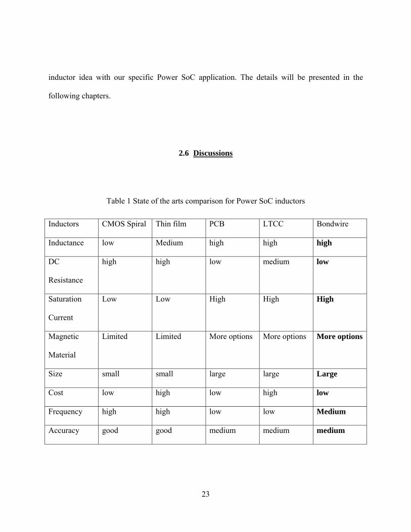
Table 1 State of the arts comparison for Power SoC inductors
Inductors CMOS Spiral Thin film PCB LTCC Bondwire
Inductance low Medium high high high
DC
Resistance
high high low medium low
Saturation
Current
Low Low High High High
Magnetic
Material
Limited Limited More options More options More options
Size small small large large Large
Cost low high low high low
Frequency high high low low Medium
Accuracy good good medium medium medium
Page 41
24
This form shows the comparison between the current hot research area for Power SoC
inductors and transformers. Bondwire inductors and transformers by nature are very promising
candidates. The design and fabrication details will be discussed in the next chapters.
Page 42
25
CHAPTER 3: RESEARCH OBJECTIVE AND APPROACH
3.1 Proposed Bondwire Magnetics Concept
Wirebonding is commonly used in power management IC packages at present. Thin
aluminum or gold bondwires of 25µm to 250 µm in diameter are used to provide necessary
electrical interconnections between the silicon chip and the package leads as illustrated in Fig 3.1.
The bondwires of IC packages typically exhibit a parasitic inductance of a few nH and a
resistance of several to several tens of mΩ. On-chip bondwire inductors were first explored in
RF integrated circuits by Craninckx et al in 1995 [43]. Although bondwires act as natural
inductors, the self inductance and coupling effect are typically insufficient for power converter
Figure 3.1 A packaged IC chip interconnected to metal leads through bondwires.
Page 43
26
applications of interest. A higher inductance in the range of several tens of nH is required for
power SoC (in conjunction with increased switching frequencies to a range of 10-30 MHz).
Several US patents have addressed this issue by suggesting the use of multiple bondwires
connected in series [47]-[50], but suffer from the drawback of increased chip area.
Figure 3.2 HFSS model of the proposed bondwire inductor with a uniform coating of ferrite
epoxy.
The inductance may be increased through improved coupling by adding a glob of ferrite
epoxy composite, as shown in Fig. 3.2. Bondwire inductors can be constructed between the chip
and the package leads or between two pads on the chip [14] [51]-[54]. Unlike traditional ferrite
ceramics, ferrite epoxy materials are essentially ceramic magnetic powders mixed with a
polymer binder, and can be dried or cured at temperatures less than 200oC. These materials
combine appropriate magnetic properties with a high resistivity and high manufacturability [55]
Page 44
27
[56], and have the added effect of a distributed air-gap. The ferrite epoxy glob can be formed to
cover the bondwires during the SoC packaging process by brushing, squeegeeing, dipping,
dripping, inking, or other viable dispensing techniques using high precision robotic tools similar
to these commonly used electronic assembly equipment such as solder paste dispensers.
Compared to the prior art MEMS inductor technology, the proposed approach has the
following advantages:
All SoC components (i.e. control circuitry, power switches, gate drivers, feedback
compensation networks, etc.) except for the magnetic components are fabricated with
standard silicon processing technology, eliminating the need for costly post CMOS MEMS
processing steps.
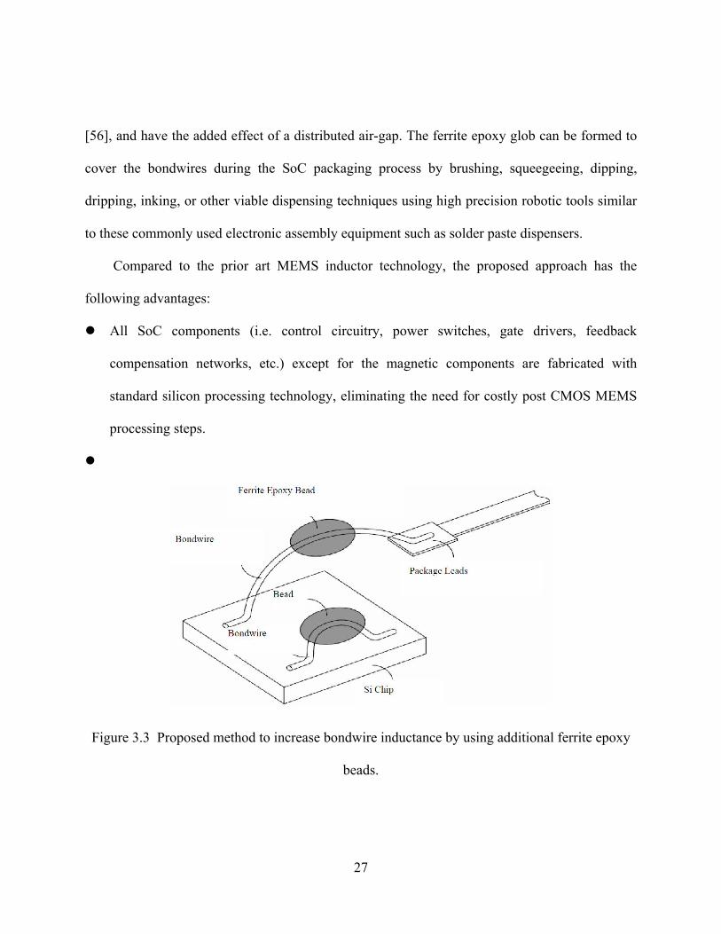
Figure 3.3 Proposed method to increase bondwire inductance by using additional ferrite epoxy
beads.
Page 45
28
The on-chip bondwire inductors and transformers can be integrated into the power SoC
packaging process with minimal changes. This opens enormous possibilities for realizing
cost-effective, high current, high efficiency with improved reliability power SoC’s.
Aluminum or gold bondwires are substantially more conductive than the thin metal films in
MEMS inductors. A much lower dc resistance and higher Q factor can be expected for the
bondwire inductors because aluminum or gold bondwires have large diameters than the thin
films used in MEMS, and the material resistivity is also higher. Quality factor Q is the ratio
of reactive impedance to equivalent series resistance (ESR), an important parameter of
inductor performance. High Q leads to low power dissipation and a higher efficiency of the
power converter.
The electromagnetic field of a bondwire inductor is mainly distributed outside the silicon
substrate. The eddy current loss in the silicon substrate at high frequency, a major concern in
MEMS magnetics, can therefore be minimized.
3.2 Finite Element Modeling Tools
In this research, we use finite element modeling tools like Ansoft HFSS and Maxwell 3D.
HFSS is the industry-standard software for S-parameter, Full-Wave SPICE extraction, and 3D
electromagnetic field simulation of high-frequency and high-speed components. Engineers rely
on the accuracy, capacity, and performance of HFSS to design on-chip embedded passives, IC
packages, PCB interconnects, antennas, RF/microwave components, and biomedical devices.
Page 46
29
HFSS improves engineering productivity, reduces development time, and better assures first-pass
design success.
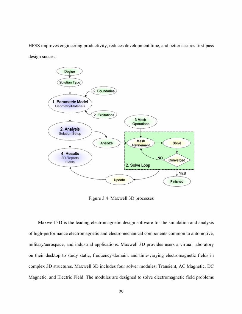
Figure 3.4 Maxwell 3D processes
Maxwell 3D is the leading electromagnetic design software for the simulation and analysis
of high-performance electromagnetic and electromechanical components common to automotive,
military/aerospace, and industrial applications. Maxwell 3D provides users a virtual laboratory
on their desktop to study static, frequency-domain, and time-varying electromagnetic fields in
complex 3D structures. Maxwell 3D includes four solver modules: Transient, AC Magnetic, DC
Magnetic, and Electric Field. The modules are designed to solve electromagnetic field problems
Page 47
30
in the time and frequency domains. Each model uses 3D Finite Elements and automatic adaptive
meshing techniques to compute the electrical/electromagnetic behavior of low-frequency
components. With Maxwell 3D, users solve for electromagnetic-field parameters, such as force,
torque, capacitance, inductance, resistance, and impedance, as well as generate state-space
models, visualize 3D electromagnetic fields, and optimize design performance. [57]
The proposed bondwire inductor and transformer structures were modeled and analyzed
using the electromagnetic simulation tool HFSS and Maxwell 3D from Ansoft [57]. We use
HFSS as a high-performance full-wave electromagnetic (EM) finite element simulator for
arbitrary 3D passive component modeling in high frequency. The objective here is to investigate
the effect of ferrite epoxy glob coating on the inductance value and coupling effect of bondwires
using EM simulation. Furthermore, EM modeling helps optimize bondwire inductor and
transformer design in terms of physical dimensions of bondwire, ferrite coating shape, coating
position, coating thickness, and the ferrite material type used. HFSS may be perfect modeling
tool for new generation power application. However, in low frequency, say, below 10MHz, when
traditional power passive components applications take dominance, we use Maxwell 3D to get
accuracy. Maxwell is more for electro-mechanical devices such as relays, motors while HFSS is
more for electronic devices such as waveguides, strip lines. Maxwell is a used for a quasi-static
analysis, in other words includes only TEM mode. It is accurate only at reasonably low
frequencies, but for a full wave analysis we need to use HFSS
Page 48
31
Figure 3.5 HFSS processes
In a word, when it comes to passive components like inductors and transformers, HFSS is
preferred in high frequency and/or small size simulation while Maxwell is preferred in low
frequency and /or large size simulation.
Page 49
32
CHAPTER 4: BONDWIRE INDUCTOR
4.1 Proposed Bondwire Inductor
The proposed bondwire inductor structure is modeled and analyzed with the
electromagnetic simulation tool HFSS from Ansoft [57]. Fig. 3.2 shows the HFSS model of the
proposed bondwire inductor with a uniform coating of ferrite epoxy. The objective here is to
investigate the effect of ferrite epoxy coating on the inductance value of bondwires using EM
simulation. Furthermore , EM modeling helps optimize bondwire inductor design parameters
such as the physical dimensions of bondwire, ferrite coating shape, coating position, coating
thickness, and the ferrite material used.
HFSS simulation generates a set of S parameters from the inductor structure which are then
converted to a set of Y parameters. The effective quality factor Q and inductance L can be then
extracted from the Y parameters by using the following equations
)Im(1
11yL ffe ω
−= (1)
)Re()Im(
11
11
yyQ −= (2)
Page 50
33
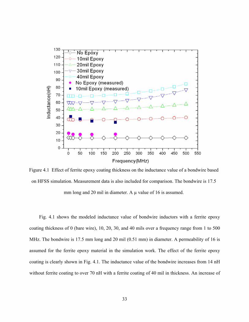
Fig. 4.1 shows the modeled inductance value of bondwire inductors with a ferrite epoxy
coating thickness of 0 (bare wire), 10, 20, 30, and 40 mils over a frequency range from 1 to 500
MHz. The bondwire is 17.5 mm long and 20 mil (0.51 mm) in diameter. A permeability of 16 is
assumed for the ferrite epoxy material in the simulation work. The effect of the ferrite epoxy
coating is clearly shown in Fig. 4.1. The inductance value of the bondwire increases from 14 nH
without ferrite coating to over 70 nH with a ferrite coating of 40 mil in thickness. An increase of
Figure 4.1 Effect of ferrite epoxy coating thickness on the inductance value of a bondwire based
on HFSS simulation. Measurement data is also included for comparison. The bondwire is 17.5
mm long and 20 mil in diameter. A µ value of 16 is assumed.
Page 51
34
a factor of 5 in inductance value can be observed with the application of a 40 mil ferrite epoxy
coating over the bondwire.
Figure 4.2 The bondwire is 17.5 mm long and 20 mil in diameter. A thickness of 20 mils is
assumed for the ferrite epoxy coating.
A set of measurement data is included in Fig. 4.1 for comparison with the modeling result.
A reasonably good agreement can be seen between the modeling and measurement results. This
gives us confidence to use Ansoft HFSS as the modeling tool in our study of bondwire inductors.
Key bondwire inductor design parameters include length and diameter of the bondwire, and
thickness and permeability of the ferrite epoxy coating. It is observed in Fig. 4.1 that the
inductance of the wirebond inductor increases with ferrite epoxy coating thickness since a larger
Page 52
35
ferrite thickness leads to less magnetic relunctance, more magnetic flux, and greater inductance.
However, there are practical limitations on how much ferrite epoxy coating can be applied into
the IC package which has a limited space.
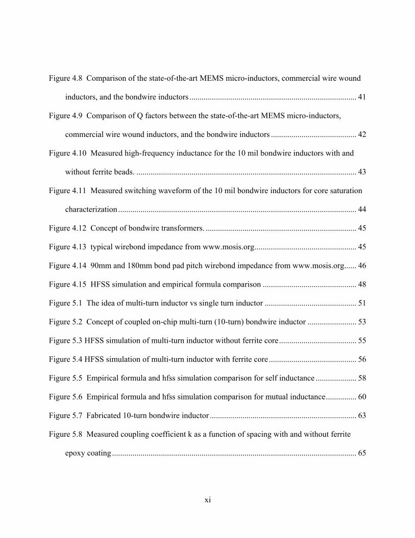
Fig. 4.2 shows the modeled inductance value of bondwire inductors with a ferrite epoxy
permeability of 1 (bare wire), 9, 16, 25, 36, and 49 over a frequency range from 1 to 500 MHz.
Naturally, the inductance value increases with increasing permeability of the ferrite epoxy
material. Iron oxide based ferrite ceramic materials usually demonstrate a relative permeability
up to a few thousands. Ferrite epoxy materials with mixed ferrite powders and organic binder
tend to have a much lower effective permeability in a range of 9 to 20 depending on the loading
percentage of the ferrite powders. For example, the permeability of the ferrite epoxy used in our
experimental study from Methode Development Corporation is between 12 and16. However, it is
possible that new high-µ ferrite epoxy materials can be developed in the future. The simulation
results indicate that the inductance of a bare bondwire can be increase by a factor of 10 if a µ
value of 50 can be used.
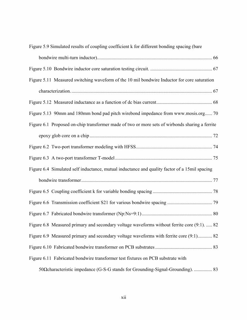
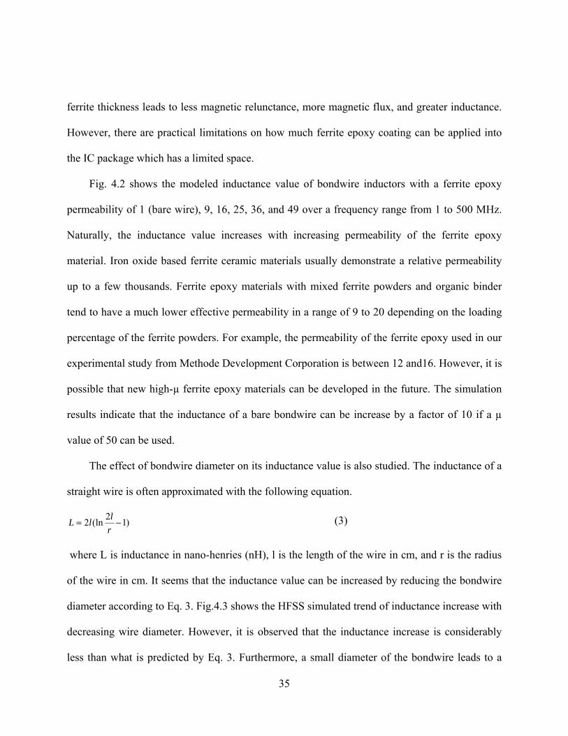
The effect of bondwire diameter on its inductance value is also studied. The inductance of a
straight wire is often approximated with the following equation.
)12(ln2 −=rllL (3)
where L is inductance in nano-henries (nH), l is the length of the wire in cm, and r is the radius
of the wire in cm. It seems that the inductance value can be increased by reducing the bondwire
diameter according to Eq. 3. Fig.4.3 shows the HFSS simulated trend of inductance increase with
decreasing wire diameter. However, it is observed that the inductance increase is considerably
less than what is predicted by Eq. 3. Furthermore, a small diameter of the bondwire leads to a
Page 53
36
high dc series resistance and a small Q factor. Therefore, it may not be an effective solution to
increase the inductance by using very thin bondwires in power SoC’s.
Figure 4.3 Inductance of bondwires with a diameter of 5, 10, and 20 mils based on HFSS
simulation. The bondwire is 17.5 mm
In short, the EM simulation work indicates that the bondwire inductance can be increased
by increasing the thickness and permeability of the ferrite epoxy coating, and to a less extent, by
using thinner bondwires.
Page 54
37
4.2 Experiment Results
We have conducted experimental investigation of the proposed on-chip bondwire inductor
concept using two types of ferrite epoxy composite materials. The first material is a custom
formulated magnetic epoxy comprised of manganese-zinc (MgZn) ferrite powder with an
average particle size of 10 µm, thermoplastic resin, and solvent from Methode Development
Corporation. The manganese-zinc ferrite loading powder is commercially available (Steward
73300). The average surface area of the powder is 1.4 m2/g. The saturation moment of the bulk
powder is 79.4 emu/g. The cured ferrite composite (no solvent) consisted of 96% by mass ferrite
with the balance consisting of polymer. The effective permeability is between 12 and16. The
second material is a ferrite nano composite from Inframat Corporation that is comprised of very
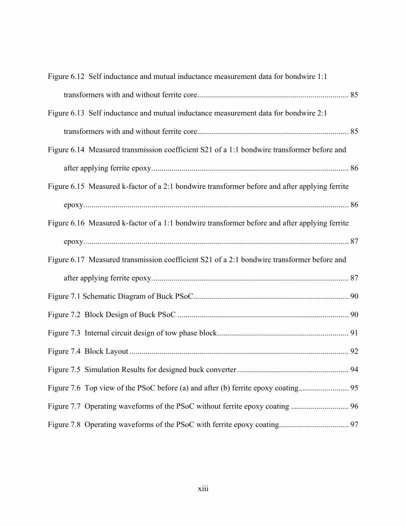
fine (NiZn)Fe2O4 nano particles with an average size of 5-15 nm and a commercial epoxy.
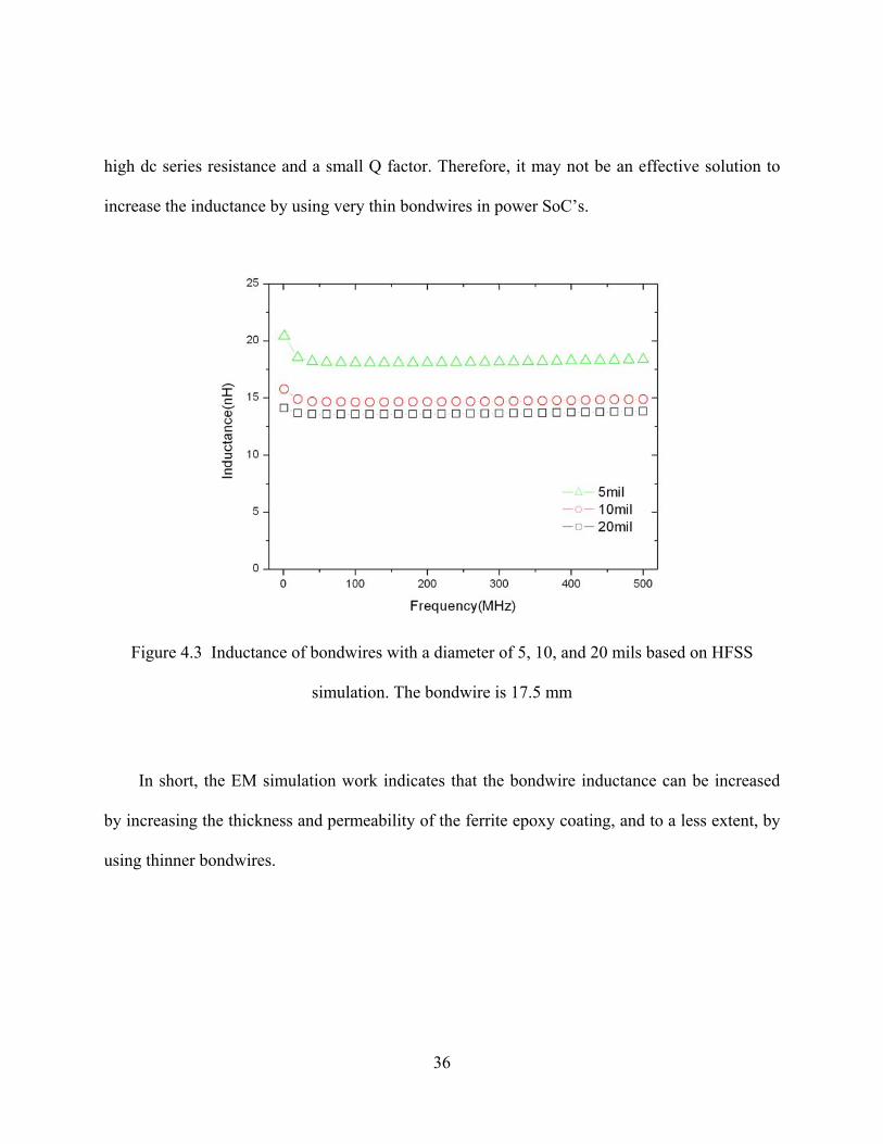
Figure 4.4 Photo of aluminum bondwires with and without ferrite epoxy coating on a PCB
substrate.
Page 55
38
The test reported herein was conducted on standalone copper and aluminum wires initially
and then on aluminum bondwires bonded onto a PCB substrate. Copper wires with a fixed length
of 20 mm but two different diameters of 250µm (10 mil) and 500 µm (20 mil) were used to
emulate the bondwires in IC packages. Note that copper has a slightly lower resistivity than more
commonly used gold or aluminum. The ferrite epoxy materials were manually brushed onto the
copper bondwire to form a ferrite bead. Curing consisted of a thermal treatment of the ferrite
beads in an oven at 140oC for 30 minutes for both ferrite epoxy material options. The ferrite-
polymer composites display negligible conductivity and therefore are electrically self-isolated
from the bare copper bondwires. Fig. 4.4 shows a photo of aluminum bondwires with and
without the ferrite epoxy bead on the PCB substrate. The wirebonding was conducted on an
Electrodyne M20 wirebonder using 5 mil aluminum bondwires.
Figure 4.5 Simplified equivalent circuit model of bondwire inductors used to extract L and Q
from S-parameters.
Page 56
39
The bondwire inductors were characterized with an HP 4284A high precision LCR meters
in a low frequency range up to 1MHz. DC resistance was measured with an Instek 801H milli-
ohm meter. High frequency measurement was performed using an Agilent 8753 S-parameter
network analyzer. The effective quality factor Q and inductance L can be then extracted from the
Y parameters by using Equations (1) and (2). Fig. 4.5 illustrates the simplified equivalent model
of the bondwire inductor that we used in electrical parameter extraction.
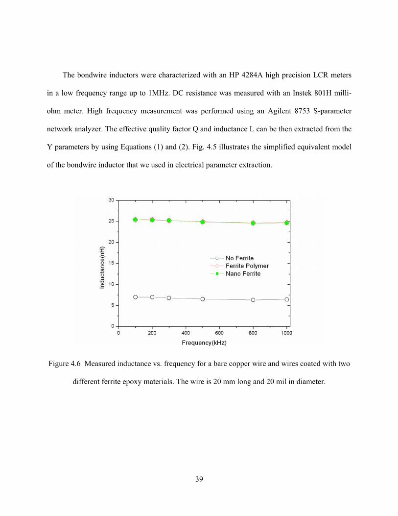
Figure 4.6 Measured inductance vs. frequency for a bare copper wire and wires coated with two
different ferrite epoxy materials. The wire is 20 mm long and 20 mil in diameter.
Page 57
40
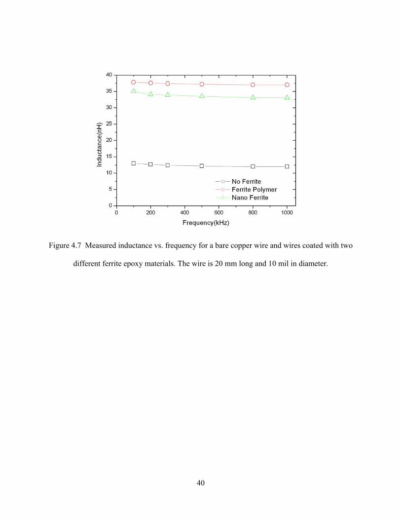
Figure 4.7 Measured inductance vs. frequency for a bare copper wire and wires coated with two
different ferrite epoxy materials. The wire is 20 mm long and 10 mil in diameter.
Page 58
41
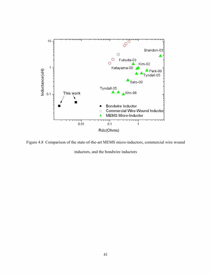
Figure 4.8 Comparison of the state-of-the-art MEMS micro-inductors, commercial wire wound
inductors, and the bondwire inductors
Page 59
42
Figure 4.9 Comparison of Q factors between the state-of-the-art MEMS micro-inductors,
commercial wire wound inductors, and the bondwire inductors
Figs. 4.6 and 4.7 show the measured inductance for the 10 mil and 20 mil bondwire
inductors with no ferrite bead, the ferrite polymer bead, and the ferrite nano-composite bead
respectively. The inductance of bare copper wires was increased by a factor of 2.8 to 3.5 with the
addition of the ferrite epoxy beads. The dc resistance of the 10 mil and 20 mil bondwire
inductors was measured as 7.1 mΩ and 1.7 mΩ respectively using an Instek 801H milli-ohm
meter. The 10 mil bondwire inductor demonstrates an inductance of 38 nH and a dc resistance of
7.1 mΩ. Fig. 4.8 compares the state-of-the-art MEMS micro-inductors, commercial wire-wound
inductors, and the bondwire inductors in this work in terms of inductance and dc winding
Page 60
43
resistance achieved. It is clearly shown that the bondwire inductors offer a solution for high
current power SOC applications in which the MEMS micro-inductors fall short. Fig. 4.9
compares the Q-factor of the three approaches. The bondwire inductors demonstrate a Q factor
of 30-40 in a frequency range of 2 to 20 MHz, similar to that of the commercial wire-wound
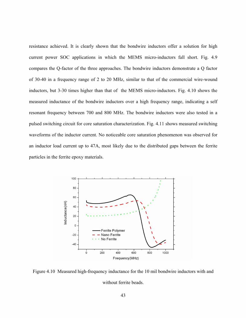
inductors, but 3-30 times higher than that of the MEMS micro-inductors. Fig. 4.10 shows the
measured inductance of the bondwire inductors over a high frequency range, indicating a self
resonant frequency between 700 and 800 MHz. The bondwire inductors were also tested in a
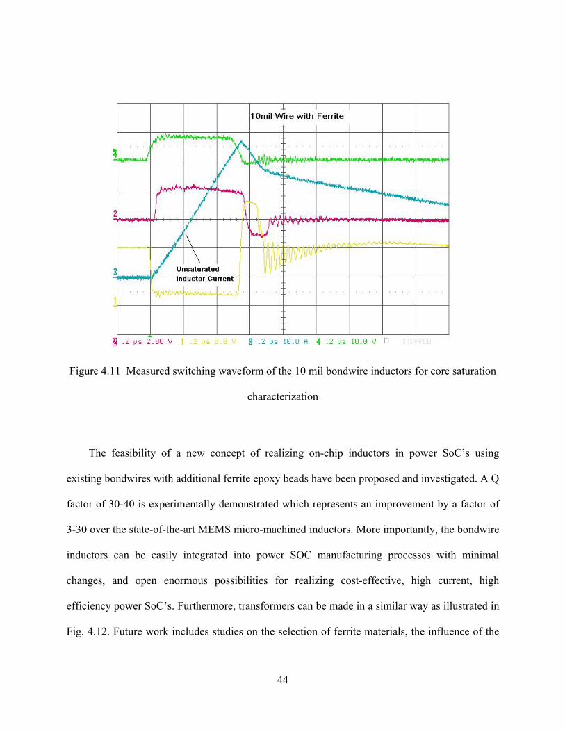
pulsed switching circuit for core saturation characterization. Fig. 4.11 shows measured switching
waveforms of the inductor current. No noticeable core saturation phenomenon was observed for
an inductor load current up to 47A, most likely due to the distributed gaps between the ferrite
particles in the ferrite epoxy materials.
Figure 4.10 Measured high-frequency inductance for the 10 mil bondwire inductors with and
without ferrite beads.
Page 61
44
Figure 4.11 Measured switching waveform of the 10 mil bondwire inductors for core saturation
characterization
The feasibility of a new concept of realizing on-chip inductors in power SoC’s using
existing bondwires with additional ferrite epoxy beads have been proposed and investigated. A Q
factor of 30-40 is experimentally demonstrated which represents an improvement by a factor of
3-30 over the state-of-the-art MEMS micro-machined inductors. More importantly, the bondwire
inductors can be easily integrated into power SOC manufacturing processes with minimal
changes, and open enormous possibilities for realizing cost-effective, high current, high
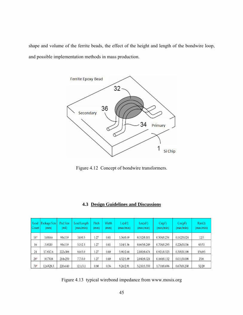
efficiency power SoC’s. Furthermore, transformers can be made in a similar way as illustrated in
Fig. 4.12. Future work includes studies on the selection of ferrite materials, the influence of the
Page 62
45
shape and volume of the ferrite beads, the effect of the height and length of the bondwire loop,
and possible implementation methods in mass production.
Figure 4.12 Concept of bondwire transformers.
4.3 Design Guidelines and Discussions
Figure 4.13 typical wirebond impedance from www.mosis.org
Page 63
46
Figure 4.14 90mm and 180mm bond pad pitch wirebond impedance from www.mosis.org
There is a good way to predict the bondwire inductance by checking the specific packaging
characterization from data sheet like Figure 4.13 and Figure 4.14. If using just one bondwire as a
inductor, the self inductance can be extracted directly form the impedance form or curve. We
will talk about the mutual effect in the fifth chapter. While doing the design for single bondwire
inductor, we want to minimize the mutual inductance by enlarge the distance between this
bondwire and the other bondwires.
In order to determine which pad pitch to use, we need to roughly predict the length and
diameter of the bondwire we want to use.
Some first-order formulas to calculate the inductance value are [58]:
)](4
25.1)2[ln(2.0 nHlr
rllL μ
++−= (4)
u is the conductor permeability which is 1 in all bondwire cases.
Page 64
47
So that we have:
)](0.1)2[ln(2.0 nHlr
rllL +−= (5)
If r<<l in most bondwire cases
)](0.1)2[ln(2.0 nHrllL −= (6)
r: radius of the crossing section of inductor (mm)
l: length of the bondwire inductor (mm)
L: Bondwire inductance in nH
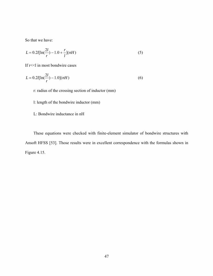
These equations were checked with finite-element simulator of bondwire structures with
Ansoft HFSS [53]. Those results were in excellent correspondence with the formulas shown in
Figure 4.15.
Page 65
48
Figure 4.15 HFSS simulation and empirical formula comparison
Before we get to the design guideline for bondwire inductor, the ferrite polymer effect
should be well considered. The traditional formula for coil inductor with magnetic core is not
true for bondwire inductor with ferrite coating anymore. HFSS simulations have been done to
determine the ferrite coating effect.
αμμ =eff (7)
The μ is defined as ferrite material permeability. Effective permeability μeff is defined as a
multiple of inductance before and after ferrite coat. α is a constant for each magnetic material, it
depends on the ferrite powder, concentration and the curing process. The μeff must be calibrated
before use for specific ferrite polymer and curing process. For the magnetic coating used in this
work, the constant is around 0.75.
Page 66
49
)(]0.1)2[ln(2.0 0 nHLrllL effeff ⋅=−⋅= μμ (8)
L0 is defined as original inductance for bondwire or bare bondwire inductance here.
There are three ways to design a bondwire inductor.
A. Finite element simulator like Ansoft HFSS and Maxwell 3D
B. Empirical Formula
C. Bonding machine or packaging Datasheet
By using finite element simulator like Ansoft HFSS and Maxwell 3D, the inductance and Q
factor can be calculated. However, you may need software licenses and some software expertise.
The Empirical design procedures are as follows:
1) Determine the inductance L and dc resistance Rdc for the inductor
2) Choose the magnetic ink and get the relative permeability μr from the company
3) Calibrate the ferrite ink to get the effective permeability μeff
4) Get the bare wire inductance Lo from equation as below:
)(]0.1)2[ln(2.0 0 nHLrllL effeff ⋅=−⋅= μμ
5) Get the bondwire length by formula )](0.1)2[ln(2.0 nHlr
rllL +−= with several possible
diameters
6) After checking with your space limitation and bonding machine capability, determine the
single bondwire length l0 and how many bonds you need.
7) Choose the bondwire diameter for this specific dc resistance
Page 67
50
The bonding machine or packaging datasheet design procedures are as follows:
1) Determine the inductance L and dc resistance Rdc for the inductor
2) Choose the magnetic ink and get the relative permeability μr from the company
3) Calibrate the ferrite ink to get the effective permeability μeff
4) Get the bare wire inductance Lo from equation as below
)(]0.1)2[ln(2.0 0 nHLrllL effeff ⋅=−⋅= μμ
5) Determine the individual bondwire length l and number of bondwire N
6) Check the dc resistance in the corresponding column in the datasheet. The total dc
resistance is N×rdc.
7) Choose the bondwire diameter for this specific dc resistance which meets the IC
specification.
Page 68
51
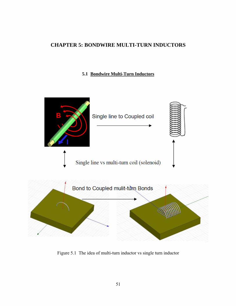
CHAPTER 5: BONDWIRE MULTI-TURN INDUCTORS
5.1 Bondwire Multi-Turn Inductors
Figure 5.1 The idea of multi-turn inductor vs single turn inductor
Page 69
52
The experimental results for a single bondwire inductor with improved dc resistance and Q
factor in comparing to MEMS inductors was reported in [52]-[54]. However, the single bondwire
yielded low inductance for PSoC or PSiP application. Several US patents have addressed this
issue by suggesting the use of multiple bondwires connected in series [47]-[50], but suffer from
the drawback of increased footprint. Actually, there is a better way to achieve better performance.
Let’s take a look at solenoid inductor. For solenoid inductor,
1) All flux is within the coil (no leakage flux)
2) All flux links each turn
The self inductance of a tightly wounded solenoid with N turn and cross-section area A and
length L is given by
lAN
L ro2μμ
= (9)
In this chapter, by exploring the coupling effect, this deficiency is addressed by a multi-turn
bondwire inductor leading to increased inductance and Q factor. As shown in Fig. 5.1, a set of
closed placed multiple wirebonds is very similar to a solenoid where the magnetic flux is shared
by all bondwire loops. There is a strong coupling effect among those bondwire loops depending
on how close they are placed to each other. Today’s automatic wirebonders can place bondwires
as close as several tens of micrometers.
Page 70
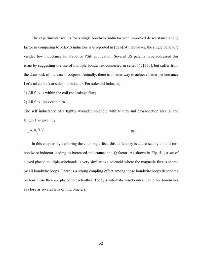
53
Figure 5.2 Concept of coupled on-chip multi-turn (10-turn) bondwire inductor
A tightly coupled multi-turn bondwire may be approximated to the solenoid for the purpose
of the present analysis; such a construction is illustrated in Fig.5.2. We proposed to use ferrite
epoxy glob cores to increase inductance and improve coupling effect as shown in Fig.5.2.
Bondwire inductors can be constructed between the chip and package leads or between pads on
the chip.
The proposed bondwire inductor structures were modeled and analyzed using the
electromagnetic simulation tool HFSS from Ansoft [57]. The HFSS tool was used to investigate
the effect of adding a ferrite epoxy glob coating to the multi-turn bondwire and in turn to
evaluate the effect on inductance and Q factor. Furthermore, HFSS modeling was used to
Page 71
54
optimize bondwire inductor design in terms of physical dimensions of the bondwires and ferrite
core, and the ferrite core material used.
The HFSS simulation generates a set of S parameters from the bondwire inductor structure
which are then converted to a set of Y parameters. The effective quality factor Q and inductance
L can be then extracted from the Y parameters by using the following equations
)Im(1
11yL ffe ω
−= (10)
)Re()Im(
11
11
yyQ −=
(11)
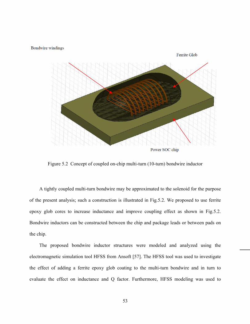
Fig. 5.3 shows the modeled inductance values of a single-turn (with a total bondwire length
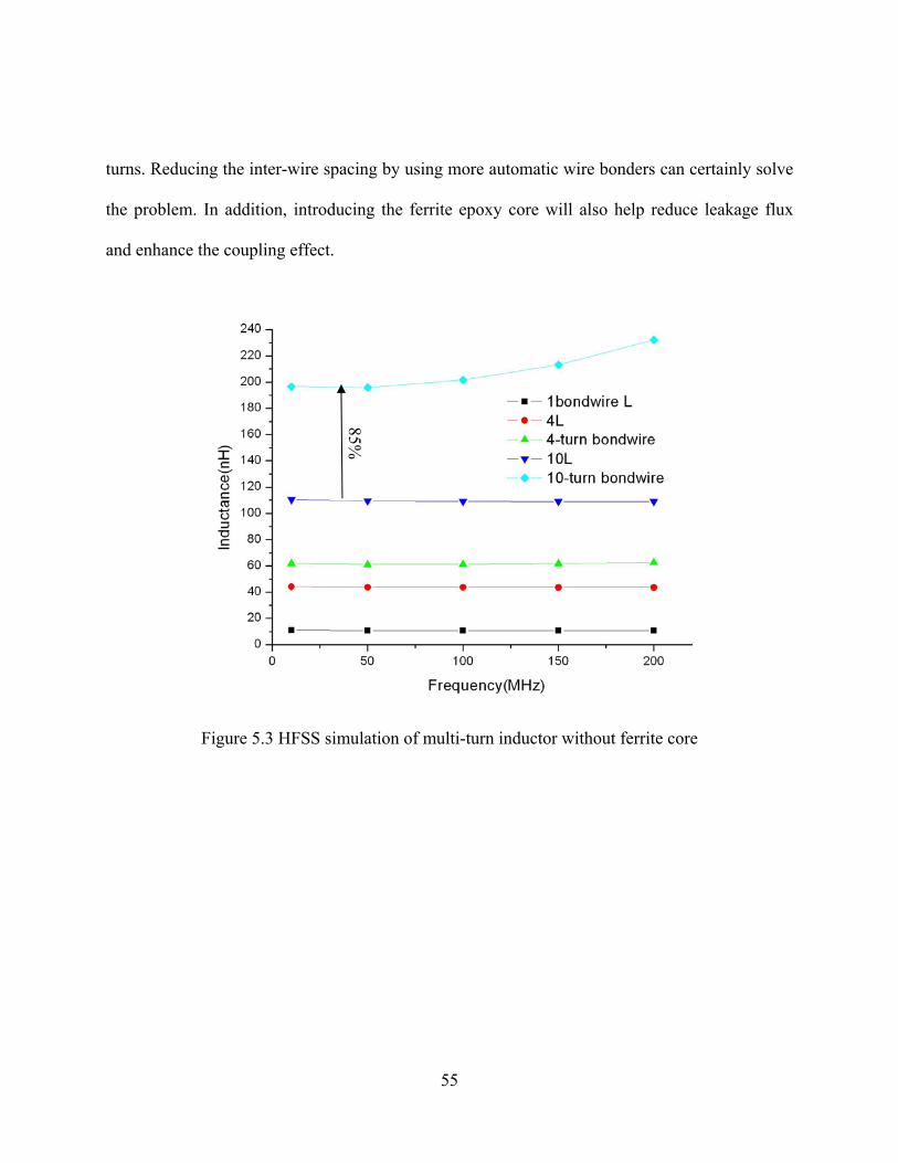
L), four-turn, and ten-turn bondwire constructions without ferrite epoxy core. Note that all the
bondwire loops share the same shape and dimensions. In addition, the inductance values of two
single-turn bondwire inductors with an equivalent bondwire length of 4L and 10L respectively
are also plotted on the same graph for comparison. The 4L and 10L single-turn inductors have
the same total bondwire length as the 4-turn and 10-turn inductors respectively but obviously do
not have any coupling effect as observed in their multi-turn counterparts. It is observed that the
10-turn inductor shows an inductance value of roughly 200nH at 10MHz as compared to 110nH
for the single-turn 10L inductor. The increase in inductance due to the coupling effect between
the individual turns is desirable but far below what an ideal solenoid offers. Instead of a factor of
10 increase based on Equation (1), we only observe an increase of 85% in inductance, indicating
a weak coupling between the individual turns. This is due to the fact that the spacing between
two adjacent bondwires is 750 µm or greater limited by the Orthodyne Model 20 manual wire
bonder used, resulting in considerable leakage flux and weak coupling between the individual
Page 72
55
turns. Reducing the inter-wire spacing by using more automatic wire bonders can certainly solve
the problem. In addition, introducing the ferrite epoxy core will also help reduce leakage flux
and enhance the coupling effect.
Figure 5.3 HFSS simulation of multi-turn inductor without ferrite core
85%
Page 73
56
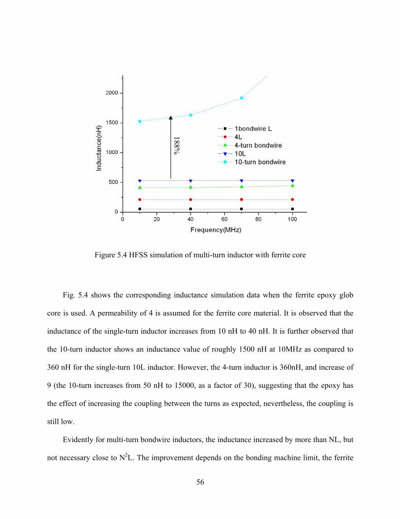
Figure 5.4 HFSS simulation of multi-turn inductor with ferrite core
Fig. 5.4 shows the corresponding inductance simulation data when the ferrite epoxy glob
core is used. A permeability of 4 is assumed for the ferrite core material. It is observed that the
inductance of the single-turn inductor increases from 10 nH to 40 nH. It is further observed that
the 10-turn inductor shows an inductance value of roughly 1500 nH at 10MHz as compared to
360 nH for the single-turn 10L inductor. However, the 4-turn inductor is 360nH, and increase of
9 (the 10-turn increases from 50 nH to 15000, as a factor of 30), suggesting that the epoxy has
the effect of increasing the coupling between the turns as expected, nevertheless, the coupling is
still low.
Evidently for multi-turn bondwire inductors, the inductance increased by more than NL, but
not necessary close to N2L. The improvement depends on the bonding machine limit, the ferrite
188%
Page 74
57
material and the turn number. As shown in Fig. 5.3 and Fig. 5.4, with and without ferrite glob,
we get 40% and 74% boosting respectively for 4-turn bondwire inductor, and we get 85% and
188% respectively boosting for 10-turn bondwire inductor.
There are two ways to calculate the bondwire inductance. The first one is about the inductor
itself. The second one also considers the average height h of the bondwire to the perfectly
conducting ground plane from [58].
)](2[2.0)2[ln(2
0 nHrhInl
rhlL ==
πμ
(12)
Some first-order formulas to calculate the inductance value without considering ground
plate are [58]:
)](4
25.1)2[ln(2.0 nHlr
rllL μ
++−= (13)
u is the conductor permeability which is 1 in all bondwire cases.
So that we have:
)](0.1)2[ln(2.0 nHlr
rllL +−=
(14)
If r<<l in most bondwire cases
)](0.1)2[ln(2.0 nHrllL −=
(15)
r: radius of the crossing section of inductor (mm)
l: length of the bondwire inductor (mm)
L: Bondwire inductance in nH
Page 75
58
For power SoC application, the ground plate lies at the back of the PCB or silicon chip. The
average height of bondwire on PCB is 1.25mm. The thickness of PCB is 0.8mm. The average
height is 3.1mm. The length of bondwire is 5mm. Let’s compare equation 12 and 15 as:
)49.3(2.0)](2[2.0)2[ln(2
0 lnHrhInl
rhlL ===
πμ
)4.3(2.0)](0.1)2[ln(2.0 lnHrllL =−=
The positions of the ground plane do affect the inductance in the power system. Since the
difference between these two calculations is so small that we can just neglect it and to avoid the
complexity it may bring to the calculation, we decided to consider the inductor itself for
simplification. For the bondwire inductor itself, the equation 15 is used in this chapter for
empirical formula and simplification.
Figure 5.5 Empirical formula and hfss simulation comparison for self inductance
Page 76
59
These equations were checked with finite-element simulator of bondwire structures with
Ansoft HFSS [57]. Those results were in excellent correspondence with the formulas shown in
Fig.5.5.
)(]0.1)2[ln(2.0 0 nHLrllL effeff ⋅=−⋅= μμ
(16)
The μ is defined as ferrite material’s relative permeability. Effective permeability μeff is
defined as a multiple of inductance before and after ferrite coat, which depends on the ferrite
powder, concentration and the curing process. The μeff must be calibrated before use for specific
ferrite polymer and curing process.
L0 is defined as bare wire inductance for bondwire.
For bondwires with ferrite coating, the mutual inductance may be defined as:
)(1)1ln(2.0 0
22
nHMld
ld
dl
dllM effeff ⋅=
⎥⎥⎦
⎤
⎢⎢⎣
⎡+⎟
⎠⎞
⎜⎝⎛+−⎟
⎠⎞
⎜⎝⎛++⋅= μμ
(17)
)(1)1ln(2.022
0 nHld
ld
dl
dllM
⎥⎥⎦
⎤
⎢⎢⎣
⎡+⎟
⎠⎞
⎜⎝⎛+−⎟
⎠⎞
⎜⎝⎛++=
(18)
Like L0, M0 is defined as barewire mutual inductance which means mutual inductance of
bare bondwire (no ferrite coating) here.
When the distance between two bondwire is very small, which means the d<<l, the mutual
inductance M become noticeable.
ld << => 1>>
dl
Page 77
60
dl
dl
≈⎟⎠⎞
⎜⎝⎛+
2
1 ,
112
≈⎟⎠⎞
⎜⎝⎛+
ld
, 0≈
ld
)(12ln2.00 nHdllM ⎟⎟
⎠
⎞⎜⎜⎝
⎛−⎟
⎠⎞
⎜⎝⎛=
(19)
Figure 5.6 Empirical formula and hfss simulation comparison for mutual inductance
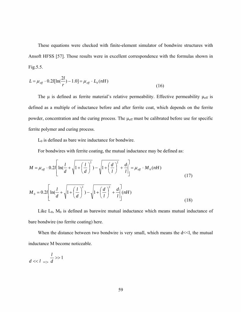
In our bondwire case, the first order approximation is not accurate enough, the number in
equation 11 need to be modified a little bit to fit the hfss simulation results like Fig.5.6.
)(5.12ln2.00 nHdllM ⎟⎟
⎠
⎞⎜⎜⎝
⎛−⎟
⎠⎞
⎜⎝⎛=
(20)
For N turn bondwire inductor, the barewire inductance L0,TOT can be expressed as below:
Page 78
61
( ) ( ) ( ) ( ) )(2...32221212 1,04,03,02,01,00,0 nHMMNMNMNMNNLL NTOT −++−+−+−+−+=
or ( ) )(21
1,00,0 nHMmNNLL
Nm
mmTOT ∑
−=
=
−+= (21)
Where
)](0.1)2[ln(2.00 nHrllL −=
)(12ln2.00
1,0 nHd
llM ⎟⎟⎠
⎞⎜⎜⎝
⎛−⎟⎟
⎠
⎞⎜⎜⎝
⎛=
)(122ln2.0
02,0 nH
dllM ⎟
⎟⎠
⎞⎜⎜⎝
⎛−⎟⎟
⎠
⎞⎜⎜⎝
⎛=
)(132ln2.0
03,0 nH
dllM ⎟
⎟⎠
⎞⎜⎜⎝
⎛−⎟⎟
⎠
⎞⎜⎜⎝
⎛=
)(1)1(
2ln2.00
1,0 nHdN
llM N ⎟⎟⎠
⎞⎜⎜⎝
⎛−⎟⎟
⎠
⎞⎜⎜⎝
⎛−
=−
01)1(
2ln0
≥−⎟⎟⎠
⎞⎜⎜⎝
⎛− dN
l
=>1
)1(2ln
0
≥⎟⎟⎠
⎞⎜⎜⎝
⎛− dN
l
=>e
dNl
≥− 0)1(2
=> 2)1(
0
−≥
Nedl
Page 79
62
So when )1(2
0 −≥
Neld
, the mutual inductance can be neglected.
For most of the cases, when 4≥N , the mutual inductance can be neglected, so the equation
can be expressed as below:
( ) ( ) ( ) )(221212 3,02,01,00,0 nHMNMNMNNLL TOT −+−+−+≈ (22)
( ) ( ) ( )( ) )(221212 3,02,01,00,0 nHMNMNMNNLLL effTOTeffTOT −+−+−+≈= μμ (23)
5.2 Experiment Results
This section describes the experimental validation of the proposed multi-turn bondwire
inductor concept using the ferrite epoxy composite materials. The material is a custom
formulated magnetic epoxy comprised of manganese-zinc (MgZn) ferrite powder with an
average particle size of 10 µm, thermoplastic resin, and solvent from Methode Development
Corporation. The manganese-zinc ferrite loading powder is commercially available (Steward
73300). The average surface area of the powder is 1.4 m2/g. The saturation moment of the bulk
powder is 79.4 emu/g. The cured ferrite composite (no solvent) consisted of 96% by mass ferrite
with the balance consisting of polymer. The relative permeability from manufacturer’s datasheet
is between 12 and16.
Page 80
63
Figure 5.7 Fabricated 10-turn bondwire inductor
A 10-turn aluminum bondwire inductor is made on a PCB substrate initially to verify the
concept as shown in Fig. 5.7. The measured dc resistance of the 10-turn inductor is 130mΩ. The
ferrite epoxy material is manually brushed onto the bondwire to form a ferrite glob core. The
ferrite epoxy core is then cured at 140oC for 30 minutes in atmosphere. The ferrite-polymer
composite displays a very high resistivity and provides sufficient electrical insulation between
the bondwires. Tables 2 and 3 summarize measured bondwire inductance of three spacing
between the turns for without and with the ferrite epoxy core respectively. An Agilent E4980
precision LCR meter is used in the measurement. We include the equivalent inductance of ten
single-turn bondwire inductors in series as a comparison.
Page 81
64
Table 2 Measured bondwire inductance without the ferrite epoxy core
Inter-turn Spacing Inductance of 10-turn
inductor
Inductance of 10
single-turn
inductors in series
% of Inductance
increase due to
coupling effect
50 mil or 1.25 mm 52.5 nH 40 nH 31%
45 mil or 1.125 mm 55.5 nH 40 nH 36%
30 mil or 0.75 mm 74 nH 40 nH 85%
Table 3 Measured bondwire inductance with the ferrite epoxy core
Inter-turn Spacing Inductance of 10-turn
inductor
Inductance of 10
single-turn
inductors in series
% of Inductance
increase due to
coupling effect
50 mil or 1.25 mm 286 nH 180 nH 59%
45 mil or 1.125 mm 290 nH 180 nH 60%
30 mil or 0.75 mm 340 nH 180 nH 89%
It is observed that inductance of the 10-turn bondwire inductor has increased from 74 nH to
340 nH after the ferrite epoxy core is used, yielding a Q factor of 28 at 5 MHz. Furthermore, the
inductance of a 10-turn bondwires is much greater than the equivalent inductance of ten single-
turn bondwire inductors in series due to the mutual coupling effect. The coupling effect becomes
more pronounced with decreasing spacing between the multiple bondwires as expected. In the
Page 82
65
case of ferrite epoxy core not being used, there is an 85% increase of inductance value due to
coupling effect for a spacing of 30 mils. That is in good agreement with the modeling result in
previous sub-chapter. However, in the case of ferrite epoxy core being used, there is only an 89%
increase of inductance value due to coupling effect for a spacing of 30 mils, far below the 188%
increase projected by our HFSS simulation. The discrepancy may be due to the relative
permeability value being overestimated in HFSS simulation.
Figure 5.8 Measured coupling coefficient k as a function of spacing with and without ferrite
epoxy coating
Fig. 5.8 shows the experimentally characterized coupling coefficient k as a function of
inter-turn spacing for the case with and without the ferrite epoxy core. It is observed that the
coupling factor k of the bondwire inductor with ferrite epoxy core is higher than the case without
Page 83
66
the ferrite core, and less dependent on the inter-turn spacing. Fig. 5.9 shows the simulated
coupling coefficient k for several inter-turn spacing without using ferrite epoxy core. The spatial
separation between the turns leads to a large leakage flux and reduced mutual coupling,
especially when ferrite epoxy core is not used. The data show that the coupling effect can
beenhanced with the spacing between bondwires being reduced. It should be noted that
automatic bonding machines currently used in the IC packaging industry can routinely achieve a
bond to bond pitch less than 0.2 mm or 8 mils, potentially enabling highly coupled bondwire
inductors. In general, the coupling effect can be enhanced through reduction of bond pitch and
use of ferrite epoxy materials with a higher permeability.
Figure 5.9 Simulated results of coupling coefficient k for different bonding spacing (bare
bondwire multi-turn inductor)
Page 84
67
Figure 5.10 Bondwire inductor core saturation testing circuit.
Figure 5.11 Measured switching waveform of the 10 mil bondwire Inductor for core saturation
characterization.
Page 85
68
The multi-turn bondwire inductors were also tested in a pulsed switching circuit for core
saturation characterization. Fig.5.10 shows the testing circuit setup. Fig. 5.11 shows measured
switching waveforms of the inductor current. No noticeable core saturation phenomenon was
observed for a load current up to 30A, most likely due to the distributed gaps between the
magnetic particles.
In another core saturation test, the inductance is measured with the Agilent E4980A precise
LCR meter while a HP42841 DC bias current source forces a DC current up to 20A to the
bondwire inductor. Fig.5.12 shows the measured inductance as a function of the DC bias current.
Less than 10% inductance decrease is observed up to a bias current of 5A. The decrease of
inductance for a current greater than 5A may be partially caused by self-heating of the small
bondwire inductor with a large DC current flowing through.
Figure 5.12 Measured inductance as a function of dc bias current
Page 86
69
5.3 Design Guidelines and Discussion
The design guidelines for single bondwire inductors have been discussed in the previous
chapter. In this chapter, we present the multi-turn bondwire inductors both in theoretic and
experimental aspects. The design procedures for multi-turn bondwire inductors are not so
different than the ones for single bondwire inductors. Since mutual effect is the key to design
multi-turn inductors, we will present how to predict mutual inductance for designer in the
following sections.
The μ is defined as ferrite material permeability. Effective permeability μeff is defined as a
multiple of inductance before and after ferrite coat, which depends on the ferrite powder,
concentration and the curing process. The μeff must be calibrated before use for specific ferrite
polymer and curing process.
There are three ways to design a bondwire inductor.
A. Finite element simulator like Ansoft HFSS and Maxwell 3D
B. Empirical Formula
C. Bonding machine or packaging Datasheet
By using finite element simulator like Ansoft HFSS and Maxwell 3D, the inductance and Q
factor can be calculated. However, you may need software licenses and some software expertise.
The Empirical design procedures are as follows:
1. Determine the inductance LTOT and dc resistance Rdc for the inductor
2. Choose the magnetic ink and get the relative permeability μr from the company
3. Calibrate the ferrite ink to get the effective permeability μeff
Page 87
70
4. Get the bare wire total inductance L0,TOT from equation below.
TOTeffTOT LL ,0μ=
5. After checking with your space limitation and bonding machine capability, determine the
single bondwire length l0 and several possible bondwire diameter D
6. Solve equation below and get the number of turn N
( ) ( ) ( ) )(221212 3,02,01,00,0 nHMNMNMNNLL TOT −+−+−+≈
7. Choose the bondwire diameter D for this specific dc resistance which meets the IC
specification.
Figure 5.13 90mm and 180mm bond pad pitch wirebond impedance from www.mosis.org
The bonding machine or packaging datasheet design procedures are as follows:
1) Determine the inductance LTOT and dc resistance Rdc for the inductor
2) Choose the magnetic ink and get the permeability μr from the company
Page 88
71
3) Calibrate the ferrite ink to get the effective permeability μeff
4) Get the bare wire total inductance L0,TOT from equation below
5) TOTeffTOT LL ,0μ=
6) Determine the individual bondwire length l and check the bonding machine datasheet
(Fig.5.14) for self inductance L0, mutual inductance M0,1, M0,2, M0,3 for several
different bondwire diameter values.
7) Solve equation below and get the number of turn N
8) ( ) ( ) ( ) )(221212 3,02,01,00,0 nHMNMNMNNLL TOT −+−+−+≈
9) Check the dc resistance in the corresponding column in the datasheet. The total dc
resistance is around N×rdc.
10) Choose the bondwire diameter for this specific dc resistance which meets the IC
specification.
In this chapter, a novel concept of coupled multi-turn on-chip bondwire inductor with
ferrite epoxy glob has been proposed for power system on chip (SOC) or system in package
(SiP) applications. The concept has been validated by simulation and measurement. It has
been demonstrated that its performance can be improved using ferrite polymer epoxy globe.
The bondwire inductors can be easily integrated into IC packaging process with minimal
changes, and open a true possibilities for realizing cost-effective, high current, high
efficiency and reliable power SOC’s or SiP’s. Design rules have been proposed to aid IC
design and layout
Page 89
72
CHAPTER 6: BONDWIRE TRANSFORMER
6.1 Introduction
Figure 6.1 Proposed on-chip transformer made of two or more sets of wirbonds sharing a ferrite
epoxy glob core on a chip
Page 90
73
In this chapter, a novel concept of on-chip bondwire transformer with ferrite epoxy glob is
proposed for power system on chip (SoC) or power system in package (SiP) applications. We
have theoretically and experimentally proven the concept of the bondwire transformer and
demonstrated that its performance can be improved using ferrite polymer epoxy glob.
Transformer parameters including self and mutual inductance, and coupling factors are extracted
from both modeled and measured S-parameters. It is expected that the bondwire transformers can
be easily integrated into power IC manufacturing processes with minimal changes, and open
enormous possibilities for realizing cost-effective, high current, high efficiency power SoC’s or
SiP’s.
Figure 6.1 shows the concept of on-chip transformer made of two or more sets of bondwires
on a semiconductor chip. The thin aluminum or gold wires can be bonded onto the pads on the Si
chip or between the Si chip and the package lead frame. We also investigate the use of a ferrite
epoxy glob core to increase the mutual coupling effect of the bondwires. Unlike traditional
ferrite ceramics, ferrite epoxy materials are essentially ceramic magnetic powders mixed with a
polymer binder, and can be dried or cured at temperatures less than 200oC. These materials
combine appropriate magnetic properties with a high resistivity and high manufacturability [54].
The ferrite epoxy beads can be formed on the bondwires during the power SoC packaging
process by brushing, squeegeeing, dipping, dripping, inking, or other viable techniques using
high precision robotic tools.
Page 91
74
6.2 Modeling and Analysis
Figure 6.2 Two-port transformer modeling with HFSS
Self inductance, mutual coupling coefficient, series dc resistance, and Q factor are among
the most important properties of a power transformer. In general, a high mutual coupling
coefficient and a high self inductance along with low dc series resistance are desirable. We first
study those parameters with a modeling and analysis approach. Fig. 6.2 shows a two-port
transformer model that we use in our study for analysis and parameter extraction. LP, LS, and M
are the primary self-inductance, secondary self-inductance, and mutual inductance respectively.
Page 92
75
The T-section model in Figure 6.3 uses three inductors to model the mutual coupling between the
primary and secondary windings. This model considerably simplifies analysis of circuits
containing transformers [59].
Figure 6.3 A two-port transformer T-model
The turn ratio T, mutual inductance M, primary inductance LP, and secondary inductance
LS are given by:
s
p
LL
T = (24)
pLkM ⋅= (25)
)1(_)( kLMLL ppleakagep −⋅=−= (26)
)1(2)( kLTMLsL sleakages −⋅=−=
(27)
Page 93
76
sp LL if === psp kLLLkM (28)
Where k is the coupling coefficient ( 0 ≤ k ≤ 1) and can be extracted from modeling and
measurement data.
Transformer parameters can be simply extracted from the two-port network Z-parameters as
the following.
ω)Im( 11ZLp =
(29)
ω)Im( 22ZLs =
(30)
)Re()Im(
11
11
ZZQp =
(31)
)Re()Im(
22
22
ZZQs =
(32)
)Im()Im()Im()Im(
2211
2112
ZZZZk
⋅⋅
= (33)
The Z-parameters of the transformer network can be converted from its S-parameters,
which can be directly obtained from electromagnetic field simulation or network analyzer
measurement. We use HFSS from Ansoft to carry out the electromagnetic simulation for the
transformer. HFSS is a high-performance full-wave electromagnetic field finite element
simulator to model arbitrary 3D volumetric passive devices [57].
The S-parameters from HFSS simulation of the two-port transformer can be described as
the following:
| S11 |2 is the reflected power from Port 1
Page 94
77
| S12 |2 is the transmitted power from Port 1 to Port 2
| S21 |2 is the transmitted power from Port 2 to Port 1
| S22 |2 is the reflected power from Port 2
For 2-port transformers, the transmission coefficient is simply S21 which indicates the
capability of the transformer to transfer power from the primary side to the secondary side.
Figure 6.4 Simulated self inductance, mutual inductance and quality factor of a 15mil spacing
bondwire transformer
Page 95
78
It is found from our modeling analysis that the spacing between the bondwires has a great
influence to the transformer parameters. A small spacing improves the transformer’s
performance significantly. Figure 6.4 illustrates the simulated self-inductance, mutual inductance
and quality factor of 1:1 bondwire transformer with spacing of 15mil between the two bondwires.
A maximum Q factor of 138 is observed in this simulated case.
Figs. 6.5 and 6.6 show the coupling coefficient k and power transmission parameter S21
extracted from HFSS simulation for a bondwire spacing ranging from 12 to 50 mils. It is
observed that both parameters improve as the distance between the bondwires decreases. This is
indeed an encouraging news since the advanced wirebonding machines used in today’s
microelectronics manufacturing can deliver a bondwire spacing as small as 1 mil, which can
guarantee excellent coupling between bondwires.
Figure 6.5 Coupling coefficient k for variable bonding spacing
Page 96
79
Figure 6.6 Transmission coefficient S21 for various bondwire spacing
6.3 Experiment Results
We have conducted experimental investigation of the proposed on-chip bondwire
transformer concept with and without the ferrite epoxy composite materials. The material is a
custom formulated magnetic epoxy comprised of manganese-zinc (MgZn) ferrite powder with an
average particle size of 10 µm, thermoplastic resin, and solvent from Methode Development
Corporation. The manganese-zinc ferrite loading powder is commercially available (Steward
73300). The average surface area of the powder is 1.4 m2/g. The saturation moment of the bulk
powder is 79.4 emu/g. The cured ferrite composite (no solvent) consisted of 96% by mass ferrite
Page 97
80
with the balance consisting of polymer. The effective permeability is between 12 and16. The
ferrite epoxy materials were manually brushed onto the copper bondwire to form a ferrite bead.
Curing consisted of a thermal treatment of the ferrite beads in an oven at 140oC for 30 minutes
for both ferrite epoxy material options. The ferrite-polymer composites display negligible
conductivity and therefore are electrically self-isolated from the bare copper bondwires.
Figure 6.7 Fabricated bondwire transformer (Np:Ns=9:1)
Fig. 6.7 shows a photo of a bondwire transformer with and without the ferrite epoxy bead.
Figs. 6.8 and 6.9 show the primary and secondary voltage waveforms of a 9:1 bondwire
transformer without and with ferrite epoxy core at 16MHz. It is observed that the bondwire
Page 98
81
transformer with ferrite epoxy core demonstrated less distortion in the secondary voltage
waveform than its counterpart without ferrite core.
It is very difficult to characterize transformers in time domain at high frequencies due to the
parasitic effects. We use an S-parameter network analyzer to extract all transformer parameters
such self- and mutual inductances, k-factor, and S21 parameter. Fig. 6.10 shows two
transformers with 1:1 and 2:1 turn ratio on specially designed PCB substrate. Fig. 6.11 shows the
PCB substrate design that is essentially 50Ω transmission lines to reduce the input reflection to
the minimum. A Cascade Microtech's M150 probe station is used to test the bondwire
transformers on PCB substrates. Two FPC-1000 probes are used for two port measurement. The
FPC-Series (Fixed-Pitch Compliant) fixtures are high frequency 50Ωcoaxial probe that offers a
signal line with two low-inductance fixed-pitch ground contacts (GSG). The PCB designs in Fig.
6.11 are based on detailed HFSS simulation, and work well with the FPC-1000 probes. A PNA
E8361A Network Analyzer receives input from the two FPC-1000 probes and is used to measure
the S-parameters of the transformers.
Page 99
82
Figure 6.8 Measured primary and secondary voltage waveforms without ferrite core (9:1).
Figure 6.9 Measured primary and secondary voltage waveforms with ferrite core (9:1).
Page 100
83
Figure 6.10 Fabricated bondwire transformer on PCB substrates
Figure 6.11 Fabricated bondwire transformer test fixtures on PCB substrate with 50Ω
characteristic impedance (G-S-G stands for Grounding-Signal-Grounding).
Page 101
84
Figs. 6.12 and 6.13 show the extracted primary self inductance Lp, secondary self
inductance Ls and mutual inductance L with and without the ferrite epoxy core for the 1:1 and
2:1 transformers respectively. The dc resistance of each bondwire is around 7 mΩ. It is observed
that all inductances increase after ferrite epoxy glob is applied.
Figs. 6.14 and 15 show the extracted k-factor with and without the ferrite epoxy core for the
1:1 and 2:1 transformers respectively. It is observed that the k-factor increased from 0.34 to 0.53
(56% improvement) for the 1:1 transformer and from 0.46 to 0.6 (30% improvement) for 2:1
transformer respectively. This shows the effectiveness of the use of ferrite epoxy core. Figs. 6.16
and 6.17 illustrate the transmission coefficient S21of both transformers. S21 is a critical
parameter which determines the transformer’s power transferring capability. In very high
frequency span, since the coupling coefficient k is no longer meaningful, S21 is the only
performance parameter for the transformer.
Page 102
85
Figure 6.12 Self inductance and mutual inductance measurement data for bondwire 1:1
transformers with and without ferrite core.
Figure 6.13 Self inductance and mutual inductance measurement data for bondwire 2:1
transformers with and without ferrite core.
Page 103
86
Figure 6.14 Measured transmission coefficient S21 of a 1:1 bondwire transformer before and
after applying ferrite epoxy.
Figure 6.15 Measured k-factor of a 2:1 bondwire transformer before and after applying ferrite
epoxy.
Page 104
87
Figure 6.16 Measured k-factor of a 1:1 bondwire transformer before and after applying ferrite
epoxy.
Figure 6.17 Measured transmission coefficient S21 of a 2:1 bondwire transformer before and
after applying ferrite epoxy.
Page 105
88
The most important finding from this experiment is that the coupling effect of the bondwire
transformers can be significantly improved with the application of ferrite epoxy core glob. Not
only can we increase the k-factor, but also can we boost the transmission coefficient S21. We
experimentally demonstrated that we can improve the performance of the on-chip bondwire
transformer with ferrite polymer epoxy glob in a frequency range of 10 MHz to 300 MHz, which
is of interest for future-generation, high frequency, high density switching power converters.
For on-chip transformer design, it’s still in experimental stage. The magnetic material is a
main concern. Basically, the self impedance for each side should be determined first as well as
the self resistance. After that, the mutual inductance is determined by permeability and how close
two bonds can be. Isolated gate drive can be a perfect application for bondwire transformer.
In this chapter, a novel concept of on-chip bondwire transformer with ferrite epoxy glob is
proposed for power system on chip (SoC) or system in package (SiP) applications. We have
theoretically and experimentally proven the concept of the bondwire transformer and
demonstrated that its performance can be improved using ferrite polymer epoxy glob. It is
expected that the bondwire transformers can be easily integrated into IC processes with minimal
changes in processes, and open enormous possibilities for realizing cost-effective, high current,
high efficiency PSoC’s or SiP’s.
Page 106
89
CHAPTER 7: POWER SOC DESIGN
7.1 Introduction
In this chapter, we report a concept of integrating a monolithic buck converter power IC
with on-chip bondwire inductors. The power IC was designed and fabricated with a standard
0.5μm CMOS process. Multi-turn bondwires with and without ferrite epoxy glob cores are used
as the filter inductor in the buck converter. A 2.5V/110mA prototype SoC converter is built to
operate at frequencies up to 5MHz. Analysis, modeling, and experimental results are presented in
this chapter.
7.2 Converter IC Design
Figure 7.1, 7.2 and 7.3 show our custom designed prototype of BUCK PSoC.
Page 107
90
Figure 7.1 Schematic Diagram of Buck PSoC
Figure 7.2 Block Design of Buck PSoC
Page 108
91
Figure 7.3 Internal circuit design of tow phase block
Page 109
92
Figure 7.4 Block Layout
Utilizing the proposed bondwire inductor, an IC level prototype of a Buck DC/DC converter
is developed. Figure 7.1 shows the schematic diagram of the converter. In the monolithic, CMOS
compatible silicon chip, we integrate the power stage, which includes high side and low side
MOSFET switches and their drivers. To simplify the driver design, PMOSFET was used as the
high side MOSFET. The NMOSFET was used as low side power MOSFET to minimize the die
size and get fast switching. The final design results are presented in Table 4.
Page 110
93
Table 4 Power stage design results
High Side PMOS Rds-on @vgs=5V 0.72 Ω
Low Side NMOS Rds-on @vgs=5V 0.63 Ω
High side Driver propagation delay 3 ns
Low side Driver propagation delay 5 ns
The selection of inductance value of the Buck converter is a tradeoff between efficiency and
transient response. A larger value of inductance will allow greater output current capability by
reducing the inductor ripple current (and thus be helpful to lower output voltage ripple and gives
a higher efficiency). However, the transient response will worsen if a larger inductance value is
used. Generally, selecting an inductance to have the current ripple of 20~40% of the average
current gives a good balance between efficiency and transient response. The inductance value is
expressed as follows:
swo
i
fRCRIDDVL
⋅⋅−⋅⋅
=)1( (34)
Where Vi is the input voltage, Io is the output current, fsw is the switching frequency, D is the
duty circle, RCR is the ratio of inductor ripple current versus inductor average current.
Page 111
94
The integration of input and output capacitors is still a long term challenge for PSoC
because it usually consumes a large portion of silicon die size. The maximum reported value is
400nF/cm2 [2]. In the implementation we reported here, surface-mounting capacitors were used
for the input and output capacitors.
Figure 7.5 Simulation Results for designed buck converter
7.3 Package Design and Layout
Figure 7.6 shows the final implementation of the PSoC without and with the ferrite epoxy
glob respectively. The silicon chip is fabricated by the use of AMIS 0.5u CMOS process
technology. The die shown in Fig. 17 (a) and 17(b) is a multi-project die. The die size is 5 X 5
Page 112
95
mm2. The chip area for the Buck converter is only 2 X 1.2 mm2. 3-turn bondwire is used as the
inductor for the PSoC. Because of the resolution limitation of the bonding machine, the size of
the pads and the gaps between bonding wires is not minimized. While the total area of the PSoC
presented here is 1.3 X 1.2 cm2, the whole system could be expected to be realized in a 5 X 5
mm2 package by using a dedicated silicon die and finer bonding machine. The typical output of
the PSoC is 2.5V/110mA, which means the system is working under discontinuous current mode
(DCM). The main limitation for the output power comes from active devices (Power MOSFETs).
The minimum channel length for the power NMOS and power PMOS is 5um and 3um
respectively. Therefore, to increase the current capability of the power MOSFETs, the die size
will need to increase noticeably for this process technology.
Figure 7.6 Top view of the PSoC before (a) and after (b) ferrite epoxy coating
Page 113
96
7.4 Experiment Results for PSoC
Figure 7.7 and 7.8 show the operating waveforms of the PSoC. The testing setup is as
follows:
Vin = 5V, Vout = 2.2V, Iout = 120mA, and fsw = 5 MHz.
Figure 7.7 Operating waveforms of the PSoC without ferrite epoxy coating
Page 114
97
Figure 7.8 Operating waveforms of the PSoC with ferrite epoxy coating
It can be observed that the system is operating in DCM and that the peak to peak inductor
current ripple decreases approximately 35% with the utilization of ferrite epoxy. Because there is
no reverse current prevention circuit inside the chip, the inductor current decreases to negative.
The negative inductor current degrades the system efficiency. With the use of ferrite epoxy, the
inductor ripple current and output voltage ripple are decreased, which lead to an increase in
efficient.
The non-linear inductor current waveform can be explained as follows: the slope of the
inductor current can be approximated as the following expressions.
LVIRV
slopeRise oPi −⋅−=_
(35)
Page 115
98
LVIR
slopeFall oN +⋅−=_
(36)
Where Vi and Vo are input and output voltage respectively, RP and RN are the on-resistance
of the high side PMOSFET and low side NMOSFET, I is the inductor current, L is the
inductance of the inductor. In a practical Buck converter, RP and RN are very small, so the
current in inductor is almost linear. In our case, RP and RN are much larger because of the
process technology and die size limitations. In addition, the inductance L varies with the current
flowing through the inductor. These two factors work together to generate the nonlinearity of the
inductor current.
The functional operating waveforms prove at least two advantages of the bondwire inductor:
firstly, it is feasible to use cost-effective bondwires as inductors in PSoC’s; secondly, the
inductance can be boosted by using multi-turn bondwire with ferrite epoxy coating. The boost in
inductance reduces peak to peak inductor current ripple and thus improves the system efficiency.
In this chapter, we report a concept of integrating a monolithic buck converter power IC
with in-package bondwire inductors. The power IC was designed and fabricated with a standard
0.5μm CMOS process. Multi-turn bondwires with and without ferrite epoxy glob cores are used
as the filter inductor in the buck converter. A 2.5V/110mA prototype SoC converter is built to
operate at frequencies up to 5MHz. Analysis, modeling, and experimental results are presented in
this chapter.
Page 116
99
Future work includes investigation of the application of the bondwire inductor in multiphase
power supply systems and gate charge circuit. It is expected to decrease the values of inductor
and capacitor while increasing the output power by using the multiphase technique. [60]
Page 117
100
CHAPTER 8: CONCLUSION
The feasibility of a new concept of realizing on-chip inductors and transformers in power
SOC’s using existing bondwires with additional ferrite epoxy glob coating have been proposed
and investigated.
We have investigated the concept both experimentally and with finite element modeling. A
Q factor of 30-40 is experimentally demonstrated for the bondwire inductors which represents an
improvement by a factor of 3-30 over the state-of-the-art MEMS micromachined inductors.
Transformer parameters including self- and mutual inductance, and coupling factors are
extracted from both modeled and measured S-parameters. It is demonstrated that the
performance of the bondwire transformers can be improved using a ferrite polymer epoxy glob.
More importantly, the bondwire magnetic components can be easily integrated into SoC
manufacturing processes with minimal changes, thus, opening enormous possibilities for
realizing cost-effective, high current, high efficiency PSoC’s.
The design guidelines are discussed step by step in several chapters. Not only is the
innovative concept for bondwire inductor with ferrite ink presented, but also the practical
implementation and design rules are given. With all the well defined steps, people who want to
use these bondwire inductors with ferrite ink in their PSoC/PSiP research or products will find it
as simple as using commercial inductors.
Page 118
101
Last but not least, the PSoC concept using a bondwire inductor is demonstrated by building
the prototype of dc-dc buck converter IC as well as the whole package. The power IC and the
whole function block are tested and presented in this work.
Future work includes studies on the selection of ferrite materials, the influence of the shape
and volume of the ferrite beads, the effect of the height and length of the bondwire loop, the
modeling for different circuitry applications and more specific implementation methods in mass
production.
Page 119
102
REFERENCES
[1] Technology and market report from Power Source Manufacturing Association 2008
[2] S. C. Mathuna et al, Magnetics on silicon: an enabling technology for power supply on chip,
IEEE Trans. Power Electron., Vol. 20, No. 3, May, 2005, pp. 585-592.
[3] T. Sato et al, Planar power `inductor using FeCoBN magnetic film with high saturation
magnetization and high electrical resistivity, IPEC’00, 2000, pp. 303-308.
[4] C. Ahn et al, Micromachined planar inductors on silicon wafers for MEMS applications,
IEEE Trans. Ind. Electron., Vol. 45, No. 6, Dec. 1998, pp. 866-875.
[5] Y. Fukuda et al, Planar inductor with ferrite layers for DC-DC converter, IEEE Trans.
Magn., Vol. 39, No. 4, July 2003, pp. 2057-2061.
[6] E. J. Brandon et al, Fabrication and characterization of microinductors for distributed
power converters, IEEE Trans. Magn., Vol. 39, No. 4, July 2003, pp. 2049-2056.
[7] J. Y. Park et al, Batch-fabricated microinductors with electroplated magnetically anisotropic
and laminated alloy cores, IEEE Trans. Magn., Vol. 35, No. 5, Sept. 1999, pp. 4291-4300.
[8] Y. Katayama et al, High-power-density MHz-switching monolithic DC-DC converter with
thin-film inductor, PESC’00, 2000, pp. 1485-1490.
Page 120
103
[9] M. Mino, T. Yachi, A. Tago, K. Yanagisawa, and K. Sakakibara, “Planar microtransformer
with monolithically-integrated rectifier diodes for micro-switching converters,” IEEE Trans.
Magn., vol. 32, no. 2, pp. 291–296, 1996.
[10] T. Osaka, “Electrodeposition of highly functional thin films for magnetic recording devices
of the next century,” Electrochimica Acta, vol. 45, pp. 3311–3321, 2000.
[11] A. Makino, T. Hatanai, A. Inoue, and T. Masumoto, “Nanocrystalline soft magnetic Fe-M-B
(M =Zr, Hf, Nb) alloys and their applications,” Mater. Sci. Eng., vol. A226-228, pp. 594–
602, 1997.
[12] K. H. Kim et al, A megahertz switching DC/DC converter using FeBN thin film inductor,
IEEE Trans. Magn., Vol. 38, No. 5, Sept. 2002, pp. 3162-3164.
[13] T. H. Lee and S. S. Wong, CMOS RF integrated circuits at 5 GHz and beyond, Proc. IEEE,
Vol. 88, pp.1560-1571, Oct. 2000.
[14] T. H. Lee, The Design of CMOS Radio-Frequency Integrated Circuits, Cambridge
University Press, 2002.
[15] Ali M. Niknejad and Robert G. Meyer, Design, Simulation and Applications of Inductors
and Transformers for Si RF ICs, Kluwer Academic Publishers, 2000
[16] C. Patrick Yue, On-Chip Spiral Inductors for Silicon-Based Radio-Frequency Integrated
Circuits, Doctoral Dissertation, Stanford University, 1998
Page 121
104
[17] Tsui Chiu, Integrated On-Chip Inductors For Radio Frequency CMOS Circuits, Master
Dissertation, Hong Kong Polytechnic University, 2003.
[18] S. Chaki, S. Aono, N. Anodoh, Y. Sasaki, N. Tanino, and O. Ishihara, Experimental study on
spiral inductors, Digest of IEEE International Microwave Theory and Techniques
Symposium, 1995.
[19] N. M. Nguyen and R. G. Meyer, Si IC-compatible inductors and LC passive filters, IEEE
Journal of Solid-State Circuits, Vol. 25, Pages 1028-1031, Aug. 1990.
[20] K. B. Ashby, W. C. Finley, J. J. Bastek, S. Moinian, and I. A. Koullias, High Q inductors for
wireless applications in a complementary silicon bipolar process, Proc. Bipolar/BiCMOS
Circuits and Technology Meeting, Pages 179–182, 1994.
[21] C. Patrick Yue and S. Simon Wong, Physical modeling of spiral inductors on silicon, IEEE
Transactions on Electron Devices, Vol. 47, March 2000.
[22] J.Chen, On-Chip Spiral Inductors for RF Applications: An Overview JOURNAL OF
SEMICONDUCTOR TECHNOLOGY AND SCIENCE, VOL.4, NO.3, SEPTEMBER,
2004, pp149-167
[23] C. Wu, Analysis of On-Chip Spiral Inductors Using the Distributed Capacitance Model
IEEE JOURNAL OF SOLID-STATE CIRCUITS, VOL. 38, NO. 6, JUNE 2003, pp1040-
1044
Page 122
105
[24] Seán Cian “Magnetics on Silicon: An Enabling Technology for Power Supply on Chip”,
IEEE TRANSACTIONS ON POWER ELECTRONICS, VOL. 20, NO. 3, MAY 2005
[25] N. Wang, Thin-Film-Integrated Power Inductor on Si and Its Performance in an 8-MHz
Buck Converter, IEEE TRANSACTIONS ON MAGNETICS, VOL. 44, NO. 11,
NOVEMBER 2008, pp.4096-4099
[26] Magali Brunet, Terence O’Donnell Andrew M. Connell, Paul McCloskey, and Seán Cian Ó
Mathúna, Electrochemical Process for the Lamination of Magnetic Cores in Thin-Film
Magnetic Components , JOURNAL OF MICROELECTROMECHANICAL SYSTEMS,
VOL. 15, NO. 1, FEBRUARY 2006, pp. 94-100
[27] S. O’Reilly, M. Duffy, T. O’Donnell, and S. C. Ó Mathùna, “New integrated planar
magnetic cores for inductors and transformers fabricated in MCM-L technology,”
Microelectron. Int., vol. 27, no. 1, pp. 25–29, Jan./Feb. 2000.
[28] S. C. Tang, S. Y. R. Hui, and H. S. H. Chung, “A low-profile power converter using printed-
circuit board (PCB) power transformer with ferrite polymer composite,” IEEE Trans. Power
Electron., vol. 16, pp. 493–498, July 2001.
[29] O. Dezuari, S. E. Gilbert, E. Belloy, and M. A. M. Gijs, “High inductance planar
transformers,” Sensors Actuators A: Phys., vol. 81, no. 1–3, pp. 355–358, Apr., 1 2000.
[30] J. Park and M. Allen, “Low temperature fabrication and characterization of integrated
packaging compatible ferrite core magnetic devices,” in Proc. IEEE 12th Appl. Power
Electron. Conf., 1997, pp. 362–367.
Page 123
106
[31] M. Duffy, S. O Reilly, T. O Donnell, P. Friesen, P. McCloskey, and S. C. Ó Mathùna,
“MCM-L integrated transformers for low power applications,” in Proc. IEEE Power
Electron. Spec. Conf., PESC 2000, vol. 1, pp. 302–307.
[32] M. Ludwig, M. Duffy, T. O’Donnell, and S. C. Ó Mathùna, “PCB integrated Inductors for
Low Power dc/dc Converter,” in Proc. 17th Annu. IEEE Appl. Power Electron. Conf. Expo.
(APEC’02), vol. 1, Dallas, TX, 2002, pp. 319–325.
[33] W. Bakalski, N. Ilkov, O. Dernovsek, R. Matz, W. Simburger, P. Weger, A. L. Scholtz, 5-
6.5 GHz LTCC power amplifier module with 0.3 W at 2.4 V in Si-bipolar, Electronics Lett.,
vol. 39, no. 4, pp. 375 – 376, 20 Feb 2003.
[34] D. Heo, A. Sutono, E. Chen, Y. Suh and J. Laskar, A 1.9-GHz DECT CMOS Power
Amplifier with Fully Integrated Multilayer LTCC Passives, IEEE Microwave and Wireless
Components Lett., vol. 11, no. 6, pp. 249, Jun 2001
[35] J. Bielawski, G. Slama, Midcom, Inc. & A. H. Feingold, C. Y. D. Huang, M. R. Heinz, R. L.
Wahlers, Low Profile Transformers Using Low Temperature Co-Fire Magnetic Tape,
IMAPS 2003
[36] A. H. Feingold, M. Heinz, R. L. Wahlers, M. A. Stein, Materials for Capacitive and
Inductive Components Integrated with Commercially Available LTCC Systems, IMAPS
2003.
Page 124
107
[37] U. Mackens, D. Hennings, B. Schreinemacher, R.Mauczok, S. Gruhlke, C. Martiny, M.
Matters- Krammerer, K. Reimann, Dielectric and Magnetic LTCC Material System, Philips
Research Laboratories Aachen
[38] J. Y. Park, M. G. Allen, High Current Integrated Microinductors and Microtransformers
using Low Temperature Fabrication Processes, Microelectronics International, Vol. 14
Issue 3 Date 1997, ISSN 1356-5362
[39] G. Slama, Low-Temp Co-fired magnetic tape yields high benefits, Power Electronics
Technology, Jan. 2003, p. 30- 34”
[40] Robert Hahn, Steffen Krumbholz, Herbert Reichl, Low Profile Power Inductors Based on
Ferromagnetic LTCC Technology, Electronic Components and Technology Conference,
2006. Proceedings. 56th0-0 0 Page(s):6 pp.
[41] R.L. Wahlers, C. Y. Huang, M.R. Heinz, Low profile LTCC Transformers, IMAPS 2002.
[42] Robert Hahn, Grit Sommer, Ingo Dörr, Stephan Schwerzel, Herbert Reichl, Design of
Integrated Inductances Based on Ferromagnetic LTCC-Layers, IMAPS2005, Long Beach,
USA.
[43] J. Craninckx et al, A 1.8-GHz CMOS low-phase-noise voltage-controlled oscillator with
prescaler,” IEEE J Solid State Circuits, Vol. 30, No. 12, Dec. 1995, pp. 1474-1482.
[44] Young-Goo Lee, Sang-Ki Yun, and fIai-Young Lee, Novel high-Q bondwire inductor for
MMIC, IEDM Tech. Dig., pp.548-551, 1998.
Page 125
108
[45] Y. Lee, Wideband characterization of a typical bonding wire for microwave and millimeter-
wave integrated circuits,” IEEE Trans. Microwave Theory and Tech., vol. MTT-43, No. I,
pp. 63-68, Jan. 1995.
[46] Sung-Jin Kim, Realization of high-Q inductors using wirebonding technology; ASICs, 1999.
AP-ASIC '99. The First IEEE Asia Pacific Conference on 23-25 Aug. 1999 Page(s):13 - 16
[47] K. S. Yeo, H. P. Ian, J. Ma, M. A. Do, and J. K.W. Chew, “High performance RF inductors
and transformers using bonding technique,” US patent 6998953, February 2006.
[48] D.-B. Cheon, “Inductor including bonding wires,” US patent 6194774, February 2001.
[49] R. B. Merrill and I. Singh, “Bonding wire inductor for use in an integrated circuit package
and method,” US patent 5886393, March 1999.
[50] M. A. Imam and S. Yoganathan, “Inductor formed at least partially in a substrate,” US
patent 5767563, June 1998.
[51] Z. J. Shen, “A Method of Manufacturing Low Cost on-chip magnetic components,” patent
pending, US provisional patent, August 2006.
[52] Z.J. Shen, J. Lu, On-Chip Bondwire Inductor with Ferrite-Epoxy Coating: A Cost-Effective
Approach to Realize Power Systems on Chip, PESC’07, 17-21 June, 2007, pp. 1599-1604
[53] J. Lu et al., On-Chip Bondwire Transformers for Power SOC Applications,” APEC 2008.
24-28 Feb. 2008 Page(s):199-204
Page 126
109
[54] J. Lu H. Jia, A. Arias, X. Gong, and Z. J. Shen, “On-Chip Bondwire Magnetics with
Ferrite-Epoxy Glob Coating for Power Systems on Chip” Int’l J of Power Management
Electronics, Volume 2008 (2008), Article ID 147359
[55] E. J. Brandon et al, Printed Microinductors on Flexible Substrates for Power Applications,
IEEE Trans. Comp. Pkg. Tech., Vol. 26, No. 3, Sept. 2003, pp. 517-523.
[56] P. M. Raj, et al., Magnetic nanocomposites for organic compatible miniaturized antennas
and inductors, Advanced Packaging Materials: Processes, Properties and Interfaces, 2005.
Proceedings. International Symposium on Mar. 2005, pp. 272-275.
[57] Ansoft Corporation website: http://www.ansoft.com.
[58] H. M. Greenhouse, Design of planar rectangular microelectronic inductors, IEEE Trans.
Parts, Hybrids, Package., vol. PHP-10, pp. 101-109, June 1974
[59] John R. Long, Monolithic Transformers for Silicon RF IC Design, IEEE JOURNAL OF
SOLID-STATE CIRCUITS, VOL. 35, NO. 9, SEPTEMBER 2000
[60] Wenkai Wu, Nai-Chi Lee, G. Schuellein, Multi-phase buck converter design with two-phase
coupled inductors, APEC’06, 19-23 March 2006 Page(s):6 pp