This is information on a product in full production. May 2012 Doc ID 16259 Rev 3 1/97 1 SPEAr600 Embedded MPU with dual ARM926 core, flexible memory support, powerful connectivity features and programmable LCD interface Datasheet − production data Features ■ Dual ARM926EJ-S core up to 333 MHz: – Each with 16 Kbytes instruction cache + 16 Kbytes data cache ■ High performance 8-channel DMA ■ Dynamic power saving features ■ Up to 733 DMIPS ■ Memory: – External DRAM interface: 8/16-bit DDR1- 333 / DDR2 - 666 – 32 Kbytes BootROM / 8 Kbytes internal SRAM – Flexible static memory controller (FSMC) supporting parallel NAND Flash memory interface, ONFI 1.0 support, internal 1-bit ECC or external 4-bit ECC – Serial NOR Flash Memory interface ■ Connectivity: – 2 x USB 2.0 Host – USB 2.0 Device – Giga Ethernet (GMII port) – I 2 C and fast IrDA interfaces – 3 x SSP Synchronous serial peripheral (SPI, Microwire or TI protocol) ports – 2 x UART interfaces ■ Peripherals supported: – TFT/STN LCD controller (resolution up to 1024 x 768 and colors up to 24 bpp) – Touchscreen support ■ Miscellaneous functions – Integrated real-time clock, watchdog, and system controller – 8-channel 10-bit ADC, 1 Msps – JPEG codec accelerator – 10 GPIO bidirectional signals with interrupt capability – 10 independent 16-bit timers with programmable prescaler ■ 32-bit width External local bus (EXPI interface). ■ 3 x I 2 S interfaces for audio features: – One stereo input and two stereo outputs (audio 3.1 configuration capable) ■ Customizable logic with 600 Kgate standard cell array ■ Software: – System compliant with all operating systems (including Linux) Applications ■ The SPEAr ® embedded MPU family targets networked devices used for communication, display and control. This includes diverse consumer, business, industrial and life science applications such as: – IP phones, thin client computers, printers, programmable logic controllers, PC docking stations, – Medical lab/diagnostics equipment, wireless access devices, home appliances, residential control and security systems, digital picture frames, and bar-code scanners/readers. Table 1. Device summary Order code Temp. range Package Packing SPEAR600-2 -40 to 85 °C PBGA420 (23 x 23 x 2.06 mm) Tray PBGA420 (23 x 23 x 2.06 mm) www.st.com
Transcript
This is information on a product in full production.
May 2012 Doc ID 16259 Rev 3 1/97
1
SPEAr600
Embedded MPU with dual ARM926 core, flexible memory support,powerful connectivity features and programmable LCD interface
Datasheet − production data
Features■ Dual ARM926EJ-S core up to 333 MHz:
– Each with 16 Kbytes instruction cache + 16 Kbytes data cache
■ High performance 8-channel DMA
■ Dynamic power saving features
■ Up to 733 DMIPS
■ Memory:– External DRAM interface: 8/16-bit DDR1-
■ Connectivity:– 2 x USB 2.0 Host– USB 2.0 Device– Giga Ethernet (GMII port)– I2C and fast IrDA interfaces– 3 x SSP Synchronous serial peripheral
(SPI, Microwire or TI protocol) ports– 2 x UART interfaces
■ Peripherals supported:– TFT/STN LCD controller (resolution up to
1024 x 768 and colors up to 24 bpp)– Touchscreen support
■ Miscellaneous functions– Integrated real-time clock, watchdog, and
system controller– 8-channel 10-bit ADC, 1 Msps– JPEG codec accelerator – 10 GPIO bidirectional signals with interrupt
capability– 10 independent 16-bit timers with
programmable prescaler
■ 32-bit width External local bus (EXPI interface).
■ 3 x I2S interfaces for audio features: – One stereo input and two stereo outputs
(audio 3.1 configuration capable)
■ Customizable logic with 600 Kgate standard cell array
■ Software:– System compliant with all operating
systems (including Linux)
Applications■ The SPEAr® embedded MPU family targets
networked devices used for communication, display and control. This includes diverse consumer, business, industrial and life science applications such as:– IP phones, thin client computers, printers,
programmable logic controllers, PC docking stations,
– Medical lab/diagnostics equipment, wireless access devices, home appliances, residential control and security systems, digital picture frames, and bar-code scanners/readers.
Table 1. Device summary
Order codeTemp. range
Package Packing
SPEAR600-2 -40 to 85 °CPBGA420 (23 x 23 x 2.06 mm)
The SPEAr600 is a member of the SPEAr family of embedded MPUs for networked devices, it is based on dual ARM926EJ-S processors (up to 333 MHz), widely used in applications where high computation performance is required.
Both processors have an MMU supporting virtual memory management and making the system compliant with the Linux operating system. They also offer 16 KBytes of data cache, 16 KBytes of instruction cache, JTAG and ETM (embedded trace macro-cell) for debug operations.
To expand its range of target applications, SPEAr600 can be extended by adding additional peripherals through the external local bus (EXPI interface).
Figure 1. Functional block diagram
MultiChannel DMA controller
LCD controller 1024*768
DDR1/DDR2 memory controller
32 KBytes BootRom
8 KBytes SRAM
NANDFlash controller
Serial Flash Interface
Ethernet Controller 10/100/1000 Mbps
JPEG Codec accelerator
Watchdog
RTC
Timers
PLLs
ARM926EJ-S@333 MHz
System controller
Interrupt controller
ICache
DCache
MMU
ARM926EJ-S@333 MHz
System controller
Interrupt controller
ICache
DCache
MMU
USB Device 2.0 +Phy
USB Host 2.0 +Phy
USB Host 2.0 +Phy
2x UART
I2C master/slave
Fast IrDA
3x SSP
ADC 10-bit 8ch
GPIO
10x Timers
3x I2SEXPI I/f
SPEAr600 Description
Doc ID 16259 Rev 3 9/97
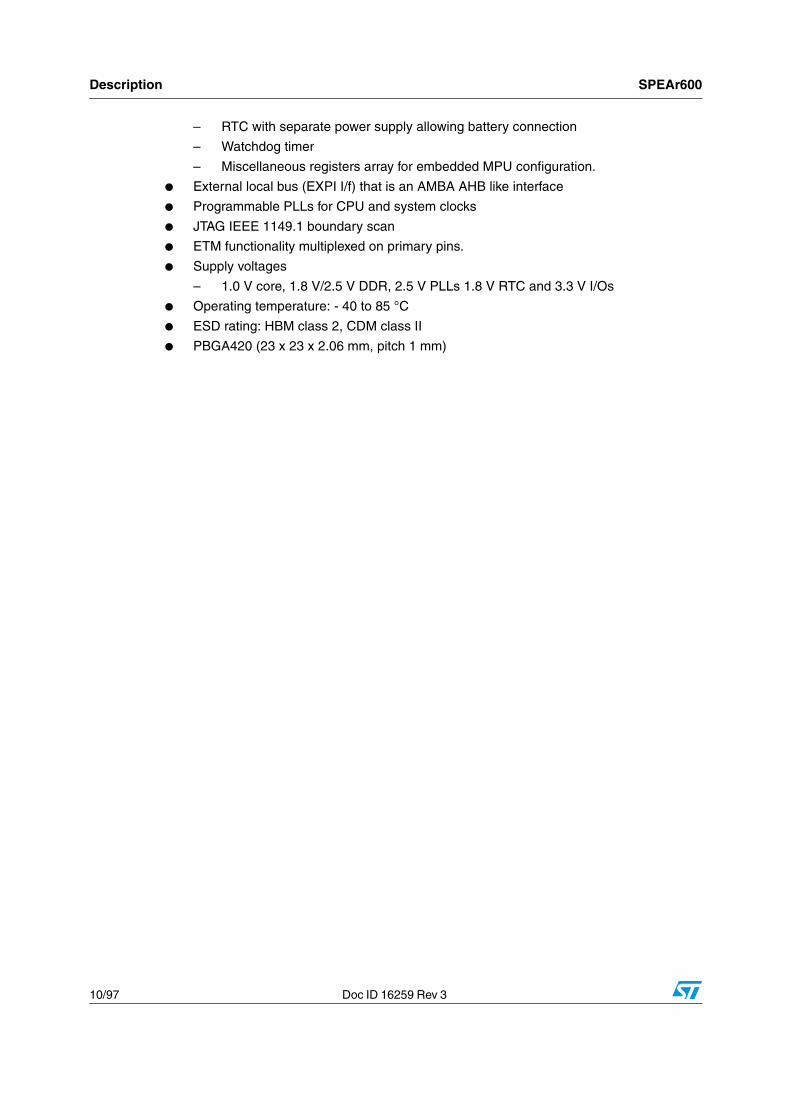
1.1 Main features● Dual core ARM926EJ-S 32-bit RISC CPU, up to 333 MHz, each with:
– 16 Kbytes of instruction cache, 16 Kbytes of data cache
– 3 instruction sets: 32-bit for high performance, 16-bit (Thumb) for efficient code density, byte Java mode (Jazelle™) for direct execution of Java code.
– Tightly Coupled Memory
– AMBA bus interface
● 32-KByte on-chip BootROM
● 8-KByte on-chip SRAM
● Dynamic memory controller managing external DDR1 memory up to 166 MHz and external DDR2 memory up to 333 MHz
● Two USB 2.0 host (high-full-low speed) with integrated PHY transceiver
● One USB 2.0 device (high-full speed) with integrated PHY transceiver
● 10 GPIO bidirectional signals with interrupt capability
● JPEG codec accelerator 1clock/pixel
● ADC 10-bit, 1 Msps 8 inputs/1-bit DAC
● 3 SSP master/slave (supporting Motorola, Texas instruments, National Semiconductor protocols) up to 40 Mbps
● I2C master/slave interface (slow/ fast/high speed, up to 1.2 Mb/s)
● 10 independent 16-bit timers with programmable prescaler
● I/O peripherals
– Two UARTs (speed rate up to 460.8 kbps)
– Fast IrDA (FIR/MIR/SIR) 9.6 Kbps to 4 Mbps speed-rate
● Audio block with 3-I2Ss interfaces to support Audio Play (Up to 3.1) and Audio Record functionality.
● Advanced power saving features
– Normal, Slow, Doze and Sleep modes, CPU clock with software-programmable frequency
– Enhanced dynamic power-domain management
– Clock gating functionality
– Low frequency operating mode
– Automatic power saving controlled from application activity demands
● Vectored interrupt controller
● System and peripheral controller
Description SPEAr600
10/97 Doc ID 16259 Rev 3
– RTC with separate power supply allowing battery connection
– Watchdog timer
– Miscellaneous registers array for embedded MPU configuration.
● External local bus (EXPI I/f) that is an AMBA AHB like interface
● Programmable PLLs for CPU and system clocks
● JTAG IEEE 1149.1 boundary scan
● ETM functionality multiplexed on primary pins.
● Supply voltages
– 1.0 V core, 1.8 V/2.5 V DDR, 2.5 V PLLs 1.8 V RTC and 3.3 V I/Os
● Operating temperature: - 40 to 85 °C
● ESD rating: HBM class 2, CDM class II
● PBGA420 (23 x 23 x 2.06 mm, pitch 1 mm)
SPEAr600 Architecture overview
Doc ID 16259 Rev 3 11/97
2 Architecture overview
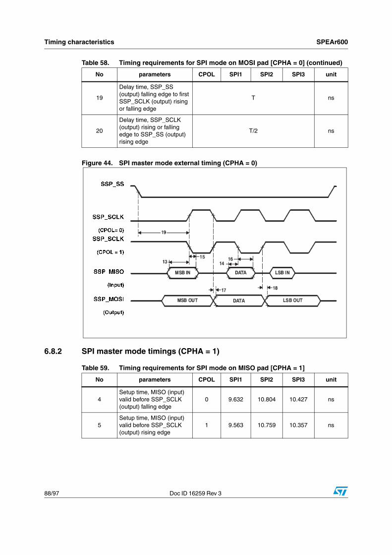
Figure 2. shows an example of a typical SPEAr600 based system.
Figure 2. Typical system architecture using SPEAr600
The core of the SPEAr600 is the dual ARM926EJ-S reduced instruction set computer (RISC) processor.
It supports the 32-bit ARM and 16-bit Thumb instruction sets, enabling the user to trade off between high performance and high code density and includes features for efficient execution of Java byte codes.
● Features a memory management unit (MMU) which makes it fully compliant with Linux and VxWorks operating systems.
The SoC includes three major subsystems logic domains which control the following function blocks:
Configurable Cell Array Subsystem
This block contains the Reconfigurable Array Subsystem logic (RAS) made by an array of 600Kgate equivalent standard cells freely customizable by means of a few metal and via mask layer changes during the customization process. The programmable logic allows reducing the SoC NRE cost, the development cycle time improving the devices time to
Clock, Reset
32 kHz30 MHz
RTC
8-Channel DMA
10 Timers / WD
8 KB Embed. SRAM
32 KB Embed. ROM
ADC
TouchScreenTouchScreen
ARM 926EJup to 333 MHz
MMUInterrupt/
Syst controller
DDR memorycontroller
DDR2DDR2
DDR1DDR1
FSMC
EEPROMEEPROM
SMIFLASHFLASH
Debug, TraceDebug, TraceJTAG
ETM9
LCD controller
USB2.0 PHYdeviceUSB2.0 PHYdevice
I2C
Internet Access
Phy
FIdDA
3xSSPUart2Uart1
USB2.0 PHYHostUSB2.0 PHYHost
USB2.0 PHYHostUSB2.0 PHYHost
ARM 926EJup to 333 MHz
MMUInterrupt/
Syst controller
3xI2SEXPI I/f
NAND FlashNAND FlashSPEAr600
RAS
Architecture overview SPEAr600
12/97 Doc ID 16259 Rev 3
market. The user custom logic can be configured using the following SoC internal resources:
● 130 Kbyte of static memory arranged in four 32 KB macro group and one 2 KB group.
● Up to 17 selectable source clocks (either internal or external)
● DMA support (up to 16 configurable dma input/output request lines)
● Power management I/F
● Interrupts line (12 outputs - 64 inputs)
● 4 AHB output master ports interconnected with the multi-channel memory controller
● 5 AHB input slave ports
● 1 interconnection port with the Expansion Interface bus (EXPI)
● 9 LVDS (8 outputs - 1 input) signals
● 88/112 PL_GPIOs primary input/output signals
Caution: PL GPIO pins are not configurable by software.
Common Subsystem
This block consists of four different logic subsystems used to control the SoC basic functions:
● I/O connectivity:
– Low speed: UARTs, SSPs, I2C and IrDA
– High speed: MII 10/100/1000, USB 2.0 host and devices
● Hardware accelerator: JPEG-codec and DMA
● Video: Color LCD interface
● Common resources: Timers, GPIOs, RTC and Watchdog
● Power management functionality
● SoC configurability: Miscellaneous control logic
CPU Subsystem
The SPEAr600 has a symmetric processor architecture with:
● 2 equivalent subsystems including the ARM926 and its private subsystem logic (GPIOs, Interrupt controller and Timer) providing the essential hardware resources to support a generic Operating System
● The subsystem is replicated twice so both processors have the same memory map. This structure enables a true symmetric multi-processor architecture were both processors can simultaneously execute the same OS (all interrupt sources are handled by both processors)
● All internal peripherals are shared, allowing flexible and efficient software partitions.
● High aggregate throughput can be sustained by splitting critical tasks either onto additional CPUs and optional hardware accelerator engines.
● Both processors are equipped with ICE and ETM configurable debug interfaces. for real-time CPU activity tracing and debugging. 4-bit and 8-bit normal trace mode and 4-bit demultiplexed trace mode is supported, with normal or half-rate clock.
The internal architecture is also based on several shared subsystem logic blocks interconnected through a multilayer interconnection matrix. The switch matrix structure
SPEAr600 Architecture overview
Doc ID 16259 Rev 3 13/97
allows different subsystem data flows to be executed in parallel improving the core platform efficiency.
High performance master agents are directly interconnected with the memory controller reducing the memory access latency. The overall memory bandwidth assigned to each master port can be programmed and optimized through an internal efficient weighted round-robin arbitration mechanism.
2.1 Embedded memory unitsThe SPEAr600 has two embedded memory units
● 32 Kbytes of BootROM
● 8 Kbytes of SRAM
2.2 DDR/DDR2 memory controllerSPEAr600 integrates a high performance multi-channel memory controller able to support DDR1 and DDR2 double data rate memory devices. The multi-port architecture ensures that memory is shared efficiently among different high-bandwidth client modules.
Main features:
● Multi channel AHB interfaces:
– Seven independent AHB ports
– Separate AHB memory controller programming interface
– Support all AHB burst types
– Lock transaction are not supported
● Internal efficient port arbitration scheme to ensure high memory bandwidth utilization
● Programmable register interface to control memory device parameters and protocols
● DRAM controller supports both DDR1 and DDR2 memory devices:
– DDR1 up to 166 MHz
– DDR2 up to 333 MHz
● Memory frequency with DLL enable configurable from 100 MHz to 333 MHz
● Wide range of memory devices supported:
– 128 Mbit, 256 Mbit, 512 Mbit, 1 Gbit, 2 Gbit
– Two chip selects.
– 8 or 16-bit data width
2.3 Serial memory interfaceSPEAr600 provides a Serial Memory Interface (SMI), acting as an AHB slave interface (32-, 16- or 8-bit) to SPI-compatible off-chip memories.
These serial memories can be used either as data storage or for code execution.
Architecture overview SPEAr600
14/97 Doc ID 16259 Rev 3
Main features:
● Supports the following SPI-compatible Flash and EEPROM devices:
– STMicroelectronics M25Pxxx, M45Pxxx
– STMicroelectronics M95xxx, except M95040, M95020 and M95010
– ATMEL AT25Fxx
– YMC Y25Fxx
– SST SST25LFxx
● Acts always as a SPI master and supports up to 3 SPI slave memory devices (with separate chip select signals), with up to 16 MB address space each
● SMI clock (SMICLK) is generated by SMI (and input to all slaves) using a clock provided by the AHB bus
● SMI_CLK can be up to 50 MHz in fast read mode (or 20 MHz in normal mode). It can be controlled by 7 programmable bits.
2.4 Flexible static memory controllerRoot part number 1 provides Flash Nand Static Memory Controller (FSMC) which is intended to interface an AHB bus to external NAND Flash memories.
Main purpose of FSMC is then:
● Translate AHB protocol into the appropriate external storage device protocol
● Meet the timing of the external devices, slowing down and counting an appropriate number of HCLK (AHB clock) cycles to complete the transaction to the external device
Note: The external storage device cannot be faster than one AHB cycle.
Main features of the FSMC are listed below:
● The FSMC is an AMBA slave module connected to the AHB
● Provides an interface between AHB system bus and Nand Flash memory devices with 8 and 16 bits wide data paths
● FSMC performs only one access at a time and only one external device is accessed
● Support little-endian and big-endian memory architectures
● Handles AHB burst transfers to reduce access time to external devices
● Supplies an independent configuration for each memory bank
● Provides programmable timings to support a wide range of devices:
– Programmable wait states (up to 31)
– Programmable bus turn around cycles (up to 15)
– Programmable output enable and write enable delays (up to 15)
● Provides only one chip select for the first memory bank
● Shares the address bus and the data bus with all the external peripherals, whereas only chips selects are unique for each peripheral
● Offers an external asynchronous wait control
● Offers configurable size at reset for boot memory bank using external control pins.
SPEAr600 Architecture overview
Doc ID 16259 Rev 3 15/97
2.5 Multichannel DMA controllerWithin its basic subsystem, SPEAr600 provides a DMA controller (DMAC) able to service up to 8 independent DMA channels for serial data transfers between a single source and destination (i.e., memory-to-memory, memory-to-peripheral, peripheral to-memory, and peripheral-to-peripheral).
Each DMA channel can support unidirectional transfers, with one internal four-word FIFO per channel.
2.6 LCD controllerMain features:
● Resolution programmable up to 1024 x 768
● 16-bpp true-color non-palletized, for color STN and TFT
● 24-bpp true-color non-palletized, for color TFT
● Supports single and dual panel mono super twisted nematic (STN) displays with 4 or 8-bit interfaces
● Supports single and dual-panel color and monochrome STN displays
● Supports thin film transistor (TFT) color displays
● 15 gray-level mono, 3375 color STN, and 32 K color TFT support
● 1, 2, or 4 bits per pixel (bpp) palletized displays for mono STN
● 1, 2, 4 or 8-bpp palletized color displays for color STN and TFT
● Programmable timing for different display panels
● 256 entry, 16-bit palette RAM, arranged as a 128 x 32-bit RAM physically frame, line and pixel clock signals
● AC bias signal for STN and data enable signal for TFT panels patented gray scale algorithm
● Supports little-endian, big-endian and WinCE data formats
2.7 GPIOsThe General Purpose Input/Outputs (GPIOs) provide programmable inputs or outputs.
Each input/output can be controlled in two distinct modes:
● Software mode, through an APB interface
● Hardware mode, through a hardware control interface.
SPEAr600 provides up to 10 GPIO lines:
● Individually programmable input/output pins (default to input at reset)
● An APB slave acting as control interface in "software mode"
● Programmable interrupt generation capability on any number of pins
● Bit masking in both read and write operations through address lines
Architecture overview SPEAr600
16/97 Doc ID 16259 Rev 3
2.8 JPEG codecMain features:
● Compliance with the baseline JPEG standard (ISO/IEC 10918-1)
● Single-clock per pixel encoding/decoding
● Support for up to four channels of component color
● 8-bit/channel pixel depths
● Programmable quantization tables (up to four)
● Programmable Huffman tables (two AC and two DC)
● Programmable minimum coded unit (MCU)
● Configurable JPEG headers processing
● Support for restart marker insertion
● Use of two DMA channels and of two 8 x 32-bits FIFOs (local to the JPEG) for efficient transferring and buffering of encoded/decoded data from/to the codec core.
2.9 8-channel ADCMain features:
● Successive approximation ADC
● 10-bit resolution @1 Msps
● Hardware over sampling and accumulation up to 128 samples
● Eight analog input (AIN) channels, ranging from 0 to 2.5 V
● INL ± 1 LSB, DNL ± 1 LSB
● Programmable conversion speed, (min. conversion time is 1 µs)
● Programmable averaging of results from 1 (No averaging) up to 128
2.10 Ethernet controllerMain features:
● Supports the default Gigabit Media Independent Interface (GMII)/Media Independent Interface (MII) defined in the IEEE 802.3 specifications.
● Supports 10/100/1000 Mbps data transfer rates with any one or a combination of the above PHY interfaces
● Supports both half-duplex and full-duplex operation. In half-duplex operation, CSMA/CD protocol is provided for, as well as packet bursting and frame extension at 1000 Mbps
● Programmable frame length to support both Standard and Jumbo Ethernet frames with size up to 16 Kbytes
● 32-bit data transfer interface on system-side
● A variety of flexible address filtering modes are supported
● A set of control and status registers (CSRs) to control GMAC Core operation.
● Complete network statistics with RMON Counters (MMC, MAC Management Counters).
SPEAr600 Architecture overview
Doc ID 16259 Rev 3 17/97
● Native DMA with single-channel Transmit and Receive engines, providing 32/64/128-bit data transfers
● DMA implements dual-buffer (ring) or linked-list (chained) descriptor chaining
● A set of CSRs to control DMA operation
● An AHB slave acting as programming interface to access all CSRs, for both DMA and GMAC core subsystems
● An AHB master for data transfer to system memory
● 32-bit AHB master bus width, supporting 32-bit wide data transactions
● Supports both big-endian and little-endian byte ordering
● Power Management Module (PMT) with Remote Wake-up and Magic Packet frame processing options
2.11 USB2 host controllerSPEAr600 has two fully independent USB 2.0 hosts. Each consists of 5 major blocks:
● OHCI that manages the full and the low speed transfers (12 and 1.5 Mbps)
● Local 2-Kbyte FIFO
● Local DMA
● Integrated USB2 transceiver (PHY)
Both hosts can manage an external power switch, providing a control line to enable or disable the power, and an input line to sense any over-current condition detected by the external switch.
Both host controllers can perform high speed transfer simultaneously.
2.12 USB2 device controllerMain features:
● Supports 480 Mbps high-speed mode (HS) for USB 2.0, as well as 12 Mbps full-speed (FS) and the low-speed (LS modes) for USB 1.1
● Supports 16 physical endpoints, which can be assigned to different interfaces and configurations to implement logical endpoints
● Integrated USB transceiver (PHY)
● Local 4 Kbyte FIFO shared by all endpoints
● DMA mode and slave-only mode are supported
● In DMA mode, the UDC supports descriptor-based memory structures in application memory
● In both modes, an AHB slave is provided by UDC-AHB, acting as programming interface to access to memory-mapped control and status registers (CSRs)
● An AHB master for data transfer to system memory is provided, supporting 8, 16, and 32-bit wide data transactions on the AHB bus
● A USB plug detect (UPD) which detects the connection of a cable.
Architecture overview SPEAr600
18/97 Doc ID 16259 Rev 3
2.13 Synchronous Serial Peripheral (SSP)The SPEAR600 has three Synchronous Serial Peripherals (SSPs) (SPI, Microwire or TI protocol).
Main features:
● Maximum speed of 40 Mbps
● Programmable choice of interface protocol:
– SPI (Motorola)
– Microwire (National Semiconductor)
– TI synchronous serial
● Programmable data frame size from 4 to 16-bit.
● Master and slave mode capability.
● DMA interface
2.14 I2CMain features:
● Compliance to the I2C bus specification (Philips)
● I2C v2.0 compatible.
● Supports three modes:
– Standard (100 kbps)
– Fast (400 kbps)
– High-speed (3.4 Mbps)
● Master and slave mode configuration possible
● Slave Bulk data transfer capability
● DMA interface
2.15 UARTsThe SPEAr600 has two UARTs.
Main features:
● Hardware flow control
● Separate 16x8 (16 locations deep x 8 bits wide) transmit and 16 x 12 receive FIFOs to reduce CPU interrupts
● Speed up to 3 Mbps
SPEAr600 Architecture overview
Doc ID 16259 Rev 3 19/97
2.16 Fast IrDA controllerThe SPEAr600 has a Fast IrDA controller.
Main features:
● Supports the following standards:
– IrDA serial infrared physical layer specification (IrPHY), version 1.3
– IrDA link access protocol (IrLAP), version 1.1
● Supports the following infrared modes and baud rates:
– Serial infrared (SIR), with rates 9.6 kbps, 19.2 kbps, 38.4 kbps, 57.6 kbps and 115.2 kbps
– Medium Infrared (MIR), with rates 576 kbps and 1.152 Mbps
– Fast Infrared (FIR), with rate 4 Mbps
● Transceiver interface compliant to all IrDA transceivers with configurable TX and RX signal polarity
● Half-duplex infrared frame transmission and reception
● 16-bit CRC algorithm for SIR and MIR, and 32-bit CRC algorithm for FIR
● Generates preamble, start and stop flags
● Uses the RZI (Return-to-Zero Inverted) modulation/demodulation scheme for SIR and MIR, and the 4PPM (4 Pulse Position Modulation) modulation/demodulation scheme for FIR
● Provides synchronization by means of a DPLL in FIR mode
● Easily adaptable to different bus systems with 32-bit register interface and FIFO with configurable FIFO size
2.17 I2S audio blockSPEAr600 contains three I2S interfaces providing the following features.
Main features:
● Conversion of AHB protocol to I2S protocol and vice versa
2.18 System controllerThe System Controller provides an interface for controlling the operation of the overall system.
Main features:
● Power saving system mode control
● Crystal oscillator and PLL control
● Configuration of system response to interrupts
Architecture overview SPEAr600
20/97 Doc ID 16259 Rev 3
● Reset status capture and soft reset generation
● Watchdog module clock enable
2.18.1 Power saving system mode control
Using three mode control bits, the system controller switch the SPEAr600 to any one of four different modes: DOZE, SLEEP, SLOW and NORMAL.
● SLEEP mode: In this mode the system clocks, HCLK and CLK, are disabled and the System Controller clock SCLK is driven by a low speed oscillator (nominally 32768 Hz). When either a FIQ or an IRQ interrupt is generated (through the VIC) the system enters DOZE mode. Additionally, the operating mode setting in the system control register automatically changes from SLEEP to DOZE.
● DOZE mode: In this mode the system clocks, HCLK and CLK, and the System Controller clock SCLK are driven by a low speed oscillator. The System Controller moves into SLEEP mode from DOZE mode only when none of the mode control bits are set and the processor is in Wait-for-interrupt state. If SLOW mode or NORMAL mode is required the system moves into the XTAL control transition state to initialize the crystal oscillator.
● SLOW mode: During this mode, both the system clocks and the System Controller clock are driven by the crystal oscillator. If NORMAL mode is selected, the system goes into the "PLL control" transition state. If neither the SLOW nor the NORMAL mode control bits are set, the system goes into the "Switch from XTAL" transition state.
● NORMAL mode: In NORMAL mode, both the system clocks and the System Controller clock are driven by the PLL output. If the NORMAL mode control bit is not set, then the system goes into the "Switch from PLL" transition state.
2.19 Clock and reset systemThe clock system is a fully programmable block that generates all the clocks for the SPEAr600.
The default operating clock frequencies are:
● Clock @ 333 MHz for the CPUs.
● Clock @ 166 MHz for AHB bus and AHB peripherals. (PLL1 source)
● Clock @ 83 MHz for, APB bus and APB peripherals. (PLL1 source)
● Clock @ 12 MHz, 30 MHz and 48 MHz for USBs (PLL3 source)
The above frequencies are the maximum allowed values.
All these clocks are generated by three PLLs.
PLL1 and PLL2 sources are fully programmable through dedicated registers.
The clock system consists of 2 main parts: a multi clock generator block and two internal PLLs.
The multi clock generator block, takes a reference signal (which is usually delivered by the PLL), generates all clocks for the IPs of SPEAr600 according to dedicated programmable registers.
SPEAr600 Architecture overview
Doc ID 16259 Rev 3 21/97
Each PLL uses an oscillator input of 30 MHz to generate a clock signal at a frequency corresponding to the highest of the group. This is the reference signal used by the multi clock generator block to obtain all the other required clocks for the group. Its main feature is electromagnetic interference reduction capability.
The user can set up the PLL in order to modulate the VCO with a triangular wave. The resulting signal has a spectrum (and power) spread over a small programmable range of frequencies centered on F0 (the VCO frequency), obtaining minimum electromagnetic emissions. This method replaces all the other traditional methods of EMI reduction, such as filtering, ferrite beads, chokes, adding power layers and ground planes to PCBs, metal shielding and so on. This gives the customer appreciable cost savings.
In sleep mode the SPEAr600 runs with the PLL disabled so the available frequency is 30 MHz or a sub-multiple (/2, /4, /16 and /32) or 32 KHz.
PLL3 is used to generate the USB controller clocks and it is not configured through registers.
2.20 Vectored interrupt controller (VIC)Each ARM Subsystem of SPEAr600 offers Vectored Interrupted Controller (VIC) blocks, providing a software interface to the interrupt system.
Acting as an interrupt controller, the VIC determines the source that is requesting service and where its interrupt service routine (ISR) is loaded, doing that in hardware.
In particular, the VIC supplies the starting address, or vector address, of the ISR corresponding to the highest priority requesting interrupt source.
Main features of the VIC are listed below:
● Support for 32 standard interrupt sources (a total of 64 lines are available for each CPU from its two daisy-chained VICs).
● Generation of both Fast Interrupt request (FIQ) and Interrupt Request (IRQ. IRQ is used for general interrupts, whereas FIQ is intended for fast, low-latency interrupt handling.
● Support for 16 vectored interrupts (IRQ only);
● Hardware interrupt priority
– FIQ interrupt has the highest priority
– followed by vectored IRQ interrupts, from vector 0 to vector 15
– then non-vectored IRQ interrupts with the lowest priority
● Interrupt masking/ interrupts request status
● Software interrupt generation
2.21 General purpose timersSPEAr600 provides five general purpose timers (GPTs) acting as APB slaves.
Each GPT consists of 2 channels, each one made up of a programmable 16-bit counter and a dedicated 8-bit timer clock prescaler. The programmable 8-bit prescaler performs a clock division by 1 up to 256, and different input frequencies can be chosen through SPEAr600 configuration registers (frequencies up to 83 MHz can be synthesized).
Architecture overview SPEAr600
22/97 Doc ID 16259 Rev 3
Two different modes of operation are available:
● Auto-reload mode, an interrupt source is activated, the counter is automatically cleared and then it restarts incrementing.
● Single-shot mode, an interrupt source is activated, the counter is stopped and the GPT is disabled.
2.22 Watchdog timerThe ARM watchdog module consists of a 32-bit down counter with a programmable time-out interval that has the capability to generate an interrupt and a reset signal on timing out. The watchdog module is intended to be used to apply a reset to a system in the event of a software failure.
2.23 RTC oscillatorThe RTC provides a 1-second resolution clock. This keeps time when the system is inactive and can be used to wake the system up when a programmed alarm time is reached. It has a clock trimming feature to compensate for the accuracy of the 32.768 kHz crystal and a secured time update.
Main features:
● Time-of-day clock in 24 hour mode
● Calendar
● Alarm capability
● Isolation mode, allowing RTC to work even if power is not supplied to the rest of the device.
2.24 Reconfigurable array subsystem connectivity (RAS)The Reconfigurable Logic Array consists of an embedded macro where it is possible to implement a custom project by mapping up to 600k equivalent standard cells. The user can design custom logic and special function using various features offered by the Reconfigurable Logic Array and by the SPEAr600 system listed here below.
● 4 AHB bus master interfaces
● 5 AHB bus slave interfaces
● Dedicated interface with CPU1 to customize the Tightly Couple Memory
● Dedicated interface with CPU1 to customize the Coprocessor
● Dedicated interface with CPU2 to customize the Tightly Coupled Memory
● Interfaces towards a dedicated 130 kB Memory Array Subsystem provided of functional BIST driven by SoC via software and divided in the following ST memory cuts:
– 3 single port memory cuts (48 words x 128 bits)
– 4 single port memory cuts (2048 words x 32 bits)
– 8 single port memory cuts (1024 words x 32 bits)
– 16 single port memory cuts (512 words x 32 bits)
– 8 dual port memory cuts (512 words x 32 bits)
SPEAr600 Architecture overview
Doc ID 16259 Rev 3 23/97
– 4 dual port memory cuts (1024 words x 32 bits)
● Clock system constituted by:
– 5 clocks coming from the external balls
– 4 clocks coming from the integrated frequency synthesizers
– CPU core clock frequency
– Pll2 frequency
– 48 MHz clock (USB Pll)
– 30 MHz clock (Main Oscillator)
– 32.768 kHz clock (RTC Oscillator)
– APB clock (programmable)
– AHB clock (programmable)
– User Configurable sync/async clock towards Memory Controller port 2 (M2)
● Connection with 84/112 I/Os
● Connection with 9 LVDS lines
● 12 interrupt lines towards CPU1 and CPU2
● 64 interrupt input lines from the various platform IP sources
● 16 peripheral DMA request lines
● 64 user configurable (in the SoC) general purpose input lines
● 64 user configurable (in the RAS) general purpose output lines
● SoC dynamic power management control interface;
● 50 specific ATE Test interface signals dedicated to RAS
2.25 External Port Controller (EXPI I/F)The port controller is a socket communication interface between the SPEAr600 and an external FPGA device; it implements a simple AHB bidirectional protocol used to compress a couple of std AHB master/slave bus onto 84 PL_GPIOs and 4 PL_CLK primary signals.
Caution: PL_GPIO pins are not configurable by software.
ST provide a symmetric port controller logic solution to be embedded inside the external FPGA with the purpose of interfacing the EXPI bus directly and decompressing the same pair of AHB master/slave ports on the FPGA side in order to interconnect the customer logic as follows (more slave and master agents can be connected to the EXPI):
SPEAr600_AHB-master >> FPGA_AHB-slave
SPEAr600_AHB-slave << FPGA_AHB-master (AHB-full)
The EXPI interface is based on two main groups of signals:
● AHB bidirectional signal bus driven alternatively from the SPEAr600 and FPGA side.
● Unidirectional signals continuously driven from both the SPEAr600 and FPGA sides.
Table 36: EXPI - pad signal assignment lists the EXPI signal names. Further details in these signals are given in the SPEAr600 user manual (UM0510)
Pin description SPEAr600
24/97 Doc ID 16259 Rev 3
3 Pin description
The following tables describe the pinout of the SPEAr600 listed by functional block.
This description refers to the default configuration of SPEAr600 (full features).
More details on the configuration of each pin are given in Table 16: Multiplexing scheme.
● Table 2: System reset, master clock, RTC and configuration pins
● Table 3: Power supply pins
● Table 4: Debug pins
● Table 5: SMI, SSP, UART, FIRDA and I2C pins
● Table 6: USB pins
● Table 7: Ethernet pins
● Table 8: GPIO pins
● Table 9: ADC pins
● Table 10: NAND Flash I/F pins
● Table 11: DDR I/F pins
● Table 12: LCD I/F pins
● Table 13: LVDS I/F pins
● Table 14: EXPI/I2S pins
● Table 15: EXPI pins
List of abbreviations:
PU = Pull Up
PD = Pull Down
3.1 Required external components1. DDR_COMP_1V8: place an external 121 kΩ resistor between ball V7 and ball V8
2. DDR_COMP_2V5: place an external 121 kΩ resistor between ball V9 and ball V8
3. USB_RREF: connect an external 1.5 kΩ pull-down resistor to ball U4
4. DIGITAL_REXT: place an external 121 kΩ resistor between ball E11 and ball E126.
3.2 Pin descriptions listed by functional block
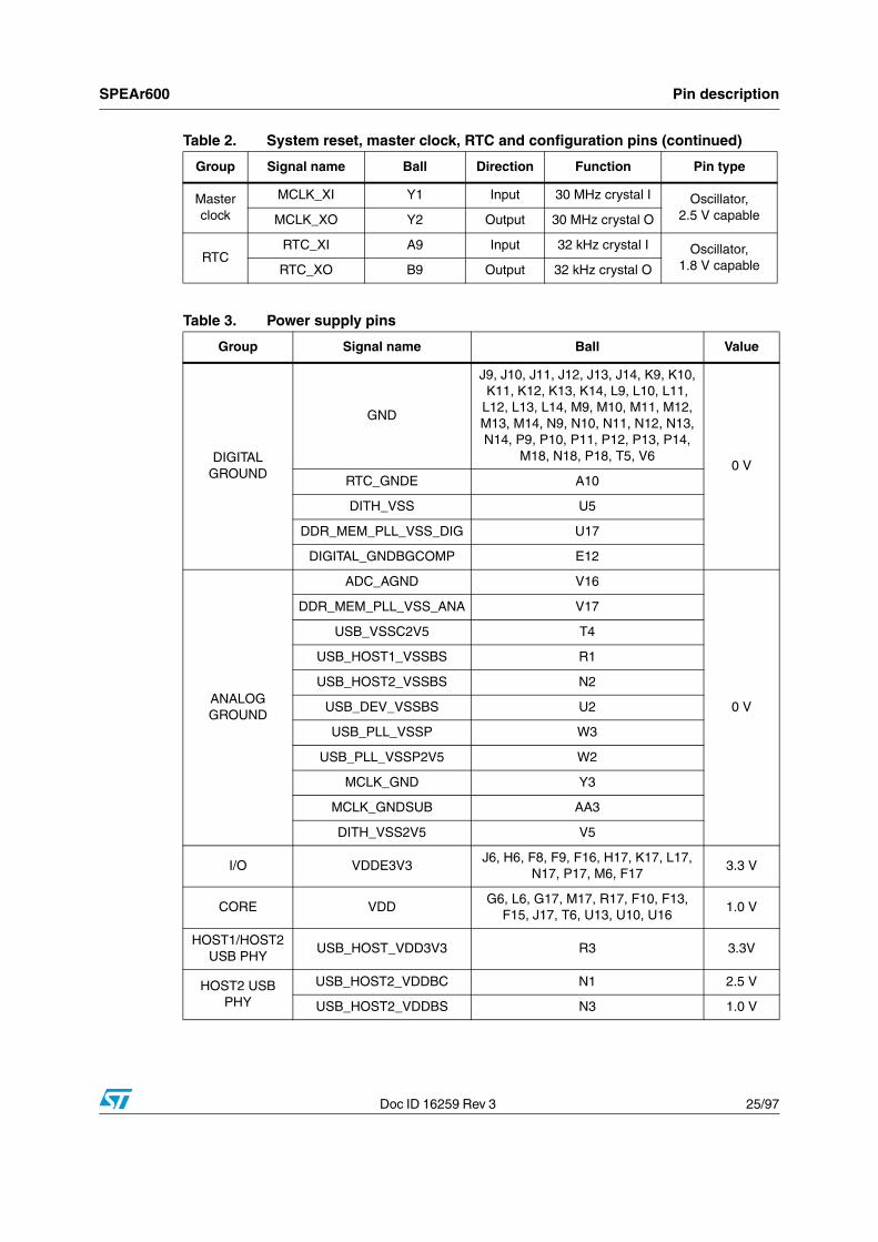
Table 2. System reset, master clock, RTC and configuration pins
Group Signal name Ball Direction Function Pin type
SYSTEM RESET
MRESET C17 Input Main reset
TTL Schmitt trigger input
buffer,3.3 V tolerant, PU
CONFIG DIGITAL_REXT E11 Ref ConfigurationAnalog,
3.3 V capable, See Note 4
SPEAr600 Pin description
Doc ID 16259 Rev 3 25/97
Master clock
MCLK_XI Y1 Input 30 MHz crystal I Oscillator, 2.5 V capableMCLK_XO Y2 Output 30 MHz crystal O
NF_RB H22 Input Read/busy TTL input buffer 3.3 V tolerant, PU
SPEAr600 Pin description
Doc ID 16259 Rev 3 33/97
Table 11. DDR I/F pins
Group Signal name Ball Direction Function Pin type
DDRI/F
DDR_ADD_0 AB3
OutputAddress
line
SSTL_2/SSTTL_18
DDR_ADD_1 AB4
DDR_ADD_2 AA4
DDR_ADD_3 Y4
DDR_ADD_4 W4
DDR_ADD_5 W5
DDR_ADD_6 Y5
DDR_ADD_7 AA5
DDR_ADD_8 AB5
DDR_ADD_9 AB6
DDR_ADD_10 AA6
DDR_ADD_11 Y6
DDR_ADD_12 W6
DDR_ADD_13 W7
DDR_ADD_14 Y7
DDR_BA_0 Y9
OutputBank
selectDDR_BA_1 W9
DDR_BA_2 W10
DDR_RAS AB7
Output
Row strobe
DDR_CAS AA7 Column strobe
DDR_WE AA8 Write enable
DDR_CLKEN AB8 Clock enable
DDR_CLK_P AA9Output
Differential Differential
DDR_CLK_N AB9 Clock SSTL_2/ SSTTL_18
DDR_CS_0 Y8Output
Chip select
SSTL_2/ SSTTL_18
DDR_CS_1 W8 Chip select
DDR_ODT_0 AB2Output
On-die Termination
DDR_ODT_1 AB1 Enable lines
DDR_DATA_0 AB11
I/OData lines
(lower byte)
DDR_DATA_1 AA10
DDR_DATA_2 AB10
DDR_DATA_3 Y10
DDR_DATA_4 Y11
Pin description SPEAr600
34/97 Doc ID 16259 Rev 3
DDR
I/F
DDR_DATA_5 Y12Data lines
(Lower byte)SSTL_2
/SSTTL_18DDR_DATA_6 AB12
DDR_DATA_7 AA12
DDR_DQS_0 AB13I/O
Differential lower
Data Strobe
Differential
SSTL_2/ SSTTL_18DDR_nDQS_0 AA13
DDR_DM_0 AA11 OutputLower data
mask
SSTL_2/ SSTTL_18
DDR_GATE_0 Y13 I/O Lower gate open
DDR_DATA_8 AB15
I/OData lines
(Upper byte)
DDR_DATA_9 AA16
DDR_DATA_10 AB16
DDR_DATA_11 Y16
DDR_DATA_12 Y15
DDR_DATA_13 Y14
DDR_DATA_14 AB14
DDR_DATA_15 AA14
DDR_DQS_1 AB17 I/ODifferential
upperDifferential
DDR_nDQS_1 AA17 Data strobeSSTL_2/
SSTTL_18
DDR_DM_1 AA15 OutputUpper data
mask SSTL_2/ SSTTL_18
DDR_GATE_1 Y17 I/OUpper gate
open
DDR_VREF V10 Input Ref. voltage Analog
DDR_COMP_2V5 V9 Ref Ext. ref resistorAnalog, see Note 2 on page 24
DDR_COMP_GND
V8 -Common return for Ext. resistors
Power
DDR_COMP_1V8 V7 Ref Ext. ref. resistorAnalog, see Note 1 on page 24
DDR2_EN D11 Input ConfigurationTTL input buffer,
3.3 V tolerant, PU
Table 11. DDR I/F pins (continued)
Group Signal name Ball Direction Function Pin type
SPEAr600 Pin description
Doc ID 16259 Rev 3 35/97
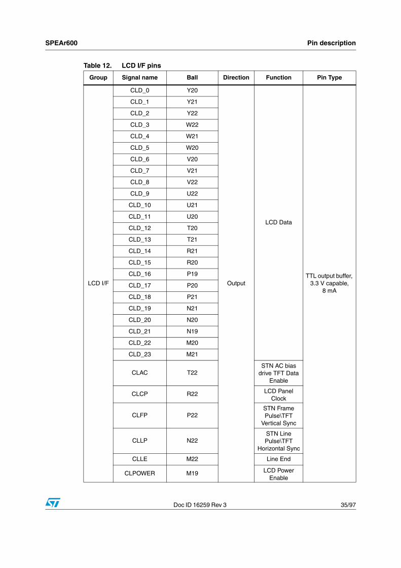
Table 12. LCD I/F pins
Group Signal name Ball Direction Function Pin Type
LCD I/F
CLD_0 Y20
Output
LCD Data
TTL output buffer, 3.3 V capable,
8 mA
CLD_1 Y21
CLD_2 Y22
CLD_3 W22
CLD_4 W21
CLD_5 W20
CLD_6 V20
CLD_7 V21
CLD_8 V22
CLD_9 U22
CLD_10 U21
CLD_11 U20
CLD_12 T20
CLD_13 T21
CLD_14 R21
CLD_15 R20
CLD_16 P19
CLD_17 P20
CLD_18 P21
CLD_19 N21
CLD_20 N20
CLD_21 N19
CLD_22 M20
CLD_23 M21
CLAC T22STN AC bias
drive TFT Data Enable
CLCP R22 LCD Panel Clock
CLFP P22STN Frame Pulse\TFT
Vertical Sync
CLLP N22STN Line Pulse\TFT
Horizontal Sync
CLLE M22 Line End
CLPOWER M19 LCD Power Enable
Pin description SPEAr600
36/97 Doc ID 16259 Rev 3
Table 13. LVDS I/F pins
Group Signal name Ball Direction Function Pin Type
LVDS I/F
PH0 A16
Output General purpose I/O With LVDS transceiver
LVDS Driver
PH0n B16
PH1 C16
PH1n C15
PH2 A15
PH2n B15
PH3 A14
PH3n B14
PH4 C14
PH4n C13
PH5 A13
PH5n B13
PH6 A12
PH6n B12
PH7 C12
PH7n C11
PH8 A11Input LVDS Receiver
PH8n B11
SPEAr600 Pin description
Doc ID 16259 Rev 3 37/97
Table 14. EXPI/I2S pins
Group Signal name Ball Direction Function Pin Type
EXPI/I2S
PL_GPIO_47/ADO_REC_DIN
C2
I/O Logic I/O
TTL bidirectional buffer
3.3 V capable,3.3 V tolerant,
4 mA,PU(1)
1. When the pin is not driven, the output voltage is 2.5 V, On the core side, logic ‘1’ state is guaranteed.
PL_GPIO_48/ADO_REC_WS
C1
PL_GPIO_50/ADO_WS_OUT
A1
PL_GPIO_51/ADO_DOUT2
B2
PL_GPIO_52/ADO_DOUT1
A2
PL_GPIO_53/ADO_CLK_in_529
C3
PL_GPIO_54/
MCLK_out_309B3
PL_GPIO_55/
ADO_RECORD_CLKA3
PL_CLK_4/
ADO_CLK_OUTA4 Output
Logic External Clock
TTL bidirectional buffer, 3.3 V
capable, 8 mA, 3.3 V tolerant,
PU(1)
Pin description SPEAr600
38/97 Doc ID 16259 Rev 3
Table 15. EXPI pins
Group Signal name Ball Direction Function Pin Type
EXPI
PL_GPIO_0 P4
I/O Logic I/O
TTL bidirectional buffer
3.3 V capable,
3.3 V tolerant, 4 mA,
PU(1)
PL_GPIO_1 N4
PL_GPIO_2 N5
PL_GPIO_3 N6
PL_GPIO_4 M5
PL_GPIO_5 M4
PL_GPIO_6 M3
PL_GPIO_7 M2
PL_GPIO_8 M1
PL_GPIO_9 L1
PL_GPIO_10 L2
PL_GPIO_11 L3
PL_GPIO_12 L4
PL_GPIO_13 L5
PL_GPIO_14 K6
PL_GPIO_15 K5
PL_GPIO_16 K4
PL_GPIO_17 K3
PL_GPIO_18 K2
PL_GPIO_19 K1
PL_GPIO_20 J1
PL_GPIO_21 J2
PL_GPIO_22 J3
PL_GPIO_23 J4
PL_GPIO_24 J5
PL_GPIO_25 H5
PL_GPIO_26 H4
PL_GPIO_27 H3
PL_GPIO_28 H2
PL_GPIO_29 H1
PL_GPIO_30 G1
PL_GPIO_31 G2
SPEAr600 Pin description
Doc ID 16259 Rev 3 39/97
EXPI
PL_GPIO_32 G3
I/O Logic I/O
TTL bidirectional buffer
3.3 V capable, 4 mA,
3.3 V tolerant, PU(1)
PL_GPIO_33 G4
PL_GPIO_34 G5
PL_GPIO_35 F5
PL_GPIO_36 F4
PL_GPIO_37 F3
PL_GPIO_38 F2
PL_GPIO_39 F1
PL_GPIO_40 E4
PL_GPIO_41 E3
PL_GPIO_42 E2
PL_GPIO_43 E1
PL_GPIO_44 D3
PL_GPIO_45 D2
PL_GPIO_46 D1
PL_GPIO_49 B1
PL_GPIO_56 B4
PL_GPIO_57 C4
PL_GPIO_58 D4
PL_GPIO_59 E5
PL_GPIO_60 D5
PL_GPIO_61 C5
PL_GPIO_62 B5
PL_GPIO_63 B6
Table 15. EXPI pins (continued)
Group Signal name Ball Direction Function Pin Type
Pin description SPEAr600
40/97 Doc ID 16259 Rev 3
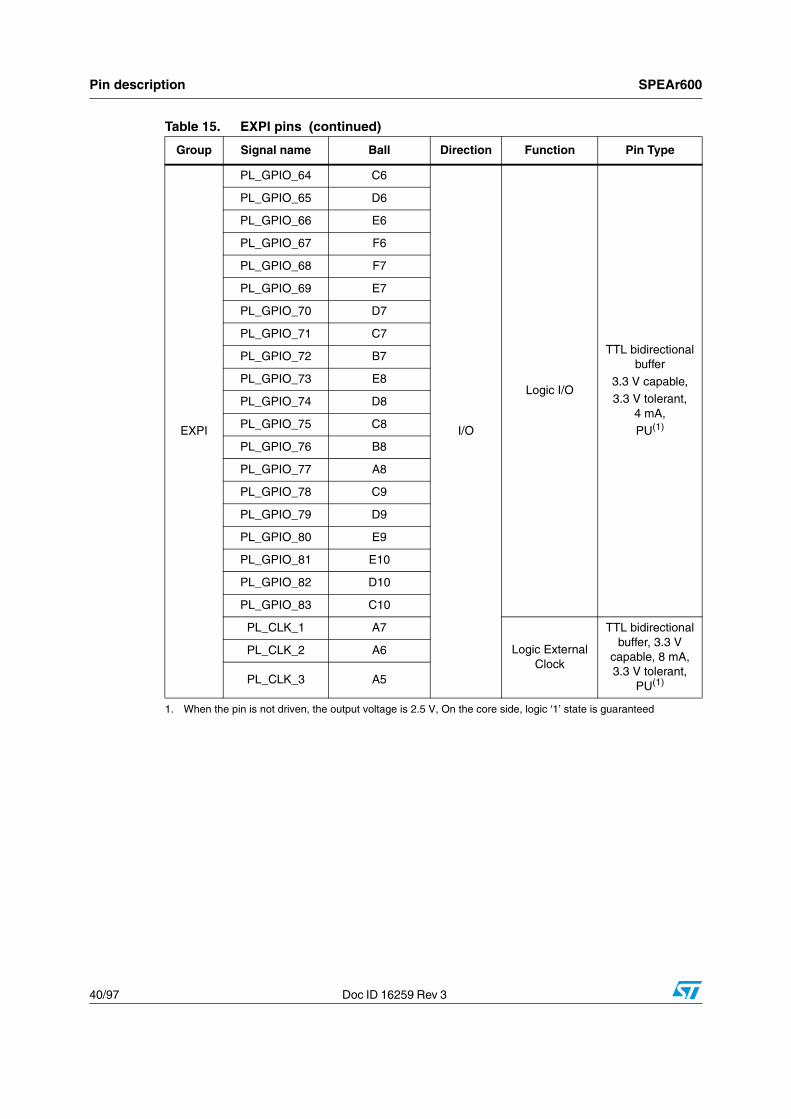
EXPI
PL_GPIO_64 C6
I/O
Logic I/O
TTL bidirectional buffer
3.3 V capable, 3.3 V tolerant,
4 mA,
PU(1)
PL_GPIO_65 D6
PL_GPIO_66 E6
PL_GPIO_67 F6
PL_GPIO_68 F7
PL_GPIO_69 E7
PL_GPIO_70 D7
PL_GPIO_71 C7
PL_GPIO_72 B7
PL_GPIO_73 E8
PL_GPIO_74 D8
PL_GPIO_75 C8
PL_GPIO_76 B8
PL_GPIO_77 A8
PL_GPIO_78 C9
PL_GPIO_79 D9
PL_GPIO_80 E9
PL_GPIO_81 E10
PL_GPIO_82 D10
PL_GPIO_83 C10
PL_CLK_1 A7
Logic External Clock
TTL bidirectional buffer, 3.3 V
capable, 8 mA, 3.3 V tolerant,
PU(1)
PL_CLK_2 A6
PL_CLK_3 A5
1. When the pin is not driven, the output voltage is 2.5 V, On the core side, logic ‘1’ state is guaranteed
Table 15. EXPI pins (continued)
Group Signal name Ball Direction Function Pin Type
SPEAr600 Pin description
Doc ID 16259 Rev 3 41/97
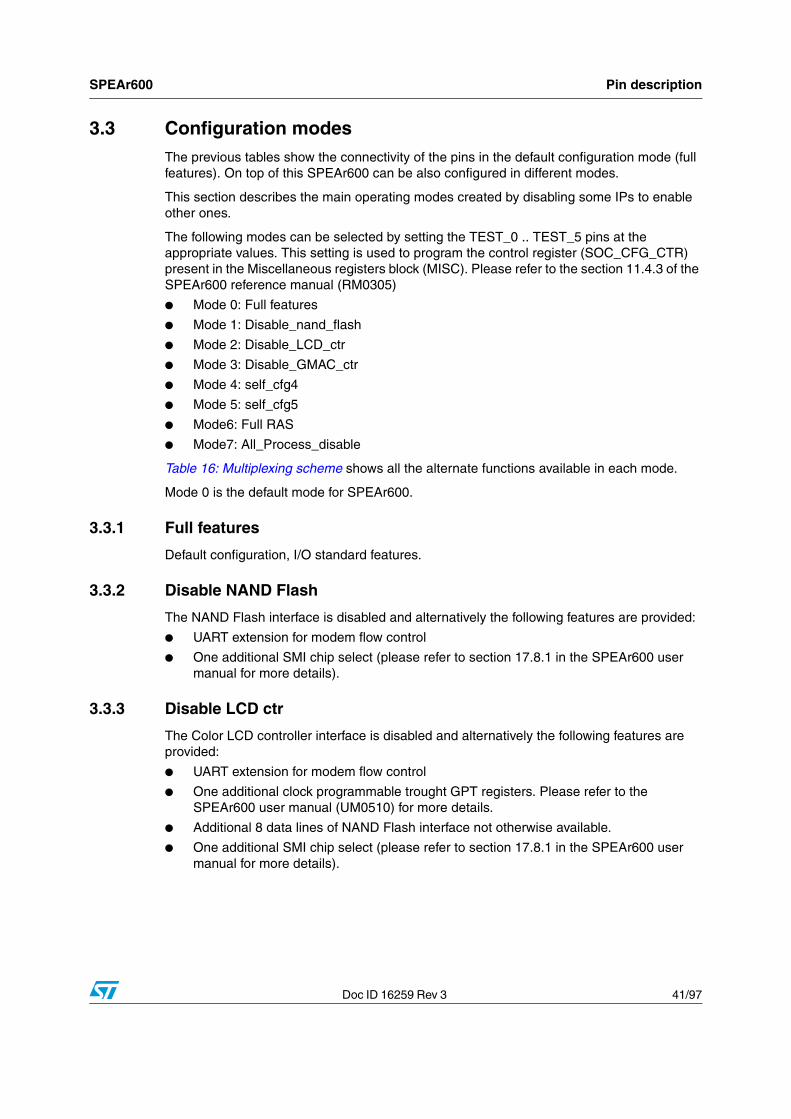
3.3 Configuration modesThe previous tables show the connectivity of the pins in the default configuration mode (full features). On top of this SPEAr600 can be also configured in different modes.
This section describes the main operating modes created by disabling some IPs to enable other ones.
The following modes can be selected by setting the TEST_0 .. TEST_5 pins at the appropriate values. This setting is used to program the control register (SOC_CFG_CTR) present in the Miscellaneous registers block (MISC). Please refer to the section 11.4.3 of the SPEAr600 reference manual (RM0305)
● Mode 0: Full features
● Mode 1: Disable_nand_flash
● Mode 2: Disable_LCD_ctr
● Mode 3: Disable_GMAC_ctr
● Mode 4: self_cfg4
● Mode 5: self_cfg5
● Mode6: Full RAS
● Mode7: All_Process_disable
Table 16: Multiplexing scheme shows all the alternate functions available in each mode.
Mode 0 is the default mode for SPEAr600.
3.3.1 Full features
Default configuration, I/O standard features.
3.3.2 Disable NAND Flash
The NAND Flash interface is disabled and alternatively the following features are provided:
● UART extension for modem flow control
● One additional SMI chip select (please refer to section 17.8.1 in the SPEAr600 user manual for more details).
3.3.3 Disable LCD ctr
The Color LCD controller interface is disabled and alternatively the following features are provided:
● UART extension for modem flow control
● One additional clock programmable trought GPT registers. Please refer to the SPEAr600 user manual (UM0510) for more details.
● Additional 8 data lines of NAND Flash interface not otherwise available.
● One additional SMI chip select (please refer to section 17.8.1 in the SPEAr600 user manual for more details).
Pin description SPEAr600
42/97 Doc ID 16259 Rev 3
3.3.4 Disable GMAC ctr
The GMAC interface is disabled and alternatively the following features are provided:
● Two UARTs : one with extension for modem flow control and one with simplified hardware flow control
● One additional SMI chip select (please refer to section 17.8.1 in the SPEAr600 user manual for more details).
● Four additional clocks programmable trough the GPT registers. Please refer to the SPEAr600 user manual (UM0510) for more details.
3.3.5 Self cfg_4
In this mode the AHB expansion interface is enabled on the PL_GPIO (83:0) pins. In this mode source clock and reset signals are provided from the external application logic.
3.3.6 Self cfg_5
In this mode the AHB expansion interface is enabled on the PL_GPIO (83:0) pins. In this mode source clock and reset signals are internally provided.
3.3.7 All processors disabled
This mode configures the SoC as an I/O slave target device controlled by an external master application (the internal processors can be disabled).
0xE110.0000 0xE11F.FFFF USB 2.0 device Configuration registers
0xE120.0000 0xE12F.FFFF USB 2.0 device Plug detect
0xE130.0000 0xE17F.FFFF - Reserved
0xE180.0000 0xE18F.FFFF USB2.0 EHCI 1
Memory map SPEAr600
54/97 Doc ID 16259 Rev 3
0xE190.0000 0xE19F.FFFF USB2.0 OHCI 1
0xE1A0.0000 0xE1FF.FFFF - Reserved
0xE200.0000 0xE20F.FFFF USB2.0 EHCI 2
0xE210.0000 0xE21F.FFFF USB2.0 OHCI 1
0xE220.0000 0xE27F.FFFF - Reserved
0xE280.0000 0xE28F.FFFFUSB AHB-Master Layer
arbiterConfiguration register
0xE290.0000 0xE7FF.FFFF - Reserved
0xE800.0000 0xEFFF.FFFF - Reserved
0xF000.0000 0xF00F.FFFF Timer
0xF010.0000 0xF01F.FFFF GPIO
0xF020.0000 0xF0FF.FFFF - Reserved
0xF100.0000 0xF10F.FFFF ITC Secondary
0xF110.0000 0xF11F.FFFF ITC Primary
0xF120.0000 0xF7FF.FFFF - Reserved
0xF800.0000 0xFBFF.FFFF Serial Flash Memory
0xFC00.0000 0xFC1F.FFFF Serial Flash Controller
0xFC20.0000 0xFC3F.FFFF LCD Controller
0xFC40.0000 0xFC5F.FFFF DMA Controller
0xFC60.0000 0xFC7F.FFFF SDRAM Controller
0xFC80.0000 0xFC87.FFFF Timer 1
0xFC88.0000 0xFC8F.FFFF Watchdog Timer
0xFC90.0000 0xFC97.FFFF Real time Clock
0xFC98.0000 0xFC9F.FFFF General Purpose I/O
0xFCA0.0000 0xFCA7.FFFF System Controller
0xFCA8.0000 0xFCAF.FFFF Miscellaneous Registers
0xFCB0.0000 0xFEFF.FFFF - Reserved
0xFF00.0000 0xFFFF.FFFF Internal ROM Boot
Table 18. Memory map (continued)
Start address End address Peripheral Description
SPEAr600 Electrical characteristics
Doc ID 16259 Rev 3 55/97
5 Electrical characteristics
5.1 Absolute maximum ratingsThis product contains devices to protect the inputs against damage due to high/low static voltages. However it is advisable to take normal precaution to avoid application of any voltage higher/lower than the specified maximum/minimum rated voltages.
The Absolute maximum rating is the maximum stress that can be applied to a device without causing permanent damage. However, extended exposure to minimum/maximum ratings may affect long-term device reliability.
5.2 Maximum power consumptionThe following table includes the maximum current and power consumption for each power domain.
Note: These values take into consideration the worst cases of process variation and voltage range and must be used to design the power supply section of the board.
Table 19. Absolute maximum ratings
Symbol Parameter Minimum value Maximum value Unit
VDD 1.0 Supply voltage at 1.0 - 0.3 1.2 V
VDD 3.3 Supply voltage at 3.3 - 0.3 3.9 V
VDD 2.5 Supply voltage at 2.5 - 0.3 3 V
VDD 1.8 Supply voltage at 1.8 - 0.3 2.16 V
TSTG Storage temperature -55 150 °C
TJ Junction temperature -40 125 °C
Table 20. Maximum current and power consumption
Symbol Description Max Unit
VDD 1.0 Supply voltage at 1.0 V 1000 mA
VDD 1.8 Supply voltage at 1.8 V(1)
1. Average current with Linux memory test [50% write and 50% read] plus DMA reading memory.
130 mA
VDD 2.5 Supply voltage at 2.5 V 22 mA
VDD 3.3 Supply voltage at 3.3 V(2)
2. With 30 logic channels connected to the device and simultaneously switching at 10 MHz.
60 mA
VDD RTC Supply voltage at 1.8 V 10 µA
PD Maximum power consumption 1500(3) mW
Electrical characteristics SPEAr600
56/97 Doc ID 16259 Rev 3
5.3 DC electrical characteristicsThe recommended operating conditions are listed in the following table:
5.4 Overshoot and undershootThis product can support the following values of overshoot and undershoot.
If the amplitude of the overshoot/undershoot increases (decreases), the ratio of overshoot/undershoot width to the pulse width decreases (increases). The formula relating the two is:
Amplitude of OS/US = 0.75*(1- ratio of OS (or US) duration with respect to pulse width)
Note: The value of overshoot/undershoot should not exceed the value of 0.5 V. However, the duration of the overshoot/undershoot can be increased by decreasing its amplitude.
3. The maximum current and power values listed above, obtained with typical supply voltages, are not guaranteed to be the highest obtainable. These values are dependent on many factors including the type of applications running, clock rates, use of internal functional capabilities, external interface usage, case temperature, and the power supply voltages. Your specific application can produce significantly different results.
1 V current and power are primarily dependent on the applications that are running and the use of internal chip functions (DMA, USB, Ethernet, and so on).
3.3 V current and power are primarily dependent on the capacitive loading, frequency, and utilization of the external buses.
Table 21. Recommended operating conditions
Symbol Parameter Min Typ Max Unit
VDD 1.0 Supply voltage at 1.0 0.95 1 1.10 V
VDD 3.3 Supply voltage at 3.3 3 3.3 3.6 V
VDD 2.5 Supply voltage at 2.5 2.25 2.5 2.75 V
VDD 1.8 Supply voltage at 1.8 1.70 1.8 1.9 V
VDDRTC Supply voltage at 1.8 1.62 1.8 1.98 V
TA Ambient temperature -40 85 °C
TJ Junction temperature -40 125 °C
Table 22. Overshoot and undershoot specifications
Parameter 3V3 I/Os 2V5 I/Os 1V8 I/Os
Amplitude 500 mV 500 mV 500 mV
Ratio of overshoot (or undershoot) duration with respect to pulse width
1/3 1/3 1/3
SPEAr600 Electrical characteristics
Doc ID 16259 Rev 3 57/97
5.5 3.3V I/O characteristicsThe 3.3 V I/Os are compliant with JEDEC standard JESD8b
5.6 DDR2 pin characteristics
Table 23. Low voltage TTL DC input specification (3 V< VDD <3.6 V)
Symbol Parameter Min Max Unit
VIL Low level input voltage 0.8 V
VIH High level input voltage 2 V
Vhyst Schmitt trigger hysteresis 300 800 mV
Table 24. Low voltage TTL DC output specification (3 V< VDD <3.6 V)
Symbol Parameter Test Condition Min Max Unit
VOL Low level output voltage IOL= X mA (1)
1. For the max current value (X mA) refer to Section 3: Pin description.
0.3 V
VOH High level output voltage IOH= -X mA (1) VDD - 0.3 V
Table 25. Pull-up and pull-down characteristics
Symbol Parameter Test Condition Min. Max Unit
RPU Equivalent pull-up resistance VI = 0 V 29 67 KΩ
RPDEquivalent pull-down
resistanceVI = VDDE3V3 29 103 KΩ
Table 26. DC characteristics
Symbol Parameter Test Condition Min. Max Unit
VIL Low level input voltageSSTL2 -0.3 VREF-0.15 V
SSTL18 -0.3 VREF-0.125 V
VIH High level input voltageSSTL2 VREF+0.15 VDDE2V5+0.3 V
SSTL18 VREF+0.125 VDDE1V8+0.3 V
Vhyst Input voltage hysteresis 200 mV
Table 27. Driver characteristics
Symbol Parameter Min Typ Max Unit
RO
Output impedance (strong value) 18.9 21 23.1 Ω
Output impendance (weak value) 32.9 35 37.1 Ω
Electrical characteristics SPEAr600
58/97 Doc ID 16259 Rev 3
5.7 Power up sequenceNo particular sequence is required. It is only required that the various power supplies reach the correct range in less than 10 msec.
5.8 Power on reset (MRESET) The MRESET must remain active for at least 10 ms after all the power supplies are in the correct range and should become active in no more than 10 µs when one of the power supplies goes out of the correct range.
Figure 3. Power on reset timing diagram
Table 28. On die termination
Symbol Parameter Min. Typ. Max Unit
RT1*Termination value of resistance for on die
termination75 Ω
RT2*Termination value of resistance for on die
termination150 Ω
Table 29. Reference voltage
Symbol Parameter Min. Typ. Max Unit
VREFIN Voltage applied to core/pad0.49 *
VDDE
0.500 *
VDDE
0.51 *
VDDEV
2.95 us
MRESET
resets_o
sclk
npor_o
hresetn
pll_lock
17 sclk clock cycles (at 30MHz)
All Vdd are stable
OSCI 30MHz
synch
synch60 clock cycles
synch
Pll lock time (note 2)
DOZE MODE NORMAL MODE
arm_fetching
10 ms
SPEAr600 Electrical characteristics
Doc ID 16259 Rev 3 59/97
Note: 1 The oscillator generates a stable clock 1.5 ms after the power supply becomes stable.
2 The Pll lock time is given by the following formula:
Lock time = 4 ms / (decimal equivalent of PLL charge pump bit setting + 1)
The PLL charge pump (CP) bits are in the PLL1/2_CTR register in the Miscellaneous register block. Please refer to the user manual for more details.
For example, if the application software sets CP = 01110 = 14 (decimal), then:
6.1 DDR2 timing characteristicsThe characterization timing is done considering an output load of 10 pF on all the DDR pads. The operating conditions are in worst case V = 0.90 V TA = 125 °C and in best case V=1.10 V TA = 40 °C.
6.1.1 DDR2 read cycle timings
Figure 4. DDR2 read cycle waveforms
Figure 5. DDR2 read cycle path
t4 t5 t5t4 t4
DQS
DQ
t1 t2Q
QSET
CLR
D
t3
DLLDQS
DQ
Table 31. DDR2 read cycle path timings without pad delay
t3MAX (t1 + t2)MIN t3MIN (t1 + t2)MAX
Rising best 133 ps 212 ps 125 ps 244 ps
Falling best 134 ps 205 ps 127 ps 239 ps
Rising worst 336 ps 611 ps 311 ps 646 ps
Falling worst 348 ps 550 ps 324 ps 590 ps
Table 32. DDR2 read cycle timings without pad delay
Period (T) Frequency t4MAX t5MAX
3 ns 333 MHz 814 ps 343 ps
3.75 ns 266 MHz 996 ps 532 ps
SPEAr600 Timing characteristics
Doc ID 16259 Rev 3 61/97
Table 32 shows the internal chip timing without the contribution of the pads.
These values are obtained considering the nominal setting of DLL at T/4 period, in fact, the DDR memory launches data (DQ) and data strobe (DQS) aligned. Internally the DQS is delayed by T/4 (DLL) to guarantee correct data capture.
The waveforms in Figure 4 refers to the pad or memory side: so the data move around the edges of DQS signals. In this case, we consider the maximum values for t4 and t5 to obtain the minimum data valid window. For correct data capture (at the controller side) the last arrival time of the data (last variation) must precede the first arrival of the data strobe:
Note: DQS (delay) is the combination of delays experienced by the DQS (data strobe) signal, DQ (delay) is the combination of delays experienced by the DQ (data) signal (both until the capture is performed by the controller).
DQS (delay) depends on t1 and t2 while DQ (delay) depends on t3.
6.1.2 DDR2 write cycle timings
Figure 6. DDR2 write cycle waveforms
5 ns 200 MHz 1.31 ns 842 ps
6 ns 166 MHz 1.56 ns 1.10 ns
7.5 ns 133 MHz 1.93 ns 1.47 ns
a. The value “one DLL element” stands for the DLL accuracy, so we put ± one DLL element in the formulas. One DLL element = 15 ps in best case and 85 ps in worst case.
Table 32. DDR2 read cycle timings without pad delay (continued)
Period (T) Frequency t4MAX t5MAX
t4 t5 t5t4
DQS
DQ
t4 t5
Timing characteristics SPEAr600
62/97 Doc ID 16259 Rev 3
Figure 7. DDR2 write cycle path
Table 34 shows the internal chip timing without the contribution of the pads.
These values are obtained considering the nominal setting of DLL at T period for DQS path and T*3/4 for DQ path, in fact the memory controller launches data (DQ) and data strobe (DQS) misaligned. Internally the clock is delayed by T to produce the DQS and the same clock is delayed by T*3/4 to clock the data DQ, in order to perform a correct write to the memory. The table values are measured in a particular pad configuration:
Drive strength = strong (zprog_out = L)
Slope : prog_a = L ; prog_b = H (corresponding to 266 MHz)
The waveforms in Figure 6 refer to the pad or memory side, so the DQS edges are centered on the data valid window. In this case, we consider the minimum values for t4 and t5 in order to obtain the minimum data valid window. For a correct data write (on the memory side) the last variation of the data must precede the first arrival of the data strobe. In other words, we can consider t4 as the tSETUP of the data that can be defined as the time range where the
Table 33. DDR2 write cycle path timings without pad delay
t3MAX (t1 + t2)MIN t3MIN (t1 + t2)MAX
Rising best 2.19 ns 2.08 ns 1.91 ns 2.13 ns
Falling best 2.21 ns 2.11 ns 1.95 ns 2.15 ns
Rising worst 5.55 ns 5.28 ns 5.2 ns 5.33 ns
Falling worst 5.54 ns 5.30 ns 5.3 ns 5.35 ns
Table 34. DDR2 write cycle timings without pad delay
Period (T) Frequency t4MIN t5MIN
3 ns 333 MHz 396 ps 492 ps
3.75 ns 266 MHz 585 ps 681 ps
5 ns 200 MHz 895 ps 991 ps
6 ns 166 MHz 1.15 ns 1.25 ns
7.5 ns 133 MHz 1.52 ns 1.62 ns
Q
QSET
CLR
D
Q
QSET
CLR
D
t1 t2
DLL2
t3
DQS
DQ
CLK
DLL1
SPEAr600 Timing characteristics
Doc ID 16259 Rev 3 63/97
data are stable before the arrival of the DQS. To have a positive quantity the delay obtained by the DQ (maximum delay or last variation) must be less than one obtained by the DQS (minimum delay).
So:
t4MIN = DQS (delay)MIN - DQ (delay)MAX = (t1MIN + T ± one DLL element(a) + t2MIN) - (T*3/4 ± one DLL element(a) + t3MAX) = t1MIN + T/4 + t2MIN ± one DLL element(a) - t3 MAX
t5 can be expressed in a similar way, and can be defined as the tHOLD of the data:
t5MIN = DQ (delay)MIN - DQS (delay)MAX = (T/2 + T*3/4 ± one DLL element(a) + t3MIN) - (t1MAX + T ± one DLL element(a) + t2MAX) =
Note: DQS (delay) is the combination of delays experienced by the DQS (data strobe) signal, DQ (delay) is the combination of delays experienced by the DQ (data) signal (both until the capture performed by the controller).
6.1.3 DDR2 command timings
Figure 8. DDR2 command waveforms
Figure 9. DDR2 command path
For the command and control timings, we have to consider that the commands are launched on the negative edge of the clock and are captured on the next positive edge of the clock.
a. The value “one DLL element” stands for the DLL accuracy, so we put ± one DLL element in the formulas. One DLL element = 15 ps in best case and 85 ps in worst case.
t4 t5
CLK
ADDRESS, STROBEs,and CONTROL LINES
Q
QSET
CLR
Dt2
t3
CLK
ADDRESS, STROBEs,and CONTROL LINES ADDRESS, STROBEs,
and CONTROL LINES
CLK
Timing characteristics SPEAr600
64/97 Doc ID 16259 Rev 3
Therefore, we have to add the value T to the clock path and the value T/2 to the command path.
The waveform shown in Figure 8 refers to the pad or memory side, so the CLK edges are centered on the command valid window. In this case, we consider the minimum values for t4 and t5 in order to obtain the minimum command valid window. We can consider t4 as the tSETUP of the commands that can be defined as the time range where the commands are stable before the arrival of the clock. To have a positive quantity the delay obtained by the commands (maximum delay or last variation) must be less than the one obtained by the clock (minimum delay).
Note: CLK(delay) is the combination of delays experienced by the CLK signal, CMD(delay) is the combination of delays experienced by the command/ctrl/address signal (both until the capture performed by the memory).
Table 35 shows the internal chip timing without the contribution of the pads.
Table 35. DDR2 command timings without pad delay
Period (T) Frequency t4MIN t5MIN
3 ns 333 MHz 977 ps 1.33 ns
3.75 ns 266 MHz 1.35 ns 1.71 ns
5 ns 200 MHz 1.98 ns 2.33 ns
6 ns 166 MHz 2.49 ns 2.84 ns
7.5 ns 133 MHz 3.23 ns 3.59 ns
SPEAr600 Timing characteristics
Doc ID 16259 Rev 3 65/97
6.2 EXPI timing characteristicsThe characterization timing is done for an output load of 10 pF on PL_CLKx and 5 pF on PL_GPIO_x .The operating conditions are in worst case V=0.90 V TA =125 °C and in best case V=1.10 V TA= 40 °C.
The timings are measured using TEST [5:0] = 101xxx: (Selg_cfg5 = EXPI with internal clock). Please refer to the user manual for the description of the SoC_cfg bits in the MISC registers.
Figure 10. AHB EXPI transfer waveforms
Table 36. EXPI - pad signal assignment
EXPI signal Direction PL_GPIOs signal assignment
HAdd(19:00) Bidir. PL_GPIO(19:00)
HAdd(21:20) Bidir. PL_GPIO(56:55)
HAdd(23-:22) Bidir. PL_GPIO(82:81)
HRWData(07:00) Bidir. PL_GPIO(27:20)
HRWData(15:08) Bidir. PL_GPIO(64:57)
HRWData(31:16) Bidir. PL_GPIO(80:65)
HSize(2-0) Bidir. PL_GPIO(30:28)
HWrite Bidir. PL_GPIO(31)
HBurst(2-0) Bidir. PL_GPIO(34:32)
HTrans(1-0) Bidir. PL_GPIO(36:35)
Timing characteristics SPEAr600
66/97 Doc ID 16259 Rev 3
Note: For more details please refer to the Expansion interface (EXPI) chapter of the user manual.
6.2.1 Pad delay disabled
Figure 11. Pad delay disabled block diagram
Note: The pad of the clock is disabled or enabled using the expi_clk_retim bit in the EXPI_CLK_CFG register. Refer to the MISC registers chapter of the user manual).
HLock Inp. PL_GPIO_37
HMastlock Out. PL_GPIO_38
HBreq Inp. PL_GPIO_39
HGrant Out. PL_GPIO_40
HResp(1-0) Bidir. PL_GPIO(42:41)
HReady_mst Out. PL_GPIO_43
HReady_out Inp. PL_GPIO_44
HReady_in Out. PL_GPIO_45
HSel Out. PL_GPIO_46
DMA_LREQ(1:0)/ HAdd(25:24) Inp. PL_GPIO(48:47)
DMA_REQ(1:0) / HAdd(27:26) Inp. PL_GPIO(50:49)
DMACCLR(1:0)/ HAdd(29:28) Out. PL_GPIO(52:51)
DMACTC(1:0) / HAdd(31:30) Out. PL_GPIO(54:53)
INT_IN_2 Inp. PL_GPIO_83
CLK Bidir. PL_CLK_1
Reset Bidir. PL_CLK_2
INT_IN_1 Inp. PL_CLK_3
INT_OUT Out. PL_CLK_4
Table 36. EXPI - pad signal assignment (continued)
Note: For tSETUP, tHOLD and tmax are taken the maximum value from worst case and best case, while the minimum value is taken for tmin.
6.2.2 Pad delay enabled
Figure 13. EXPI pad delay enabled block diagram
Note: The pad of the clock is disabled or enabled using the expi_clk_retim bit in the EXPI_CLK_CFG register. Refer to the MISC registers chapter of the user manual).
6.3 CLCD timing characteristicsThe characterization timing is done considering an output load of 10 pF on all the outputs.The operating conditions are in worst case V=0.90 V T=125 °C and in best case V=1.10 V T= 40 °C.
The CLCD has a wide variety of configurations and setting and the parameters change accordingly. Two main scenarios will be considered, one with direct clock to output (166 MHz), setting BCD bit to '1', and the second one with the clock passing through a clock divider (83 MHz), setting BCD bit to '0'. Please refer to the Table 477 for more information on the significance of bit BCD).
6.3.1 CLCD timing characteristics direct clock
Figure 15. CLCD waveform with CLCP direct
Figure 16. CLCD block diagram with CLCP direct
Table 43. CLCD timings with CLCP direct
Parameter Value Frequency
Tclock direct max (Tclock) 6 ns 166 MHz
Tclock direct max rise (Tr) 0.81 ns
Tclock direct max (Tf) 0.87 ns
Tmin -0.04 ns
Tmax 3.62 ns
Tstable 2.34 ns
Tmin
TmaxCLCP
CLD[23:0], CLAC, CLLE, CLLP, CLFP, CLPOWER
Tclock
TrTfTstable
Q
QSET
CLR
Dt2
t3CLCP
CLD[23:0], CLAC, CLLE, CLLP, CLFP, CLPOWERCLCDCLK
t1
Timing characteristics SPEAr600
72/97 Doc ID 16259 Rev 3
Note: 1 Tstable = Tclock direct max - (Tmax + Tmin)
2 For Tmax the maximum value is taken from the worst case and best case, while for Tmin the minimum value is taken from the worst case and best case.
3 CLCP should be delayed by {Tmax + [Tclock direct max - (Tmax + Tmin)]/2} = 4.7915 ns
6.3.2 CLCD timing characteristics divided clock
Figure 17. CLCD waveform with CLCP divided
Figure 18. CLCD block diagram with CLCP divided
Table 44. CLCD timings with CLCP divided
Parameter Value Frequency
Tclock divided max 12 ns 83.3 MHz
Tclock divided max rise (Tr) 0.81 ns
Tclock divided max (Tf) 0.87 ns
Tmin -0.49 ns
Tmax 2.38 ns
Tstable 9.13 ns
Tmin
Tmax
CLCP
CLD[23:0], CLAC, CLLE, CLLP, CLFP, CLPOWER
Tclock
TrTfTstable
Q
QSET
CLR
Dt2
CLCP
CLD[23:0], CLAC, CLLE,CLLP, CLFP, CLPOWERCLCDCLK
t1
Q
QSET
CLR
D t3
SPEAr600 Timing characteristics
Doc ID 16259 Rev 3 73/97
Note: 1 Tstable = Tclock direct max - (Tmax + Tmin)
2 For Tmax the maximum value is taken from the worst case and for Tmin the minimum value is taken from the best case.
3 CLCP should be delayed by {Tmax + [Tclock direct max - (Tmax + Tmin)]/2} = 6.945 ns
6.4 I2C timing characteristicsThe characterization timing is given for an output load of 10 pF on SCL and SDA.
The operating conditions are V=0.90 V, T=125 °C in worst case and V=1.10 V, TA= 40 °C in best case.
Figure 19. I2C output pads
Figure 20. I2C input pads
The flip-flops used to capture the incoming signals are re-synchronized with the AHB clock: so no input delay calculation is required.
Q
QSET
CLR
D
Q
QSET
CLR
D
HCLK
SCL
SDA
Q
QSET
CLR
D
Q
QSET
CLR
D
HCLK
SDA
SCL
Q
QSET
CLR
D
Q
QSET
CLR
D
Timing characteristics SPEAr600
74/97 Doc ID 16259 Rev 3
Figure 21. Output signal waveforms for I2C signals
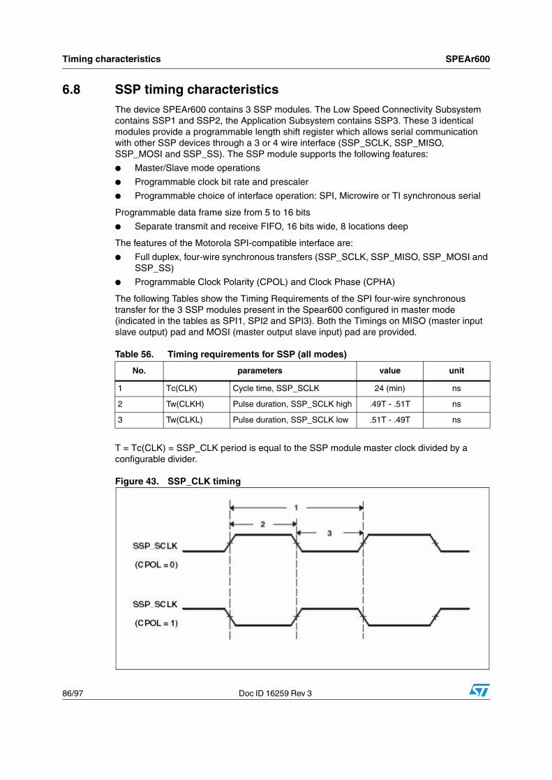
The timings of high and low level of SCL (TSCLHigh and TSCLLow) are programmable.
Table 45. Timing characteristics for I2C in high-speed mode
Parameter Min
TSU-STA 163.31 ns
THD-STA 487.73 ns
TSU-DAT 313.38 ns
THD-DAT 7.04 ns
TSU-STO 642.98 ns
THD-STO 4.74 µs
Table 46. Timing characteristics for I2C in fast-speed mode
Parameter Min
TSU-STA 643.27 ns
THD-STA 601.73 ns
TSU-DAT 1.19 µs
THD-DAT 7.04 ns
TSU-STO 642.98 ns
THD-STO 4.74 µs
Table 47. Timing characteristics for I2C in standard-speed mode
Parameter Min
TSU-STA 4.73 µs
THD-STA 3.99 µs
TSU-DAT 4.67 µs
THD-DAT 7.04 ns
TSU-STO 4.03 µs
THD-STO 4.74 µs
SCL
TSU-STA
SDA
THD- STA THD-DAT TSU-STOTHD- STO
TSCLHigh TSCLLow
TSU-DAT
SPEAr600 Timing characteristics
Doc ID 16259 Rev 3 75/97
Note: The timings shown in Figure 21 depend on the programmed values of TSCLHigh and TSCLLow: so, the values present in Table 45 to Table 47 have been calculated using the minimum programmable values of:
IC_HS_SCL_HCNT=19 and IC_HS_SCL_LCNT=53 registers (for High-Speed mode)
IC_FS_SCL_HCNT=99 and IC_FS_SCL_LCNT=215 registers (for Fast-Speed mode)
IC_SS_SCL_HCNT=664 and IC_SS_SCL_LCNT=780 registers (for Standard-Speed mode).
These minimum values depend on the AHB clock frequency, which is 166 MHz.
Note: A device may internally require a hold time of at least 300 ns for the SDA signal (referred to the VIHmin of the SCL signal) to bridge the undefined region of the falling edge of SCL (Please refer to the I2C Bus Specification v3-0 Jun 2007). However, the SDA data hold time in the I2C controller of SPEAr600 is one-clock cycle based (7 ns with the HCLK clock at 166 MHz). This time may be insufficient for some slave devices. A few slave devices may not receive the valid address due to the lack of SDA hold time and will not acknowledge even if the address is valid. If the SDA data hold time is insufficient, an error may occur.
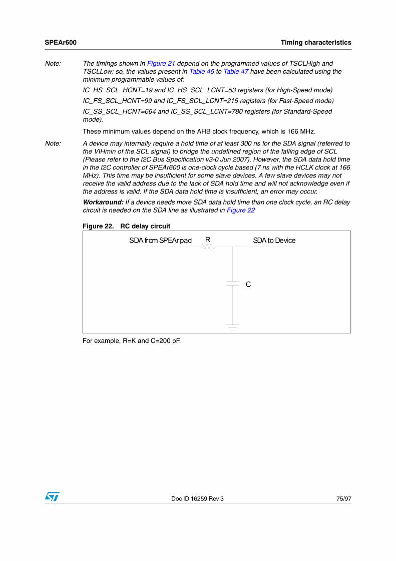
Workaround: If a device needs more SDA data hold time than one clock cycle, an RC delay circuit is needed on the SDA line as illustrated in Figure 22
Figure 22. RC delay circuit
For example, R=K and C=200 pF.
SDA from SPEAr pad SDA to DeviceR
C
Timing characteristics SPEAr600
76/97 Doc ID 16259 Rev 3
6.5 FSMC timing characteristicsThe characterization timing is done using primetime considering an output load of 3 pF on the data, 15 pF on NF_CE, NF_RE and NF_WE and 10 pF on NF_ALE and NF_CLE.
The operating conditions are V=0.90 V, T=125 °C in worst case and V=1.10 V, T= 40 °C in best case.
6.5.1 8-bit NAND Flash configuration
Figure 23. Output pads for 8-bit NAND Flash configuration
Figure 24. Input pads for 8-bit NAND Flash configuration
Figure 25. Output command signal waveforms for 8-bit NAND Flash configuration
Q
QSET
CLR
D
Q
QSET
CLR
D
HCLK
NFALE
NFCLE
NFIO_0..7
NFCENFWENFRE
NFRWPRT... ...
...
Q
QSET
CLR
D
Q
QSET
CLR
D
HCLK
NFIO_0..7
NFRB
NFCLE
NFCE
NFWE
NFIO Command
TCLE
TWE
TIO
SPEAr600 Timing characteristics
Doc ID 16259 Rev 3 77/97
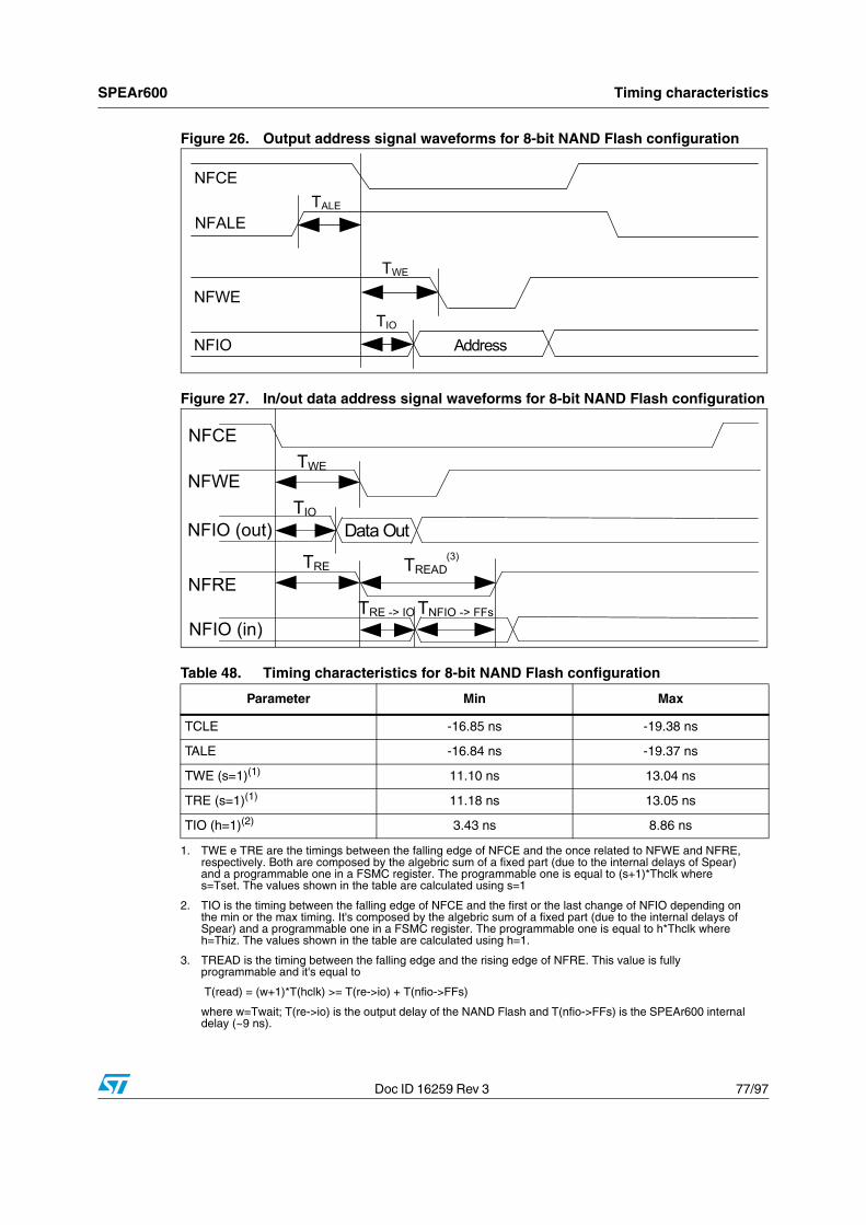
Figure 26. Output address signal waveforms for 8-bit NAND Flash configuration
Figure 27. In/out data address signal waveforms for 8-bit NAND Flash configuration
Table 48. Timing characteristics for 8-bit NAND Flash configuration
Parameter Min Max
TCLE -16.85 ns -19.38 ns
TALE -16.84 ns -19.37 ns
TWE (s=1)(1)
1. TWE e TRE are the timings between the falling edge of NFCE and the once related to NFWE and NFRE, respectively. Both are composed by the algebric sum of a fixed part (due to the internal delays of Spear) and a programmable one in a FSMC register. The programmable one is equal to (s+1)*Thclk where s=Tset. The values shown in the table are calculated using s=1
11.10 ns 13.04 ns
TRE (s=1)(1) 11.18 ns 13.05 ns
TIO (h=1)(2)
2. TIO is the timing between the falling edge of NFCE and the first or the last change of NFIO depending on the min or the max timing. It's composed by the algebric sum of a fixed part (due to the internal delays of Spear) and a programmable one in a FSMC register. The programmable one is equal to h*Thclk where h=Thiz. The values shown in the table are calculated using h=1.
3. TREAD is the timing between the falling edge and the rising edge of NFRE. This value is fully programmable and it's equal to
where w=Twait; T(re->io) is the output delay of the NAND Flash and T(nfio->FFs) is the SPEAr600 internal delay (~9 ns).
3.43 ns 8.86 ns
NFALE
NFCE
NFWE
NFIO Address
TALE
TWE
TIO
NFCE
NFWE
NFIO (out) Data OutTIO
NFIO (in)
NFRETRE -> IO
TWE
TRE TREAD
TNFIO -> FFs
(3)
Timing characteristics SPEAr600
78/97 Doc ID 16259 Rev 3
Note: Values in Table 48 are referred to the common internal source clock which has a period of THCLK = 6 ns.
6.5.2 16-bit NAND Flash configuration
Figure 28. Output pads for 16-bit NAND Flash configuration
Figure 29. Input pads for 16-bit NAND Flash configuration
Figure 30. Output command signal waveforms 16-bit NAND Flash configuration
Q
QSET
CLR
D
Q
QSET
CLR
D
HCLK
NFALE
NFCLE
NFIO_0..7
NFCENFWENFRE
NFRWPRT
... ... ... CLPOWERCLLPCLLECLFPCLCPCLAC
CLD_23..22
(NFIO_8..15)
Q
QSET
CLR
D
Q
QSET
CLR
D
HCLKNFIO_0..7NFRB
... ...
CLPOWERCLLPCLLECLFPCLCPCLACCLD_23..22
(NFIO_8..15)
NFCLE
NFCE
NFWE
NFIO Command
TCLE
TWE
TIO
SPEAr600 Timing characteristics
Doc ID 16259 Rev 3 79/97
Figure 31. Output address signal waveforms 16-bit NAND Flash configuration
Figure 32. In/out data signal waveforms for 16-bit NAND Flash configuration
Table 49. Timing characteristics for 16-bit NAND Flash configuration
Parameter Min Max
TCLE -16.85 ns -19.38 ns
TALE -16.84 ns -19.37 ns
TWE (s=1)(1)
1. TWE e TRE are the timings between the falling edge of NFCE and the once related to NFWE and NFRE, respectively. Both are composed by the algebric sum of a fixed part (due to the internal delays of Spear) and a programmable one in a FSMC register. The programmable one is equal to (s+1)*Thclk where s=Tset. The values shown in the table are calculated using s=1
11.10 ns 13.04 ns
TRE (s=1)(1) 11.18 ns 13.05 ns
TIO (h=1)(2)
2. TIO is the timing between the falling edge of NFCE and the first or the last change of NFIO depending on the min or the max timing. It's composed by the algebric sum of a fixed part (due to the internal delays of Spear) and a programmable one in a FSMC register. The programmable one is equal to h*Thclk where h=Thiz. The values shown in the table are calculated using h=1.
3. TREAD is the timing between the falling edge and the rising edge of NFRE. This value is fully programmable and it's equal to
where w=Twait; T(re->io) is the output delay of the NAND Flash and T(nfio->FFs) is the SPEAr600 internal delay (~9 ns).
3.27 ns 11.35 ns
NFALE
NFCE
NFWE
NFIO Address
TALE
TWE
TIO
NFCE
NFWE
NFIO (out) Data OutTIO
NFIO (in)
NFRETRE -> IO
TWE
TRE TREAD
TNFIO -> FFs
(3)
Timing characteristics SPEAr600
80/97 Doc ID 16259 Rev 3
Note: Values in Table 49 are referred to the common internal source clock which has a period of THCLK = 6 ns.
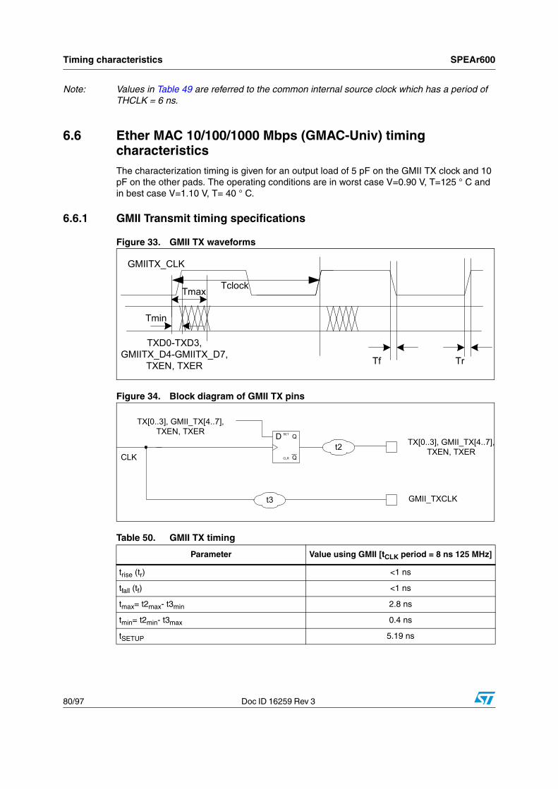
6.6 Ether MAC 10/100/1000 Mbps (GMAC-Univ) timing characteristicsThe characterization timing is given for an output load of 5 pF on the GMII TX clock and 10 pF on the other pads. The operating conditions are in worst case V=0.90 V, T=125 ° C and in best case V=1.10 V, T= 40 ° C.
6.6.1 GMII Transmit timing specifications
Figure 33. GMII TX waveforms
Figure 34. Block diagram of GMII TX pins
Table 50. GMII TX timing
Parameter Value using GMII [tCLK period = 8 ns 125 MHz]
trise (tr) <1 ns
tfall (tf) <1 ns
tmax= t2max- t3min 2.8 ns
tmin= t2min- t3max 0.4 ns
tSETUP 5.19 ns
Tmin
Tmax
GMIITX_CLK
TXD0-TXD3, GMIITX_D4-GMIITX_D7,
TXEN, TXER
Tclock
TrTf
Q
QSET
CLR
Dt2
t3 GMII_TXCLK
TX[0..3], GMII_TX[4..7],TXEN, TXERCLK
TX[0..3], GMII_TX[4..7], TXEN, TXER
SPEAr600 Timing characteristics
Doc ID 16259 Rev 3 81/97
Note: To calculate the tSETUP value for the PHY you have to consider the next tCLK rising edge, so you have to apply the following formula: tSETUP = tCLK - tmax
6.6.2 MII transmit timing specifications
Figure 35. MII TX waveforms
Figure 36. Block diagram of MII TX pins
Note: To calculate the tSETUP value for the PHY you have to consider the next tCLK rising edge, so you have to apply the following formula: tSETUP = tCLK - tmax
Table 51. MII TX timings
ParameterValue using MII 100 Mb [tCLK
period = 40 ns 25 MHz]Value using MII 10 Mb [tCLK
period = 400 ns 2.5 MHz]
tmax= t2max- t3min 6.8 ns 6.8 ns
tmin= t2min- t3max 2.9 ns 2.9 ns
tSETUP 33.2 ns 393.2 ns
TXD0-TXD3
Tmin
Tmax
TX_CLK
Tclock
TrTf
Q
QSET
CLR
Dt2
t3 TX_CLK
TXD[0..3]
TX[0..3]
Timing characteristics SPEAr600
82/97 Doc ID 16259 Rev 3
6.6.3 GMII-MII Receive timing specifications
Figure 37. GMII-MII RX waveforms
Figure 38. Block diagram of GMII-MII RX pins
Note: The input stage is the same for all the interfaces (GMII and MII10/100) so tSETUP and tHOLD values are equal in all the cases.
The receive path is optimized for the GMII interface: this also ensures correct capture of data for the MII10/100 interface.
Table 52. GMII-MII RX timings
Parameter
Value using GMII [tCLK
period = 8 ns
125 MHz]
Value using MII 100Mb
[tCLK period = 40 ns
25 MHz]
Value using MII 10
Mb [tCLK period = 400
ns 2.5 MHz]
tSETUPmax (tS)= t2max -t1min
2.26 ns 2.26 ns 2.26 ns
t HOLDmin (tH)= t2min -
t1max-0.11 ns -0.11 ns -0.11 ns
RXD0-RXD3, GMIIRX_D4-GMIIRX_D7,
RX_ER, RX_DV
RX_CLK
Ts
Th
Tclock
TrTf
t1Q
QSET
CLR
D
t2
RX[0..3], GMII_RX[4..7], RX_ER, RX_DV
RX_CLK
SPEAr600 Timing characteristics
Doc ID 16259 Rev 3 83/97
6.6.4 MDIO timing specifications
Figure 39. MDC waveforms
Figure 40. Paths from MDC/MDIO pads
Note: When MDIO is used as output the data are launched on the falling edge of the clock as shown in Figure 39.
Table 53. MDC/MDIO timing
Parameter Value Frequency
tCLK period 614.4 ns 1.63 MHz
tCLK fall (tf) 1.18 ns
tCLK rise (tr) 1.14 ns
Output
tmax = ~tCLK /2 307 ns
tmin = ~tCLK /2 307 ns
Input
tSETUPmax = t1max - t3min 6.88 ns
tHOLDmin = t1min - t3max -1.54 ns
Input Thold
MDC
MDIO
Tclock
TrTf
Output
Tsetup
TminTmax
Q
QSET
CLR
D
t2
t3
CLKMDIO
t1
Q
Q SET
CLR
D
MDC
INPUT
OUTPUT
Timing characteristics SPEAr600
84/97 Doc ID 16259 Rev 3
6.7 SMI timing characteristicsThe characterization timing is given for an output load of 5 pF on the clock and 10 pF on the other pads. The operating conditions are in worst case V=0.90 V, TA=125° C and in best case V=1.10 V, TA= 40° C.
6.7.1 SMI timing specifications
Figure 41. SMI waveforms
Figure 42. Block diagram of the SMI pins
Table 54. SMI timings in default configuration
Signal Parameter Value Description
SMI_CLK
tCLK 50 ns SMI period (normal mode).
tCLK 20 ns SMI period (fast read mode).
tr 0.8 nsTransition times.
tf 0.84 ns
SMI_DATAINtSETUP 4.5 ns Max setup time and min hold time of
data in, referred to SMI_CLK rising edge. tHOLD -0.08 ns
Thold
SMI_CLK
SMI_DATAIN
Tclock
TrT fTsetup
Tmin Tmax
SM I_DATAOUT
Tfmin Tfmax
SM I_CS_0SM I_CS_1SM I_CS_3 Trmin Trmax
Q
QS ET
C LR
D
Q
Q S ET
C LR
D
Q
QS ET
C LR
D
SMI_CLK
SMI_CLK
SMI_DATAIN
SMI_DATAOUTSMI_CS_n (n= 0,1,3)
SMI_DATAOUTSMI_CS_n (n= 0,1,3)
HCLK
SPEAr600 Timing characteristics
Doc ID 16259 Rev 3 85/97
SMI_DATAOUTtmax 0.65 ns Max and min delay time of data out,
referred to SMI_CLK falling edge.tmin -0.41 ns
SMI_CS_0
trmax 0.59 ns Max and min delay time of chip select 0 rising edge, referred to SMI_CLK falling edge.trmin -0.52 ns
tfmax 0.46 ns Max and min delay time of chip select 0 falling edge, referred to SMI_CLK falling edge.tfmin -052 ns
SMI_CS_1
trmax 0.67 ns Max and min delay time of chip select 0 rising edge, referred to SMI_CLK falling edge.trmin -0.27 ns
tfmax 0.54 ns Max and min delay time of chip select 1 falling edge, referred to SMI_CLK falling edge.tfmin -0.3 ns
Table 55. SMI Timings of SMI_CS_3 in non-default configurations
Signal Parameter Value Description
NF_WP (SMI_CS_3 in Disable_nand_flash)
trmax 2.64 ns Max and min delay time of chip select 3 rising edge, referred to SMI_CLK falling edge.trmin 1.32 ns
tfmax 2.47 ns Max and min delay time of chip select 3 falling edge, referred to SMI_CLK falling edge.tfmin -0.31 ns
CLD_14 (SMI_CS_3 in Disable_LCD_ctr)
trmax 0.71ns Max and min delay time of chip select 3 rising edge, referred to SMI_CLK falling edge.trmin -0.08 ns
tfmax 0.52 ns Max and min delay time of chip select 3 falling edge, referred to SMI_CLK falling edge.tfmin 0.36 ns
RX_ER (SMI_CS_3 in Disable_GMAC_ctr)
trmax 3.99 ns Max and min delay time of chip select 3 rising edge, referred to SMI_CLK falling edge.trmin 0.6 ns
tfmax 3.91 nsMax and min delay time of chip select 3 falling edge, referred to SMI_CLK falling edge.
tfmin 1.56 ns
trmin 1.32 ns
tfmax 2.47 ns Max and min delay time of chip select 3 falling edge, referred to SMI_CLK falling edge.tfmin 1.56 ns
Table 54. SMI timings in default configuration (continued)
Signal Parameter Value Description
Timing characteristics SPEAr600
86/97 Doc ID 16259 Rev 3
6.8 SSP timing characteristicsThe device SPEAr600 contains 3 SSP modules. The Low Speed Connectivity Subsystem contains SSP1 and SSP2, the Application Subsystem contains SSP3. These 3 identical modules provide a programmable length shift register which allows serial communication with other SSP devices through a 3 or 4 wire interface (SSP_SCLK, SSP_MISO, SSP_MOSI and SSP_SS). The SSP module supports the following features:
● Master/Slave mode operations
● Programmable clock bit rate and prescaler
● Programmable choice of interface operation: SPI, Microwire or TI synchronous serial
Programmable data frame size from 5 to 16 bits
● Separate transmit and receive FIFO, 16 bits wide, 8 locations deep
The features of the Motorola SPI-compatible interface are:
● Full duplex, four-wire synchronous transfers (SSP_SCLK, SSP_MISO, SSP_MOSI and SSP_SS)
● Programmable Clock Polarity (CPOL) and Clock Phase (CPHA)
The following Tables show the Timing Requirements of the SPI four-wire synchronous transfer for the 3 SSP modules present in the Spear600 configured in master mode (indicated in the tables as SPI1, SPI2 and SPI3). Both the Timings on MISO (master input slave output) pad and MOSI (master output slave input) pad are provided.
T = Tc(CLK) = SSP_CLK period is equal to the SSP module master clock divided by a configurable divider.
Figure 43. SSP_CLK timing
Table 56. Timing requirements for SSP (all modes)
No. parameters value unit
1 Tc(CLK) Cycle time, SSP_SCLK 24 (min) ns
2 Tw(CLKH) Pulse duration, SSP_SCLK high .49T - .51T ns
The Motorola SPI interface is a four-wire interface where SSP_SS signal behaves as a slave select.
The main feature of the Motorola SPI format is that the inactive state and phase of the output clock signal are programmable through the CPOL (clock polarity) and CPHA (clock phase) parameters inside an IP control register.
● CPOL, clock polarity:
When CPOL clock polarity control parameter is low, it produces a steady state low value on the output clock pin. If this parameter is high, a steady state high value is placed on the output clock pin when data is not being transferred.
● CPHA, clock phase:
The CPHA clock phase control parameter selects the clock edge that captures data and allows it to change state. When CPHA is low, data is captured on the first clock edge transition after slave selection and is changed on the second clock edge transition. If the CPHA clock phase control parameter is high, data is captured on the second clock edge transition after the slave selection and is changed on the first clock edge transition.
6.8.1 SPI master mode timings (CPHA = 0)
Table 57. Timing requirements for SPI mode on MISO pad [CPHA = 0]
No parameters CPOL SPI1 SPI2 SPI3 unit
13Setup time, MISO (input) valid before SSP_SCLK (output) rising edge
0 9.563 10.759 10.357 ns
14Setup time, MISO (input) valid before SSP_SCLK (output) falling edge
1 9.632 10.804 10.427 ns
15Hold time, MISO (input) valid after SSP_SCLK (output) rising edge
0 -8.849 -10.112 -9.753 ns
16Hold time, MISO (input) valid after SSP_SCLK (output) falling edge
1 -8.956 -10.149 -9.785 ns
Table 58. Timing requirements for SPI mode on MOSI pad [CPHA = 0]
No parameters CPOL SPI1 SPI2 SPI3 unit
17Delay time, SSP_SCLK (output) falling edge to MOSI (output) transition
0 -0.675 -1.141 -1.638 ns
18Delay time, SSP_SCLK (output) rising edge to MOSI (output) transition
6Hold time, MISO (input) valid after SSP_SCLK (output) falling edge
0 -8.956 -10.149 -9.785 ns
7Hold time, MISO (input) valid after SSP_SCLK (output) rising edge
1 -8.849 -10.112 -9.753 ns
Table 60. Timing requirements for SPI mode on MOSI pad [CPHA = 1]
No parameters CPOL SPI1 SPI2 SPI3 unit
8Delay time, SSP_SCLK (output) rising edge to MOSI (output) transition
0 -0.607 -1.097 -1.568 ns
9Delay time, SSP_SCLK (output) falling edge to MOSI (output) transition
1 -0.675 -1.141 -1.638 ns
10
Delay time, SSP_SS (output) falling edge to first SSP_SCLK (output) rising or falling edge
T/2 ns
11
Delay time, SSP_SCLK (output) rising or falling edge to SSP_SS (output) rising edge
T/2 ns
Table 59. Timing requirements for SPI mode on MISO pad [CPHA = 1] (continued)
No parameters CPOL SPI1 SPI2 SPI3 unit
Package information SPEAr600
90/97 Doc ID 16259 Rev 3
7 Package information
In order to meet environmental requirements, ST offers these devices in different grades of ECOPACK® packages, depending on their level of environmental compliance. ECOPACK® specifications, grade definitions and product status are available at: www.st.com. ECOPACK® is an ST trademark.
Added a line of explanation in the introduction of Section 3: Pin description.
Added new Section 3.3: Configuration modes.Added new Section 2.25: External Port Controller (EXPI I/F).
Table 63. Document revision history (continued)
Date Revision Changes
Revision history SPEAr600
96/97 Doc ID 16259 Rev 3
09-May-2012 3
Modified FSMC feature on page 1
Figure 2: Typical system architecture using SPEAr600:
– Deleted SRAM and ROM blocks which were connected to the FSMC block
– Substituted SSP with 3xSSP– Added the RAS block.
Section 1.1: Main features on page 9:
– Deleted the word “/parallel” from bullet seven (about FSMC)– Replaced SPI with SSP in bullet sixteen.
– Modified number of GPIOs to 10
– Added information about RAS (Reconfigurable Array Subsystem)Chapter 2: Architecture overview: reviewed the first introduction part.
Section 2.4: Flexible static memory controller:
– Updated the introduction.
– Main features: changed the sentence “Provides independent chip select for each memory bank" by "Provides only one chip select for the first memory bank"
Table 3: Power supply pins: swapped ball R1 from the “Digital ground group” to the “Analog ground group”.
Section 2.15: UARTs: corrected the value of the baud rate to 3 Mbps
Table 48: Timing characteristics for 8-bit NAND Flash configuration and Table 49: Timing characteristics for 16-bit NAND Flash configuration: added three footnotes.
Table 3: Power supply pins: swapped ball R1 from the “Digital ground group” to the “Analog ground group”.
Section 2.15: UARTs: corrected the value of the baud rate in 3 Mbps
Table 48: Timing characteristics for 8-bit NAND Flash configuration and Table 49: Timing characteristics for 16-bit NAND Flash configuration: added three footnotes.
Created the new Section 2.24: Reconfigurable array subsystem connectivity (RAS).
Section 3.3: Configuration modes and Section Table 16.: Multiplexing scheme: removed additional PL_GPIOs, PL_CLK signals and renamed GPIOs to EXPI IOs Section 6.6.3: GMII-MII Receive timing specifications: added Table 52: GMII-MII RX timings.Changed parameter TO to TA and added TJ in Table 21: Recommended operating conditionsUpdated Table 62: SPEAr600 PBGA420 thermal resistance characteristics.
Table 63. Document revision history (continued)
Date Revision Changes
SPEAr600
Doc ID 16259 Rev 3 97/97
Please Read Carefully:
Information in this document is provided solely in connection with ST products. STMicroelectronics NV and its subsidiaries (“ST”) reserve theright to make changes, corrections, modifications or improvements, to this document, and the products and services described herein at anytime, without notice.
All ST products are sold pursuant to ST’s terms and conditions of sale.
Purchasers are solely responsible for the choice, selection and use of the ST products and services described herein, and ST assumes noliability whatsoever relating to the choice, selection or use of the ST products and services described herein.
No license, express or implied, by estoppel or otherwise, to any intellectual property rights is granted under this document. If any part of thisdocument refers to any third party products or services it shall not be deemed a license grant by ST for the use of such third party productsor services, or any intellectual property contained therein or considered as a warranty covering the use in any manner whatsoever of suchthird party products or services or any intellectual property contained therein.
UNLESS OTHERWISE SET FORTH IN ST’S TERMS AND CONDITIONS OF SALE ST DISCLAIMS ANY EXPRESS OR IMPLIEDWARRANTY WITH RESPECT TO THE USE AND/OR SALE OF ST PRODUCTS INCLUDING WITHOUT LIMITATION IMPLIEDWARRANTIES OF MERCHANTABILITY, FITNESS FOR A PARTICULAR PURPOSE (AND THEIR EQUIVALENTS UNDER THE LAWSOF ANY JURISDICTION), OR INFRINGEMENT OF ANY PATENT, COPYRIGHT OR OTHER INTELLECTUAL PROPERTY RIGHT.
UNLESS EXPRESSLY APPROVED IN WRITING BY TWO AUTHORIZED ST REPRESENTATIVES, ST PRODUCTS ARE NOTRECOMMENDED, AUTHORIZED OR WARRANTED FOR USE IN MILITARY, AIR CRAFT, SPACE, LIFE SAVING, OR LIFE SUSTAININGAPPLICATIONS, NOR IN PRODUCTS OR SYSTEMS WHERE FAILURE OR MALFUNCTION MAY RESULT IN PERSONAL INJURY,DEATH, OR SEVERE PROPERTY OR ENVIRONMENTAL DAMAGE. ST PRODUCTS WHICH ARE NOT SPECIFIED AS "AUTOMOTIVEGRADE" MAY ONLY BE USED IN AUTOMOTIVE APPLICATIONS AT USER’S OWN RISK.
Resale of ST products with provisions different from the statements and/or technical features set forth in this document shall immediately voidany warranty granted by ST for the ST product or service described herein and shall not create or extend in any manner whatsoever, anyliability of ST.
ST and the ST logo are trademarks or registered trademarks of ST in various countries.
Information in this document supersedes and replaces all information previously supplied.
The ST logo is a registered trademark of STMicroelectronics. All other names are the property of their respective owners.
Australia - Belgium - Brazil - Canada - China - Czech Republic - Finland - France - Germany - Hong Kong - India - Israel - Italy - Japan - Malaysia - Malta - Morocco - Philippines - Singapore - Spain - Sweden - Switzerland - United Kingdom - United States of America