19
By Fateen Mubarak EMBEDDED SYSTEMS DESIGN (EE 4314) 1 Embedded Systems Design (CE-14376) Fateen Mubarak Lecture # 17 21 st Nov 2013
| Date post: | 03-Jun-2018 |
| Category: |
Documents |
| Upload: | saad-mehtar |
| View: | 220 times |
| Download: | 0 times |

8/12/2019 embedded system session 8
http://slidepdf.com/reader/full/embedded-system-session-8 1/19
By Fateen Mubarak EMBEDDED SYSTEMS DESIGN (EE 4314) 1
Embedded Systems Design(CE-14376)
Fateen MubarakLecture # 17
21st Nov 2013

8/12/2019 embedded system session 8
http://slidepdf.com/reader/full/embedded-system-session-8 2/19
By Fateen Mubarak EMBEDDED SYSTEMS DESIGN (EE 4314) 2
SPI
• Serial Peripheral Interface (SPI) is ahardware/firmware communications
protocol developed by Motorola and later
adopted by others in the industry.• A serial peripheral interface (SPI) has a
simple 4-wire synchronous interface
protocol that enables controllers andperipheral devices to intercommunicate.
• It’s a Serial Communication Protocol.

8/12/2019 embedded system session 8
http://slidepdf.com/reader/full/embedded-system-session-8 3/19
By Fateen Mubarak EMBEDDED SYSTEMS DESIGN (EE 4314) 3
Serial Peripheral Interface
• Operates in full duplex mode
• It can support 1 Mbps or 10Mbps of speed.
• Both single-master and multi-master
protocols are possible in SPI.
– But the multi-master bus is rarely used and
look awkward, and are usually limited to a
single slave • The SPI Bus is usually used only on the
PCB.
8/12/2019 embedded system session 8
http://slidepdf.com/reader/full/embedded-system-session-8 4/19
By Fateen Mubarak EMBEDDED SYSTEMS DESIGN (EE 4314) 4
Serial Peripheral Interface
• Reason:The SPI Bus was designed to transfer data
between various IC chips, at very high speeds.
Due to this high-speed aspect, the bus linescannot be too long, because their reactance
increases too much, and the Bus becomes
unusable.
• However, its possible to use the SPI Busoutside the PCB at low speeds.

8/12/2019 embedded system session 8
http://slidepdf.com/reader/full/embedded-system-session-8 5/19
By Fateen Mubarak EMBEDDED SYSTEMS DESIGN (EE 4314) 5
Serial Peripheral Interface
• An SPI Bus consists of 4 signal wires – Master Out Slave In (MOSI)
• MOSI signal is generated by Master, recipient is the Slave.
– Master In Slave Out (MISO)• MISO signals are generated by Slaves, recipient is the
Master .
– Serial Clock (SCLK or SCK)• SCLK signal is generated by the Master to synchronize data
transfers.
– Slave Select (SS#) from master to Chip Select (CS#)of slave• SS# signal is generated by Master to select individual Slave
devices.

8/12/2019 embedded system session 8
http://slidepdf.com/reader/full/embedded-system-session-8 6/19
By Fateen Mubarak EMBEDDED SYSTEMS DESIGN (EE 4314) 6
Serial Peripheral Interface
• Data Lines:
– Among these four
logic signals, MOSI &
MISO can be groupedas data lines
• Control Lines:
– other two SS & SCLK
can be grouped ascontrol lines
8/12/2019 embedded system session 8
http://slidepdf.com/reader/full/embedded-system-session-8 7/19
By Fateen Mubarak EMBEDDED SYSTEMS DESIGN (EE 4314) 7
Serial Peripheral Interface
• Operation: – In single-master protocol, usually one SPI
device acts as the SPI Master and controlsthe data flow by generating the clock signal
(SCLK) and activating the slave it wants tocommunicate with slave-select signal (SS),then receives and or transmits data via thetwo data lines.
– A master, usually the host micro controller,always provides clock signal to all devices ona bus whether it is selected or not.

8/12/2019 embedded system session 8
http://slidepdf.com/reader/full/embedded-system-session-8 8/19
By Fateen Mubarak EMBEDDED SYSTEMS DESIGN (EE 4314) 8
Serial Peripheral Interface•
The usage of these each four pins may dependon the devices. – SDI pin may not be present if a device does not
require an input• ADC
– SDO pin may not be present if a device does notrequire an output• LCD controllers
– If a microcontroller only needs to talk to 1 SPIPeripheral or one slave, then the CS pin on that slave
may be grounded. – With multiple slave devices, an independent SS
signal is needed from the master for each slavedevice.
8/12/2019 embedded system session 8
http://slidepdf.com/reader/full/embedded-system-session-8 9/19
By Fateen Mubarak EMBEDDED SYSTEMS DESIGN (EE 4314) 9
Serial Peripheral Interface
• The communication is initiated by the master all the time
• The master first configures the clock, using a frequency,which is less than or equal to the maximum frequencythat the slave device supports
• The master then select the desired slave forcommunication by pulling the chip select (SS) line of thatparticular slave-peripheral to "low" state
• If a waiting period is required (such as for analog-to-digital conversion) then the master must wait for at leastthat period of time before starting to issue clock cycles

8/12/2019 embedded system session 8
http://slidepdf.com/reader/full/embedded-system-session-8 10/19
By Fateen Mubarak EMBEDDED SYSTEMS DESIGN (EE 4314) 10
Serial Peripheral Interface

8/12/2019 embedded system session 8
http://slidepdf.com/reader/full/embedded-system-session-8 11/19
By Fateen Mubarak EMBEDDED SYSTEMS DESIGN (EE 4314) 11
Serial Peripheral Interface
• The slaves on the bus that has not beenactivated by the master using its slave selectsignal will disregard the input clock and MOSIsignals from the master, and must not drive
MISO. That means the master selects only oneslave at a time.
• A full duplex data transmission can occur duringeach clock cycle. That means the master sendsa bit on the MOSI line; the slave reads it fromthat same line and the slave sends a bit on theMISO line; the master reads it from that sameline.
8/12/2019 embedded system session 8
http://slidepdf.com/reader/full/embedded-system-session-8 12/19
By Fateen Mubarak EMBEDDED SYSTEMS DESIGN (EE 4314) 12
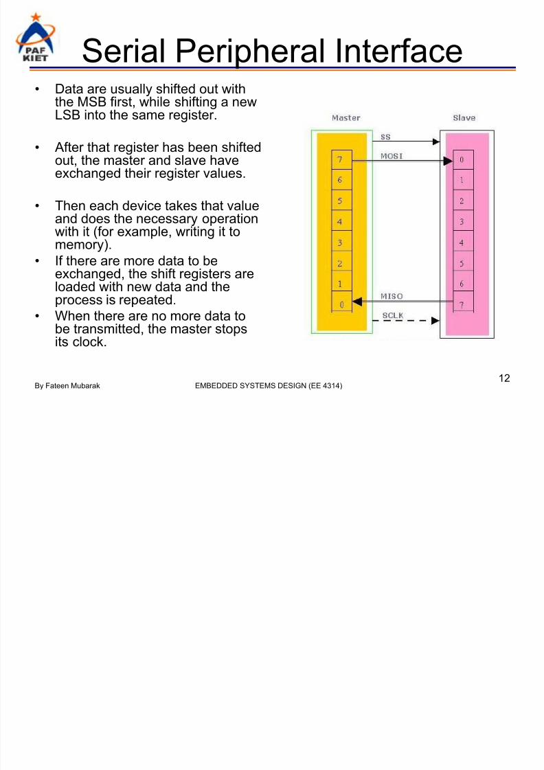
Serial Peripheral Interface•
Data are usually shifted out withthe MSB first, while shifting a newLSB into the same register.
• After that register has been shiftedout, the master and slave haveexchanged their register values.
• Then each device takes that valueand does the necessary operationwith it (for example, writing it tomemory).
• If there are more data to beexchanged, the shift registers are
loaded with new data and theprocess is repeated.
• When there are no more data tobe transmitted, the master stopsits clock.
8/12/2019 embedded system session 8
http://slidepdf.com/reader/full/embedded-system-session-8 13/19
By Fateen Mubarak EMBEDDED SYSTEMS DESIGN (EE 4314) 1313
Serial Peripheral Interface

8/12/2019 embedded system session 8
http://slidepdf.com/reader/full/embedded-system-session-8 14/19
By Fateen Mubarak EMBEDDED SYSTEMS DESIGN (EE 4314) 14
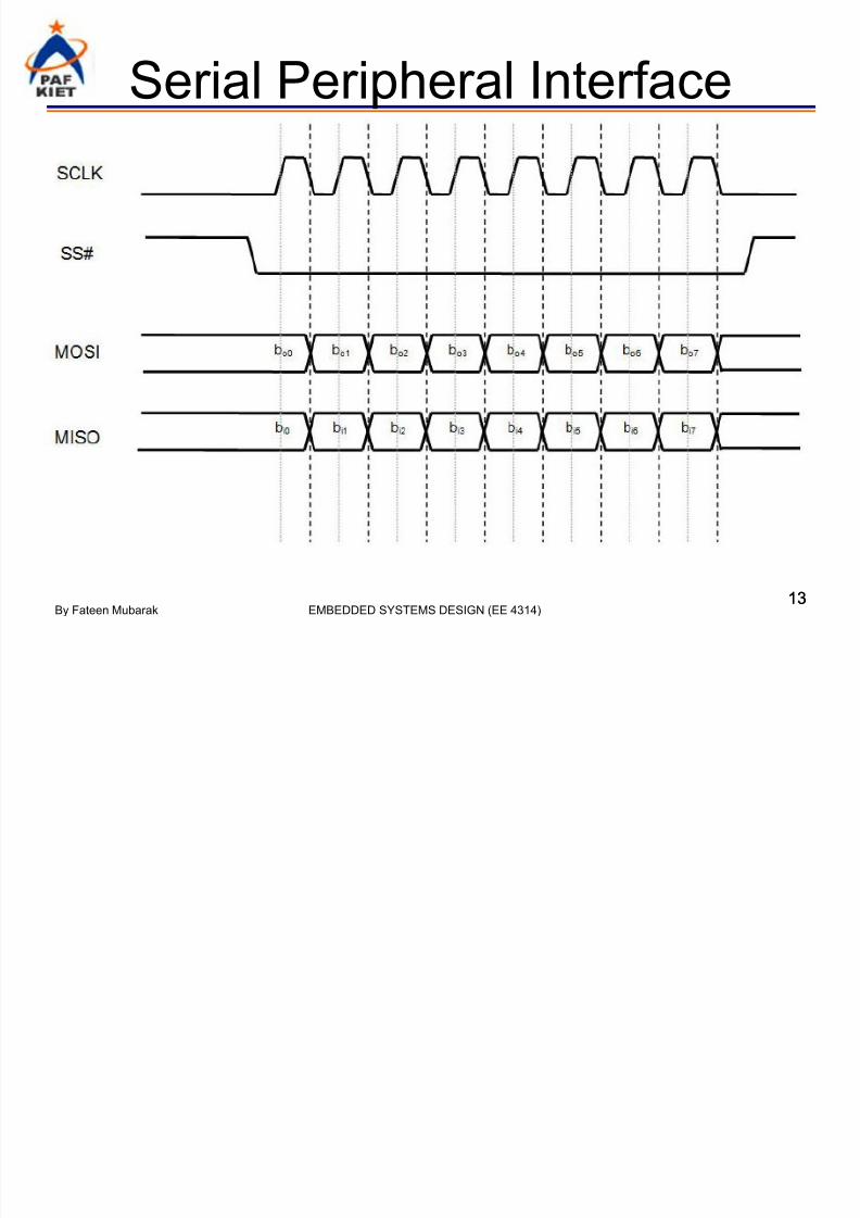
Serial Peripheral Interface
• Data Bits on MOSI and MMISO toggle on
the SCLK falling edge and are sampled on
the SCLK rising edge.
• SPI mode defines which SCLK edge is
used for toggling data and which SCLK
edge is used for sampling data
14

8/12/2019 embedded system session 8
http://slidepdf.com/reader/full/embedded-system-session-8 15/19
By Fateen Mubarak EMBEDDED SYSTEMS DESIGN (EE 4314) 15
Serial Peripheral Interface
15
Clock polarity (CPOL) and clock phase (CPHA) are the main
parameters that define a clock format to be used by the SPI bus
If CPHA=0 the data are sampled on the leading (first) clock edge.If CPHA=1 the data are sampled on the trailing (second) clock
edge,
8/12/2019 embedded system session 8
http://slidepdf.com/reader/full/embedded-system-session-8 16/19
By Fateen Mubarak EMBEDDED SYSTEMS DESIGN (EE 4314) 16
Serial Peripheral Interface
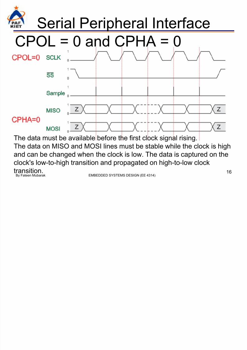
CPOL = 0 and CPHA = 0
The data must be available before the first clock signal rising.
The data on MISO and MOSI lines must be stable while the clock is high
and can be changed when the clock is low. The data is captured on the
clock's low-to-high transition and propagated on high-to-low clock
transition.

8/12/2019 embedded system session 8
http://slidepdf.com/reader/full/embedded-system-session-8 17/19
By Fateen Mubarak EMBEDDED SYSTEMS DESIGN (EE 4314) 17
Serial Peripheral Interface
17
CPOL = 0 and CPHA = 1
The data on MISO and MOSI lines must be stable while the clock is low
and can be changed when the clock is high. The data is captured on the
clock's high-to-low transition and propagated on low-to-high clock
transition

8/12/2019 embedded system session 8
http://slidepdf.com/reader/full/embedded-system-session-8 18/19
By Fateen Mubarak EMBEDDED SYSTEMS DESIGN (EE 4314) 18
Serial Peripheral Interface
18
CPOL = 1 and CPHA = 0
The data must be available before the first clock signal falling.
The data on MISO and MOSI lines must be stable while the clock is low and
can be changed when the clock is high. The data is captured on the clock's
high-to-low transition and propagated on low-to-high clock transition

8/12/2019 embedded system session 8
http://slidepdf.com/reader/full/embedded-system-session-8 19/19
By Fateen Mubarak EMBEDDED SYSTEMS DESIGN (EE 4314) 19
Serial Peripheral Interface
19
CPOL = 1 and CPHA = 1
The data on MISO and MOSI lines must be stable while the clock is high and
can be changed when the clock is low.
The data is captured on the clock's low-to-high transition and propagated on
high-to-low clock transition


