Embedded Systems Design, Prof. Kasim Alaubidy Embedded Systems Design (0630470) Lecture 11 Microcontroller Interfacing Microcontroller Interfacing Microcontroller Interfacing Microcontroller Interfacing Prof. Kasim M. Al-Aubidy Philadelphia University-Jordan
Transcript
Embedded Systems Design,Prof. Kasim Alaubidy
Embedded Systems Design(0630470)
Lecture 11
Microcontroller InterfacingMicrocontroller InterfacingMicrocontroller InterfacingMicrocontroller InterfacingProf. Kasim M. Al-Aubidy
- It is supplied in an 18-pic DIL chip.- Some of the pins have dual functions.- It has TWO ports, Port A & Port B.- A summary of the pin functions is provided inthe next table.
Embedded Systems Design,Prof. Kasim Alaubidy
Embedded Systems Design,Prof. Kasim Alaubidy
• NOTES:- Timer Zero Register (TMR0): File Register # 01- Program Counter: File Register # 02- Status or Flag Register: File Register # 03
- Port A Data Register: File Register # 05- Port B Data Register: File Register # 06- Interrupt Control Register (INTCON): File Register # 0B- General Purpose Register 1: File Register # 0C- General Purpose Register 2: File Register # 0D
..
- General Purpose Register 68: File Register # 4F
- Working Register: W register: it is 8-bit data register used to hold data that is currently being worked.It is separate from the file register set.
- W register and General Purpose Registers are in RAM Bank (bank 0). These registers can be directlyaccessed.
- Bank 1 Registers (TRISA, TRISB and PCLATH) can not be directly accessed. In this case, specialinstructions are needed to load them. There are TWO ways to do this:
1. Simple Method: it requires the 8-bit code to be loaded to be placed in W first, and then moved intoBank 1.
2. Bank Selection Method: using operation BANKSEL which selects the bank that the specified registeris in.
Embedded Systems Design,Prof. Kasim Alaubidy
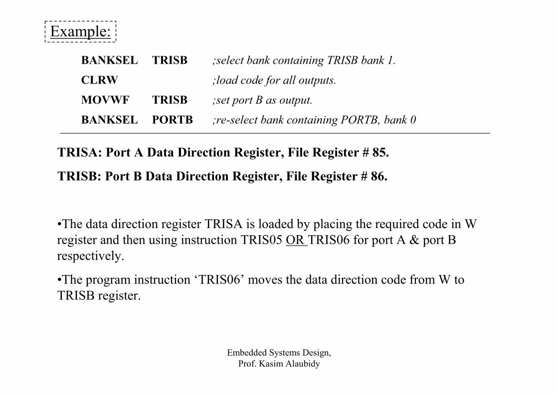
Example:
;re-select bank containing PORTB, bank 0PORTBBANKSEL
;set port B as output.TRISBMOVWF
;load code for all outputs.CLRW
;select bank containing TRISB bank 1.TRISBBANKSEL
TRISA: Port A Data Direction Register, File Register # 85.
TRISB: Port B Data Direction Register, File Register # 86.
•The data direction register TRISA is loaded by placing the required code in Wregister and then using instruction TRIS05 OR TRIS06 for port A & port Brespectively.
•The program instruction ‘TRIS06’ moves the data direction code from W toTRISB register.
Embedded Systems Design,Prof. Kasim Alaubidy
STATUS: Status or flag register : File Register #03
Embedded Systems Design,Prof. Kasim Alaubidy
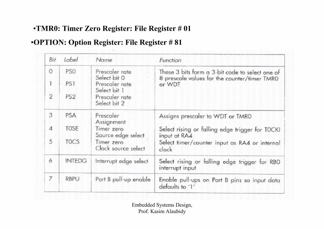
•OPTION: Option Register: File Register # 81
•TMR0: Timer Zero Register: File Register # 01
Embedded Systems Design,Prof. Kasim Alaubidy
•INTCON: Interrupt control Register: File Register # 0B
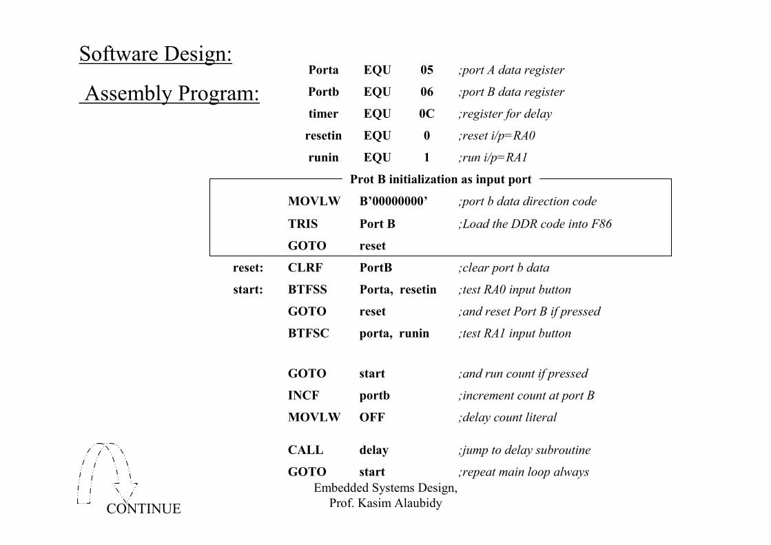
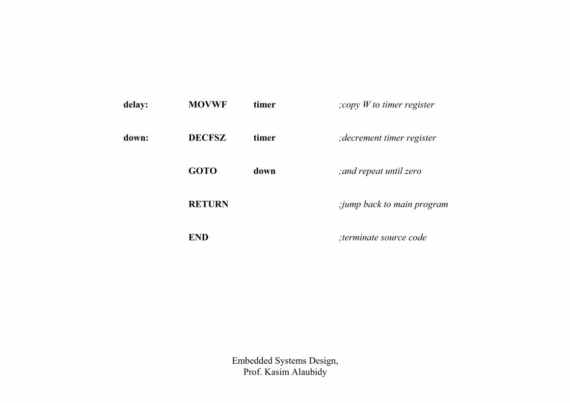
Design a PIC-based system that displays a binary count of asequence of pulses under the control of two push button switches.One input will start the output sequence when pressed. The otherinput will clear the output.