15
© 2018 ROHM Co.,Ltd. ROHM Co. Ltd. EMC Basics ver.A2 Reprinting forbidden
© 2018 ROHM Co.,Ltd.
ROHM Co. Ltd.
EMC Basics
ver.A2
Reprinting forbidden
P. 1© 2018 ROHM Co.,Ltd.
Reprinting forbiddenAgenda
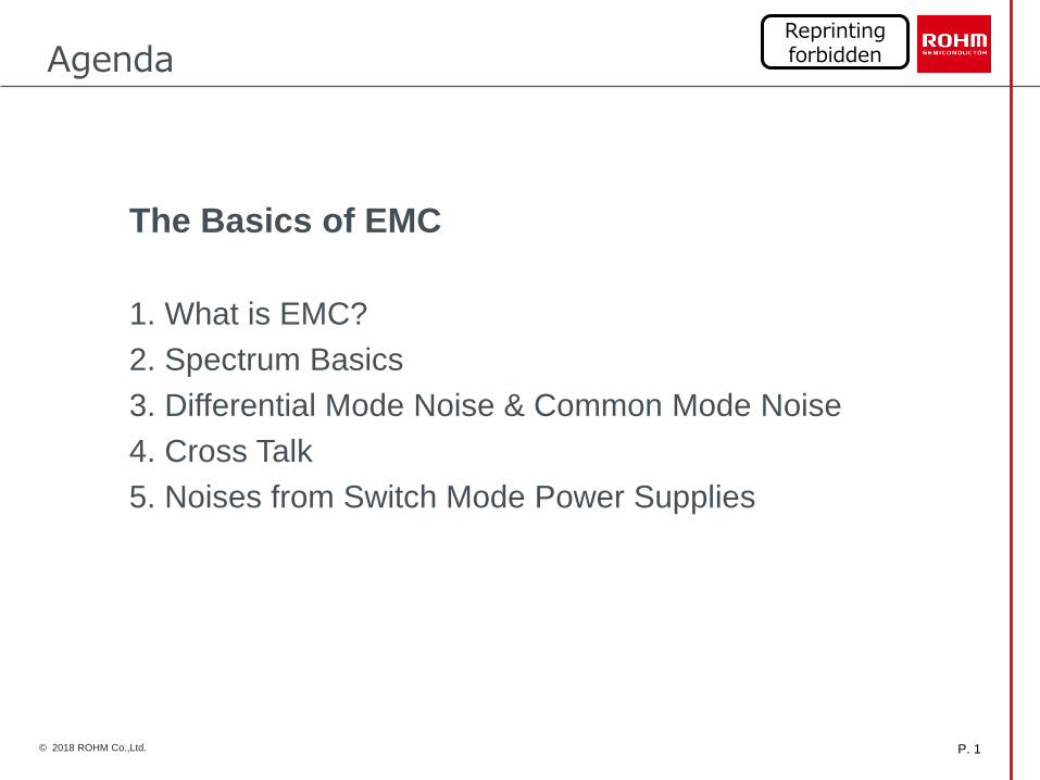
The Basics of EMC
1. What is EMC?
2. Spectrum Basics
3. Differential Mode Noise & Common Mode Noise
4. Cross Talk
5. Noises from Switch Mode Power Supplies
P. 2© 2018 ROHM Co.,Ltd.
Reprinting forbidden1. What is EMC?
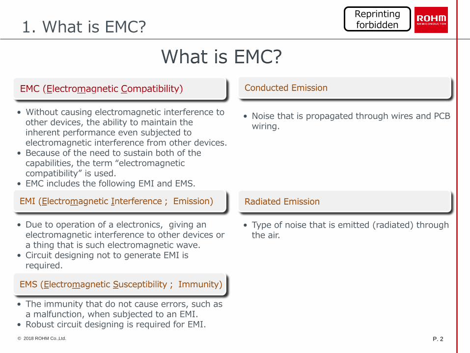
What is EMC?
• Without causing electromagnetic interference to other devices, the ability to maintain the inherent performance even subjected to electromagnetic interference from other devices.
• Because of the need to sustain both of the capabilities, the term “electromagnetic compatibility” is used.
• EMC includes the following EMI and EMS.
EMI (Electromagnetic Interference; Emission)
• Due to operation of a electronics, giving an electromagnetic interference to other devices or a thing that is such electromagnetic wave.
• Circuit designing not to generate EMI is required.
EMS (Electromagnetic Susceptibility; Immunity)
• The immunity that do not cause errors, such as a malfunction, when subjected to an EMI.
• Robust circuit designing is required for EMI.
Conducted Emission
Radiated Emission
• Noise that is propagated through wires and PCB wiring.
• Type of noise that is emitted (radiated) through the air.
P. 3© 2018 ROHM Co.,Ltd.
Reprinting forbidden2. Spectrum Basics
f
dB
πtw
-20dB/dec
-40dB/dec
πts
ts ts
T
A
A tw
2
1 1
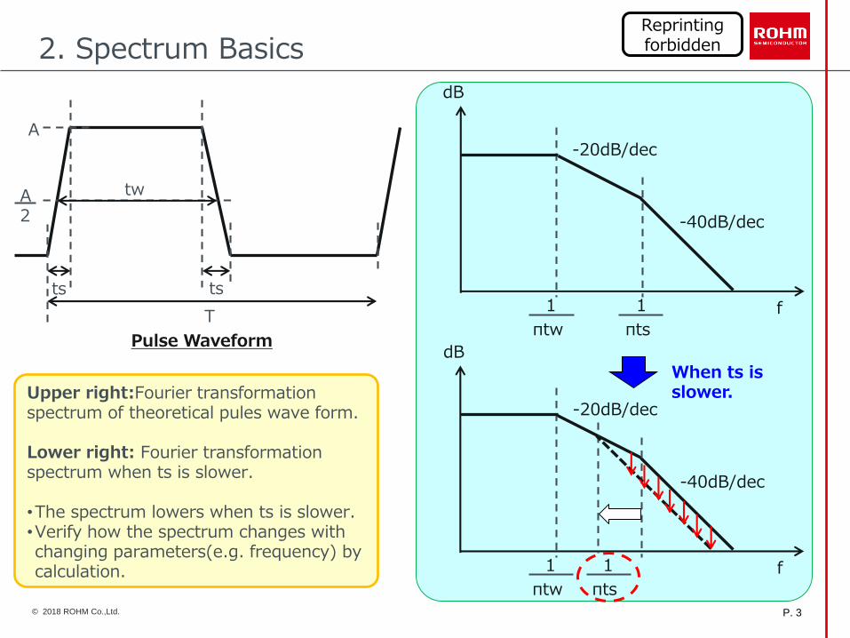
Upper right:Fourier transformation spectrum of theoretical pules wave form.
Lower right: Fourier transformation spectrum when ts is slower.
•The spectrum lowers when ts is slower.•Verify how the spectrum changes with changing parameters(e.g. frequency) by calculation.
Pulse Waveform
f
dB
πtw
-20dB/dec
-40dB/dec
πts
1 1
When ts is slower.
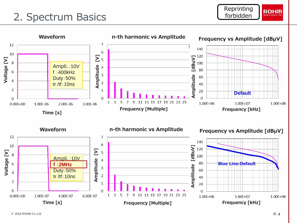
P. 4© 2018 ROHM Co.,Ltd.
Reprinting forbidden
Ampli.:10V
f :400kHz
Duty:50%
tr /tf:10ns
Default
Ampli.:10V
f :2MHz
Duty:50%
tr /tf:10ns
Blue Line:Default
2. Spectrum Basics
Volt
ag
e [
V]
Am
plitu
de [V
]
Am
plitu
de [d
Bu
V]
Waveform
Waveform
n-th harmonic vs Amplitude
n-th harmonic vs Amplitude
Frequency vs Amplitude [dBµV]
Frequency [kHz]
Frequency [kHz]
Frequency [Multiple]
Frequency [Multiple]
Time [s]
Time [s]
Volt
ag
e [
V]
Am
plitu
de [V
]
Frequency vs Amplitude [dBµV]
Am
plitu
de [d
Bu
V]
P. 5© 2018 ROHM Co.,Ltd.
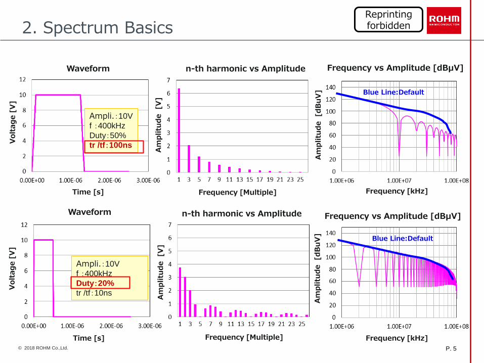
Reprinting forbidden2. Spectrum Basics
Ampli.:10V
f :400kHz
Duty:50%
tr /tf:100ns
Blue Line:Default
Ampli.:10V
f :400kHz
Duty:20%
tr /tf:10ns
Blue Line:Default
Waveform
Waveform
n-th harmonic vs Amplitude
n-th harmonic vs Amplitude
Frequency vs Amplitude [dBµV]
Frequency [kHz]
Frequency [kHz]
Frequency [Multiple]
Frequency [Multiple]
Time [s]
Time [s]
Volt
ag
e [
V]
Am
plitu
de [V
]
Frequency vs Amplitude [dBµV]
Volt
ag
e [
V]
Am
plitu
de [V
]
Am
plitu
de [d
Bu
V]
Am
plitu
de [d
Bu
V]
P. 6© 2018 ROHM Co.,Ltd.
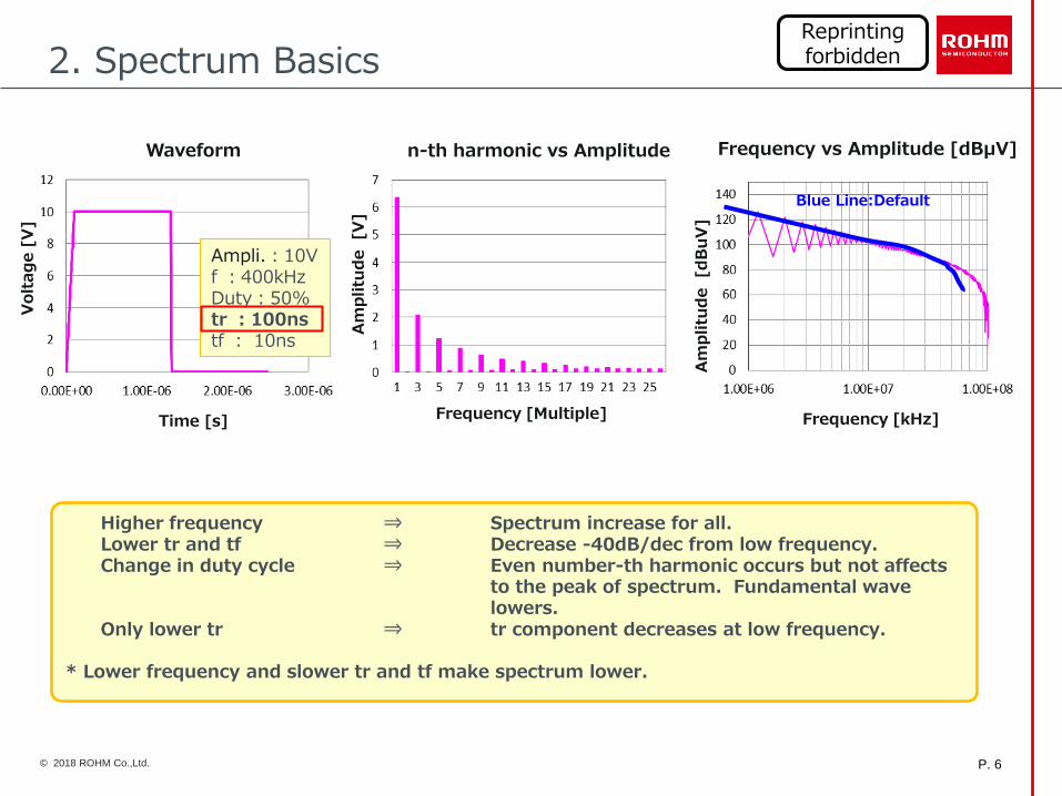
Reprinting forbidden2. Spectrum Basics
Higher frequency ⇒ Spectrum increase for all.Lower tr and tf ⇒ Decrease -40dB/dec from low frequency.Change in duty cycle ⇒ Even number-th harmonic occurs but not affects
to the peak of spectrum. Fundamental wave lowers.
Only lower tr ⇒ tr component decreases at low frequency.
* Lower frequency and slower tr and tf make spectrum lower.
Ampli.:10Vf :400kHzDuty:50%tr :100nstf : 10ns
Blue Line:Default
Waveform n-th harmonic vs Amplitude Frequency vs Amplitude [dBµV]
Frequency [kHz]Frequency [Multiple]Time [s]
Volt
ag
e [
V]
Am
plitu
de [V
]
Am
plitu
de [d
Bu
V]
P. 7© 2018 ROHM Co.,Ltd.
Reprinting forbidden3. Differential Mode Noise & Common Mode Noise
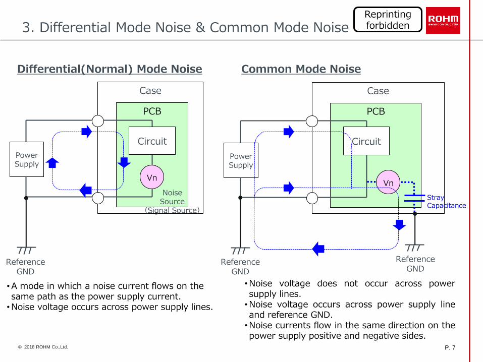
Case
PCB
Circuit
PowerSupply
Differential(Normal) Mode Noise Common Mode Noise
Reference GND
•A mode in which a noise current flows on the same path as the power supply current.•Noise voltage occurs across power supply lines.
•Noise voltage does not occur across powersupply lines.•Noise voltage occurs across power supply lineand reference GND.•Noise currents flow in the same direction on thepower supply positive and negative sides.
Case
PCB
Circuit
PowerSupply
Reference GND
Stray Capacitance
VnVn
NoiseSource
(Signal Source)
Reference GND
P. 8© 2018 ROHM Co.,Ltd.
Reprinting forbidden
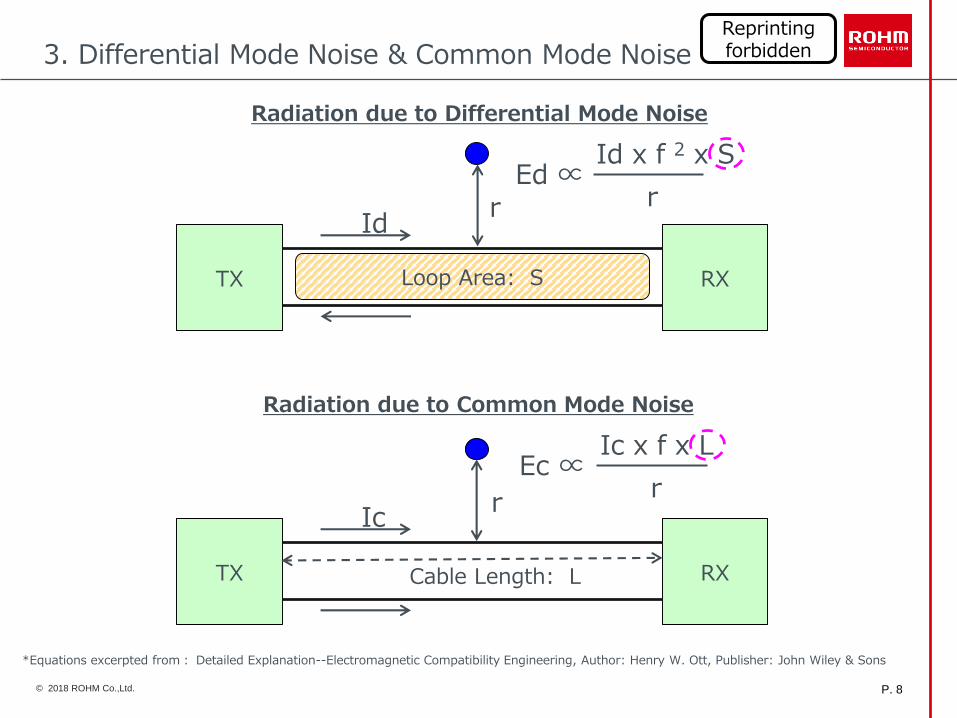
TX RXLoop Area: S
rId
Radiation due to Differential Mode Noise
Ed ∝ Id x f 2 x S
r
TX RX
Ic
Radiation due to Common Mode Noise
Cable Length: L
r
Ec ∝ Ic x f x L
r
*Equations excerpted from: Detailed Explanation--Electromagnetic Compatibility Engineering, Author: Henry W. Ott, Publisher: John Wiley & Sons
3. Differential Mode Noise & Common Mode Noise
P. 9© 2018 ROHM Co.,Ltd.
Reprinting forbidden
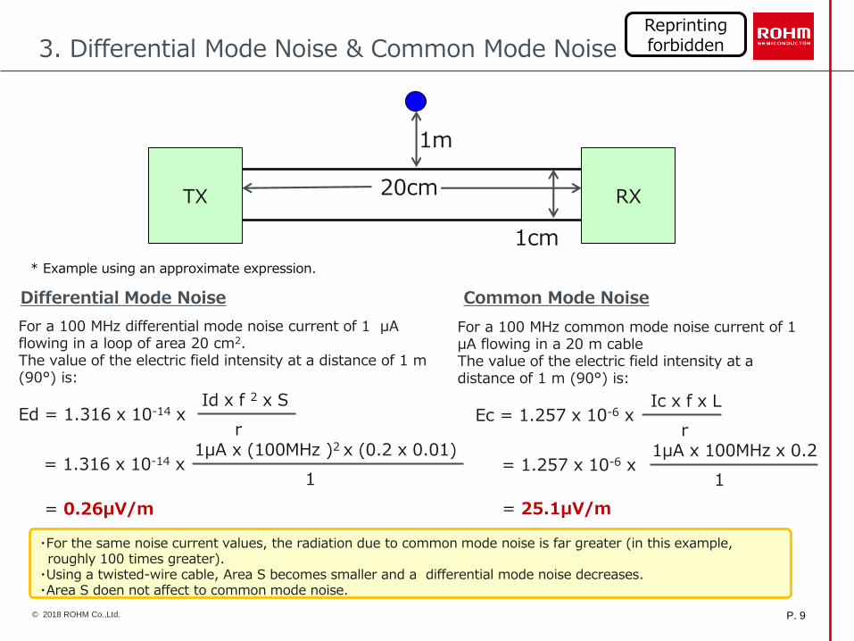
For a 100 MHz differential mode noise current of 1 µA flowing in a loop of area 20 cm2.The value of the electric field intensity at a distance of 1 m (90°) is:
Ed = 1.316 x 10⁻¹⁴ x Id x f 2 x S
r
= 1.316 x 10-14 x 1µA x (100MHz )2 x (0.2 x 0.01)
1
= 0.26µV/m
Differential Mode Noise
For a 100 MHz common mode noise current of 1 µA flowing in a 20 m cableThe value of the electric field intensity at a distance of 1 m (90°) is:
Ec = 1.257 x 10⁻⁶ x Ic x f x L
r
= 1.257 x 10-6 x 1µA x 100MHz x 0.2
1
= 25.1µV/m
Common Mode Noise
* Example using an approximate expression.
TX RX20cm
1cm
1m
・For the same noise current values, the radiation due to common mode noise is far greater (in this example, roughly 100 times greater).
・Using a twisted-wire cable, Area S becomes smaller and a differential mode noise decreases.・Area S doen not affect to common mode noise.
3. Differential Mode Noise & Common Mode Noise
P. 10© 2018 ROHM Co.,Ltd.
Reprinting forbidden4. Crosstalk
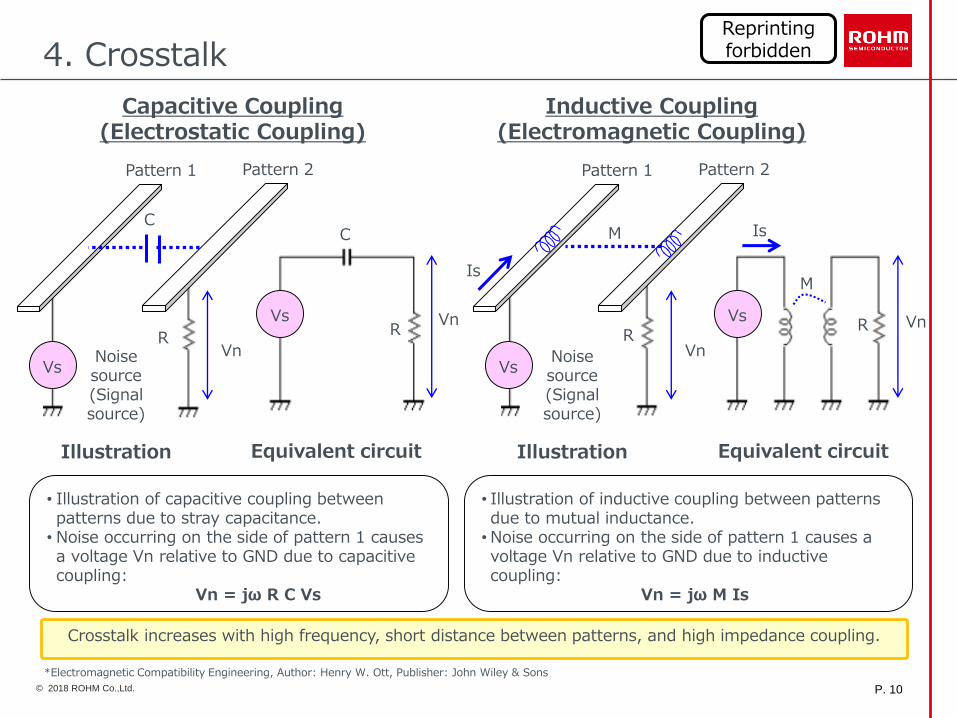
Crosstalk increases with high frequency, short distance between patterns, and high impedance coupling.
Capacitive Coupling(Electrostatic Coupling)
Inductive Coupling (Electromagnetic Coupling)
VsVn
Pattern 1
R
CC
R
Pattern 2
Vs Vn
Illustration Equivalent circuit
• Illustration of capacitive coupling between patterns due to stray capacitance.
• Noise occurring on the side of pattern 1 causes a voltage Vn relative to GND due to capacitive coupling:
Vn = jω R C Vs
• Illustration of inductive coupling between patterns due to mutual inductance.•Noise occurring on the side of pattern 1 causes a voltage Vn relative to GND due to inductive coupling:
Vn = jω M Is
Noise source (Signal source)
VsVn
Pattern 1
R
Pattern 2
M
IsM
Is
Vs Vn
Illustration Equivalent circuit
Noise source (Signal source)
R
*Electromagnetic Compatibility Engineering, Author: Henry W. Ott, Publisher: John Wiley & Sons
P. 11© 2018 ROHM Co.,Ltd.
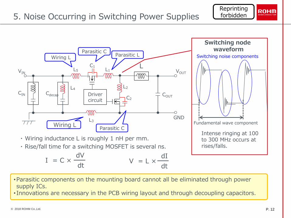
Reprinting forbidden5. Noise Occurring in Switching Power Supplies
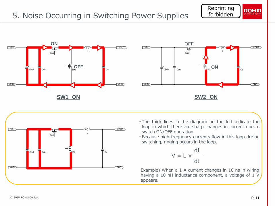
ON
OFF
SW1 ON
OFF
ON
SW2 ON
• The thick lines in the diagram on the left indicate theloop in which there are sharp changes in current due toswitch ON/OFF operation.
• Because high-frequency currents flow in this loop duringswitching, ringing occurs in the loop.
dI
dtV = L ×
Example) When a 1 A current changes in 10 ns in wiringhaving a 10 nH inductance component, a voltage of 1 Vappears.
P. 12© 2018 ROHM Co.,Ltd.
Reprinting forbidden
•Parasitic components on the mounting board cannot all be eliminated through power supply ICs.• Innovations are necessary in the PCB wiring layout and through decoupling capacitors.
V = L ×dt
dI
LVIN
Driver circuit
CIN Cdecap
VOUTL5 L1
L2
L3
L4
Parasitic C
COUT
Parasitic C
Wiring LParasitic L
Wiring L
Intense ringing at 100 to 300 MHz occurs at rises/falls.
Switching node waveform
GND
C1
C2
・ Wiring inductance L is roughly 1 nH per mm.
・ Rise/fall time for a switching MOSFET is several ns.
I = C ×dt
dV
Fundamental wave component
Switching noise components
5. Noise Occurring in Switching Power Supplies
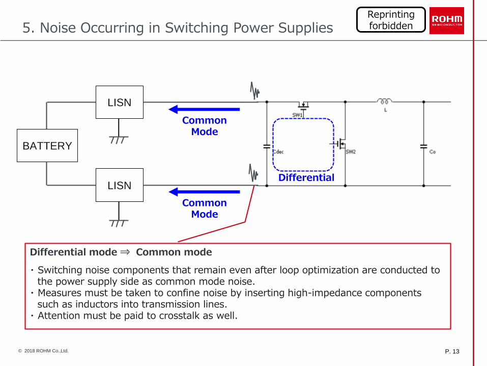
P. 13© 2018 ROHM Co.,Ltd.
Reprinting forbidden
BATTERY
LISN
LISN
Common Mode
Common Mode
Differential
Differential mode ⇒ Common mode
・ Switching noise components that remain even after loop optimization are conducted to the power supply side as common mode noise.
・ Measures must be taken to confine noise by inserting high-impedance components such as inductors into transmission lines.
・ Attention must be paid to crosstalk as well.
5. Noise Occurring in Switching Power Supplies
© 2018 ROHM Co.,Ltd.


