EMC Compliant, Isolated, 2-Channel Binary or Digital Input Module for WideAC/DC Input Reference Design
TI DesignsEMC Compliant, Isolated, 2-Channel Binary or Digital InputModule for Wide AC/DC Input Reference Design
All trademarks are the property of their respective owners.
DescriptionThis TI Design showcases a cost optimizedarchitecture that improves resolution of an AC or DCbinary input module. A microcontroller unit (MCU) isshared between two input channels (group isolation) tooptimize the cost per channel. Wide input range iscovered using an amplifier with gain and an MCUintegrated 10-bit analog-to-digital converter (ADC) tomeasure within ±3% accuracy. This architectureeliminates the need for multiple hardware versionsbased on input voltage range as is the case with anoptocoupler based topology. A digital isolator is usedto communicate the ADC code or the root-mean-square value of the input to the host processor. Thedesign is tested for ESD, EFT, and surge as perIEC61000-4 Level 4.
Features• MSP430™ Family MCU Based 2-Channel AC/DC
Voltage Measurement Module With Low PowerConsumption
• Isolated Interface Between Binary Module and HostMCU
• Binary Module Design Based on Basic orReinforced Digital Isolator With High or Low DefaultOutput
• LMV614 Op Amp Based Gain Stages for ImprovedMeasurement Accuracy (×1 and ×3.5)
• Stable Reference for DC Level Shifting InputsGenerated by LM4041 and Buffered Using LMV551
• Accuracy ≤ ±3% of Measured Value ±1 V(Programming Resolution or Step Size)
• Accurate Measurement of Input Voltage Over WideTemperature Range
• Measurement Resolution Less Than 1 V• Inputs Rated up to 300-V AC/DC• >300-kΩ Impedance for Binary Input• Less Than 1-mA Consumption at 276-V Input• Tested for ESD, EFT and Surge as per IEC61000-
4 Standard Requirements for Pre-Compliance• PCB Width ≤ 1 inch
Applications• Multifunction Protection Relay• Substation Bay Controller and Battery Monitoring• RTU / FTU / DTU / FRTU• Merging Unit• PLC Digital Input Module
EMC Compliant, Isolated, 2-Channel Binary or Digital Input Module for WideAC/DC Input Reference Design
An IMPORTANT NOTICE at the end of this TI reference design addresses authorized use, intellectual property matters and otherimportant disclaimers and information.
1 System Overview
1.1 System Description
1.1.1 Introduction to IED and Subsystems in Grid Applications
Figure 1. Generic Block Diagram of a Protection Relay
The protection relay, intelligent electronic device (IED), or substation controllers used in grid applicationshave the following generic subsystems. The subsystems are based on the functionality and are as follows:• CPU or DSP module
– This module handles all protection functions and logic. Additionally, the HMI and communicationfunctions are also handled by this module.
• Power supply– Nominal auxiliary voltage: 24-V DC, 48- to 60-V DC, 110- to 125-V DC, 220-V DC, and 230-V AC,
50 or 60 Hz, ± 20%, and 40-W max. admissible consumption– Stored energy for up to 50 ms power supply interruption
• AC measurement inputs– Nominal frequency (FNOM): 50 or 60 Hz
• CT measurements inputs– Nominal current: 1 or 5 A (ΙN)
• VT measurement inputs– Nominal voltage: 57.7 to 500 V– Maximum measurable voltage: 577 VRMS
EMC Compliant, Isolated, 2-Channel Binary or Digital Input Module for WideAC/DC Input Reference Design
• DC analog input range (independently configurable):– ±1.25, ±2.5, ±5, and ±10 V– ±1, ±5, ±10, and ±20 mA– 0 to 1, 0 to 5, 0 to 10, 0 to 20, and 4 to 20 mA
• DC analog output range (independently configurable):– ±5, ±10, ±20 mA, and 4 to 20 mA
• Digital inputs– Nominal voltage: 24-V DC, 48- to 60-V DC, 110- to 125-V DC/AC and 220-V DC/AC, ±20% or
multi-voltage (24 to 250-V DC/AC)– Power consumption per input: 2 to 6 mA, maximum power dissipation is 0.45 W ±20% per input or
short peak-current (> 25 mA)– Groups of 4, 8, 12, 16, or 32
• Digital output relays– Continuous current: 5 A
• Control output relays– Continuous current: 5 A
• Time synchronization– by an IRIG–B GPS clock (through the IRIG-B input)– by an Ethernet SNTP server– by a time telegram message issued by remote Scada (DNP3.0, IEC 60870-5-101 or
IEC 60870-5-104)• Communication capabilities
– Ethernet communication• 10/100BASE-TX, auto-crossing or 100BASE-FX• Embedded Ethernet switch module with up to six ports (permitting a compact connection of
various devices or I/O extensions)– Serial communication
• Up to two SCADA or four IED links per device• SCADA protocol can be switched between DNP3.0, IEC 60870-5-101 and MODBUS• IED Protocol can be switched between DNP3.0, IEC 60870-5-103, MODBUS and
IEC 60870-5-101
This TI Design focuses on designing a digital input module to measure a wide AC/DC input withprogrammable threshold with digital isolators.
1.1.2 Binary or Digital InputsThe inputs to the protection relay or substation controllers are called under different names:• Binary input• Digital input• Control input• Indication input
These names are based on the function performed. This design guide will refer to these inputs as binaryinputs. Binary inputs have wide applications. The binary input module specifications differ with OEMs. Thebinary inputs are designed as modules and, based on the application, one or more modules are used. Thefollowing subsections detail some of these applications, functionalities, and specifications. These inputshave galvanic isolation from internal circuits; generally, optocouplers are used for isolation. The number ofbinary inputs per module can vary as 4, 8, 16, or 32. The binary inputs are organized in groups(depending upon application) with a common wire. In some of the applications, the inputs are channelisolated.
EMC Compliant, Isolated, 2-Channel Binary or Digital Input Module for WideAC/DC Input Reference Design
1.1.2.1 Binary Input ApplicationsSome grid applications use binary inputs for the following functionalities:• Substation battery monitoring• Bay or substation interlocking• Breaker status indication• General interrogations• LED test• Diagnostics (self-test)• Fault indication (alarm)• Configuration change (operated with new settings to perform different functionality)
1.1.2.2 Binary Input SpecificationsKey specifications include:• Input voltage range• Threshold for guaranteed operation• Response or reset time (software provides de-bounce time)• Power consumption, energized
General specifications include:• Inputs are jumper selectable for low range (nominal system voltages of up to 100 V) or high range
(from 100 to 300 V)• Tolerance: ±10%• Common input voltage ranges:
– 24-V DC– 48-V DC– 110-V AC/DC– 230-V AC/DC
• Frequency: 50 or 60 Hz• Contacts per common return: Four or more• Recognition (processing of the inputs) time: ≥ 20 ms• Inputs protected against continuous overload up to 300-V AC/DC• All I/O terminals protected with internal transient limiting devices• Continuous current draw: < 5 mA• Auto-burnish impulse current: 20 to 50 mA• Duration of auto-burnish impulse: 25 to 50 ms
1.1.2.3 Wetting or Auto BurnishingThe binary inputs sense a change of the state of the external device. When these external devices are inharsh industrial environments (either outdoor or indoor), their contacts can be exposed to various types ofcontamination. Normally, there is a thin film of insulating sulfidation, oxidation, or contaminates on thesurface of the contacts, sometimes making it difficult or impossible to detect a change of the state. Thisfilm must be removed to establish circuit continuity; an impulse of higher than normal current canaccomplish this.
The contact inputs with auto-burnish create a high current impulse when the threshold is reached to burnoff this oxidation layer as maintenance to the contacts. Afterwards, the contact input current is reduced toa steady-state current. Contact inputs with auto burnishing allow currents up to 50 mA at the first instancewhen the change of state was sensed. Then, within 25 to 50 ms, this current is slowly reduced to 5 mA.The 50-mA peak current burns any film on the contacts, allowing for proper sensing of state changes.
EMC Compliant, Isolated, 2-Channel Binary or Digital Input Module for WideAC/DC Input Reference Design
1.1.2.4 Miscellaneous FeaturesFilters prevent the input signal from being detected erroneously. The following types of input filters can beused:• The hardware input filter is used to suppress contact bounce (1 to 64 ms).• Change-of-state delay is used to suppress short signal interruptions.• Chatter blocking is used to suppress huge bursts of indications in case of defective battery or
intermediate relays.
1.1.3 Isolation
Table 1. Key Methods of Isolation
SiO2: ISO72x; Typical BV is VPEAK/µm• Inorganic• Highly stable (over temperature, moisture, time), high quality• Used extensively and for a long time as dielectric in semiconductor (low defunct rates)• Deposited in a controlled semiconductor process
Polymide: ADI transformer core; Typical BV is 250 VPEAK/µm• Organic• Retains moisture — affects lifetime especially at high voltages• Used in semiconductor mainly for stress relief and now as isolation barrier
Epoxy: Optocouplers; Typical BV is 50 VPEAK/µm• Uses filler materials• Leaky (higher partial discharge)• Applied at packaging as mold compound• Voids and anomalies are common
1.1.4 EMC—Transient Overvoltage StressIn industrial applications, lightning strikes, power source fluctuations, inductive switching, and electrostaticdischarge (ESD) can cause damage to binary inputs by generating large transient voltages. The followingESD and surge protection specifications are relevant to binary input applications:• IEC 61000-4-2 ESD• IEC 61000-4-4 EFT• IEC 61000-4-5 Surge
The level of protection can be further enhanced when using external clamping devices such as TVSdiodes. The transients are clamped instantaneously (< 1 ns), and the damaging current is diverted awayfrom the protected device.
1.1.5 TI Design AdvantagesSome of the advantage of the AC/DC binary input module is as follows:• Provides isolation using digital isolator with basic or reinforced isolation and increased reliability• Costs optimized solution with option for expansion up to four digital inputs• Allows for measurement of wide AC/DC input voltage• Uses MCU to allow flexibility in terms of input voltage processing, measurement accuracy and control
of wetting current• Reduces measurement error caused due to bridge rectifier at the input (no bridge rectifier used)• Improves voltage input measurement accuracy by using multiple gain stages• Provides provision for programmable threshold on the host side
EMC Compliant, Isolated, 2-Channel Binary or Digital Input Module for WideAC/DC Input Reference Design
1.2 Key System SpecificationsThe AC/DC binary module measures the input voltage in terms of ADC counts. To ensure wide inputAC/DC voltages are measured within the required accuracy, two gain stages have been used for eachinput: high gain and low gain. ADC counts after subtracting the DC offset is averaged for 10 or 30 ms.ADC counts for each channel (high and low) are communicated to the host. The host converts the ADCcount into voltage for further processing. The conversion factor changes for DC and AC voltages. Theconversion factor also changes for high gain and low gain.
EMC Compliant, Isolated, 2-Channel Binary or Digital Input Module for WideAC/DC Input Reference Design
1.3 Block DiagramThis TI Design provides an innovative and cost optimized method to measure the digital input accuratelyover wide temperature and input using the MSP430 family of MCUs and high reliability digital isolators.Digital isolators are used to provide the required isolation between the digital input processing circuit andthe host MCU. The design provides the following options:1. Interface to the host interface using digital isolators with basic isolation (BI)2. Interface to the host interface using digital isolators with reinforced isolation (RI)
The DC or AC inputs are applied across potential divider and the divider output is amplified by ×1 or ×3.5gain, and the MCU converts the analog input to 10-bit digital value that is used for computing the RMSvoltage. The AC input is DC level shifted by VCC/2 for the SAR ADC internal to the MCU using anexternal reference and buffer. The outputs are communicated to the host through digital isolator. Theisolated power supply required for the binary module operation is generated onboard using the SN6501transformer driver. The transformer used in this design is a larger footprint transformer with isolation ratingup to 6 kVRMS.
This TI Design has the following functional blocks:• Potential divider: Divides the input voltage to within the ADC range for measurement including the gain
stage• Operational amplifier (op amp) gain: Covers the wide AC/DC input over wide range, two gain stages
are used. A higher gain amplifier stage is used to measure lower input voltages, and for higher inputvoltage, a lower gain amplifier is used.
• Wetting current control: MOSFET-based wetting current control circuit with 2.5K impedance is used.The wetting circuit makes use of the resistors short time over voltage with stand capability for testing.
• MCU: Measures the binary input, controls the wetting current, and communicates the measured inputvalue to the host processor
• Digital isolator: Provides the required isolation between the binary module and the host processor• Power supply: Binary module is powered by 3.3 V from the host side. Isolated power for the binary
module is generated
The TI Design has two boards:• One board has the footprint to mount the smaller package basic isolation digital isolators, named as BI
(board with basic insulation isolator option)• The other board has footprint provision to mount reinforced isolation digital isolators, named as RI
(board with reinforced insulation isolator option)
EMC Compliant, Isolated, 2-Channel Binary or Digital Input Module for WideAC/DC Input Reference Design
1.4 Highlighted Products
1.4.1 MCU With Internal 10-Bit SAR ADCThe MSP430G2332IPW2MSP430 ultra-low-power microcontroller has been considered in this TI Design.The MCU has an internal 10-bit ADC.
Other features include:• Low supply voltage range: 1.8 to 3.6 V• Ultra-low-power consumption
– Active mode: 220 μA at 1 MHz, 2.2 V• Internal very-low-power low-frequency (LF) oscillator• One 16-bit Timer_A with three capture/compare registers
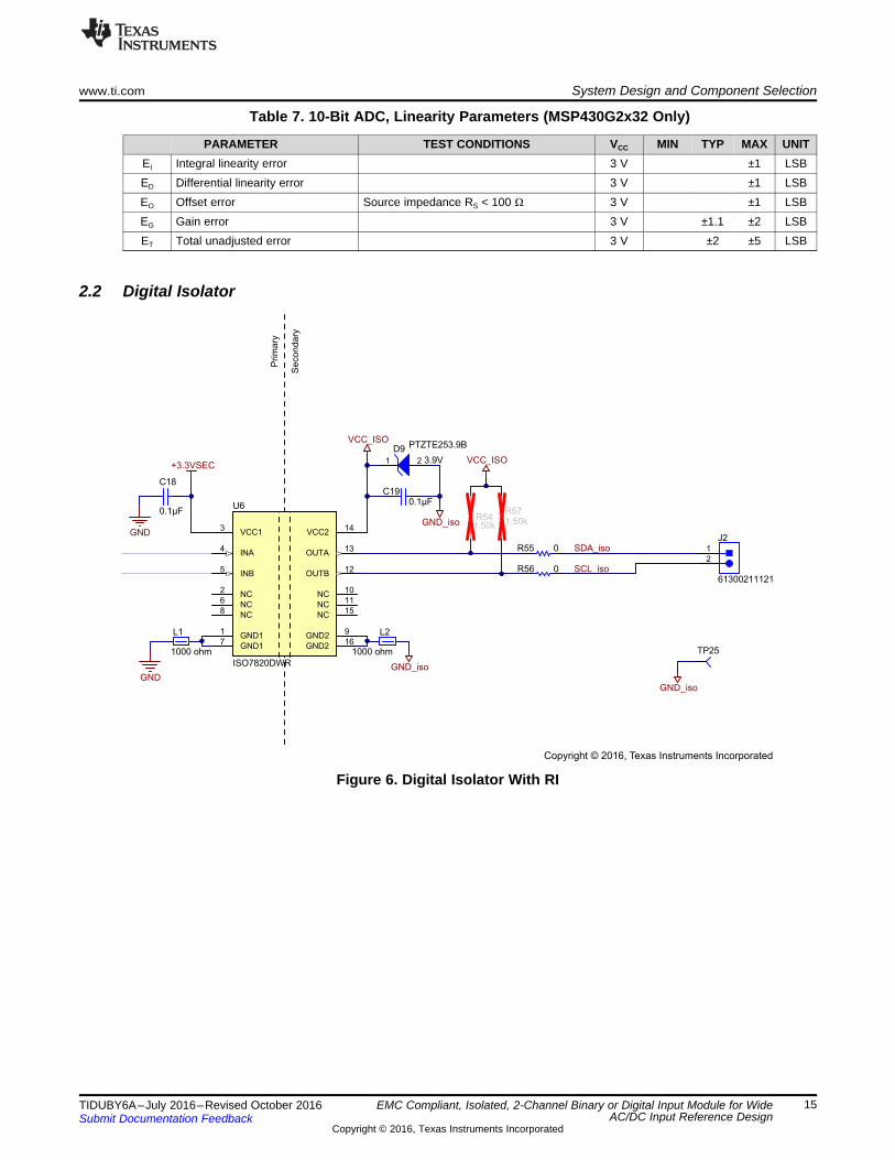
1.4.2 Digital IsolatorDigital isolators are used to provide the required isolation between the binary module and the host MCU.Digital isolators with different isolation options (basic or reinforced) have been tested on the binarymodule.
The ISO1541D provides basic isolation. The ISO1541 has a bidirectional data and a unidirectional clockchannel. The ISO1541 is useful in applications that have a single master. The ISO7320 has two channelsin the same direction and provides basic isolation. The ISO7320FC default output is "low" and theISO7320C default output is "high".
The ISO7820 has two channels in the same direction and provides reinforced isolation. The default outputis high for the ISO7820 and low for the ISO7820F and can be selected based on the application.
Select the isolator depending on the isolation requirements and the EMC levels.
1.4.3 Isolated Power SupplyThe isolated power for the MCU, digital isolator, and the signal conditioning circuit used for sensing thebinary inputs are generated using a push-pull driver for isolated power supplies, the SN6501DBV. Thetransformer used for this application is the 750313638. The transformer package is selected to have anisolation voltage of > 5 kV. Choosing a bigger transformer package facilitates easy migration to reinforcedisolators. Zener diode PTZTE253.9B is used for protecting the power supply against overvoltage andESD. The isolated power supply operates with a single 3.3-V input. The host interface provides therequired power supply for the binary module operation. An LDO TPS70933DBVT is used to improve theADC dynamic range and accuracy of the output supply voltage.
1.4.4 Input Voltage Divider, Signal Conditioning, and Protection• Input protection: TVS SMCJ400CA is used for protecting binary input module against overvoltage and
transients. Package selection is critical to ensure low leakage with temperature variation.• Resistor divider: The AC/DC binary input voltage applied is divided by a resistor divider, which
presents a constant resistance to the binary input. Multiple resistors are used to ensure the resistorswithstand the maximum input voltage reliably. The output of the resistor divider is measured by theADC, and the output voltage range is within the ADC measurement range at maximum input. A Zenerdiode PTZTE255.1B is used to protect the electronic circuit from overvoltage.
• Reference: For measuring AC/DC inputs with internal ADC, the input is level shifted byADC_reference/2. The 1.65-V DC reference is generated using the LM4041. The LMV551 low-powerop amp is used as a buffer for the reference output.
• Gain: To measure wide input AC/DC voltage accurately, an amplifier gain stage is provided. The gainstages are ×1 and ×3.5. These gains are chosen to cover input range of 15 to 276 V. The LMV614amplifier stage is used.
EMC Compliant, Isolated, 2-Channel Binary or Digital Input Module for WideAC/DC Input Reference Design
1.4.5 Wetting Current Control
1.4.5.1 Transistor Drive for MOSFET Gate DriverA transistor is used to drive the MOSFET that controls the wetting current. The bias voltage of 15 V maxfor the MOSFET operation is generated from the binary input using a Zener regulator. The bias current forthe Zener must be in μA and take care when selecting the Zener. Voltage Vz versus Iz characteristics iscritical.
1.4.5.2 Wetting Current Limiting Resistor and MOSFETFour resistors, 10 kΩ each connected in parallel, are used as current limit for wetting current. A D-PAKMOSFET with a 600-V rating AOD2N60A is used that ensures reliability of the MOSFET. The short timeoverload capability of the resistor is being used and take care to not test the wetting current for tests > 100ms (typically 50 ms).
EMC Compliant, Isolated, 2-Channel Binary or Digital Input Module for WideAC/DC Input Reference Design
2 System Design and Component Selection
2.1 MCU With Internal ADCThe binary input modules are cost sensitive, and to ensure the overall solution cost is optimal, an MCUwith an internal ADC has been selected. The internal ADC is a 10-bit SAR ADC.
Figure 4. MCU Functionality Configuration
Texas Instruments’ MSP430 family of ultra-low-power microcontrollers consist of several devices featuringdifferent sets of peripherals targeted for various applications. Combined with five low-power modes, thearchitecture is optimized to achieve an extended battery life in portable measurement applications. Thedevice features a powerful 16-bit RISC CPU, 16-bit registers, and constant generators that contribute tomaximum code efficiency. The digitally controlled oscillator (DCO) allows wake-up from low-power modesto active mode in less than 1 μs.
The MCU considered is the MSP430G2332IPW20. The MSP430G2332IPW20 is an ultra-low-power mixedsignal microcontroller with a built-in 16-bit timer. The device has up to 16 I/O capacitive-touch enabledpins and built-in communication capability using the universal serial communication interface. TheMSP430G2332IPW20 has a 10-bit ADC.
Features:• Low supply voltage range: 1.8 to 3.6 V• Ultra-low power consumption
– Active mode: 220 μA at 1 MHz, 2.2 V– Standby mode: 0.5 μA– Off mode (RAM retention): 0.1 μA
• Five power-saving modes• Ultra-fast wake-up from standby mode in less than 1 μs• 16-bit RISC architecture, 62.5-ns instruction cycle time
EMC Compliant, Isolated, 2-Channel Binary or Digital Input Module for WideAC/DC Input Reference Design
• Basic clock module configurations– Internal frequencies up to 16 MHz with four calibrated frequencies– Internal very-low-power LF oscillator– 32-kHz crystal– External digital clock source
• One 16-bit Timer_A with three capture/compare registers• Universal serial interface (USI) supporting SPI and I2C• 10-bit 200-ksps ADC with internal reference, sample-and-hold, and Autoscan (MSP430G2x32 only)• Brownout detector• Serial onboard programming, no external programming voltage needed, programmable code protection
by security fuse• On-chip emulation logic with Spy-Bi-Wire interface• Package TSSOP: 20-pin
Figure 5. MCU Pinout Description
2.1.1 MCU Resources
Table 4. MCU RAM and Flash Size
PIN NUMBER DESCRIPTION SIZE1 Flash 4 KB2 RAM 256 bytes3 ADC10 8 channels4 Package and pin count 20-TSSOP
EMC Compliant, Isolated, 2-Channel Binary or Digital Input Module for WideAC/DC Input Reference Design
2.1.2 MCU Configuration
Table 5. MCU Pin Configuration for the AC/DC Binary Module
PIN NUMBER PIN FUNCTION CONFIGURATION1 DVCC 3.3 VSEC
2 A0 ADC_0 (Binary Input1—low gain)3 TA0.0 PWM_0 (Control of Binary Input1 wetting current)4 TA0.1 PWM_1 (Control of Binary Input2 wetting current)5 A3 ADC_1 (Binary Input1—high gain)6 A4 ADC_2 (Binary Input2—high gain)7 A5 ADC_3 (Binary Input2—low gain)8 P2.0 Not used—configured as output9 P2.1 Not used—configured as output10 P2.2 Can be used to set I2C address—configured as output11 P2.3 Can be used to set I2C address—configured as output12 P2.4 Can be used to set I2C address—configured as output13 P2.5 Can be used to set I2C address—configured as output14 SCL I2C clock15 SDA I2C data16 /RST Programming17 SBWTCK Programming18 P2.7 Not used—configured as output19 P2.6 Not used—configured as output20 DVSS GND
2.1.3 ADC FeaturesThe ADC used is a 10-bit, 8-channel ADC with Autoscan and DMA capabilities.
(1) Over recommended ranges of supply voltage and operating free-air temperature (unless otherwise noted)(2) The condition is that the error in a conversion started after tADC10ON is less than ±0.5 LSB. The reference and input signal are
PARAMETER TEST CONDITIONS VCC MIN TYP MAX UNITEI Integral linearity error 3 V ±1 LSBED Differential linearity error 3 V ±1 LSBEO Offset error Source impedance RS < 100 Ω 3 V ±1 LSBEG Gain error 3 V ±1.1 ±2 LSBET Total unadjusted error 3 V ±2 ±5 LSB
EMC Compliant, Isolated, 2-Channel Binary or Digital Input Module for WideAC/DC Input Reference Design
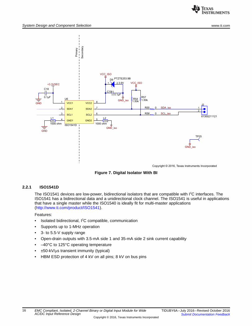
Figure 7. Digital Isolator With BI
2.2.1 ISO1541DThe ISO1541 devices are low-power, bidirectional isolators that are compatible with I2C interfaces. TheISO1541 has a bidirectional data and a unidirectional clock channel. The ISO1541 is useful in applicationsthat have a single master while the ISO1540 is ideally fit for multi-master applications(http://www.ti.com/product/ISO1541).
Features:• Isolated bidirectional, I2C compatible, communication• Supports up to 1-MHz operation• 3- to 5.5-V supply range• Open-drain outputs with 3.5-mA side 1 and 35-mA side 2 sink current capability• –40°C to 125°C operating temperature• ±50-kV/μs transient immunity (typical)• HBM ESD protection of 4 kV on all pins; 8 kV on bus pins
EMC Compliant, Isolated, 2-Channel Binary or Digital Input Module for WideAC/DC Input Reference Design
2.2.2 ISO7320CDR or ISO7320FDRThe ISO732x provides galvanic isolation up to 3000 VRMS for 1 minute per UL and 4242 VPK per VDE.These devices have two isolated channels comprised of logic input and output buffers separated by silicondioxide (SiO2) insulation barriers. The ISO7320 has two channels in the same direction. In case of inputpower or signal loss, the default output is low for devices with the suffix 'F' and high for devices without thesuffix 'F'. Used in conjunction with isolated power supplies, these devices prevent noise currents on a databus or other circuits from entering the local ground and interfering with or damaging sensitive circuitry. TheISO732x have integrated noise filters for harsh industrial environments where short noise pulses may bepresent at the device input pins. The ISO732x have TTL input thresholds and operate from 3- to 5.5-Vsupply levels (http://www.ti.com/product/ISO7320C).
Features:• Signaling rate: 25 Mbps• Integrated noise filter on the inputs• Default output high and low options• Low power consumption: Typical ICC per channel at 1 Mbps:
– ISO7320: 1.2 mA (5-V supplies), 0.9 mA (3.3-V supplies)– ISO7321: 1.7 mA (5-V supplies), 1.2 mA (3.3-V supplies)
EMC Compliant, Isolated, 2-Channel Binary or Digital Input Module for WideAC/DC Input Reference Design
2.2.3 ISO7820DWR of ISO7820FDWRThe ISO7820 is a high-performance, dual-channel digital isolator with 8000-VPK isolation voltage Theisolator provides high electromagnetic immunity and low emissions at low power consumption, whileisolating CMOS or LVCMOS digital I/Os. The ISO7820 has two forward channels and no reverse-directionchannel. If the input power or signal is lost, the default output is high for the ISO7820 and low for theISO7820F. Used in conjunction with isolated power supplies, this device prevents noise currents on a databus or other circuits from entering the local ground and interfering with or damaging sensitive circuitry(http://www.ti.com/product/iso7820/description/).
Features:• Signaling rate: Up to 100 Mbps• Wide supply range: 2.25 to 5.5 V• 2.25- to 5.5-V level translation• Wide temperature range: –55°C to 125°C• Low power consumption, Typical 1.7 mA per channel at 1 Mbps• Low propagation delay: 11 ns typical (5-V supplies)• Industry leading CMTI (Min): ±100 kV/μs• Robust EMC• System-level ESD, EFT, and Surge immunity• Low emissions• Isolation barrier life: > 25 years
Table 9. ISO7820DW Specifications
PARAMETER VALUEManufacturer part number ISO7820DW
Technology Capacitive couplingNumber of channels 2Inputs: Side 1/Side 2 2/0
Channel type UnidirectionalIsolation voltage 5700 VRMS
EMC Compliant, Isolated, 2-Channel Binary or Digital Input Module for WideAC/DC Input Reference Design
2.3 Isolated Power Supply
Figure 8. Isolated Power Supply
2.3.1 Push-Pull Driver for Isolated Power Supplies (SN6501DBV)The SN6501 is a monolithic oscillator and power-driver, specifically designed for small form factor, isolatedpower supplies in isolated interface applications. The device drives a low-profile, center-tappedtransformer primary from a 3.3-V or 5-V DC power supply. The secondary can be wound to provide anyisolated voltage based on the transformer turns ratio.
The SN6501 consists of an oscillator followed by a gate drive circuit that provides the complementaryoutput signals to drive the ground referenced N-channel power switches. The internal logic ensures breakbefore-make action between the two switches. The SN6501 is available in a small SOT-23 (5) packageand is specified for operation at temperatures from –40°C to 125°C.
Features:• Push-pull driver for small transformers• Single 3.3- or 5-V supply• High primary-side current drive:
– 5-V supply: 350 mA (max)– 3.3-V supply: 150 mA (max)
• Low ripple on rectified output permits small output capacitors• Small 5-pin SOT-23 package
EMC Compliant, Isolated, 2-Channel Binary or Digital Input Module for WideAC/DC Input Reference Design
2.3.3 Power Supply Overvoltage and ESD Protection Zener (PTZTE253.9B)
Table 11. 3.9-V Power Supply Protection Zener Diode Specification
PARAMETER SPECIFICATIONVoltage—Zener (Nom; Vz) 4.1 V
Tolerance ±6%Power—Max 1 W
Impedance (Max; Zzt) 15 Ω
Current—Reverse leakage at Vr 40 µA at 1 VMounting type Surface mount
Package or case DO-214AC, SMASupplier device package PMDS
2.3.4 LDOThe TPS70933DBVT linear regulator is an ultra-low, quiescent current device designed for powersensitive applications. A precision band-gap and error amplifier provides 2% accuracy over temperature. Aquiescent current of only 1 μA makes these devices ideal solutions for battery-powered, always-onsystems that require very little idle-state power dissipation. These devices have thermal-shutdown,current-limit, and reverse-current protections for added safety.
Table 12. 3.3-V LDO Specifications
PARAMETER SPECIFICATIONRegulator topology Positive fixedVoltage—Output 3.3 VCurrent—Output 150 mA
Voltage—Dropout (Typical) 0.96 V at 150 mANumber of regulators 1
Voltage—Input Up to 30 VCurrent—Limit (Min) 200 mA
Operating temperature –40°C to 125°CPackage SOT23-5
EMC Compliant, Isolated, 2-Channel Binary or Digital Input Module for WideAC/DC Input Reference Design
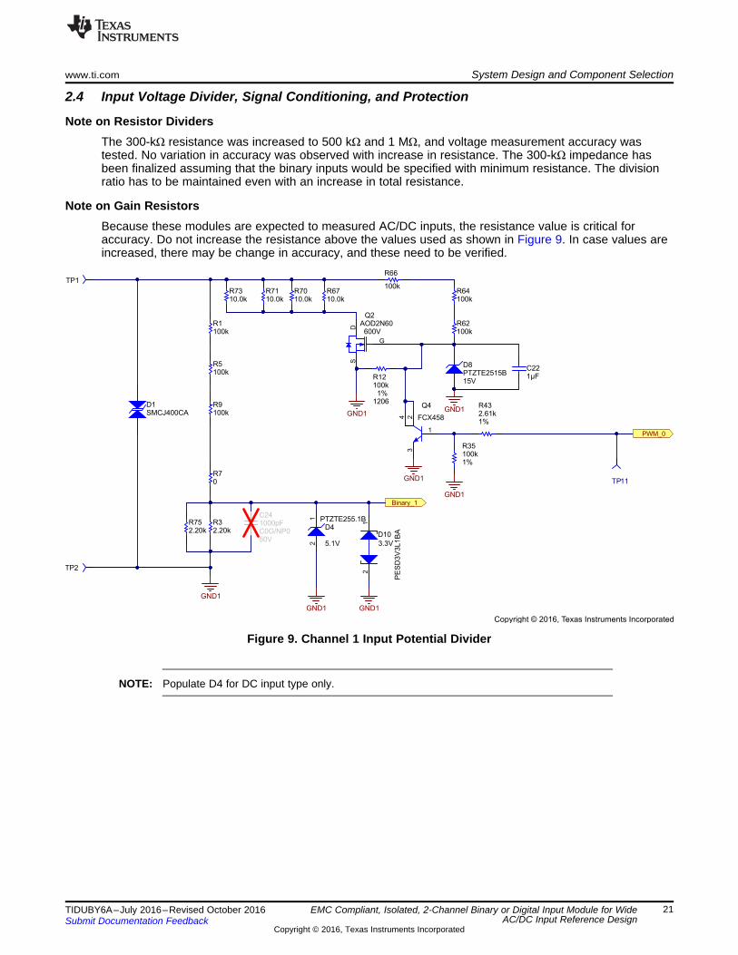
2.4 Input Voltage Divider, Signal Conditioning, and Protection
Note on Resistor DividersThe 300-kΩ resistance was increased to 500 kΩ and 1 MΩ, and voltage measurement accuracy wastested. No variation in accuracy was observed with increase in resistance. The 300-kΩ impedance hasbeen finalized assuming that the binary inputs would be specified with minimum resistance. The divisionratio has to be maintained even with an increase in total resistance.
Note on Gain ResistorsBecause these modules are expected to measured AC/DC inputs, the resistance value is critical foraccuracy. Do not increase the resistance above the values used as shown in Figure 9. In case values areincreased, there may be change in accuracy, and these need to be verified.
EMC Compliant, Isolated, 2-Channel Binary or Digital Input Module for WideAC/DC Input Reference Design
2.4.1 Input ProtectionThe binary input module is protected against overvoltage and transients. The SMCJ400CA andPESD3V3L1BA are used to achieve the required protection. These devices are optional and can be usedbased on the application.
Table 13. SMCJ400 Specifications
PARAMETER SPECIFICATIONType Zener
Bidirectional channels 1Voltage—Reverse standoff (Typ) 400 V
Voltage—Breakdown (Min) 447 VVoltage—Clamping (Max) at IPP 648 V
EMC Compliant, Isolated, 2-Channel Binary or Digital Input Module for WideAC/DC Input Reference Design
2.4.2 Resistor DividerA 100-kΩ 1206 package resistor, which can withstand a maximum voltage of 200 V, is selected for thisapplication. The
2.4.3 ADC Input Overvoltage Protection (PTZTE255.1B)A Zener diode is used to protect the electronic circuit from overvoltage and ESD.
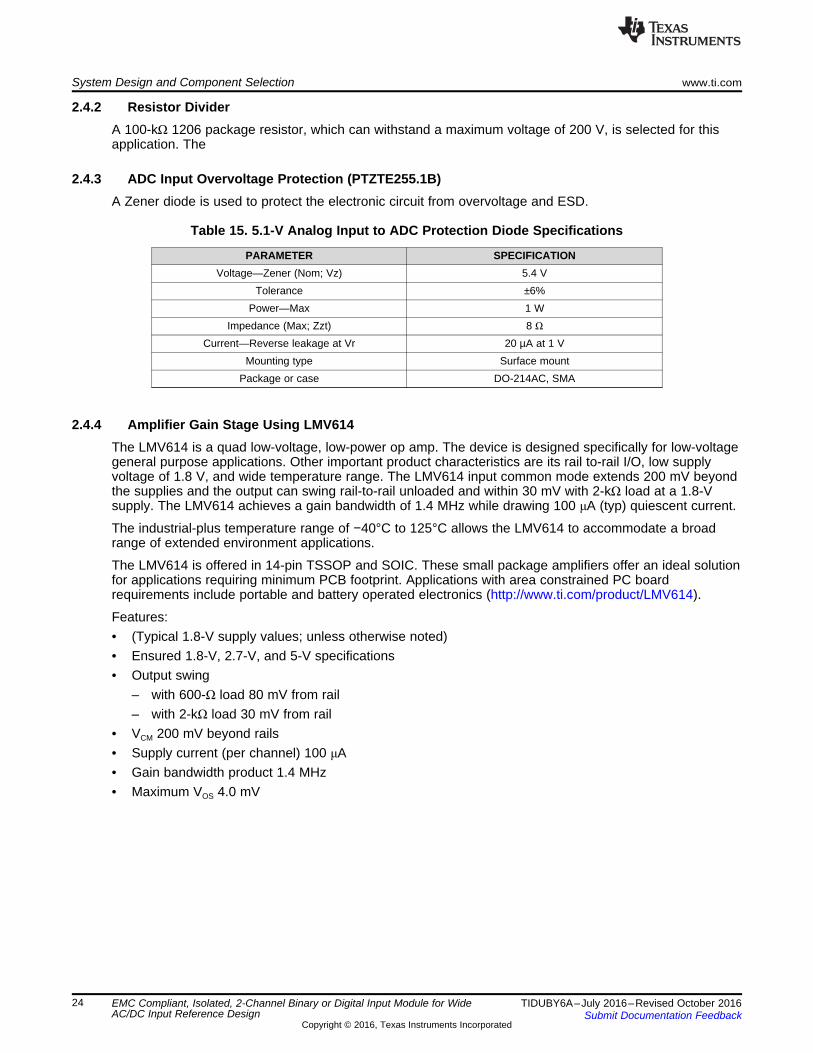
Table 15. 5.1-V Analog Input to ADC Protection Diode Specifications
PARAMETER SPECIFICATIONVoltage—Zener (Nom; Vz) 5.4 V
Tolerance ±6%Power—Max 1 W
Impedance (Max; Zzt) 8 Ω
Current—Reverse leakage at Vr 20 µA at 1 VMounting type Surface mount
Package or case DO-214AC, SMA
2.4.4 Amplifier Gain Stage Using LMV614The LMV614 is a quad low-voltage, low-power op amp. The device is designed specifically for low-voltagegeneral purpose applications. Other important product characteristics are its rail to-rail I/O, low supplyvoltage of 1.8 V, and wide temperature range. The LMV614 input common mode extends 200 mV beyondthe supplies and the output can swing rail-to-rail unloaded and within 30 mV with 2-kΩ load at a 1.8-Vsupply. The LMV614 achieves a gain bandwidth of 1.4 MHz while drawing 100 μA (typ) quiescent current.
The industrial-plus temperature range of −40°C to 125°C allows the LMV614 to accommodate a broadrange of extended environment applications.
The LMV614 is offered in 14-pin TSSOP and SOIC. These small package amplifiers offer an ideal solutionfor applications requiring minimum PCB footprint. Applications with area constrained PC boardrequirements include portable and battery operated electronics (http://www.ti.com/product/LMV614).
EMC Compliant, Isolated, 2-Channel Binary or Digital Input Module for WideAC/DC Input Reference Design
2.4.5 ReferenceThe DC reference for level-shifting is generated using the LM4041.
2.4.5.1 Adjustable Precision Shunt Voltage ReferenceThe LM4041 series of shunt voltage references are versatile, easy-to-use references suitable for a widearray of applications. The reference is used for level shifting the AC voltage input by AVDD/2. The inputvoltage is shifted to 1.65 V. This series requires no external capacitors for operation and is stable with allcapacitive loads. Additionally, the reference offers low-dynamic impedance, low noise, and a low-temperature coefficient to ensure a stable output voltage over a wide range of operating currents andtemperatures. The LM4041 uses fuse and Zener-zap reverse breakdown voltage trim during wafer sort tooffer four output voltage tolerances, ranging from 0.1% (max) for the A grade to 1% (max) for the D grade.As a result, a great deal of flexibility is offered to designers in choosing the best cost-to-performance ratiofor their applications. The LM4041 is available in a fixed (1.225 V nominal) or an adjustable version, whichrequires an external resistor divider to set the output to a value between 1.225 and 10 V.
Features:• Small packages: SOT23, SC70-5• No output capacitor required• Output voltage tolerance• LM4041D: ±1% at 25°C• Low output noise: 20 μVRMS (10 Hz to 10 kHz)• Wide operating current range: 60 μA to 12 mA• Extended temperature range: –40°C to 125°C• Low temperature coefficient: 100 ppm/°C (max)
2.4.5.2 Buffer for ReferenceThe LMV551 are high-performance, low-power op amps implemented with TI’s advanced VIP50 process.They feature 3 MHz of bandwidth while consuming only 37 μA of current per amplifier, which is anexceptional bandwidth to power ratio in this op amp class. These amplifiers are unity gain stable andprovide an excellent solution for low power applications requiring a wide bandwidth.
EMC Compliant, Isolated, 2-Channel Binary or Digital Input Module for WideAC/DC Input Reference Design
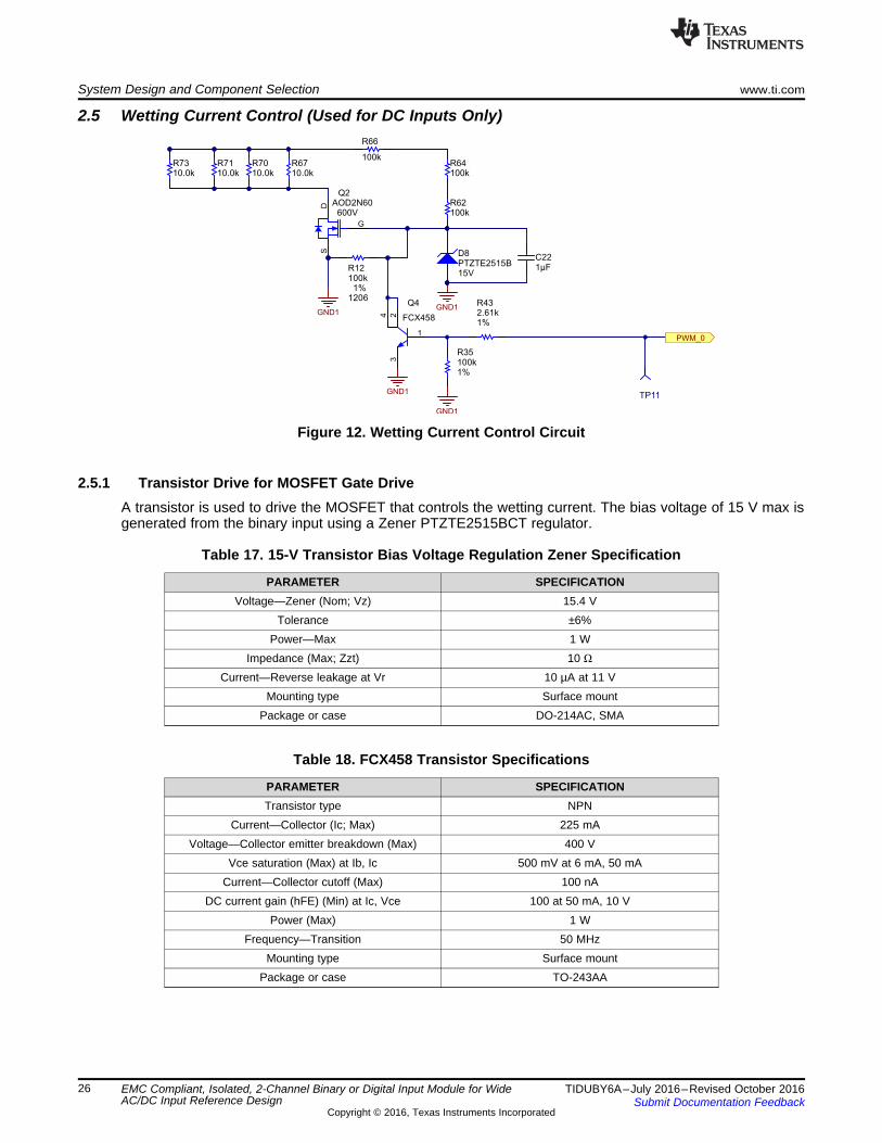
2.5 Wetting Current Control (Used for DC Inputs Only)
Figure 12. Wetting Current Control Circuit
2.5.1 Transistor Drive for MOSFET Gate DriveA transistor is used to drive the MOSFET that controls the wetting current. The bias voltage of 15 V max isgenerated from the binary input using a Zener PTZTE2515BCT regulator.
Table 17. 15-V Transistor Bias Voltage Regulation Zener Specification
PARAMETER SPECIFICATIONVoltage—Zener (Nom; Vz) 15.4 V
Tolerance ±6%Power—Max 1 W
Impedance (Max; Zzt) 10 Ω
Current—Reverse leakage at Vr 10 µA at 11 VMounting type Surface mount
Package or case DO-214AC, SMA
Table 18. FCX458 Transistor Specifications
PARAMETER SPECIFICATIONTransistor type NPN
Current—Collector (Ic; Max) 225 mAVoltage—Collector emitter breakdown (Max) 400 V
Vce saturation (Max) at Ib, Ic 500 mV at 6 mA, 50 mACurrent—Collector cutoff (Max) 100 nA
DC current gain (hFE) (Min) at Ic, Vce 100 at 50 mA, 10 VPower (Max) 1 W
Frequency—Transition 50 MHzMounting type Surface mount
EMC Compliant, Isolated, 2-Channel Binary or Digital Input Module for WideAC/DC Input Reference Design
2.5.2 Current Limiting Resistors and MOSFET (AOD2N60A)
Table 19. Wetting Current Control MOSFET Specifications
PARAMETER SPECIFICATIONFET type MOSFET N-channel, metal oxide
FET feature StandardDrain-to-source Voltage (VDS) 600 V
Current—Continuous drain (Id) at 25°C 2 A (Tc)Rds On (Max) at Id, Vgs 4.7 Ω at 1 A, 10 V
VGS(th) (Max) at Id 4.5 V at 250 µAGate charge (Qg) at Vgs 11 nC at 10 V
Input capacitance (Ciss) at VDS 295 pF at 25 VPower (Max) 57 W
Mounting type Surface mountPackage or case TO-252-3, DPak (two leads + tab), SC-63
Supplier device package TO-252 (D-Pak)
Four resistors, 1206 package 10-kΩ each in parallel, are used as current limit for wetting current. A D-PAKMOSFET with a 600-V rating is used for enhanced reliability.
2.6 Host InterfaceThe host interface can be simulated using an I2C interface. The following steps are for the binary moduleand the host interface:• The binary module is configured to be the master.• The binary module computes the required RMS value.• The measured value can be communicated to the host.
The I2C interface is available in the ISO1541D family. When using the ISO7320 or ISO7820 family ofdigital isolators, one-way communication is simulated to send out the data to the host. The bit bangingmethod can be followed with the binary module as the master generating DATA and clock.
For an alternate interface approach, the thresholds can be set using jumpers, and a digital isolator can beused as a digital output to indicate the DC input status.
2.7 Hardware Design Guidelines• Input voltage divider selection: Ensure the resistors are de-rated by 30% for the maximum withstand
The voltage rating.• Wetting current control resistor selection: The short time overload capability must be greater than 2.5
times the normal voltage withstand capability for one second.• 15-V Zener selection for MOSFET switching: Vz must be constant for wide bias currents. The Zener
current must be as low as possible to reduce power loss.• Zener selection for ADC input overvoltage protection: At lower biasing, current Vz reduces and this will
clip the input voltage affecting accuracy. The Vz at low bias current must be selected such that at thelowest input voltage, the voltage would be sufficient to bias the MOSFET.
2.8 EnhancementsA different solution is discussed in this design guide. The TI digital isolator portfolio is listed at theProducts for Digital Isolators page (http://www.ti.com/lsds/ti/isolation/digital-isolators-products.page#). TIhas roadmap of products including high-speed, robust EMC digital isolators(http://www.ti.com/product/ISO7741).
EMC Compliant, Isolated, 2-Channel Binary or Digital Input Module for WideAC/DC Input Reference Design
3 Getting Started Hardware and Software
3.1 Hardware
3.1.1 Power ConnectionThe binary input module is powered by a 3.3-V DC input from the host side. The isolated power isgenerated on board. The 3.3-V DC input is connected as shown in Table 20:
Table 20. Power Supply Connection to Binary Module
PINS SIGNAL NAMETP27 3.3 VTP28 Ground
3.1.2 Input Voltage (Digital Input) Connection
Table 21. Binary Input Connection
INPUT PINS SIGNAL NAME
BI 1TP1 DC input +veTP2 DC input –ve
BI 2TP3 DC input +veTP4 DC input –ve
3.1.3 Host Interface
Table 22. Binary Module Digital Output to HostInterface
PINS SIGNAL NAMEJ2-Pin1 Data outJ2-Pin2 Clock outTP25 Ground
EMC Compliant, Isolated, 2-Channel Binary or Digital Input Module for WideAC/DC Input Reference Design
3.2 Software
3.2.1 Initialization
Table 23. MCU Peripherals Initialization for AC/DC Binary Module Functionality
FUNCTIONALITY DESCRIPTIONMCU clock SMCLK and DCO are initialized to 1 MHz
Timer
1. Configure the timer capture control register (TA0CCTL0) to select no capture CMx as 0,compare/capture input selected as CCIxA, output mode OUTMODx as 0 and enable compare interruptCCIE.
2. Timer A programmed to provide interrupt every 200 µs (or any other sampling interval desired). Set thesampling interval (TA0CCR0)
3. Configure the Timer A control register (TA0CTL) to choose SMCLK, divider as 1 and up/down mode.
ADC – Four channels
1. Disable conversion.2. Configure the following options for the ADC control register0 (ADC10CTL0):
(a) Enable ADC interrupt.(b) Switch ON ADC.(c) Set the sample and hold time to 16× ADC10CLKs.(d) Set the reference voltages for ADC: VR+ = VCC and VR– = VSSADC10CTL0, once configured, does not need to be changed to switch between different channels.
3. Configure the following options for the ADC control register0 (ADC10CTL1):(a) Set the mode to single channel single conversion.(b) Set the ADC clock to ADC1OSC.(c) Set the divider to 1.(d) Set the sampling trigger to ADC10SC bit.(e) Set the channel to be sampled (A0).
4. Enable ADC channels ADC10AE0.5. Enable conversion.6. Once the sampling interval timer issues a trigger, the first ADC channel (A0) is sampled.
(a) Once the sample value for channel A0 is read from ADC10MEM, clear the ADC10SC bit.(b) Reinitialize ADC10CTL1 and ADC10AE0 with the other desired ADC channel (A3, A4, or A5).(c) Conversion can be started by making the ADC10SC bit high.(d) Repeat the same process for the other channels (every sampling interval) until all channels have
been sampled.
Ports 1. Configure the direction of the ports (P1DIR); 0 as inputs and 1 as outputs.2. Set the default values for outputs (0 as low, 1 as high).
I2C
1. Set the output pins for I2C (P1.6 and P1.7) to high.2. Enable the pull up resistors for P1.6 and P1.7 (P1REN).3. Enable the USI function by setting the USIPE6 and USIPE7 bits in USICTL0 register.4. Disable the USI peripheral using software reset (USISWRST bit).5. Enable I2C mode and USI interrupt enable.6. Set clock polarity.7. Disable automatic clear control (USIIFGCC bit).8. Enable USI peripheral by clearing the (USISWRST bit).
1. Stop the watchdog timer.2. Initialize the clocks to set SMCLK to 1 MHz.3. Disable all interrupts.4. Set the direction of port pins to default values.5. Initialize I2C in master mode6. Configure Timer A to provide an interval based interrupt using compare register. The timer interrupt can
be used to periodically trigger ADC sampling.7. Initialize ADC to sample one ADC channel. Re-initialize ADC10CTL1 and ADC10AE0 to sample a
different ADC channel.8. Enable all interrupts.
ADC samplecapturing for all four
channels
• Samples are triggered by setting ADC10SC bit. (From the timer interrupt for the first channel, meaningA0).
• When conversion is complete, it triggers an interrupt. The result is obtained by reading the registerADC10MEM.
• Reinitialize the ADC to read the other ADC channels and issue ADC10SC trigger. Repeat this step toread the other ADC channels.
ADC samplesintegration
• After the value is read from ADC10MEM, the offset has to be corrected.• For each ADC channel, the sample values are added over a timer period (1 ms) and then averaged by
dividing with the number of sample counts.
30- and 60-ms ADCcount calculation
Calculation of 1-ms average (for each channel):• The 1-ms average for each channel can be stored for three iterations (that is, three such 1-ms average
values).Calculation of 3-ms average (for each channel):
• 3-ms average can be calculated using the three counts of 1-ms averages and is stored for 10 or 20counts.
Calculation of 30- or 60-ms average (for each channel):• 10 or 20 counts of 3-ms average is stored and can be averaged to provide 30 or 60 ms average.
I2C interface forcommunicating ADC
count to host
• The 30-ms average values for all four channels can be transmitted over I2C to the host processor.• A pre-requisite for this is to have a host processor (for example, LaunchPad) that runs as an I2C slave.• The master sends 30-ms averages for each channel on I2C.
EMC Compliant, Isolated, 2-Channel Binary or Digital Input Module for WideAC/DC Input Reference Design
Table 29. Converting ADC Count to Voltage — AC Input Low Gain
PARAMETER SPECIFICATIONADCref — peak 1.65 VMaximum input 315 V
Gain factor 1Max ADC count for RMS input 512 / 1.414 = 362
RMS voltage equivalent for one ADC count Maximum input / (ADC count × Gain factor) = 0.870
The minimum ADC resolution of 1 count equals approximately 1 V. To overcome this issue, a gain stageof 3.4 is used.
Table 30. Converting ADC Count to Voltage — AC Input High Gain
PARAMETER SPECIFICATIONADCref — peak 1.65 VMaximum input 315 V
Gain factor 3.4Max ADC count for RMS input 512 / 1.414 = 362
RMS voltage equivalent for one ADC count Maximum input / (ADC count × Gain factor) = 0.260
3.2.4 Programming
Figure 13. Spy-Bi-Wire Basic Concept
The 2-wire interface is made up of the SBWTCK (Spy-Bi-Wire test clock) and SBWTDIO (Spy-Bi-Wire testdata I/O) pins. The SBWTCK signal is the clock signal and is a dedicated pin. In normal operation, this pinis internally pulled to ground. The SBWTDIO signal represents the data and is a bidirectional connection.To reduce the overhead of the 2-wire interface, the SBWTDIO line is shared with the RST/NMI pin of thedevice.
EMC Compliant, Isolated, 2-Channel Binary or Digital Input Module for WideAC/DC Input Reference Design
4 Testing and Results
4.1 Test Setup
Figure 14. Test Setup for Binary Module Performance
The test setup for testing the binary module consists of• DC power supply (3.3 V)• AC or DC input voltage (20 to 270 V)• TIDA-00809 board with BI or RI digital isolators• GUI for firmware upgrade and data capture
Ensure the inputs do not exceed the range specified above for proper operation.
4.2 Test Data
4.2.1 Functional Testing
Table 31. Functional Testing
PARAMETER SPECIFICATION MEASUREMENTIsolated supply 3.3 V 3.31
Reference output 1.65 V 1.645Op amp gain ×1 , ×3.7 OK
MCU programming Spy-Bi-Wire OK
4.2.2 Voltage Measurement Accuracy Testing
NOTE: The readings in the following subsections are measurements taken without any calibration.The errors include component tolerances and ADC errors. The accuracy can be improved byintroducing software calibration.
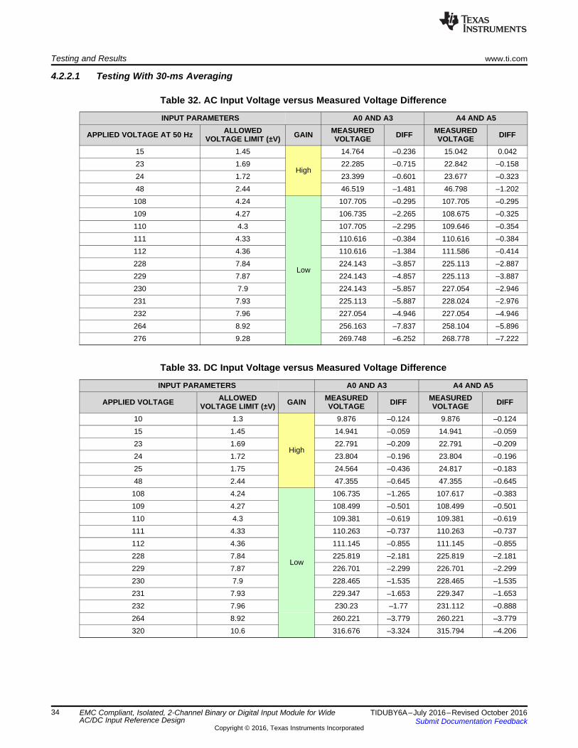
The errors observed can be further improved by calibrating gain. To ensure that the results are less than±3.0% of the ±1-V measured value (programmable step size), applying gain calibration is recommended.The gain calibration can be applied on the host side or binary module side. For initial testing, averagingwas done for 10, 30, and 60 ms. The measurement was repeatable at 30 and 60 ms for AC input, andthere was no difference observed in the measured values. In case measurements are expected to bedone faster than 30 ms, characterize accuracy before implementing.
EMC Compliant, Isolated, 2-Channel Binary or Digital Input Module for WideAC/DC Input Reference Design
4.2.2.4 Wetting Current Measurement
Table 37. Wetting Current Measurement at Different Voltage Inputs (DC Only)
DC VOLTAGE INPUT SWITCHED ONFOR 50 ms IMPEDANCE INPUT 1
CURRENT (mA) DUTY CYCLE INPUT 2CURRENT (mA) DUTY CYCLE
24 V 2.5 K ~9 N/A ~9 N/A110 V 2.5 K ~44 N/A ~44 N/A230 V 2.5 K ~44 50% ~44 50%
4.2.2.5 Drift Due to Temperature Variation of Signal Conditioning CircuitThe signal conditioning circuit consisting of the resistor divider, the 400-V input TVS, 5.1-V ADC inputprotection Zener, was tested for temperature variation. The leakage current for the 400-V TVS is < 1 µA atrated voltage for SMCJ package. The following results indicate that the effect of leakage current does notsignificantly influence the voltage input to ADC.
Table 38. Voltage Drift With Temperature at 300-V Input
TEMPERATURE (°C) MEASURED VOLTAGE (V) DIFFERENCE (–V)–10 298.92 –1.08212 299.01 –0.98640 299.01 –0.98670 299.11 –0.890
Table 39. Voltage Drift With Temperature at 110-V Input
TEMPERATURE (°C) MEASURED VOLTAGE (V) DIFFERENCE (–V)–10 109.84 –0.16010 109.74 –0.25640 109.84 –0.16070 109.84 –0.160
Table 40. Voltage Drift With Temperature at 24-V Input
TEMPERATURE (°C) MEASURED VOLTAGE (V) DIFFERENCE (–V)–10 23.98 –0.01810 23.89 –0.11340 23.98 –0.01870 23.98 –0.018
EMC Compliant, Isolated, 2-Channel Binary or Digital Input Module for WideAC/DC Input Reference Design
4.2.2.6 Binary Input Testing With Digital Output (ISO7320)The binary module uses an I2C isolator to communicate the voltage reading to the host MCU.Alternatively, digital isolator can be used with the module to sense fixed voltages.
Table 41. Test Results for ISO7320
DC INPUT VIN APPLIED VOLTAGE TOLERANCE BINARY INPUT 1OBSERVATION
BINARY INPUT 2OBSERVATION
24 22 ±3% of VIN ±1 V Low Low24 26 ±3% of VIN ±1 V High High110 106 ±3% of VIN ±1 V Low Low110 114 ±3% of VIN ±1 V High High240 230 ±3% of VIN ±1 V Low Low240 250 ±3% of VIN ±1 V High High
4.2.2.7 Binary Input Testing With Digital Output (ISO7820)The digital isolator can be used with the module to sense fixed voltages.
Table 42. Test Results for ISO7820
DC INPUT VIN APPLIED VOLTAGE TOLERANCE BINARY INPUT 1OBSERVATION
BINARY INPUT 2OBSERVATION
24 22 ±3% of VIN ±1 V Low Low24 26 ±3% of VIN ±1 V High High110 106 ±3% of VIN ±1 V Low Low110 114 ±3% of VIN ±1 V High High240 230 ±3% of VIN ±1 V Low Low240 250 ±3% of VIN ±1 V High High
4.2.3 IEC Pre-Compliance Testing—Digital Isolator ISO1541D With BIThe following EMC tests have been performed.
Table 43. EMC Tests
TEST STANDARDESD IEC61000-4-2EFT IEC61000-4-4
Surge IEC61000-4-5
Table 44. Performance Criteria
CRITERIA ACCEPTANCE (PASS) CRITERIA
A The binary input module must continue to operate as intended. No loss of function or performance occur evenduring the test.
BTemporary degradation of performance is accepted.After the test, the binary input module must continue to operate as intended without manual intervention.
CDuring the test, a loss of functions accepted, but no destruction of hardware or software.After the test, the binary input module must continue to operate as intended automatically after manual restartor power off/power on.
EMC Compliant, Isolated, 2-Channel Binary or Digital Input Module for WideAC/DC Input Reference Design
4.2.3.1 IEC61000-4-2 ESD TestThe IEC610004-2 ESD test simulates the electrostatic discharge of an operator directly onto an adjacentelectronic component. An electrostatic charge usually develops in low relative humidity, and on low-conductivity carpets, or vinyl garments. To simulate a discharge event, an ESD generator applies ESDpulses to the binary input module, which can happen through direct contact with the binary input module(contact discharge), or through an air-gap (air-discharge). This was applied across signal inputs only. Aseries of 10 negative and positive pulses were applied directly on the binary inputs during the test (contactdischarge). After the test, the binary input module module was verified for functionality. The test resultsshow the binary input module was able to withstand the required discharge. The binary input module wasnot permanently damaged.
Table 45. ESD Test Steps
TEST NO TEST MODE OBSERVATION1 Contact 2 kV Pass2 Contact –2 kV Pass3 Contact 4 kV Pass4 Contact –4 kV Pass5 Contact 5 kV Pass6 Contact –5 kV Pass
Table 46. ESD Test Observations
IMMUNITY TEST STANDARD PORT TARGET VOLTAGE RESULT
ESD IEC 61000-4-2, contact Binary input ±4 kV
Pass , Criteria B(After the test, themodule continued tooperate as intended)
Figure 17. ESD Setup for Binary Input Module With BI Digital Isolator
NOTE: The ISO1541 can be used with ESD requirements up to 4 kV although these tests confirmthat the device performs without failure for a higher ESD level.
EMC Compliant, Isolated, 2-Channel Binary or Digital Input Module for WideAC/DC Input Reference Design
4.2.3.2 IEC61000-4-4 EFT TestThe burst signal is injected on the voltage inputs. The test is carried out with the binary input moduleplaced 10 cm above the reference plate. After the test, the binary input module was verified forfunctionality. The test results show the binary input module was able to withstand up to ±2 kV. The binaryinput module was able to perform normally after each test. Because functionality could not be verifiedduring the test, the result was noted as passing Class B.
The EFT burst at I/O connectors and the performance criteria expected are as follows:
EMC Compliant, Isolated, 2-Channel Binary or Digital Input Module for WideAC/DC Input Reference Design
4.2.3.3 IEC61000-4-5 Surge TestThe IEC61000-4-5 surge test simulates switching transients caused by lightning strikes or the switching ofpower systems including load changes and short circuits. The test requires five positive and five negativesurge pulses with a time interval between successive pulses of 1 minute or less. The unshieldedsymmetrical data line setup as defined by the IEC61000-4-5 specification was used for this test. The testgenerator was configured for 1.2/50-μs surges and diode clamps were used for line-to-ground coupling. Aseries of five negative and positive pulses, with 10 seconds spacing between each pulse, were appliedduring the test.
After the test, the binary module was verified for functionality. The test results show the binary inputmodule was able to withstand up to ±4 kV surge. The binary input module was able to perform normallyafter each test. Because functionality could not be verified during the test, the result was noted as passingwith Class B.
EMC Compliant, Isolated, 2-Channel Binary or Digital Input Module for WideAC/DC Input Reference Design
4.2.4 IEC Pre-Compliance Testing—Digital Isolator ISO7320 With BIThe following tests were done for the ISO7320C and ISO7320FC devices.
4.2.4.1 IEC61000-4-2 ESD TestThe IEC610004-2 ESD test simulates the electrostatic discharge of an operator directly onto an adjacentelectronic component. An electrostatic charge usually develops in low relative humidity, and on low-conductivity carpets, or vinyl garments. To simulate a discharge event, an ESD generator applies ESDpulses to the binary input module, which can happen through direct contact with the binary input module(contact discharge), or through an air-gap (air-discharge). This was applied across signal inputs only. Aseries of 10 negative and positive pulses were applied directly on the binary inputs during the test (contactdischarge). After the test, the binary module was verified for functionality. The test results show the binaryinput module was able to withstand the required discharge. The binary input module was not permanentlydamaged.
ESD IEC 61000-4-2, contact Binary input ±4 kVPass, Criteria B(After the test, the module continued tooperate as intended.)
NOTE: The ISO7320 can be used with ESD requirements up to 6 kV although these tests confirmthat the device performs without failure for a higher ESD level.
EMC Compliant, Isolated, 2-Channel Binary or Digital Input Module for WideAC/DC Input Reference Design
4.2.4.2 IEC61000-4-4 EFT TestThe burst signal is injected on the voltage inputs. The test is carried out with the binary input moduleplaced 10 cm above the reference plate. After the test, the binary module was verified for functionality.The test results show the binary input module was able to withstand up to ±2 kV. The binary input modulewas able to perform normally after each test. Because functionality could not be verified during the test,the result was noted as passing Class B.
The EFT burst at I/O connectors and the performance criteria expected are as follows:
4.2.4.3 IEC61000-4-5 Surge TestThe IEC61000-4-5 surge test simulates switching transients caused by lightning strikes or the switching ofpower systems including load changes and short circuits. The test requires five positive and five negativesurge pulses with a time interval between successive pulses of 1 minute or less. The unshieldedsymmetrical data line setup as defined by the IEC61000-4-5 specification was used for this test. The testgenerator was configured for 1.2/50-μs surges and diode clamps were used for line-to-ground coupling. Aseries of five negative and positive pulses, with 10 seconds spacing between each pulse, were appliedduring the test.
After the test, the binary module was verified for functionality. The test results show the binary inputmodule was able to withstand up to ±4 kV surge. The binary input module was able to perform normallyafter each test. Because functionality could not be verified during the test, the result was noted as passingwith Class B.
Table 55. Surge Test Observations
IMMUNITY TEST STANDARD PORT TARGET VOLTAGE RESULT
Surge, DMIEC 61000-4-5: (1.2/50μs to 8/20 μs), 42 Ω–0.5μF
Binary input signal line ± 4 kV
Pass, Criteria B(After the test, themodule continued tooperate as intended.)
Table 56. Surge Test Steps
TEST NO TEST MODE OBSERVATION1 1.0 kV Pass2 –1.0 kV Pass3 2.0 kV Pass4 –2.0 kV Pass5 4.0 kV Pass
EMC Compliant, Isolated, 2-Channel Binary or Digital Input Module for WideAC/DC Input Reference Design
Table 56. Surge Test Steps (continued)TEST NO TEST MODE OBSERVATION
6 –4.0 kV Pass
4.2.5 IEC Pre-Compliance Testing—Digital Isolator ISO7820 With RIThe following tests were done for the ISO7520CDW, ISO7820, and ISO7820F devices.
4.2.5.1 IEC61000-4-2 ESD TestThe IEC610004-2 ESD test simulates the electrostatic discharge of an operator directly onto an adjacentelectronic component. An electrostatic charge usually develops in low relative humidity, and on low-conductivity carpets, or vinyl garments. To simulate a discharge event, an ESD generator applies ESDpulses to the binary input module, which can happen through direct contact with the binary input module(contact discharge), or through an air-gap (air-discharge). This was applied across signal inputs only. Aseries of 10 negative and positive pulses were applied directly on the binary inputs during the test (contactdischarge). After the test, the binary module was verified for functionality. The test results show the binaryinput module was able to withstand the required discharge. The binary input module was not permanentlydamaged.
Table 57. ESD Test Steps
TEST NO TEST MODE OBSERVATION1 Contact 2 kV Pass2 Contact –2 kV Pass3 Contact 4 kV Pass4 Contact –4 kV Pass5 Contact 8 kV Pass6 Contact –8 kV Pass
Table 58. ESD Test Observations
IMMUNITY TEST STANDARD PORT TARGET VOLTAGE RESULT
ESD IEC 61000-4-2, contact Signal lines ±8 kV
Pass, Criteria B(After the test, themodule continued tooperate as intended.)
Figure 20. ESD Setup for Binary Input Module With RI
The burst signal is injected on the voltage inputs. The test is carried out with the binary input moduleplaced 10 cm above the reference plate. After the test, the binary module was verified for functionality.The test results show the binary input module was able to withstand up to ±2 kV. The binary input modulewas able to perform normally after each test. Because functionality could not be verified during the test,the result was noted as passing Class B.
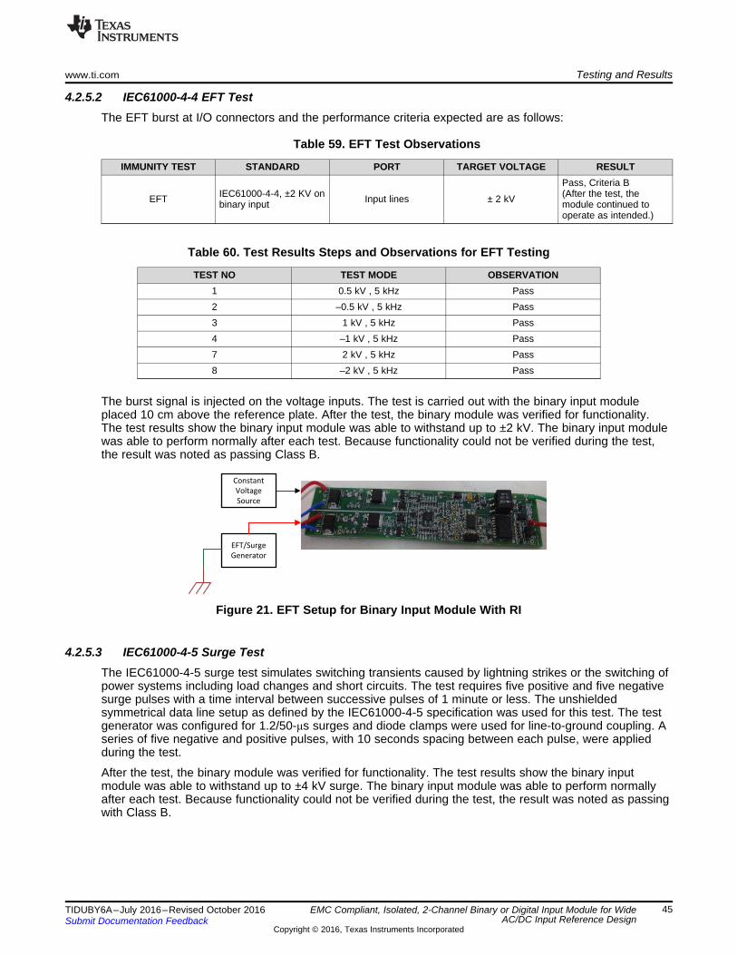
Figure 21. EFT Setup for Binary Input Module With RI
4.2.5.3 IEC61000-4-5 Surge TestThe IEC61000-4-5 surge test simulates switching transients caused by lightning strikes or the switching ofpower systems including load changes and short circuits. The test requires five positive and five negativesurge pulses with a time interval between successive pulses of 1 minute or less. The unshieldedsymmetrical data line setup as defined by the IEC61000-4-5 specification was used for this test. The testgenerator was configured for 1.2/50-μs surges and diode clamps were used for line-to-ground coupling. Aseries of five negative and positive pulses, with 10 seconds spacing between each pulse, were appliedduring the test.
After the test, the binary module was verified for functionality. The test results show the binary inputmodule was able to withstand up to ±4 kV surge. The binary input module was able to perform normallyafter each test. Because functionality could not be verified during the test, the result was noted as passingwith Class B.
Pass, Criteria B(After the test, themodule continued tooperate as intended.)
Table 62. Surge Test Steps
TEST NO TEST MODE OBSERVATION1 1.0 kV Pass2 –1.0 kV Pass3 2.0 kV Pass4 –2.0 kV Pass5 4.0 kV Pass6 –4.0 kV Pass
Figure 22. Surge Setup for Binary Input Module With RI
4.2.6 Summary
Table 63. Test Results Summary for AC/DC Binary Input Module—BI and RI
TEST OBSERVATIONPower supply: Binary module with BI and RI OKMeasurement of AC/DC voltage input with BI and RI digital isolators OKAC/DC input voltage measurement accuracy < ±3% ± 1 VEMC pre-compliance (ESD, EFT, Surge) testing for the binary input module with BI OKEMC pre-compliance (ESD, EFT, Surge) testing for the binary input module with RI OK
8 About the AuthorKALLIKUPPA MUNIYAPPA SREENIVASA is a systems architect at Texas Instruments where he isresponsible for developing reference design solutions for the industrial segment. Sreenivasa brings to thisrole his experience in high-speed digital and analog systems design. Sreenivasa earned his bachelor ofelectronics (BE) in electronics and communication engineering (BE-E&C) from VTU, Mysore, India.
Revision A HistoryNOTE: Page numbers for previous revisions may differ from page numbers in the current version.
Changes from Original (July 2016) to A Revision ........................................................................................................... Page
• Changed from preview page............................................................................................................. 1• Changed title from EMC Compliant, Group Isolated, 2-Channel Binary Input Module for Wide AC/DC Input Reference
Design ...................................................................................................................................... 1• Deleted "Measurement Resolution Better Than 1 V" from Features ............................................................... 1• Added "PLC Digital Input Module" to Applications .................................................................................... 1• Changed measurement resolution range limit from 270-V AC/DC to 264-V AC/DC ............................................. 7• Changed electrical isolation level from >2 kVRMS to 5700 VRMS ...................................................................... 7• Added note under Figure 9 ............................................................................................................. 21• Added note under Figure 10 ........................................................................................................... 22• Changed target voltage in ESD test from ±8 kV to ±4 kV .......................................................................... 39• Changed target voltage in ESD test from ±8 kV to ±6 kV .......................................................................... 42
Texas Instruments Incorporated (‘TI”) reference designs are solely intended to assist designers (“Designer(s)”) who are developing systemsthat incorporate TI products. TI has not conducted any testing other than that specifically described in the published documentation for aparticular reference design.TI’s provision of reference designs and any other technical, applications or design advice, quality characterization, reliability data or otherinformation or services does not expand or otherwise alter TI’s applicable published warranties or warranty disclaimers for TI products, andno additional obligations or liabilities arise from TI providing such reference designs or other items.TI reserves the right to make corrections, enhancements, improvements and other changes to its reference designs and other items.Designer understands and agrees that Designer remains responsible for using its independent analysis, evaluation and judgment indesigning Designer’s systems and products, and has full and exclusive responsibility to assure the safety of its products and compliance ofits products (and of all TI products used in or for such Designer’s products) with all applicable regulations, laws and other applicablerequirements. Designer represents that, with respect to its applications, it has all the necessary expertise to create and implementsafeguards that (1) anticipate dangerous consequences of failures, (2) monitor failures and their consequences, and (3) lessen thelikelihood of failures that might cause harm and take appropriate actions. Designer agrees that prior to using or distributing any systemsthat include TI products, Designer will thoroughly test such systems and the functionality of such TI products as used in such systems.Designer may not use any TI products in life-critical medical equipment unless authorized officers of the parties have executed a specialcontract specifically governing such use. Life-critical medical equipment is medical equipment where failure of such equipment would causeserious bodily injury or death (e.g., life support, pacemakers, defibrillators, heart pumps, neurostimulators, and implantables). Suchequipment includes, without limitation, all medical devices identified by the U.S. Food and Drug Administration as Class III devices andequivalent classifications outside the U.S.Designers are authorized to use, copy and modify any individual TI reference design only in connection with the development of endproducts that include the TI product(s) identified in that reference design. HOWEVER, NO OTHER LICENSE, EXPRESS OR IMPLIED, BYESTOPPEL OR OTHERWISE TO ANY OTHER TI INTELLECTUAL PROPERTY RIGHT, AND NO LICENSE TO ANY TECHNOLOGY ORINTELLECTUAL PROPERTY RIGHT OF TI OR ANY THIRD PARTY IS GRANTED HEREIN, including but not limited to any patent right,copyright, mask work right, or other intellectual property right relating to any combination, machine, or process in which TI products orservices are used. Information published by TI regarding third-party products or services does not constitute a license to use such productsor services, or a warranty or endorsement thereof. Use of the reference design or other items described above may require a license from athird party under the patents or other intellectual property of the third party, or a license from TI under the patents or other intellectualproperty of TI.TI REFERENCE DESIGNS AND OTHER ITEMS DESCRIBED ABOVE ARE PROVIDED “AS IS” AND WITH ALL FAULTS. TI DISCLAIMSALL OTHER WARRANTIES OR REPRESENTATIONS, EXPRESS OR IMPLIED, REGARDING THE REFERENCE DESIGNS OR USE OFTHE REFERENCE DESIGNS, INCLUDING BUT NOT LIMITED TO ACCURACY OR COMPLETENESS, TITLE, ANY EPIDEMIC FAILUREWARRANTY AND ANY IMPLIED WARRANTIES OF MERCHANTABILITY, FITNESS FOR A PARTICULAR PURPOSE, AND NON-INFRINGEMENT OF ANY THIRD PARTY INTELLECTUAL PROPERTY RIGHTS.TI SHALL NOT BE LIABLE FOR AND SHALL NOT DEFEND OR INDEMNIFY DESIGNERS AGAINST ANY CLAIM, INCLUDING BUT NOTLIMITED TO ANY INFRINGEMENT CLAIM THAT RELATES TO OR IS BASED ON ANY COMBINATION OF PRODUCTS ASDESCRIBED IN A TI REFERENCE DESIGN OR OTHERWISE. IN NO EVENT SHALL TI BE LIABLE FOR ANY ACTUAL, DIRECT,SPECIAL, COLLATERAL, INDIRECT, PUNITIVE, INCIDENTAL, CONSEQUENTIAL OR EXEMPLARY DAMAGES IN CONNECTION WITHOR ARISING OUT OF THE REFERENCE DESIGNS OR USE OF THE REFERENCE DESIGNS, AND REGARDLESS OF WHETHER TIHAS BEEN ADVISED OF THE POSSIBILITY OF SUCH DAMAGES.TI’s standard terms of sale for semiconductor products (http://www.ti.com/sc/docs/stdterms.htm) apply to the sale of packaged integratedcircuit products. Additional terms may apply to the use or sale of other types of TI products and services.Designer will fully indemnify TI and its representatives against any damages, costs, losses, and/or liabilities arising out of Designer’s non-compliance with the terms and provisions of this Notice.IMPORTANT NOTICE