3 Emerging Technology-Based Design of Primitives for Hardware Security YU BI, KAVEH SHAMSI, and JIANN-SHIUN YUAN, University of Central Florida PIERRE-EMMANUEL GAILLARDON and GIOVANNI DE MICHELI, ’Ecole Polytechnique F´ ed´ erale de Lausanne (EPFL), Switzerland XUNZHAO YIN, X. SHARON HU, and MICHAEL NIEMIER, University of Notre Dame YIER JIN, University of Central Florida Hardware security concerns such as intellectual property (IP) piracy and hardware Trojans have triggered research into circuit protection and malicious logic detection from various design perspectives. In this ar- ticle, emerging technologies are investigated by leveraging their unique properties for applications in the hardware security domain. Security, for the first time, will be treated as one design metric for emerg- ing nano-architecture. Five example circuit structures including camouflaging gates, polymorphic gates, current/voltage-based circuit protectors, and current-based XOR logic are designed to show the high effi- ciency of silicon nanowire FETs and graphene SymFET in applications such as circuit protection and IP piracy prevention. Simulation results indicate that highly efficient and secure circuit structures can be achieved via the use of non-CMOS devices. Categories and Subject Descriptors: C.2.2 [Security and Protection]: Physical Security General Terms: Security, Design Additional Key Words and Phrases: Emerging technology, hardware security, SiNW FET, graphene SymFET ACM Reference Format: Yu Bi, Kaveh Shamsi, Jiann-Shiun Yuan, Pierre-Emmanuel Gaillardon, Giovanni De Micheli, Xunzhao Yin, X. Sharon Hu, Michael Niemier, and Yier Jin. 2016. Emerging technology-based design of primitives for hardware security. J. Emerg. Technol. Comput. Syst. 13, 1, Article 3 (April 2016), 19 pages. DOI: http://dx.doi.org/10.1145/2816818 1. INTRODUCTION The emergence of hardware Trojans has largely reshaped the traditional view that the hardware layer can be blindly trusted. Hardware Trojans, which are often in the form of maliciously inserted circuitry, may impact the original design by data leakage or circuit M. Niemier and X. S. Hu were supported in part by the Center for Low Energy Systems Technology (LEAST), one of six centers of STARnet, a Semiconductor Research Corporation program sponsored by MARCO and DARPA. A preliminary version of parts of this work was published in the 23rd Asia Test Symposium (ATS) in November 2014 under the title “Leveraging Emerging Technology for Hardware Security—Case Study on Silicon Nanowire FETs and Graphene SymFETs.” Authors’ addresses: Y. Bi, K. Shamsi, J.-S. Yuan, and Y. Jin, Department of Electrical Engineering and Com- puter Science, University of Central Florida; emails: [email protected], [email protected], jiann- [email protected], [email protected]; P.-E. Gaillardon and G. de Micheli, ´ Ecole Polytechnique F´ ed´ erale de Lausanne (EPFL), Switzerland; emails: [email protected], giovanni.demicheli@ epfl.ch; X. Yin, X. S. Hu, and M. Niemier, Department of Computer Science and Engineering, University of Notre Dame; emails: {xyin1, shu, mniemier}@nd.edu. Permission to make digital or hard copies of part or all of this work for personal or classroom use is granted without fee provided that copies are not made or distributed for profit or commercial advantage and that copies show this notice on the first page or initial screen of a display along with the full citation. Copyrights for components of this work owned by others than ACM must be honored. Abstracting with credit is permitted. To copy otherwise, to republish, to post on servers, to redistribute to lists, or to use any component of this work in other works requires prior specific permission and/or a fee. Permissions may be requested from Publications Dept., ACM, Inc., 2 Penn Plaza, Suite 701, New York, NY 10121-0701 USA, fax +1 (212) 869-0481, or [email protected]. c 2016 ACM 1550-4832/2016/04-ART3 $15.00 DOI: http://dx.doi.org/10.1145/2816818 ACM Journal on Emerging Technologies in Computing Systems, Vol. 13, No. 1, Article 3, Publication date: April 2016.
Transcript
3
Emerging Technology-Based Design of Primitivesfor Hardware Security
YU BI, KAVEH SHAMSI, and JIANN-SHIUN YUAN, University of Central FloridaPIERRE-EMMANUEL GAILLARDON and GIOVANNI DE MICHELI, ’Ecole PolytechniqueFederale de Lausanne (EPFL), SwitzerlandXUNZHAO YIN, X. SHARON HU, and MICHAEL NIEMIER, University of Notre DameYIER JIN, University of Central Florida
Hardware security concerns such as intellectual property (IP) piracy and hardware Trojans have triggeredresearch into circuit protection and malicious logic detection from various design perspectives. In this ar-ticle, emerging technologies are investigated by leveraging their unique properties for applications in thehardware security domain. Security, for the first time, will be treated as one design metric for emerg-ing nano-architecture. Five example circuit structures including camouflaging gates, polymorphic gates,current/voltage-based circuit protectors, and current-based XOR logic are designed to show the high effi-ciency of silicon nanowire FETs and graphene SymFET in applications such as circuit protection and IPpiracy prevention. Simulation results indicate that highly efficient and secure circuit structures can beachieved via the use of non-CMOS devices.
Categories and Subject Descriptors: C.2.2 [Security and Protection]: Physical Security
General Terms: Security, Design
Additional Key Words and Phrases: Emerging technology, hardware security, SiNW FET, graphene SymFET
ACM Reference Format:Yu Bi, Kaveh Shamsi, Jiann-Shiun Yuan, Pierre-Emmanuel Gaillardon, Giovanni De Micheli, Xunzhao Yin,X. Sharon Hu, Michael Niemier, and Yier Jin. 2016. Emerging technology-based design of primitives forhardware security. J. Emerg. Technol. Comput. Syst. 13, 1, Article 3 (April 2016), 19 pages.DOI: http://dx.doi.org/10.1145/2816818
1. INTRODUCTION
The emergence of hardware Trojans has largely reshaped the traditional view that thehardware layer can be blindly trusted. Hardware Trojans, which are often in the form ofmaliciously inserted circuitry, may impact the original design by data leakage or circuit
malfunction. Hardware counterfeiting and intellectual property (IP) piracy are anothertwo serious issues costing the U.S. economy more than $200 billion annually [FrontierEconomics 2011]. To address such threats, various hardware Trojan detection methodsand hardware metering methods have been developed [Agrawal et al. 2007; Alkabaniand Koushanfar 2007; Jin and Makris 2008; Potkonjak et al. 2009; Jin et al. 2013].Besides circuit-level security solutions, cybersecurity researchers also rely on layeredsecurity protection approaches and have developed various methods to protect thehigher abstraction layer through security enhancement at the lower abstraction layer.Through this chain, cybersecurity protection schemes have been pushed downwardfrom virtual machine to hypervisor [Seshadri et al. 2007]. Following this trend, newmethods are under development through which the hardware infrastructure is modifiedto directly support sophisticated security policies so that a system-level protectionscheme will be more efficient [Jin and Oliveira 2014].
It is a rather common practice to think of dedicated hardware primitives that sup-port the various security applications in the multiple layers of the system hierarchy.Physical unclonable functions (PUFs) to produce unique IDs, power regulators to hinderpower analysis attacks, or encryption hardware accelerators are examples of these spe-cial types of hardware that only find applications in the security context. A large amountof research and experimentation has been carried out on the design of these primitivesbased on the currently prevailing CMOS technology. However, the security provided bythese primitives comes at the cost of large overheads mostly in terms of area.
The development of emerging technologies provides hardware security researcherswith opportunities to utilize some of the otherwise unusable properties of emergingtechnologies in security applications. Originally developed as alternatives to CMOStechnology to overcome the scaling limit, emerging technologies also demonstratedtheir unique features, which, besides improving circuit performance, can simplify cir-cuit structure for security purposes such as IP protection and Trojan detection [Biet al. 2014]. Traditional metrics, such as power and delay, are the major criteria usedto evaluate the merits of emerging devices; however, in this work, we will include thesecurity consideration in the overall performance measurements to fully compare theemerging devices to CMOS technology. Considering the large amount of emerging de-vice models, including graphene transistors, atomic switches, memristors, Mott FET,spin FET, nanomagnetic, and all-spin logic, spin wave devices, OST-RAM, magnetore-sistive random-access memory (MRAM), spintronic devices, and so forth [ITRS 2013],two fundamental questions have recently been raised related to their applications inthe hardware security domain. First, can emerging technology provide a more efficienthardware infrastructure than CMOS technology in countering hardware Trojans andIP piracy? Second, what properties should the emerging technology-based hardware in-frastructure provide so that software-level protection schemes can be better supported?
Most work with emerging technologies for security purposes to date has exploredimplementations like PUFs [Iyengar et al. 2014]; however, PUFs essentially leveragedevice-to-device process variation. In some sense, this suggests that noisier devices aremore useful. Orthogonal to these efforts, we present a collection of design concepts thatleverage the unique properties of emerging technologies, other than those relying onnoisy devices, for IP protection and hardware attack prevention. Specifically, the articleconsiders two emerging technologies: silicon nanowire (SiNW) FETs [De Marchi et al.2012] and graphene SymFETs [Sedighi et al. 2014b], and makes the following contri-butions. To assist in IP protection, we introduce SiNW FET–based camouflaging layoutand polymorphic gates to help obfuscate layouts and netlists (see Sections 3.1 and3.2). We further propose SymFET circuit protectors to counter fault injection attacks(see Section 3.3). Last, we present a lightweight SymFET-based XOR for implement-ing cryptographic functions (see Section 3.4). Preliminary experimental results and
ACM Journal on Emerging Technologies in Computing Systems, Vol. 13, No. 1, Article 3, Publication date: April 2016.
Emerging Technology-Based Design of Primitives for Hardware Security 3:3
Fig. 1. 3D sketch of the SiNW FETs, featuring two independent gates and their associated symbols [DeMarchi et al. 2012].
hardware infrastructure designs are provided. Simulation results demonstrate thatthese emerging technologies outperform CMOS in area and power while maintainingthe same qualitative level of security.
2. EMERGING TECHNOLOGY
Driven by the need for post-CMOS technology, a great deal of research has been concen-trated on the invention of new devices and their applications. Various emerging deviceshave been fabricated, including the FinFETs [Hisamoto et al. 2000; Jan et al. 2012; Maet al. 2014], tunnel FETs (TFETs), carbon nanotube FETs (CNTFETs) [Appenzelleret al. 2006; Lin et al. 2011], graphene-based symmetric tunneling FETs (SymFETs)[Zhao et al. 2013], and spin-transfer-torque devices [Roy et al. 2014].
2.1. SiNW FETs
In several nanoscale FET devices (45nm and below), the superposition of n-type andp-type carriers is observable under normal bias conditions. The phenomenon, calledambipolarity, exists in various materials, such as silicon [Colli et al. 2007], carbonnanotubes [Martel et al. 2001], and graphene [Geim and Novoselov 2007]. Through thecontrol of this ambipolarity, we can adjust the device polarity during the postdeploy-ment stage. Transistors with a controllable polarity have already been experimentallyfabricated in several novel technologies, such as carbon nanotubes [Lin et al. 2005],graphene [Harada et al. 2010], and SiNWs [Appenzeller et al. 2006; Heinzig et al.2012]. Given an additional gate, the operation of these FETs is enabled by the regula-tion of Schottky barriers at the source/drain junctions. The example emerging deviceconsidered in this article is a vertically stacked SiNW FET, featuring two gate-all-around (GAA) electrodes [De Marchi et al. 2012]. Figure 1 shows the 3D structure ofthe SiNW FET. Vertically stacked GAA SiNWs represent a natural evolution of FinFETstructures, providing better electrostatic control over the channel and, consequently,superior scalability properties [De Marchi et al. 2012].
In this device, one gate electrode, the Control Gate (CG), acts conventionally by turn-ing on and off the device depending on the gate voltage. The other electrode, the PolarityGate (PG), acts on the side regions of the device, in proximity to the Source/Drain (S/D)Schottky junctions, switching the device polarity dynamically between n- and p-type.The input and output voltage levels are compatible, enabling directly cascadable logicgates [De Marchi et al. 2012; Gaillardon et al. 2014b].
Whereas many emerging devices demonstrate the polarity control property (SiN-WFETs, graphene transistors, CNTFETs, NEM relays, etc.), we focus on SiNW FETsdue to their full process compatibility with the current silicon technology and theirhigh probability of industrial transfer in the near term. In addition, both single tran-sistors and basic logic gates for SiNW FETs have been experimentally demonstrated.Furthermore, a simple compact model is available. However, note that the techniques
ACM Journal on Emerging Technologies in Computing Systems, Vol. 13, No. 1, Article 3, Publication date: April 2016.
3:4 Y. Bi et al.
Fig. 2. I-V characteristics of SymFET device for different top and back gate voltage combinations.
presented in this article are not limited only to this device but rather can be applied toany other polarity-controllable transistor devices.
2.2. Graphene SymFETs
As MOSFET alternatives, tunneling-based transistor technologies (e.g., Seabaugh andZhang [2010] and Lu and Seabaugh [2014]) are being actively investigated by devicescientists. Among these devices is a double-layer graphene transistor—often referred toas a SymFET [Zhao et al. 2013]. In the SymFET device, tunneling occurs between thetwo graphene sheets that are separated by insulating and oxide layers. Possible IDS −VDS characteristics of a SymFET, which are a function of a top gate voltage (VT G) andback gate voltage (VBG) (see the device symbol in the Figure 2 inset), are illustrated inFigure 2. Similar characteristics have also been observed experimentally [Britnell et al.2013]. More specifically, VT G and VBG change the carrier type/density of the drain andsource graphene layers by an electrostatic field, which can modulate IDS. Per Figure 2,the value and position of the peak current depends on the values of VT G and VBG. Notethat the I-V curves illustrated in Figure 2 assume a SymFET device with a 100 ×100 nm footprint with a coherence length of 0.75X of the edge side and an insulatinglayer of boron nitride (h-BN) that is 1.34nm (or four h-BN layers) thick. Althoughfurther study is required, tuning the insulator thickness could represent another designlever at the device level. For example, theoretically, by reducing barrier thickness totwo layers of h-BN, tunneling current could be increased substantially—albeit at theexpense of higher leakage current [Sedighi et al. 2014b].
The unique I-V characteristics of SymFET offer some interesting circuit-level alter-natives for realizing both analog and digital circuits [Sedighi et al. 2014a, 2014b]. Forexample, simply cascading SymFET devices leads to an extremely small majority gatedesign. Furthermore, different combinations of VT G and VBG can change the shape ofthe I-V curve dramatically. Devices such as the interlayer tunnel FET (ITFET) havesimilar behaviors as the SymFET. We use SymFETs as a proxy for all of these types ofdevices.
3. EMERGING TECHNOLOGY IN HARDWARE SECURITY
The characteristics of both SiNW FETs and graphene SymFETs, shown in Figures 1and 2, prove to us that these new devices are not drop-in alternatives to traditional
ACM Journal on Emerging Technologies in Computing Systems, Vol. 13, No. 1, Article 3, Publication date: April 2016.
Emerging Technology-Based Design of Primitives for Hardware Security 3:5
Fig. 3. CMOS camouflaged layout for achieving XOR, NAND, or NOR [Rajendran et al. 2013].
Table I. List of True and Dummy Contacts to Realize Three Functionsfor the Camouflaged Layout Presented in Figure 3
MOSFETs. Instead, these new devices are equipped with unique physical propertiesthat may be leveraged by hardware security approaches to achieve various highly ef-ficient implementations for IP protection, Trojan detection, and side-channel attackprevention. In this section, we introduce SiNW FET– and SymFET-based circuit struc-tures for hardware security applications.
3.1. SiNW FET–Based Camouflaging
Counterfeiting and IP piracy are among the most serious security threats to the ICindustry. To prevent attackers from learning the circuit schematic through reverse en-gineering, various protection methods have been developed, among which camouflag-ing is a popular solution [Chow et al. 2002; Ronald et al. 2012; Chow et al. 2012]. Thismethod relies on layout-level obfuscation with similar layouts for different gates. As aresult, attackers cannot easily recover the circuit structure through reverse engineer-ing [Rajendran et al. 2013]. However, the overhead in applying CMOS camouflaginggates can be rather high such that both power consumption and area would increasesignificantly for high-level protection.
In Rajendran et al. [2013], a CMOS camouflaging standard cell utilizes 12 transis-tors and a group of contacts to achieve three logic functions, as shown in Figure 3.There are more contacts than in a normal standard cell, as some of the contacts workas dummies to camouflage the functionality of this logic cell. More specifically, inTable I, different combinations of true and dummy contacts deliver three differentlogic functions. For example, when contacts 2,4,6,8,11,12,16,17 are true and contacts1,3,5,7,9,10,13,14,15,18,19 are fake, the camouflaging layout performs the NAND func-tionality. With more functionalities being achieved by a camouflaging gate, it becomesmore difficult for attackers to recover the gate functionality through reverse engineer-ing. Compared to the 4-T NAND, 4-T NOR, and 8-T XOR gates, the area overhead ofCMOS camouflaging layout ranges from 50% to 200%.
ACM Journal on Emerging Technologies in Computing Systems, Vol. 13, No. 1, Article 3, Publication date: April 2016.
3:6 Y. Bi et al.
Fig. 4. One-tile layout for either a NAND or a XOR gate under different pin connections [Gaillardon et al.2014b].
Table II. List of Possible Functions from a One-Tile Layout
FunctionPG1 PG2 CG1 CG2 N1 N2 N3 N4 N5 N6 (Y)
GND VDD A B Y VDD Y GND N/A Y NANDGND VDD A B VDD N/A Y Y GND Y NORBbar B A Abar VDD Y GND GND Y VDD XORBbar B A Abar GND Y VDD VDD Y GND XNORBbar B A Abar Cbar Y C C Y Cbar XOR3Bbar B A Abar C Y Cbar Cbar Y C XNOR3GND VDD A X X VDD Y X GND Y Buffer
It is not surprising that CMOS camouflaging gates consume a significantly largerarea than normal gates. Because of the fixed polarities of both PMOS and NMOS,designers must prepare spare transistors to build a camouflaging gate. However, thepolarity-controllable SiNW FETs, with their unique property, can help build camouflag-ing gates without using extra FETs. As demonstrated in Gaillardon et al. [2014b], onlyfour SiNW FETs are required to build a XOR or a NAND gate (Figure 4). This one-tilelayout includes four SiNW FETs, where circles stand for drain/source pins and barsrepresent the polarity gate (or control gate). A further analysis reveals that by connect-ing pins with different signals, the four SiNW FETs in Figure 4 can perform five othermeaningful functions besides the NAND and XOR. A list of all of these connections,as well as the corresponding output functions, are presented in Table II. Note thatthe functionality of the gate is fixed postfabrication, with gate signals being connectedto physical terminals. After these connections, the polarity gates perform as normalinput gates, and no extra control circuitry is required to maintain the functionality.This structure, or more precisely the polarity-controllable feature, provides an idealcandidate for camouflaging gates, as all of these gates share the same structure withonly four SiNW FETs used. In fact, the additional polarity gate is leveraged in the cam-ouflaging gate layout to reduce the transistor count. The overhead of this SiNW-basedcamouflaging layout is negligible, which is mainly caused by additional insignificantdummy contacts. Following this concept, two SiNW FET–based camouflaging gates arebuilt of different complexities. The first camouflaging gate performs either NAND orNOR functionality if different sets of dummy contacts are selected. Figure 5 shows thelayout of the gate where 10 dummy/real contacts are used. As presented in Table III, ifwe leave 3,6,7,8,9 as dummy contacts, the gate is a NAND gate. If we make 1,2,4,5,10contacts as dummy contacts, the gate will then perform NOR logic.
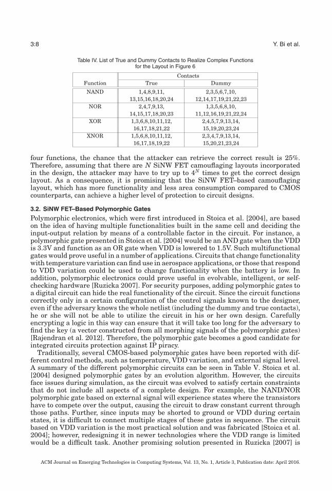
Figure 6 shows a more complex camouflaging gate that can act as NAND, NOR, XOR,or XNOR given different sets of dummy contacts. As described in Table IV, different
ACM Journal on Emerging Technologies in Computing Systems, Vol. 13, No. 1, Article 3, Publication date: April 2016.
Emerging Technology-Based Design of Primitives for Hardware Security 3:7
Fig. 5. Camouflaging layout performing NAND or NOR.
Table III. List of True and Dummy Contacts to Realize BasicFunctions for the Layout in Figure 5
ContactsFunction True Dummy
NAND 1,2,4,5,10 3,6,7,8,9NOR 3,6,7,8,9 1,2,4,5,10
Fig. 6. Camouflaging layout with four possible functions: NAND, NOR, XOR, or XNOR.
connections can result in four different operations for the same input signals. Again,only four SiNW FETs are used in this camouflaging gate. Compared to the CMOS-based camouflaging gate, which needs 12 transistors for a NAND-NOR-XOR gate, theproposed circuit structure can reduce two-thirds of the transistor count. However, fivemore contacts are used in the SiNW FET–based camouflaging gate, although the areaoverhead incurred by the extra contacts are negligible considering the transistor countreduction. To further evaluate the security improvement, the security metric has beenused to check how easily an attacker can guess the full functionality of given designscontaining camouflaging gates. In other words, if one camouflaging layout can achieve
ACM Journal on Emerging Technologies in Computing Systems, Vol. 13, No. 1, Article 3, Publication date: April 2016.
3:8 Y. Bi et al.
Table IV. List of True and Dummy Contacts to Realize Complex Functionsfor the Layout in Figure 6
four functions, the chance that the attacker can retrieve the correct result is 25%.Therefore, assuming that there are N SiNW FET camouflaging layouts incorporatedin the design, the attacker may have to try up to 4N times to get the correct designlayout. As a consequence, it is promising that the SiNW FET–based camouflaginglayout, which has more functionality and less area consumption compared to CMOScounterparts, can achieve a higher level of protection to circuit designs.
3.2. SiNW FET–Based Polymorphic Gates
Polymorphic electronics, which were first introduced in Stoica et al. [2004], are basedon the idea of having multiple functionalities built in the same cell and deciding theinput-output relation by means of a controllable factor in the circuit. For instance, apolymorphic gate presented in Stoica et al. [2004] would be an AND gate when the VDDis 3.3V and function as an OR gate when VDD is lowered to 1.5V. Such multifunctionalgates would prove useful in a number of applications. Circuits that change functionalitywith temperature variation can find use in aerospace applications, or those that respondto VDD variation could be used to change functionality when the battery is low. Inaddition, polymorphic electronics could prove useful in evolvable, intelligent, or self-checking hardware [Ruzicka 2007]. For security purposes, adding polymorphic gates toa digital circuit can hide the real functionality of the circuit. Since the circuit functionscorrectly only in a certain configuration of the control signals known to the designer,even if the adversary knows the whole netlist (including the dummy and true contacts),he or she will not be able to utilize the circuit in his or her own design. Carefullyencrypting a logic in this way can ensure that it will take too long for the adversary tofind the key (a vector constructed from all morphing signals of the polymorphic gates)[Rajendran et al. 2012]. Therefore, the polymorphic gate becomes a good candidate forintegrated circuits protection against IP piracy.
Traditionally, several CMOS-based polymorphic gates have been reported with dif-ferent control methods, such as temperature, VDD variation, and external signal level.A summary of the different polymorphic circuits can be seen in Table V. Stoica et al.[2004] designed polymorphic gates by an evolution algorithm. However, the circuitsface issues during simulation, as the circuit was evolved to satisfy certain constraintsthat do not include all aspects of a complete design. For example, the NAND/NORpolymorphic gate based on external signal will experience states where the transistorshave to compete over the output, causing the circuit to draw constant current throughthose paths. Further, since inputs may be shorted to ground or VDD during certainstates, it is difficult to connect multiple stages of these gates in sequence. The circuitbased on VDD variation is the most practical solution and was fabricated [Stoica et al.2004]; however, redesigning it in newer technologies where the VDD range is limitedwould be a difficult task. Another promising solution presented in Ruzicka [2007] is
ACM Journal on Emerging Technologies in Computing Systems, Vol. 13, No. 1, Article 3, Publication date: April 2016.
Emerging Technology-Based Design of Primitives for Hardware Security 3:9
Table V. Summary of Developed Polymorphic Gates
Function Morph MethodNumber ofTransistors Where Published
AND/OR 27/125 C Temperature 6 Stoica et al. [2001]AND/OR/XOR 3.3/0.0/1.5V External
signal10 Stoica et al. [2001]
AND/OR 3.3/0.0V External signal 6 Stoica et al. [2001]NAND/NOR/XOR/AND 0.0/0.9/1.1/1.8V External
signal11 Stoica et al. [2001]
AND/OR 1.2/3.3V Vdd 8 Stoica et al. [2001]NAND/NOR 3.3/1.8V Vdd 6 (Fabricated) Stoica et al. [2004]NAND/XOR 0/3.3V External signal 9 Ruzicka [2007]NAND/NOR VDD and GND
interchange4 This work
Fig. 7. (a) SiNW FETs NAND. (b) CMOS NAND.
Fig. 8. (a) SiNW FETs NOR. (b) CMOS NOR.
a NAND/XOR gate controlled by a control signal using nine transistors. The gate hasgood performance even when we redesigned it in the 22nm FinFET technology node.
Here we present a novel approach to designing polymorphic gates using polarity-controllable FETs. The ability to control the polarity of a transistor enables us to buildpolymorphic cells with a much less number of transistors. As shown in Figures 7 and 8,the basic NAND and NOR gate structure is similar for both the CMOS and the SiNWFET. The polarity control gate does not reduce the number of transistors required toimplement NAND and NOR using SiNW FET technology. However, this unique prop-erty allows us to change the functionality of the gate simply by interchanging the
ACM Journal on Emerging Technologies in Computing Systems, Vol. 13, No. 1, Article 3, Publication date: April 2016.
3:10 Y. Bi et al.
Table VI. Simulation Results for NAND/NOR Gates
Average DynamicPower for Output
Switching at 1GHz Delay Averaged onGate Static Power (pW) (uW) Different Transitions (ps)
FinFET 22nm LSTP NOR 52.19 0.19 28FinFET 22nm HP NOR 30360 0.67 23.5FinFET 22nm LSTP NAND 27.19 0.15 23FinFET 22nm HP NAND 1650 0.652 15.5SiNW FET 20nm NAND/NOR 8.037 1.77 42SiNW FET 20nm NAND/NOR 4.127 1.13 56
Fig. 9. Original functionality of a SiNW FET complex gate. (a) Transistor schematic. (b) Gate schematic.
VDD and GND. Note that interchanging the VDD and GND connections in any CMOS-based logic will produce the complement of the original function at the output, but fullvoltage swing at the output will not be achieved due to the presence of PMOS in thepull-down network or NMOS in the pull-up network. Therefore, using this method, onecan gather the VDD and GND terminals of the NAND and NOR gates in a combina-tional logic into a vector and construct a “logic encryption key.” As opposed to the workpresented in Rajendran et al. [2012], which adds additional XOR or XNOR gates intoa logic gate to realize the logic encryption scheme and thus incurs performance over-head, this approach has zero overhead in terms of gate count and trivial wiring costdue to the switching of VDD/GND. The comparison of transistor counts for differentpolymorphic gates is listed in Table V.
The simulation results for the NAND and NOR generic cells using the EPFL SiNWFET model [Gaillardon et al. 2014b] and the FinFET 22nm low standby power (LSTP)and high performance (HP) configurations of the PTM model [Arizona State University2014] can be viewed in Table VI. It is not surprising to see that SiNW FET–based NAND(or NOR) gate consumes more dynamic power and has longer delay than the CMOSNAND (or NOR) gate, mainly because of the immaturity of the SiNW FET technology.Note that the leakage power of the SiNW FET is drastically reduced compared to thatof FinFET technology.
The performance comparison in Table VI does not take the SiNW FET unique prop-erty into consideration. In fact, the benefits of using SiNW FETs can be revealed ifthe polarity-controllable property is leveraged (e.g., sophisticated polymorphic gates).To validate our claim, a sample polymorphic gate is designed (Figure 9). The two sep-arate functions shown in Figures 9(b) and 10(b) can be implemented by the SiNWFET circuit in its different VDD and GND configurations depicted in Figures 9(a) and10(a). Table VII lists the simulation results of the designed SiNW FET polymorphiclogic and a MUX-based CMOS polymorphic gate that achieves the same functionality.
ACM Journal on Emerging Technologies in Computing Systems, Vol. 13, No. 1, Article 3, Publication date: April 2016.
Emerging Technology-Based Design of Primitives for Hardware Security 3:11
Fig. 10. Reconfigured functionality of a SiNW FET complex gate. (a) Transistor schematic. (b) Gateschematic.
Table VII. Simulation Results of the SiNW FET and CMOS Five-Input Polymorphic Function
Technology Static Power (nW) Switching Average Power (uW) Average Delay (ps)
As the results suggest, the SiNW FET approach reduces the total dynamic power dueto the fewer number of cells while suffering from a longer delay because of the samenumber of cells available in the critical path. Besides the extremely low leakage power,the overall performance of the SiNW FET polymorphic logic is better than its CMOScounterpart. Consequently, SiNW FET circuits outperform CMOS circuits in termsof power and delay while achieving a similar level of circuit protection. The securitymetric that we applied measures the difficulty level if attackers want to learn the cir-cuit structure using the brute force method. In other words, if there are N gates eachwith two possible functions in the schematic, it would take 2N trials for an attacker todetermine the exact functionality of the circuit. The benefits can be more significantin more complex polymorphic logic for large-scale circuits protection. We would like topoint that machine learning attacks may be used to speed up the hacking of encryption[Baumgarten et al. 2010]. Thus, judicious placement of these SiNW FET polymorphicgates in a circuit should also be considered to impede such attacks.
3.3. Graphene SymFET–Based Circuit Protectors
Besides the IP protection mentioned previously, emerging devices may also help toimprove circuit resilience to counter various hardware attacks, such as fault injectionand side-channel signal analysis, with extremely low performance overhead and littlecircuit redesign. For example, cryptographic circuits are often vulnerable to powersupply–based fault injections [Barenghi et al. 2010]. The manipulation of the powersupply causes faults due to the rise of the setup time needed for registers to switch intothe correct state: this phenomenon particularly affects high-capacitance paths, whichare often the slowest paths of the circuit. In this section, we introduce two SymFET-based circuit protectors that leverage the unique I-V characteristics of SymFETs toprotect circuits from power supply fault injections.
3.3.1. Current-Based Circuit Protector. As shown in Figure 2, the I-V curve of a SymFETindicates that the IDS only exists for a narrow band of VDS. Supported by this property,we propose a current-based circuit protector, which can effectively prevent supplyvoltage–based fault injection. Figure 11 shows the proposed structure relying on theunique properties of SymFETs. As shown in the schematic, SymFET M1 is the only
ACM Journal on Emerging Technologies in Computing Systems, Vol. 13, No. 1, Article 3, Publication date: April 2016.
3:12 Y. Bi et al.
Fig. 11. Schematic of a current-based circuit protector.
Fig. 12. Simulation of output current changing with VDD.
Table VIII. Power Provided by a Current-Based Circuit Protector
transistor directly connected to the power supply VDD, which is also the source tolaunch a voltage-based fault injection attack.
We use a specific parameter setting to explain how the circuit protector works. Inour experiment, VT G is set to 0.6V and VBG is set to 0V for all three SymFETs. Thesegate voltages can be adjusted so that the peak current will appear in different powersupply ranges than the one shown in Figure 12. Since M2 and M3 are connected inparallel, source-to-drain voltage VDS2 for M2 is equal to VDS3 for M3, which makesthe output current IOU T the same as the input current IIN. The output current IOU Tis basically a current source for the circuit under protection. For this SymFET-basedcircuit protector, the output current can only exist for a specific drain-source voltage ofSymFET M3. If VDS3 is out of this range, either higher or lower than the predefinedrange, the SymFET M3 will be cut off. As a consequence, the circuit under protectionwill be totally shut down.
The simulation results of the current-based circuit protector in Figure 12 show thatonly if the VDD is in the range from 0.8V to 1V, the output current will be at its peakvalues (e.g., 1.928uA when VDD is 1V). The power consumption is also derived andlisted in Table VIII. When the supply voltage deviates from its normal value (e.g., 0.6V),the output current will drop down to 0.176uA. This feature can be directly exploited
ACM Journal on Emerging Technologies in Computing Systems, Vol. 13, No. 1, Article 3, Publication date: April 2016.
Emerging Technology-Based Design of Primitives for Hardware Security 3:13
in circuit protection, countering side-channel attacks and fault injections. However,due to the limited maximum current, the current protector can mainly be appliedfor relatively lightweight cryptographic circuits to prevent fault injections. To handlerelatively larger loads, either larger SymFET devices or multiple protectors are needed.If the attackers intend to lower the supply voltage to trigger a single-bit error of anencryption design, the entire circuit can be automatically shut down by the proposedcircuit protector before a single-bit error could occur.
Traditionally, power regulators are often used in CMOS technology to protect themain circuit, but they suffer from large area and power consumption. For example,Guo and Leung [2010] proposed an area-efficient regulator based on the 90nm CMOStechnology. The regulator includes more than 20 transistors, three capacitors, and oneresistor with a total area of 0.019mm2 and power consumption of 6μW. However, inour proposed structure, only three SymFET transistors are utilized, leading to an areareduction even though one SymFET consumes larger area than one MOSFET in asimilar process. The main drawback of the designed circuit protector is the positivevoltage at the virtual ground of the main circuit (i.e., the drain voltage of M3 may belarger than 0V). However, the proposed circuit protector can be used as an alternativeto the current source, which acts as both a current source and a circuit protector [Liet al. 2014].
3.3.2. Voltage-Based Circuit Protector. Besides the current-based circuit protector, whichprotects the circuit through current manipulation, SymFETs can also be used to controlthe supply voltage for fault injection prevention. Figure 13(a) shows the schematic of theproposed voltage-based circuit protector, which is similar to an inverter design [Sedighiet al. 2014b]. However, in this circuit protector, the top gates of the two SymFETs areconnected to the voltage source, whereas VB can be manipulated for different cut-offvoltage levels for output Vout. For instance, in Figure 13(b), in the case of VB equal to0.8V, the output voltage quickly drops to nearly zero when VDD is lowered down to0.65V, therefore cutting off the voltage supply for the circuit under protection.
To further demonstrate the functionality of the proposed circuit protector, a fulladder in the 20nm FinFET technology combined with the protector is implemented andsimulated as shown in Figure 14. Note that since the current SymFET technology is notCMOS compatible, 3D stacking is needed to protect a CMOS circuit with the developedprotector. That said, we have shown the feasibility of building digital circuits (Inverter,NAND, NOR, etc.) using SymFETs in Sedighi et al. [2014b]. Thus, one can ultimately
ACM Journal on Emerging Technologies in Computing Systems, Vol. 13, No. 1, Article 3, Publication date: April 2016.
3:14 Y. Bi et al.
Fig. 14. Voltage-based circuit protector on a one-bit full adder. (a) Schematic. (b) Simulation results.
Table IX. Power Measurement of a SymFET Voltage-Based Circuit Protector
Power of the protector (nW) 250.5 135.7 142.9 110.3 76.1 30.3 5.9 0.4Power of the full adder (nW) 310.9 117.0 1.0 <0.03 <0.02 <0.02 <0.02 <0.02
envision a chip comprised entirely of SymFETs. One input of the full adder is set to logic“1,” and the other input is given as a periodic pulse signal. As we can see in Figure 14(b),the universal VDD is manipulated to decrease gradually. When it reaches 0.65V, theoutput voltage of the circuit protector quickly drops to zero. Consequently, both the sumand carry-out in the full adder output zero. We also measured the power consumptionby the circuit protector and summarized the results in Table IX. Because the dynamicpower is frequency dependent, input switching is set at 1GHz in the simulation. Theleakage current shown here is the current flowing through the two SymFETs insteadof the circuit under protection. As shown in Table IX, when the power supply is largeenough to make the full adder operate normally, power consumption by the full adderdominates the overall power consumption. However, if the full adder is completely shutoff when the supply voltage becomes lower than 0.65V, the majority of the total poweris attributed to the static power of the circuit protector. Although high leakage maynot be desired in low-power applications, for circuit protection purposes, the poweroverhead is bearable as long as it can prevent the intentional injection from the supplyvoltage. More research is needed along this direction to lower the leakage power.
Gomina et al. [2014] evaluated the impacts of power supply attacks where the voltagesensitivity margin is 0.4V. In other words, a bit flip error would only happen if the powersupply glitch were larger than 0.4V. In what we have presented, the voltage sensitivityof our designs is less than 0.2V. Before the power glitch attack can be triggered, theSymFET circuit protector already shuts down the circuit to prevent such attacks. Notethat the sensitivity of the SymFET projector can be adjusted by altering the top/backgate voltages. Another factor to consider is noise in the power supply. It may be possiblethat due to environmental variations (e.g., temperature variation and power noise), thesupply voltage may fluctuate. If the voltage variation is larger than the design margin,a false alarm will be triggered and the circuit will be shut down even though no attacksare launched. For circuits working under extreme conditions, we may need to tune thecircuit protector to increase the allowed supply voltage noise margin.
ACM Journal on Emerging Technologies in Computing Systems, Vol. 13, No. 1, Article 3, Publication date: April 2016.
Emerging Technology-Based Design of Primitives for Hardware Security 3:15
Fig. 15. Schematic of the SymFET XOR logic.
Fig. 16. Simulation results of the SymFET XOR logic.
3.4. Graphene SymFET–Based XOR Logic
In the cryptographic systems, XOR logic serves as a basic computation unit for manyof the encryption algorithms. Since CMOS XOR gates often take at least eight transis-tors, area and power consumption of XOR network becomes the bottleneck to furtherimprove the performance of cryptographic designs. However, in terms of the uniqueI-V characteristic and low-power feature, the SymFET brings in a new opportunity forhardware security implementation. In Sedighi et al. [2014b], a group of SymFET-basedgeneric logic gates have been investigated, such as inverter, NAND, and majority gates.
Following a similar design method, a lightweight current-based XOR gate is thendeveloped that uses only two SymFETs. In Figure 15, the V tg of the upper SymFET isconnected to input signal A, whereas the Vbg is connected to input signal B. The drainand source of the upper SymFET are connected to the voltage supply and the outputport, respectively. In the lower SymFET, the Vtg and Vbg are tied up to complement Aand complement B, respectively. The drain and source connections of the lower SymFETare the same as the upper one. The simulation results are shown in Figure 16, whichillustrates that when input signals A and B are different, there will be a steady outputcurrent through the output port. When A and B are of equal value, the output currentdrops to nearly zero. In this demonstration, input signals are set as square pulseswith the peak voltage of 2V, whereas the supply voltage remains at 500mV. Since thepeak current happens due to the different configurations of drain-source voltage and
ACM Journal on Emerging Technologies in Computing Systems, Vol. 13, No. 1, Article 3, Publication date: April 2016.
3:16 Y. Bi et al.
Table X. Summary of SiNW FET and SymFET in Security Applications
SiNW FETs Graphene SymFETs
Benefits over CMOSPolarity configurable, low static power, Low power, built-in
fewer transistors for applications negative differential resistance
ChallengesLarger area per-transistor, Current-based designs,
other security applications cryptographic circuits
gate voltage (see Figure 2), the design also works with the settings of lower VDD andtop/back gate voltage through the same configuration on all terminals.
To fully compare the performance between CMOS XOR and SymFET XOR, delayand power consumption of both gates are also measured. We implemented an eight-transistor XOR gate in CMOS 130nm technology with the nominal voltage of 1.5V[Sedighi et al. 2014b]. (The 130nm CMOS technology is chosen since this feature sizeis close to the feature size used by the SymFET device: 100 × 100 nm.) The CMOS XORgate consumes 0.632μW. Although the SymFET-based XOR gate consumes 0.68μW,both gates are comparable in power consumption. However, the average delay of theSymFET XOR gate is 48ps. Compared to the 135ps delay of the CMOS XOR gate,the speed of the SiNW FET XOR gate is much faster. With slightly larger powerconsumption, the SymFET XOR gate outperforms the CMOS XOR gate significantlyin delay and area. Moreover, the power consumption of the SymFET XOR gate can befurther reduced by lowering the nominal voltage to less than 2.0V.
Although the XOR gate is the basic gate for many cryptographic circuits, othergates (e.g., inverter and NAND gates) may also be required. Sedighi et al. [2014b] andGaillardon et al. [2014a] have already developed logic gates using SymFET and SiNWFET, respectively. Therefore, the developed XOR gate along with other logic gates canmake the cryptographic circuits perform better than their CMOS counterparts.
4. DISCUSSION
Emerging technologies, acting as alternatives to CMOS logic, have already shownpromising features for high-performance circuit design. However, the metrics to eval-uate different technologies often follow the traditional criteria, focusing only on power,delay, area, and so forth for general-purpose computation modules. Special applica-tions, such as hardware security, are rarely considered, mainly because MOSFETs donot support security and circuit protection naturally.
In this article, we presented security primitives on how the unique features of emerg-ing technologies can help to protect circuits and prevent IP piracy. Unlike CMOS logic,the proposed protection schemes are of much lower overhead because security is not anadd-on feature but a built-in feature. Through the simulation results, the two exam-ple devices proved to be efficient in hardware security applications. These preliminaryresults lead us toward a new metric for the comparison between CMOS logic andemerging technologies. Whereas traditional metrics, such as power and delay, are themajor criteria to evaluate the merits of emerging devices, in this work, we include thesecurity metric in the overall performance evaluation to fully compare the emergingdevices with CMOS technology. A summary of the two emerging devices in hardwaresecurity applications is shown in Table X, which lists the benefits and challenges ofthe emerging-device–based designs compared to CMOS designs and can help to guidefuture designs in the hardware security area.
ACM Journal on Emerging Technologies in Computing Systems, Vol. 13, No. 1, Article 3, Publication date: April 2016.
Emerging Technology-Based Design of Primitives for Hardware Security 3:17
5. CONCLUSIONS
Emerging technologies were investigated in this article for their applications in thehardware security domain. Instead of simply replacing CMOS transistors with emerg-ing devices, our work, for the first time, evaluated the unique properties of new devicesin helping protect circuit designs and countering IP piracy. Two emerging technolo-gies were used: SiNW FETs and graphene SymFETs. Five different security applica-tions were designed and verified, ranging from IP protection to efficient cryptographiccomputation. Through our examples, we demonstrated that the unique properties ofemerging technologies, if used properly, can provide high-level circuit protection withextremely low performance overhead. Along this direction, new evaluation metrics willbe developed in our future work to better evaluate the merits of emerging devices.Besides the simulation results, as emerging technologies become more mature, mea-surements from fabricated devices will also be collected to verify the claim thatcircuitprotection methods can benefit from emerging technologies.
REFERENCES
D. Agrawal, S. Baktir, D. Karakoyunlu, P. Rohatgi, and B. Sunar. 2007. Trojan detection using IC finger-printing. In Proceedings of the IEEE Symposium on Security and Privacy. 296–310.
Yousra Alkabani and Farinaz Koushanfar. 2007. Active hardware metering for intellectual property protec-tion and security. In Proceedings of the USENIX Security Conference. 291–306.
J. Appenzeller, J. Knoch, E. Tutuc, M. Reuter, and S. Guha. 2006. Dual-gate silicon nanowire transistors withnickel silicide contacts. In Proceedings of the International Electron Device Meeting (IEDM’06). 1–4.
Arizona State University. 2014. PTM Model. Retrieved March 18, 2016, from http://ptm.asu.edu/.A. Barenghi, G. M. Bertoni, L. Breveglieri, M. Pellicioli, and G. Pelosi. 2010. Fault attack on AES with single-
bit induced faults. In Proceedings of the 2010 6th International Conference on Information Assuranceand Security (IAS’10). 167–172.
A. Baumgarten, A. Tyagi, and J. Zambreno. 2010. Preventing IC piracy using reconfigurable logic barriers.IEEE Design Test of Computers 27, 1, 66–75.
Y. Bi, P.-E. Gaillardon, X. S. Hu, M. Niemier, J.-S. Yuan, and Y. Jin. 2014. Leveraging emerging technologyfor hardware security—case study on silicon nanowire FETs and graphene SymFETs. In Proceedings ofthe 2014 IEEE 23rd Asian Test Symposium (ATS’14). 342–347.
L. Britnell, R. V. Gorbachev, A. K. Geim, L. A. Ponomarenko, A. Mishchenko, M. T. Greenaway, T. M. Fromhold,K. S. Novoselov, and L. Eaves. 2013. Resonant tunnelling and negative differential conductance ingraphene transistors. Nature Communications 4, 1794. http://dx.doi.org/10.1038/ncomms2817.
Lap-Wai Chow, James Baukus, and William Clark. 2002. Integrated circuits protected against reverse engi-neering and method for fabricating the same using an apparent metal contact line terminating on fieldoxide. Patent US 7294935 B2. http://www.google.com/patents/US7294935.
Lap Wai Chow, James P. Baukus, Bryan J. Wang, and Ronald P. Cocchi. 2012. Camouflaging a standard cellbased integrated circuit. Patent US 8151235 B2. http://www.google.com/patents/US8151235.
A. Colli, S. Pisana, A. Fasoli, J. Robertson, and A. C. Ferrari. 2007. Electronic transport in ambipolar siliconnanowires. Physica Status Solidi (b) 244, 11, 4161–4164.
M. De Marchi, D. Sacchetto, S. Frache, J. Zhang, P.-E. Gaillardon, Y. Leblebici, and G. De Micheli. 2012.Polarity control in double-gate, gate-all-around vertically stacked silicon nanowire FETs. In Proceedingsof the 2012 IEEE International Electron Devices Meeting (IEDM’12). 8.4.1–8.4.4.
Frontier Economics. 2011. Estimating the Global Economic and Social Impacts of Counterfeiting and Piracy.Technical Report. Frontier Economics Ltd., London, England.
Pierre-Emmanuel Gaillardon, Luca Amaru, Jian Zhang, and Giovanni De Micheli. 2014a. Advanced systemon a chip design based on controllable-polarity FETs. In Proceedings of the Conference on Design,Automation, and Test in Europe (DATE’14).
P.-E. Gaillardon, S. Bobba, M. De Marchi, D. Sacchetto, and G. De Micheli. 2014b. Nanowire systems:Technology and design. Philosophical Transactions of the Royal Society of London A 372, 20130102.
A. K. Geim and K. S. Novoselov. 2007. The rise of graphene. Nature Materials 6, 183–191.K. Gomina, J.-B. Rigaud, P. Gendrier, P. Candelier, and A. Tria. 2014. Power supply glitch attacks: Design
and evaluation of detection circuits. In Proceedings of the 2014 IEEE International Symposium onHardware-Oriented Security and Trust (HOST’14). 136–141.
ACM Journal on Emerging Technologies in Computing Systems, Vol. 13, No. 1, Article 3, Publication date: April 2016.
Jianping Guo and Ka Nang Leung. 2010. A 6-μW chip-area-efficient output-capacitorless LDO in 90-nmCMOS technology. IEEE Journal of Solid-State Circuits 45, 9, 1896–1905.
Andre Heinzig, Stefan Slesazeck, Franz Kreupl, Thomas Mikolajick, and Walter M. Weber. 2012. Reconfig-urable silicon nanowire transistors. Nano Letters 12, 1, 119–124.
Digh Hisamoto, Wen Chin Lee, Jakub Kedzierski, Hideki Takeuchi, Kazuya Asano, Charles Kuo, ErikAnderson, Tsu Jae King, Jeffrey Bokor, and Chenming Hu. 2000. FinFET—a self-aligned double-gateMOSFET scalable beyond 20nm. IEEE Transactions on Electron Devices 47, 12, 2320–2325.
ITRS. 2013. Emerging research devices and emerging research materials. In International TechnologyRoadmap for Semiconductors (2013 ed.). ITRS, New York, NY, 43.
A. Iyengar, K. Ramclam, and S. Ghosh. 2014. DWM-PUF: A low-overhead, memory-based security primitive.In Proceedings of the 2014 IEEE International Symposium on Hardware-Oriented Security and Trust(HOST’14). 154–159.
C.-H. Jan, U. Bhattacharya, R. Brain, S.-J. Choi, G. Curello, G. Gupta, W. Hafez, M. Jang, M. Kang, K.Komeyli, T. Leo, N. Nidhi, L. Pan, J. Park, K. Phoa, A. Rahman, C. Staus, H. Tashiro, C. Tsai, P.Vandervoorn, L. Yang, J.-Y. Yeh, and P. Bai. 2012. A 22nm SoC platform technology featuring 3-d tri-gate and high-k/metal gate, optimized for ultra low power, high performance and high density SoCapplications. In Proceedings of the 2012 IEEE International Electron Devices Meeting (IEDM’12).
Y. Jin and Y. Makris. 2008. Hardware Trojan detection using path delay fingerprint. In Proceedings of theIEEE International Workshop on Hardware-Oriented Security and Trust. 51–57.
Y. Jin and D. Oliveira. 2014. Extended abstract: Trustworthy SoC architecture with on-demand security poli-cies and HW-SW cooperation. In Proceedings of the 5th Workshop on SoCs, Heterogeneous Architectures,and Workloads (SHAW-5).
Yier Jin, Bo Yang, and Yiorgos Makris. 2013. Cycle-accurate information assurance by proof-carrying basedsignal sensitivity tracing. In Proceedings of the IEEE International Symposium on Hardware-OrientedSecurity and Trust (HOST’13). 99–106.
X. Li, W.-Y. Tsai, V. Narayanan, H. Liu, and S. Datta. 2014. A low-voltage low-power LC oscillator usingthe diode-connected SymFET. In Proceedings of the 2014 IEEE Computer Society Annual Symposiumon VLSI (ISVLSI’14). 302–307.
Sheng Lin, Yong-Bin Kim, and Fabrizio Lombardi. 2011. CNTFET-based design of ternary logic gates andarithmetic circuits. IEEE Transactions on Nanotechnology 10, 2, 217–225.
Y.-M. Lin, J. Appenzeller, J. Knoch, and P. Avouris. 2005. High-performance carbon nanotube field-effecttransistor with tunable polarities. IEEE Transactions on Nanotechnology 4, 5, 481–489.
H. Lu and A. Seabaugh. 2014. Tunnel field-effect transistors: State-of-the-art. IEEE Journal of the ElectronDevices Society 2, 4, 44–49. DOI:http://dx.doi.org/10.1109/JEDS.2014.2326622
K. S. Ma, H. C. Liu, Y. Xiao, Y. Zheng, X. Q. Li, S. K. Gupta, Y. Xie, and V. Narayanan. 2014. Independently-controlled-gate FinFET 6T SRAM cell design for leakage current reduction and enhanced read ac-cess speed. In Proceedings of the 2014 IEEE International Symposium on Very-Large-Scale Integration(VLSI’14).
R. Martel, V. Derycke, C. Lavoie, J. Appenzeller, K. K. Chan, J. Tersoff, and P. Avouris. 2001. Ambipolarelectrical transport in semiconducting single-wall carbon nanotubes. Physical Review Letters 87, 25,256805.
M. Potkonjak, A. Nahapetian, M. Nelson, and T. Massey. 2009. Hardware Trojan horse detection usinggate-level characterization. In Proceedings of the 46th Annual Design Automation Conference (DAC’09).688–693.
J. Rajendran, Y. Pino, O. Sinanoglu, and R. Karri. 2012. Logic encryption: A fault analysis perspective. InProceedings of the Conference on Design, Automation, and Test in Europe. 953–958.
Jeyavijayan Rajendran, Michael Sam, Ozgur Sinanoglu, and Ramesh Karri. 2013. Security analysis ofintegrated circuit camouflaging. In Proceedings of the 2013 ACM SIGSAC Conference on Computer andCommunications Security (CCS’13). 709–720.
P. Ronald, P. James, and J. Bryan. 2012. Building block for a secure cmos logic cell library. Patent US20100301903 A1. http://www.google.com/patents/US20100301903.
K. Roy, M. Sharad, D. L. Fan, and K. Yogendra. 2014. Computing with spin-transfer-torque devices: Prospectsand perspectives. In Proceedings of the 2014 IEEE International Symposium on Very-Large-Scale Inte-gration (VLSI’14).
R. Ruzicka. 2007. New polymorphic NAND/XOR gate. In Proceedings of 7th WSEAS International Conferenceon Applied Computer Science, Vol. 2007. 192–196.
ACM Journal on Emerging Technologies in Computing Systems, Vol. 13, No. 1, Article 3, Publication date: April 2016.
Emerging Technology-Based Design of Primitives for Hardware Security 3:19
Alan C. Seabaugh and Qin Zhang. 2010. Low-voltage tunnel transistors for beyond CMOS logic. Proceedingsof the IEEE 98, 12, 2095–2110. DOI:http://dx.doi.org/10.1109/JPROC.2010.2070470
B. Sedighi, X. S. Hu, J. J. Nahas, and M. Niemier. 2014a. Nontraditional computation using beyond-CMOStunneling devices. IEEE Journal on Emerging and Selected Topics in Circuits and Systems 4, 4, 438–449.
B. Sedighi, Xiaobo Sharon Hu, Joseph J. Nahas, and M. Niemier. 2014b. Boolean circuit design using emergingtunneling devices. In Proceedings of the International Conference on Computer Design (ICCD’14). 355–360.
Arvind Seshadri, Mark Luk, Ning Qu, and Adrian Perrig. 2007. SecVisor: A tiny hypervisor to providelifetime kernel code integrity for commodity OSes. In Proceedings of the 21st ACM SIGOPS Symposiumon Operating Systems Principles (SOSP’07). 335–350.
A. Stoica, R. S. Zebulum, and D. Keymeulen. 2001. Polymorphic Electronics. Springer.A. Stoica, R. S. Zebulum, D. Keymeulen, M. I. Ferguson, and V. Duong. 2004. Taking evolutionary circuit
design from experimentation to implementation: Some useful techniques and a silicon demonstration.IEE Proceedings—Computers and Digital Techniques 151, 4, 295–300.
P. Zhao, R. M. Feenstra, Gong Gu, and D. Jena. 2013. SymFET: A proposed symmetric graphene tunnel-ing field-effect transistor. IEEE Transactions on Electron Devices 60, 3, 951–957. DOI:http://dx.doi.org/10.1109/TED.2013.2238238
Received December 2014; revised August 2015; accepted August 2015
ACM Journal on Emerging Technologies in Computing Systems, Vol. 13, No. 1, Article 3, Publication date: April 2016.