http://www.semiconductorsimulation.comhttp://[email protected] or cell 847-624-7907
2 EMI-EMC, February 2011
Key Points�“Right the First Time�” is an optimum way to design equipmentAvoiding problems requires insight and planningFront-end design requires modeling and simulationEMI-EMC is getting harder to do because of faster ICsAdvanced bypassing techniques are needed for PI and I/OsAdvanced crosstalk control eliminates split planesEMI-EMC insight is enabled by advanced computational toolsVerify your assumptions with measurements and simulationsExperience and reflection improve insight, foresight, and skill
3 EMI-EMC, February 2011
Partial Redesign of a Microprocessor Board
OriginalOriginal BoardBoard
�•What was done: Clock nets were simulated and terminated. Floating planes were grounded and layout improved. Result.�•What was missed: elimination of moats and splits, proper bypassing, and replacement of single, unshielded connector for all I/Os. Do you think more could have been accomplished?
RedesignedRedesigned BoardBoard
Complexity versus Simplification in Modeling & Simulation
5 EMI-EMC, February 2011
An Example of a Complex Network
An 18-Slot Bi-Directional Backplane Bus. Courtesy of 3Com. Used with permission
6 EMI-EMC, February 2011
Simulation Results from too Simple a Model
Complex nets are hard to terminate and have many reflectionsSimple dV/dt modeling and device behavior is inadequate for accurate resultsV-T curves need to be modeled for correct results in GTL/GTLP busses
7 EMI-EMC, February 2011
IBIS Modeling of V-T Curves:How GTLP Drivers Really Behave
This slide shows how to correctly model GTL/GTLPSoft turn-on/turn-off removes many high-frequency components (think about Fourier transformation) from driving the lineThe results of the change in modeling detail are shown next:
8 EMI-EMC, February 2011
Better Models Give Better Results
�“Everything should be as simple as possible and no simpler.�”
Albert Einstein
9 EMI-EMC, February 2011
Semiconductor Technology Roadmap
Slide courtesy of Etienne Sicard, University of INSA-Toulouse. Used with permission
10 EMI-EMC, February 2011
PI and the IEC 62014-3 Proposal
Proposed IEC 62014-3 core switching noise coupling model
Slide courtesy of Etienne Sicard, INSA-Toulouse
Signal Integrity and EMI-EMC
12 EMI-EMC, February 2011
Test Net for SI and EMI
66MHz Clock Topology as Modified
13 EMI-EMC, February 2011
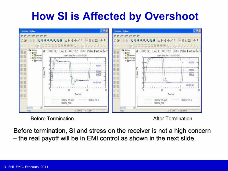
How SI is Affected by Overshoot
Before TerminationBefore Termination After TerminationAfter Termination
14 EMI-EMC, February 2011
How EMI is Affected by Overshoot
Before TerminationBefore Termination After TerminationAfter Termination
The SI Engineer has to manage harmonics out to about the 5The SI Engineer has to manage harmonics out to about the 5thth . . The EMI engineer has to manage harmonics out to, perhaps, the 10The EMI engineer has to manage harmonics out to, perhaps, the 1000thth..
15 EMI-EMC, February 2011
Example of Virtual Test Board
Stackup of the Test Board Layout of the Test Board
The board on the left has the following stackup:
top: 1.2 mil Cu signal Zo = 89next: 12 mil FR4 ( r = 4.5)next: 1.2 mil Cu shield Vccnext: 12 mil FR4next: 1.2 mil Cu shield GNDnext: 12 mil FR4bottom: 1.2 mil Cu signal Zo = 89Etch width is nominally 6 mils
For the shielded version outer shield layers of 1.2 mil Cu spaced by 12 mils of FR4 were added
The nominal 6 mil etch on such an inner layer results in Zo = 59.6
The board is about 3 inches long.
16 EMI-EMC, February 2011
Virtual Test Board Before and After EMI Treatment
Shielded, Terminated, Constant Impedance Net
Unshielded, Unterminated, Non-Constant Impedance Net
Power Integrity (PI) and EMI-EMC
18 EMI-EMC, February 2011
Power Bounce (& Ground) Basics
Distributed: vR = iR, vC = iXC, vL = iXL, XC = -j/2 fC, XL = j2 fLSwitch characteristics: V-I & V-T curves, pin parasitics, etc. See the IBIS Model.
R XL
XC
load
XC
R XL
powerplane
returnpowerplane
19 EMI-EMC, February 2011
Bypassing the Power Supply for PI
Slide courtesy of Lee Ritchey, Speeding Edge. Used with permission.
20 EMI-EMC, February 2011
Interplane Capacitance
Slide courtesy of Lee Ritchey, Speeding Edge. Used with permission.
21 EMI-EMC, February 2011
Splitting Ground Planes: An Example
Analog ground plane and digital ground plane were �“stitched�”together at 9 locations on this PCB
This change was done to improve both radiated emissions and susceptibility (300 �– 400 MHz)
A stitch with 30 GA wire
22 EMI-EMC, February 2011
Before StitchingRadiated EmissionsR
23 EMI-EMC, February 2011
After StitchingRadiated Emissions
24 EMI-EMC, February 2011
Stripline Crosstalk
Slide courtesy of Lee Ritchey, Speeding Edge. Used with permission.
25 EMI-EMC, February 2011
Observations About CrosstalkAbove audio (10kHz) electromagnetic energy stays very close to a wire it is flowing on when its reference plane is close.
Electromagnetic near field coupling strength falls off at about 1/(distance)3. At 10 mils away from a trace 5 mils from a reference plane less than 5% crosstalk coupling is detectable.
Split planes, rows of ground vias around a PCB perimeter, guard traces, and edge plating to control crosstalk coupling and EMI should be closely critiqued when frequencies are above audio.
Board Level EMI-EMC
Visualization Using Computational Electromagnetics Tools
27 EMI-EMC, February 2011
Near Field EMI SimulatorsA compact model (E-H vectors, etc.) is extracted for use in CEM tools at the next level up amongst all mainstream EDA vendors
See also: EMScan
Image Courtesy of Johnson Controls Automotive, Inc. Used with permission
Line Replaceable Module Level EMI-EMC
Computation and Visualization with CEM Tools
29 EMI-EMC, February 2011
3D Full-Wave EMI SimulatorsBaseline Ground Pins Only
Pins and StandoffsStrong Coupling
to Slot-WHY?Standoffs Only
30 EMI-EMC, February 2011
Example: Non-CEM Tools: Shielding Effectiveness of Holes
Slide courtesy of IEEE and Bruce Archambeault. Used with permission
System/Sub-System Level EMI-EMC
Visualizing the Test Chamber with CEM Tools
32 EMI-EMC, February 2011
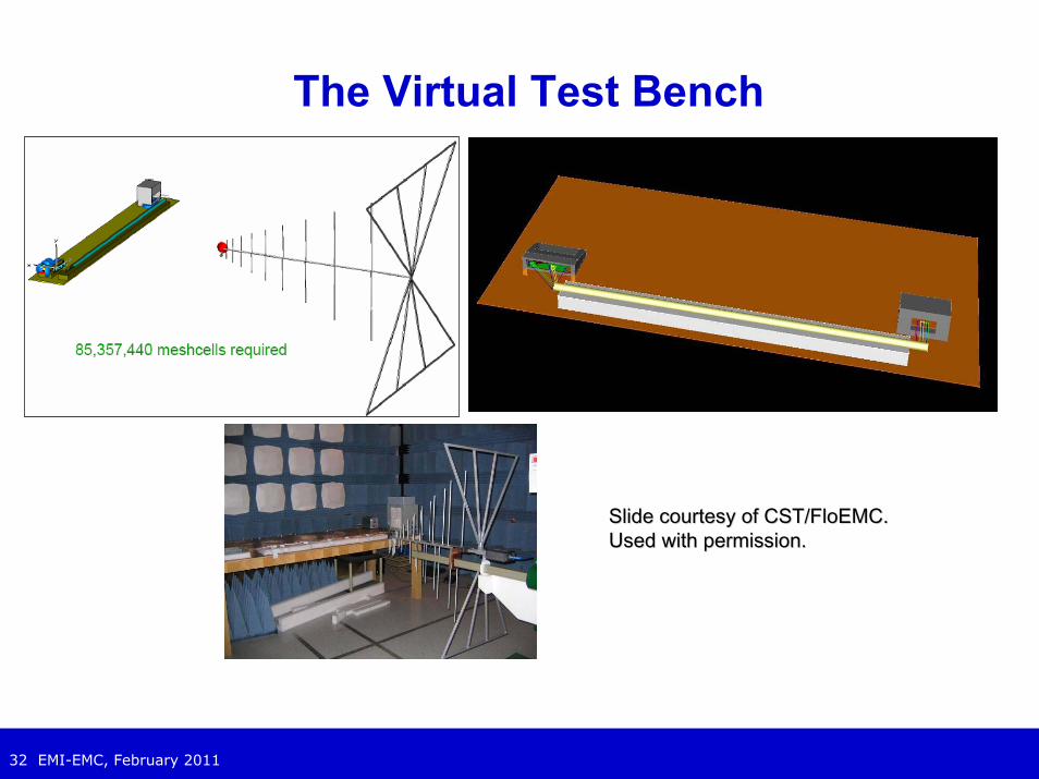
The Virtual Test Bench
33 EMI-EMC, February 2011
Simulation vs. MeasuredBare PCB w/ cable vs. Shielded PCB w/ cable
Shielded PCB w/ cable
Bare PCB w/ cable
Increased high
frequency emissions
Bare PCB w/ cable
Shielded PCB w/ cable
Simulated emissions (broadband source)
Reduced low frequency emissions
Slide courtesy of CST of America. Used with permission.Presented at IEEE EMC 2008 Symposium Measured emissions (30 MHz CLK)
34 EMI-EMC, February 2011
Far-Field EMI SimulatorsSimulators of this type help the visualization of issues raised Simulators of this type help the visualization of issues raised in the previous in the previous slide
35 EMI-EMC, February 2011
Active Rod Setup
The active rod monopole antenna, its counterpoise, the ground plane resonances, and the room resonances all interact
�“Surprises�” in EMI Test Chambers
37 EMI-EMC, February 2011
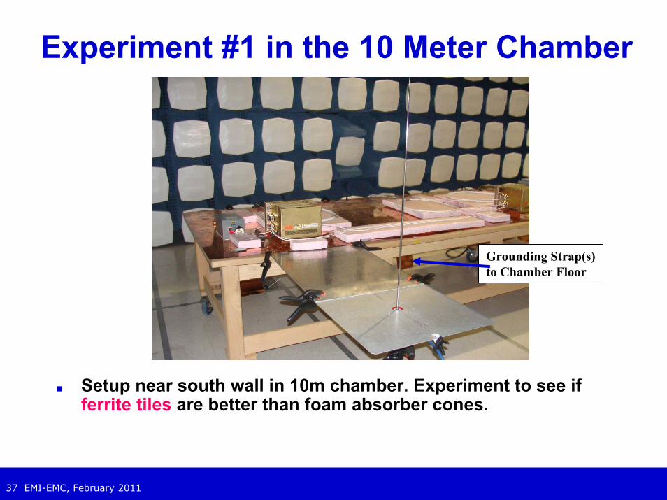
Experiment #1 in the 10 Meter Chamber
Grounding Strap(s) to Chamber Floor
Setup near south wall in 10m chamber. Experiment to see if ferrite tiles are better than foam absorber cones.
38 EMI-EMC, February 2011
10 Meter Chamber South Wall ResultRadiated Emissions
Initially, HF band spurs are 25 dB worse than in MIL461 chamber!!!
39 EMI-EMC, February 2011
10 Meter Chamber East Wall ResultRadiated Emissions
HF band spurs have immediately dropped 15 to 25 dB! Copper bench top still ground strapped to chamber floor.
40 EMI-EMC, February 2011
Model Suggested by Measurements Resonances and impedances of the PCB, Line Replaceable Module, test bench, grounding system, cables and test room all interact just the same as elements of a closed loop circuit interact
Corollary: Separating out cause and effect in the test cell can be challenging
41 EMI-EMC, February 2011
Experiment #2 Test Bench Grounding in MIL461 Chamber
Test bench copper top is 2.5 x 7 metersCopper top ¼resonant near 15 MHzCorners are high impedance pointsSolution: ground corners to inner metal wall of chamber
42 EMI-EMC, February 2011
Initial Results Without Corner Ground StrapsRadiated Emissions
Active Rod and BiCon: 150 kHz to 200 MHz
43 EMI-EMC, February 2011
Grounding All Corners of the Test BenchRadiated Emissions
Active Rod: 150 kHz to 20 MHz
44 EMI-EMC, February 2011
Experiment #3 Effect of Tight Cable Bends
Tight cable bends stretch the braid apart on the outer part of the bend
Standard calling for �“cable zigzagged on table�” is MILSTD 461E paragraph 4.3.8.6.1
Here diameter of bends is approximately 1 to 1.5 cm
45 EMI-EMC, February 2011
Tight Cable Bends: ResultRadiated Emissions
The high emissions from about 20 MHz to about 100 MHz did not exist before the TTP cables were bent
46 EMI-EMC, February 2011
Gentle Cable Bends
Plastic u-shaped clips removed and cables allowed to assume a more relaxed bend
Diameter of bends has �“relaxed�” to approximately 3 to 5 cm
47 EMI-EMC, February 2011
Gentle Cable Bends: ResultsRadiated Emissions
The high emissions from about 20 MHz to about 100 MHz have mostly disappeared
48 EMI-EMC, February 2011
MessageHindsight translated into foresight reveals that the results of EMI-EMC Regulatory Testing are predictable. Therefore, they are:
�— Controllable by design and design choice�— Can be planned for�— The responsibility of the product designer�— NOT black magic
Simple observation indicates that $100 spent wisely at the start of a project can easily save $100,000 in Test-And-Fix
�— Test cell rental, personnel, and engineers can easily burn more than $7000/day
�— However, the real savings of �“Right the First Time�” are in shorter development times, less frustration and waste
49 EMI-EMC, February 2011
Pigtails 101Radiated Emissions
Exposed pigtail is 4 cm long at bench end and 6 cm long at connector end. Shielded return wire is 5 m long.
50 EMI-EMC, February 2011
A 5 m = Lambda Antenna has a Frequency of 59.958 MHz
Inductive impedance of 4cm of ground lead at 60 MHz is about 360 ohms. This is close to the open circuit impedance to free space of 377 ohms. Both the 28 VDC return wire and its shield are then copper tape shorted to the bench at that termination
51 EMI-EMC, February 2011
Death to Pigtails!Radiated Emissions
Results of copper tape short to bench of of 5 m shielded return
52 EMI-EMC, February 2011
Instrumentation Illusions*During test and debug in the partial anechoic chamber at times the RFI spectrum measurements didn�’t make any sense when a fix was triedWhen we looked real-time we saw spur levels modulating up and down by 7 to 9 dB!Two noise frequencies, 800 Hz and 4 MHz, were beat-frequency modulating with each otherDepending on spectrum analyzer settings and intermodulation phases along the noise signal the detected level would vary by 7 to 9 dB!*More consistent measurement results were obtained with an averaging spectrum analyzer measurementThe two noise frequencies provide clues as to where to look to implement noise lessening improvements
53 EMI-EMC, February 2011
SummaryEMI
�— Is driven by the strength and speed of the circuit drivers�— Is driven by the discontinuities and resonances of the transmission path�— Extends to much higher harmonics than SI issues
Technology has evolved�— Early TTL (ca.1960s) had a tr of 30 ns and a Vth of a couple of volts -
Designers sometimes used split return planes and pigtails�— Today�’s CMOS uP cores typically have a tr of 0.25 ns and a Vth of .35 volts�— Soon we can expect to see I/Os with a tr < 0.1 ns and a Vth of .35 volts
Planning for �“Right the First Time�” EMI performance requires an integration of the knowledge of how a PCB will be used at the system level and how it will be configured and tested to pass Regulatory requirements
54 EMI-EMC, February 2011
Summary
EMI can be controlled by sophisticated and straightforward techniques for managing the challenges created by high-speed drivers
EMI issues at the PCB, enclosure, and system level can be studied and visualized with sophisticated CEM tools. CEM facilitates the study of EMI design tradeoffs related to models and net design.
Logic Design Engineers use time domain concepts. EMI Engineers use frequency domain concepts. Both need to communicate in each other�’s language.