Emissions Simulation for Power Electronics Printed Circuit Boards Patrick DeRoy Application Engineer Patrick DeRoy completed his B.S. and M.S. degrees in Electrical and Computer Engineering from the University of Massachusetts Amherst in 2012. His coursework focused primarily on microwave and RF engineering, but he now specializes in the field of Electromagnetic Compatibility (EMC). He completed his Master’s work with investigations on cable shielding and transfer impedance modeling using CST STUDIO SUITE and validating simulation results with measurements. He is an Application Engineer at CST of America, Framingham, MA, supporting customers modeling EMC problems including ESD, conducted and radiated emissions and BCI, among others. He is also interested in the simulation of PCBs for Signal and Power Integrity and mitigation of EMI at the board level.
Transcript
Emissions Simulation for Power Electronics
Printed Circuit Boards
Patrick DeRoy Application Engineer
Patrick DeRoy completed his B.S. and M.S. degrees in Electrical and Computer
Engineering from the University of Massachusetts Amherst in 2012. His coursework
focused primarily on microwave and RF engineering, but he now specializes in the
field of Electromagnetic Compatibility (EMC). He completed his Master’s work with
investigations on cable shielding and transfer impedance modeling using CST
STUDIO SUITE and validating simulation results with measurements. He is an
Application Engineer at CST of America, Framingham, MA, supporting customers
modeling EMC problems including ESD, conducted and radiated emissions and BCI,
among others. He is also interested in the simulation of PCBs for Signal and Power
Integrity and mitigation of EMI at the board level.
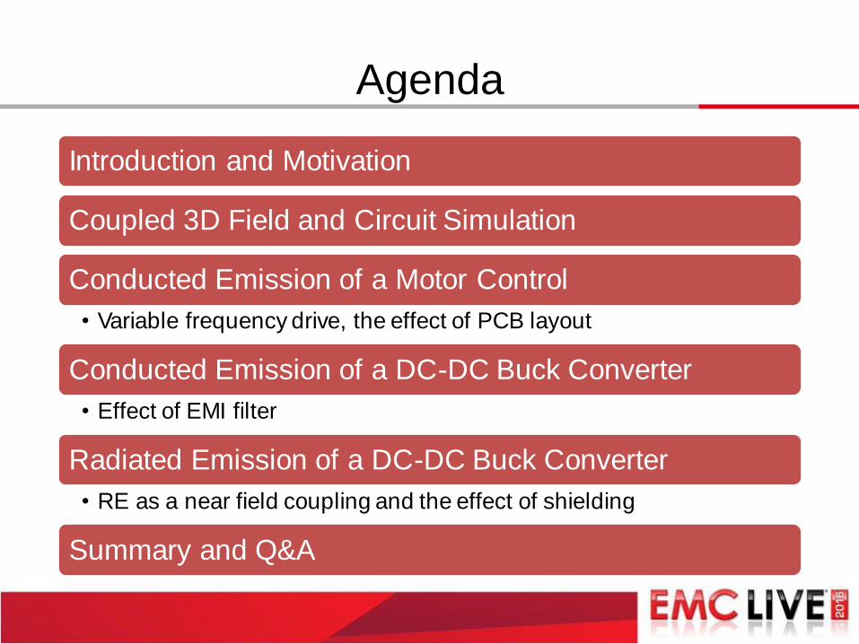
Introduction and Motivation
Coupled 3D Field and Circuit Simulation
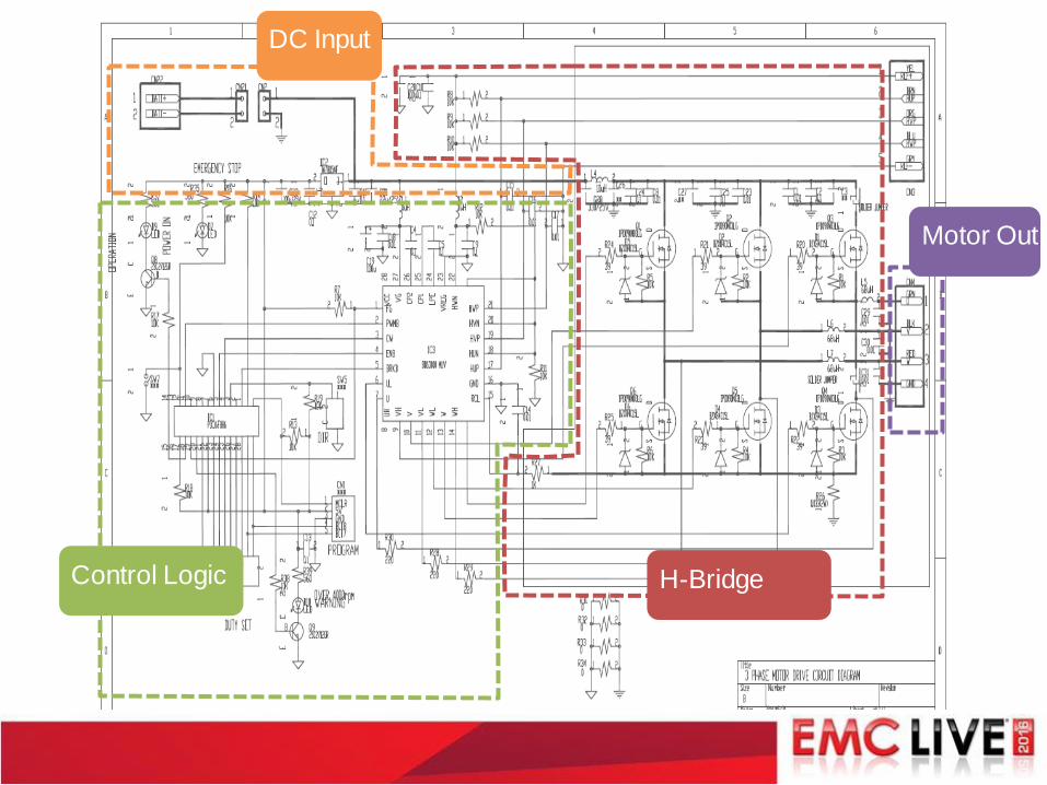
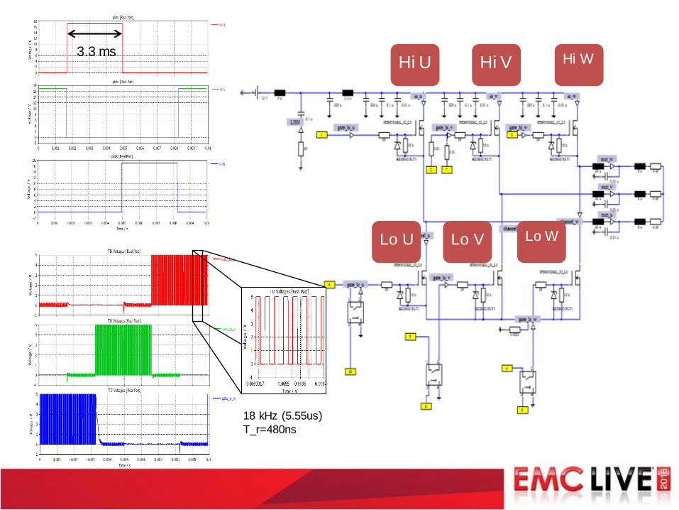
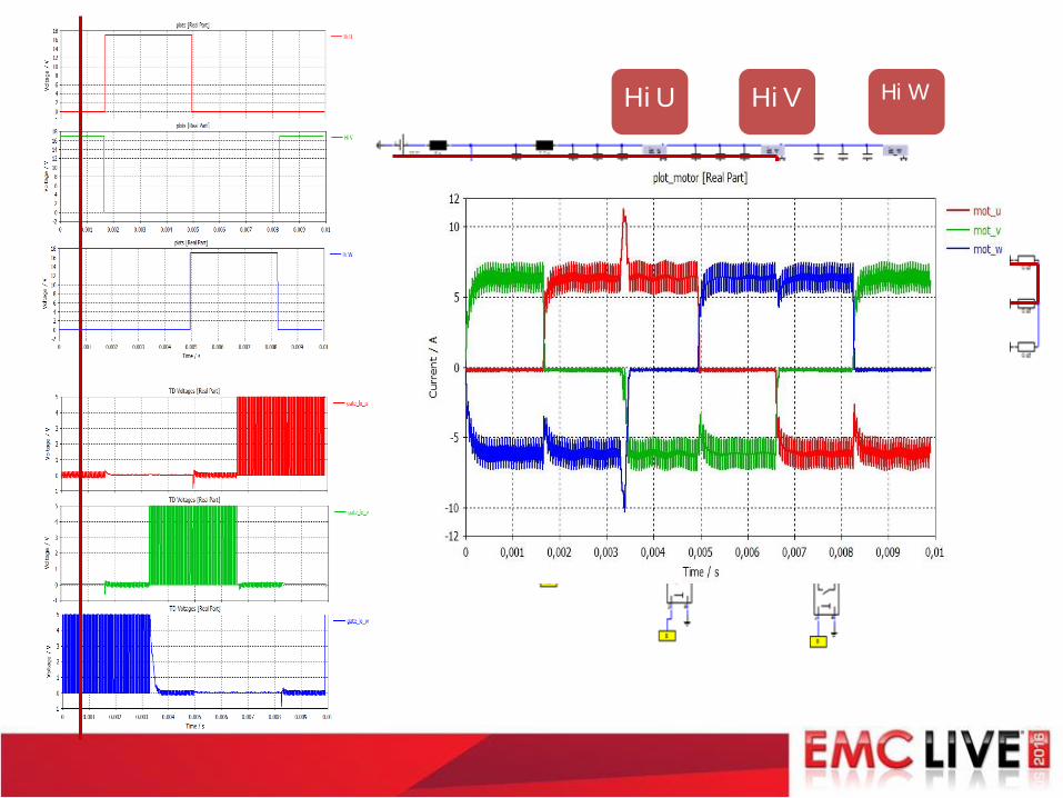
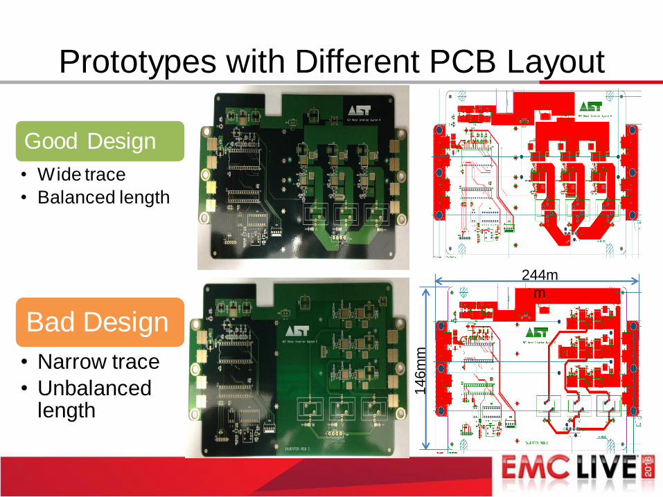
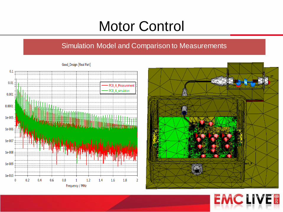
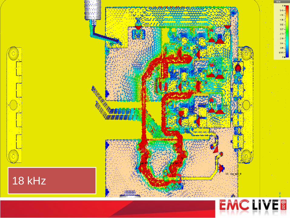
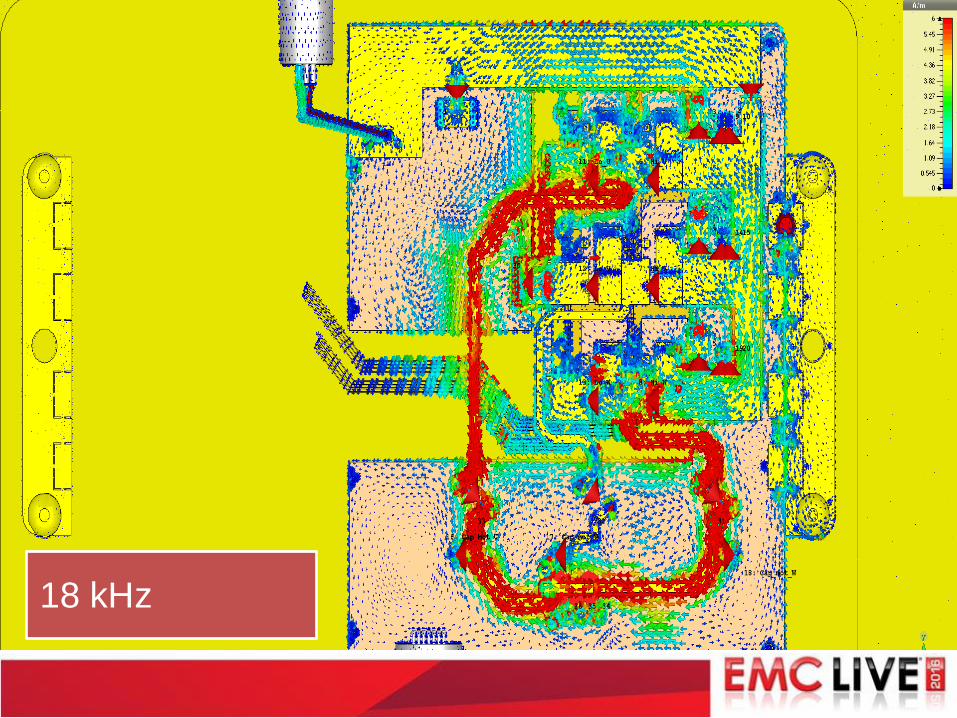
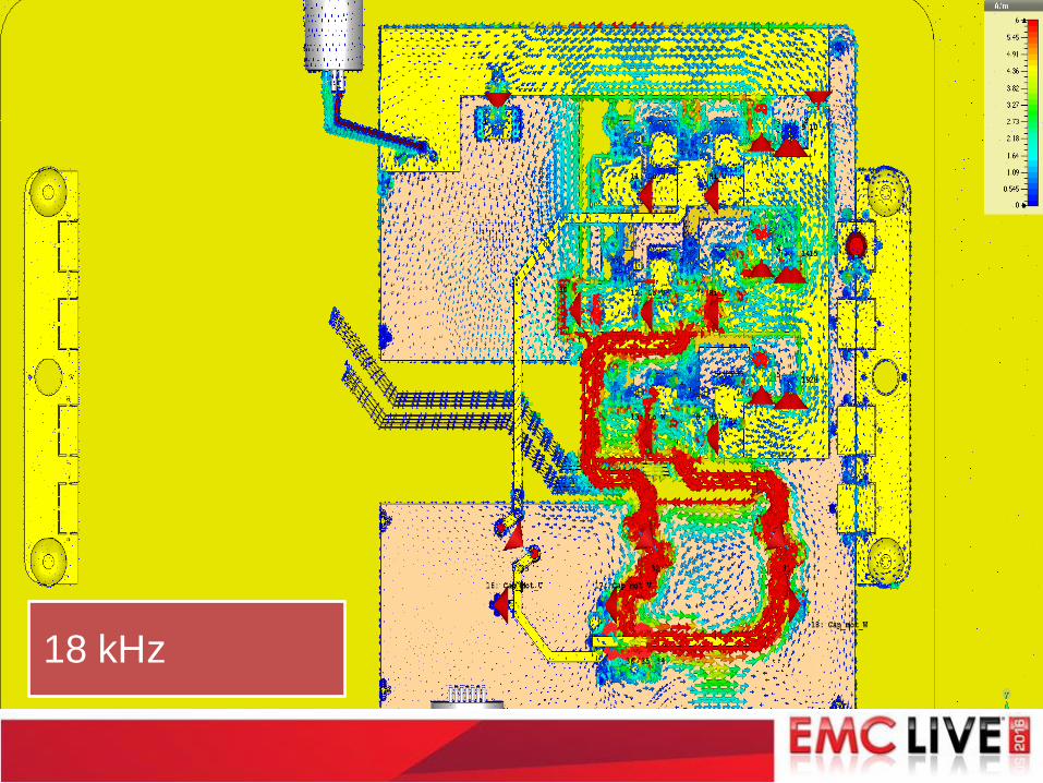
Conducted Emission of a Motor Control
• Variable frequency drive, the effect of PCB layout
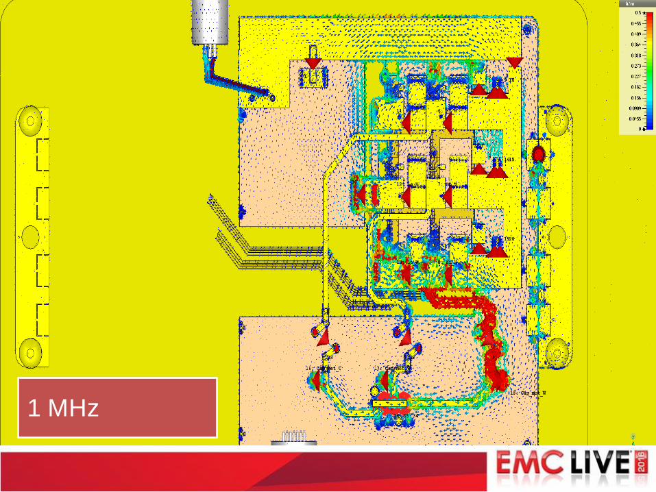
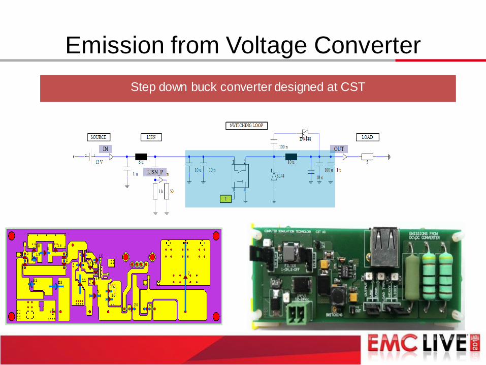
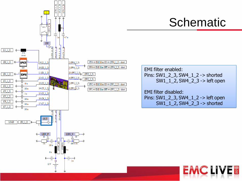
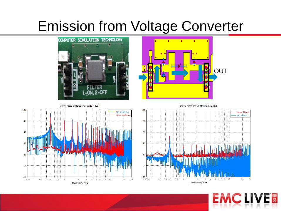
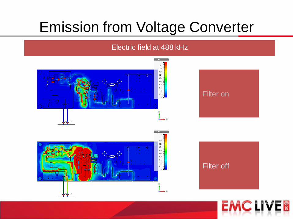
Conducted Emission of a DC-DC Buck Converter
• Effect of EMI filter
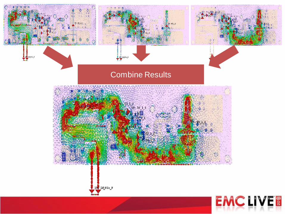
Radiated Emission of a DC-DC Buck Converter
• RE as a near field coupling and the effect of shielding
Summary and Q&A
Agenda
Introduction and Motivation
Coupled 3D Field and Circuit Simulation
Conducted Emission of a Motor Control
• Variable frequency drive, the effect of PCB layout
Conducted Emission of a DC-DC Buck Converter
• Effect of EMI filter
Radiated Emission of a DC-DC Buck Converter
• RE as a near field coupling and the effect of shielding
Summary and Q&A
Agenda
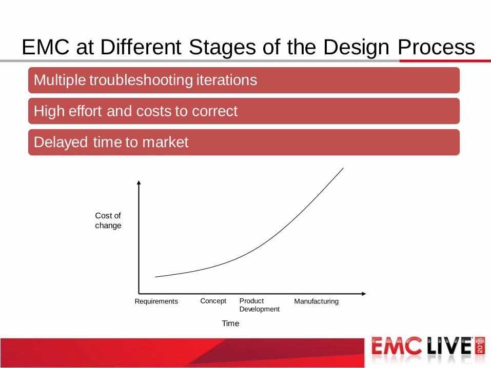
EMC at Different Stages of the Design Process
Multiple troubleshooting iterations
High effort and costs to correct
Delayed time to market
Cost of
change
Time
Requirements Concept Product Development
Manufacturing
CEM (Computational Electromagnetics) for EMC
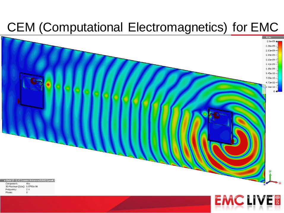
CEM (Computational Electromagnetics) for EMC
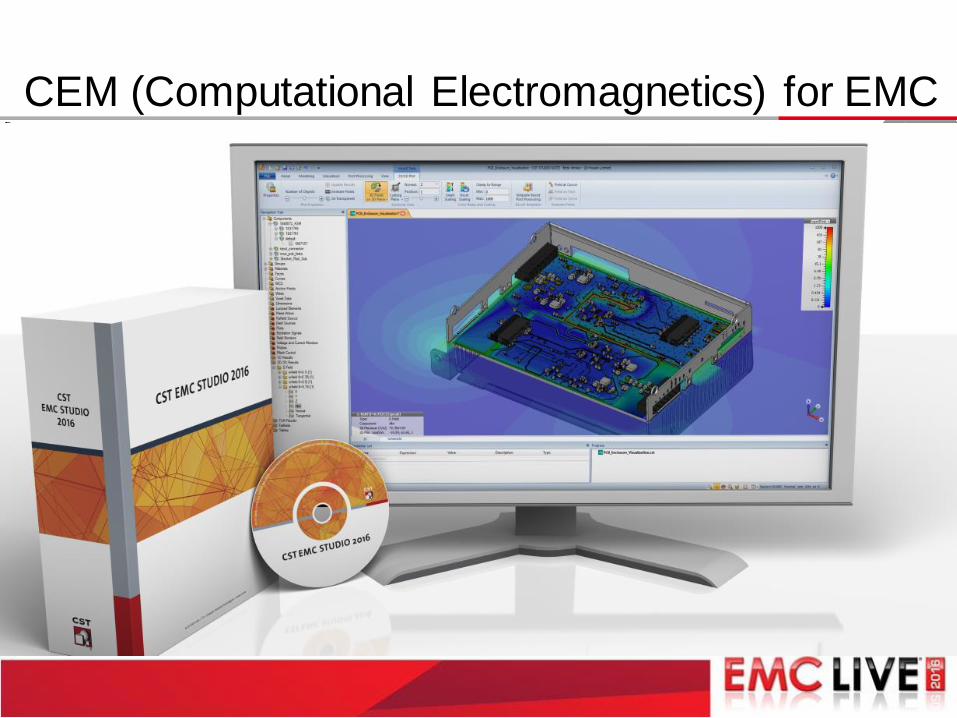
CEM (Computational Electromagnetics) for EMC
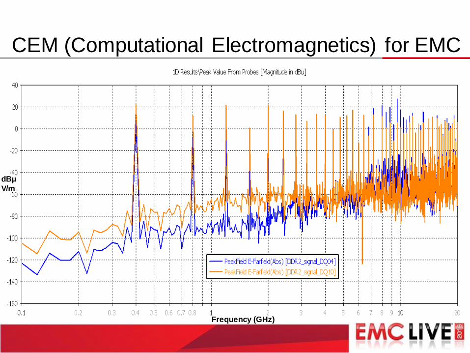
CEM (Computational Electromagnetics) for EMC
dBµ
V/m
Frequency (GHz)
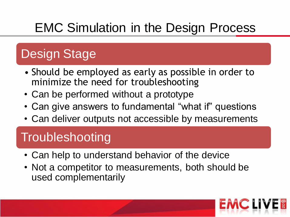
EMC Simulation in the Design Process
Design Stage
• Should be employed as early as possible in order to minimize the need for troubleshooting
• Can be performed without a prototype
• Can give answers to fundamental “what if” questions
• Can deliver outputs not accessible by measurements
Troubleshooting
• Can help to understand behavior of the device
• Not a competitor to measurements, both should be used complementarily
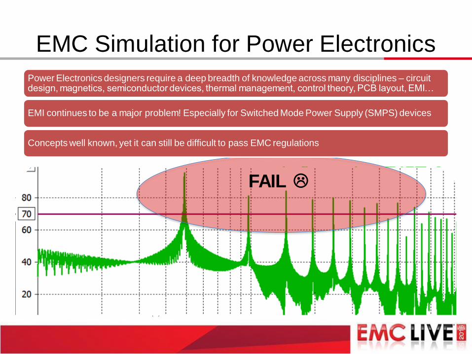
EMC Simulation for Power Electronics
FAIL
Power Electronics designers require a deep breadth of knowledge across many disciplines – circuit design, magnetics, semiconductor devices, thermal management, control theory, PCB layout, EMI…
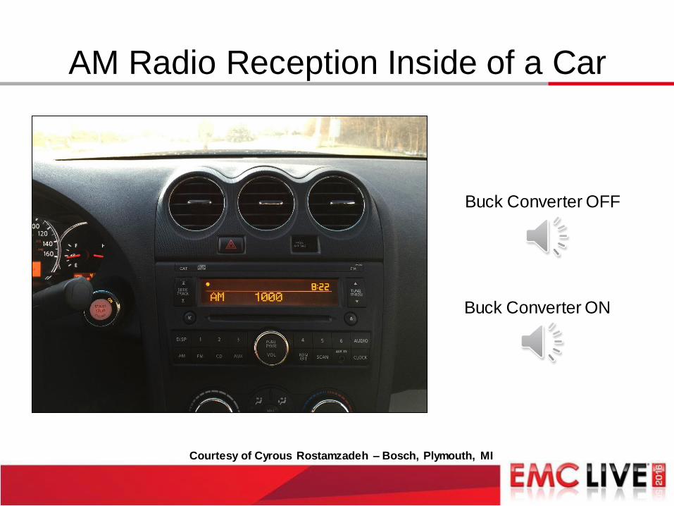
EMI continues to be a major problem! Especially for Switched Mode Power Supply (SMPS) devices
Concepts well known, yet it can still be difficult to pass EMC regulations
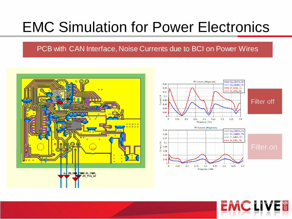
EMC Simulation for Power Electronics
Without decaps With decaps
Current distribution PCB with CAN Interface, Noise Currents due to BCI on Power Wires
Filter on
Filter off
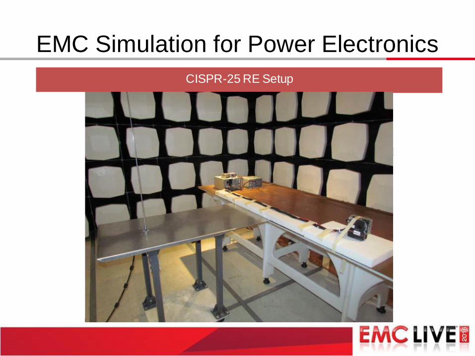
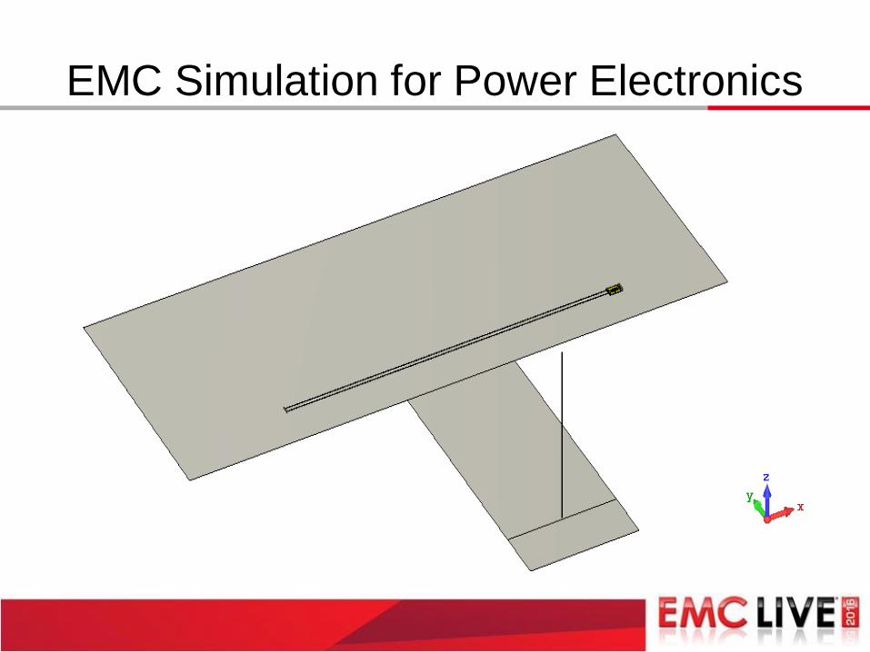
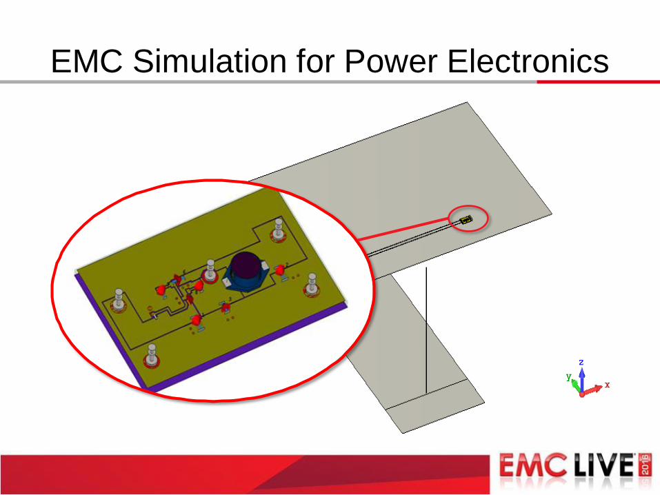
EMC Simulation for Power Electronics
CISPR-25 RE Setup
EMC Simulation for Power Electronics
EMC Simulation for Power Electronics
Introduction and Motivation
Coupled 3D Field and Circuit Simulation
Conducted Emission of a Motor Control
• Variable frequency drive, the effect of PCB layout
Conducted Emission of a DC-DC Buck Converter
• Effect of EMI filter
Radiated Emission of a DC-DC Buck Converter
• RE as a near field coupling and the effect of shielding
Summary and Q&A
Agenda
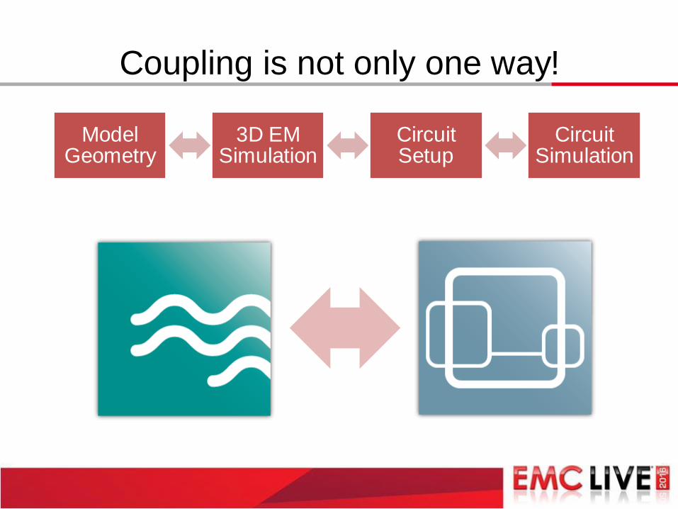
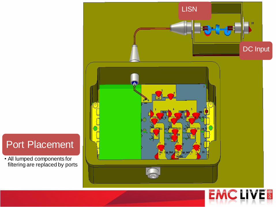
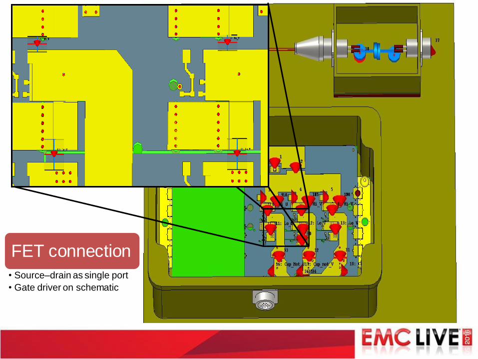
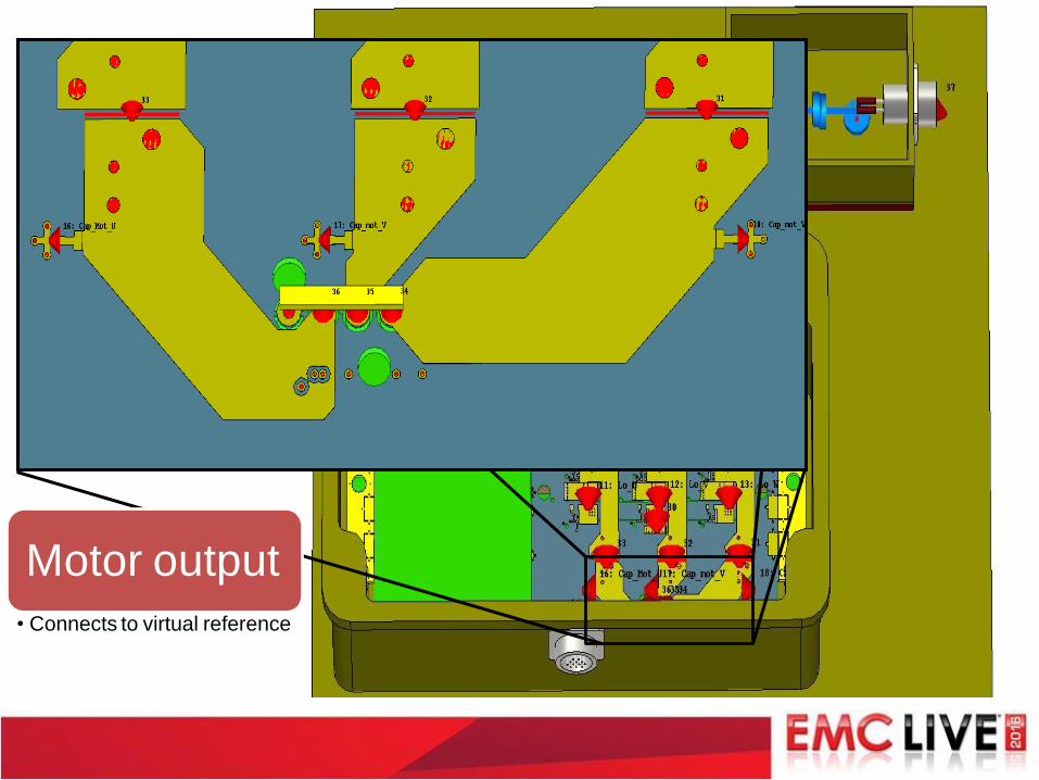
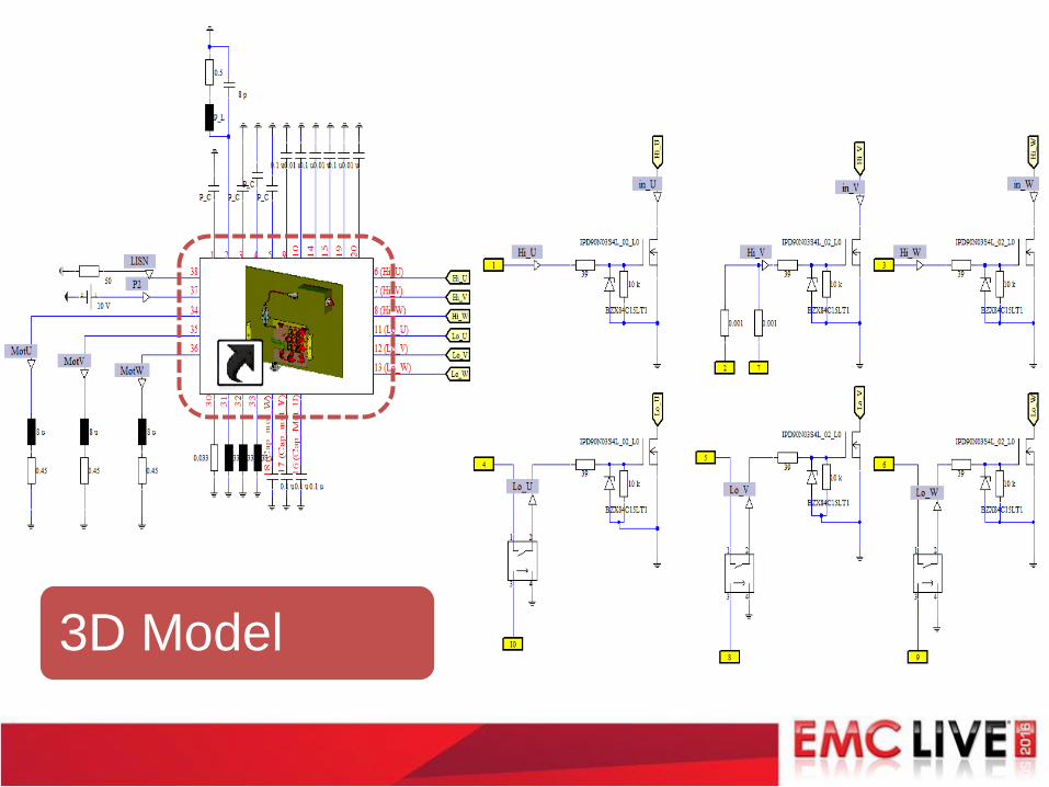
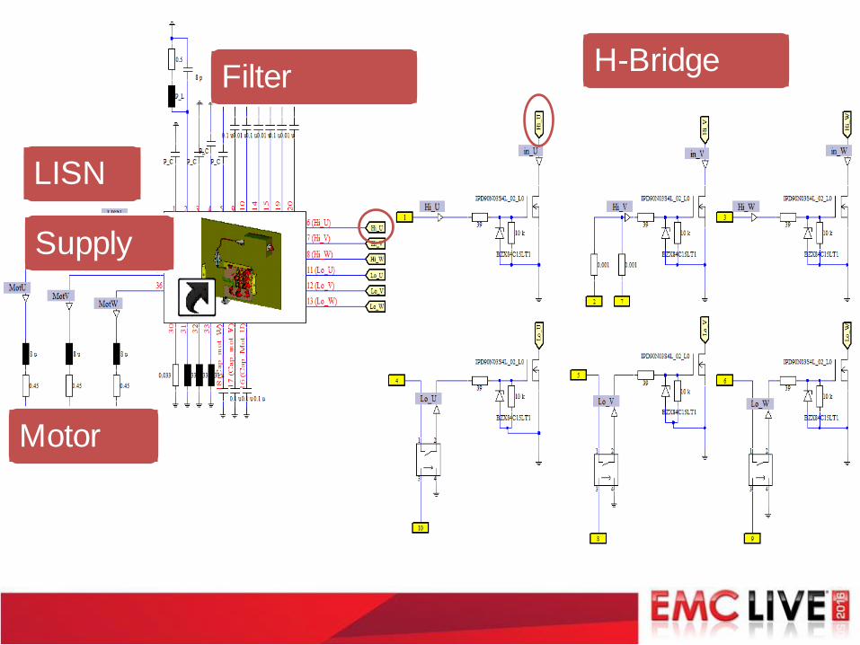
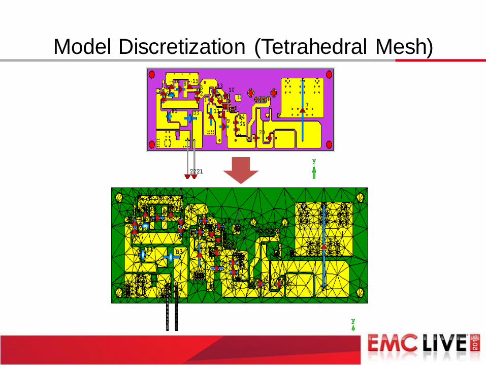
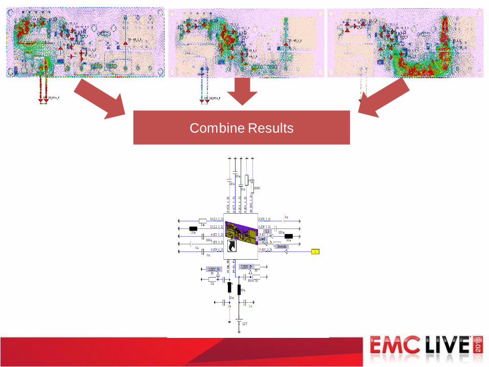
Coupled 3D Field and Circuit Simulation
Model Geometry
3D EM Simulation
Circuit Setup
Circuit Simulation
Coupling is not only one way!
Model Geometry
3D EM Simulation
Circuit Setup
Circuit Simulation
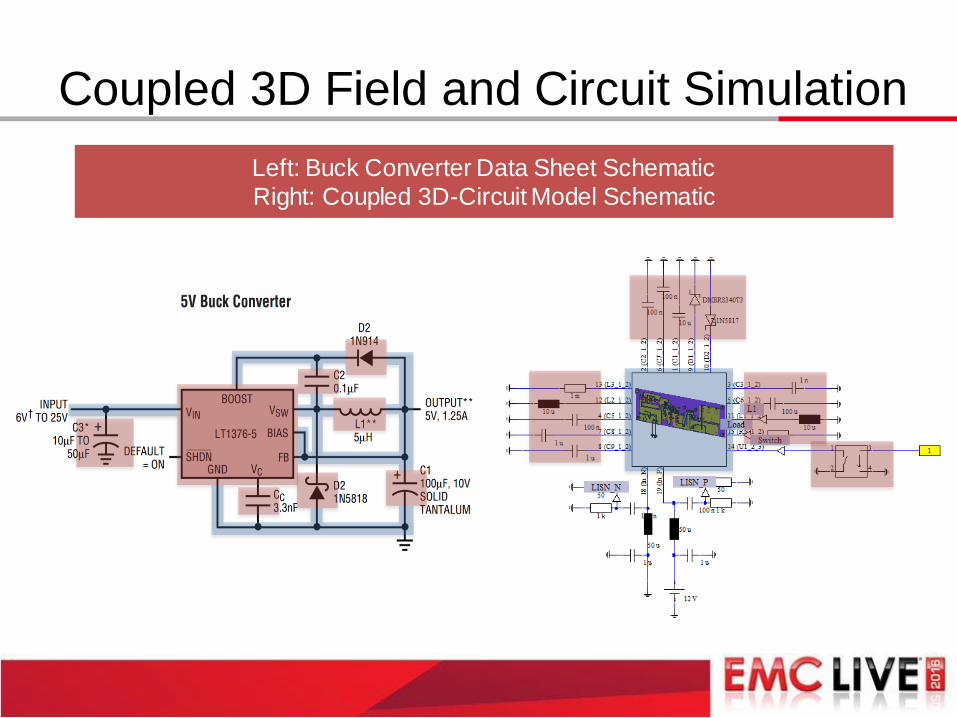
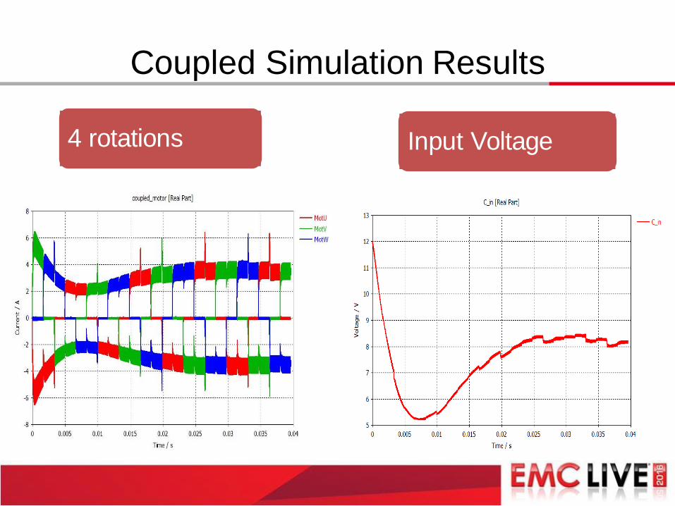
Coupled 3D Field and Circuit Simulation
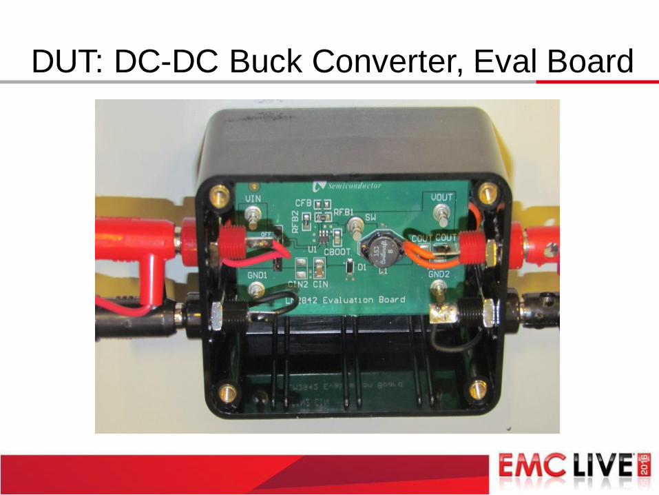
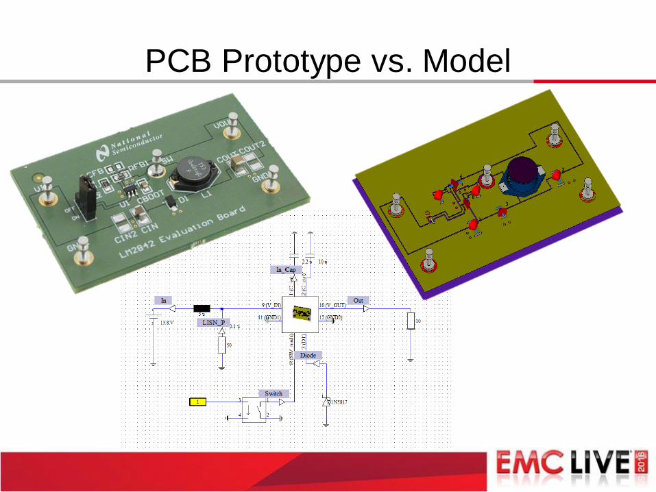
Left: Buck Converter Data Sheet Schematic
Right: Coupled 3D-Circuit Model Schematic
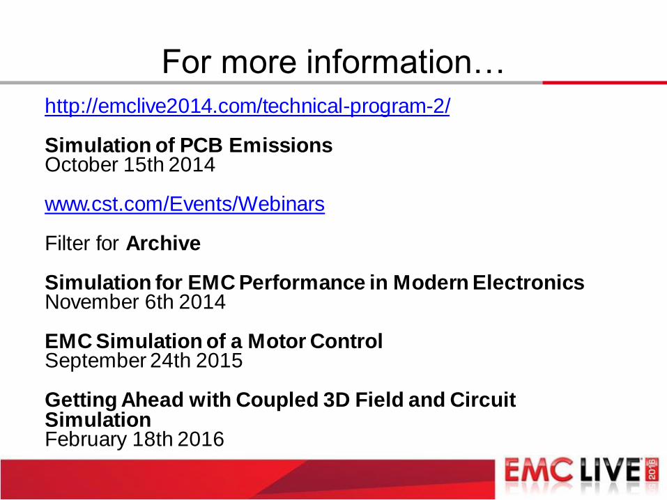
http://emclive2014.com/technical-program-2/ Simulation of PCB Emissions October 15th 2014 www.cst.com/Events/Webinars Filter for Archive Simulation for EMC Performance in Modern Electronics November 6th 2014 EMC Simulation of a Motor Control September 24th 2015 Getting Ahead with Coupled 3D Field and Circuit Simulation February 18th 2016