115
EMUL51XA–PC™ User Guide Edition 1 © ICE Technology - All rights reserved worldwide.

EMUL51XA–PC™User Guide
Edition 1
© ICE Technology - All rights reserved worldwide.
EMUL51XA–PC User GuideEMUL51XA–PC User Guide
Edition 1, February 14, 2002 © Nohau Corporation ii
Contents
About this Guide vii
Downloading EMUL51XA–PC Product Documentation vii
Overview of the EMUL51XA–PC Emulator System 1
Basic Hardware and Communication Interface 1
User Interface 1
Installing and Configuring the Communications Interface 3
Communications Interfaces 3
High-Speed Parallel Box (HSP) 3
Emulator Parallel Cable (EPC) 3
Universal Serial Bus (USB) 4
LC–ISA Plug-In Board 4
Installing the LC–ISA Board 5
Checking the I/O Address Jumpers—J1 5
Verify the Target Communication Rate—Header JP1 6
PWR Header—JP2 7
Installing the LC–ISA Plug-In Board and EPC With Windows 7
Installing the LC–ISA Plug-In Board With Windows NT 7
Installing the LC–ISA Plug-In Board With Windows 95/98 10
Installing the LC–ISA Plug-In Board With Windows 2000 11
Installing EPC With Windows NT 15
Installing EPC or USB With Windows 2000 16
Installing the EMUL–PC USB 18
Overview 18
Installing Seehau 18
Connecting the Hardware 18
Verifying Driver Installation 19
Configuring Seehau and Starting the Emulator 20

iiii EMUL51XA–PC User Guide
Installing the Pod Board 23
Overview 23
How this Chapter is Organized 23
Remove Black Conducting Foam Before Using Your Pod 23
POD–51XA–G3 / G49 / C3 24
Operating Instructions 24
Dimensions 26
Emulation Memory 26
Headers 27
Features and Limitations 32
Operating Frequency for the G3 and G49 Only 33
Operating Frequency for the C3 Only 34
Mapping Capabilities 35
POD–51XA–S3 36
Operating Instructions 36
Dimensions 38
Emulation Memory 38
Headers 39
Features and Limitations 44
Operating Frequency 46
Mapping Capabilities 47
POD–51XA–SCC 48
Operating Instructions 48
Dimensions 49
Headers 49
Features and Limitations 51
Application Notes 52
Installing and Configuring the Seehau Software 55
Installing Seehau Software from a CD 55
Downloading and Installing Seehau from the Internet 55
Selecting to Automatically Start the Seehau ConfigurationProgram 56

EMUL51XA–PC User GuideEMUL51XA–PC User Guide
Edition 1, February 14, 2002 © Nohau Corporation iiiiii
Configuring the Emulator Options 57
Connect Tab 57
Hdw Cfg Tab 58
Hdw Cfg Tab for the SCC 61
Configuring the Emulator Options From Within Seehau 62
Buttons Common to All Tabs 62
Hdw Cfg Tab 63
Hdw Cfg Tab for the SCC 65
Misc Setup Tab 67
Map Config Tab 67
Map Config Tab for the SCC 69
BP Setup Tab 70
Add Address Range Dialog Box 70
Edit Address Range Dialog Box 71
Introduction to Tracing 73
Overview 73
Normal Mode 73
Window Mode 74
Common Uses of Tracing 74
Basic Features of Tracing 75
Configuring the Trace Board 77
Trace Window 77
Trace Menu 78
Trace Configuration Window 81
Buttons Common to All Tabs 81
Trace Setup Tab 82
Trigger 1, 2 and 3 Tabs 84
Filter Tab 84
Trigger Qualifier Dialog Box 85
Data Qualifier Dialog Box 86

iviv EMUL51XA–PC User Guide
Pod Adapters 87
Overview 87
Direct Pin-to-Socket Connection 87
Solder-Down Adapter 87
C3, G3 and G49 Pod Adapters 87
Solder-Down Adapters 88
S3 Pod Adapters 90
Direct Pin-to-Socket Connections 90
SCC / H3 / H4 Pod Adapters 91
Solder-Down Adapters 92
Troubleshooting 93
Overview 93
Not Working in Stand-Alone Mode 93
Not Working With New Target System 94
Software Will Not Start Up (Fatal Error) 94
Software Starts Up, But Code Will Not Execute Properly 95
No Longer Working in Target System 95
Index 97
Sales Offices, Representatives and Distributors
EMUL51XA–PC User GuideEMUL51XA–PC User Guide
Edition 1 EMUL51XA–PC User Guide vv
Product Notes
Warranty Information
The emulator board, trace board, pod board, and emulator cable are sold with a one-year warrantystarting from the date of purchase. Defective components under warranty will either be repaired orreplaced at Nohau’s discretion.
Pod boards that use a bondout processor are also warranted for one year from the date of purchaseexcept for the processor. The bondout processor will be replaced once if Nohau determines thatthe failure in the bondout processor was not due to the user’s actions. This replacement limit doesnot apply to the rest of the pod board.
Each optional adapter, cable, and extender is sold with a 90-day warranty, except that it may besubject to repair charges if damage was caused by the user’s actions.
Nohau’s Seehau software is sold with no warranty, but upgrades can be obtained to all customersat the Nohau web site: http://www.nohau.com.
Nohau makes no other warranties, express or implied, including, but not limited to the impliedwarranties of merchantability and fitness for a particular purpose. In no event will Nohau beliable for consequential damages. Third-party software sold by Nohau carries the manufacturer’swarranty.
European CE Requirements
Nohau has included the following information in order to comply with European CE requirements.
User Responsibility
The in-circuit debugger application, as well as all other unprotected circuits need special mitiga-tion to ensure Electro Magnetic Compatibility (EMC).
The user has the responsibility to take required measures in the environment to prevent otheractivities from disturbances from the debugger application according to the user and installationmanual.
If the debugger is used in an environment other than the intended (for example, field serviceapplications), it is the user’s responsibility to control that other activities cannot be disturbed insuch a way that there may be risk for personal hazard/injuries.

vivi EMUL51XA–PC User Guide
Special Measures for Emission Requirements
To reduce the disturbances to meet conducted emission requirements it is necessary to place aground plane on the table under the pod cable and the connected processor board. The groundplane shall have a low impedance ground connection to the host computer frame. The insulationsheet between the ground plane and circuit boards shall not exceed 1mm of thickness.
System Requirements
CAUTION
Like all Windows applications, the Seehau software requires a minimum amount of free operat-
ing system resources. The recommended amount is at least 40%. Below this percentage, See-
hau might become slow, unresponsive or even unstable. If you encounter any of these
conditions, check your free resources. If they are under 40%, reboot and limit the number of con-
currently running applications. If you are unable to free more than 40% operating system re-
sources, contact your system administrator or Nohau Technical Support.
The following are minimum system requirements:
• Pentium 200 (Pentium II or faster is recommended)
• Single-Processor System
• Windows 95/98/ME, or NT/2000 PRO/XP (95 and NT do not support USB.)
• Random Access Memory (RAM)
– For Windows 95/98: 64 MB
– For Windows NT/2000/ME: 128 MB

EMUL51XA–PC User GuideEMUL51XA–PC User Guide
Edition 1 EMUL51XA–PC User Guide viivii
About this Guide
The EMUL51XA–PC User Guide describes how to use the EMUL51XA–PC emulation systemwith the Seehau graphical user interface. This book is intended for both novice and advancedusers.
Downloading EMUL51XA–PC Product Documentation
To download an electronic version of this guide, do the following:
1. Open Nohau's home page at www.nohau.com.
2. Click Publications/Documents.
3. Click Nohau Manuals.
4. Scroll down to EMUL51XA–PC. Then select EMUL51XA–PC User Guide to download aPDF version of this guide.

viiiviii EMUL51XA–PC User Guide
EMUL51XA–PC User GuideEMUL51XA–PC User Guide
Edition 1 EMUL51XA–PC User Guide 11
Overview of the EMUL51XA–PCEmulator System
Basic Hardware and Communication Interface
The EMUL51XA–PC system provides real-time emulation for both single-chip and externalmodes and includes the following:
• Communications Interface
– High-Speed Parallel (HSP) Box
– Emulator Parallel Cable (EPC).
– ISA card—requires an 8-bit ISA slot.
– Low-Cost Industry Standard Architecture (LC-ISA)
– Universal Serial Bus (USB)
• Emulator Board
• Optional Trace Board
• Adapter to connect to your target system
User Interface
The emulator is configured and operated by the Seehau user interface.
Seehau is a high-level language user interface that allows you to do many useful tasks,for example:
• Load, run, single-step and stop programs based on C or Assembly languages.
• Set triggers and view trace.
• Modify and view memory contents including SFRs.
• Set software and hardware breakpoints.

Chapter 1. Overview of the EMUL51XA–PC Emulator SystemChapter 1. Overview of the EMUL51XA–PC Emulator System
22 EMUL51XA–PC User Guide

EMUL51XA–PC User GuideEMUL51XA–PC User Guide
Edition 1 EMUL51XA–PC User Guide 33
Installing and Configuring theCommunications Interface
Communications Interfaces
To operate the EMUL51XA–PC Emulator System, you must use one of the following communi-cations interfaces to connect to an emulator board:
• High-Speed Parallel Box (HSP)—Connects to the parallel printer port. See the following“High-Speed Parallel (HSP) Box” section.
• Emulator Parallel Cable (EPC)—Communicates with the emulator system through a stan-dard PC parallel port (LPTx). See the following “Emulator Parallel Cable (EPC)” section.
• Industry Standard Architecture (ISA)—Refers to the external ISA emulator board. Thisboard is discontinued, but is still supported under Seehau. (For more information, contact No-hau Technical Support.)
• Low-Cost Industry Standard Architecture (LC-ISA)—Requires an 8-bit ISA slot. Includesa cable that connects the ISA board to the emulator board. See the following “LC-ISA Plug-InBoard” section.
• Universal Serial Bus (USB)—The USB provides one of the most portable methods of con-nection, but your ability to use this option depends upon whether your computer has a USBport and the type of operating system you are running. The USB option is not supported byWindows 95/NT and is limited to Windows operating systems 95B or later. See the following“Universal Serial Bus (USB)” section.
For detailed instructions on how to installing these devices, refer to the Windows installation in-structions later in this chapter.
High-Speed Parallel Box (HSP)
The HSP is used only with older XA systems that have an ISA emulator board and a trace board.
Emulator Parallel Cable (EPC)
The EPC allows you to connect to a standard PC parallel port and communicate with the XA podboard. Figure 1 shows both ends of the cable: the male side connects to the PC, and the femaleside connects to the printer.

Chapter 2. Installing and Configuring the Communications InterfaceChapter 2. Installing and Configuring the Communications Interface
44 EMUL51XA–PC User Guide
Figure 1. Emulator Parallel Cable
Universal Serial Bus (USB)
When using a laptop computer, the USB interface provides one of the most portable methodsof connection and allows for full trace capability. A USB port is an external peripheral interfacestandard for communication between a computer and external peripheral over a cable that usesbi-serial transmission.
You can use the USB to run the in-circuit emulator and optional trace board when ISA slots areunavailable in your computer. The USB is an interface that uses a standard USB cable to attach thePC’s USB port to the USB module that plugs into the pod board.
Note
When using the USB option, you must install the Seehau software first before
connecting the Nohau hardware. This allows the computer to recognize the proper
driver for the hardware.
The USB option is not supported by Windows 95/NT. It is anticipated that the USB
option will eventually replace the parallel port interface.
LC–ISA Plug-In Board
The EMUL/LC–ISA board is an 8-bit PC card that fits into any ISA slot (Figure 2). The jumperson the emulator board control three things: (1) the address used to communicate with the Host PC,(2) the maximum PC clock communication rate to the target, and (3) whether or not power is pro-vided to the target through the LC connector.

EMUL51XA–PC User GuideEMUL51XA–PC User Guide
Edition EMUL51XA–PC User Guide 55
JP1
NOHAU CORP.EMUL/LC-ISAS/N
A9
RP1
PW
R
A3
J1
Figure 2. LC–ISA Board
Installing the LC–ISA Board
When installing the LC–ISA Board, you will need to check the following three items:
• Check the I/O Address Jumpers.
• Verify the target communication rate.
• Check to ensure the JP2 PWR power jumper is removed.
Checking the I/O Address Jumpers—J1
Note
The factory default is set at 200 for the software and hardware. Refer to the
Windows NT and Windows 95/98 installation instructions later in this chapter to
determine if this default address will conflict with your existing PC hardware.

Chapter 2. Installing and Configuring the Communications InterfaceChapter 2. Installing and Configuring the Communications Interface
66 EMUL51XA–PC User Guide
PC Bus AddressPin Labels
Jumper Settings
200 Hex
Factory Default
A3 A9
Figure 3. Default Settings for the Emulator Header J1
PC Bus AddressPin Labels
Jumper Settings
208 Hex
Alternate Address
A3 A9
210 Hex
A3 A9
Alternate Address
PC Bus AddressPin Labels
Jumper Settings
300 Hex
A3 A9
Alternate Address
310 Hex
A3 A9
Alternate Address
Figure 4. Alternate Address Settings for the Emulator Header J1
Set the emulator board address using the jumpers in header J1. The EMUL/LC–ISA requires eightconsecutive I/O addresses from the PC’s I/O address space (0 Hex – 3FF Hex) that begin on anaddress that is a multiple of eight. These addresses must not conflict with any other I/O device.
Each pair of pins in J1 represents one bit in the 10-bit address. Address bits 0, 1, and 2 representaddresses within the eight consecutive addresses and do not have pin pairs to represent them. Thisleaves seven address bits (pin pairs) to set with jumpers. Shorting pins represents a 0 (zero)in theaddress. A pair of pins with no jumper represents a 1. Figure 4 shows four examples where theLeast Significant Bit (LSB) is on the left and the 25-pin D connector on the right.
Verify the Target Communication Rate—Header JP1
The communication clock rate is divided by moving the jumper on JP1.
Refer to Figure 5 to set the fixed synchronous communication rate. Note the clock rate in thelower row. Place one jumper on the header JP1 between the pins indicated in the upper row.Make sure only one jumper is connected to this header.

EMUL51XA–PC User GuideEMUL51XA–PC User Guide
Edition 1, EMUL51XA–PC User Guide 77
Figure 5. Default Position for Header JP1
Note
The pins on header JP1 are not numbered on the board.
Figure 5 shows the orientation of JP1 as it appears on the emulator interface board. Both pin 1holes are shown as squares as they are seen on the LC–ISA communications interface board.
Note
The default position shown in Figure 5 should work for most computer applications.
However, if you experience a communications problem, move the jumper one or
two positions to the right.
PWR Header—JP2
This jumper must be removed when the LC-ISA card is used with an EMUL51XA pod.
Installing the LC–ISA Plug-In Board and EPC WithWindows
The following describes Windows NT and Windows 95/98 installation procedures for the LC–ISAplug-in board and the EPC.
Installing the LC–ISA Plug-In Board With Windows NT
To install the LC–ISA plug-in board, you will need to check for two items:
• Check whether you have administrative privileges to install Nohau software underWindows NT.
• Check for possible conflicts with your PC and the default address range for the LC–ISA card.

Chapter 2. Installing and Configuring the Communications InterfaceChapter 2. Installing and Configuring the Communications Interface
88 EMUL51XA–PC User Guide
Checking Administrative PrivilegesChecking Administrative Privileges
To check whether you have administrative privileges, do the following:
1. Click the Start menu, and select Programs.
2. Select Administrative Tools, and click User Manager.The User Manager dialog box appears.
3. In the bottom half of the dialog box, double-click Administrators.The Local Group Properties dialog box appears with a list of login names.
4. Look for your login name in the list of names. If your login name is not present, you are not setup with administrative privileges. Contact your System Administrator to update your privi-leges or give you the administrator’s password.
Checking Your PC for Conflicts with the Default Address RangeChecking Your PC for Conflicts with the Default Address Range
The default address range for the LC–ISA card is 200H to 207H. You will need to check your PCfor possible conflicts with this default.
1. Click the Start menu, and select Programs.
2. Select Administrative Tools, and click Windows NT Diagnostics.The Windows NT Diagnostics screen appears.
3. Click the Resources tab.
4. Click the I/O Port button.
5. Check the I/O resources listed to make sure there is no device in the default address range.
If you see a device present in that range, look for an alternate address. Start at address 100H.Look for a range in multiples of eight with no device present. For example, the base addressmust be an even multiple of eight (such as 200 or 208). If you have to change the address ofthe emulator, make sure you change both the jumpers on the board and the software settings.
After installing the Seehau software and rebooting the PC, Windows NT Diagnostics will show theNohauXA device driver present in the upper I/O range (FFxx). After launching SeehauXA, thedriver is reassigned to the actual address range. In the Control Panel Devices window, you will seethree columns: Device, Status and Startup
• Device: lists the Nohau device driver
• Status: displays Started
• Startup: displays Automatic

EMUL51XA–PC User GuideEMUL51XA–PC User Guide
Edition 1, EMUL51XA–PC User Guide 99
TroubleshootingTroubleshooting
• If you get a Service or driver failed error upon reboot, you probably have a resource conflict.
• If you get a create file failed error message upon execution, the device driver did not properlystart. Review the steps in this section again. You can use Windows NT Diagnostics to re-check that your port address has no conflicts.

Chapter 2. Installing and Configuring the Communications InterfaceChapter 2. Installing and Configuring the Communications Interface
1010 EMUL51XA–PC User Guide
Installing the LC–ISA Plug-In Board With Windows 95/98
The default address range for the LC–ISA card is 200H to 207H. You will need to check your PCfor possible conflicts with this default by doing the following:
1. Click the Start menu, and select Settings.
2. Click Control Panel.
3. Double-click System.The System Properties screen appears.
4. Click the Device Manager tab.
5. Click the Properties button.
6. Click the Input/output button. Scroll the contents of the window to make sure there is nodevice in that range.
If you see a device present in the default range, look for an alternate address. Start at address100H and look for a range in multiples of eight with no device present. For example, the baseaddress must be an even multiple of eight (such as 200 or208). If you have to change theaddress of the emulator, be sure to change both the jumpers on the board and the softwaresettings.

EMUL51XA–PC User GuideEMUL51XA–PC User Guide
Edition 1, EMUL51XA–PC User Guide 1111
Installing the LC–ISA Plug-In Board With Windows 2000
To install the LC–ISA you will need to check the following items:
• Check whether you have administrative privileges to install Seehau software under Windows2000.
• Check for possible conflicts with your PC and the default address range of the LC–ISA card.
Checking Administrative PrivilegesChecking Administrative Privileges
1. Click the Start menu, select Settings, and then Control Panel.
2. Double-click the Users and Passwords icon to open the Users and Passwords window(Figure 6).
3. In the Users tab, select your user account and then click Properties to open the Propertieswindow.
4. Select the Group Memberships tab (Figure 7). If the Standard User option is not selected, orAdministrator is not listed in the Other field box, contact your systems administrator to obtainan account with proper privileges or the administrator password.
Figure 6. Users and Passwords Window Displaying the Users Tab

Chapter 2. Installing and Configuring the Communications InterfaceChapter 2. Installing and Configuring the Communications Interface
1212 EMUL51XA–PC User Guide
Figure 7. Group Membership Tab
Checking Your PC for Conflicts With the Default Address RangeChecking Your PC for Conflicts With the Default Address Range
To check your PC for possible conflicts with the default address range for the LC–ISA (200H to207H), do the following:
1. Click the Start menu, select Settings, and then Control Panel.
2. Double-click the Computer Management icon to open the Computer Management window(Figure 8).
3. Select and expand the System Information icon.
4. Select and expand the Hardware Resources folder.
5. Select the I/O folder and check for any conflicts (Figure 8).

EMUL51XA–PC User GuideEMUL51XA–PC User Guide
Edition 1, EMUL51XA–PC User Guide 1313
Figure 8. Computer Management Window With the I/O Folder Selected
If you see a device present in that range, look for an alternate address. Start at address 100H. Lookfor a range in multiples of eight with no device present. For example, the base address must bean even multiple of eight (such as 200 or 208). If you have to change the address of the LC–ISAboard, make sure you change both the jumpers on the board and the settings in your Seehau Con-figuration.
After installing the Seehau software and rebooting the PC, you can check for the device driver bydoing the following:
1. Click the Start menu, select Settings, and then Control Panel.
2. Double-click the Administrative Tools icon.
3. Double-click the Computer Management icon to open the Computer Management window(Figure 9).
4. Select and expand the System Information icon.
5. Select and expand the Software Environment folder.
6. Select the Drivers folder (Figure 9).
7. Make sure your driver is listed in the Name column and Running is indicated in the Statecolumn.

Chapter 2. Installing and Configuring the Communications InterfaceChapter 2. Installing and Configuring the Communications Interface
1414 EMUL51XA–PC User Guide
Figure 9. Computer Management Window With the Drivers Folder Selected
TroubleshootingTroubleshooting
• If you get a Service or driver failed error upon reboot, you probably have a resource conflict.
• If you get a create file failed error message upon execution of the Seehau software, the devicedriver did not properly start.

EMUL51XA–PC User GuideEMUL51XA–PC User Guide
Edition 1, EMUL51XA–PC User Guide 1515
Installing EPC With Windows NT
You must have administrative privileges and be logged on as an administrator to install Nohausoftware under Windows NT.
Checking Your PC for Conflicts With the Default Address RangeChecking Your PC for Conflicts With the Default Address Range
To check whether you have administrative privileges, do the following:
1. Click the Start menu, and select Programs.
2. Select Administrative Tools, and click User Manager.The User Manager dialog box appears.
3. In the bottom half of the dialog box, double-click Administrators.The Local Group Properties dialog box appears with a list of login names.
4. Look for your login name in the list of names. If your login name is not present, you are not setup with administrative privileges. Contact your System Administrator to update your privi-leges or give you the administrator’s password.
TroubleshootingTroubleshooting
• If you get a Service or driver failed error when rebooting, you probably have a resourceconflict.
• If you get a create file failed error message upon execution, the device driver did not properlystart.

Chapter 2. Installing and Configuring the Communications InterfaceChapter 2. Installing and Configuring the Communications Interface
1616 EMUL51XA–PC User Guide
Installing EPC or USB With Windows 2000
To install the EPC or USB you will need to check the following items:
• Check whether you have administrative privileges to install Seehau software underWindows 2000.
• Check that the parallel port is active under the Windows environment.
Checking Administrative PrivilegesChecking Administrative Privileges
1. Click the Start menu, select Settings, and then Control Panel.
2. Double-click the Users and Passwords icon to open the Users and Passwords window(Figure 10).
3. In the Users tab, select your user account and then click Properties to open the Propertieswindow.
4. Select the Group Memberships tab (Figure 11). If the Standard User option is not selected, orAdministrator is not listed in the Other field box, contact your systems administrator to obtainan account with proper privileges or the administrator password.
5. After obtaining the proper privileges, install the software and reboot the system.
6. While rebooting the system connect your communication cable to the emulator and thecomputer.
7. If you are using the USB the system will automatically install the driver for your emulator.
Figure 10. Users and Passwords Window Displaying the Users Tab

EMUL51XA–PC User GuideEMUL51XA–PC User Guide
Edition 1, EMUL51XA–PC User Guide 1717
Figure 11. Group Membership Tab
TroubleshootingTroubleshooting
• If you get a Service or driver failed error upon reboot, you probably have a resource conflict.
• If you get a create file failed error message upon execution of the Seehau software, the devicedriver did not properly start.

Chapter 2. Installing and Configuring the Communications InterfaceChapter 2. Installing and Configuring the Communications Interface
1818 EMUL51XA–PC User Guide
Installing the EMUL–PC USB
Overview
The EMUL–PC/USB is a USB communications interface used to connect the EMULXA emulatorto the host PC with a USB port.
The software must be installed before connecting the hardware or the USB driver will be present.There are four steps to install the EMUL-PC/USB:
• Installing Seehau
• Connecting the hardware
• Verifying the driver installation
• Configuring Seehau and starting the emulator
Installing Seehau
To install Seehau, do the following:
1. Place the Seehau CD into your CD-ROM drive. After Autorun executes, the Nohau SoftwareInstaller window will open.
2. Click Install Seehau Interface for EMULXA. This will start the InstallShield Wizard to guideyou through the installation process.
Connecting the Hardware
1. Check that the EPC jumper is installed. If you have previously used the EPC communications,it should already be installed.
2. Plug the female DB25 connector of the EMUL–PC/USB communication interface into theemulator interface connector as shown in Figure 12.
3. Plug the type B connector (the smaller end) of the USB cable into the EMUL–PC/USB com-munication interface.
4. Apply power to the pod.
5. Plug the type A connector (the larger end) of the USB cable into the USB port on your PC.
The operating system should detect the USB device and automatically add it to the system con-figuration.

EMUL51XA–PC User GuideEMUL51XA–PC User Guide
Edition 1, EMUL51XA–PC User Guide 1919
Figure 12. EMUL—PC/USB Connections
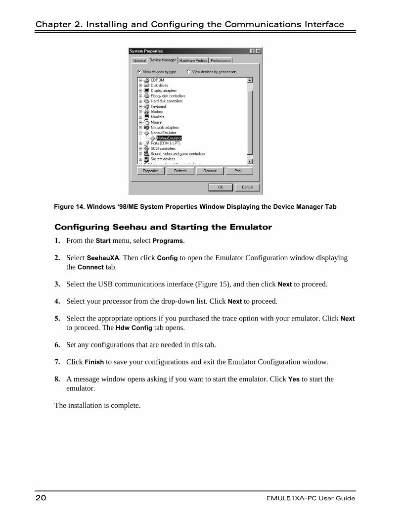
Verifying Driver Installation
For Windows 2000 PRO, XP Professional and XP Home Edition UsersFor Windows 2000 PRO, XP Professional and XP Home Edition Users
1. Right-click on the My Computer icon and select Properties.
2. Click on the Hardware tab.
3. Click Device Manager. The Device Manager window opens and Nohau Emulator is high-lighted (Figure 13).
If there is a yellow exclamation mark (!), or a red X, then you will need to reinstall the driver.
For Windows ’98 and ME UsersFor Windows ’98 and ME Users
1. Right-click on the My Computer icon and select Properties.
2. Click the Device Manager tab. The Nohau Emulator is highlighted (Figure 14).
If there is a yellow exclamation mark (!), or a red X, then you will need to reinstall the driver.
Figure 13. 2000 PRO Device Manager Window
Chapter 2. Installing and Configuring the Communications InterfaceChapter 2. Installing and Configuring the Communications Interface
2020 EMUL51XA–PC User Guide
Figure 14. Windows ‘98/ME System Properties Window Displaying the Device Manager Tab
Configuring Seehau and Starting the Emulator
1. From the Start menu, select Programs.
2. Select SeehauXA. Then click Config to open the Emulator Configuration window displayingthe Connect tab.
3. Select the USB communications interface (Figure 15), and then click Next to proceed.
4. Select your processor from the drop-down list. Click Next to proceed.
5. Select the appropriate options if you purchased the trace option with your emulator. Click Nextto proceed. The Hdw Config tab opens.
6. Set any configurations that are needed in this tab.
7. Click Finish to save your configurations and exit the Emulator Configuration window.
8. A message window opens asking if you want to start the emulator. Click Yes to start theemulator.
The installation is complete.

EMUL51XA–PC User GuideEMUL51XA–PC User Guide
Edition 1, EMUL51XA–PC User Guide 2121
Figure 15. Connect Tab Displaying USB Selected

Chapter 2. Installing and Configuring the Communications InterfaceChapter 2. Installing and Configuring the Communications Interface
2222 EMUL51XA–PC User Guide

EMUL51XA–PC User GuideEMUL51XA–PC User Guide
Edition 1, EMUL51XA–PC User Guide 2323
Installing the Pod Board
Overview
This chapter provides detailed information on four pod board types, including:
• POD–51XA–C3
• POD–51XA–G3 / G49
• POD–51XA–S3
• POD–51XA–SCC
The pod board is the main circuit board. The target adapter plugs into the bottom of the pod boardand the optional trace board plugs in between the pod board and adapter. The communications in-terface and the 5V power supply plugs into the pod board. The pod board contains the Philipsbondout microcontroller chip.
After selecting a pod type, you will need to set up the various pod board jumpers. Refer to thesection in this chapter that provides details for your pod board type including: board layoutillustrations, diagrams of jumper locations, and tables describing jumper configuration options.
How this Chapter is Organized
Pod types are listed in alphabetical order. Each pod section presents information in the followingformat:
Configuration Options: Describes configuration options.
Illustrations: Shows various configurations for switches and jumpers, target power andinternal crystal. The illustrations throughout this chapter are representative of the pod board lay-out. The notations used in the illustrations might not match the silk screens on the boards.
Special Considerations: Provides specifics about the pod’s features and functions.
Remove Black Conducting Foam Before Using Your Pod
When using your pod in stand-alone mode, be sure to remove any black conducting foam. Thisfoam is usually inserted at the factory to protect pins that mate with a target adapter or a socketon your target board. The foam covers pins which protrude from the bottom of the pod or from anadapter attached to the pod. The pod will not work with the conducting foam attached and mightcause damage.
If you remove the pod from your target socket or target adapter and plan to store it, you will needto re-install the conducting foam to protect the exposed pins.

Chapter 3. Installing the Pod BoardChapter 3. Installing the Pod Board
2424 EMUL51XA–PC User Guide
POD–51XA–G3 / G49 / C3
6.35 in.
4.
1
in
.
Adapter
Orientation(insert on bottom)
Pin 1
1 in.
2.5 cm.
1 in.
2.5 cm.
The 44-pin PGA connector
is used with a 44-pin PGA
to 44-pin PLCC adapter,
requiring one inch of
space above the target.
TOP VIEW
JP1
JP2
JP24
JP25
JP11
JP12
JP23
JP18
JP28
JP15
JP
3J
P4
JP
5J
P6
JP
7J
P8
JP
9J
P1
0
JP26
JP22
JP19
JP20
JP27
JP21
JP16JP13
J2J1
JP14
Figure 16. POD–51XA–G3 / G49 / C3
Operating Instructions
The POD–51XA–G3/G49/C3 contains a Philips bondout microcontroller chip, 256K, 1 MB or2 MB of emulation RAM, circuits for communicating with the host PC, and CPLD chips.
The pod supports 5V and low-voltage target designs down to 3.3V low-voltage target operation.You need to remove the JP15 (POD PWR) jumper and set JP16 (5V/3V) to the 3V position inorder for the pod to operate at 3.3 VDC. (The 3V position does not apply to the G49 which is a5V part.)
To work with this pod, you need to select the proper pod, memory size, and EXT or INT from theSelect Processor drop-down list in Step 3 of the Connect tab in the Emulator Configurationwindow. (To access this window, from the Start menu, select Programs, and then SeehauXA.Click on the Config icon.)
The software configurations must match the hardware jumper configurations for the data buswidthand the number of address lines. If you use a 16-bit data bus, you must have 20 bits of address.The software setup must match this setting.

EMUL51XA–PC User GuideEMUL51XA–PC User Guide
Edition 1, EMUL51XA–PC User Guide 2525
POD–51XA–G3 / G49 / C3
JP
1
JP
2
JP
24
JP
25
JP
11
JP
12
JP
23
JP
18
JP
28
JP
15
JP3 JP4 JP5 JP6 JP7 JP8 JP9 JP10
JP
26
JP
22
JP
19
JP
20
JP
27
JP
21
JP
16
JP
13
J2
J1
JP
14
NC
NC
Figure 17. Enlargement of POD–51XA–G3 / G49 / C3
Chapter 3. Installing the Pod BoardChapter 3. Installing the Pod Board
2626 EMUL51XA–PC User Guide
POD–51XA–G3 / G49 / C3
0.305 in.
7.76 mm.
0.755 in.
19.17 mm.
Adapter Disconnected
0.95 in.
24.13 mm.Adapter Connected
0.485 in.
12.32 mm.
Protector Socket
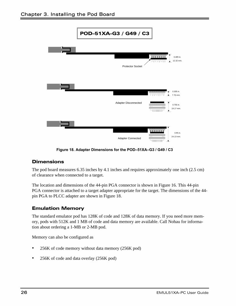
Figure 18. Adapter Dimensions for the POD–51XA–G3 / G49 / C3
Dimensions
The pod board measures 6.35 inches by 4.1 inches and requires approximately one inch (2.5 cm)of clearance when connected to a target.
The location and dimensions of the 44-pin PGA connector is shown in Figure 16. This 44-pinPGA connector is attached to a target adapter appropriate for the target. The dimensions of the 44-pin PGA to PLCC adapter are shown in Figure 18.
Emulation Memory
The standard emulator pod has 128K of code and 128K of data memory. If you need more mem-ory, pods with 512K and 1 MB of code and data memory are available. Call Nohau for informa-tion about ordering a 1-MB or 2-MB pod.
Memory can also be configured as
• 256K of code memory without data memory (256K pod)
• 256K of code and data overlay (256K pod)

EMUL51XA–PC User GuideEMUL51XA–PC User Guide
Edition 1, EMUL51XA–PC User Guide 2727
POD–51XA–G3 / G49 / C3
• 512K of code and 512K of data memory
• 1 MB of code without data memory (1-MB pod)
• 1 MB of code and data overlay (1-MB pod)
See the “Code Header—JP26 and Overlay #Header—JP22” section for details on the jumpersettings.
Headers
Figure 17 shows the headers with their jumpers in the default positions. When shipped from thefactory, all jumpers are in place for stand-alone operation (without a target). This stand-aloneoperation runs code from external code memory after reset, 20 bits of address, and 16 bits of data.
When you connect this pod to a target, be sure to examine all the jumpers for correct placement.The following sections describe the correct placement for these jumpers.
Clock HeadersClock Headers—JP1 and JP2—JP1 and JP2
These two headers each have two jumper positions: TARGET and POD. They must be moved asa pair. With both headers set in the TARGET position, the on-pod XA bondout chip receives theclock signal from the target crystal or oscillator. When using an oscillator, it is important to use a50 percent duty-cycle oscillator. With both headers set in the POD position, the XA bondout chipuses the oscillator on the pod.
Note
The XTAL1 and XTAL2 signals from the pod are disconnected from the target when
the clock jumpers are in the pod position.
EXT Mode HeaderEXT Mode Header—JP20—JP20
If you operate the XA in Internal mode (Figure 19) then you need to remove JP20. If you operatethe XA in External mode (Figure 20) then you need to install JP20.

Chapter 3. Installing the Pod BoardChapter 3. Installing the Pod Board
2828 EMUL51XA–PC User Guide
POD–51XA–G3 / G49 / C3
Figure 19. Selecting the Internal Mode Operation
Figure 20. Selecting the External Mode Operation
PC–PWR HeaderPC–PWR Header—JP14—JP14
If you run the pod with the EPC/USB interface, install JP14 and use the external power supply.When using the LC–ISA, we recommend using the external power supply and removing JP14. Torun the pod with PC power, install JP14 (the external power supply is not used).

EMUL51XA–PC User GuideEMUL51XA–PC User Guide
Edition 1, EMUL51XA–PC User Guide 2929
POD–51XA–G3 / G49 / C3
POD–PWR HeaderPOD–PWR Header—JP15—JP15
Remove JP15 if you are using power from the target for the CPU. If JP15 is not removed in thiscircumstance, the target VCC is connected to 5 V from the pod. If the target requires less than 0.5amps current, the pod can be used to power the target with JP15 installed. Higher currents cause asignificant voltage drop along the current path. This drop in voltage can damage the pod. Youneed to remove JP15 in order for the pod to operate at 3.3 VDC supplied by the target.
Target On HeaderTarget On Header—JP28—JP28
If you connect the pod to a target that could be affected by the pod outputting 1.8 volts atthe XA VCC pin and the I/O pins, remove JP28 before applying power to the target. ReinstallJP28 after applying power to the target. Similarly, remove JP28 before you turn off the targetpower. JP28 has this off-and-on capability to avoid voltage problems. By removing JP28, all thepins of the XA are tristated. However, after applying power to the target, you must reinstall JP28.
WARNING
Always turn on the PC before applying power to the target. Always turn off the target power before
turning off the PC power.
5V and 3V Header5V and 3V Header—JP16—JP16
If you operate the XA at 5V, set JP16 at the 5V position. If you operate the XA at 3.3V, set JP16 atthe 3V position.
RXD HeadersRXD Headers—JP11 and JP12—JP11 and JP12
If your target outputs debugging information on the serial port, you might want to connect anRS232 device (a terminal or a PC). This pod includes a MAX232 chip that converts the signal lev-els from RS232 to TTL levels. If you place a jumper on either RXD header, the MAX232 chipdrives the serial port input pin on the XA bondout chip. To keep the MAX232 chip from drivingthe serial input pin on the XA bondout chip, remove the jumper on the RXD header.
RS232 HeadersRS232 Headers—J1 and J2—J1 and J2
Header J1 connects to serial port 0. Header J2 connects to serial port 1.
Trace HeaderTrace Header—JP13—JP13
With the optional trace, these eight pins monitor any eight logic signals on your target board. TheTrace menu displays these pins as TR0 – TR7. TR0 is closest to the JP13 label and TR7 is closestto the 5 V/3 V jumper, JP16. (This applies to the IETR trace only. It doesn’t apply to the NIETR.)

Chapter 3. Installing the Pod BoardChapter 3. Installing the Pod Board
3030 EMUL51XA–PC User Guide
POD–51XA–G3 / G49 / C3
Reset HeaderReset Header—JP18—JP18
Occasionally, a target contains an external device designed to reset the XA chip by pulling theRST pin low. During debugging, this reset might be inconvenient. The signal from the target RSTpin passes through the RST jumper. Removing the RST jumper prevents the external device fromresetting the XA bondout chip.
Note
This is in one direction only. The target can reset the emulator if the RST jumper
is installed. The emulator will not reset the target even though the RST jumper is
installed.
TARGET / POD Wait HeaderTARGET / POD Wait Header—JP23—JP23
This header has two jumper positions: Pod and Target. When the pod operates in stand-alonemode (without a target), set JP23 in the Pod position. The pod provides the WAIT signal to the on-pod XA bondout chip. When the pod operates with a target, setting JP23 in the TARGET positionconnects the XA to the target WAIT signal. The target WAIT signal passes through JP23.
I/O Port HeaderI/O Port Header—JP19—JP19
JP19 enables the pod to recognize the signals on P3.6 and P3.7 as I/O signals, instead of WR andRD signals. Install JP19 if the XA operates in internal mode, and uses all pins on P0, P1, P2 andP3 as I/O. If the XA does not operate in internal mode, remove JP19.
Target BW HeaderTarget BW Header—JP21 and 8-Bit Header—JP27—JP21 and 8-Bit Header—JP27
The Target BW jumper, JP21, must be removed.
The 8-bit jumper, JP27, enables the on-pod XA bondout chip to run with an 8-bit wide data bus.Removing JP27 enables the on-pod XA bondout chip to run with a 16-bit wide data bus. The 8-bitjumper does not support the C3 chip.
Note
This pod does not support user programs that can override the bus width setting by
writing to the Bus Configuration Register (BCR). The bus width is determined by the
value of the BUSW pin when Reset is released.

EMUL51XA–PC User GuideEMUL51XA–PC User Guide
Edition 1, EMUL51XA–PC User Guide 3131
POD–51XA–G3 / G49 / C3
Code HeaderCode Header—JP26 and Overlay—JP26 and Overlay #Header—JP22 #Header—JP22
Table 1. Jumper Settings for the 256K Pod
256K Pod Code Header—JP26 Overlay #Header—JP22
128K code, 128K data Off On
256K code, 0K data On On
256K code, 256K data overlay Off Off
Table 2. Jumper Settings for the 1-MB Pod
1-MB Pod Code Header—JP26 Overlay #Header—JP22
512K code, 512K data Off On
1 MB code, 0 MB data On On
1 MB code, 1 MB data overlay Off Off
Table 3. Jumper Settings for the 2-MB Pod
2-MB Pod Code Header—JP26 Overlay #Header—JP22
1 MB code, 1 MB data Off Off
12 / 16-Bit and 12-Bit Headers12 / 16-Bit and 12-Bit Headers—JP24 and JP25—JP24 and JP25
JP24 and JP25 determine the number of address lines that are used by the on-pod XA bondoutchip.
Table 4. JP24 and JP25 Settings
JP 24 (12-/16-Bit) JP 25 (12-Bit) Number of Address Lines
On On 12
On Off 16
Off Off 20
Note
This pod does not support user Programs that override the number of address lines
setting by writing to the Bus Configuration Register (BCR).

Chapter 3. Installing the Pod BoardChapter 3. Installing the Pod Board
3232 EMUL51XA–PC User Guide
POD–51XA–G3 / G49 / C3
A12 – A19 HeadersA12 – A19 Headers—JP3 – JP10—JP3 – JP10
The A12 – A19 headers each have two positions: P2.x and GND. Set these headers according tothe number of address lines that were set by the JP24 and JP 25 jumpers (see Table 5).
Table 5. A12 – A19 Headers—JP3 – JP10 Settings
Number of Address Lines A12 A13 A14 A15 A16 A17 A18 A19
12 GND GND GND GND GND GND GND GND
16 P2.0 P2.1 P2.2 P2.3 GND GND GND GND
20 P2.0 P2.1 P2.2 P2.3 P2.4 P2.5 P2.6 P2.7
Features and Limitations
The emulator uses six bytes of stack space in a large memory model and four bytes of stack spacein a small memory model. You need to add six (or four) bytes to your stack size calculation toavoid a stack overflow exception at 0080H.
Emulation MemoryEmulation Memory
One of the following for the 256K pod
• 128K code and 128K data memory
• 256K code and 0K data memory
• 256K code and 256K data memory overlay
One of the following for the 1-MB pod
• 512K code and 512K data memory
• 1 MB code and 0 MB data memory
• 1 MB code and 1 MB data memory overlay
The 2-MB pod has 1 MB of code and 1 MB of data memory.
Software BreakpointsSoftware Breakpoints
You can set software breakpoints wherever there is emulation code memory.

EMUL51XA–PC User GuideEMUL51XA–PC User Guide
Edition 1, EMUL51XA–PC User Guide 3333
POD–51XA–G3 / G49 / C3
Hardware BreakpointsHardware Breakpoints
• All code address, one instruction skid
– 256K pod—256K hardware breakpoints
– 1-MB pod—1 MB hardware breakpoints
– 2-MB pod—1 MB hardware breakpoints
Fast Break WriteFast Break Write
Fast Break Write is available when the pod is operating in the external or internal mode.
Data / Address Bus ConfigurationsData / Address Bus Configurations
The configurations of an 8-bit data bus and a 12-bit address bus in external mode are notsupported.
Operating Frequency for the G3 and G49 Only
1 MHz to 25 MHz in 16-Bit Mode1 MHz to 25 MHz in 16-Bit Mode
WM0 must equal 1 in BTRL. Table 6 shows the external bus signal timing configurations.
Table 6. Configurations for 1 MHz to 25 MHz in 16-Bit Mode
CR1, CR0 CRA1, CRA0 DW1, DW0 DWA1, DWA0 DR1, DR0 DRA1,DRA0
00 Supported Supported N/A Not supported N/A Supported
01 Supported Supported N/A Supported N/A Supported
10 Supported Supported N/A Supported N/A Supported
11 Supported Supported N/A Supported N/A Supported
25 MHz to 30 MHz in 16-Bit Mode25 MHz to 30 MHz in 16-Bit Mode
WM0 must equal 1 in BTRL. Table 7 shows the external bus signal timing configurations.
Table 7. Configurations for 25 MHz to 30 MHz in 16-Bit Mode
CR1, CR0 CRA1, CRA0 DW1, DW0 DWA1, DWA0 DR1, DR0 DRA1,DRA0
00 Notsupported
Not supported N/A Not supported N/A Notsupported
01 Supported Supported N/A Supported N/A Supported
10 Supported Supported N/A Supported N/A Supported
11 Supported Supported N/A Supported N/A Supported

Chapter 3. Installing the Pod BoardChapter 3. Installing the Pod Board
3434 EMUL51XA–PC User Guide
POD–51XA–G3 / G49 / C3
1 MHz to 20 MHz in 8-Bit Mode1 MHz to 20 MHz in 8-Bit Mode
WM0 must equal 1 in BTRL. Table 8 shows the external bus signal timing configurations.
Table 8. Configurations for 1 MHz to 20 MHz in 8-Bit Mode
CR1, CR0 CRA1,CRA0
DW1, DW0 DWA1, DWA0 DR1, DR0 DRA1,DRA0
00 Supported Supported Not supported Not supported Supported Supported
01 Supported Supported Supported Supported Supported Supported
10 Supported Supported Supported Supported Supported Supported
11 Supported Supported Supported Supported Supported Supported
20 MHz to 30 MHz in 8-Bit Mode20 MHz to 30 MHz in 8-Bit Mode
WM0 must equal 1 in BTRL. Table 9 shows the external bus signal timing configurations.
Table 9. Configurations for 20 MHz to 30 MHz in 8-Bit Mode
CR1, CR0 CRA1, CRA0 DW1, DW0 DWA1,DWA0
DR1, DR0 DRA1,DRA0
00 Not supported Not supported Not supported Notsupported
Notsupported
Notsupported
01 Supported Supported Supported Supported Supported Supported
10 Supported Supported Supported Supported Supported Supported
11 Supported Supported Supported Supported Supported Supported
Operating Frequency for the C3 Only
1 MHz to 25 MHz in 16-Bit Mode1 MHz to 25 MHz in 16-Bit Mode
WM0 must equal 1 in MIFBTRL. Table 10 shows the external bus signal timing configurations.
Table 10. Configurations for 1 MHz to 25 MHz in 16-Bit Mode
CR1, CR0 CRA1, CRA0 DW1, DW0 DWA1, DWA0 DR1, DR0 DRA1,DRA0
00 Supported Supported N/A Not supported N/A Supported
01 Supported Supported N/A Supported N/A Supported
10 Supported Supported N/A Supported N/A Supported
11 Supported Supported N/A Supported N/A Supported

EMUL51XA–PC User GuideEMUL51XA–PC User Guide
Edition 1, EMUL51XA–PC User Guide 3535
POD–51XA–G3 / G49 / C3
25 MHz to 30 MHz in 16-Bit Mode25 MHz to 30 MHz in 16-Bit Mode
WM0 must equal 1 in MIFBTRL. Table 11 shows the external bus signal timing configurations.
Table 11. Configurations for 25 MHz to 30 MHz in 16-Bit Mode
CR1, CR0 CRA1, CRA0 DW1, DW0 DWA1, DWA0 DR1, DR0 DRA1,DRA0
00 Notsupported
Not supported N/A Not supported N/A Notsupported
01 Supported Supported N/A Supported N/A Supported
10 Supported Supported N/A Supported N/A Supported
11 Supported Supported N/A Supported N/A Supported
Mapping Capabilities
The mapping capabilities map code and data with 16 bytes of resolution. The mapping capabilitycovers the entire address range of the POD–51XA–G3/G49/C3 (1 MB).

Chapter 3. Installing the Pod BoardChapter 3. Installing the Pod Board
3636 EMUL51XA–PC User Guide
POD–51XA–S3
0.70 in.
2.35 in.
6.35 in.
2.
92
5
in
.
1.
12
5
in
.
4.
1
in
.
Front
Pin 1
Adapter Orientation
(insert on bottom)
1.75 in.
1.745 in.
72-Pin Connector
Location ofthe 72-PinConnector
Figure 21. POD–51XA–S3
Operating Instructions
The POD–51XA–S3 contains a Philips P51XAS3 bondout microcontroller chip, 256K, 1 MB or2 MB of emulation RAM, circuits for communicating with the host PC, and CPLD chips.
The pod supports 5V and low-voltage target designs down to 3.3V low-voltage target operation.You need to remove the JP15 (POD PWR) jumper and set JP16 (5V/3V) to the 3V position inorder for the pod to operate at 3.3 VDC.
To work with this pod, you need to select POD–51XAS3–256,1M, or 2M/IE (EXT or INT) from theSelect Processor drop-down list in Step 3 of the Connect tab in the Emulator Configurationwindow.
The software configurations must match the hardware jumper configurations for the data buswidthand the number of address lines.

EMUL51XA–PC User GuideEMUL51XA–PC User Guide
Edition 1, EMUL51XA–PC User Guide 3737
POD–51XA–S3
Figure 22. Enlargement of POD–51XA–S3

Chapter 3. Installing the Pod BoardChapter 3. Installing the Pod Board
3838 EMUL51XA–PC User Guide
POD–51XA–S3
0.755 in.
19.17 mm.
Adapter Disconnected
0.305 in.
7.76 mm.
0.755 in.
19.17 mm.
Adapter Connected
Figure 23. Adapter Dimensions for the POD–51XA–S3
Dimensions
The pod board measures 6.35 inches by 4.1 inches and requires approximately one inch (2.5 cm)of clearance when connected to a target.
The location and dimensions of the 68-pin PLCC adapter (ET/AP4-68-SUB1) is shown in Figure21. This 68-pin PLCC adapter is attached to a 72-pin connector on the bottom of the pod board.The location of the 72-pin connector is shown in Figure 21. The dimensions of the 68-pin PLCCadapter are shown in Figure 23.
Emulation Memory
The microcontroller directly addresses 128K of code and 128K of data memory. If you need morememory, pods with 1 MB and 2 MB of emulation memory are available. Call Nohau for informa-tion about ordering a 1-MB or 2-MB pod.
Memory can also be configured as
• 256K of code memory without data memory (256K pod)
• 256K of code and data overlay (256K pod)
• 512K of code and 512K of data memory
• 1 MB of code without data memory (1-MB pod)

EMUL51XA–PC User GuideEMUL51XA–PC User Guide
Edition 1, EMUL51XA–PC User Guide 3939
POD–51XA–S3
• 1 MB of code and data overlay (1-MB pod)
• 2 MB of code without data memory (2-MB pod)
• 2 MB of code and data overlay (2-MB pod)
See the “Code Header—JP26 and Overlay #Header—JP22” section for details on the jumpersettings.
Headers
Figure 22 shows the headers with their jumpers in the default positions. When shipped from thefactory, all jumpers are in place for stand-alone operation (without a target). This stand-aloneoperation runs code from external code memory after reset, 24 bits of address, and 16 bits of data.
When you connect this pod to a target, be sure to examine all the jumpers for correct placement.The following sections describe the correct placement for these jumpers.
Clock HeadersClock Headers—JP1 and JP2—JP1 and JP2
These two headers each have two jumper positions: TARGET and POD. They must be moved asa pair. With both headers set in the TARGET position, the on-pod XA bondout chip receives theclock signal from the target crystal or oscillator. When using an oscillator, it is important to use a50 percent duty-cycle oscillator. With both headers set in the POD position, the XA bondout chipuses the oscillator on the pod.
Note
The XTAL1 and XTAL2 signals from the pod are disconnected from the target when
the clock jumpers are in the POD position.
EXT Mode HeaderEXT Mode Header—JP20—JP20
If you operate the XA in Internal mode (Figure 24) then you need to remove JP20. If you operatethe XA in External mode (Figure 25) then you need to install JP20.

Chapter 3. Installing the Pod BoardChapter 3. Installing the Pod Board
4040 EMUL51XA–PC User Guide
POD–51XA–S3
Figure 24. Selecting the Internal Mode Operation
Figure 25. Selecting the External mode Operation
PC–PWR HeaderPC–PWR Header—JP14—JP14
If you run the pod with the EPC/USB interface, install JP14 and use the external power supply.When using the LC–ISA, we recommend using the external power supply and removing JP14. Torun the pod with PC power, install JP14 (the external power supply is not used).

EMUL51XA–PC User GuideEMUL51XA–PC User Guide
Edition 1, EMUL51XA–PC User Guide 4141
POD–51XA–S3
POD–PWR HeaderPOD–PWR Header—JP15—JP15
Remove JP15 if you are using power from the target for the CPU. If JP15 is not removed in thiscircumstance, the target VCC is connected to 5 V from the pod. If the target requires less than 0.5amps current, the pod can be used to power the target with JP15 installed. Higher currents cause asignificant voltage drop along the current path. This drop in voltage can damage the pod. Youneed to remove JP15 in order for the pod to operate at 3.3 VDC supplied by the target.
Target On HeaderTarget On Header—JP28—JP28
If you connect the pod to a target that could be affected by the pod outputting 1.8 volts at the XAVCC pin and the I/O pins, remove JP28 before applying power to the target. Reinstall JP28 afterapplying power to the target. Similarly, remove JP28 before you turn off the target power. JP28has this off-and-on capability to avoid voltage problems. By removing JP28, all the pins of the XAare tristated. However, after applying power to the target, you must reinstall JP28.
WARNING
Always turn on the PC before applying power to the target. Always turn off the target power before
turning off the PC power.
5V and 3V Header5V and 3V Header—JP16—JP16
If you operate the XA at 5V, set JP16 at the 5V position. If you operate the XA at 3.3V, set JP16 atthe 3V position.
RXD HeadersRXD Headers—JP11 and JP12—JP11 and JP12
If your target outputs debugging information on the serial port, you might want to connect anRS232 device (a terminal or a PC). This pod includes a MAX232 chip that converts the signal lev-els from RS232 to TTL levels. If you place a jumper on either RXD header, the MAX232 chipdrives the serial port input pin on the XA bondout chip. To keep the MAX232 chip from drivingthe serial input pin on the XA bondout chip, remove the jumper on the RXD header.
RS232 HeadersRS232 Headers—J1 and J2—J1 and J2
Header J1 connects to serial port 0. Header J2 connects to serial port 1.
Trace HeaderTrace Header—JP13—JP13
With the optional trace, these eight pins monitor any eight logic signals on your target board. TheTrace menu displays these pins as TR0 – TR7. TR0 is closest to the JP13 label and TR7 is closestto the 5 V/3 V jumper, JP16. (This applies to the IETR trace only. It doesn’t apply to the NIETR.)

Chapter 3. Installing the Pod BoardChapter 3. Installing the Pod Board
4242 EMUL51XA–PC User Guide
POD–51XA–S3
Reset HeaderReset Header—JP18—JP18
Occasionally, a target contains an external device designed to reset the XA chip by pulling theRST pin low. During debugging, this reset might be inconvenient. The signal from the target RSTpin passes through the RST jumper. Removing the RST jumper prevents the external device fromresetting the XA bondout chip.
Note
This is in one direction only. The target can reset the emulator if the RST jumper
is installed. The emulator will not reset the target even though the RST jumper is
installed.
TARGET / POD Wait HeaderTARGET / POD Wait Header—JP23—JP23
This header has two jumper positions: Pod and Target. When the pod operates in stand-alonemode (without a target), set JP23 in the Pod position. The pod provides the WAIT signal to the on-pod XA bondout chip. When the pod operates with a target, setting JP23 in the Target positionconnects the XA to the target WAIT signal. The target WAIT signal passes through JP23.
I/O Port HeaderI/O Port Header—JP19—JP19
JP19 enables the pod to recognize the signals on P3.6 and P3.7 as I/O signals, instead of WR andRD signals. Install JP19 if the XA operates in internal mode, and uses all pins on P0, P1, P2 andP3 as I/O. If the XA does not operate in internal mode, remove JP19.
Target BW HeaderTarget BW Header—JP21 and 8-Bit Header—JP27—JP21 and 8-Bit Header—JP27
The Target BW jumper, JP21, must be removed.
The 8-bit jumper, JP27, enables the on-pod XA bondout chip to run with an 8-bit wide data bus.Removing JP27 enables the on-pod XA bondout chip to run with a 16-bit wide data bus. The 8-bitjumper does not support the C3 chip.
Note
This pod does not support user programs that can override the bus width setting by
writing to the Bus Configuration Register (BCR). The bus width is determined by the
value of the BUSW pin when Reset is released.

EMUL51XA–PC User GuideEMUL51XA–PC User Guide
Edition 1, EMUL51XA–PC User Guide 4343
POD–51XA–S3
Code HeaderCode Header—JP26 and Overlay—JP26 and Overlay #Header—JP22 #Header—JP22
Table 12. Jumper Settings for the 256K Pod
256K Pod Code Header—JP26 Overlay #Header—JP22
128K code, 128K data Off On
256K code, 0K data On On
256K code, 256K data overlay Off Off
Table 13. Jumper Settings for the 1-MB Pod
1-MB Pod Code Header—JP26 Overlay #Header—JP22
512K code, 512K data Off On
1- MB code, 0-MB data On On
1-MB code, 1-MB data overlay Off Off
Table 14. Jumper Settings for the 2-MB Pod
2-MB Pod Code Header—JP26 Overlay #Header—JP22
1-MB code, 1 MB data Off On
2-MB code, 0-MB data On On
2-MB code, 2-MB data overlay Off Off
12- / 16-Bit and 12-Bit Headers12- / 16-Bit and 12-Bit Headers—JP24 and JP25—JP24 and JP25
JP24 and JP25 determine the number of address lines that are used by the on-pod XA bondoutchip.
Table 15. JP24 and JP25 Settings
JP24 (12-/16-Bit) JP25 (12-Bit) Number of Address Lines
On On 12
On Off 16
Off On 20
Off Off 24
Note
This pod does not support user Programs that override the number of address lines
setting by writing to the Bus Configuration Register (BCR).

Chapter 3. Installing the Pod BoardChapter 3. Installing the Pod Board
4444 EMUL51XA–PC User Guide
POD–51XA–S3
A12 – A23 HeadersA12 – A23 Headers—JP3 – JP10 and JP29 – JP32—JP3 – JP10 and JP29 – JP32
The A12 – A19 headers each have two positions: P2.x and GND. Set these headers according tothe number of address lines that were set by the JP24 and JP 25 jumpers. The positions for A20and A21 are P4.x and GND. The positions for A22 and A23 are P6.x and GND. (See Table 16.)
Table 16. A12 – A23 Headers—JP3 – JP10 and JP29 – JP32 Settings
Number of Address Lines
Header 12 16 20 24
A12 GND P2.0 P2.0 P2.0
A13 GND P2.1 P2.1 P2.1
A14 GND P2.2 P2.2 P2.2
A15 GND P2.3 P2.3 P2.3
A16 GND GND P2.4 P2.4
A17 GND GND P2.5 P2.5
A18 GND GND P2.6 P2.6
A19 GND GND P2.7 P2.7
A20 GND GND GND P4.6
A21 GND GND GND P4.7
A22 GND GND GND P6.0
A23 GND GND GND P6.1
Features and Limitations
The emulator uses six bytes of stack space in a large memory model and four bytes of stack spacein a small memory model. You need to add six (or four) bytes to your stack size calculation toavoid a stack overflow exception at 0080H.
Emulation MemoryEmulation Memory
One of the following for the 256K pod
• 128K code and 128K data memory (non-relocatable)
• 256K code and 0K data memory (non-relocatable)
• 256K code and 256K data memory overlay (non-relocatable)
EMUL51XA–PC User GuideEMUL51XA–PC User Guide
Edition 1, EMUL51XA–PC User Guide 4545
POD–51XA–S3
One of the following for the 1-MB pod
• 512K code and 512K data memory (non-relocatable)
• 1-MB code and data memory (non-relocatable)
• 1-MB code and 1-MB data memory overlay (non-relocatable)
One of the following for the 2-MB pod
• 1-MB code and 1-MB data memory(Both 1 MB memory is relocatable throughout the 16-MB address space in one of the sixteen1-MB blocks)
• 2-MB code and 0-MB data(Both 1 MB memory is relocatable throughout the 16-MB address space in one of the sixteen1-MB blocks)
• 2-MB code and data memory overlay(Both 1 MB memory is relocatable throughout the 16-MB address space in one of the sixteen1-MB blocks)
Software BreakpointsSoftware Breakpoints
You can set software breakpoints wherever there is emulation code memory.
Hardware BreakpointsHardware Breakpoints
The POD–51XA–S3 has one 1-MB hardware breakpoint block that is relocatable throughout the16-MB address space of the pod: All code address, one instruction skid.
Fast Break WriteFast Break Write
Fast Break Write is available when the pod is operating in the external or internal mode.
Data / Address Bus ConfigurationsData / Address Bus Configurations
The configurations of an 8-bit data bus and a 12-bit address bus in external mode are notsupported.

Chapter 3. Installing the Pod BoardChapter 3. Installing the Pod Board
4646 EMUL51XA–PC User Guide
POD–51XA–S3
Operating Frequency
1 MHz to 20 MHz in 16-Bit Mode1 MHz to 20 MHz in 16-Bit Mode
WM0 must equal 1 in BTRL. Table 17 shows the external bus signal timing configurations.
Table 17. Configurations for 1 MHz to 20 MHz in 16-Bit Mode
CR1, CR0 CRA1, CRA0 DW1,DW0
DWA1, DWA0 DR1,DR0
DRA1, DRA0
00 Supported Supported N/A Not supported N/A Supported
01 Supported Supported N/A Supported N/A Supported
10 Supported Supported N/A Supported N/A Supported
11 Supported Supported N/A Supported N/A Supported
20 MHz to 30 MHz in 16-Bit Mode20 MHz to 30 MHz in 16-Bit Mode
WM0 must equal 1 in BTRL. Table 18shows the external bus signal timing configurations.
Table 18. Configurations for 20 MHz to 30 MHz in 16-Bit Mode
CR1, CR0 CRA1, CRA0 DW1,DW0
DWA1, DWA0 DR1,DR0
DRA1, DRA0
00 Not supported Not supported N/A Not supported N/A Not supported
01 Supported Supported N/A Supported N/A Supported
10 Supported Supported N/A Supported N/A Supported
11 Supported Supported N/A Supported N/A Supported
1 MHz to 20 MHz in 8-Bit Mode1 MHz to 20 MHz in 8-Bit Mode
WM0 must equal 1 in BTRL. Table 19 shows the external bus signal timing configurations.
Table 19. Configurations for 1 MHz to 20 MHz in 8-Bit Mode
CR1, CR0 CRA1,CRA0
DW1, DW0 DWA1, DWA0 DR1, DR0 DRA1,DRA0
00 Supported Supported Not supported Not supported Supported Supported
01 Supported Supported Supported Supported Supported Supported
10 Supported Supported Supported Supported Supported Supported
11 Supported Supported Supported Supported Supported Supported

EMUL51XA–PC User GuideEMUL51XA–PC User Guide
Edition 1, EMUL51XA–PC User Guide 4747
POD–51XA–S3
20 MHz to 30 MHz in 8-Bit Mode20 MHz to 30 MHz in 8-Bit Mode
WM0 must equal 1 in BTRL. Table 20 shows the external bus signal timing configurations.
Table 20. Configurations for 20 MHz to 30 MHz in 8-Bit Mode
CR1, CR0 CRA1,CRA0
DW1, DW0 DWA1,DWA0
DR1, DR0 DRA1, DRA0
00 Notsupported
Notsupported
Not supported Notsupported
Not supported Not supported
01 Supported Supported Supported Supported Supported Supported
10 Supported Supported Supported Supported Supported Supported
11 Supported Supported Supported Supported Supported Supported
Mapping Capabilities
The mapping capabilities map code and data with 128 bytes of resolution. The mapping capabilitycovers the entire address range of the POD–51XA–S3 (16 MB).

Chapter 3. Installing the Pod BoardChapter 3. Installing the Pod Board
4848 EMUL51XA–PC User Guide
POD–51XA–SCC
Figure 26. POD–51XA–SCC
Operating Instructions
The POD–51XA–SCC contains a Philips P51XA–SCC bondout microcontroller chip, 2 MB or4 MB of emulation RAM, circuits for communicating with the host PC, and CPLD chips.
The pod supports 5V and low-voltage target designs down to 3.3V low-voltage target operation.You need to remove the JP15 (POD PWR) jumper and set JP16 (5V/3V) to the 3V position inorder for the pod to operate at 3.3 VDC.
To work with this pod, you need to select POD–XASCC–2M or 4M from the Select Processordrop-down list in Step 3 of the Connect tab in the Emulator Configuration window.
The software configurations must match the hardware jumper configurations for the data buswidthand the number of address lines.

EMUL51XA–PC User GuideEMUL51XA–PC User Guide
Edition 1, EMUL51XA–PC User Guide 4949
POD–51XA–SCC
0.735 in.
18.63 mm.
Adapter Disconnected
0.335 in.
8.52 mm.
0.815 in.
20.71 mm.
Adapter Connected
0.335 in.
8.52 mm.
Figure 27. Adapter Dimensions for the POD–51XA–SCC
Dimensions
The pod board measures 6.35 inches by 4.1 inches and requires approximately one inch (2.5 cm)of clearance when connected to a target.
The location and dimensions of the 100-pin QFP adapter (ET/EPP100QF49-W) is shown inFigure26 and Figure 27. This 100-pin QFP adapter is attached to a 100-pin connector on the bottom ofthe pod board.
Headers
When shipped from the factory, all jumpers are in place for stand-alone operation (without a tar-get). When you connect this pod to a target, be sure to examine all the jumpers for correct place-ment. The following sections describe the correct placement for these jumpers.
Clock HeadersClock Headers—JP1 and JP2—JP1 and JP2
These two headers each have two jumper positions: TARGET and POD. They must be moved asa pair. With both headers set in the TARGET position, the on-pod XA bondout chip receives theclock signal from the target crystal or oscillator. When using an oscillator, it is important to use a50 percent duty-cycle oscillator. With both headers set in the POD position, the XA bandit chipuses the oscillator on the pod.
Note
The XTAL1 and XTAL2 signals from the pod are disconnected from the target when
the clock jumpers are in the POD position.

Chapter 3. Installing the Pod BoardChapter 3. Installing the Pod Board
5050 EMUL51XA–PC User Guide
POD–51XA–SCC
EPC–PWR HeaderEPC–PWR Header—JP3—JP3
If you run the pod with the EPC/USB interface, install JP3 and use the external power supply.When using the LC–ISA, we recommend using the external power supply and removing JP3. Torun the pod with PC power, install JP3 (the external power supply is not used).
POD–PWR HeaderPOD–PWR Header—JP4—JP4
Remove JP4 if you are using power from the target for the CPU. If JP4 is not removed in this cir-cumstance, the target VCC is connected to 5 VDC from the pod. If the target requires less than 0.5amps current, the pod can be used to power the target with JP4 installed. Higher currents cause asignificant voltage drop along the current path. This drop in voltage can damage the pod. Youneed to remove JP4 in order for the pod to operate at 3.3 VDC supplied by the target.
Target On HeaderTarget On Header—JP9—JP9
If you connect the pod to a target that could be affected by the pod outputting 1.8 volts at the XAVCC pin and the I/O pins, remove JP9 before applying power to the target. Reinstall JP9 after ap-plying power to the target. Similarly, remove JP9 before you turn off the target power. JP9 has thisoff-and-on capability to avoid voltage problems. By removing JP9, all the pins of the XA are trio-stated. However, after applying power to the target, you must reinstall JP9.
WARNING
Always turn on the PC before applying power to the target. Always turn off the target power before
turning off the PC power.
5V and 3V Header5V and 3V Header—JP5—JP5
If you operate the XA at 5V, set JP5 at the 5V position. If you operate the XA at 3.3V, set JP5 tothe 3.3V position.
Reset HeaderReset Header—JP6—JP6
When set to the default IN position, the reset from the target becomes input only. When set to theIN-OUT position, reset becomes bi-directional and allows the pod to drive the target reset line.On-circuit emulation (ONCE) mode requires that JP6 is placed in the IN-OUT position.

EMUL51XA–PC User GuideEMUL51XA–PC User Guide
Edition 1, EMUL51XA–PC User Guide 5151
POD–51XA–SCC
TARGET Wait HeaderTARGET Wait Header—JP8—JP8
When the pod operates in stand-alone mode (without a target), remove JP8. The pod provides theWAIT signal to the on-pod XA bandit chip. When the pod operates with a target, installing JP8connects the XA to the target WAIT signal. The target WAIT signal passes through JP8.
Target BW HeaderTarget BW Header—JP7 Target BW Size and JP10 8-Bit Header—JP7 Target BW Size and JP10 8-Bit Header
The Target BW Size jumper, JP7, must be installed when the pod is connected to a target. Thetarget BUSW signal passes to the on-pod XA bandit chip. When the pod operates in stand-alonemode (without a target), remove JP7. With a target connected and JP7 removed, the emulator willforce an 8- or 16-bit mode depending on JP10.
When stand-alone, the 8-bit jumper, JP10, enables the on-pod XA bondout chip to run with an 8-bit wide data bus. Removing JP10 enables the on-pod XA bondout chip to run with a 16-bit widedata bus.
The software configurations must match the hardware jumper configurations for the data buswidthJP10 (8 bit). The software setup must match this setting
Features and Limitations
The emulator uses six bytes of stack space in a large memory model and four bytes of stack spacein a small memory model. You need to add six (or four) bytes to your stack size calculation toavoid a stack overflow exception at 0080H.
Emulation MemoryEmulation Memory
POD–51XA–SCC–2M supports two 1-MB memory blocks mapped by chip selects relocatablethroughout the 16-MB address space.
POD–51XA–SCC–4M supports four 1-MB memory blocks mapped by chip selects relocatablethroughout the 16-MB address space)
Software BreakpointsSoftware Breakpoints
You can set software breakpoints wherever there is emulation code memory.
Hardware BreakpointsHardware Breakpoints
The POD–51XA–SCC has one 1-MB hardware breakpoint block that is relocatable throughout the16-MB address space of the pod: All code address, one instruction skid.

Chapter 3. Installing the Pod BoardChapter 3. Installing the Pod Board
5252 EMUL51XA–PC User Guide
POD–51XA–SCC
Application Notes for the SCC
Loading Files That Are Larger Than 256KLoading Files That Are Larger Than 256K
The SCC bondout chip on the pod comes out of reset with CS0 set to 256K.
If you load code that is larger than 256K, it will wrap around itself and corrupt the code. Toresolve this, do the following steps:
1. Start Seehau without loading your application.
2. Modify the MBCL register to 30H in the Register window. This unlocks the registers forBanks3-0.
3. Modify the B0CFG register in the Register window according to the amount of memory yourapplication is using.
4. Load your application.
You can create a macro to set up the previous steps automatically when Seehau is started:
1. From the Macro menu, select Start Recording.
2. Follow Steps 2–4, and then select Stop Recording.
You will then be able to save this macro. Also, by modifying the attributes of these two registers,you can reset their reset values.
Bank SwappingBank Swapping
As shown in Figure 28, when the SCC processor performs a swap instruction, the addresses for thetwo chip-selects are actually swapped. For example, after starting Seehau, you load your code intoCS0. Now lets assume that address 1000H within CS0 contains the swap instruction. You can nowexecute the code at an address prior to 1000H. Using the following example (Figure 28), when theswap occurs at address 1000H within CS0, the next instruction executed will be D3D3H withinCS1. (Note: This is a theoretical example. After the swap, there will be a few bytes of lag beforethe next line of code is executed. Refer to the Philips manual for details.)
When you load code, it will be loaded into CS0. This code will be partly a BootStrap Loader(BSL), and the actual application. When the BSL is executed, it will copy the vector table and theinitialization portion of the code into CS1, but might not copy the application portion. When theswap occurs, it can execute undefined code.
To avoid this, your BSL will either need to copy the entire code to CS1, or you will need to loadyour entire code into CS0 and CS1.

EMUL51XA–PC User GuideEMUL51XA–PC User Guide
Edition 1, EMUL51XA–PC User Guide 5353
POD–51XA–SCC
Before Swap
CS0 CS1
000000 – 0FFFFF 100000 – 1FFFFF
1000 A5A5 101000 B5B5
C2C2 D3D3
U0 U1
After Swap
CS0 CS1
100000 – 1FFFFF 000000 – 0FFFFF
101000 A5A5 1000 B5B5
C2C2 D3D3
U0 U1
Figure 28. Example of Bank Swapping
UART/DMA Bondout BugUART/DMA Bondout Bug
There is a bug in the XA-SCC bondout chip when using the UART and the receive DMA. Theproblem can be illustrated with the following example:ROM 0-3FFFFH CS0 (256K)SRAM 0-1FFFFH CS1 (128K)
The problem was that the DMA could not access the SRAM in the 0 – 1FFFFH address rangereliably. The solution is to program CS1 as a 512K( the next size larger than 256K, the size of theROM on CS0) data only device.
Now the chip is programmed as follows (ROM and SRAM are programmed in Harvard mode.):ROM 0-3FFFFH CS0 (256K)SRAM 0-7FFFFH CS1 (512K)

Chapter 3. Installing the Pod BoardChapter 3. Installing the Pod Board
5454 EMUL51XA–PC User Guide
POD–51XA–SCC
Physically the devices have not changed. The SRAM is still only 128K. So the true physical dataaddress 0 on the SRAM will be accessed at data address 0, 20000H, 40000H, and 60000H. Like-wise, address 1FFFFH on the SRAM will be accessed at data address 1FFFFH, 3FFFFH, 5FFFFH,and 7FFFFH.
The addresses 10000H to 1FFFFH were reserved in the SRAM for the DMA buffers. However, inthe program, the address range for the DMA buffers were defined as 70000H to 7FFFFH. This ad-dress range is outside the 512K address range of the ROM on CS0.
The DMA will now use an address range that does not overlap the ROM space. The ROM isaddress 0 – 3FFFFH and the DMAs use addresses 70000H – 7FFFFH, which is actually mapped tothe physical address on the SRAM of 10000H to 1FFFFH.
The processor is still able to access the SRAM in the normal address range 0 – FFFFH and theDMAs use 1000H – 1FFFFH space of the SRAM via the address 70000H – 7FFFFH. Make surethe linker does not use any of the address space between 10000H – 7EFFFFH which does notreally exist, as it will only write over memory space already being used in the SRAM.
The workaround for this is very specific to the target’s design. If this does not seem to help,contact Nohau Technical Support.
Common Problem With TX Signal on UART1 and UART2Common Problem With TX Signal on UART1 and UART2
The P3.6_TXD1 Bit 4 of the Pin Multiplexing Control Register (PMCR) must be set to a 1 (one),for the TX signal to operate properly on the TX pin.
This is also true for P3.6_TXD2 Bit 5 of the PMCR.
This is not valid for P3.6_TXD0 and P3.6_TXD3.

EMUL51XA–PC User GuideEMUL51XA–PC User Guide
Edition 1, EMUL51XA–PC User Guide 5555
Installing and Configuring theSeehau Software
CAUTION
Like all Windows applications, the Seehau software requires a minimum amount of free operat-
ing system resources. The recommended amount is at least 40%. Below this percentage, See-
hau might become slow, unresponsive or even unstable. If you encounter any of these
conditions, check your free resources. If they are under 40%, reboot and limit the number of con-
currently running applications. If you are unable to free more than 40% operating system re-
sources, contact your system administrator or Nohau Technical Support.
Installing Seehau Software from a CD
To install the Seehau software, do the following:
1. Locate your Seehau CD and insert the CD into your CD ROM drive. The installation processwill start automatically.
2. Follow the instructions that appear on your screen.
NOTE
If the installation does not start automatically, you probably have your Windows
Autorun feature disabled. Then you will need to use Windows Explorer and navigate
to the CD root directory. Double-click Autorun.exe.
Downloading and Installing Seehau from the Internet
1. Go to the Nohau web site (http://www.nohau.com/). Click Downloads. The Nohau Downloadspage appears.
2. Click Current Seehau Software. The Current Software Versions page appears.
3. Locate the EMUL51XA–PC product listing row in the table. Click Seehau.
4. Review the “Known Issues” section.
5. Click Yes I Want to Download. The Software Request Form page appears.Complete this form, then click Proceed.

Chapter 4. Installing and Configuring the Seehau SoftwareChapter 4. Installing and Configuring the Seehau Software
5656 EMUL51XA–PC User Guide
6. If the information you entered in correct, click Send.
7. Click Go to Download page.
8. Click either option for a download site. The Nohau Software Updates page appears.
9. Click the EMUL51XA–PC link.
10. Click the current version sXA.exe link. The application will start downloading.
11. Following the download, click the sXA.exe and follow installation instructions.
NOTE
After installing the Seehau software, the Setup Complete dialog box appears that
allows you to view the Readme.txt file and/or launch the Seehau XA configuration.
You must launch the Seehau XA configuration before running the Seehau software.
Selecting to Automatically Start the SeehauConfiguration Program
After installing Seehau, it is recommended that you automatically start the Seehau Configurationprogram. Do the following steps before starting Seehau:
1. From the Setup Complete dialog box, select Launch SeehauXA Configuration.
2. Click Finish.
If you do not select to automatically start the Seehau Configuration Program, do the following:
1. From the Start menu, select Programs.
2. Select SeehauXA. Then click Config to open the Emulator Configuration window.(Figure 29)
Note
You do not need the hardware connected at this time.

EMUL51XA–PC User GuideEMUL51XA–PC User Guide
Edition 1, EMUL51XA–PC User Guide 5757
Figure 29. Emulator Configuration Window Displaying the Connect Tab
Configuring the Emulator Options
Connect TabbAs an example of setting up your configuration, the ISA communications interface is shown inFigure 29. The HSP communication interface is very similar, and the steps you do when using theHSP communications interface are almost identical.
The graphical user interface for the Connect tab is divided into four regions. Do the following ineach region:
1. Region 1—Communications Interface:Select either the HSP, EPC, ISA, LC-ISA or USB communication interface. Click Next to goto Region 2.
2. Region 2—Emulator Board Address:Contains the address of the internal communication link from your computer. For the ISAcard, HSP and LC-ISA the default address is 200. To disable this default, clear the Default op-tion and insert the appropriate address for the emulator board. (If you selected HSP, EPC orUSB a selection for the emulator connection is available.) Click Next to go to Region 3.
3. Region 3—Select Processor:Click the down arrow and select the pod type you are using. Make sure you select the propermemory size and the INT/EXT matches the EXT mode jumper setting on your pod. Click Nextto go to Region 4.
4. Region 4—What is your Trace Type?Click the down arrow and select your trace type. If you do not have a trace board, select None.Click Next. The Hdw Cfg tab opens (Figure 30).

Chapter 4. Installing and Configuring the Seehau SoftwareChapter 4. Installing and Configuring the Seehau Software
5858 EMUL51XA–PC User Guide
Figure 30. Emulator Configuration Window Displaying the Hdw Cfg Tab
Hdw Cfg Tab
(For the SCC, refer to the “Hdw Cfg Tab for the SCC” section.)
Complete the following fields in the Hdw Cfg tab (required fields are shown in red):
• Processor: Shown for reference only. If you need to change the pod type, click Prev.
• Pod Address: Shown for reference only. If you need to change the pod address, click Prev.
• Emulation Memory Config: The setting of jumper JP22 determines how the XDATA addressspace overlays the code address space. Not all choices are available for all pods. The choicesare:
– 128K code, 128K data
– 256K code, 0K data
– 256K code, 256K data overlay
– 512K code, 512K data
– 1-MB code, 0-MB data
– 1-MB code, 1-MB data overlay
– 1-MB code, 1-MB data
– 2-MB code, 0-MB data (S3 only)
– 2-MB code, 2-MB data overlay (S3 only)

EMUL51XA–PC User GuideEMUL51XA–PC User Guide
Edition 1, EMUL51XA–PC User Guide 5959
Note
Must be supported by jumper JP22, JP26.
• Int. Code Memory: Internal code memory is part of the chip. It can be EPROM or FLASH.The amount of memory is determined by the derivative. The following combinations exist atthe time of this writing:4K 8K 16K 32K 48K 64K
• Ext Address Bus Config: External bus configuration (number of bits for the address bus). Ap-plies to EXT configurations only. Can have one of the following choices:
– 0 (no external bus)
– 12 bits
– 16 bits
– 20 bits
– 24 bits (S3 only)
Note
Must be supported by jumpers JP24, JP25.
• Code Mem Relocate: Relocates the code memory (for the S3–2MB only).
• Data Mem Relocate: Relocates the data memory (for the S3–2MB only).
The action of these items is a function of Emulation Memory Config.
– 1-MB Code, 1-MB Data ConfigurationCode Mem Relocate: Relocates 1MB of code memory.Data Mem Relocate: Relocates 1MB of data memory(Can have any values chosen from the Emulation Memory Config box.)
– 2-MB Code, 0-MB Data ConfigurationCode Mem Relocate: Relocates 1 MB of code memory.Data Mem Relocate: Relocates 1 MB of data memory(Can have any values, except they can not have the same value.)
– 2-MB Code, 2-MB Data Overlay ConfigurationCode Mem Relocate: Relocates 2 MB of code/data memory.Data Mem Relocate: Relocates 2 MB of code/data memory(Can have any values, except they can not have the same value.)

Chapter 4. Installing and Configuring the Seehau SoftwareChapter 4. Installing and Configuring the Seehau Software
6060 EMUL51XA–PC User Guide
• 1st BKPT Mem Rel: Relocates the first 1-MB bank of hardware breakpoint memory located onthe pod (for the S3 only).
• 2nd BKPT Mem Rel: Relocates the second 1-MB bank of hardware breakpoint memory lo-cated on the pod (for the S3 only).
• Clock (MHz): Enter your target clock frequency.
• Reset Delay: The delay for reset to be active (msec.).
• Bus Width: External bus configuration (number of bits for the data bus). Applies to EXT con-figurations only. You can select either 8 or 16 bits.
Note
Must be supported by jumper JP27, JP21.
• Miscellaneous
– Watchdog disable: The watchdog timer for the XA is a device with a programmable timeinterval. A chip reset occurs if the timer is not reset periodically. Selecting this itemdisables the watchdog and prevents the timeout reset.
– Mask Interrupt on step: Seleting this item disables the interrupt while single stepping.(The interrupt mask bits IM3 – IM0 are set to the highest priority, 0xF.) The intent is toprevent the distraction of single-stepping through an interrupt service routine, while thereal goal is to check the non-interrupt program logic. The disable interrupt instructionitself cannot be handled correctly in this mode.
• Cancel: Exits the window without saving the settings.
• Help: Displays the Seehau Help file.
• About: Displays the software version, user interface, emulator and trace information.
• Prev: Click Prev to go back to the Connect tab.
• Finish: Click to save the configuration and exit the window. A message box appears askingwhether you want to start the emulator. Select Yes to launch Seehau. Select No to exit SeehauConfiguration.

EMUL51XA–PC User GuideEMUL51XA–PC User Guide
Edition 1, EMUL51XA–PC User Guide 6161
Figure 31. Emulator Configuration Window Displaying the Hdw Cfg Tab for the SCC
Hdw Cfg Tab for the SCC
Complete the following fields in the Hdw Cfg tab (required fields are shown in red):
• Processor: Shown for reference only. If you need to change the pod type, click Prev.
• 1st BKPT Mem Rel – 4th BKPT Mem Rel: Relocates up to four 1-MB banks of hardwarebreakpoint memory located on the pod.
• 1st Code/Data Rel – 4th Code/Data Rel: Relocates up to four 1-MB banks of emulator memorylocated on the pod.
• Clock (MHz): Enter your target clock frequency.
• Reset Delay: The delay for reset to be active (msec.).
• Bus Width: External bus configuration (number of bits for the data bus). Applies to EXT con-figurations only. You can select either 8 or 16 bits.
Note
Must be supported by jumper JP27, JP21.
• Miscellaneous
– Watchdog disable: The watchdog timer for the XA is a device with a programmable timeinterval. A chip reset occurs if the timer is not reset periodically. Selecting this itemdisables the watchdog and prevents the timeout reset.

Chapter 4. Installing and Configuring the Seehau SoftwareChapter 4. Installing and Configuring the Seehau Software
6262 EMUL51XA–PC User Guide
– Mask Interrupt on step: Seleting this item disables the interrupt while single stepping.(The interrupt mask bits IM3 – IM0 are set to the highest priority, 0xF.) The intent is toprevent the distraction of single-stepping through an interrupt service routine, while thereal goal is to check the non-interrupt program logic. The disable interrupt instructionitself cannot be handled correctly in this mode.
– CS4 (P3.0): When this option is selected, P3.0 is used as CS4. When cleared P3.0 is usedas a general I/O pin.
– CS5 (P3.1): When this option is selected, P3.1 is used as CS5. When cleared P3.1 is usedas a general I/O pin.
– DRAM (CS1): When this option is selected, CS1 is configured for DRAM. When clearedCS1 is used for general memory.
• Cancel: Exits the window without saving the settings.
• Help: Displays the Seehau Help file.
• About: Displays the software version, user interface, emulator and trace information.
• Prev: Click Prev to go back to the Connect tab.
• Finish: Click to save the configuration and exit the window. A message box appears askingwhether you want to start the emulator. Select Yes to launch Seehau. Select No to exit SeehauConfiguration.
Configuring the Emulator Options From Within SeehauFrom Seehau open the Emulator Configuration window. Select Config and click Emulator. TheEmulator Configuration window opens displaying the Hdw Cfg tab (Figure 32).
The Emulator Configuration window contains four tabs. When selected, each tab allows you to setthe following options:
Hdw Cfg: Set up emulator hardware options.
Misc Setup: Select reset options.
Map Config: Map address ranges to the emulator or target with or without write protection.
BP Setup Configure hardware breakpoint range.
Buttons Common to All Tabs
• OK: Saves the settings for the tab and exits the dialog box.
• Apply: Saves the settings for the tab.
• Cancel: Exits without saving the settings for the dialog box.
• Help: Displays the Seehau Help file.
• Refresh: Allows you to retrieve and view the current emulator hardware configurationsettings.

EMUL51XA–PC User GuideEMUL51XA–PC User Guide
Edition 1, EMUL51XA–PC User Guide 6363
Figure 32. Hdw Cfg Tab
Hdw Cfg Tab
(For information on the Hdw Cfg tab for the SCC, refer to the “Hdw Cfg Tab for the SCC”section.)
Using the Hdw Cfg tab you can set the following:
• Processor: Displays the pod that you selected during the initial configuration. To changethis, run Seehau Config. From the Start menu, select Programs. Then select SeehauXA andclick Config from the sub menu. The Emulator Configuration window opens displaying theConnect tab. For more information about this tab, refer to the “Configuring the EmulatorOptions” section.
• Pod Address: Displays the pod address that you selected during the initial configuration. Tochange this To change this, run Seehau Config. From the Start menu, select Programs. Thenselect SeehauXA and click Config from the sub menu. The Emulator Configuration windowopens displaying the Connect tab. For more information about this tab, refer to the “Config-uring the Emulator Options” section.
• Emulation Memory Config: The setting of jumper JP22 determines how the XDATA addressspace overlays the code address space. Not all choices are available for all pods. The choicesare:
– 128K code, 128K data
– 256K code, 0K data
– 256K code, 256K data overlay
– 512K code, 512K data
– 1-MB code, 0-MB data

Chapter 4. Installing and Configuring the Seehau SoftwareChapter 4. Installing and Configuring the Seehau Software
6464 EMUL51XA–PC User Guide
– 1-MB code, 1-MB data overlay
– 1-MB code, 1-MB data
– 2-MB code, 0-MB data (S3 only)
– 2-MB code, 2-MB data overlay (S3 only)
Note
Must be supported by jumper JP22, JP26.
• Int. Code Memory: Internal code memory is part of the chip. It can be EPROM or FLASH.The amount of memory is determined by the derivative. The following combinations exist atthe time of this writing:4K 8K 16K 32K 48K 64K
• Ext Address Bus Config: External bus configuration (number of bits for the address bus). Ap-plies to EXT configurations only. Can have one of the following choices:
– 0 (no external bus)
– 12 bits
– 16 bits
– 20 bits
– 24 bits (S3 only)
Note
Must be supported by jumpers JP24, JP25.
• Code Mem Relocate: Relocates the code memory (for the S3–2MB only).
• Data Mem Relocate: Relocates the data memory (for the S3–2MB only).
The action of these items is a function of Emulation Memory Config.
– 1-MB Code, 1-MB Data ConfigurationCode Mem Relocate: Relocates 1 MB of code memory.Data Mem Relocate: Relocates 1 MB of data memory(Can have any values chosen from the Emulation Memory Config box.)
– 2-MB Code, 0-MB Data ConfigurationCode Mem Relocate: Relocates 1 MB of code memory.Data Mem Relocate: Relocates 1 MB of data memory(Can have any values, except they can not have the same value.)

EMUL51XA–PC User GuideEMUL51XA–PC User Guide
Edition 1, EMUL51XA–PC User Guide 6565
– 2-MB Code, 2-MB Data Overlay ConfigurationCode Mem Relocate: Relocates 2 MB of code/data memory.Data Mem Relocate: Relocates 2 MB of code/data memory(Can have any values, except they can not have the same value.)
• 1st BKPT Mem Rel: Relocates the first 1-MB bank of hardware breakpoint memory located onthe pod (for the S3 only).
• 2nd BKPT Mem Rel: Relocates the second 1-MB bank of hardware breakpoint memory lo-cated on the pod (for the S3 only).
• Clock (MHz): Enter your target clock frequency.
• Reset Delay: The delay for reset to be active (msec.).
• Bus Width: External bus configuration (number of bits for the data bus). Applies to EXT con-figurations only. You can select either 8 or 16 bits.
Note
Must be supported by jumper JP27, JP21.
• Miscellaneous
– Watchdog disable: The watchdog timer for the XA is a device with a programmable timeinterval. A chip reset occurs if the timer is not reset periodically. Selecting this itemdisables the watchdog and prevents the timeout reset.
– Mask Interrupt on step: Seleting this item disables the interrupt while single stepping.(The interrupt mask bits IM3 - IM0 are set to the highest priority, 0xF.) The intent is toprevent the distraction of single-stepping through an interrupt service routine, while thereal goal is to check the non-interrupt program logic. The disable interrupt instructionitself cannot be handled correctly in this mode.
Hdw Cfg Tab for the SCC
Complete the following fields in the Hdw Cfg tab (Figure 33) (required fields are shown in red):
• Processor: Displays the pod that you selected during the initial configuration. To changethis, run Seehau Config. From the Start menu, select Programs. Then select SeehauXA andclick Config from the sub menu. The Emulator Configuration window opens displaying theConnect tab. For more information about this tab, refer to the “Configuring the EmulatorOptions” section.
• 1st BKPT Mem Rel – 4th BKPT Mem Rel: Relocates up to four 1-MB banks of breakpointmemory located on the pod.
• 1st Code/Data Rel – 4th Code/Data Rel: Relocates up to four 1-MB banks of emulator memorylocated on the pod.

Chapter 4. Installing and Configuring the Seehau SoftwareChapter 4. Installing and Configuring the Seehau Software
6666 EMUL51XA–PC User Guide
Figure 33. Hdw Cfg Tab for the SCC
• Clock (MHz): Enter your target clock frequency.
• Reset Delay: The delay for reset to be active (msec.).
• Bus Width: External bus configuration (number of bits for the data bus). Applies to EXT con-figurations only. You can select either 8 or 16 bits.
Note
Must be supported by jumper JP27, JP21.
• Miscellaneous
– Watchdog disable: The watchdog timer for the XA is a device with a programmable timeinterval. A chip reset occurs if the timer is not reset periodically. Selecting this itemdisables the watchdog and prevents the timeout reset.
– Mask Interrupt on step: Seleting this item disables the interrupt while single stepping.(The interrupt mask bits IM3 – IM0 are set to the highest priority, 0xF.) The intent is toprevent the distraction of single-stepping through an interrupt service routine, while thereal goal is to check the non-interrupt program logic. The disable interrupt instructionitself cannot be handled correctly in this mode.
– CS4 (P3.0): When this option is selected, P3.0 is used as CS4. When cleared P3.0 is usedas a general I/O pin.
– CS5 (P3.1): When this option is selected, P3.1 is used as CS5. When cleared P3.1 is usedas a general I/O pin.
– DRAM (CS1): When this option is selected, CS1 is configured for DRAM. When clearedCS1 is used for general memory.

EMUL51XA–PC User GuideEMUL51XA–PC User Guide
Edition 1, EMUL51XA–PC User Guide 6767
Figure 34. Misc Setup Tab
Misc Setup Tab
The Misc Setup tab (Figure 34) is used to set if the emulator is reset after loading the code,and what value the Program Counter and Stack Pointer are set to after reset.
• Reset chip after load file: Sets the emulator to issue a reset after the code is loaded. Theresult of this is that the program counter will contain 0 and the Source window will showthe assembly startup code.
• Override at Reset
– The Program Counter option selects the value that the program counter will be set to aftera reset. Enter the program counter value in the box.
– The Stack Pointer option selects the value that the stack pointer will be set to after a reset.Enter the stack pointer value in the box.
– The Program Status option selects the value that the program status will be set to after areset. Enter the program status value in the box.
Map Config Tab
(For the SCC, see the “Map Config Tab for the SCC” section.)
By default, all memory is mapped to the emulator. Right-clicking in either area opens a local menuthat allow you to add, edit, remove or remove all address ranges accessing target resources such asROM, RAM, or memory mapped I/O.

Chapter 4. Installing and Configuring the Seehau SoftwareChapter 4. Installing and Configuring the Seehau Software
6868 EMUL51XA–PC User Guide
Figure 35. Map Config Tab
• Map Code Memory to Target display area: Displays the code memory address ranges that aremapped to the target. To activate an address range, click on the check box next to it.
• Map Data Memory to Target display area: Displays the data memory address ranges that aremapped to the target. To activate an address range, click on the check box next to it.
Right-clicking in either display area opens a sub-menu that allows you to:
• Add: Opens the Add Address Range dialog box (Figure 38). Entries can be in hex address orsymbolically.
• Edit: Select an address range in the either display area, then right-click and select Edit. TheEdit Address Range dialog box opens (Figure 39). Make any changes to the values, thenclick OK.
• Remove: To remove an address range, select the address range in either display area, thenright-click and select Remove.
• Remove All: To remove all address ranges, right-click in either area and select Remove All.
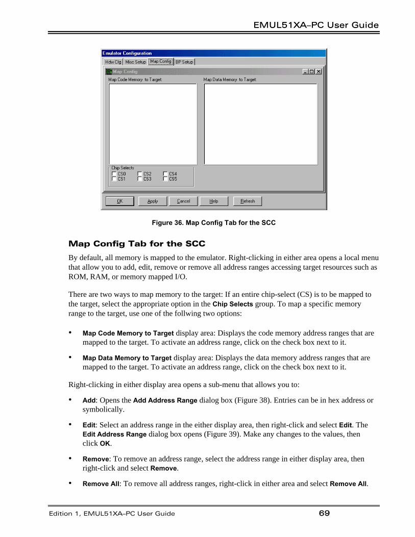
EMUL51XA–PC User GuideEMUL51XA–PC User Guide
Edition 1, EMUL51XA–PC User Guide 6969
Figure 36. Map Config Tab for the SCC
Map Config Tab for the SCC
By default, all memory is mapped to the emulator. Right-clicking in either area opens a local menuthat allow you to add, edit, remove or remove all address ranges accessing target resources such asROM, RAM, or memory mapped I/O.
There are two ways to map memory to the target: If an entire chip-select (CS) is to be mapped tothe target, select the appropriate option in the Chip Selects group. To map a specific memoryrange to the target, use one of the follwing two options:
• Map Code Memory to Target display area: Displays the code memory address ranges that aremapped to the target. To activate an address range, click on the check box next to it.
• Map Data Memory to Target display area: Displays the data memory address ranges that aremapped to the target. To activate an address range, click on the check box next to it.
Right-clicking in either display area opens a sub-menu that allows you to:
• Add: Opens the Add Address Range dialog box (Figure 38). Entries can be in hex address orsymbolically.
• Edit: Select an address range in the either display area, then right-click and select Edit. TheEdit Address Range dialog box opens (Figure 39). Make any changes to the values, thenclick OK.
• Remove: To remove an address range, select the address range in either display area, thenright-click and select Remove.
• Remove All: To remove all address ranges, right-click in either area and select Remove All.

Chapter 4. Installing and Configuring the Seehau SoftwareChapter 4. Installing and Configuring the Seehau Software
7070 EMUL51XA–PC User Guide
Figure 37. BP Setup Tab
BP Setup Tab
The BP Setup tab (Figure 37) configures hardware breakpoint ranges.
• Hardware Breakpoints display area: Displays the address ranges that are enabled for hardwarebreakpoints.
• Add: Opens the Add Address Range dialog box (Figure 38). Entries can be done with hexaddress or symbolically.
• Edit: Select an address range in the Hardware Breakpoints display area, then click Edit. TheEdit Address Range dialog box opens (Figure 39). Make any changes to the values, then clickOK.
• Remove: To remove an address range, select the address range in the Hardware Breakpointsdisplay area, then click Remove.
Add Address Range Dialog Box
• Start address: Enter the starting address of the range.
• End address: Enter the ending address of the range
• OK: Saves the settings and closes the dialog box.
• Cancel: Exits the dialog box without saving the settings.
• Help: Displays the Seehau Help file.

EMUL51XA–PC User GuideEMUL51XA–PC User Guide
Edition 1, EMUL51XA–PC User Guide 7171
Edit Address Range Dialog Box
• Start address: Enter the starting address of the range. (If you have highlighted a range in theHardware Breakpoints display area, this range shows in the Start address and End addressfields.)
• End address: Enter the ending address of the range
• OK: Saves the settings and closes the dialog box.
• Cancel: Exits the dialog box without saving the settings.
• Help: Displays the Seehau Help file.
Figure 38. Add Address Range Dialog Box
Figure 39. Edit Address Range Dialog Box

Chapter 4. Installing and Configuring the Seehau SoftwareChapter 4. Installing and Configuring the Seehau Software
7272 EMUL51XA–PC User Guide

EMUL51XA–PC User GuideEMUL51XA–PC User Guide
Edition 1, EMUL51XA–PC User Guide 7373
Introduction to Tracing
Overview
Trace is a comprehensive tool used to analyze the microprocessor environment. While using trace,you can passively analyze user code in real time as the code continues to execute. Without trace,however, the emulator only provides a snapshot of the processor environment.
The trace feature provides the same basic capabilities as a logic analyzer. Each trace frame istimestamped and records the following fields: address and data values, cycle type, and up to 18external inputs. Based on various combinations of these fields, you can set up trigger and/or filterconditions to control the trace recording.
By default, the trace automatically starts recording when you begin user code execution. Whenyou stop code execution, the trace history is displayed automatically.
Trace allows you to perform many tasks, including:
• Detecting an error condition
• Analyzing a history of the sequence of events leading to an error
• Characterizing code behavior using Code Coverage.
• Sampling time measurements
• Analyzing peripheral I/O
The Seehau software provides a symbolic interface for both the trace setup and display.
A trace history is a time ordered recording of bus cycles (with some other helpful information).Events that do not affect the CPU external bus, such as testing a CPU internal register, are not re-corded. Events that do affect the bus will only be recorded if Trace Setup is instructed to recordthose types of events. All tracing emulators record bus events and not actual instruction execution,so they all must have some way to deal with the effects of the instruction pipeline. The Nohautrace board includes pipeline decoding and marks opcode fetches that are not executed. Therefore,the display software can show the trace records as though the pipeline did not exist. Optionally, itcan also display the uncorrected bus cycles just as they were recorded.
Normal Mode
Tracing starts automatically every time emulation starts. Single stepping turns on the trace re-cording during that step. The trace buffer continues to collect records until recording is stopped.Tracing is stopped in one of the following ways:
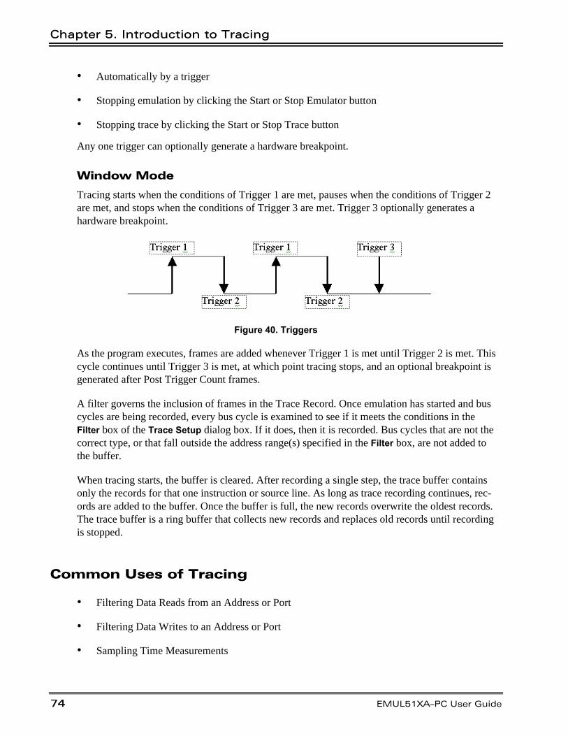
Chapter 5. Introduction to TracingChapter 5. Introduction to Tracing
7474 EMUL51XA–PC User Guide
• Automatically by a trigger
• Stopping emulation by clicking the Start or Stop Emulator button
• Stopping trace by clicking the Start or Stop Trace button
Any one trigger can optionally generate a hardware breakpoint.
Window Mode
Tracing starts when the conditions of Trigger 1 are met, pauses when the conditions of Trigger 2are met, and stops when the conditions of Trigger 3 are met. Trigger 3 optionally generates ahardware breakpoint.
Figure 40. Triggers
As the program executes, frames are added whenever Trigger 1 is met until Trigger 2 is met. Thiscycle continues until Trigger 3 is met, at which point tracing stops, and an optional breakpoint isgenerated after Post Trigger Count frames.
A filter governs the inclusion of frames in the Trace Record. Once emulation has started and buscycles are being recorded, every bus cycle is examined to see if it meets the conditions in theFilter box of the Trace Setup dialog box. If it does, then it is recorded. Bus cycles that are not thecorrect type, or that fall outside the address range(s) specified in the Filter box, are not added tothe buffer.
When tracing starts, the buffer is cleared. After recording a single step, the trace buffer containsonly the records for that one instruction or source line. As long as trace recording continues, rec-ords are added to the buffer. Once the buffer is full, the new records overwrite the oldest records.The trace buffer is a ring buffer that collects new records and replaces old records until recordingis stopped.
Common Uses of Tracing
• Filtering Data Reads from an Address or Port
• Filtering Data Writes to an Address or Port
• Sampling Time Measurements

EMUL51XA–PC User GuideEMUL51XA–PC User Guide
Edition 1, EMUL51XA–PC User Guide 7575
Basic Features of Tracing
• Trigger: An event that stops trace buffer recording.
• Delay: The number of trace frames collected after a trigger event occurs.
• Filter: A set of conditions that determine which frames are allowed into the trace buffer.
• Timestamp: A feature that displays the number of machine cycles that have elapsed since thebeginning of program execution.

Chapter 5. Introduction to TracingChapter 5. Introduction to Tracing
7676 EMUL51XA–PC User Guide

EMUL51XA–PC User GuideEMUL51XA–PC User Guide
Edition 1, EMUL51XA–PC User Guide 7777
Configuring the Trace Board
Trace Window
The contents of the trace buffer are displayed in the Trace window (Figure 41). To open a Tracewindow, use the TR button on the toolbar, or, from the New menu, select Trace.
The Trace menu controls most of the Trace window features. (See the “Trace Menu” section.)
• Frame Number is on the far left of the window. Frame 0 always represents the trigger frame.If there is no trigger, frame 0 is the last frame in the buffer.
• Address displays the address of the bus cycle in hexadecimal notation.
• Timestamp displays the number of machine cycles that have elapsed since the beginning ofprogram execution. Relative timestamp can also be set up. This will display the number ofmachine cycles that have elapsed since the last instruction.
• Data displays bytes of data from the displayed bus cycle.
• Status shows the cycle type: First byte of Fetch, Write, Read, or other frames (shown with adash).
• Instr. shows the instruction disassembly.
• Symbol shows any symbolic label that refers to a specific address.
Figure 41. Trace Window

Chapter 6. Configuring the Trace BoardChapter 6. Configuring the Trace Board
7878 EMUL51XA–PC User Guide
Figure 42. Trace Menu
Trace MenuTo access the Trace menu, right-click in the Trace window or select the Trace menu whichappears in the main menu bar only when the Trace window is active (Figure 42).
• Go to Frame number: Brings up a dialog box where you can enter a specific frame number fordisplay.
• Find Trigger Point: Displays the trigger point (frame zero).
• Zero Time at Cursor: Changes the timestamp at the selected frame to zero and makes all othertimestamps relative to the selected frame.
• Synchronize Source Window: Automatically aligns the display of code in the Source windowas you scroll through the Assembly code in the trace buffer. You must use the up/down arrowkeys in conjunction with this feature.
• Display mode: Brings up a sub-menu that allows you to select which code to display:
– Trace Only: Displays Assembly code only in the trace buffer.
– Mixed (Trace and Source): Displays both C and Assembly code in the trace buffer.
– Source Only: Displays C source code only in the trace buffer.

EMUL51XA–PC User GuideEMUL51XA–PC User Guide
Edition 1, EMUL51XA–PC User Guide 7979
• Find: Brings up the Find Address dialog box where you can search the trace buffer for anaddress or a range of addresses and a cycle type.
– Address to find: Enter a start address to search for. Enter an end address to search for arange.
– Search from: Enter a frame number to begin your search or select Entire to search theentire trace buffer.
– Cycle type: Select one cycle type from the following choices:# Opcode# Read Data# Write Data# Read OR Write Data# All
• Find Next: Click to find the next frame match.
• Find Previous: Click to find the previous frame match.
• Show Source Line: Displays the associated source code for the current frame. The frameaddress must match a source line address.
• File
– Save to File: Opens the Save Trace to File dialog box where you can save the contents ofthe trace buffer as text to a file (Figure 43).
– Print: Opens a dialog box for printing any portion of the trace buffer in any display mode.Only the fields displayed in the Trace window are printed.
Figure 43. Save Trace to File Dialog Box

Chapter 6. Configuring the Trace BoardChapter 6. Configuring the Trace Board
8080 EMUL51XA–PC User Guide
Note
The following menu items can be toggled individually or can be configured all at
once. Click All Options to bring up the Display Options dialog box.
• Show TimeStamp: Displays the timestamp which represents the number of machine cyclesthat have elapsed since the beginning of program execution.
• Relative TimeStamp: Displays the timestamp as the number of machine cycles elapsed sincethe execution of the previous instruction.
• Convert Cycles to Time: Converts the timestamp from machine cycles to actual time based onthe microprocessor clock (uP clock).
• Show Misc.: This option displays 24 bits (shown as a hex byte and a hex word) for each rec-ord. The far left byte displays the eight external input bits from the DB15 connector.
• Show Internal Bus: This option displays the code that executes in internal code RAM underseparate columns.
• Show External Bus: This option displays external code and Read/Write bus cycles underseparate columns.
• Show Pod Pins 7..0: Displays the recorded status of external logic signals connected to thetrace array on the pod.
• Show Data: Displays the data field.
• Show Status: Displays bus cycle type (Fetch, Write, or Read).
• Show Symbol: Displays symbolic labels associated with the address field.
• Compressed: Displays assembly code only.
• All Options: Opens the Display Options dialog box where you can select or clear trace optionsin a single update.
• Trace Config: Opens the Trace Configuration window. Refer to the following “TraceConfiguration Window” section.
• Settings: Bring up a sub-menu that allows you to set the color, font, status bar and columnsize for the Trace window.
• Caption: Allows you to change the Trace window caption in the title bar.

EMUL51XA–PC User GuideEMUL51XA–PC User Guide
Edition 1, EMUL51XA–PC User Guide 8181
Figure 44. Trace Configuration Window Displaying the Trace Setup Tab
Trace Configuration Window
To open the Trace Configuration window, select Trace Config from the Trace menu, or selectConfig from the main menu, then Trace (Figure 44). This window has five tabs:
• Trace Setup
• Trigger1
• Trigger 2
• Trigger 3
• Filter
Buttons Common to All Tabs
OK—Saves the settings for this tab and closes the Trace Configuration window.
Apply—Saves the settings for this tab.
Cancel—Exits without saving the settings for the tab.
Help—Opens the Seehau Help file.
Refresh—Allows you to retrieve and view the current trace and emulator hardware configurationsettings.

Chapter 6. Configuring the Trace BoardChapter 6. Configuring the Trace Board
8282 EMUL51XA–PC User Guide
Trace Setup Tab
• Trace Type: Displays the trace type that you selected during the initial configuration.To change this, run Seehau Config. From the Start menu, select Programs. Then selectSeehauXA and click Config from the sub menu. The Emulator Configuration window opensdisplaying the Connect tab.
• I/O Address: Displays the address of the trace board you selected during the initial configura-tion. To change this, run Seehau Config. From the Start menu, select Programs. Then selectSeehauXA and click Config from the sub menu. The Emulator Configuration window opensdisplaying the Connect tab.
• Trace Memory Size: Displays the trace memory size.
• Break Emulation?
– Yes, on Trigger: This option provides hardware breakpoint capability. In the NormalFilter mode, the first trigger meeting the conditions causes the breakpoint. In the WindowFilter mode, Trigger 3 meeting the conditions causes the breakpoint.
– Yes, on Trace Stop: This is a rarely used option that allows stopping both emulation andtrace by clicking Start or Stop Trace (clicking Start or Stop Emulation does the samething).
• Recording Per Clock: (Rev. D trace only) By default, the trace is recorded per frame (per buscycle). When Recording Per Clock is selected, the trace is recorded for each processor clockcycle.
• ReadCycle Include MOVC: By default, the read cycle includes just the data read cycle. Whenthis option is selected, the code read cycle (the MOVC instruction ) is counted as the readcycle.
• Active Triggers
– Triggers 1, 2 and 3: This option is a quick way to enable or disable software and hardwaretriggers and the filter. Software Trigger 2 can only be used if Trigger 1 is used, andTrigger 3 can only be used if Trigger 2 is used.
– Filter: This option filters your trace captures, and selects the type of information in anaddress range, and the type of data that is recorded in the trace memory.
– External Trig: An external event that stops trace buffer recording (allows a signal on theexternal trigger to generate a trigger).
• Last Trigger Repeat Count: You can specify a trigger to occur when a condition is met for thenth time.
• Internal Bus: The address of the data bus inside of the MCU.
• Post Trigger Count: Specifies the number of frames to be recorded after the trigger hasoccurred.

EMUL51XA–PC User GuideEMUL51XA–PC User Guide
Edition 1, EMUL51XA–PC User Guide 8383
• External Bus: The address of the data bus outside of the MCU.
• Target Vcc
– 3.3 Volt: Low voltage option for some pods.
– 5.0 Volt: Voltage requirement for some pods.
• Filter Mode
– Normal: Trigger 1, Trigger 2, and Trigger 3 form a sequence of conditions to stop tracerecording.
– Window: Trigger 1 starts trace recording, Trigger 2 pauses trace recording, Trigger 3stops trace recording.
• Trigger Mode
– Opcode: You have the option to select the type of cycle the trigger will trigger ON, whenyou enter a trigger.
– Data: You have the option to select the type of cycle the trigger will trigger ON, when youenter a trigger.
• Trigger Memory Mapping: For the 256K trace board, there is only 256K of trigger memory inthe trace board. The 256K trigger memory can be relocated to any 256K block location in therange from 000000H to 3FFFFFH. For the 1-MB trace board, there is only 1 MB of triggermemory in the trace board. The 1-MB trigger memory can be relocated to any 1-MB blocklocation in the range from 000000H to FFFFFFH.
Figure 45. Trigger 1 Tab

Chapter 6. Configuring the Trace BoardChapter 6. Configuring the Trace Board
8484 EMUL51XA–PC User Guide
Trigger 1, 2 and 3 Tabs
Clicking any of the Trigger tabs displays a screen that lets you configure the trigger (Figure 45).Each configuration screen is divided into two areas:
• Address Cycle Type
• Data Trigger Type
In the Address Cycle Type and Data Trigger Type text boxes, you can enter numerous conditions,which are logically ORd. These two windows are then logically ANDd together to satisfy the trig-ger specification for the particular Trigger tab. You can also leave either the Address Cycle Typeor the Data Trigger Type blank.
• Enable Trigger: Selecting this option enables the trace to be controlled by a trigger. The trig-ger will cause the trace to start recording and continue until the post trigger count has reachedzero. At that time, trace recording stops, and you can view the results in the Trace window.
• Data Mask: Selects the comparison mask for the data value. Set the bits that you want toqualify with a number 1 and those bits that you don't care about can be set as 0.
• Address Mask: The mask is used as an alternate method to create address ranges. The addressmask value is logically ANDd with the address value. A zero in the result corresponds to aDon’t Care in the address value.
• Clr Trigger1: Clears all the settings for the currently selected trigger.
Filter Tab
The Filter tab displays options that lets you configure the filter (Figure 46). This tab is divided intotwo areas:
• Address Cycle Type
• Data Trigger Type
In the Address Cycle Type and Data Trigger Type text boxes, you can enter numerous conditions,which are logically ORd. These two windows are then logically ANDd together to satisfy the trig-ger specification for the Filter tab. You can also leave either the Address Cycle Type or the DataTrigger Type blank.
• Enable Filter: Selecting this option activates the filter. Clearing this option disables the filterfrom collecting data. However, the filter information will be saved.
• Extended Recording: Selecting this option enables the trace memory to continue recordingfor a specified number of cycles after the trigger has happened. This captures some cycles af-ter the trigger event has occurred.

EMUL51XA–PC User GuideEMUL51XA–PC User Guide
Edition 1, EMUL51XA–PC User Guide 8585
Figure 46. Filter Tab
• Data Mask: Selects the comparison mask for the data value. Set the bits that you want toqualify with a number 1 and those bits that you don't care about can be set as 0.
• Address Mask: The mask is used as an alternate method to create address ranges. The addressmask value is logically ANDd with the address value. A zero in the result corresponds to aDon’t Care in the address value.
• Clr Filter: Clears all the settings in the filter selection of the Trace Setup tab.
Trigger Qualifier Dialog Box
Right-clicking in the Address Cycle Type area in any Trigger or in the Event tabs opens a sub-menu where you can select to add, remove or edit trigger options and address ranges. ClickingRemove deletes the highlighted range. Clicking Add or Edit opens the Trigger Qualifier dialog box(Figure 47).
• Include All: Triggers on Opcode Fetch or Data R/W.
• Opcode Fetch: Triggers when an opcode is fetched.
• Data R/W: Triggers on any Data R/W.
• Exclude All: This line is inactive.
• Address Range
– Start: Specifies the beginning of the trigger address range
– End: Specifies the end of the trigger address range (inclusive).

Chapter 6. Configuring the Trace BoardChapter 6. Configuring the Trace Board
8686 EMUL51XA–PC User Guide
Figure 47. Trigger Qualifier Dialog Box
Data Qualifier Dialog Box
Right-clicking in the Data Trigger Type area in any Trigger or in the Event tabs opens a sub-menuwhere you can select to add, remove or edit trigger options and data ranges. Clicking Remove de-letes the highlighted range. Clicking Add or Edit opens the Data Qualifier dialog box (Figure 48).
• Trigger Mode
– Range: Triggers on a range of data (numerical progression).
– Pattern: Triggers on a data pattern (1’s and 0’s).
• Data Range
– Start: Specifies the beginning of the trigger data range
– End: Specifies the end of the trigger data range (inclusive).
Figure 48. Data Qualifier Dialog Box

EMUL51XA–PC User GuideEMUL51XA–PC User Guide
Edition 1, EMUL51XA–PC User Guide 8787
Pod Adapters
Overview
Pod adapters can be the weakest link in a project where emulators are used. They can be a constantsource of problems, or they can be virtually problem free. It is up to you to make the decision onhow to adapt the emulator to your target. This chapter discusses the following methods:
• Direct pin-to-socket
• Solder-down
Direct Pin-to-Socket Connection
If you design your target with corresponding pin sockets, you will have an inexpensive, reliableconnection to the emulator.
Solder-Down Adapter
The next best choice is a solder-down adapter. To use this option, you must remove the targetprocessor. A professional should do soldering in the base. Nohau recommends two companies thatprovide this service if you do not have this in-house capability:
• Business Electronics Soldering Technologies, Inc. (BEST, Inc.) (847) 797-9250
• Emulation Technology, (800) 232-7837
Once the base is correctly in place, carefully align the attaching boards to hook up to the emulator.These adapters are fairly expensive, but if done correctly provide a solid connection that shouldnot give you any problems.
C3, G3 and G49 Pod Adapters
This section describes the pod-to-target adapters for the Philips XA–C3, G3 and G49 microcon-troller family See Hlp_JumpersXA in Seehau Help for a list of the pods covered by this chapter.
The best way to design your target system for emulatability is with a pin-to-socket connection.Figure 49 shows the outline of the connectors coming off the underside of the pod. Connectorsare referred to collectively as J4, consist of 44 headers, that connect to pins on the chip.

Chapter 7. Pod AdaptersChapter 7. Pod Adapters
8888 EMUL51XA–PC User Guide
6.35 in.
4.
1
in
.
Adapter
Orientation(insert on bottom)
Pin 1
1 in.
2.5 cm.
1 in.
2.5 cm.
The 44-pin PGA connector
is used with a 44-pin PGA
to 44-pin PLCC adapter,
requiring one inch of
space above the target.
TOP VIEW
JP1
JP2
JP24
JP25
JP11
JP12
JP23
JP18
JP28
JP15
JP
3J
P4
JP
5J
P6
JP
7J
P8
JP
9J
P1
0
JP26
JP22
JP19
JP20
JP27
JP21
JP16JP13
J2J1
JP14
Figure 49. Pin-to-Socket Connections for the XA–C3 Adapter
Solder-Down Adapters
Following is a list of the solder-down adapters available for the EMUL51XA–C3, G3,and G49:
• EDI / 44PG/PL-L—Adapter to plug 44-pin pod into 44-pin PLCC socket.
• EDI / 44PG/LC-SD—Adapter assembly, 44-pin PGA socket to 44-pin PLCC, to solder touser target board. Includes one top and one EDI/44LC-SD base.
• EDI / 44LC-SD—Additional base only. 44-pin PLCC solder-down base for theEDI/44PG/LC-SD.
• EDI / 44PG/QFS31-SD—Adapter assembly, 44-pin PGA socket to 44-pin LQFP, to solder touser target board. Includes one top and one EDI/44QFS31-SD base.
• EDI / 44QFS31-SD—Additional base only. 44-pin LQFP solder-down base for theEDI/44PG/QFS31-SD.
• MCK 44-PGA/PLCC—McKenzie adapter for a 44-pin PGA socket to a 44-pin PLCC plug.

EMUL51XA–PC User GuideEMUL51XA–PC User Guide
Edition 1, EMUL51XA–PC User Guide 8989
Figure 50. Typical Solder-Down Adapter for C3, G3 and G49
0.70 in.
2.35 in.
6.35 in.
2.
92
5
in
.
1.
12
5
in
.
4.
1
in
.
Front
Pin 1
Adapter Orientation(insert on bottom)
1.75 in.
1.745 in.
72-Pin Connector
Location ofthe 72-PinConnector
Figure 51. Target Interface for the S3

Chapter 7. Pod AdaptersChapter 7. Pod Adapters
9090 EMUL51XA–PC User Guide
S3 Pod Adapters
This section describes the pod-to-target adapters for the Philips XA–S3 microcontroller family.See Hlp_JumpersXA in Seehau Help for a list of the pods covered by this chapter.
Figure 51 shows the top view of the adapter looking through the pod board (top of board with theDB-25 connector on the left). The pin numbers are suitable for the 68-pin PLCC version of theXA–S3. The ES/110-7393-80 adapter for the 80-pin LP–PQFP socket translates this pinout to oneappropriate for the QFP package.
Direct Pin-to-Socket Connections
The best way to design your target system for emulatability is with a pin-to-socket connection.Figure 52 shows the outline of the connectors coming off the underside of the XA/S3/IE pod.Connectors are referred to collectively as J4, consist of four sets of 9x2 industry-standard (72 pins)that connect to pins on the chip.
The choice of adapters is influenced by the number of pins of the target chip. The number of pinson the bottom of the pod stays as 72 pins, since the same pod is used for all members of the XA–S3 family. However, the package and the number of pins on the chip change, determining theshape and size of the base. The following shows the package and number of pins for processors inthe XA–S3 family:
Chip Package Number of Pins
XA-S3 PLCC 68
XA-S3 LP-PQFP 80
Figure 52. Typical Solder-Down Adapter for S3

EMUL51XA–PC User GuideEMUL51XA–PC User Guide
Edition 1, EMUL51XA–PC User Guide 9191
Following is a list of the solder-down adapters available for the EMUL51XA–S3:
• ES/110-2711-00—Adapter for a 44-pin PLCC socket that is used for emulation of theXA-G3 with the XA-S3.
• ET/AP4-68-SUB1—Adapter for a 68-pin PLCC socket.
• MCK/ADP-68PGA/PLCC—McKenzie adapter for a 68-pin PGA socket to a 68-pinPLCC plug.
• ES/000-4532—Additional base only. 80-pin LQFP solder-down base for theEDI/110-7393-80.
SCC / H3 / H4 Pod Adapters
This section describes the pod-to-target adapters for the Philips XA–SCC/H3/H4 microcontrollerfamily. See Hlp_JumpersXA in Seehau Help for a list of the pods covered by this chapter.
Figure 53 shows the top view of the adapter looking through the pod board (top of board with theDB-25 connector on the left). The ET/EPP100QF49W adapter for the 100-pin LQFP socket trans-lates this pinout to one appropriate for the QFP package.
Figure 53. Target Interface for the SCC/H3/H4

Chapter 7. Pod AdaptersChapter 7. Pod Adapters
9292 EMUL51XA–PC User Guide
Solder-Down Adapters
Following is a list of the solder-down adapters available for the EMUL51XA–SCC/H3/H4:
• ET/EPP100QF49W—Adapter for a 100-pin LQFP. Includes one top and oneET/EPP100F49SM base.
• ET/EPP100QF49SM—Additional base only. 100-pin LQFP solder-down base for theET/EPP100QF49W.
0.735 in.
18.63 mm.
Adapter Disconnected
0.335 in.
8.52 mm.
0.815 in.
20.71 mm.
Adapter Connected
0.335 in.
8.52 mm.
Figure 54. Typical Solder-Down Adapter for SCC/H3/H4

EMUL51XA–PC User GuideEMUL51XA–PC User Guide
Edition 1, EMUL51XA–PC User Guide 9393
Troubleshooting
Overview
Features of the EMUL51XA–PC that make your troubleshooting easier include on-screen errormessages and the emulator Status window, (which consists of one or more words inside bracketsin the upper right corner of the screen).
The error messages time out during byte transmission or time out during byte reception or hard-ware not responding indicate that communication between the emulator and the PC is notworking.
The troubleshooting steps in this chapter are organized into groups according to whether or not theemulator had been working before the trouble symptoms appeared:
Not Working In Stand-Alone Mode—Emulator is being installed in computer for the first timeor it will not start up or run when the pod is not connected to a target.
Not Working With New Target System—Emulator has been running in stand-alone mode previ-ously, but will not start in the target system.
No Longer Working in Target System—Emulator has been running while plugged into thetarget system, but is no longer working.
Note
Nohau is continuously updating, enhancing, and fixing the Seehau software
interface. These latest versions are available on the Nohau website. If you are
having any problems, verify that the software version you are using is the latest.
If not, visit www.nohau.com and download the latest Seehau software version.
Not Working in Stand-Alone Mode
When a system is first received or picked up after sitting on the shelf for a long period of time, it isrecommended that you start the emulator system in the stand-alone mode first, before plugging itinto a target. Stand-alone mode is when the pod is plugged into the communications interface (forexample, an EPC cable) but not plugged into the target.

Chapter 8. TroubleshootingChapter 8. Troubleshooting
9494 EMUL51XA–PC User Guide
If the emulator attempts to start up in stand-alone mode but fails, a configuration window isopened and then an error message opens on top of that window. Typically, this is a general errorstating that the software can not communicate with the pod. To investigate this problem, do thefollowing:
1. Reference the manual or the online Help and set the pod jumpers back to the default or factorysettings.
2. Confirm that the cable between the pod and the PC is properly connected. This will be differ-ent depending on the communications interface purchased.
3. In the software configuration screen, verify that the correct communications interface is se-lected. If this is an EPC connection and you are using LPT1, verify that the PC uses address378H for LPT1.
4. In the software configuration screen, verify that the correct pod type is selected. The 25-pinconnector on the pod has a white sticker that has the pod type that should be selected. There isalso the selection for Internal or External. This setting must match the Ext. Mode jumper set-ting on the pod.
5. Verify that the controller chip is getting power and clock. This should be measured at the con-troller chip itself.
6. If the system still will not start up, and there is a trace board attached to the pod, remove thetrace board. Remember to go through the configuration again and select No Trace.
7. Contact Nohau Technical Support.
Not Working With New Target System
If the emulator has been running in stand-alone mode, but will not work in a new target system,perform the following steps:.
Software Will Not Start Up (Fatal Error)
1. Verify that power is present on the target system (even if you have internal power selected).
2. Verify that the controller is still getting a clock. If the crystal jumpers have been moved to theTARGET position, try moving them back to the POD position even though the pod is pluggedinto the target. If this works, check the adapter an open or short.
3. Check address bus, data bus and control bus signals for shorts to VCC or GND, and for incor-rect connections to anything else on the target system. This could indicate an issue with thetarget or the adapter.
4. Check adapter for opens or shorts.

EMUL51XA–PC User GuideEMUL51XA–PC User Guide
Edition 1, EMUL51XA–PC User Guide 9595
5. The emulator will not work properly if the reset line is being pulled low from the target systemor you have a watchdog timer (or similar circuitry) on the target. When the emulator is inmonitor mode (not running customers code), we are not servicing the watchdog timer on thetarget and it will reset the controller and cause the emulator to crash. Either disconnect thewatchdog timer, or remove the Reset jumper on the pod. This will disconnect the reset line onthe target from the reset pin on the processor.
6. Nohau sells a tool called an isolator ISO-160 which helps to determine which line is causingthe problems when plugged into a target. This is an additional adapter that has dip switches foreach line. Simply connect this between the pod and the adapter with all the switches open.This should be the same as in stand-alone mode and come up fine. Then slowly introduce linesuntil the line that is causing the problem is determined.
7. Contact Nohau Technical Support.
Software Starts Up, But Code Will Not Execute Properly
1. Verify that the stack is set up properly and located in valid memory space.
2. Verify that any memory mapped I/O devices are mapped to the target, otherwise the pod willjust write to the emulator’s memory and not to the target’s memory or devices. This can be setfrom the Config menu, selecting Emulator, and then selecting the Memory Map tab. By open-ing an XDATA window, you can also manually write to a memory mapped device on the tar-get at a specific address to verify the signals and data are actually going to the target.
3. Single-step through the code at either the assembly or source level to determine exactly whatis not working and where the failure occurs. Once this has been determined, if it is not clear,contact Nohau Technical Support.
No Longer Working in Target System
If the emulator has been working in the target system, but is no longer working, Go back to thestand-alone mode with all default settings. If this fails, see the previous section “Not Working inStand-Alone Mode.” If this passes, connect back to target with pod power and pod crystal. If itpasses, check the adapter for loose, short, or open connection. If it still fails, move the pod crystalback to target and see the previous section “Software Will Not Start Up (Fatal Error).”

Chapter 8. TroubleshootingChapter 8. Troubleshooting
9696 EMUL51XA–PC User Guide

EMUL51XA–PC User GuideEMUL51XA–PC User Guide
Edition 1, EMUL51XA–PC User Guide 9797
Index1
12- and 16-bit headers
POD-51XA-S3 · 43
POD-51XA-G3/G49/C3 · 31
1st BKPT Mem Rel · 60, 65
1st BKPT Mem Rel – 4th BKPT Mem Rel · 61, 65
1st Code/Data Rel – 4th Code/Data Rel · 61, 65
2
2000 PRO Device Manager Window (screen shot) · 19
25-pin D connector · 6
2nd BKPT Mem Rel · 60, 65
3
3.3 Volt (Trace Setup tab) · 83
5
5.0 Volt (Trace Setup tab) · 83
5V and 3V header
POD-51XA-G3/G49/C3 · 29
POD-51XA-S3 · 41
POD-51XA-SCC · 50
9
90-day warranty · v
adapter · v
cable · v
externder · v
A
A12 – A19 headers · 32
A12 – A23 headers for the S3 · 44
Active Triggers (Trace Setup tab) · 82
Adapter Dimensions for the POD–51XA–G3 / G49 / C3(diagram) · 26
Adapter Dimensions for the POD–51XA–S3 (diagram) · 38
Adapter Dimensions for the POD–51XA–SCC (diagram) · 49
Add Address Range Dialog Box · 70
Add Address Range Dialog Box (screen shot) · 71
Address · 77
Address Cycle Type (Filter tab) · 84
Address Cycle Type (Trigger 1, 2 and 3 tabs) · 84
Address Mask (Filter tab) · 85
Address Mask (Trigger 1, 2 and 3 tabs) · 84
Address Range (Trigger Qualifier dialog box) · 85
Address to find (Trace menu) · 79
administrative privileges
EPC
Windows 2000 · 16–15
Windows NT · 15–14
LC-ISA plug-in board
Windows 2000 · 11–10
Windows NT · 8–7
USB with Windows 2000 · 16–15
All Options (Trace menu) · 80
alternate address · 8, 10, 13
Alternate Address Settings for the Emulator Header J1(diagram) · 6
Application Notes for the SCC
bank swapping · 52
Loading files larger than 256K · 52
TXsignal on UART1 and UART2 · 54
UART/DMA bondout bug · 53
B
Basic Hardware · 1
Bondout Microcontroller · 23, 24, 36, 48
BP Setup · 62
BP Setup Tab
adding an address range · 70
editing an address range · 70
hardware breakpoint · 70
removing an address range · 70
BP Setup Tab (screen shot) · 70
Break Emulation (Trace Setup tab) · 82
Bus Width · 60, 61, 65, 66
Business Electronics Soldering Technologies, Inc. · 87
C
C3, G3 and G49 pod adapters · 87
available adapters · 88
connections (diagram) · 88

IndexIndex
9898 EMUL51XA–PC User Guide
target interface (diagram) · 89
typical adapter (diagram) · 89
Caption (Trace menu) · 80
Chip Selects · 69
Clock (MHz) · 60, 61, 65, 66
Clock headers
POD-51XA-G3/G49/C3 · 27
POD-51XA-S3 · 39
POD-51XA-SCC · 49
Clr Filter (Filter tab) · 85
Clr Trigger1 (Trigger 1, 2 and 3 tabs) · 84
Code header
POD-51XA-S3 · 43
POD-G3/G49/C3 · 31
Code Mem Relocate · 59, 64
Code Will Not Execute Properly, troubleshooting · 95
Communications Interface · 57
Communications Interfaces
Emulator Parallel Cable (EPC) · 3
High-Speed Parallel Box (HSP) · 3
Industry Standard Architecture (ISA) · 3
Low-Cost Industry Standard Architecture (LC-ISA) · 4
Universal Serial Bus (USB) · 4
Compressed (Trace menu) · 80
Computer Management Window With the Drivers FolderSelected (screen shot) · 14
Computer Management Window With the I/O Folder Selected(screen shot) · 13
configuring
communications interface · 3
emulator options · 57
Seehau · 18–17
trace board · 77
Configuring the Emulator Options
Connect Tab · 57
Hdw Cfg Tab · 58
Hdw Cfg Tab for the SCC · 61
Configuring the Emulator Options From Within Seehau
adding address ranges · 70
configuring hardware breakpoint ranges · 70
editing address ranges · 71–70
mapping address ranges · 67
mapping address ranges for the SCC · 69
selecting reset options · 67
setting up emulator hardware options · 63
setting up emulator hardware options for the SCC · 65–64
Connect tab · 20, 24, 36, 48, 57, 63, 65, 82
Connect Tab · 57
communications interface · 57
emulator board address · 57
select processor · 57
trace type · 57
Connect Tab Displaying USB Selected (screen shot) · 21
Convert Cycles to Time (Trace menu) · 80
create file failed error · 9, 14, 15, 17
CS4 (P3.0) · 62, 66
CS5 (P3.1) · 62, 66
cycle type · 77
Cycle type (Trace menu) · 79
D
Data · 77
Data (Trace Setup tab) · 83
Data / Address Bus Configurations
G3, G49 and C3 pods · 33
S3 pod · 45
Data Mask (Filter tab) · 85
Data Mask (Trigger 1, 2 and 3 tabs) · 84
Data Mem Relocate · 59, 64
Data Qualifier dialog box
Data Range · 86
Trigger Mode · 86
Data Qualifier Dialog Box (screen shot) · 86
Data R/W (Trigger Qualifier dialog box) · 85
Data Range (Data Qualifier dialog box) · 86
Data Trigger Type (Filter tab) · 84
Data Trigger Type (Trigger 1, 2 and 3 tabs) · 84
debugger application · v
default address range for the LC–ISA card · 8, 10, 12
Default Position for Header JP1 (diagram) · 7
Default Settings for the Emulator Header J1 (diagram) · 6
Delay · 75
Device Manager tab · 10, 19
dialog boxes
Add Address Range · 70
Data Qualifier · 86
Display Options · 80–79
Edit Address Range · 71–70
Find Address · 79–78
Local Group Properties · 8
Save Trace to File · 79–78
Setup Complete · 56–55
Trigger Qualifier · 85
User Manager · 8
Dimensions

EMUL51XA–PC User GuideEMUL51XA–PC User Guide
Edition 1, EMUL51XA–PC User Guide 9999
POD-51XA-G3/G49/C3 · 26
POD-51XA-S3 · 38
POD-51XA-SCC · 49
Direct Pin-to-Socket Connection · 87
Display mode (Trace menu) · 78
Downloading product documentation · vii
DRAM (CS1) · 62, 66
E
EDI / 44LC-SD · 88
EDI / 44PG/LC-SD · 88
EDI / 44PG/PL-L · 88
EDI / 44PG/QFS31-SD · 88
EDI / 44QFS31-SD · 88
Edit Address Range Dialog Box · 71
Edit Address Range Dialog Box (screen shot) · 71
Emulation Memory
POD-51XA-G3/G49/C3 · 26
POD-51XA-S3 · 38
POD-51XA-SCC · 51
Emulation Memory Config · 58, 63
Emulation Technology · 87
Emulator Board Address · 57
emulator board, warranty · v
emulator cable, warranty · v
Emulator Configuration Window Displaying the Connect Tab(screen shot) · 57
Emulator Configuration Window Displaying the Hdw CfgTab (screen shot) · 58
Emulator Configuration Window Displaying the Hdw CfgTab for the SCC (screen shot) · 61
Emulator Parallel Cable (EPC) · 3
Emulator Parallel Cable (photo) · 4
EMUL—PC/USB Connections (photo) · 19
Enable Filter (Filter tab) · 84
Enable Trigger (Trigger 1, 2 and 3 tabs) · 84
Enlargement of POD–51XA–G3 / G49 / C3 (diagram) · 25
Enlargement of POD–51XA–S3 (diagram) · 37
EPC, installing
with Windows 2000 · 16–15
with Windows NT · 15–14
EPC–PWR header for the SCC · 50
ES/000-4532 · 91
ES/110-2711-00 · 91
ET/AP4-68-SUB1 · 91
ET/EPP100QF49SM · 92
ET/EPP100QF49W · 92
European CE Requirements · v
Example of Bank Swapping (diagram) · 53
Exclude All (Trigger Qualifier dialog box) · 85
Ext Address Bus Config · 59, 64
EXT Mode header
POD-51XA-G3/G49/C3 · 27
POD-51XA-S3 · 39
Extended Recording (Filter tab) · 84
External Bus (Trace Setup tab) · 83
External Trig (Trace Setup tab) · 82
F
Fast Break Write
G3, G49 and C3 pods · 33
S3 pod · 45
Features
POD-51XA-G3/G49/C3 · 32
POD-51XA-S3 · 44
POD-51XA-SCC · 51
Features of Tracing
delay · 75
filter · 75
timestamp · 75
trigger · 75
Figure 1. Emulator Parallel Cable · 4
Figure 2. LC–ISA Board · 5
Figure 3. Default Settings for the Emulator Header J1 · 6
Figure 4. Alternate Address Settings for the EmulatorHeader J1 · 6
Figure 5. Default Position for Header JP1 · 7
Figure 6. Users and Passwords Window Displaying theUsers Tab · 11
Figure 7. Group Membership Tab · 12
Figure 8. Computer Management Window With the I/OFolder Selected · 13
Figure 9. Computer Management Window With the DriversFolder Selected · 14
Figure 10. Users and Passwords Window Displaying theUsers Tab · 16
Figure 11. Group Membership Tab · 17
Figure 12. EMUL—PC/USB Connections · 19
Figure 13. 2000 PRO Device Manager Window · 19
Figure 14. Windows ‘98/ME System Properties WindowDisplaying the Device Manager Tab · 20
Figure 15. Connect Tab Displaying USB Selected · 21
Figure 16. POD–51XA–G3 / G49 / C3 · 24
Figure 17. Enlargement of POD–51XA–G3 / G49 / C3 · 25

IndexIndex
100100 EMUL51XA–PC User Guide
Figure 18. Adapter Dimensions for the POD–51XA–G3/G49 / C3 · 26
Figure 19. Selecting the Internal Mode Operation · 28
Figure 20. Selecting the External Mode Operation · 28
Figure 21. POD–51XA–S3 · 36
Figure 22. Enlargement of POD–51XA–S3 · 37
Figure 23. Adapter Dimensions for the POD–51XA–S3 · 38
Figure 24. Selecting the Internal Mode Operation · 40
Figure 25. Selecting the External mode Operation · 40
Figure 26. POD–51XA–SCC · 48
Figure 27. Adapter Dimensions for the POD–51XA–SCC · 49
Figure 28. Example of Bank Swapping · 53
Figure 29. Emulator Configuration Window Displaying theConnect Tab · 57
Figure 30. Emulator Configuration Window Displaying theHdw Cfg Tab · 58
Figure 31. Emulator Configuration Window Displaying theHdw Cfg Tab for the SCC · 61
Figure 32. Hdw Cfg Tab · 63
Figure 33. Hdw Cfg Tab for the SCC · 66
Figure 34. Misc Setup Tab · 67
Figure 35. Map Config Tab · 68
Figure 36. Map Config Tab for the SCC · 69
Figure 37. BP Setup Tab · 70
Figure 38. Add Address Range Dialog Box · 71
Figure 39. Edit Address Range Dialog Box · 71
Figure 40. Triggers · 74
Figure 41. Trace Window · 77
Figure 42. Trace Menu · 78
Figure 43. Save Trace to File Dialog Box · 79
Figure 44. Trace Configuration Window Displaying the TraceSetup Tab · 81
Figure 45. Trigger 1 Tab · 83
Figure 46. Filter Tab · 85
Figure 47. Trigger Qualifier Dialog Box · 86
Figure 48. Data Qualifier Dialog Box · 86
Figure 49. Pin-to-Socket Connections for the XA–C3Adapter · 88
Figure 50. Typical Solder-Down Adapter for C3, G3 andG49 · 89
Figure 51. Target Interface for the S3 · 89
Figure 52. Typical Solder-Down Adapter for S3 · 90
Figure 53. Target Interface for the SCC/H3/H4 · 91
Figure 54. Typical Solder-Down Adapter for SCC/H3/H4 · 92
File (Trace menu) · 79
Filter · 75
Filter (Trace Setup tab) · 82
Filter Mode (Trace Setup tab) · 83
Filter tab
address cycle type · 84
Address Mask · 85
Clr Filter · 85
Data Mask · 85
data trigger type · 84
Enable Filter · 84
Extended Recording · 84
Filter Tab (screen shot) · 85
Find (Trace menu) · 79
Find Next (Trace menu) · 79
Find Previous (Trace menu) · 79
Find Trigger Point (Trace menu) · 78
Frame Number · 77
FWR · 77
G
Go to Frame number (Trace menu) · 78
ground plane · vi
Group Membership Tab (screen shot) · 12, 17
Group Memberships tab · 11, 16
H
Hardware Breakpoints
G3, G49 and C3 pods · 33
S3 pod · 45
SCC pod · 51
Hardware Breakpoints display area · 70
Hardware tab · 19
Hdw Cfg · 62
Hdw Cfg tab · 57, 58, 62, 63
Hdw Cfg Tab
1st breakpoint memory relocate · 65–64
2nd breakpoint memory relocate · 65–64
bus width · 65–64
clock (MHz) · 65–64
code memory relocate · 63
data memory relocate · 63
emulation memory config · 63
external addess bus config · 63
internal code memory · 63
mask interrupt on setp · 65–64
pod address · 63
processor · 63
reset delay · 65–64
watchdog disable · 65–64
Hdw Cfg Tab (screen shot) · 63

EMUL51XA–PC User GuideEMUL51XA–PC User Guide
Edition 1, EMUL51XA–PC User Guide 101101
Hdw Cfg Tab for the SCC
1st-4th breakpoint memory relocate · 65
1st-4th code/data relocate · 65
bus width · 66
clock (MHz) · 66
CS4 (P3.0) · 66
CS5 (P3.1) · 66
DRAM (CS1) · 66
mask interrupt on step · 66
processor · 65
reset delay · 66
watchdog disable · 66
Hdw Cfg Tab for the SCC (screen shot) · 66
Hdw Cfg Tab for the Seehau Config Program
1st breakpoint memory relocate · 60–59
2nd breakpoint memory relocate · 60–59
bus width · 60–59
Clock (MHz) · 60–59
code memory relocate · 59–58
data memory relocate · 59–58
emulation memory configuration · 58
external address bus configuration · 59–58
internal code memory · 59–58
mask interrupt on step · 60–59
pod address · 58
processor · 58
reset delay · 60–59
watchdog disable · 60–59
Hdw Cfg Tab for the Seehau Config Program (SCC only)
1st-4th breakpoint memory relocate · 61
1st-4th code/data relocate · 61
bus width · 61
clock (MHz) · 61
CS4 (P3.0) · 62–61
CS5 (P3.1) · 62–61
DRAM (CS1) · 62–61
mask interrupt on step · 62–61
processor · 61
reset delay · 61
watchdog disable · 61
Hdw Config tab · 20
Headers
POD-51XA-G3/G49/C3 · 27
POD-51XA-S3 · 39
POD-51XA-SCC · 49
High-Speed Parallel Box (HSP) · 3
I
I/O Address (Trace Setup tab) · 82
I/O Port header
POD-51XA-G3/G49/C3 · 30
POD-51XA-S3 · 42
Include All (Trigger Qualifier dialog box) · 85
Industry Standard Architecture (ISA) · 3
installing
communications interface · 3
EPC
with Windows 2000 · 16–15
with Windows NT · 15–14
LC-ISA board
I/O address jumpers · 5
PWR header · 7
target communication rate · 6
LC-ISA plug-in board
with Windows 2000 · 11–10
with Windows 95/98 · 10–9
with Windows NT · 7
pod boards · 23
Seehau · 55
USB
driver installation · 19
hardware · 18–17
Overview · 18–17
software · 18–17
starting · 20
Instr · 77
instruction disassembly · 77
Int. Code Memory · 59, 64
Internal Bus (Trace Setup tab) · 82
isolator ISO-160 · 95
J
Jumper Settings
POD-51XA-G3/G49/C3
1-MB pod · 31
256K pod · 31
2-MB pod · 31
Jp24 and JP25 · 31
JP3-JP10 · 32
POD-51XA-S3
1-MB pod · 43
256K pod · 43

IndexIndex
102102 EMUL51XA–PC User Guide
2-MB pod · 43
JP24 and JP25 · 43
JP29-JP32 · 44
L
Last Trigger Repeat Count (Trace Setup tab) · 82
LC–ISA Board (diagram) · 5
LC–ISA Board, installing · 5
alternate address settings for the J1 header (diagram) · 6
default position for the J1 header (diagram) · 7
default settings for the J1 header (diagram) · 6
I/O address jumpers · 5
PWR header · 7
target communication rate · 6
LC–ISA Plug-In Board, installing · 4
with Windows 2000 · 11–10
with Windows 95/98 · 10–9
with Windows NT · 7
Least Significant Bit (LSB) · 6
login name · 8, 15
Low-Cost Industry Standard Architecture (LC-ISA) · 3
M
machine cycles · 77
Map Code Memory to Target · 68, 69
Map Config · 62
Map Config Tab
adding an address range · 68
editing an address range · 68
mapping code memory to target · 68
mapping data memory to target · 67
removing an address range · 68
Map Config Tab (screen shot) · 68
Map Config Tab for the SCC
adding an address range · 69
chip-selects · 69
editing an address range · 69
mapping code memory to target · 69
mapping data memory to target · 69
removing an address range · 69
Map Config Tab for the SCC (screen shot) · 69
Map Data Memory to Target · 68, 69
Mapping Capabilities
POD-51XA-G3/G49/C3 · 35
POD-51XA-S3 · 47
Mask Interrupt on step · 60, 62, 65, 66
MCK 44-PGA/PLCC · 88
MCK/ADP-68PGA/PLCC · 91
Misc Setup · 62
Misc Setup Tab
override at reset · 67
program counter · 67
program status · 67
reset chip after load file · 67
stack pointer · 67
Misc Setup Tab (screen shot) · 67
Mixed (Trace and Source) (Trace menu) · 78
N
No longer working in target system, troubleshooting · 95
Normal (Trace Setup tab) · 83
Normal Mode · 73
Not working in Stand-alone mode, troubleshooting · 93
Not working with new target system, troubleshooting
Software will not start up · 94
Code will not execute · 95–94
O
Opcode (Trace Setup tab) · 83
Opcode Fetch (Trigger Qualifier dialog box) · 85
Operating Frequency
for the C3 only · 34
for the G3 and G49 only · 33
for the S3 · 46
Operating Instructions
POD-51XA-G3/G49/C3 · 24
POD-51XA-SCC · 48
POD-XA51-S3 · 36
operating system resources · vi
Overlay header
POD-51XA-S3 · 43
POD-G3/G49/C3 · 31
Override at Reset · 67
Overview
adapters · 87
emulator system · 1
pod boards · 23
tracing · 73
troubleshooting · 93
USB · 18–17

EMUL51XA–PC User GuideEMUL51XA–PC User Guide
Edition 1, EMUL51XA–PC User Guide 103103
P
parallel printer port · 3
PC Conflicts with the Default Address Range
EPC with Windows NT · 15–14
LC-ISA plug-in board
Windows 2000 · 12
Windows 95/98 · 10–9
Windows NT · 8
PC–PWR header
POD-51XA-G3/G49/C3 · 28
POD-51XA-S3 · 40
pin-to-socket connection for the S3 · 90
Pin-to-Socket Connections for the XA–C3 Adapter(diagram) · 88
Pod adapters
for the C3, G3 and G49 · 87
for the S3 · 90–89
for the SCC · 91–90
types
direct pin-to-socket · 87
solder-down · 87
Pod Address · 58, 63
pod board layout
POD-51XA-G3/G49/C3 · 24
POD-51XA-S3 · 36
POD-51XA-SCC · 48
pod board, warranty · v
pod boards
POD-51XA-C3 · 24
POD-51-XA-G3/G49 · 24
POD-51XA-S3 · 36
POD-51XA-SCC · 48
POD–51XA–C3 · 24
POD–51XA–G3 / G49 · 24
POD–51XA–G3 / G49 / C3 (diagram) · 24
POD–51XA–S3 · 36
POD–51XA–S3 (diagram) · 36
POD–51XA–SCC · 48
POD–51XA–SCC (diagram) · 48
POD–PWR header
POD-51XA-G3/G49/C3 · 29
POD-51XA-S3 · 41
POD-51XA-SCC · 50
Post Trigger Count (Trace Setup tab) · 82
Print (Trace menu) · 79
Processor · 58, 61, 63, 65
Program Counter · 67
Program Status · 67
R
ReadCycle Include MOVC (Trace Setup tab) · 82
Recording Per Clock (Trace Setup tab) · 82
Relative TimeStamp (Trace menu) · 80
remove an address range · 68, 69, 70
removing the black conducting foam · 23
Reset chip after load file · 67
Reset Delay · 60, 61, 65, 66
Reset header
POD-51XA-G3/G49/C3 · 30
POD-51XA-S3 · 42
POD-51XA-SCC · 50
Resources tab · 8
RS232 headers
POD-51XA-G3/G49/C3 · 29
POD-51XA-S3 · 41
RXD headers
POD-51XA-G3/G49/C3 · 29
POD-51XA-S3 · 41
S
S3 pod adapters
available adapters · 91–90
direct pin-to-socket · 90
typical adapter (diagram) · 90
Save to File (Trace menu) · 79
Save Trace to File Dialog Box (screen shot) · 79
SCC / H3 / H4 pod adapters
available adapters · 92–91
target interface (diagram) · 91
typical adapter (diagram) · 92–91
Search from (Trace menu) · 79
Seehau
configuring · 57
downloading · 55
installing from the CD · 55
Seehau Configuration program · 56
Select Processor · 57
Selecting the External mode Operation (screen shot) · 40
Selecting the External Mode Operation (screen shot) · 28
Selecting the Internal Mode Operation (screen shot) · 28, 40
Service or driver failed error · 9, 14, 15, 17
Settings (Trace menu) · 80

IndexIndex
104104 EMUL51XA–PC User Guide
Show Data (Trace menu) · 80
Show External Bus (Trace menu) · 80
Show Internal Bus (Trace menu) · 80
Show Misc (Trace menu) · 80
Show Pod Pins 7..0 (Trace menu) · 80
Show Source Line (Trace menu) · 79
Show Status (Trace menu) · 80
Show Symbol (Trace menu) · 80
Show TimeStamp (Trace menu) · 80
Software breakpoints
G3, G49 and C3 pods · 32
S3 pod · 45
SCC pod · 51
Software Will Not Start Up (Fatal Error), troubleshooting · 94
Solder-Down Adapter · 87
solder-down adapters for the C3, G3 and G49 · 88
solder-down adapters for the S3 · 91
solder-down adapters for the SCC · 92
Source Only (Trace menu) · 78
Special Measures for Emission Requirements · vi
Stack Pointer · 67
Symbol · 77
Synchronize Source Window (Trace menu) · 78
System Requirements · vi
T
tabs
BP Setup · 70
Connect · 57
Device Manager · 10–9
Filter · 84–83
Group Memberships · 11–10
Hardware · 19
Hdw Cfg · 58
Hdw Cfg for the SCC · 61
Map Config · 67
Map Config for the SCC · 69
Memory Map · 95–94
Misc Setup · 67
Resources · 8
Trace Setup · 82–81
Trigger 1, 2 and 3 · 84–83
Users · 11–10
TARGET / POD Wait header
POD-51XA-G3/G49/C3 · 30
POD-51XA-S3 · 42
Target BW header
POD-51XA-G3/G49/C3 · 30
POD-51XA-S3 · 42
POD-51XA-SCC · 51
Target Interface for the S3 (diagram) · 89
Target Interface for the SCC/H3/H4 (diagram) · 91
Target On header
POD-51XA-G3/G49/C3 · 29
POD-51XA-S3 · 41
POD-51XA-SCC · 50
Target Vcc (Trace Setup tab) · 83
TARGET Wait header for the SCC · 51
Timestamp · 75, 77
TR button · 77
trace board, warranty · v
trace buffer · 73, 77
Trace Config (Trace menu) · 80
Trace Configuration
Data Qualifier dialog box · 86
Filter tab · 84–83
Trace menu · 78
Trace Setup tab · 82–81
Trace window · 77
Trigger Qualifier dialog box · 85
Trigger tabs · 84–83
Trace Configuration Window Displaying the Trace Setup Tab(screen shot) · 81
Trace header
POD-51XA-G3/G49/C3 · 29
POD-51XA-S3 · 41
trace history · 73
Trace Memory Size (Trace Setup tab) · 82
Trace menu · 77
All Options · 80–79
Caption · 80–79
Compressed · 80–79
Convert Cycles to Time · 80–79
Display mode
Mixed (Trace and Source) · 78
Source Only · 78
Trace Only · 78
File
Print · 79–78
Save to File · 79–78
Find
Address to find · 79–78
Cycle type · 79–78
Search from · 79–78
Find Next · 79–78

EMUL51XA–PC User GuideEMUL51XA–PC User Guide
Edition 1, EMUL51XA–PC User Guide 105105
Find Previous · 79–78
Find Trigger Point · 78
Go to Frame number · 78
Relative TimeStamp · 80–79
Settings · 80–79
Show Data · 80–79
Show External Bus · 80–79
Show Internal Bus · 80–79
Show Misc. · 80–79
Show Pod Pins 7..0 · 80–79
Show Source Line · 79–78
Show Status · 80–79
Show Symbol · 80–79
Show TimeStamp · 80–79
Synchronize Source Window · 78
Trace Config · 80–79
Zero Time at Cursor · 78
Trace Menu (screen shot) · 78
Trace Only (Trace menu) · 78
Trace Setup tab
Active Triggers
External Trig · 82
Filter · 82
Triggers 1, 2 and 3 · 82
Break Emulation
Yes, on Trace Stop · 82
Yes, on Trigger · 82
External Bus · 83–82
Filter Mode
Window · 83–82
Normal · 83–82
I/O Address · 82
Internal Bus · 82
Last Trigger Repeat Count · 82
Post Trigger Count · 82
ReadCycle Include MOVC · 82
Recording Per Clock · 82
Target Vcc
3.3 Volt · 83–82
5.0 Volt · 83–82
Trace Memory Size · 82
Trace Type · 82
Trigger Memory Mapping · 83–82
Trigger Mode
Data · 83–82
Opcode · 83–82
Trace Type (Trace Setup tab) · 82
Trace window
Address · 77
Data · 77
Frame number · 77
Instr. · 77
Status · 77
Symbol · 77
Timestamp · 77
Trace Window (screen shot) · 77
Tracing
features · 75–74
Normal mode · 73
overview · 73
uses for · 74–73
Window mode · 74–73
Trigger · 75
Trigger 1 Tab (screen shot) · 83
Trigger 1, 2 and 3 tabs
address cycle type · 84
Address Mask · 84
Clr Trigger1 · 84
Data Mask · 84
data trigger type · 84
Enable Trigger · 84
Trigger Memory Mapping (Trace Setup tab) · 83
Trigger Mode (Data Qualifier dialog box) · 86
Trigger Mode (Trace Setup tab) · 83
Trigger Qualifier dialog box
Address Range
End · 85
Start · 85
Data R/W · 85
Exclude All · 85
Include All · 85
Opcode Fetch · 85
Trigger Qualifier Dialog Box (screen shot) · 86
Triggers (diagram) · 74
Triggers 1, 2 and 3 (Trace Setup tab) · 82
troubleshooting
EPC
Windows 2000 · 17
Windows NT · 15–14
LC-ISA plug-in board
Windows 2000 · 14
Windows NT · 9–8
No longer working in target system · 95–94
Not working in Stand-alone mode · 93
Not working with new target system

IndexIndex
106106 EMUL51XA–PC User Guide
Code will not execute · 95–94
Software will not start up · 94–93
USB with Windows 2000 · 17
Typical Solder-Down Adapter for C3, G3 and G49(diagram) · 89
Typical Solder-Down Adapter for S3 (diagram) · 90
Typical Solder-Down Adapter for SCC/H3/H4 (diagram) · 92
U
Universal Serial Bus (USB) · 3, 4
upgrades · v
USB driver installation
for Windows 2000 PRO · 19
for Windows '98 · 19
for Windows ME · 19
for Windows XP Home Edition · 19
for Windows XP Professional · 19
USB, installing
driver installation · 19
hardware · 18
Overview · 18
software · 18
starting the emulator · 20
User Interface · 1
User Responsibility · v
Users and Passwords Window Displaying the Users Tab(screen shot) · 11, 16
Users tab · 11, 16
uses for tracing · 74
W
Warranty Information · v
Watchdog disable · 60, 61, 65, 66
What is your Trace Type? · 57
Window (Trace Setup tab) · 83
Window Mode · 74
Windows ‘98/ME System Properties Window Displaying theDevice Manager Tab (screen shot) · 20
Y
Yes, on Trace Stop (Trace Setup tab) · 82
Yes, on Trigger (Trace Setup tab) · 82
Z
Zero Time at Cursor (Trace menu) · 78


![UNCLASSIFIED AD NUMBER - DTICArctic (sound speed and attenuation [in ice], scattering and energy loss from unridged ice, ice keels, ice keel reflections). As an aid to the users of](https://static.documents.pub/doc/80x56/5f363a51d20ac419c64b46f3/unclassified-ad-number-dtic-arctic-sound-speed-and-attenuation-in-ice-scattering.jpg)


