Halogen and Antimony Free. “Green” Device (Note 3)
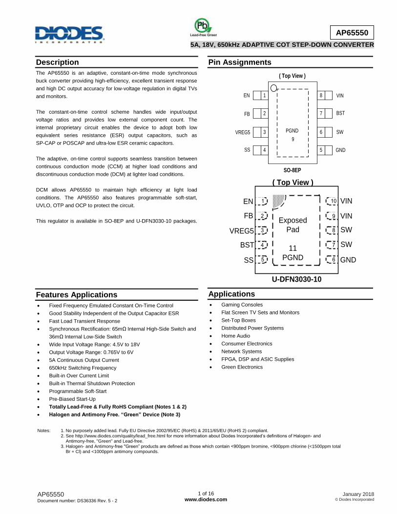
Pin Assignments
SWVREG5
SS
EN
BST
GND
VIN
( Top View )
1
2
3
4
8
7
6
5
FB
SO-8EP
PGND
9
Applications
Gaming Consoles
Flat Screen TV Sets and Monitors
Set-Top Boxes
Distributed Power Systems
Home Audio
Consumer Electronics
Network Systems
FPGA, DSP and ASIC Supplies
Green Electronics
Notes: 1. No purposely added lead. Fully EU Directive 2002/95/EC (RoHS) & 2011/65/EU (RoHS 2) compliant. 2. See http://www.diodes.com/quality/lead_free.html for more information about Diodes Incorporated’s definitions of Halogen- and Antimony-free, "Green" and Lead-free. 3. Halogen- and Antimony-free "Green” products are defined as those which contain <900ppm bromine, <900ppm chlorine (<1500ppm total Br + Cl) and <1000ppm antimony compounds.
EN 1 1 Enable input. EN is a digital input that turns the regulator on or off. Drive EN high to turn on the regulator, drive it low to turn off. Pull up with 100kΩ resistor to VIN for automatic startup.
FB 2 2 Feedback Input. FB senses the output voltage and regulates it. Drive FB with a resistive voltage divider connected to it from the output voltage.
VREG5 3 3 Internal power supply output pin to connect an additional capacitor. Connect a 1μF (typical) capacitor as close as possible to the VREG5 and PGND. This pin is not active when EN is low.
SS 4 5 Soft-start control input pin. SS controls the soft start period. Connect a capacitor from SS to GND to set the soft-start period.
GND 5 6 Ground pin is the main power ground for the switching circuit.
SW 6 7, 8 Power Switching Output. SW is the switching node that supplies power to the output. Connect the output LC filter from SW to the output load. Note that a capacitor is required from SW to BST to power the high-side switch.
BST 7 4 Bootstrap pin. A bootstrap capacitor is connected between the BST pin and SW pin. The voltage across the bootstrap capacitor drives the internal high-side NMOS switch. A 0.1μF (typical) capacitor is required for proper operation.
VIN 8 9, 10 Supply input pin. A capacitor should be connected between the VIN pin and PGND pin to keep the DC input voltage constant.
PGND 9
(Exposed Pad)
11
(Exposed Pad) Power ground. Exposed pad must be connected to a single point GND and as large of PGND plane as possible for maximum thermal performance.
Notes: 4. Stresses greater than the 'Absolute Maximum Ratings' specified above may cause permanent damage to the device. These are stress ratings only; functional operation of the device at these or any other conditions exceeding those indicated in this specification is not implied. Device reliability may be affected by exposure to absolute maximum rating conditions for extended periods of time.
5. Semiconductor devices are ESD sensitive and may be damaged by exposure to ESD events. Suitable ESD precautions should be taken when handling and transporting these devices.
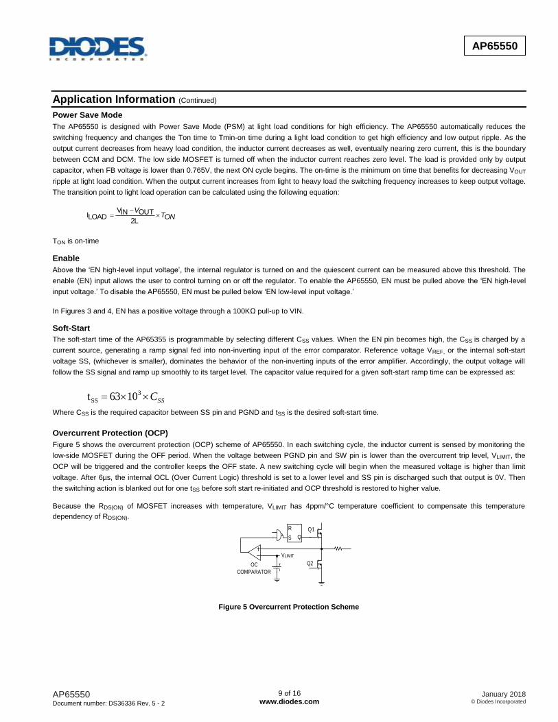
The AP65550 provides an undervoltage lockout circuit to prevent it from undefined status during startup. The UVLO circuit shuts down the device
when VIN drops below 3.45V. The UVLO circuit has 320mV hysteresis, which means the device starts up again when VREG rises to 3.75V (non-
latch).
Thermal shutdown
If the junction temperature of the device reaches the thermal shutdown limit of 160°C, the AP65550 shuts itself off, and both HS and LS
MOSFETs will be turned off. The output is discharged with the internal transistor. When the junction cools to the required level (+130°C nominal),
the device initiates soft-start as during a normal power-up cycle.
Power Derating Characteristics To prevent the regulator from exceeding the maximum junction temperature, some thermal analysis is required. The temperature rise is given by:
JAPD RISET
Where PD is the power dissipated by the regulator and JA is the thermal resistance from the junction of the die to the ambient temperature. The
junction temperature, TJ, is given by:
RISEA TT JT
TA is the ambient temperature of the environment. The actual junction temperature should not exceed the absolute maximum junction temperature of +125°C when considering the thermal design.
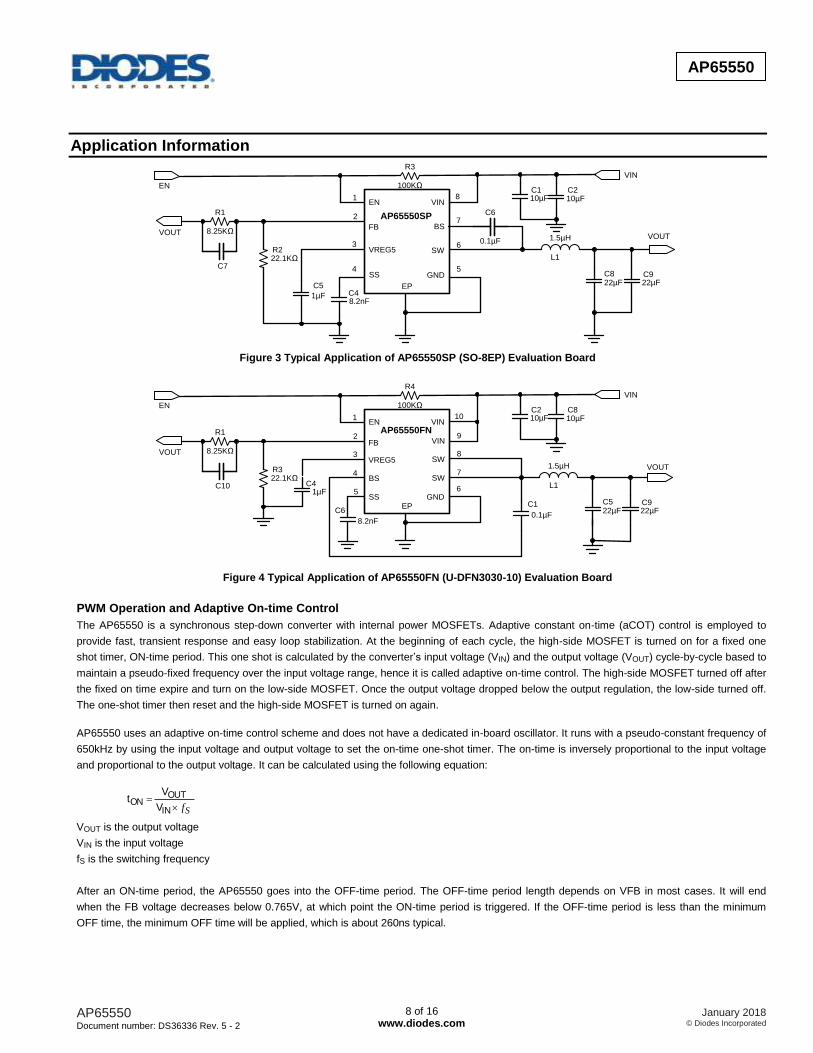
Setting the Output Voltage
The output voltage can be adjusted from 0.765 using an external resistor divider. Table 1 shows a list of resistor selection for common output
voltages. Resistor R1 is selected based on a design tradeoff between efficiency and output voltage accuracy. For high values of R1 there is less
current consumption in the feedback network. However the tradeoff is output voltage accuracy due to the bias current in the error amplifier. R1 can
be determined by the following equation:
1
0.765
OUTV2R1R
Inductor
Calculating the inductor value is a critical factor in designing a buck converter. For most designs, the following equation can be used to calculate
the inductor value:
SLIN
OUTINOUT
fΔIV
)V(VVL
Where IL is the inductor ripple current and fS is the switching frequency.
Choose the inductor ripple current to be 30% of the maximum load current. The maximum inductor peak current is calculated from:
2
ΔIII LLOADL(MAX)
Peak current determines the required saturation current rating, which influences the size of the inductor. Saturating the inductor decreases the
converter efficiency while increasing the temperatures of the inductor and the internal MOSFETs. Hence choosing an inductor with appropriate
saturation current rating is important.
Figure 6 Feedback Divider Network
Output Voltage (V) R1 (kΩ) R2 (kΩ)
1 6.81 22.1
1.05 8.25 22.1
1.2 12.7 22.1
1.5 21.5 22.1
1.8 30.1 22.1
2.5 49.9 22.1
3.3 73.2 22.1
5 124 22.1
Table 1 Resistor Selection for Common Output Voltages
A 1µH to 3.3µH inductor with a DC current rating of at least 25% percent higher than the maximum load current is recommended for most
applications. For highest efficiency, the inductor’s DC resistance should be less than 100mΩ. Use a larger inductance for improved efficiency
under light load conditions. The phase boost can be achieved by adding an additional feed forward capacitor (C7) parallel to R1.
Output Voltage (V) C7(pF) L1(µH) C8+C9(µF)
1 — 1.0-1.5 22-68
1.05 — 1.0-1.5 22-68
1.2 — 1.0-1.5 22-68
1.5 — 1.5 22-68
1.8 5-22 1.5 22-68
2.5 5-22 2.2 22-68
3.3 5-22 2.2 22-68
5 5-22 3.3 22-68
Table 2 Recommended Component Selection
Input Capacitor
The input capacitor reduces the surge current drawn from the input supply and the switching noise from the device. The input capacitor has to
sustain the ripple current produced during the on time on the upper MOSFET. It must have a low ESR to minimize the losses.
The RMS current rating of the input capacitor is a critical parameter that must be higher than the RMS input current. As a rule of thumb, select an
input capacitor which has an RMs rating greater than half of the maximum load current.
Due to large dI/dt through the input capacitors, electrolytic or ceramics should be used. If a tantalum must be used it must be surge protected,
otherwise, capacitor failure could occur. For most applications greater than 10µF, ceramic capacitor is sufficient.
Output Capacitor
The output capacitor keeps the output voltage ripple small, ensures feedback loop stability and reduces the overshoot of the output voltage. The
output capacitor is a basic component for the fast response of the power supply. In fact, during load transient, for the first few microseconds it
supplies the current to the load. The converter recognizes the load transient and sets the duty cycle to maximum, but the current slope is limited
by the inductor value. Maximum capacitance required can be calculated from the following equation:
ESR of the output capacitor dominates the output voltage ripple. The amount of ripple can be calculated from the equation below:
ESR*ΔIV INDUCTOROUT_RIPPLE
An output capacitor with ample capacitance and low ESR is the best option. For most applications, a 22µF to 68µF ceramic capacitor will be sufficient.
2OUT
2OUT
2INDUCTOROUT
OV)V V(Δ
)2
ΔIL(I
C
Where ΔV is the maximum output voltage overshoot.
Bootstrap Capacitor To ensure the proper operation, a ceramic capacitor must be connected between the VBST and SW pin. A 0.1µF ceramic capacitor is sufficient.
VREG5 Capacitor To ensure the proper operation, a ceramic capacitor must be connected between the VREG5 and PGND pin. A 1µF ceramic capacitor is sufficient.
IMPORTANT NOTICE DIODES INCORPORATED MAKES NO WARRANTY OF ANY KIND, EXPRESS OR IMPLIED, WITH REGARDS TO THIS DOCUMENT, INCLUDING, BUT NOT LIMITED TO, THE IMPLIED WARRANTIES OF MERCHANTABILITY AND FITNESS FOR A PARTICULAR PURPOSE (AND THEIR EQUIVALENTS UNDER THE LAWS OF ANY JURISDICTION). Diodes Incorporated and its subsidiaries reserve the right to make modifications, enhancements, improvements, corrections or other changes without further notice to this document and any product described herein. Diodes Incorporated does not assume any liability arising out of the application or use of this document or any product described herein; neither does Diodes Incorporated convey any license under its patent or trademark rights, nor the rights of others. Any Customer or user of this document or products described herein in such applications shall assume all risks of such use and will agree to hold Diodes Incorporated and all the companies whose products are represented on Diodes Incorporated website, harmless against all damages. Diodes Incorporated does not warrant or accept any liability whatsoever in respect of any products purchased through unauthorized sales channel. Should Customers purchase or use Diodes Incorporated products for any unintended or unauthorized application, Customers shall indemnify and hold Diodes Incorporated and its representatives harmless against all claims, damages, expenses, and attorney fees arising out of, directly or indirectly, any claim of personal injury or death associated with such unintended or unauthorized application. Products described herein may be covered by one or more United States, international or foreign patents pending. Product names and markings noted herein may also be covered by one or more United States, international or foreign trademarks. This document is written in English but may be translated into multiple languages for reference. Only the English version of this document is the final and determinative format released by Diodes Incorporated.
LIFE SUPPORT Diodes Incorporated products are specifically not authorized for use as critical components in life support devices or systems without the express written approval of the Chief Executive Officer of Diodes Incorporated. As used herein: A. Life support devices or systems are devices or systems which: 1. are intended to implant into the body, or
2. support or sustain life and whose failure to perform when properly used in accordance with instructions for use provided in the labeling can be reasonably expected to result in significant injury to the user.