Page 1
External Use
Enabling the Semiconductor
Roadmap from a Multi-Angled
Approach
June 13th, 2019
Steven Welch
Senior Director of Strategy, Advanced Product and Technology
Development, Applied Materials
Page 2
External Use
Steven Welch is currently Senior Director of Strategy for Applied
Materials’ Advanced Product and Technology Development
group. In this role, he is responsible for identifying and synthesizing
key inflections in the longer-term Semiconductor technology
roadmap, as well as enabling disruptive technology development
and business growth strategies to intercept these emerging
opportunities. With over 20 years in the industry, Steven started his
career in 1998 as a photolithography engineer at IBM’s Storage
Systems Division in San Jose, California. Since then, he has held
marketing and strategy leadership positions in KLA-Tencor’s wafer
inspection, Applied Materials’ etch, and ASML’s holistic lithography
businesses. Steven holds a B.S. in Chemistry from Harvey Mudd
College and MA & MBA degrees from the University of
Pennsylvania’s Wharton School of Business.
2
Introduction
Page 3
External Use3
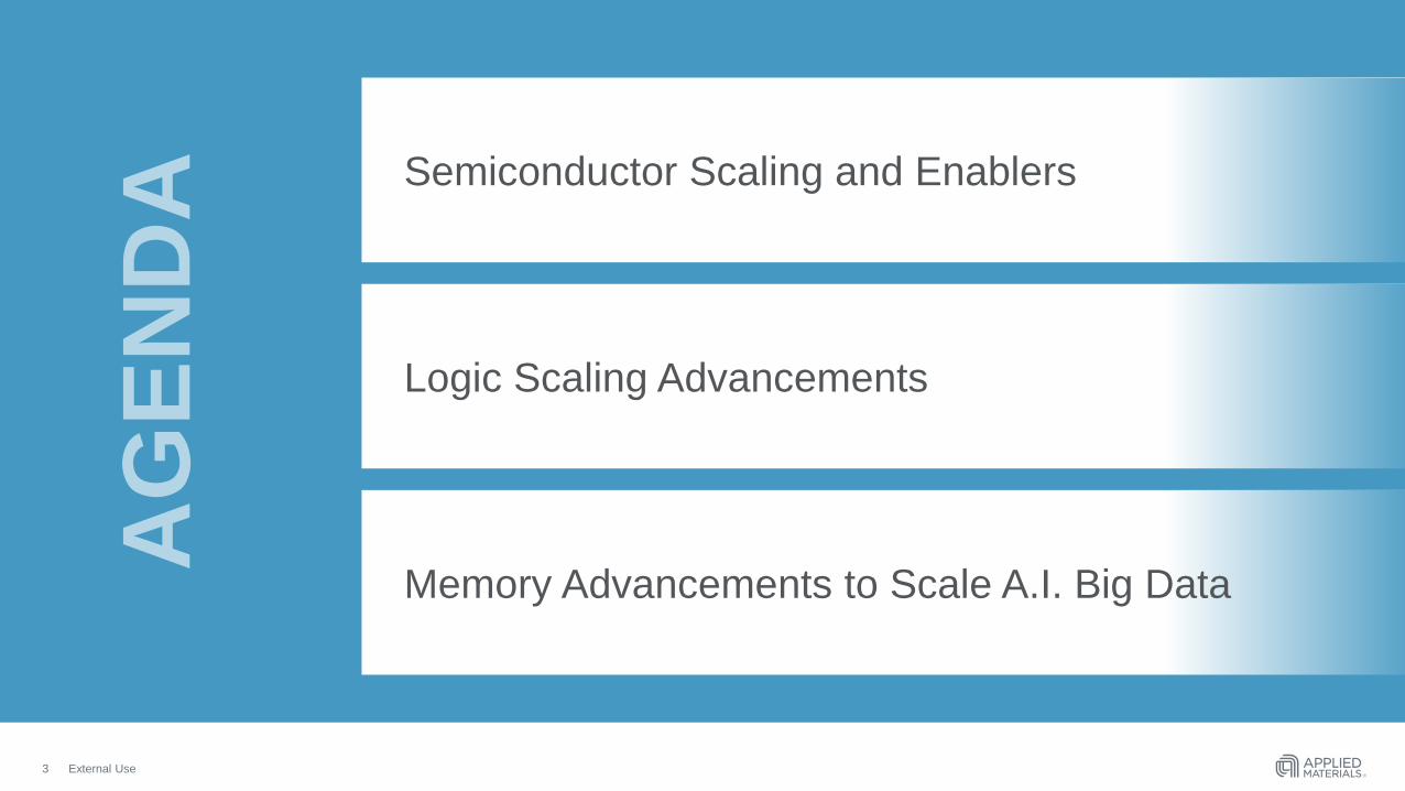
Semiconductor Scaling and Enablers
Logic Scaling Advancements
Memory Advancements to Scale A.I. Big Data
AG
EN
DA
Page 4
External Use4
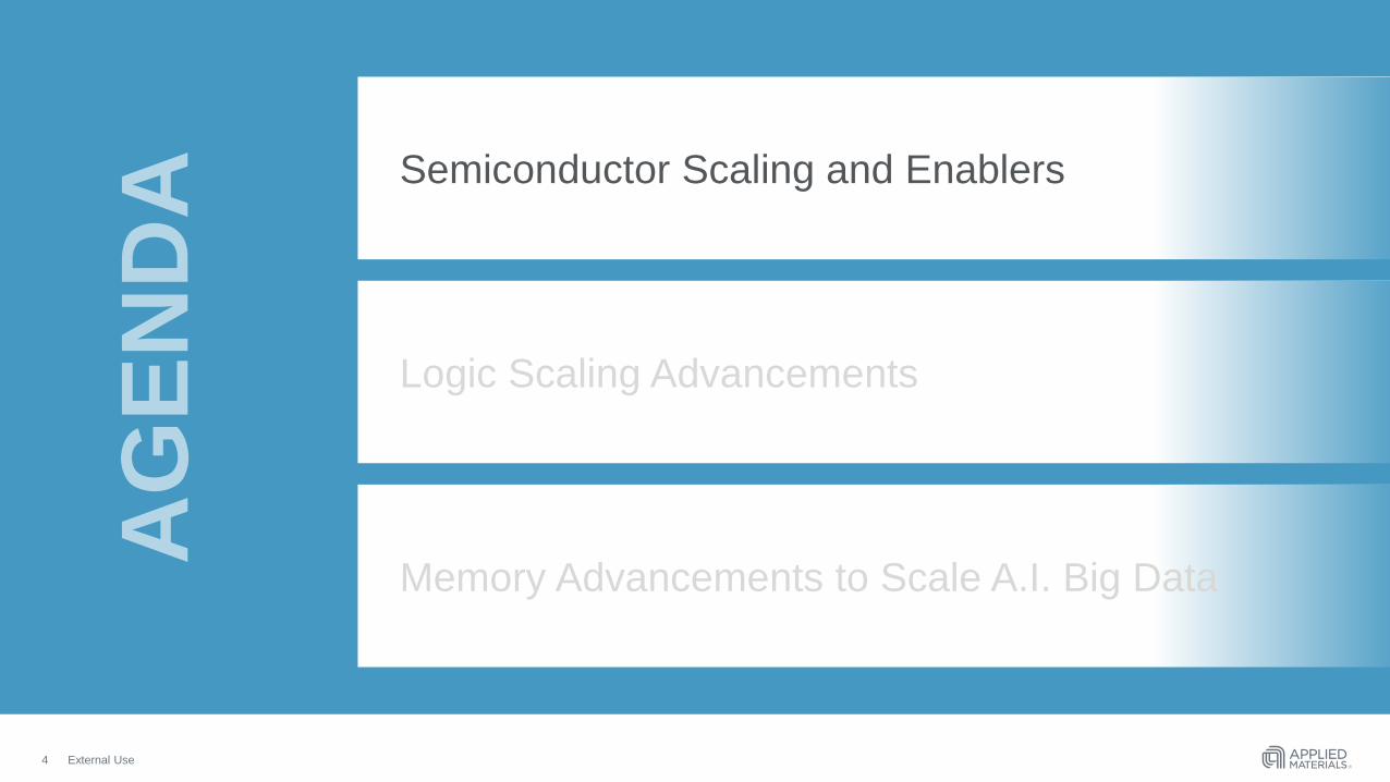
Semiconductor Scaling and Enablers
Logic Scaling Advancements
Memory Advancements to Scale A.I. Big Data
AG
EN
DA
Page 5
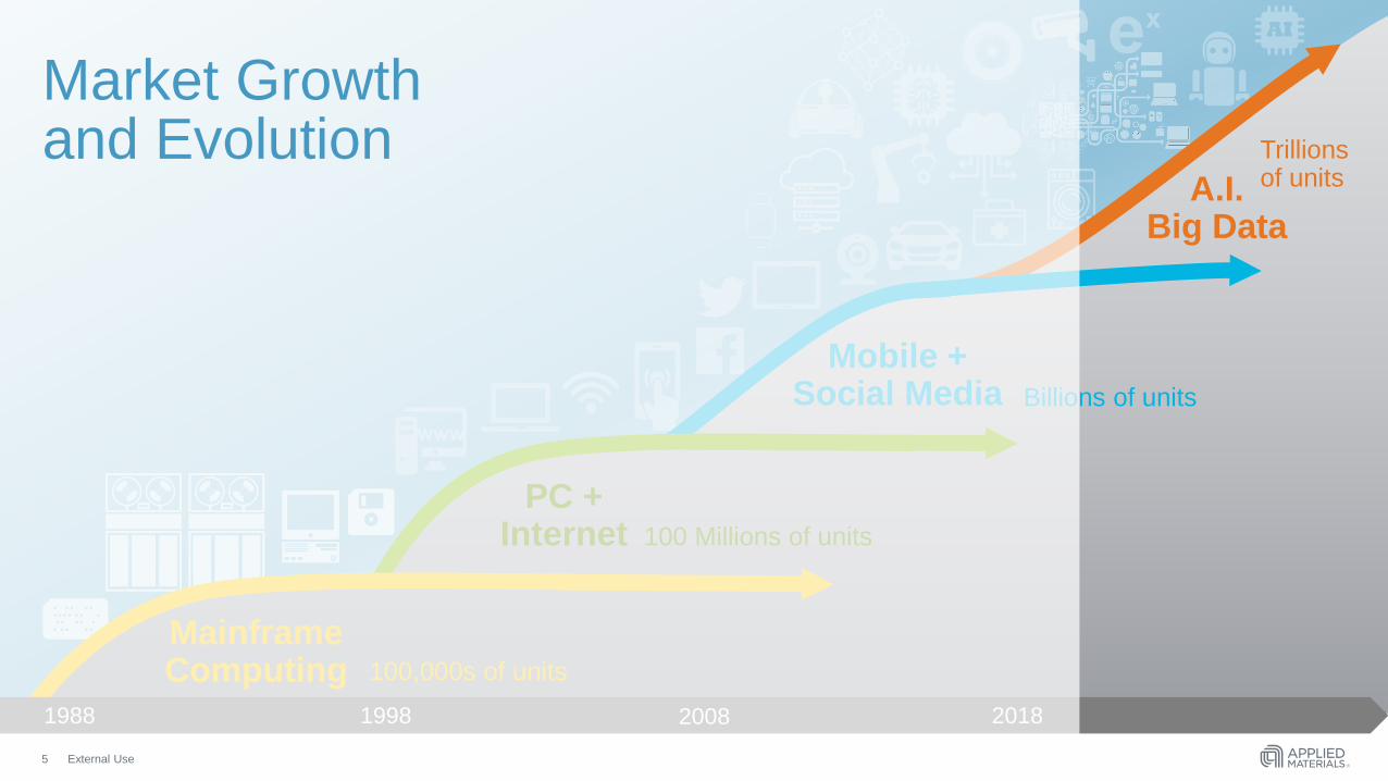
External Use5
PC + Internet
Mobile +Social Media
A.I. Big Data
Mainframe Computing 100,000s of units
100 Millions of units
Billions of units
Trillions of units
1998 2008 20181988
Market Growth and Evolution
Page 6
External Use
105
104
103
102
10
1
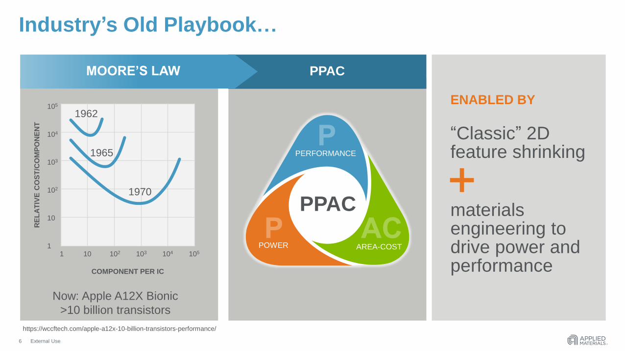
Industry’s Old Playbook…
COMPONENT PER IC
RE
LA
TIV
E C
OS
T/C
OM
PO
NE
NT
1 10 102 103 104 105
1962
1965
1970
PPAC
“Classic” 2D feature shrinking
materials engineering to drive power and performance
ENABLED BY
PPAC
POWER
PERFORMANCE
AREA-COST
MOORE’S LAW
6
Now: Apple A12X Bionic
>10 billion transistors
https://wccftech.com/apple-a12x-10-billion-transistors-performance/
Page 7
External Use
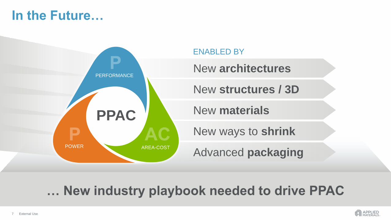
In the Future…
ENABLED BY
Advanced packaging
New structures / 3D
New ways to shrink
New architectures
New materialsPPAC
POWER
PERFORMANCE
AREA-COST
… New industry playbook needed to drive PPAC
7
Page 8
External Use8
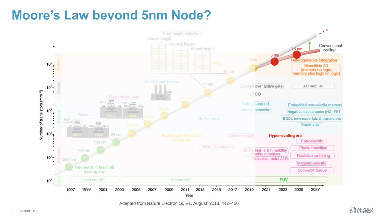
Adapted from Nature Electronics, V1, August’ 2018, 442–450
Moore’s Law beyond 5nm Node?
Negative capacitance (NC)-FET
AI compute
BEOL new materials & transistors3D Memories
Page 9
External Use9
Semiconductor Scaling and Enablers
Logic Scaling Advancements
Memory Advancements to Scale A.I. Big Data
AG
EN
DA
Page 10
External Use
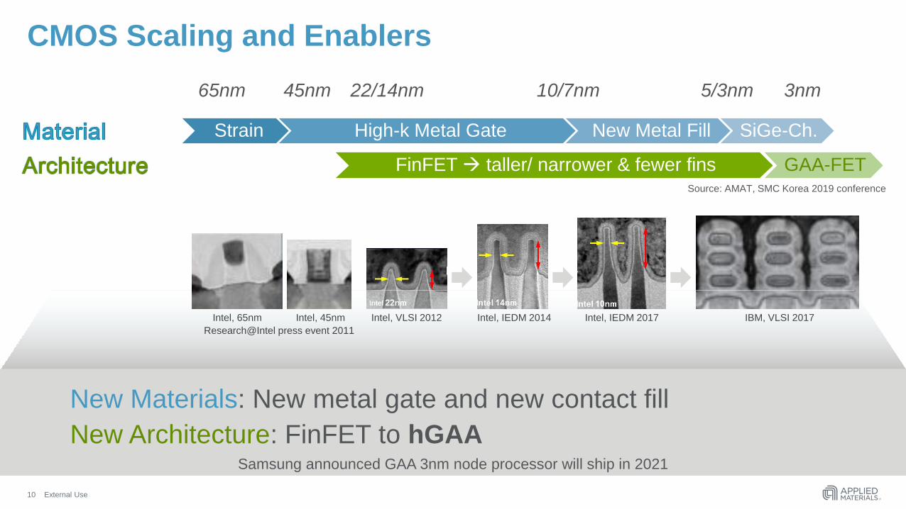
CMOS Scaling and Enablers
10
Strain High-k Metal Gate New Metal Fill SiGe-Ch.
FinFET taller/ narrower & fewer fins GAA-FET
10/7nm 3nm5/3nm22/14nm65nm 45nm
New Materials: New metal gate and new contact fill
New Architecture: FinFET to hGAA
Intel, VLSI 2012 Intel, IEDM 2014 Intel, IEDM 2017 IBM, VLSI 2017Intel, 65nm Intel, 45nm
Samsung announced GAA 3nm node processor will ship in 2021
Source: AMAT, SMC Korea 2019 conference
Research@Intel press event 2011
Page 11
External Use11
Why Horizontal-GAA Evolutional Change
xFin
Thinner & Taller Fins better gate control & higher drive current
SiGe p-Channel mobility boosting
FinFET
Vertically stackable channel (NW/NS) for increased current per area
Similar structures & flows: hGAA vs. FinFET
hGAA
G
G
G
G
xNW
Intel, IEDM 2017 IBM, VLSI 2017GLOBALFOUNDRIES/IBM, IEDM 2016
Page 12
External Use12
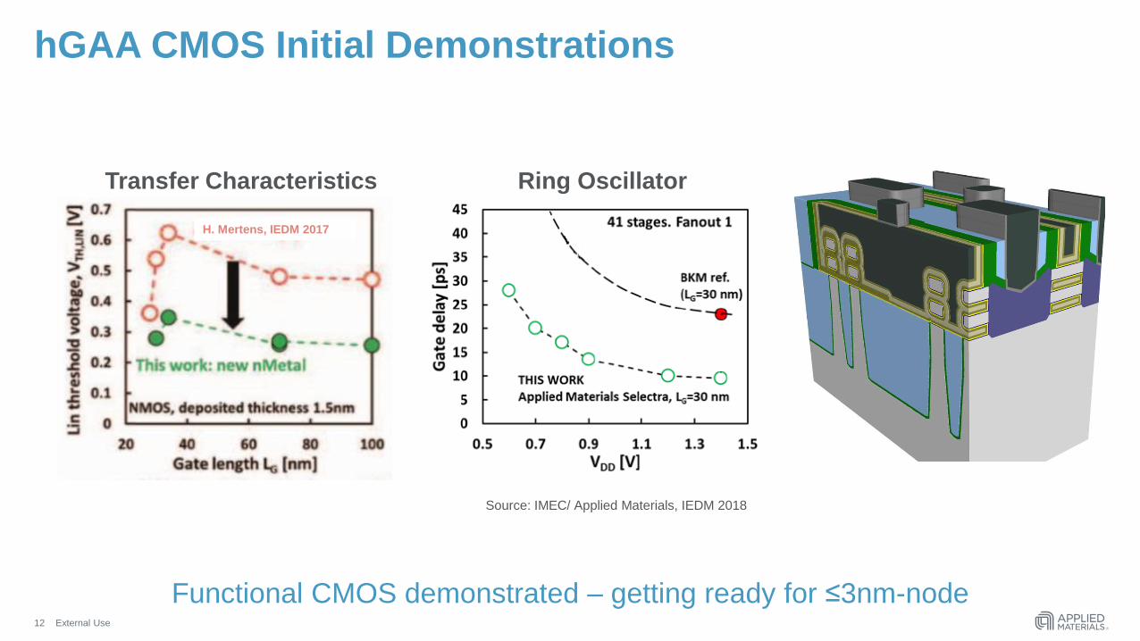
hGAA CMOS Initial Demonstrations
Transfer Characteristics Ring Oscillator
Source: IMEC/ Applied Materials, IEDM 2018
Functional CMOS demonstrated – getting ready for ≤3nm-node
H. Mertens, IEDM 2017
Page 13
External Use13
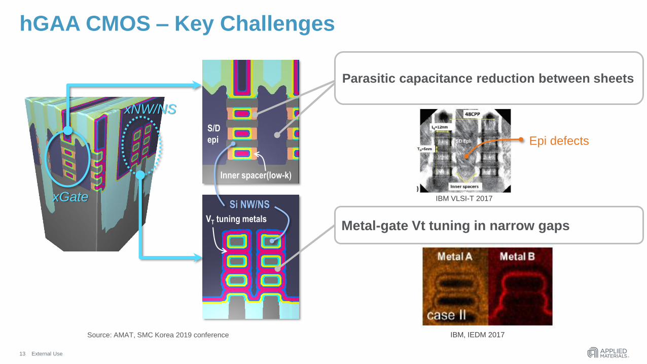
hGAA CMOS – Key Challenges
S/D
epi
Inner spacer(low-k)
VT tuning metals
Si NW/NSxGate
xNW/NS
Parasitic capacitance reduction between sheets
Metal-gate Vt tuning in narrow gaps
IBM, IEDM 2017
Epi defects
IBM VLSI-T 2017
Source: AMAT, SMC Korea 2019 conference
Page 14
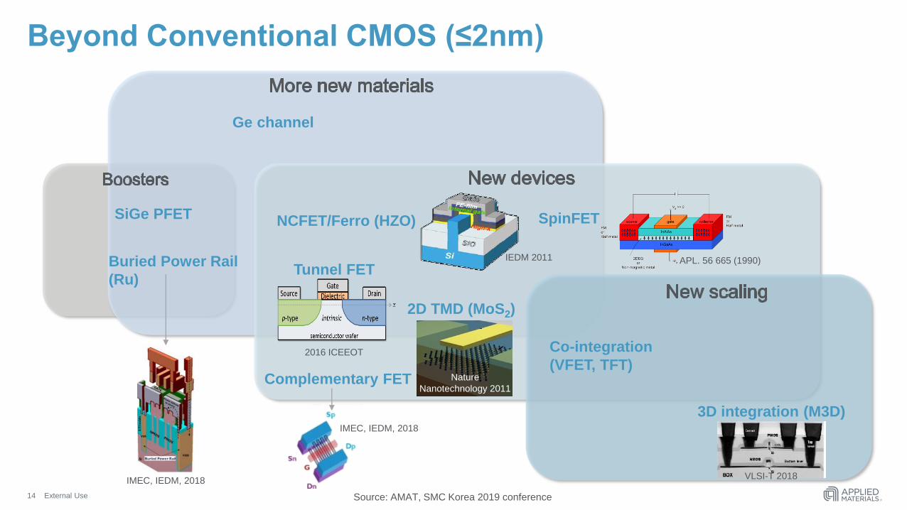
External Use14
Beyond Conventional CMOS (≤2nm)
Source: AMAT, SMC Korea 2019 conference
Ge channel
NCFET/Ferro (HZO)
2D TMD (MoS2)
3D integration (M3D)
Co-integration
(VFET, TFT)Complementary FET
SiGe PFET
Buried Power Rail
(Ru)Tunnel FET
VLSI-T 2018
Nature
Nanotechnology 2011
IEDM 2011
SpinFET
APL. 56 665 (1990)
IMEC, IEDM, 2018
2016 ICEEOT
IMEC, IEDM, 2018
Page 15
External Use15
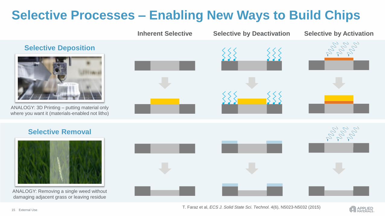
Selective Processes – Enabling New Ways to Build Chips
Selective Removal
ANALOGY: Removing a single weed without
damaging adjacent grass or leaving residue
Selective Deposition
ANALOGY: 3D Printing – putting material only
where you want it (materials-enabled not litho)
T. Faraz et al, ECS J. Solid State Sci. Technol. 4(6), N5023-N5032 (2015)
Inherent Selective Selective by Deactivation Selective by Activation
Page 16
External Use16
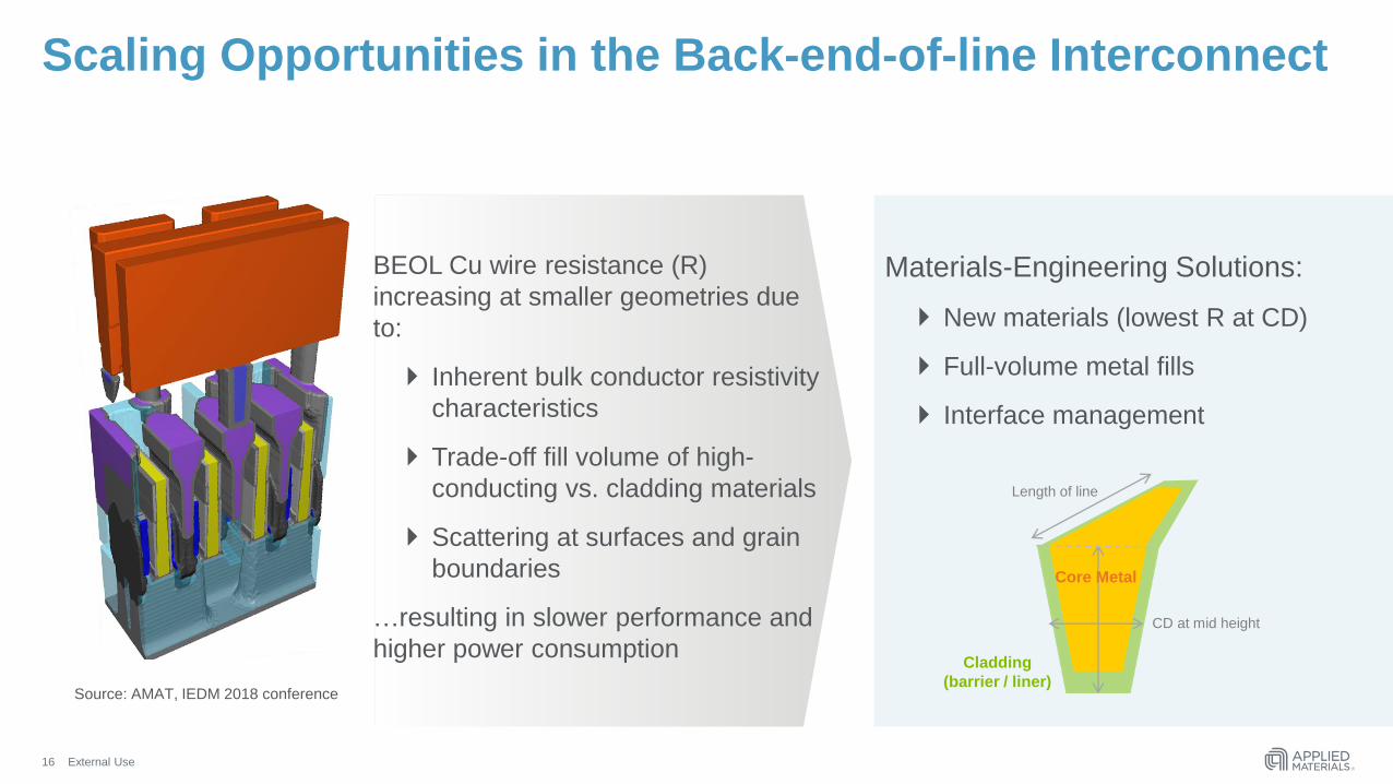
Scaling Opportunities in the Back-end-of-line Interconnect
BEOL Cu wire resistance (R)
increasing at smaller geometries due
to:
Inherent bulk conductor resistivity
characteristics
Trade-off fill volume of high-
conducting vs. cladding materials
Scattering at surfaces and grain
boundaries
…resulting in slower performance and
higher power consumption
Source: AMAT, IEDM 2018 conference
Materials-Engineering Solutions:
New materials (lowest R at CD)
Full-volume metal fills
Interface management
Length of line
CD at mid height
Core Metal
Cladding
(barrier / liner)
Page 17
External Use17
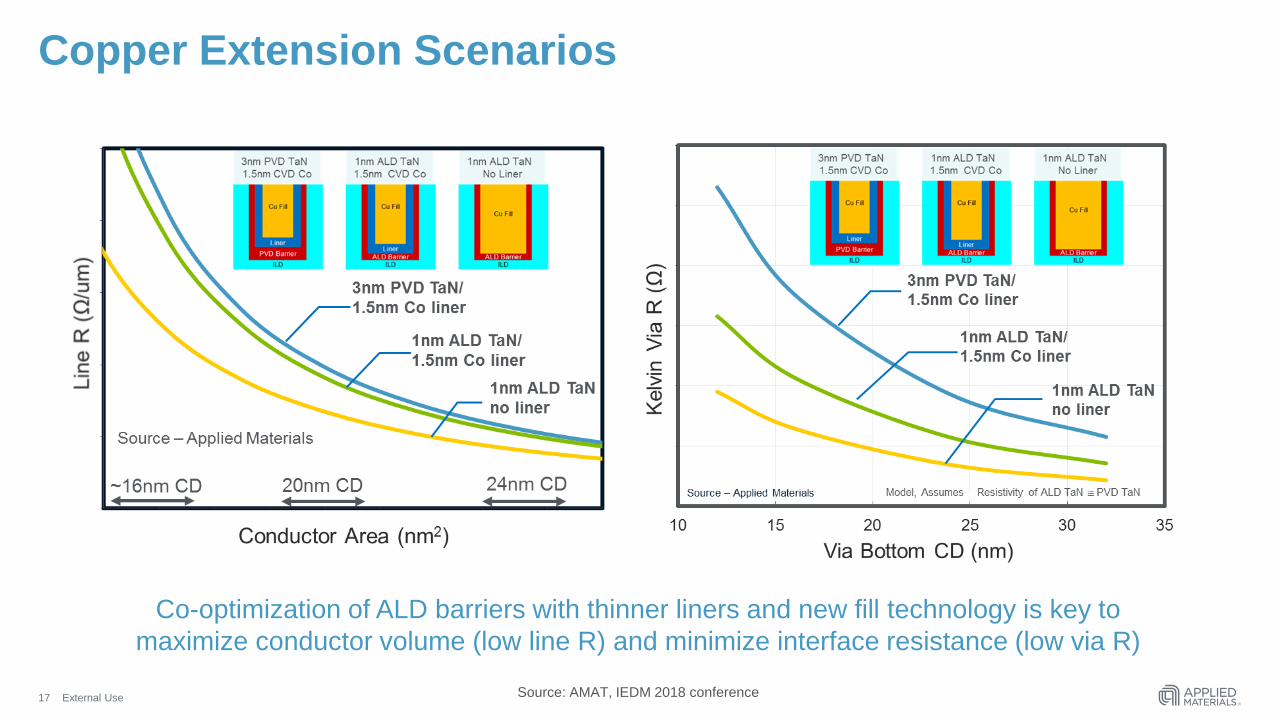
Copper Extension Scenarios
Co-optimization of ALD barriers with thinner liners and new fill technology is key to
maximize conductor volume (low line R) and minimize interface resistance (low via R)
Source: AMAT, IEDM 2018 conference
Page 18
External Use18
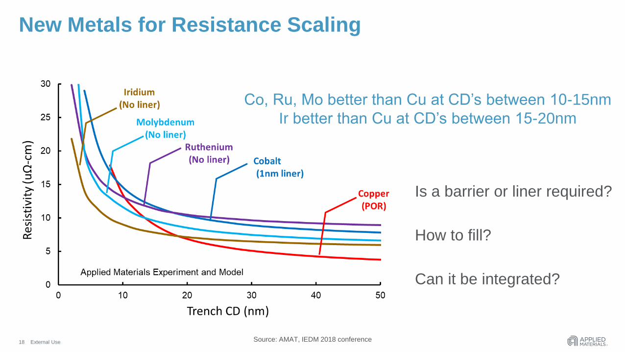
New Metals for Resistance Scaling
Co, Ru, Mo better than Cu at CD’s between 10-15nm
Ir better than Cu at CD’s between 15-20nm
Is a barrier or liner required?
How to fill?
Can it be integrated?
Source: AMAT, IEDM 2018 conference
Page 19
External Use19
Semiconductor Scaling and Enablers
Logic Scaling Advancements
Memory Advancements to Scale A.I. Big Data
AG
EN
DA
Page 20
External Use
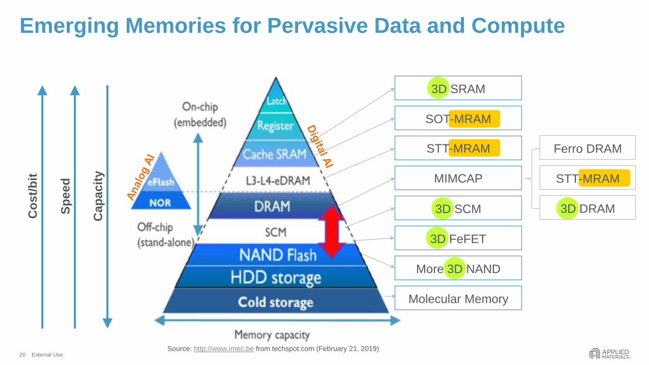
Emerging Memories for Pervasive Data and Compute
20
Co
st/
bit
Sp
eed
Cap
acit
y
Source: http://www.imec.be from techspot.com (February 21, 2019)
Ferro DRAM
STT-MRAM
3D DRAM
3D SRAM
SOT-MRAM
STT-MRAM
MIMCAP
3D SCM
3D FeFET
More 3D NAND
Molecular Memory
Page 21
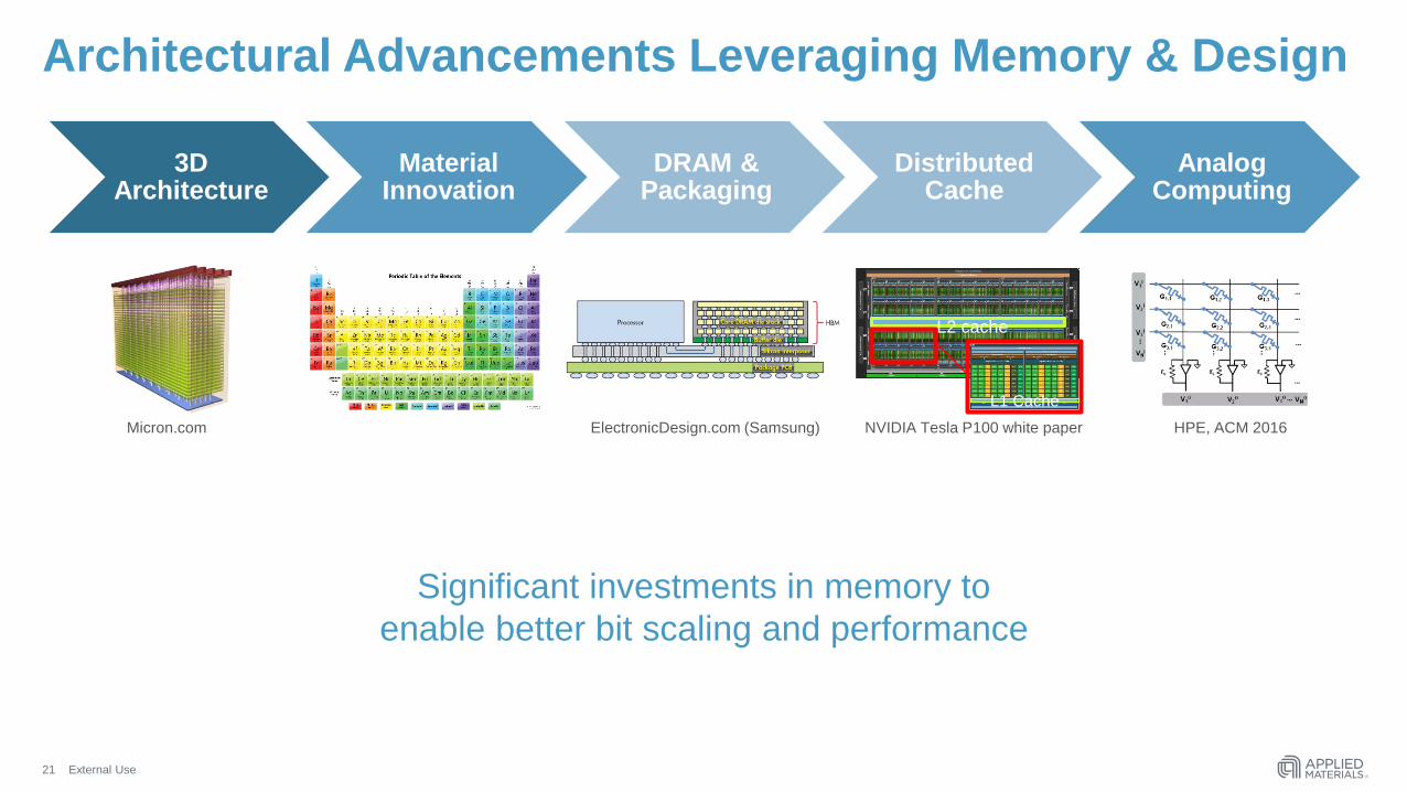
External Use
Architectural Advancements Leveraging Memory & Design
21
3D Architecture
Material Innovation
DRAM & Packaging
Distributed Cache
Analog Computing
NVIDIAL2 cache
L1 Cache
HPE, ACM 2016 NVIDIA Tesla P100 white paperMicron.com
Significant investments in memory to
enable better bit scaling and performance
ElectronicDesign.com (Samsung)
Page 22
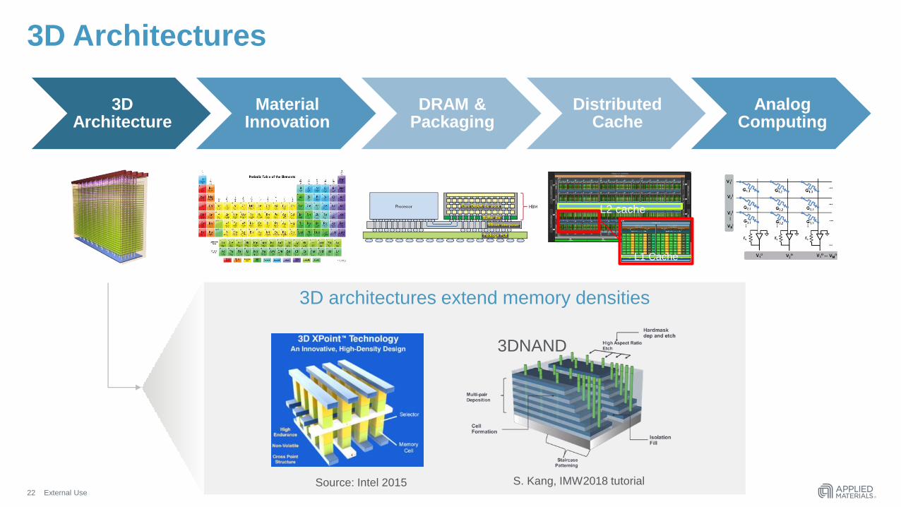
External Use
3D Architectures
22
3D Architecture
Material Innovation
DRAM & Packaging
Distributed Cache
Analog Computing
NVIDIAL2 cache
L1 Cache
3D architectures extend memory densities
Source: Intel 2015 S. Kang, IMW2018 tutorial
3DNAND
Page 23
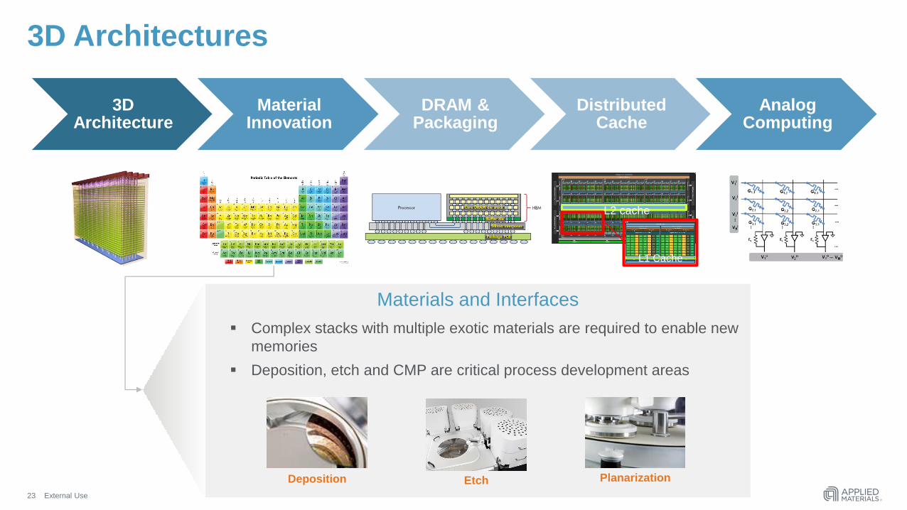
External Use
3D Architectures
23
3D Architecture
Material Innovation
DRAM & Packaging
Distributed Cache
Analog Computing
NVIDIAL2 cache
L1 Cache
Materials and Interfaces
▪ Complex stacks with multiple exotic materials are required to enable new
memories
▪ Deposition, etch and CMP are critical process development areas
Deposition PlanarizationEtch
Page 24
External Use24
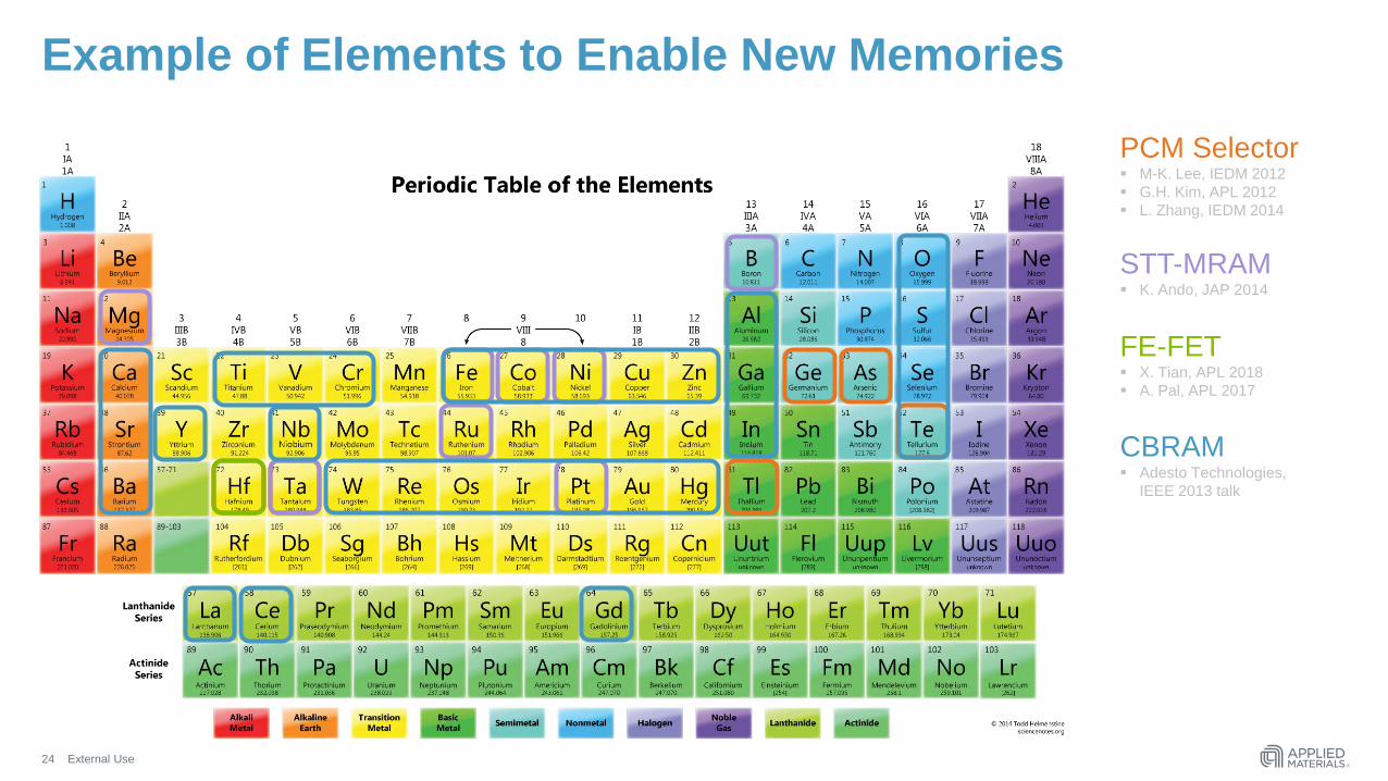
Example of Elements to Enable New Memories
PCM Selector▪ M-K. Lee, IEDM 2012
▪ G.H. Kim, APL 2012
▪ L. Zhang, IEDM 2014
STT-MRAM▪ K. Ando, JAP 2014
FE-FET▪ X. Tian, APL 2018
▪ A. Pal, APL 2017
CBRAM▪ Adesto Technologies,
IEEE 2013 talk
Page 25
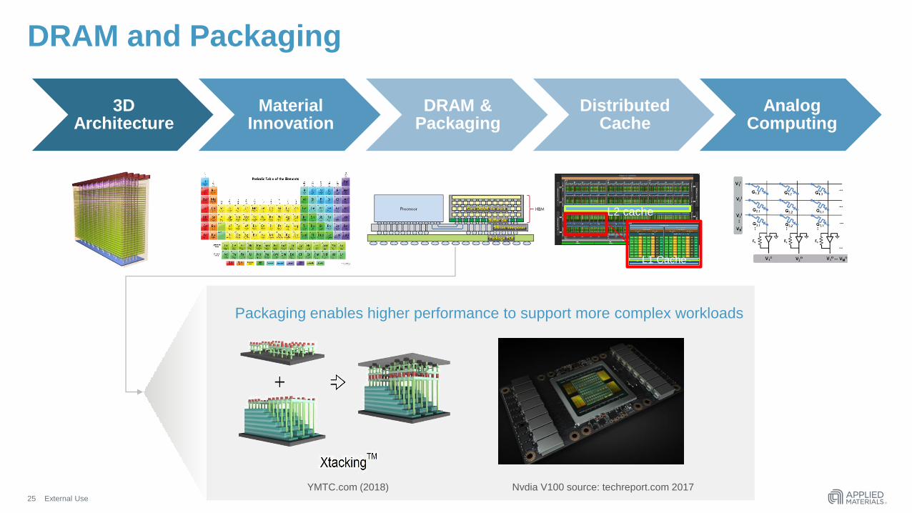
External Use
DRAM and Packaging
25
3D Architecture
Material Innovation
DRAM & Packaging
Distributed Cache
Analog Computing
NVIDIAL2 cache
L1 Cache
Packaging enables higher performance to support more complex workloads
Nvdia V100 source: techreport.com 2017YMTC.com (2018)
Page 26
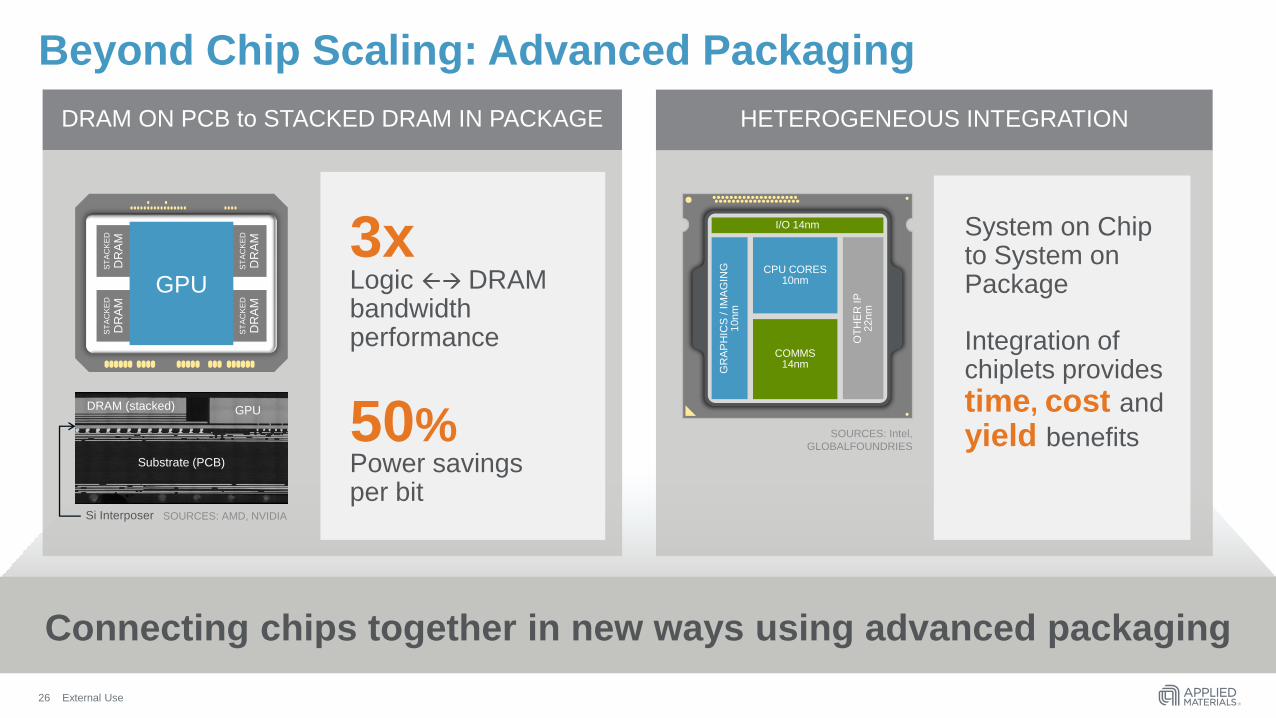
External Use
DRAM ON PCB to STACKED DRAM IN PACKAGE HETEROGENEOUS INTEGRATION
System on Chip to System on Package
Integration of chiplets provides
time, cost and
yield benefits
GR
AP
HIC
S / IM
AG
ING
10nm
OT
HE
R IP
22nm
CPU CORES10nm
COMMS14nm
I/O 14nm
Power savings per bit
3x
50%
Logic DRAM bandwidth performance
Substrate (PCB)
DRAM (stacked) GPU
Si Interposer
SOURCES: Intel,
GLOBALFOUNDRIES
SOURCES: AMD, NVIDIA
ST
AC
KE
D
DR
AM
ST
AC
KE
D
DR
AM
ST
AC
KE
D
DR
AM
ST
AC
KE
D
DR
AM
GPU
Beyond Chip Scaling: Advanced Packaging
Connecting chips together in new ways using advanced packaging
26
Page 27
External Use
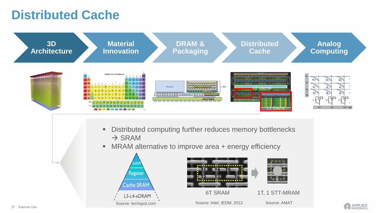
Distributed Cache
27
3D Architecture
Material Innovation
DRAM & Packaging
Distributed Cache
Analog Computing
NVIDIAL2 cache
L1 Cache
▪ Distributed computing further reduces memory bottlenecks
SRAM
▪ MRAM alternative to improve area + energy efficiency
1T, 1 STT-MRAM 6T SRAM
Source: techspot.com Source: Intel, IEDM, 2012 Source: AMAT
Page 28
External Use28
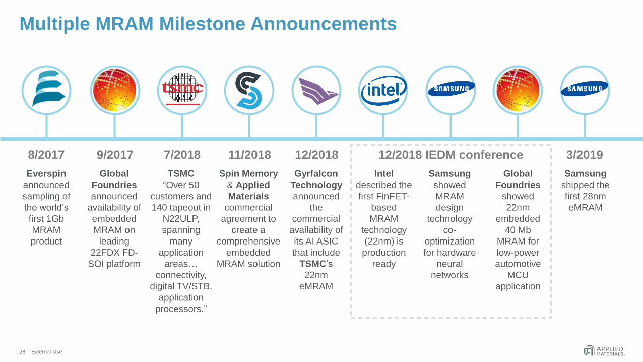
Multiple MRAM Milestone Announcements
8/2017 3/20197/20189/2017 11/2018 12/2018
Everspin
announced
sampling of
the world’s
first 1Gb
MRAM
product
Samsung
shipped the
first 28nm
eMRAM
Global
Foundries
announced
availability of
embedded
MRAM on
leading
22FDX FD-
SOI platform
TSMC
“Over 50
customers and
140 tapeout in
N22ULP,
spanning
many
application
areas…
connectivity,
digital TV/STB,
application
processors.”
Spin Memory
& Applied
Materials
commercial
agreement to
create a
comprehensive
embedded
MRAM solution
Gyrfalcon
Technology
announced
the
commercial
availability of
its AI ASIC
that include
TSMC’s
22nm
eMRAM
Intel
described the
first FinFET-
based
MRAM
technology
(22nm) is
production
ready
Samsung
showed
MRAM
design
technology
co-
optimization
for hardware
neural
networks
Global
Foundries
showed
22nm
embedded
40 Mb
MRAM for
low-power
automotive
MCU
application
12/2018 IEDM conference
Page 29
External Use
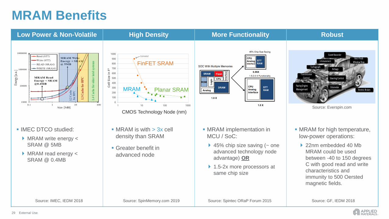
Low Power & Non-Volatile High Density More Functionality Robust
MRAM Benefits
29
▪ IMEC DTCO studied:
MRAM write energy <
SRAM @ 5MB
MRAM read energy <
SRAM @ 0.4MB
▪ MRAM is with > 3x cell
density than SRAM
▪ Greater benefit in
advanced node
Source: SpinMemory.com 2019Source: IMEC, IEDM 2018 Source: Spintec ORaP Forum 2015
CMOS Technology Node (nm)
FinFET SRAM
MRAM Planar SRAM
▪ MRAM implementation in
MCU / SoC:
45% chip size saving (~ one
advanced technology node
advantage) OR
1.5-2x more processors at
same chip size
Source: GF, IEDM 2018
▪ MRAM for high temperature,
low-power operations:
22nm embedded 40 Mb
MRAM could be used
between -40 to 150 degrees
C with good read and write
characteristics and
immunity to 500 Oersted
magnetic fields.
Source: Everspin.com
Page 30
External Use
MRAM Capability Demonstrated by Optimization of Complex Stack
Roadmap for additional density and performance scaling in development
Sources: Applied Materials
IEDM, 2015
IEDM, 2016
VLSI, 2018
VLSI, 2018
30
Page 31
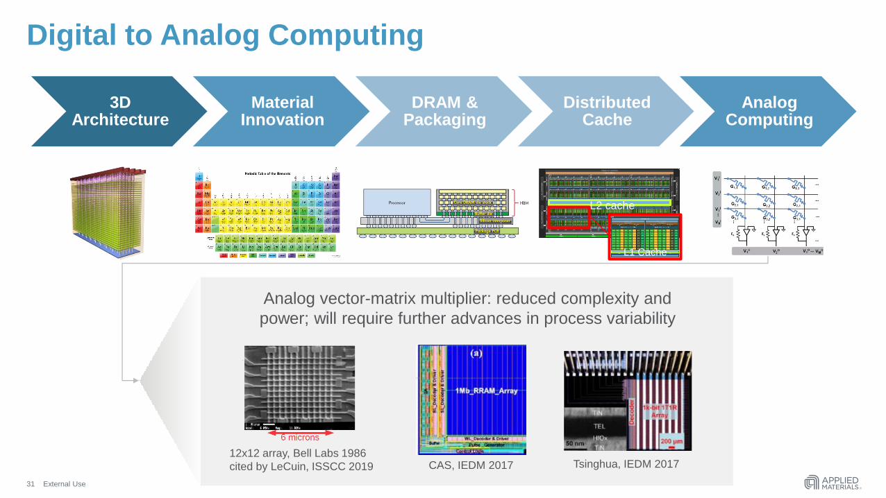
External Use
Digital to Analog Computing
31
3D Architecture
Material Innovation
DRAM & Packaging
Distributed Cache
Analog Computing
NVIDIAL2 cache
L1 Cache
Analog vector-matrix multiplier: reduced complexity and
power; will require further advances in process variability
CAS, IEDM 2017 Tsinghua, IEDM 201712x12 array, Bell Labs 1986
cited by LeCuin, ISSCC 2019
Page 32
External Use
Emerging Memory for Machine Learning Accelerators
1. Digital Accelerator
“The 2802M ASIC has 40MB of
eMRAM memory, which can
support large AI models or
multiple AI models within a
single chip.” – gyrfalcontech.ai
2019
▪ New analog memories, once performance at scale is
robust, can enable additional performance boosts @
density and new ways of compute
2. Analog Accelerator
Weights: Conductance of NVM
Matrix multiplication in hardware
(Ohms, Kirchhoff law)
NVM
“1,000 to 10,000 better speed-energy efficiency product
than digital ASICs” - HPE, ACM 2016
▪ MRAM can enable area benefit at lower power versus
traditional distributed SRAM techniques
SRAM → MRAM available in Foundry eFlash → RERAM, FEFET, PCRAM in Development
32
In-memory Compute Vector-Matrix Multiplier
Page 33
External Use
PPAC Optimization Beyond the Chip
33 Image sources: Applied Materials Blog