Page 1
Energy-Efficient Spin-Transfer Torque RAM Cache
Exploiting Additional All-Zero-Data Flags
Jinwook Jung†, Yohei Nakata, Masahiko Yoshimoto, and Hiroshi Kawaguchi
Graduate School of System Informatics, Kobe University, Japan †E-mail: [email protected]
Abstract Large on-chip caches account for a considerable fraction
of the total energy consumption in modern microprocessors.
In this context, emerging Spin-Transfer Torque RAM (STT-
RAM) has been regarded as a promising candidate to replace
large on-chip SRAM caches in virtue of its nature of the zero
leakage. However, large energy requirement of STT-RAM
on write operations, resulting in a huge amount of dynamic
energy consumption, precludes it from application to on-chip
cache designs. In order to reduce the write energy of the
STT-RAM cache thereby the total energy consumption, this
paper provides an architectural technique which exploits the
fact that many applications process a large number of zero
data. The proposed design appends additional flags in cache
tag arrays and set these additional bits if the corresponding
data in the cache line is the zero-valued data in which all
data bits are zero. Our experimental results show that the
proposed cache design can reduce 73.78% and 69.30% of
the dynamic energy on write operations at the byte and word
granularities, respectively; total energy consumption reduced
by 36.18% and 42.51%, respectively. In addition to the
energy reduction, performance evaluation results indicate
that the proposed cache improves the processor performance
by 5.44% on average.
Keywords Cache, Emerging devices, Spin-Transfer Torque RAM,
Energy consumption, Zero-valued data
1. Introduction With the advancement of the technology scaling, energy
dissipation has come to be an increasingly significant
challenges in integrated circuit designs [1]. In modern
microprocessors, large on-chip caches which occupy a great
fraction of the entire transistor counter account for a large
portion of overall energy dissipation as well [2]–[3]. These
cache structures are traditionally implemented with SRAM
cells because of its fast access time. However, as the feature
size of the process technology continues to scale down, the
exponential increase of leakage power makes the SRAM-
based on-chip cache a bottleneck of energy-efficient design
[4]–[5].
Emerging non-volatile memory technologies have drawn
attention as promising candidates to reduce the large energy
consumption in the SRAM due to their inherent nature of
nearly zero stand-by leakage. Among non-volatile memories,
Spin-Transfer Torque RAM (STT-RAM) offers a faster read
speed, higher integration density and better CMOS
compatibility as well as virtually infinite write endurance [6].
By virtue of these advantages, STT-RAM has been thought
of as a promising alternative to SRAM in large on-chip
caches such as Level-two cache (L2 cache) and last level
cache (LLC) [7]–[10].
However, in spite of these benefits of STT-RAM, one of
the most significant challenges is its high energy on write
operations. STT-RAM requires a substantial amount of
current through a magnetic tunnel junction (MTJ), its
memory element, during the write operations. This drawback
hinders the substitution of SRAM for STT-RAM in on-chip
cache structures for reducing the entire energy consumption.
Therefore, to extend the application of STT-RAM to large
on-chip cache designs, we must address the high write
energy problem.
Several studies have been carried out on the STT-RAM
cache to examine the possibility of its application to large
on-chip cache structures. Dong et al. [7] presented an STT-
RAM model to estimate the performance, area and energy,
and explored the 3D-stacked STT-RAM cache design. Sun
et al. [8] presented a read-preemptive write buffer design to
alleviate the long write latency of STT-RAM as well as a
hybrid L2 cache design with SRAM and STT-RAM to
reduce the number of STT-RAM write operations. Zhou et al.
[9] proposed a circuit level solution named the early write
termination technique to reduce high energy consumption of
STT-RAM on write operations. Park et al. [10] presented a
cross-layer approach to energy efficient STT-RAM cache
design and a partial cache line update scheme for write
energy reduction.
In this paper, we present a solution to reduce total energy
consumption of the STT-RAM cache. The proposed cache
introduces additional all-zero-data flags of the corresponding
cache line in its tag arrays at a certain granularity. By
exploiting the prevalence of zero-valued data in many
applications [11]–[15], the proposed cache does not directly
execute write operations to STT-RAM array when every bits
of the corresponding data is zero. Instead, the proposed
cache set the all-zero-data flags in its tag arrays which
represents that the correlating data in the cache line are zero-
valued data. Our experimental evaluation show that with the
additional all-zero-data flags, our design can efficiently
reduce the energy consumption on write operations and total
energy consumption with improved processor performance.
The remainder of this paper is organized as follows.
Section 2 provides the brief information about STT-RAM
and 1T-1MTJ STT-RAM cell. It also describes the problem
of the large dynamic energy consumption of STT-RAM on
write operations. Section 3 presents the proposed cache
design with additional all-zero-data flags which leverages
the predominance of zero-valued data. Section 4 presents
978-1-4673-4953-6/13/$31.00 ©2013 IEEE 216 14th Int'l Symposium on Quality Electronic Design
Page 2
experimental evaluation results of the proposed cache design.
Section 5 gives some concluding remarks.
2. Background
2.1. STT-RAM Cell Magnetic RAM (MRAM) has been attracting attention as
an engaging candidate to replace SRAM in the on-chip
cache designs [7]–[10]. This novel memory device is based
on the magnetoresistive effect for storing information.
However, the first-generation MRAM uses external
magnetic fields to change its binary states that give rise to
the large switching current problem. Accordingly it has
suffered from high energy consumption and poor scalability
[16].
STT-RAM is a next-generation MRAM technology that
leverages a physical effect known as spin-transfer torque
(STT) for switching the binary states. STT-driven switching
features considerably lower switching current compared to
the previous generation of the MRAM technology. The
lower switching current of STT-RAM results in the better
scalability compared to the previous MRAM technology.
STT-RAM uses an MTJ device for its binary storage
element. An MTJ is organized by two ferromagnetic layers
which sandwich an insulating tunnel barrier (usually
constructed with MgO). One of the ferromagnetic layers, the
reference layer, has a fixed direction of magnetization
whereas the magnetization of the free layer can be flipped by
the injection of the appropriate current. The magnetization
polarity of the free layer is determined by the direction of the
injected current. When both the directions of magnetization
in the free layer and reference layer are aligned, the
resistance of MTJ is low representing a logical “0” state,
which is named parallel state. When these two layers are in
anti-parallel direction, the MTJ resistance is high which
represents a logical “1”. Figure 1 (a) depicts the anti-parallel
and parallel states of an MTJ structure.
(b)
Source Line (SL)
AccessTransistor
MTJ
Word Line (WL)
Bit Line (BL)
Free Layer
Ref. Layer
(a)
Free Layer
Tunnel Barrier
Ref. Layer
Bit Line
Source Line
Bit Line
Free Layer
Tunnel Barrier
Ref. Layer
Source Line
Tunnel Barrier
Figure 1: Structure of the magnetic tunnel junction and
STT-RAM cell: (a) parallel and anti-parallel state of MTJ
structure, (b) structure of an STT-RAM cell.
The most commonly used memory cell structure for STT-
RAM is a 1T-1MTJ memory cell that comprises an MTJ
device connected to an nMOS access transistor in series [17].
Figure 1 (b) shows the typical structure of the 1T-1MTJ
STT-RAM cell. The gate of nMOS transistor is connected to
the word line (WL), which is turned on during read and write
operations. The source of the access transistor is connected
to the source line (SL) and the free layer of the MTJ device
is connected to the bit line (BL).
During a read operation, negative bias voltage is applied
across the BL and SL. This bias voltage causes a tunneling
current to flow through the oxide tunnel barrier whose
magnitude is dependent on the current states of the MTJ
device. The passing current for the read operation has to be
small enough not to bring about a disturbed write operation.
A sense amplifier which is connected to the bit line senses
this passing current.
During a write operation, the 1T-1MTJ cell requires to
establish a large voltage difference between the BL and the
SL that can bring about an enough tunneling current to
modify the magnetization of the free layer. The magnitude
of the tunneling current required to change the magnetization
direction of the free layer, which is designated as the critical
current, is determined by the size of the MTJ device and the
writing pulse duration [17]. Because the critical current will
increase dramatically when the writing pulse width is shorter
than 10 ns [17], we determined the writing pulse duration
within 10 ns in this work. The bias voltage between the BL
and the SL is positive when writing “0”, and negative when
writing “1”.
The size of the nMOS transistor in a STT-RAM cell is
determined by the required magnitude of the critical current
to cause magnetization flips in the free layer on write
operations. To drive the write current larger than the MTJ
switching threshold, it is preferable to use a larger size of
nMOS transistor as the access transistor. As a result, the
access transistor relatively large and tends to determine the
size of STT-RAM cell [17].
2.2. Write Energy in STT-RAM Cache There are lots of advantages to use STT-RAM for on-
chip cache design, such as lower leakage power consumption,
higher integration density and write endurance. However,
despite these lots of merits, its high energy consumption
during write operations may get rid of the benefits of using
STT-RAM in on-chip cache design. Figure 2 shows the
(a)
0.0
0.2
0.4
0.6
0.8
1.0Write Read
Figure 2: Breakdown of cache access requests
in a 1 MB 8-way set-associative L2 cache.
(b)
0.0
0.2
0.4
0.6
0.8
1.0Write Read
Figure 3: Breakdown of dynamic energy consumption
in a 1 MB 8-way set-associative L2 cache using STT-RAM.
Page 3
breakdown of cache accesses in an 8-way set-associative L2
cache of 1 MB. Refer to Section 4.1 for the details of the
architectural simulation parameters. We can observe that
read access requests are prominent for overall workloads and
occupy 78.89% of the entire cache accesses on average.
However, dynamic energy consumption in the STT-RAM
cache is dominantly contributed by the energy consumed
during write operations even for the data accesses are
dominated by read accesses. As shown in Figure 3, a large
amount of energy is consumed on write operations, which
accounts for 76.91% of the dynamic energy consumption on
average. Therefore the high energy requirement during write
operations must be dealt with in order to improve the energy
efficiency of the STT-RAM cache.
3. Proposed STT-RAM Cache Design In this section, we present the proposed STT-RAM cache
design exploiting the predominance of zero in the data
manipulated by processors. We first describe that the data
distribution is skewed toward the zero data. We then present
the proposed cache design with the all-zero-data flags which
exploits the prevalence of the zero data to reduce energy
consumption of the STT-RAM cache.
3.1 Motivation It has been reported that in many applications a great deal
of data are null and that, in some cases, entire cache lines
comprise only zero-valued data [11]–[15]. Figure 4 shows
our observations on the proportion of the all-zero bytes and
the all-zero words, in which every bit is zero, in 64-byte
cache lines written to a 1 MB 8-way set-associative L2 cache
during 2 billion processor instructions. It reveals that
68.40% of the bytes and 54.02% of the words written to the
L2 cache comprises only zero-valued data, on average.
0.0
0.2
0.4
0.6
0.8
1.0
All-
Zero
Wri
tes
All-Zero Byte All-Zero Word
Figure 4: Proportions of the all-zero bytes and the all-zero
words in 64-byte cache lines of 1 MB 8-way set-associative
L2 cache with STT-RAM data arrays and SRAM tag arrays.
There are various reasons for the overall distribution of
the data values to be lopsided towards a large number of
zero data [14][17]. For instance, small positive integers and
zeros are commonly used in many workloads, such as
iteration counters for loop operation, array indexes and
initializing values. These small values and zeros are usually
stored as a word in caches. In addition, the applications with
a large number of dynamic memory allocations include many
of the heap objects which are heavily biased towards and
initialized to zero. Heap objects also have a large number of
zero values in the upper bits of address pointers. Not only
the processed data stream, instructions also have many of
zero data such as immediate values and address
displacements which are often small integers.
For these reasons, it is efficient to exploit the prevalence
of zero data for reducing write energy of the STT-RAM
cache which predominantly contributes to entire dynamic
energy consumptions. In the proposed cache design, we
leverage the predominance of zero data whose data bits are
all zero to reduce the large write energy of the STT-RAM
cache.
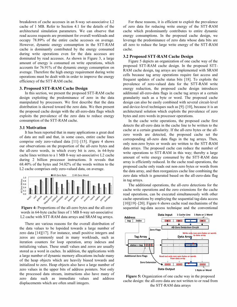
3.2 Proposed STT-RAM Cache Design Figure 5 depicts an organization of one cache way of the
proposed STT-RAM cache design. In the proposed STT-
RAM cache design, tag arrays are implemented with SRAM
cells because tag array operations require fast access and
frequent updates of cache status bits [18]. To exploits the
prevalence of zero-valued data for the STT-RAM write
energy reduction, the proposed cache design introduces
additional all-zero-data flags in cache tag arrays at a certain
granularity such as a byte or word. The proposed cache
design can also be easily combined with several circuit-level
and device-level techniques such as [9]–[10], because it is an
architectural solution which exploits the prevalence of zero
bytes and zero words in processor operations.
In the cache write operations, the proposed cache first
detects the all-zero data in the cache line to be written to the
cache at a certain granularity. If the all-zero bytes or the all-
zero words are detected, the proposed cache set the
corresponding all-zero data flags in the tag arrays. Then,
only non-zero bytes or words are written to the STT-RAM
data arrays. The proposed cache can reduce the number of
write operations to STT-RAM in this way; thereby a large
amount of write energy consumed by the STT-RAM data
array is efficiently reduced. In the cache read operations, the
proposed cache only reads out non-zero bytes or words from
the data array, and then reorganizes cache line combining the
zero data which is generated based on the all-zero-data flag
in tag arrays.
The additional operations, the all-zero detections for the
cache write operations and the zero extensions for the cache
read operations, can be executed simultaneously with other
cache operations by employing the sequential tag-data access
[10][19]–[20]. Figure 6 shows cache read mechanisms of the
sequential tag-data access technique and the conventional
indextag
Tag Array
1 1 0 1
Additional Zero Flags
status + tag
Address0000 0000 0000
Data Input
Write only non-zero bytes or wordsto data array
Data Array
1 Byte or 1 Word1 Cache Line
All-Zero Detection Circuit
Data Output
0000 0000 0000
1 Byte or Word
Zero Extension
Zero Flags
Read out only non-zero bytes or wordsfrom data array
Figure 5: Organization of one cache way in the proposed
cache design: the all-zero data are not written to or read from
the STT-RAM data arrays
Page 4
cache access mechanism. Note that cache write operations
for both the schemes are inherently conducted tag-data
sequentially. In the sequential tag-data access, the cache first
retrieves its tag arrays and accesses the data array at which a
cache hit occurs. Actually, sequential tag-data access is
usually leveraged in large, lower-level caches of modern
microprocessors due to its energy efficiency [19][20].
Therefore, in this paper, we choose the sequential tag-data
access as a baseline cache access mechanism.
In the proposed cache design, the all-zero data detection
in write operations is executed retrieving the tag in tag arrays.
Also, the zero extension for read operations is executed
simultaneously with the data array access based on the all-
zero-data flags which are read out from the tag array in tag
access phase. Therefore we can hide the cycle penalty of the
additional zero detections and extensions in the proposed
cache design.
The proposed cache design may seem to be similar to the
cache energy reduction techniques such as the partial write
or selective cache write scheme [10][21] in the way that they
exploit the characteristics of the processed data. These
techniques leverage the observation that many of data
written to the cache has the same values which are already
stored in the cache. Therefore they need a dummy read
operation to check whether the data to be written to the
cache is changed from the resident data. On the other hand,
the proposed cache exploits the predominance of the zero in
the data which are manipulated by processors. Note that it is
possible to detect zero data in our scheme using only the
data which is written to the cache without comparing to
resident data. Therefore, in contrast with these techniques,
the proposed cache does not need dummy reads which give
rise to performance degradations. The proposed cache
design could give us another chance to reduce the energy
consumption of on-chip caches.
4. Experimental Results In the following subsections, we describe experimental
results of the proposed STT-RAM cache design. We conduct
experiments under the assumption that the proposed cache is
used for L2 cache of 1 MB which comprises SRAM tag
arrays and STT-RAM data arrays. To begin with, we
describe our experimental methodology for evaluating the
proposed cache design. We then present the estimation of
the timing- and energy-related parameters of the proposed
cache. We also analyze the impact of the proposed cache
design on processor performance. Following the evaluation
results of performance, energy consumption of the proposed
cache is evaluated in terms of both the dynamic energy and
the total energy consumption.
4.1. Methodology Table 4 describes the baseline processor parameters used
in our experimental evaluations. We used the gem5
architectural simulator [22] for the evaluation of the
proposed cache design, which was modified to simulate the
all-zero-data flags. We chose a processor with 2-way set-
associative L1 instruction and 8-way set-associative L1 data
caches of 32 KB each and a unified 8-way set-associative L2
cache of 1 MB as the baseline. We assumed that the L1
cache is implemented with SRAM, because it requires fast
operations, and therefore has the identical latencies for both
read and write operations. The details of the read and write
latencies of the L2 cache in Table 4 are given below in
Section 4.2. We chose eight benchmarks from SPEC2006
CINT and seven benchmarks from SPEC2006 CFP
benchmarks [23]. All the simulations were executed for two
billion instructions with warm-up period for one billion
instructions.
Table 4: Baseline processor configuration
Parameter Value
Processor frequency 3 GHz
L1 instruction cache 32-KB, 2-way, 64-byte cache line,
2-cycle access time
L1 data cache 32-KB, 8-way, 64-byte cache line,
2-cycle access time
Unified L2 cache
1 MB, 8-way, 64-byte cache line,
8-cycle read latency,
35-cycle write latency
Cache replacement policy Least recently used (LRU)
To evaluate the proposed cache design, we used our
modified version of CACTI 6.5 [24] for modeling the
general cache peripherals and SRAM tag arrays. We
modeled timing- and energy-related cache parameters, such
as read and write latencies, dynamic energy consumption per
cache access, area, and leakage. As described above, we
chose a 1-MB 8-way set-associative L2 cache with STT-
RAM data arrays and SRAM tag arrays as a baseline cache
design which is implemented in 45 nm process technology.
We selected the byte and word granularities for the
granularity of the additional all-zero-data flags. The
additional circuits for the proposed cache were synthesized
and implemented in a 45-nm CMOS technology with
Synopsys Design Compiler®. For the STT-RAM technology-
related cell parameters, we referred to the several previous
works [7]–[9] and scaled them to 45-nm process.
4.2. Modeling of Proposed STT-RAM Cache Table 1 lists the estimated read and write latencies of
STT-RAM data array and SRAM tag array in the proposed
(2) Data Access (If Cache Hit)Tag Array Data Array
Hit way
(1) Tag Accesses
Tag Array Data Array
Sequential Tag-Data Access Conventional Cache Access
(1) Parallel Tag and Data Accesses
Data Array
(2) Data Selection (If Cache Hit)Tag Array Data Array
Hit way
Tag Array
Figure 6: Comparison of cache read mechanisms
between the sequential tag-data access and the conventional
parallel tag-data access mechanisms.
Page 5
designs. We set STT-RAM write pulse width to 10 ns as
stated above in Section 2. In the proposed cache, the access
latency of the SRAM tag array with the all-zero-data flags at
the byte granularity (the all-zero-byte flags: AZBF) is larger
than that of the tag array with the all-zero-data flags at the
word granularity (the all-zero-word flags: AZWF): They are
signified as AZBF and AZWF in Table 1 and hereafter in
this paper. It is because, for the cache lines of 64 bytes, the
proposed cache design with AZBF appends additional 64
bits in the SRAM tag array in each cache way whereas the
proposed cache with AZWF adds 16 bits in the tag arrays.
The large latencies of the tag arrays in the proposed design
result from increased access time of SRAM arrays. Note that
the STT-RAM data arrays in both of the implementations are
identical to the baseline.
Table 1: Read and write latencies in the proposed cache
Attribute STT-RAM
data Array
Tag array
(Baseline)
Tag array
(w/ AZBF)
Tag array
(w/ AZWF)
Read Latency 1.507 ns 0.743 ns 0.831 ns 0.762 ns
Write Latency 10.571 ns 0.743 ns 0.831 ns 0.762 ns
Table 2 shows the dynamic energy per read and write
accesses consumed by each element. The STT-RAM data
arrays are accessed on the byte granularity for the proposed
cache with AZBF and on the word granularity with AZWF.
Therefore we estimated the dynamic energy per access to the
data array consumed by the STT-RAM cells in Table 2 at
both the granularities. The dynamic energy consumption per
cache operation of the baseline design in Table 2 is the
energy consumed on one cache line access. The second row
in Table 2 denotes the dynamic energies consumed by all tag
arrays in the cache and additional peripheral circuitries. Note
that every tag array is retrieved in each cache access. The
proposed cache design with AZBF has larger per-access
dynamic energy for tag accesses and peripherals mainly due
to its large amounts of additional bits in tag arrays.
Table 2: Dynamic energy per cache access
Baseline w/ AZBF w/AZWF
Read
(1 line) Write
(1 line) Read
(1 byte) Write
(1 byte) Read
(1 word) Write
(1word)
STT-RAM
Cells 0.013 nJ 1.417 nJ 0.203 pJ 22.13 pJ 0.813 pJ 88.53 pJ
Tag accesses
peripherals 0.114 nJ 0.095 nJ 0.145 nJ 0.125 nJ 0.122 nJ 0.103 nJ
Based on estimated dynamic energies consumed by each
element in Table 2, the dynamic energy per cache access of
the proposed design can be calculated as:
cellszero-nontagsdynamic ×+= ENEE (1)
where Etags, Nnon-zero and Ecells are the energy consumed by
tag accesses and peripherals, the number of non-zero data in
a cache line to be read from or written to the cache, and the
energy consumed by the STT-RAM cells in data arrays,
respectively. The value of Nnon-zero varies depending on the
data to be read from or written to the cache. Its maximum
value is bounded by the size of cache line; for the 64-byte
cache line, the proposed cache design has 64 of the
maximum value of Nnon-zero at the byte granularity, and 16 at
the word granularity.
We also estimated area and leakage of the proposed
cache design as shown in Table 3. Due to its larger SRAM
tag arrays, the proposed cache with AZBF shows higher
leakage and area, which are increased by 50.13% and
20.97%, respectively, in comparison with the baseline cache
design. The proposed cache with AZWF, on the other hand,
shows relatively small overhead in leakage and area which
are 13.37% and 5.81%, respectively.
Table 3: Estimated leakage and area.
Attribute Baseline w/ AZBF w/ AZWF
Leakage (mW) 4.4955 6.7494 5.0966
Normalized leakage 1 1.5013 1.1337
Area (mm2) 2.3131 2.7982 2.4301
Normalized area 1 1.2097 1.0581
4.3. Performance As discussed in Section 3, the proposed cache design
introduces no cycle penalties to write operations because the
all-zero data detection for the proposed cache design can be
simultaneously operated with tag array accesses. It is also
pointed out that no cycle penalties are introduced on read
operations as the zero extension is executed during the data
array access phase. Therefore, there is no need to consider
the processor performance overhead caused by the additional
operations of the proposed cache. Processor performance is
rather improved by adopting the proposed cache, if cache
lines that are written to or read out from the cache are
comprised of only all-zero bytes or all-zero words. In other
words, every bit in a cache line consists of only zero. This is
because data array accesses can be cut out in that situation.
0.00.20.40.60.81.01.21.4
No
rmal
ized
IPC
Baseline w/ AZBF w/ AZWF
Figure 7: Normalized IPC evaluation results.
Figure 7 shows the normalized instructions per cycles
(IPCs) of each workload in the SPEC2006 benchmark suite.
We observe that the proposed cache design improves
processor IPC by 5.44% on average. Moreover, not only are
there no performance losses, but the proposed cache design
largely improves IPC over 10% for the workloads such as
“libquantum”, “bwaves” and “zeusmp”; These benchmarks
are memory intensive and contain huge amount of all-zero-
data as shown in Figure 4. Note that the proposed cache
designs at both the granularities are equivalent in terms of
Page 6
processor performance because the numbers of cache lines
comprising only zero bits, which a processor manipulates,
are invariable in identical conditions.
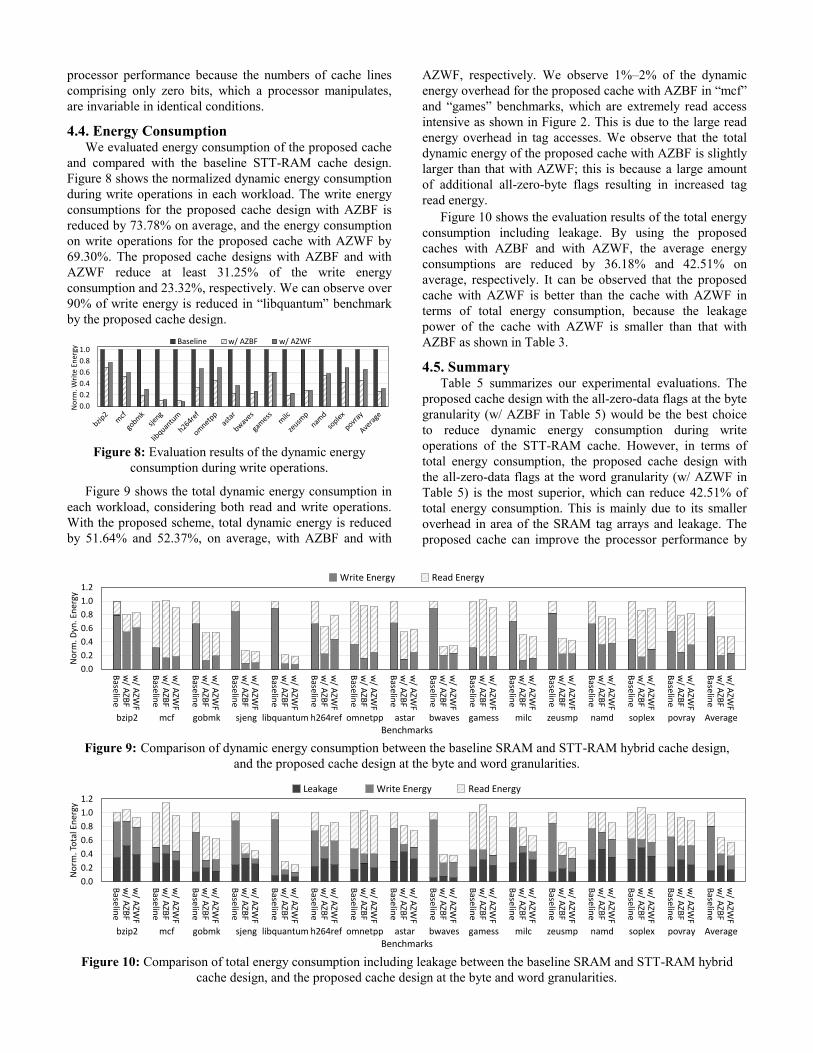
4.4. Energy Consumption We evaluated energy consumption of the proposed cache
and compared with the baseline STT-RAM cache design.
Figure 8 shows the normalized dynamic energy consumption
during write operations in each workload. The write energy
consumptions for the proposed cache design with AZBF is
reduced by 73.78% on average, and the energy consumption
on write operations for the proposed cache with AZWF by
69.30%. The proposed cache designs with AZBF and with
AZWF reduce at least 31.25% of the write energy
consumption and 23.32%, respectively. We can observe over
90% of write energy is reduced in “libquantum” benchmark
by the proposed cache design.
0.0
0.2
0.4
0.6
0.8
1.0
No
rm. W
rite
En
ergy
Baseline w/ AZBF w/ AZWF
Figure 8: Evaluation results of the dynamic energy
consumption during write operations.
Figure 9 shows the total dynamic energy consumption in
each workload, considering both read and write operations.
With the proposed scheme, total dynamic energy is reduced
by 51.64% and 52.37%, on average, with AZBF and with
AZWF, respectively. We observe 1%–2% of the dynamic
energy overhead for the proposed cache with AZBF in “mcf”
and “games” benchmarks, which are extremely read access
intensive as shown in Figure 2. This is due to the large read
energy overhead in tag accesses. We observe that the total
dynamic energy of the proposed cache with AZBF is slightly
larger than that with AZWF; this is because a large amount
of additional all-zero-byte flags resulting in increased tag
read energy.
Figure 10 shows the evaluation results of the total energy
consumption including leakage. By using the proposed
caches with AZBF and with AZWF, the average energy
consumptions are reduced by 36.18% and 42.51% on
average, respectively. It can be observed that the proposed
cache with AZWF is better than the cache with AZWF in
terms of total energy consumption, because the leakage
power of the cache with AZWF is smaller than that with
AZBF as shown in Table 3.
4.5. Summary Table 5 summarizes our experimental evaluations. The
proposed cache design with the all-zero-data flags at the byte
granularity (w/ AZBF in Table 5) would be the best choice
to reduce dynamic energy consumption during write
operations of the STT-RAM cache. However, in terms of
total energy consumption, the proposed cache design with
the all-zero-data flags at the word granularity (w/ AZWF in
Table 5) is the most superior, which can reduce 42.51% of
total energy consumption. This is mainly due to its smaller
overhead in area of the SRAM tag arrays and leakage. The
proposed cache can improve the processor performance by
bzip2 mcf Averagegobmk sjeng libquantum h264ref omnetpp astar bwaves gamess milc zeusmp namd soplex povray
0.0
0.2
0.4
0.6
0.8
1.0
1.2
Baselin
ew
/ AZB
Fw
/ AZW
F
Baselin
ew
/ AZB
Fw
/ AZW
F
Baselin
ew
/ AZB
Fw
/ AZW
F
Baselin
ew
/ AZB
Fw
/ AZW
F
Baselin
ew
/ AZB
Fw
/ AZW
F
Baselin
ew
/ AZB
Fw
/ AZW
F
Baselin
ew
/ AZB
Fw
/ AZW
F
Baselin
ew
/ AZB
Fw
/ AZW
F
Baselin
ew
/ AZB
Fw
/ AZW
F
Baselin
ew
/ AZB
Fw
/ AZW
F
Baselin
ew
/ AZB
Fw
/ AZW
F
Baselin
ew
/ AZB
Fw
/ AZW
F
Baselin
ew
/ AZB
Fw
/ AZW
F
Baselin
ew
/ AZB
Fw
/ AZW
F
Baselin
ew
/ AZB
Fw
/ AZW
F
Baselin
ew
/ AZB
Fw
/ AZW
FN
orm
. Dyn
. En
ergy
Write Energy Read Energy
Benchmarks Figure 9: Comparison of dynamic energy consumption between the baseline SRAM and STT-RAM hybrid cache design,
and the proposed cache design at the byte and word granularities.
bzip2 mcf Averagegobmk sjeng libquantum h264ref omnetpp astar bwaves gamess milc zeusmp namd soplex povray
0.0
0.2
0.4
0.6
0.8
1.0
1.2
Base
line
w/ A
ZBF
w/ A
ZWF
Base
line
w/ A
ZBF
w/ A
ZWF
Base
line
w/ A
ZBF
w/ A
ZWF
Base
line
w/ A
ZBF
w/ A
ZWF
Base
line
w/ A
ZBF
w/ A
ZWF
Base
line
w/ A
ZBF
w/ A
ZWF
Base
line
w/ A
ZBF
w/ A
ZWF
Base
line
w/ A
ZBF
w/ A
ZWF
Base
line
w/ A
ZBF
w/ A
ZWF
Base
line
w/ A
ZBF
w/ A
ZWF
Base
line
w/ A
ZBF
w/ A
ZWF
Base
line
w/ A
ZBF
w/ A
ZWF
Base
line
w/ A
ZBF
w/ A
ZWF
Base
line
w/ A
ZBF
w/ A
ZWF
Base
line
w/ A
ZBF
w/ A
ZWF
Base
line
w/ A
ZBF
w/ A
ZWF
No
rm. T
ota
l En
erg
y
Leakage Write Energy Read Energy
Benchmarks Figure 10: Comparison of total energy consumption including leakage between the baseline SRAM and STT-RAM hybrid
cache design, and the proposed cache design at the byte and word granularities.
Page 7
5.45% at both the granularities of additional zero flags.
5. Conclusion In this paper, we proposed an STT-RAM cache design
technique which can efficiently reduce dynamic energy
consumption of STT-RAM during write operations and
thereby total energy consumption. The proposed cache
design exploits the observation that there are a large number
of zero-valued data in many applications. The proposed
cache design appends the all-zero-data flags at a certain
granularity in cache tag arrays and set these flags if the
corresponding data in the cache line to be written to the
cache is zero-valued data. Experimental results show that the
proposed cache can reduce 73.78% and 69.30% of the
dynamic energy on write operations with the all-zero-data
flags at the byte and word granularities, respectively. This
results in 36.18% less total energy consumption using the
proposed cache with the byte granularity flags and 42.51%
with the word granularity. Performance evaluation results
also show that the proposed cache design can improve
processor performance by 5.44% on average. Our proposed
cache design provides an efficient solution to reduce the
energy consumption of the STT-RAM cache.
Acknow ledgment This work was supported by The Ministry of Economy,
Trade and Industry (METI), and The New Energy and
Industrial Technology Development Organization (NEDO).
References [1] S. Kaxiras and M. Martonosi, “Cache decay: exploiting generational
behavior to reduce cache leakage power,” in Proceedings of the 28th Annual International Symposium on Computer Architecture, pp. 240–251, May 2001.
[2] B. Rogers, A. Krishna, G.Bell, K. Vu, X. Jiang, and Y. Solihin, “Scaling the Bandwidth Wall: Challenges in and Avenues for CMP Scaling,” in Proceedings of the 36th Annual International Symposium on Computer Architecture, pp. 371–382, Jun. 2009.
[3] N. Kim, T. Austin, D. Blaauw, T. Mudge, K. Flautner, M. Irwin, M. Kandemir, and V. Narayanan, “Leakage current: Moore’s law meets static power,” in IEEE Computer, vol. 36, no. 12, pp. 68–75, Dec. 2003.
[4] N. Kim, K. Flautner, D. Blaauw, and T. Mudge, “Drowsy Instruction Caches: Leakage Power Reduction using Dynamic Voltage Scaling and Cache Sub-bank Prediction,” in Proceedings of the 35th Annual ACM/IEEE International Symposium on Microarchitecture, pp. 219–230, Nov. 2002.
[5] K. Roy, S. Mukhopadhyay, and H. Mahmoodi-Meimand, “Leakage Current Mechanisms and Leakage Reduction Techniques in Deep-
submicrometer CMOS Circuits,” in Proceedings of the IEEE, vol. 91, no. 2, pp. 305–327, Feb. 2003.
[6] ITRS Report 2011, Available: http://www.itrs.net/.
[7] X. Dong, X. Wu, G. Sun, Y. Xie, H. Li, and Y. Chen, “Circuit and Microarchitecture Evaluation of 3D Stacking Magnetic RAM (MRAM) as a Universal Memory Replacement,” in Proceedings of the 45th Annual Design Automation Conference, pp. 554–559, Jun. 2008.
[8] G. Sun, X. Dong, Y. Xie, J. Li, and Y. Chen, “A Novel Architecture of the 3D Stacked MRAM L2 Cache for CMPs,” in Proceedings of IEEE 15th International Symposium on High Performance Computer Architecture, pp. 239–249, Feb. 2009.
[9] P. Zhou, B. Zhao, J. Yang, and Y. Zhang, “Energy Reduction for STT-RAM Using Early Write Termination,” in Proceedings of the 2009 International Conference on Computer-Aided Design, pp. 264–268, Nov. 2009.
[10] S. Park, S. Gupta, N. Mojumder, A. Raghunathan, and K. Roy, “Future Cache Design using STT MRAMs for Improved Energy Efficiency,” in Proceedings of the 49th Annual Design Automation Conference, pp. 492–497. Mar. 2012.
[11] M. Ekman and P. Stenstrom, “A Robust Main-memory Compression Scheme,” in Proceedings of the 32nd Annual International Symposium on Computer Architecture, pp. 74–85, Jun. 2005.
[12] L. Villa, M. Zhang, and K. Asanović, “Dynamic Zero Compression for Cache Energy Reduction,” in Proceedings of the 33rd Snnual ACM/IEEE International Symposium on Microarchitecture, pp. 214–220, Dec. 2000.
[13] J. Dusser, T. Piquet, and A. Seznec, “Zero-Content Augmented Caches,” in Proceedings of the 23rd International Conference on Conference on Supercomputing, pp. 46–55, Jun. 2009.
[14] Y. Chang and F. Lai, “Dynamic Zero-Sensitivity Scheme for Low-Power Cache Memories,” in IEEE Micro, vol. 25, no. 4, pp. 20–32, Jul. 2005.
[15] A. Moshovos, B. Falsafi, F. Najm, and N. Azizi, “A Case for Asymmetric-Cell Cache Memories,” in IEEE Transactions on Very Large Scale Integration (VLSI) Systems, vol. 13, no. 7, pp. 877–881, Jul. 2005.
[16] J. Zhu, “Magnetoresistive Random Access Memory: The Path to Competitiveness and Scalability,” in Proceedings of the IEEE, vol. 96, no. 11, pp. 1786–1798, Nov. 2008.
[17] M. Hosomi et al., “A Novel Nonvolatile Memory with Spin Torque Transfer Magnetization Switching: Spin-RAM,” in Proceedings of IEEE International Electron Devices Meeting, pp. 459–462, Dec. 2005.
[18] M. Rasquinha, D. Choudhary, S. Chatterjee, S. Mukhopadhyay, and S. Yalamanchili, “An Energy Efficient Cache Design Using Spin Torque Transfer (STT) RAM,” in Proceedings of the 16th ACM/IEEE International Symposium on Low Power Electronics and Design, pp. 389–394, Aug. 2010.
[19] Z. Chishti, M. Powell, and T. Vijaykumar, “Distance Associativity for High-Performance Energy-Efficient Non-Uniform Cache Architectures,” in Proceedings of the 36th Annual ACM/IEEE International Symposium on Microarchitecture, pp. 55–66, Dec. 2003.
[20] D. Weiss, J. Wuu, and V. Chin, “The On-Chip 3-MB Subarray-Based Third-Level Cache on an Itanium Microprocessor,” in IEEE Journal of Solid-State Circuits, vol. 37, no. 11, pp. 1523–1529, Nov. 2002.
[21] W. Xu, J. Liu, and T. Zhang, “Data Manipulation Techniques to Reduce Phase Change Memory Write Energy,” in Proceedings of the 14th ACM/IEEE International Symposium on Low Power Electronics and Design, pp. 237–242, Aug. 2009.
[22] N. Binkert et al., “The gem5 Simulator,” in ACM SIGARCH Computer Architecture News, vol. 39, no. 2, pp. 1–7, Aug. 2011.
[23] Standard Performance Evaluation Corporation, “The SPEC CPU 2006 Benchmark Suite,” Available: http://www.specbench.org.
[24] N. Muralimanohar, R. Balasubramonian, and N. Jouppi, ”CACTI 6.0: A Tool to Model Large Caches,” Technical Report HPL-2009-85, Hewlett Packard Laboratories, 2009
Table 5: Summary of experimental evaluations
Attribute Baseline w/ AZBF w/ AZWF
Area (mm2) 2.3131 2.7982 2.4301
Leakage (mW) 4.4955 6.7494 5.0966
Processor IPC
(normalized) 1 1.0544 1.0544
Write energy
(normalized) 1 0.2622 0.3070
Dynamic energy
(normalized) 1 0.4836 0.4763
Total energy
(normalized) 1 0.6382 0.5749