9 Energy-Efficient Encoding Techniques for Off-Chip Data Buses DINESH C. SURESH, BANIT AGRAWAL, JUN YANG, and WALID NAJJAR University of California, Riverside Reducing the power consumption of computing devices has gained a lot of attention recently. Many research works have focused on reducing power consumption in the off-chip buses as they consume a significant amount of total power. Since the bus power consumption is proportional to the switching activity, reducing the bus switching is an effective way to reduce bus power. While numerous techniques exist for reducing bus power in address buses, only a handful of techniques have been proposed for data-bus power reduction, where frequent value encoding (FVE) is the best existing scheme to reduce the transition activity on the data buses. In this article, we propose improved frequent value data bus-encoding techniques aimed at reducing more switching activity and, hence, power consumption. We propose three new schemes and five new variations to exploit bit-wise temporal and spatial locality in the data-bus values. Our techniques just use one external control signal and capture bit-wise locality to efficiently encode data values. For all the embedded and SPEC applications we tested, the overall average switching reduction is 53% over unencoded data and 10% more than the conventional FVE scheme. Categories and Subject Descriptors: B.7.1 [Integrated Circuits]: Types and Design Styles—In- put/output circuits; B.4.m [Input/output and Data Communications]: Miscellaneous General Terms: Design, Performance, Measurement. Additional Key Words and Phrases: Low-power data buses, encoding, bus switching, internal capacitances ACM Reference Format: Suresh, D. C., Agrawal, B., Yang, J., and Najjar W. 2009. Energy-efficient encoding techniques for off-chip data buses. ACM Trans. Embedd. Comput. Syst. 8, 2, Article 9 (January 2009), 23 pages. DOI = 10.1145/1457255.1457256 http://doi.acm.org/10.1145/1457255.1457256 1. INTRODUCTION Power dissipation is a critical design criterion for embedded systems and espe- cially for mobile computing devices [Semiconductor Industry Association 2003]. These devices often draw their current from batteries that place a limited amount of energy at the system’s disposal. Consequently, reduced power and Authors’ addresses: D. C. Suresh, B. Agrawal, J. Yang, and W. Najjar, Department of Computer Science and Engineering, University of California, Riverside; email: [email protected]. Permission to make digital or hard copies of part or all of this work for personal or classroom use is granted without fee provided that copies are not made or distributed for profit or direct commercial advantage and that copies show this notice on the first page or initial screen of a display along with the full citation. Copyrights for components of this work owned by others than ACM must be honored. Abstracting with credit is permitted. To copy otherwise, to republish, to post on servers, to redistribute to lists, or to use any component of this work in other works requires prior specific permission and/or a fee. Permissions may be requested from Publications Dept., ACM, Inc., 2 Penn Plaza, Suite 701, New York, NY 10121-0701 USA, fax +1 (212) 869-0481, or [email protected]. C 2009 ACM 1539-9087/2009/01-ART9 $5.00 DOI 10.1145/1457255.1457256 http://doi.acm.org/ 10.1145/1457255.1457256 ACM Transactions on Embedded Computing Systems, Vol. 8, No. 2, Article 9, Publication date: January 2009.
Transcript
9
Energy-Efficient Encoding Techniquesfor Off-Chip Data Buses
DINESH C. SURESH, BANIT AGRAWAL, JUN YANG, and WALID NAJJAR
University of California, Riverside
Reducing the power consumption of computing devices has gained a lot of attention recently. Many
research works have focused on reducing power consumption in the off-chip buses as they consume a
significant amount of total power. Since the bus power consumption is proportional to the switching
activity, reducing the bus switching is an effective way to reduce bus power. While numerous
techniques exist for reducing bus power in address buses, only a handful of techniques have been
proposed for data-bus power reduction, where frequent value encoding (FVE) is the best existing
scheme to reduce the transition activity on the data buses.
In this article, we propose improved frequent value data bus-encoding techniques aimed at
reducing more switching activity and, hence, power consumption. We propose three new schemes
and five new variations to exploit bit-wise temporal and spatial locality in the data-bus values. Our
techniques just use one external control signal and capture bit-wise locality to efficiently encode
data values. For all the embedded and SPEC applications we tested, the overall average switching
reduction is 53% over unencoded data and 10% more than the conventional FVE scheme.
Categories and Subject Descriptors: B.7.1 [Integrated Circuits]: Types and Design Styles—In-put/output circuits; B.4.m [Input/output and Data Communications]: Miscellaneous
General Terms: Design, Performance, Measurement.
Additional Key Words and Phrases: Low-power data buses, encoding, bus switching, internal
capacitances
ACM Reference Format:Suresh, D. C., Agrawal, B., Yang, J., and Najjar W. 2009. Energy-efficient encoding techniques for
DOI = 10.1145/1457255.1457256 http://doi.acm.org/10.1145/1457255.1457256
1. INTRODUCTION
Power dissipation is a critical design criterion for embedded systems and espe-cially for mobile computing devices [Semiconductor Industry Association 2003].These devices often draw their current from batteries that place a limitedamount of energy at the system’s disposal. Consequently, reduced power and
Authors’ addresses: D. C. Suresh, B. Agrawal, J. Yang, and W. Najjar, Department of Computer
Science and Engineering, University of California, Riverside; email: [email protected].
Permission to make digital or hard copies of part or all of this work for personal or classroom use is
granted without fee provided that copies are not made or distributed for profit or direct commercial
advantage and that copies show this notice on the first page or initial screen of a display along
with the full citation. Copyrights for components of this work owned by others than ACM must be
honored. Abstracting with credit is permitted. To copy otherwise, to republish, to post on servers,
to redistribute to lists, or to use any component of this work in other works requires prior specific
permission and/or a fee. Permissions may be requested from Publications Dept., ACM, Inc., 2 Penn
ACM Transactions on Embedded Computing Systems, Vol. 8, No. 2, Article 9, Publication date: January 2009.
9:2 • D. C. Suresh et al.
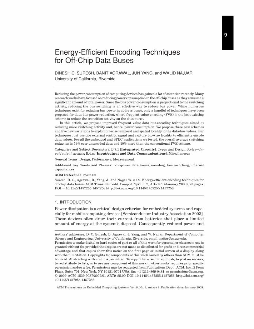
Fig. 1. Average normalized hits for FV, MSB and LSB.
energy consumption of embedded devices translates to longer battery lives andreduced cooling requirements.
Off-chip and On-chip bus lines in VLSI circuits are associated with verylarge capacitances and they are a major contributor to a system’s total powerconsumption. The power consumption in the bus drivers is in direct proportionto the product of the average number of signal transitions and the line ca-pacitance. Capacitive load of off-chip buses is orders of magnitude larger thanthat of internal switching nodes [Chern et al. 1992; Givargis and Vahid 1998;Weste and Eshraghian 1998]. At the expense of a small internal energy costbus-encoding schemes encode bus values to significantly reduce the bus powerduring off-chip-transmission.
Both address and data streams are amenable to encoding. Efficient schemesto exploit the sequential and stride behavior of instruction address streamshave been proposed [Basu et al. 2002; Benini et al. 2000; Givargis and Vahid1998; Stan and Burleson 1995]. However, the difficulty in encoding off-chip databus values lies in the fact that off-chip data streams are less regular.
In off-chip data traces, the high order bits (MSBs) and the low order bits(LSBs) of a data value occur a lot more frequently than the entire data value.For example, if the value 80485678 occurs 10,000 times, then one could safelyassume that 8048 occurs at least 10,000 times in the high-order bits, and thevalue 5678 occurs at least 10,000 times in the low-order bits of data values. Inother words, partial data value locality is at least as abundant as data valuelocality. We propose that, besides storing the values encountered in the recentpast, the high- and low-order bits of the values should also be stored in separatetables. The intuition behind doing so is that, for every repeating data value,there might be many nonrepeating data values that contain the same high-or low-order bits. Throughout this article, we will refer to repeating values asfrequent values (FV) and nonrepeating values as nonfrequent values.
Figure 1 shows the average normalized hits for the MSB, LSB, and the MSB-LSB portions of data values for the benchmarks in NetBench, MediaBench, andthe SPEC2000 application suites. A scheme that encodes both the MSB and LSBportions besides encoding the entire data values can efficiently exploit the largehit rate in the MSB and LSB portions. Throughout this article, we will refer tothis scheme as the FV-MSB-LSB scheme.
ACM Transactions on Embedded Computing Systems, Vol. 8, No. 2, Article 9, Publication date: January 2009.
Energy-Efficient Encoding Techniques for Off-Chip Data Buses • 9:3
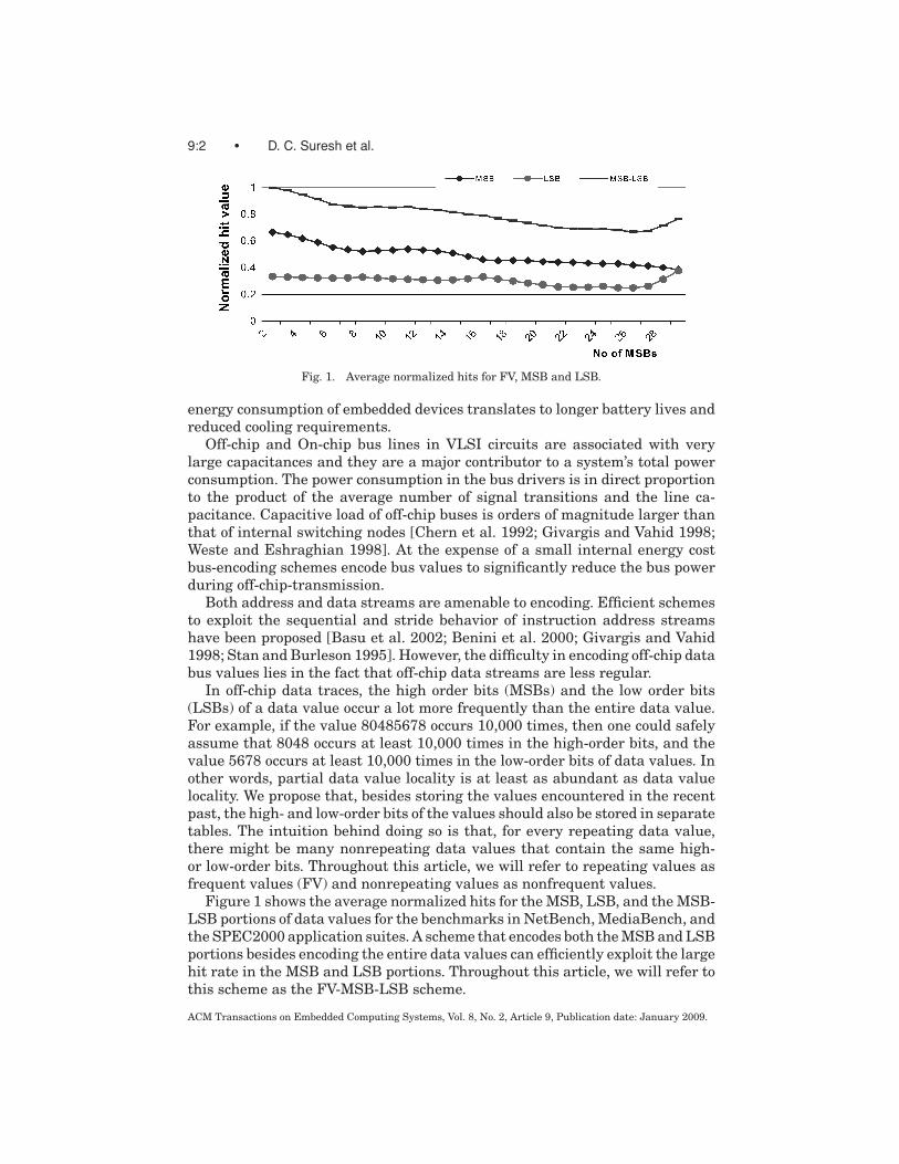
Fig. 2. Common strides of repeating values in Jpegdecode benchmark.
To better understand the need for caching the entire as well as partial datavalues we evaluated the following: for each repeating data value, we measuredthe number of cycles it takes for the value or its portion to recur. Figure 2 sum-marizes our results for the Jpegdecode benchmark [Burger and Austin 1997].The x-axis shows the bit-width of the values under consideration and the y-axisshows the percentage contribution of values occurring within k-cycles (k = 1,15, 60, and >60). For entire data values (32-bits wide), 30% of the frequent val-ues repeat within the next cycle. When a value repeats in consecutive cycles, itdoes not result in any off-chip bus transitions even in the absence of an encodingscheme. Hence, encoding such occurrences of frequent values would not yieldany significant energy savings. Nearly 33% of the hits shown in Figure 2 repeatwithin a span of 15 cycles. Encoding such values would yield higher savings.About 20% of the repeating data values recur after 60 cycles. Data values ofsmaller widths repeat more frequently than data values of larger width. Hence,encoding schemes that can capitalize on temporal locality in both entire and par-tial data values would be highly effective in reducing the energy consumption.
In this article, we propose three novel data bus-encoding schemes to reducepower consumption in the off-chip data buses. FV-i encoding extends the fre-quent value encoding (FVE) [Yang and Gupta 2001] scheme to maintain a largerwindow of recently encountered data values and is, hence, capable of encodingmore data values than the original FVE scheme. FV-i-MSB-j encodes both entiredata values and the most significant bits (MSB) portions of repeating data val-ues. FV-MSB-LSB encodes entire data values as well as the MSB/LSB portionsof data values. The FV-MSB-LSB scheme provides an average energy reduc-tion of 53% over unencoded data and yields an additional 10% improvement inenergy on top of FVE.
The remainder of this article is organized as follows. In Section 2, we discussthe related work. In Section 3, we describe our data bus-encoding schemesand its variations. In Section 4, we describe our experimental framework. InSection 5, we evaluate the energy consumption of our schemes and the energyconsumed in the off-chip bus. In Section 6, we analyze the impact of our encodingschemes on performance of the system, and in Section 7, we conclude.
ACM Transactions on Embedded Computing Systems, Vol. 8, No. 2, Article 9, Publication date: January 2009.
9:4 • D. C. Suresh et al.
2. RELATED WORK
Data bus-encoding schemes, like bus-invert coding [Stan and Burleson 1995]adaptive coding [Komatsu et al. 1999], and FVE [Yang et al. 2004; Zhang et al.2000], do not assume any prior knowledge of the application. A scheme thatoperates without prior knowledge of input data is highly desirable because inmany application-domains, knowing the data in advance might prove to be avery stringent requirement.
Bus-invert coding [Stan and Burleson 1995] transfers a data value eitherin its original form or in its complement form depending on whose hammingdistance with the previous bus transmission is smaller. An external complementsignal is used to let the destination know that the value sent on the bus is inone’s complement form, and hence, it should not be interpreted as is. It is asimple method that assumes values are uniformly distributed across the entirevalue space.
The adaptive encoding scheme [Benini et al. 1997], taking the next step fur-ther, is capable of online adaptation to the value streams by learning the statis-tics on the fly. As collecting the accurate statistics for the value streams can bevery expensive, the proposed adaptive encoding operates bit-wise rather thanword-wise. Thus, it loses the correlation among the bits within a single value.
Gray code encoding [Su et al. 1994] capitalizes on the observation that con-secutive values are often sent during successive bus cycles. If gray code wasused for representing addresses, sending consecutive values would result inonly one transition on the bus. In T0 encoding 3, an external control signal isused to indicate that the current and previous bus values differ by one, andthere is no transition activity in the bus wires while sending the second value.Though these schemes work well with address streams, they do not work wellwith data streams because sequential data values are rarely sent on successivebus cycles.
Bus expander [Citron and Rudolph 1995] and dynamic base register caching(DBRC) [Ferrens and Park 1991] propose compaction techniques to increase theeffective bus-width. DBRC uses dynamically allocated base registers to cachethe higher order bits of address values. Ramprasad et al. [1999] applied a gen-eral communication model to analyze the bus-encoding schemes. Victor andKeutzer [2001] address the problem of minimizing effect of interwire capac-itance by converting a data value sequence into a self-shielding sequence inwhich no two adjacent bus lines change in opposite directions at the same time.For a 32-bit bus, this scheme needs additional 14 bus lines in order to minimizethe cross-talk delay.
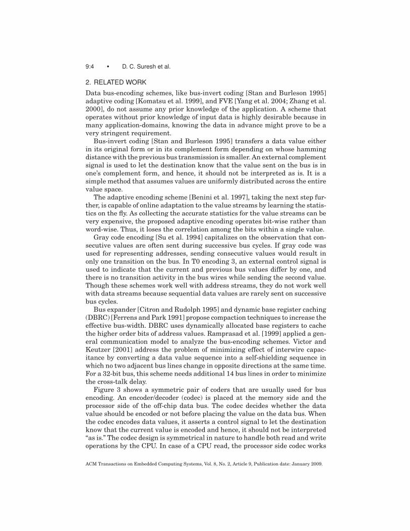
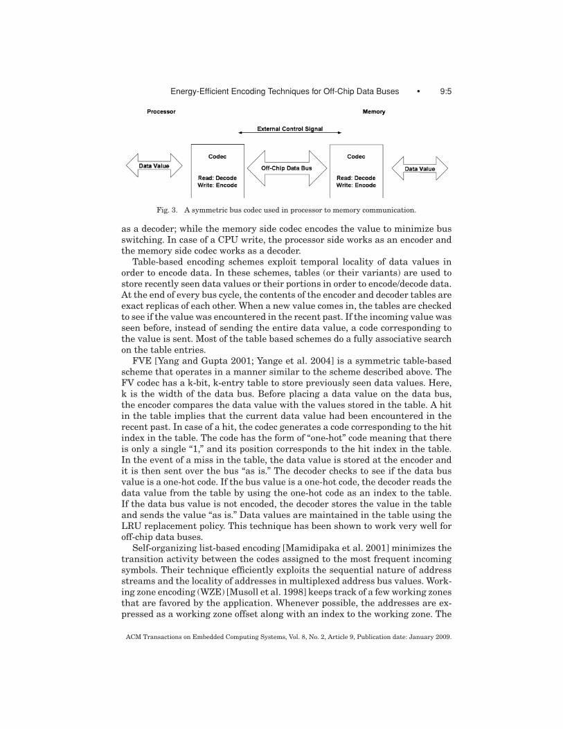
Figure 3 shows a symmetric pair of coders that are usually used for busencoding. An encoder/decoder (codec) is placed at the memory side and theprocessor side of the off-chip data bus. The codec decides whether the datavalue should be encoded or not before placing the value on the data bus. Whenthe codec encodes data values, it asserts a control signal to let the destinationknow that the current value is encoded and hence, it should not be interpreted“as is.” The codec design is symmetrical in nature to handle both read and writeoperations by the CPU. In case of a CPU read, the processor side codec works
ACM Transactions on Embedded Computing Systems, Vol. 8, No. 2, Article 9, Publication date: January 2009.
Energy-Efficient Encoding Techniques for Off-Chip Data Buses • 9:5
Fig. 3. A symmetric bus codec used in processor to memory communication.
as a decoder; while the memory side codec encodes the value to minimize busswitching. In case of a CPU write, the processor side works as an encoder andthe memory side codec works as a decoder.
Table-based encoding schemes exploit temporal locality of data values inorder to encode data. In these schemes, tables (or their variants) are used tostore recently seen data values or their portions in order to encode/decode data.At the end of every bus cycle, the contents of the encoder and decoder tables areexact replicas of each other. When a new value comes in, the tables are checkedto see if the value was encountered in the recent past. If the incoming value wasseen before, instead of sending the entire data value, a code corresponding tothe value is sent. Most of the table based schemes do a fully associative searchon the table entries.
FVE [Yang and Gupta 2001; Yange et al. 2004] is a symmetric table-basedscheme that operates in a manner similar to the scheme described above. TheFV codec has a k-bit, k-entry table to store previously seen data values. Here,k is the width of the data bus. Before placing a data value on the data bus,the encoder compares the data value with the values stored in the table. A hitin the table implies that the current data value had been encountered in therecent past. In case of a hit, the codec generates a code corresponding to the hitindex in the table. The code has the form of “one-hot” code meaning that thereis only a single “1,” and its position corresponds to the hit index in the table.In the event of a miss in the table, the data value is stored at the encoder andit is then sent over the bus “as is.” The decoder checks to see if the data busvalue is a one-hot code. If the bus value is a one-hot code, the decoder reads thedata value from the table by using the one-hot code as an index to the table.If the data bus value is not encoded, the decoder stores the value in the tableand sends the value “as is.” Data values are maintained in the table using theLRU replacement policy. This technique has been shown to work very well foroff-chip data buses.
Self-organizing list-based encoding [Mamidipaka et al. 2001] minimizes thetransition activity between the codes assigned to the most frequent incomingsymbols. Their technique efficiently exploits the sequential nature of addressstreams and the locality of addresses in multiplexed address bus values. Work-ing zone encoding (WZE) [Musoll et al. 1998] keeps track of a few working zonesthat are favored by the application. Whenever possible, the addresses are ex-pressed as a working zone offset along with an index to the working zone. The
ACM Transactions on Embedded Computing Systems, Vol. 8, No. 2, Article 9, Publication date: January 2009.
9:6 • D. C. Suresh et al.
encoder and decoder have a few registers to keep track of the working zonesand the index selects the current working zone’s value from one of the registers.They also extended the WZE scheme for data buses. The working zone offsetsare encoded using one-hot codes. However, this technique requires extra bitlines leading to redundancy in space.
LV et al. [2002] proposed a dictionary-based encoding scheme where in theupper few lines of the bus wires are kept in a high-impedance state and the lowerbits are encoded. While this scheme works well for large-sized caches, traceswith smaller cache sizes often tend to exhibit high entire data value locality.Hence, this scheme fails to exploit the occurrences of entire data values andconsequently, the reduction in switching activity is not significantly high. Weobserved that any scheme that exploits data value locality should be able toexploit entire as well as partial data value locality in order to achieve optimalenergy savings.
Our work differs from all of the aforementioned works in the following aspect.Our innovative schemes exploit value locality in full-width data streams as wellas partial-width data value streams. The most important difficulty we solvedhere is not to increase the number of control signals outside the data bus.Our technique uses just one external control signal to indicate the presenceof encoded values on the data bus. Our encoding schemes are also capable ofmaintaining a larger history of data values than the maximum possible historylength in the FVE scheme and hence, our schemes have a higher probability ofencoding incoming data values in the presence of data locality.
3. PARTIAL- AND FULL-WIDTH DATA BUS ENCODING SCHEMES
In this section, we describe the following three low-power bus-encoding tech-niques for efficient processor to memory communication.
—FV-i encoding: It is an extension to the FVE scheme [Yang and Gupta 2001].It encodes entire data values and uses just one external control signal toencode more values than the original FVE.
—FV-i-MSB-j encoding: encodes entire data values or the K-Most significantbits of data values (K is fixed by the designer).
We would first describe the high-level design methodologies including how toimplement a larger value history table size, how to incorporate MSB and LSBvalues and how the data correlation/decorrelation is done. We then elaborateeach technique and its variations in detail.
3.1 Design Methodologies
3.1.1 Increasing the Table Size. The FVE scheme sends a one-hot code fora data value, if it is contained in the frequent value table. However, the sizeof the frequent value table has the following limitation: For a k-bit wide databus, the number of entries stored in the frequent value table cannot exceedk. Consequently, a value can be encoded only if it is contained in the k-stored
ACM Transactions on Embedded Computing Systems, Vol. 8, No. 2, Article 9, Publication date: January 2009.
Energy-Efficient Encoding Techniques for Off-Chip Data Buses • 9:7
entries. By storing more than k entries, one has a higher probability of encodingan incoming data value. However, if we try to encode more values within theframework provided by the FVE scheme, we would require additional externalcontrol signals.
Control signals require the availability of a free pin on the chip and are,hence, very expensive to provide. So, we propose a framework that does notincrease the number of control signals required by the original FVE (which isone) when we increase the table size. However, increasing the table size doesrequire more number of control signals. The trick is to utilize portion of databus wires as control signals. For the remainder of this article, we will refer tothese data bus wires as internal control signals. If the enlarged table size isa multiple of the base table size, the internal control signals can serve as theindex to the different portion in the table. For example, a double-sized tableneeds only one internal control signal to indicate whether the code is generatedfrom the first half or the second half of the table. In this case, the internalcontrol signal reduces the effective base encoding table size by one. The nextquestion is what portion of the data bus should be selected as internal controlsignals. Through our experiments, we found that the transition activity in thelower-order bits of the data bus is often slightly higher than the activity inthe high order bits. Hence, while sending encoded values, we choose to make theleast significant bits as control signals. By doing so, they would not contributemuch to the total switching. In summary, our proposed method for increasingthe table size can be put formally as follows:
Consider a k-bit wide data bus. In order to keep a history of more than k,k-bit values, the number of entries stored in the table is of the form (k – m) ×2m, where m represents the number of internal control signals. Using the firstk − m lines, we send a one hot code corresponding to i mod (k-m) where i is thehit index in the enlarged frequent table. The last m lines, along with the indextransmitted on the bus, are used to specify the position of the data within thetable. For this scheme, the maximum number of transitions while sending anyencoded value is m + 1.
3.1.2 Bit-Width of Stored Values. As stated earlier, besides storing entiredata values, we also store the MSB and LSB portions of the data value inseparate tables. In order to determine the optimal width of the MSB and LSBentries, we varied the bit-width of the entries from 2 to 29 bits in steps of 1and observe the switching reduction for each case. The results are provided inSection 6. Since we encode table hits using one-hot code, the number of tableentries should be equal to the bit-width of the stored entries. However, as shownin Section 3.1.1, we can maintain more entries in the FV, MSB, and LSB tablesusing internal control signals.
3.1.3 Correlator/Decorrelator. We use a correlator/decorrelator in all ofour encoding schemes. At the encoder’s end, the correlator XORs, the cur-rent data value with the previous data bus value. The correlator’s output isplaced on the data bus. At the receiving end, decorrelator XORs, the currentand previous data bus value to obtain the current data value. Presence of a
ACM Transactions on Embedded Computing Systems, Vol. 8, No. 2, Article 9, Publication date: January 2009.
9:8 • D. C. Suresh et al.
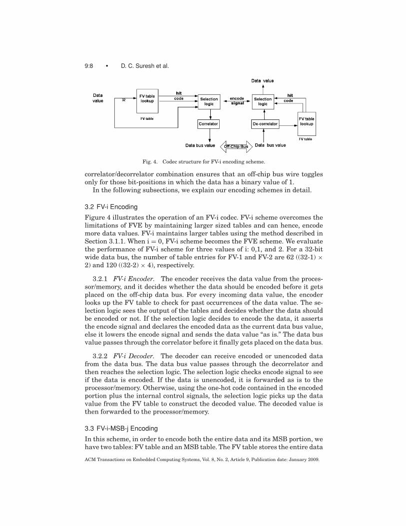
Fig. 4. Codec structure for FV-i encoding scheme.
correlator/decorrelator combination ensures that an off-chip bus wire togglesonly for those bit-positions in which the data has a binary value of 1.
In the following subsections, we explain our encoding schemes in detail.
3.2 FV-i Encoding
Figure 4 illustrates the operation of an FV-i codec. FV-i scheme overcomes thelimitations of FVE by maintaining larger sized tables and can hence, encodemore data values. FV-i maintains larger tables using the method described inSection 3.1.1. When i = 0, FV-i scheme becomes the FVE scheme. We evaluatethe performance of FV-i scheme for three values of i: 0,1, and 2. For a 32-bitwide data bus, the number of table entries for FV-1 and FV-2 are 62 ((32-1) ×2) and 120 ((32-2) × 4), respectively.
3.2.1 FV-i Encoder. The encoder receives the data value from the proces-sor/memory, and it decides whether the data should be encoded before it getsplaced on the off-chip data bus. For every incoming data value, the encoderlooks up the FV table to check for past occurrences of the data value. The se-lection logic sees the output of the tables and decides whether the data shouldbe encoded or not. If the selection logic decides to encode the data, it assertsthe encode signal and declares the encoded data as the current data bus value,else it lowers the encode signal and sends the data value “as is.” The data busvalue passes through the correlator before it finally gets placed on the data bus.
3.2.2 FV-i Decoder. The decoder can receive encoded or unencoded datafrom the data bus. The data bus value passes through the decorrelator andthen reaches the selection logic. The selection logic checks encode signal to seeif the data is encoded. If the data is unencoded, it is forwarded as is to theprocessor/memory. Otherwise, using the one-hot code contained in the encodedportion plus the internal control signals, the selection logic picks up the datavalue from the FV table to construct the decoded value. The decoded value isthen forwarded to the processor/memory.
3.3 FV-i-MSB-j Encoding
In this scheme, in order to encode both the entire data and its MSB portion, wehave two tables: FV table and an MSB table. The FV table stores the entire data
ACM Transactions on Embedded Computing Systems, Vol. 8, No. 2, Article 9, Publication date: January 2009.
Energy-Efficient Encoding Techniques for Off-Chip Data Buses • 9:9
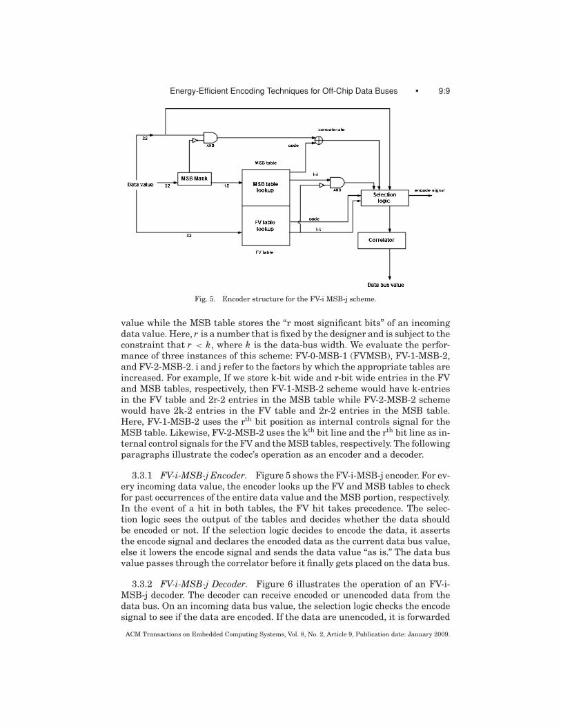
Fig. 5. Encoder structure for the FV-i MSB-j scheme.
value while the MSB table stores the “r most significant bits” of an incomingdata value. Here, r is a number that is fixed by the designer and is subject to theconstraint that r < k, where k is the data-bus width. We evaluate the perfor-mance of three instances of this scheme: FV-0-MSB-1 (FVMSB), FV-1-MSB-2,and FV-2-MSB-2. i and j refer to the factors by which the appropriate tables areincreased. For example, If we store k-bit wide and r-bit wide entries in the FVand MSB tables, respectively, then FV-1-MSB-2 scheme would have k-entriesin the FV table and 2r-2 entries in the MSB table while FV-2-MSB-2 schemewould have 2k-2 entries in the FV table and 2r-2 entries in the MSB table.Here, FV-1-MSB-2 uses the rth bit position as internal controls signal for theMSB table. Likewise, FV-2-MSB-2 uses the kth bit line and the rth bit line as in-ternal control signals for the FV and the MSB tables, respectively. The followingparagraphs illustrate the codec’s operation as an encoder and a decoder.
3.3.1 FV-i-MSB-j Encoder. Figure 5 shows the FV-i-MSB-j encoder. For ev-ery incoming data value, the encoder looks up the FV and MSB tables to checkfor past occurrences of the entire data value and the MSB portion, respectively.In the event of a hit in both tables, the FV hit takes precedence. The selec-tion logic sees the output of the tables and decides whether the data shouldbe encoded or not. If the selection logic decides to encode the data, it assertsthe encode signal and declares the encoded data as the current data bus value,else it lowers the encode signal and sends the data value “as is.” The data busvalue passes through the correlator before it finally gets placed on the data bus.
3.3.2 FV-i-MSB-j Decoder. Figure 6 illustrates the operation of an FV-i-MSB-j decoder. The decoder can receive encoded or unencoded data from thedata bus. On an incoming data bus value, the selection logic checks the encodesignal to see if the data are encoded. If the data are unencoded, it is forwarded
ACM Transactions on Embedded Computing Systems, Vol. 8, No. 2, Article 9, Publication date: January 2009.
9:10 • D. C. Suresh et al.
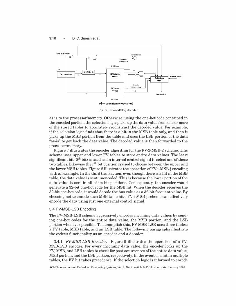
Fig. 6. FV-i-MSB-j decoder.
as is to the processor/memory. Otherwise, using the one-hot code contained inthe encoded portion, the selection logic picks up the data value from one or moreof the stored tables to accurately reconstruct the decoded value. For example,if the selection logic finds that there is a hit in the MSB table only, and then itpicks up the MSB portion from the table and uses the LSB portion of the data“as-is” to get back the data value. The decoded value is then forwarded to theprocessor/memory.
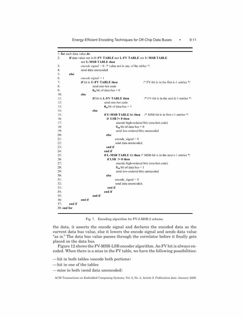
Figure 7 illustrates the encoder algorithm for the FV-2-MSB-2 scheme. Thisscheme uses upper and lower FV tables to store entire data values. The leastsignificant bit (0th bit) is used as an internal control signal to select one of thesetwo tables. Likewise the rth bit position is used to choose between the upper andthe lower MSB tables. Figure 8 illustrates the operation of FV-i-MSB-j encodingwith an example. In the third transaction, even though there is a hit in the MSBtable, the data value is sent unencoded. This is because the lower portion of thedata value is zero in all of its bit positions. Consequently, the encoder wouldgenerate a 32-bit one-hot code for the MSB hit. When the decoder receives the32-bit one-hot code, it would decode the bus value as a 32-bit frequent value. Bychoosing not to encode such MSB table hits, FV-i-MSB-j scheme can effectivelyencode the data using just one external control signal.
3.4 FV-MSB-LSB Encoding
The FV-MSB-LSB scheme aggressively encodes incoming data values by send-ing one-hot codes for the entire data value, the MSB portion, and the LSBportion whenever possible. To accomplish this, FV-MSB-LSB uses three tables:a FV table, MSB table, and an LSB table. The following paragraphs illustratethe codec’s functionality as an encoder and a decoder.
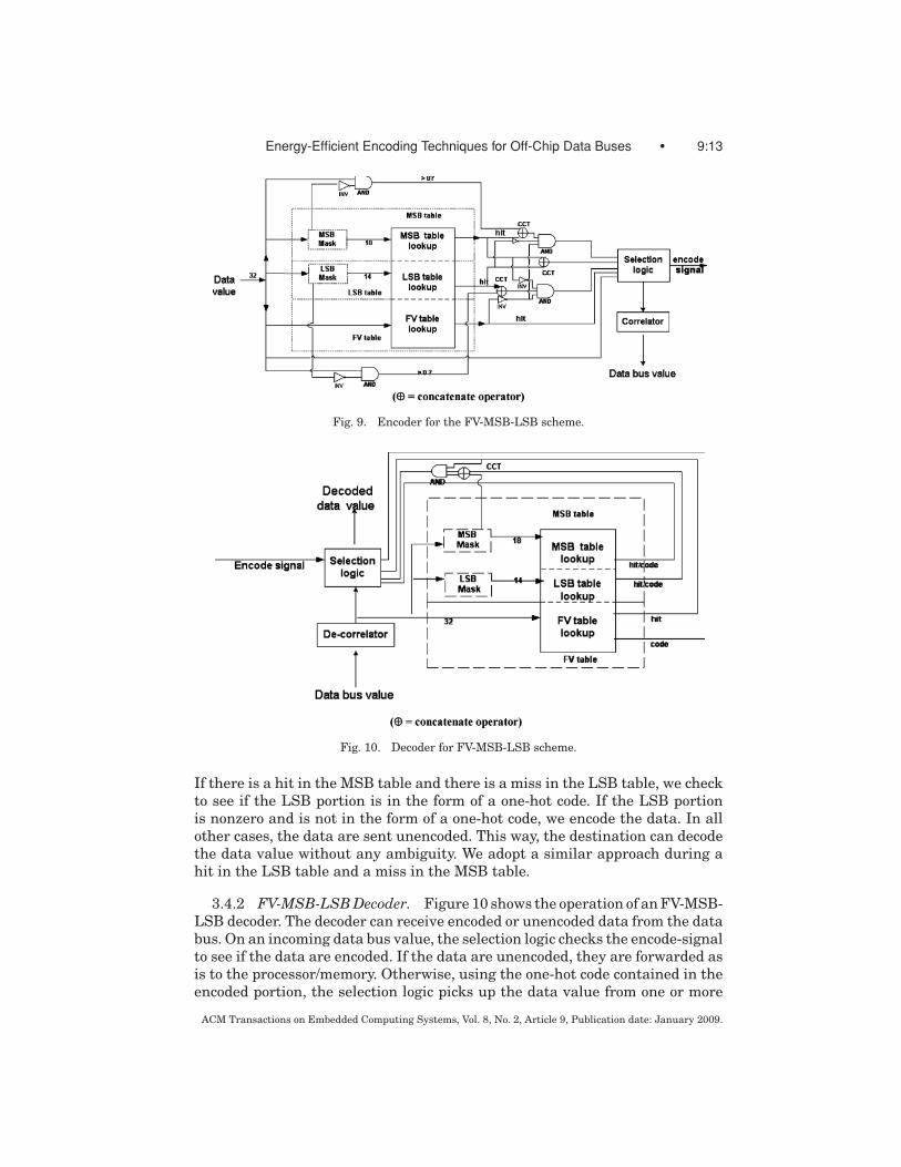
3.4.1 FV-MSB-LSB Encoder. Figure 9 illustrates the operation of a FV-MSB-LSB encoder. For every incoming data value, the encoder looks up theFV, MSB, and LSB tables to check for past occurrences of the entire data value,MSB portion, and the LSB portion, respectively. In the event of a hit in multipletables, the FV hit takes precedence. If the selection logic is informed to encode
ACM Transactions on Embedded Computing Systems, Vol. 8, No. 2, Article 9, Publication date: January 2009.
Energy-Efficient Encoding Techniques for Off-Chip Data Buses • 9:11
Fig. 7. Encoding algorithm for FV-2-MSB-2 scheme.
the data, it asserts the encode signal and declares the encoded data as thecurrent data bus value, else it lowers the encode signal and sends data value“as is.” The data bus value passes through the correlator before it finally getsplaced on the data bus.
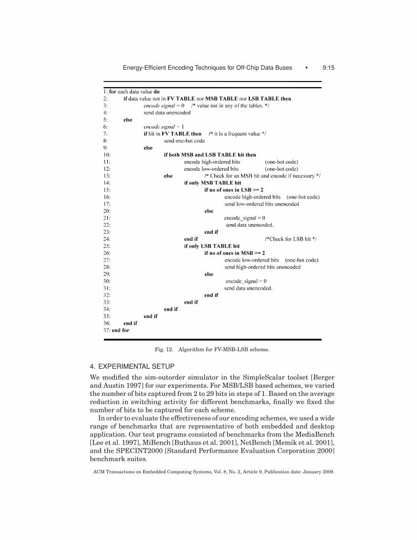
Figure 12 shows the FV-MSB-LSB encoder algorithm. An FV hit is always en-coded. When there is a miss in the FV table, we have the following possibilities:
—hit in both tables (encode both portions)
—hit in one of the tables
—miss in both (send data unencoded)
ACM Transactions on Embedded Computing Systems, Vol. 8, No. 2, Article 9, Publication date: January 2009.
9:12 • D. C. Suresh et al.
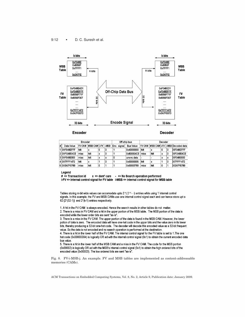
Fig. 8. FV-i-MSB-j. An example. FV and MSB tables are implemented as content-addressable
memories (CAMs).
ACM Transactions on Embedded Computing Systems, Vol. 8, No. 2, Article 9, Publication date: January 2009.
Energy-Efficient Encoding Techniques for Off-Chip Data Buses • 9:13
Fig. 9. Encoder for the FV-MSB-LSB scheme.
Fig. 10. Decoder for FV-MSB-LSB scheme.
If there is a hit in the MSB table and there is a miss in the LSB table, we checkto see if the LSB portion is in the form of a one-hot code. If the LSB portionis nonzero and is not in the form of a one-hot code, we encode the data. In allother cases, the data are sent unencoded. This way, the destination can decodethe data value without any ambiguity. We adopt a similar approach during ahit in the LSB table and a miss in the MSB table.
3.4.2 FV-MSB-LSB Decoder. Figure 10 shows the operation of an FV-MSB-LSB decoder. The decoder can receive encoded or unencoded data from the databus. On an incoming data bus value, the selection logic checks the encode-signalto see if the data are encoded. If the data are unencoded, they are forwarded asis to the processor/memory. Otherwise, using the one-hot code contained in theencoded portion, the selection logic picks up the data value from one or more
ACM Transactions on Embedded Computing Systems, Vol. 8, No. 2, Article 9, Publication date: January 2009.
9:14 • D. C. Suresh et al.
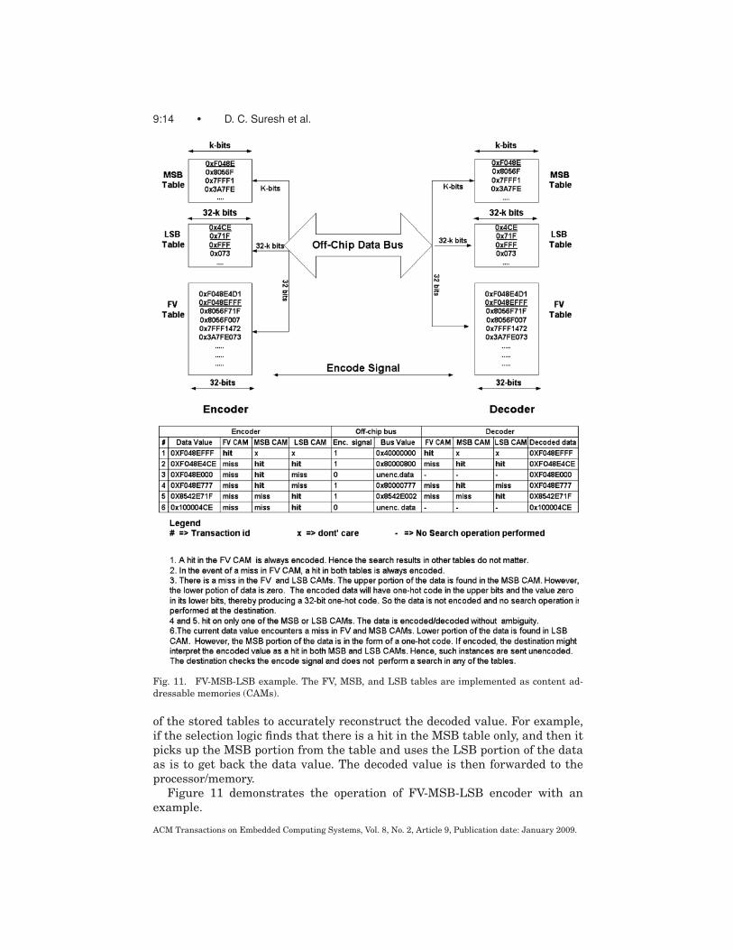
Fig. 11. FV-MSB-LSB example. The FV, MSB, and LSB tables are implemented as content ad-
dressable memories (CAMs).
of the stored tables to accurately reconstruct the decoded value. For example,if the selection logic finds that there is a hit in the MSB table only, and then itpicks up the MSB portion from the table and uses the LSB portion of the dataas is to get back the data value. The decoded value is then forwarded to theprocessor/memory.
Figure 11 demonstrates the operation of FV-MSB-LSB encoder with anexample.
ACM Transactions on Embedded Computing Systems, Vol. 8, No. 2, Article 9, Publication date: January 2009.
Energy-Efficient Encoding Techniques for Off-Chip Data Buses • 9:15
Fig. 12. Algorithm for FV-MSB-LSB scheme.
4. EXPERIMENTAL SETUP
We modified the sim-outorder simulator in the SimpleScalar toolset [Bergerand Austin 1997] for our experiments. For MSB/LSB based schemes, we variedthe number of bits captured from 2 to 29 bits in steps of 1. Based on the averagereduction in switching activity for different benchmarks, finally we fixed thenumber of bits to be captured for each scheme.
In order to evaluate the effectiveness of our encoding schemes, we used a widerange of benchmarks that are representative of both embedded and desktopapplication. Our test programs consisted of benchmarks from the MediaBench[Lee et al. 1997], MiBench [Buthaus et al. 2001], NetBench [Memik et al. 2001],and the SPECINT2000 [Standard Performance Evaluation Corporation 2000]benchmark suites.
ACM Transactions on Embedded Computing Systems, Vol. 8, No. 2, Article 9, Publication date: January 2009.
9:16 • D. C. Suresh et al.
Fig. 13. Average reduction in switching activity for varying MSB lengths.
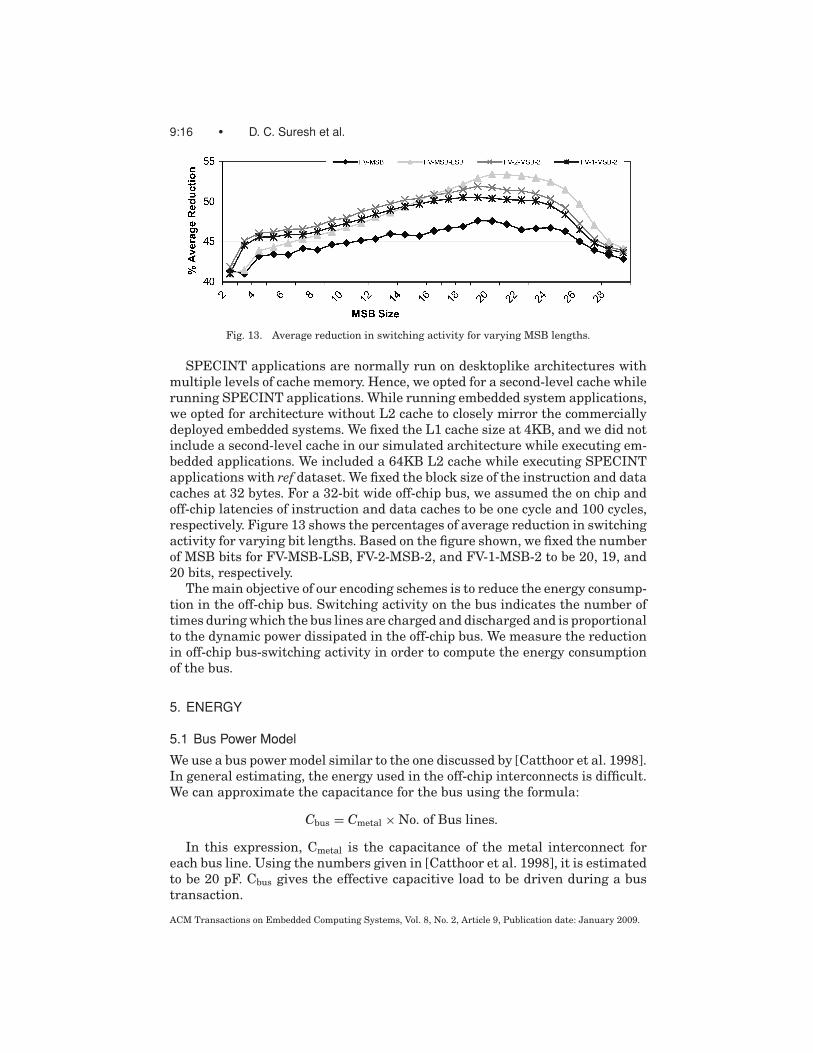
SPECINT applications are normally run on desktoplike architectures withmultiple levels of cache memory. Hence, we opted for a second-level cache whilerunning SPECINT applications. While running embedded system applications,we opted for architecture without L2 cache to closely mirror the commerciallydeployed embedded systems. We fixed the L1 cache size at 4KB, and we did notinclude a second-level cache in our simulated architecture while executing em-bedded applications. We included a 64KB L2 cache while executing SPECINTapplications with ref dataset. We fixed the block size of the instruction and datacaches at 32 bytes. For a 32-bit wide off-chip bus, we assumed the on chip andoff-chip latencies of instruction and data caches to be one cycle and 100 cycles,respectively. Figure 13 shows the percentages of average reduction in switchingactivity for varying bit lengths. Based on the figure shown, we fixed the numberof MSB bits for FV-MSB-LSB, FV-2-MSB-2, and FV-1-MSB-2 to be 20, 19, and20 bits, respectively.
The main objective of our encoding schemes is to reduce the energy consump-tion in the off-chip bus. Switching activity on the bus indicates the number oftimes during which the bus lines are charged and discharged and is proportionalto the dynamic power dissipated in the off-chip bus. We measure the reductionin off-chip bus-switching activity in order to compute the energy consumptionof the bus.
5. ENERGY
5.1 Bus Power Model
We use a bus power model similar to the one discussed by [Catthoor et al. 1998].In general estimating, the energy used in the off-chip interconnects is difficult.We can approximate the capacitance for the bus using the formula:
Cbus = Cmetal × No. of Bus lines.
In this expression, Cmetal is the capacitance of the metal interconnect foreach bus line. Using the numbers given in [Catthoor et al. 1998], it is estimatedto be 20 pF. Cbus gives the effective capacitive load to be driven during a bustransaction.
ACM Transactions on Embedded Computing Systems, Vol. 8, No. 2, Article 9, Publication date: January 2009.
Energy-Efficient Encoding Techniques for Off-Chip Data Buses • 9:17
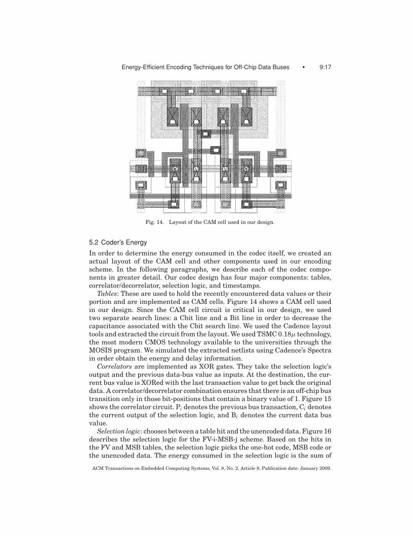
Fig. 14. Layout of the CAM cell used in our design.
5.2 Coder’s Energy
In order to determine the energy consumed in the codec itself, we created anactual layout of the CAM cell and other components used in our encodingscheme. In the following paragraphs, we describe each of the codec compo-nents in greater detail. Our codec design has four major components: tables,correlator/decorrelator, selection logic, and timestamps.
Tables: These are used to hold the recently encountered data values or theirportion and are implemented as CAM cells. Figure 14 shows a CAM cell usedin our design. Since the CAM cell circuit is critical in our design, we usedtwo separate search lines: a Cbit line and a Bit line in order to decrease thecapacitance associated with the Cbit search line. We used the Cadence layouttools and extracted the circuit from the layout. We used TSMC 0.18μ technology,the most modern CMOS technology available to the universities through theMOSIS program. We simulated the extracted netlists using Cadence’s Spectrain order obtain the energy and delay information.
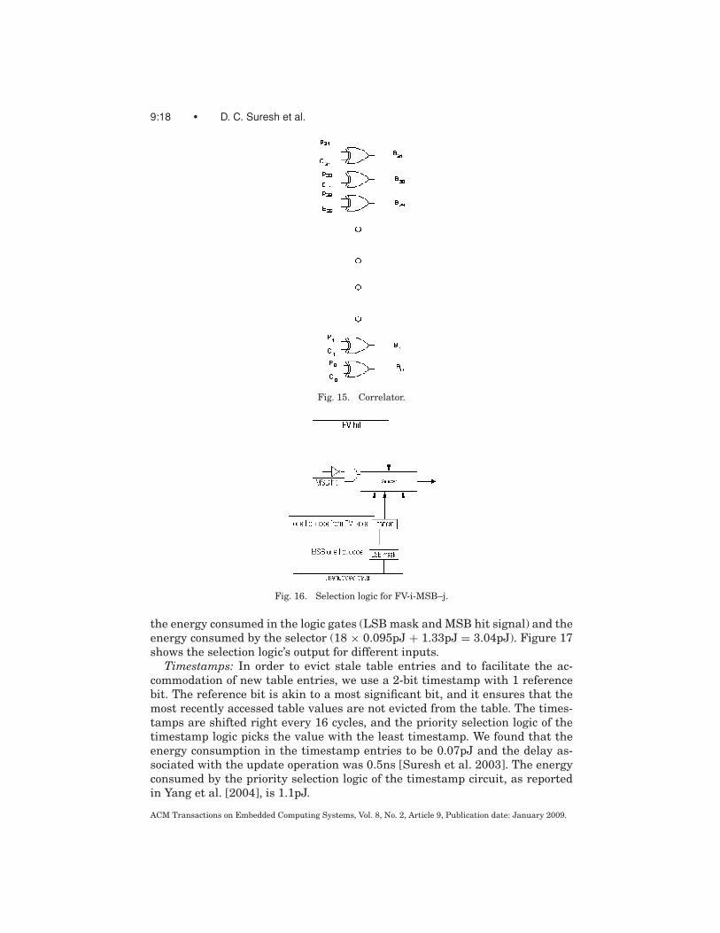
Correlators are implemented as XOR gates. They take the selection logic’soutput and the previous data-bus value as inputs. At the destination, the cur-rent bus value is XORed with the last transaction value to get back the originaldata. A correlator/decorrelator combination ensures that there is an off-chip bustransition only in those bit-positions that contain a binary value of 1. Figure 15shows the correlator circuit. Pi denotes the previous bus transaction, Ci denotesthe current output of the selection logic, and Bi denotes the current data busvalue.
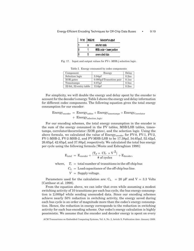
Selection logic: chooses between a table hit and the unencoded data. Figure 16describes the selection logic for the FV-i-MSB-j scheme. Based on the hits inthe FV and MSB tables, the selection logic picks the one-hot code, MSB code orthe unencoded data. The energy consumed in the selection logic is the sum of
ACM Transactions on Embedded Computing Systems, Vol. 8, No. 2, Article 9, Publication date: January 2009.
9:18 • D. C. Suresh et al.
Fig. 15. Correlator.
Fig. 16. Selection logic for FV-i-MSB–j.
the energy consumed in the logic gates (LSB mask and MSB hit signal) and theenergy consumed by the selector (18 × 0.095pJ + 1.33pJ = 3.04pJ). Figure 17shows the selection logic’s output for different inputs.
Timestamps: In order to evict stale table entries and to facilitate the ac-commodation of new table entries, we use a 2-bit timestamp with 1 referencebit. The reference bit is akin to a most significant bit, and it ensures that themost recently accessed table values are not evicted from the table. The times-tamps are shifted right every 16 cycles, and the priority selection logic of thetimestamp logic picks the value with the least timestamp. We found that theenergy consumption in the timestamp entries to be 0.07pJ and the delay as-sociated with the update operation was 0.5ns [Suresh et al. 2003]. The energyconsumed by the priority selection logic of the timestamp circuit, as reportedin Yang et al. [2004], is 1.1pJ.
ACM Transactions on Embedded Computing Systems, Vol. 8, No. 2, Article 9, Publication date: January 2009.
Energy-Efficient Encoding Techniques for Off-Chip Data Buses • 9:19
Fig. 17. Input and output values for FV-i -MSB-j selection logic.
Table I. Energy consumed by codec components
Component Energy Delay
Selection logic 3.04pJ 0.2ns
XOR gates 0.095pJ/Transition pair 0.1ns
Timestamps 0.07pJ 0.5ns
32-bit, 32-entry table 13.6pJ 0.2ns
For simplicity, we will double the energy and delay spent by the encoder toaccount for the decoder’s energy. Table I shows the energy and delay informationfor different codec components. The following equation gives the total energyconsumption for our encoder:
For our encoding schemes, the total energy consumption in the encoder isthe sum of the energy consumed in the FV tables, MSB/LSB tables, times-tamps, correlator/decorrelator (XOR gates), and the selection logic. Using theabove formula, we calculated the value of Energyencoder for FV-0, FV-1, FV-2,FV-1-MSB-2, FV-2-MSB-2, and FV-MSB-LSB to be 17.38pJ, 34.65pJ, 52.42pJ,26.65pJ, 42.65pJ, and 37.88pJ, respectively. We calculated the total bus energyper cycle using the following formula [Weste and Eshraghian 1998]:
Etotal = Eencoder + {Tr × CL × V 2}# of cycles
+ Edecoder,
where, Tr = total number of transitions in the off-chip bus
CL = Load capacitance of the off-chip bus line.
V = Supply voltage.
Parameters used for the calculation are: CL = 20 pF and V = 3.3 Volts[Catthoor et al. 1998].
From the equation above, we can infer that even while assuming a modestswitching activity of 10 transitions per each bus cycle, the bus energy consump-tion is 2,000pJ while sending unencoded data. Since our encoding schemesachieve nearly 50% reduction in switching activity, the energy saved duringeach bus cycle is an order of magnitude more than the codec’s energy consump-tion. Hence, the reduction in energy corresponds to the reduction in switchingactivity for each bus-encoding scheme. Our codec’s energy calculation is highlypessimistic. We assume that the encoder and decoder energy is spent on every
ACM Transactions on Embedded Computing Systems, Vol. 8, No. 2, Article 9, Publication date: January 2009.
9:20 • D. C. Suresh et al.
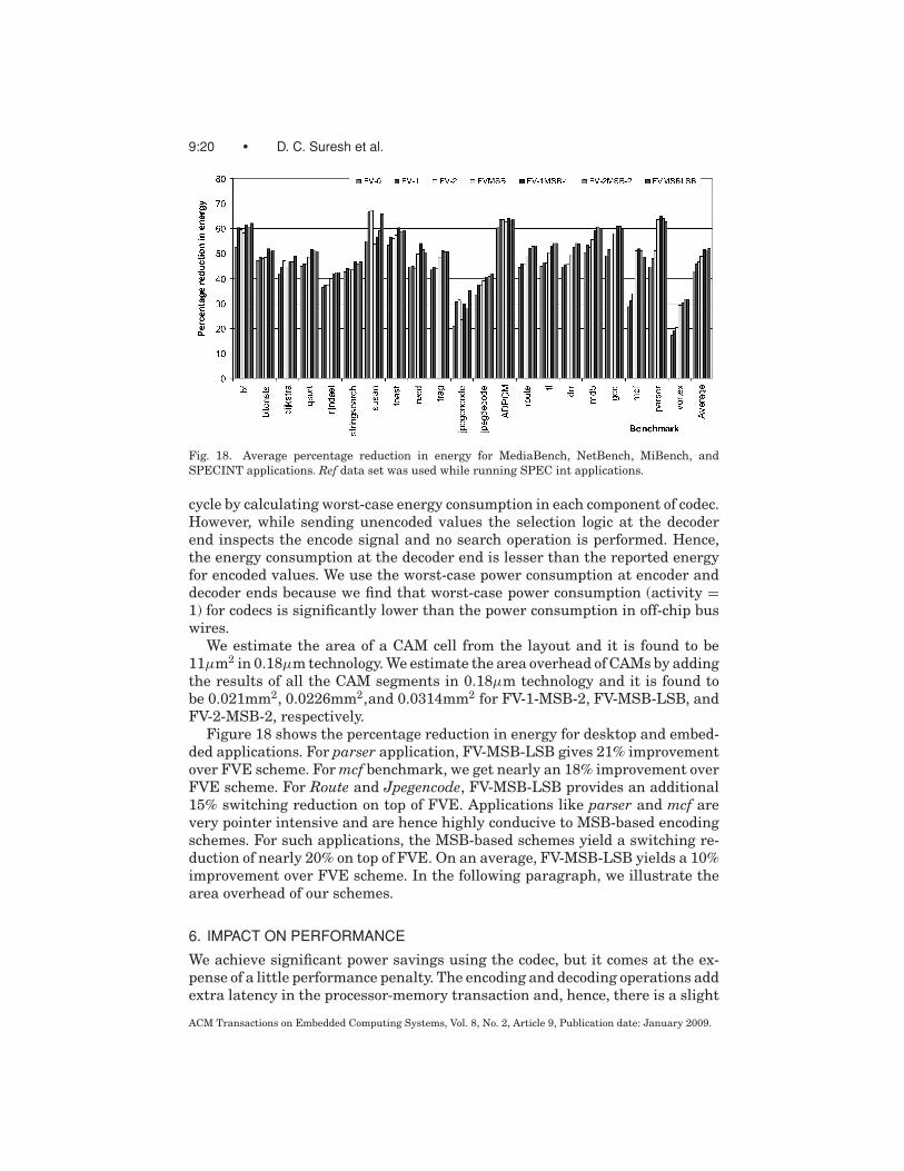
Fig. 18. Average percentage reduction in energy for MediaBench, NetBench, MiBench, and
SPECINT applications. Ref data set was used while running SPEC int applications.
cycle by calculating worst-case energy consumption in each component of codec.However, while sending unencoded values the selection logic at the decoderend inspects the encode signal and no search operation is performed. Hence,the energy consumption at the decoder end is lesser than the reported energyfor encoded values. We use the worst-case power consumption at encoder anddecoder ends because we find that worst-case power consumption (activity =1) for codecs is significantly lower than the power consumption in off-chip buswires.
We estimate the area of a CAM cell from the layout and it is found to be11μm2 in 0.18μm technology. We estimate the area overhead of CAMs by addingthe results of all the CAM segments in 0.18μm technology and it is found tobe 0.021mm2, 0.0226mm2,and 0.0314mm2 for FV-1-MSB-2, FV-MSB-LSB, andFV-2-MSB-2, respectively.
Figure 18 shows the percentage reduction in energy for desktop and embed-ded applications. For parser application, FV-MSB-LSB gives 21% improvementover FVE scheme. For mcf benchmark, we get nearly an 18% improvement overFVE scheme. For Route and Jpegencode, FV-MSB-LSB provides an additional15% switching reduction on top of FVE. Applications like parser and mcf arevery pointer intensive and are hence highly conducive to MSB-based encodingschemes. For such applications, the MSB-based schemes yield a switching re-duction of nearly 20% on top of FVE. On an average, FV-MSB-LSB yields a 10%improvement over FVE scheme. In the following paragraph, we illustrate thearea overhead of our schemes.
6. IMPACT ON PERFORMANCE
We achieve significant power savings using the codec, but it comes at the ex-pense of a little performance penalty. The encoding and decoding operations addextra latency in the processor-memory transaction and, hence, there is a slight
ACM Transactions on Embedded Computing Systems, Vol. 8, No. 2, Article 9, Publication date: January 2009.
Energy-Efficient Encoding Techniques for Off-Chip Data Buses • 9:21
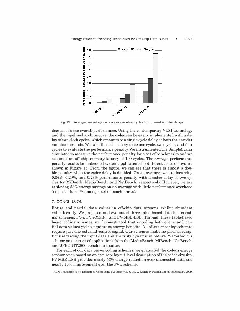
Fig. 19. Average percentage increase in execution cycles for different encoder delays.
decrease in the overall performance. Using the contemporary VLSI technologyand the pipelined architecture, the codec can be easily implemented with a de-lay of two clock cycles, which amounts to a single cycle delay at both the encoderand decoder ends. We take the codec delay to be one cycle, two cycles, and fourcycles to evaluate the performance penalty. We instrumented the SimpleScalarsimulator to measure the performance penalty for a set of benchmarks and weassumed an off-chip memory latency of 100 cycles. The average performancepenalty results for embedded system applications for different codec delays areshown in Figure 15. From the figure, we can see that there is almost a dou-ble penalty when the codec delay is doubled. On an average, we are incurring0.06%, 0.29%, and 0.76% performance penalty with a codec delay of two cy-cles for MiBench, MediaBench, and NetBench, respectively. However, we areachieving 53% energy savings on an average with little performance overhead(i.e., less than 1% among a set of benchmarks).
7. CONCLUSION
Entire and partial data values in off-chip data streams exhibit abundantvalue locality. We proposed and evaluated three table-based data bus encod-ing schemes: FV-i, FV-i-MSB-j, and FV-MSB-LSB. Through these table-basedbus-encoding schemes, we demonstrated that encoding both entire and par-tial data values yields significant energy benefits. All of our encoding schemesrequire just one external control signal. Our schemes make no prior assump-tions regarding the input data and are truly dynamic in nature. We tested ourscheme on a subset of applications from the MediaBench, MiBench, NetBench,and SPECINT2000 benchmark suites.
For each of our data bus-encoding schemes, we evaluated the codec’s energyconsumption based on an accurate layout-level description of the codec circuits.FV-MSB-LSB provides nearly 53% energy reduction over unencoded data andnearly 10% improvement over the FVE scheme.
ACM Transactions on Embedded Computing Systems, Vol. 8, No. 2, Article 9, Publication date: January 2009.
9:22 • D. C. Suresh et al.
REFERENCES
BASU, K., CHOUDHARY, A., PISHARATH, J., AND M. KANDEMIR, M. 2002. Power protocol: Reducing power
dissipation on off-chip data buses. In Proceedings of the 35th Annual IEEE/ACM Symposium onMicro Architecture (MICRO-35). IEEE, Los Alamitos, CA.
BENINI, L., MACCI, A., MACCI, E., PONCINO, M., AND SCARSI, R. 2000. Architectures and synthesis
algorithms for power efficient bus interfaces. IEEE Trans. Comput. Aid. Des. Circ. Syst. 19, 9.
BENINI, L, DE MICHELI, G., MACCI, E., SCUITO, D., AND SILVANO, C. 1997. Asymptotic zero-transition
activity encoding for address buses in low-power microprocessor-bases systems. In Proceedingsof the 7th Great Lakes VLSI Symposium, IEEE, Los Alamitos, CA, 77–82.
BURGER D. AND AUSTIN T. 1997. The SimpleScalar tool set, version 2.0. Tech. rep. University of
Wisconsin-Madison.
CATTHOOR, E., WUYTACK, S., DE GREF, E., BALASA, F., NACHTERGAELE, L., AND VANDECAPPELLE, A. 1998.
Exploration of Memory Organization for Embedded Multimedia System Design. Springer, Berlin,
Germany.
CHERN, J. H., JURANG, J., ARLEDGE, L., LI, P., AND YANG, P. 1992. Multi-level metal capacitance
models for CAD design. IEEE Electron Device Lett. 13, 32–34.
CITRON, D. AND RUDOLPH, L. 1995. Creating a wider bus using caching techniques. In Proceed-ings of the 1stInternational Symposium on High Performance Computer Architecture. IEEE, Los
Alamitos, CA, 90–99.
FARRENS, M. AND PARK, A. 1991. Dynamic base register caching: a technique for reducing address
bus width. In Proceedings of 18th International Symposium on Computer Architecture (ISCA).IEEE, Los Alamitos, CA, 128–137.
GIVARGIS, T. AND VAHID, F. 1998. Interface exploration for reduced power in core-based systems.
In Proceedings of the 11th International Symposium on System Synthesis. IEEE, Los Alamitos,
CA.
GIVARGIS, T. AND EPPSTEIN, D. 2002. Reference-caching using unit distance redundant codes for ac-
tivity reduction on address buses. In Proceedings of the 8th International Workshop on EmbeddedHardware/Software Codesign (ESCODES’02). IEEE, Los Alamitos, CA.
GUTHAUS, M. R, RINGENBERG, J. S., ERNST, D., AUSTIN, T. M., MUDGE, T., AND BROWN, R. 2001.
MiBench: a free, commercially representative embedded benchmark suite. In Proceedings ofthe 4th Annual Workshop on Workload Characterization. IEEE, Los Alamitos, CA.
HSIAO, I. Y. L., WANG, D. H., AND JEN, C. W. 2001. Power modeling and low-power design of content
addressable memories. In Proceedings of the IEEE International Symposium on Circuits andSystems (ISCAS’01). IEEE, Los Alamitos, CA, 926–929.
KOMATSU, S., IKEDA, M., AND ASADA, K. 1999. Low power chip interface based on bus data encoding
with adaptive code-book method. In Proceedings of the 9th Great Lakes Symposium on VLSI.IEEE, Los Alamitos, CA, 368.
LEE, C., POTKONJAK, M., AND MANGIONE SMITH, W. 1997. MediaBench: a tool for evaluating and
synthesizing multimedia and communications systems”, In Proceedings of the 30th Annual In-ternational Symposium on Microarchitecture (MICRO-30), IEEE, Los Alamitos, CA, 330–335.
LV, T., HENKEL, J., LEKATSAS, H., AND WOLF, W. 2002. An adaptive dictionary encoding scheme
for SOC data buses. In Proceedings of the Design Automation and Test in Europe. IEEE, Los
Alamitos, CA.
MAMIDIPAKA, M., HIRSCHBERG, D., AND DUTT, N. 2001. Low power address bus encoding using self-
organizing lists. In Proceedings of the International Symposium on Low Power Design. IEEE, Los
Alamitos, CA, 188–193.
MEMIK, G., MANGIONE SMITH, W. H., AND HU, W. 2001. NetBench: a benchmarking suite for net-
work processors. In Proceedings of the International Conference on Computer Aided Design(ICCAD2001). IEEE, Los Alamitos, CA, 39–42.
MUSOLL, E., LANG, T., AND CORTADELLA, J. 1998. Working zone encoding for reducing the energy in
SEMICONDUCTOR INDUSTRY ASSOCIATION (SIA). 2003. National technology roadmap for semiconductors
(NTRS). SIA, San Jose, CA.
RAGHUNATHAN, A., JHA, N. K., AND DEY, S. 1998. High-Level Power Analysis and Optimization.
Kluwer Academic Publishers, Norwell, MA.
ACM Transactions on Embedded Computing Systems, Vol. 8, No. 2, Article 9, Publication date: January 2009.
Energy-Efficient Encoding Techniques for Off-Chip Data Buses • 9:23
RAMPRASAD, S., SHAMBAG, N. R., AND HAJJ, I. N. 1999. A coding framework for low power address
and data buses. IEEE Trans. VLSI Syst. 7, 212–221.
STANDARD PERFORMANCE EVALUATION CORPORATION. 2000. SPEC CPU2000 V1.3. http://www.
specbench.org/cpu2000.
SU, C. L., TSUI, C. Y., AND DESPAIN, A. M. 1994. Saving power in the control path of embedded
processors. IEEE Des. Test Comput. 11, 24–30, Volume 11, 1994.
STAN M. R. AND BURLESON, W. P. 1995. Bus-invert coding for low power I/O. IEEE Trans. LargeVLSI Syst., 3, 49–58.
SURESH, D. C., YANG, J., ZHANG, C., AGRAWAL, B., AND NAJJAR, W. 2003. FV-MSB: A scheme to reduce
transition activity on data buses. In Proceedings of the 10th Annual International Conference onHigh Performance Computing. Springer, Berlin, Germany.
VICTOR, B. M. AND KEUTZER, K. 2001. Bus encoding to prevent crosstalk delay. In Proceeding ofthe International Conference on Computer-Aided Design (ICCAD).
WESTE, N. H. E. AND ESHRAGHIAN, K. 1998. Principles of CMOS VSLI Design. Addison Wesley.
YANG, J. AND GUPTA, R. 2001. FV encoding for low power data I/O. In Proceedings of the Interna-tional Symposium on Low Power Electronic Design. IEEE, Los Alamitos, CA, 84–87.
YANG, J., GUPTA, R., AND ZHANG, C. H. 2004. FV-encoding for low power data buses. ACM Trans.Des. Autom. Embed. Syst. 9, 3, 354–384.
ZHANG, Y., YANG, J., AND GUPTA, R. 2000. Frequent value locality and value-centric data cache
design. In Proceedings of the 9th International Conference on Architectural Support for Program-ming Languages and Operating Systems (ASPLOS–IX). ACM, New York, 150–159.
Received September 2004; revised February 2006, July 2006, May 2008; accepted August 2008
ACM Transactions on Embedded Computing Systems, Vol. 8, No. 2, Article 9, Publication date: January 2009.