• 0.1% typical measurement error over 500:1 dynamic range (MCP3905)
• 0.1% typical measurement error over 1000:1 dynamic range (MCP3906)
• Programmable Gain Amplifier (PGA) for small-signal inputs supports low-value shunt current sensor- 16:1 PGA - MCP3905- 32:1 PGA - MCP3906
• Ultra-low drift on-chip reference: 15 ppm/°C (typ.)• Direct drive for electromagnetic mechanical
counter and two-phase stepper motors• Low IDD of 4 mA (typ.)
• Tamper output pin for negative power indication• Industrial Temperature Range: -40°C to +85°C• Supplies instantaneous active (real) power on
HFOUT for meter calibration
US Patents Pending
DescriptionThe MCP3905/06 devices are energy-metering ICsdesigned to support the IEC 62053 InternationalMetering Standard Specification. They supply afrequency output proportional to the average active(real) power, as well as a higher-frequency outputproportional to the instantaneous power for metercalibration. They include two 16-bit, delta-sigma ADCsfor a wide range of IB and IMAX currents and/or smallshunt (< 200 µOhms) meter designs. It includes anultra-low drift voltage reference with < 15 ppm/°Cthrough a specially designed band gap temperaturecurve for the minimum gradient across the industrialtemperature range. A fixed-function DSP block is on-chip for active (real) power calculation. Strong outputdrive for mechanical counters are on-chip to reducefield failures and mechanical counter sticking. A no-load threshold block prevents any current creep mea-surements. A Power-On Reset (POR) block restrictsmeter performance during low-voltage situations.These accurate energy-metering ICs with high fieldreliability are available in the industry-standard pinout.
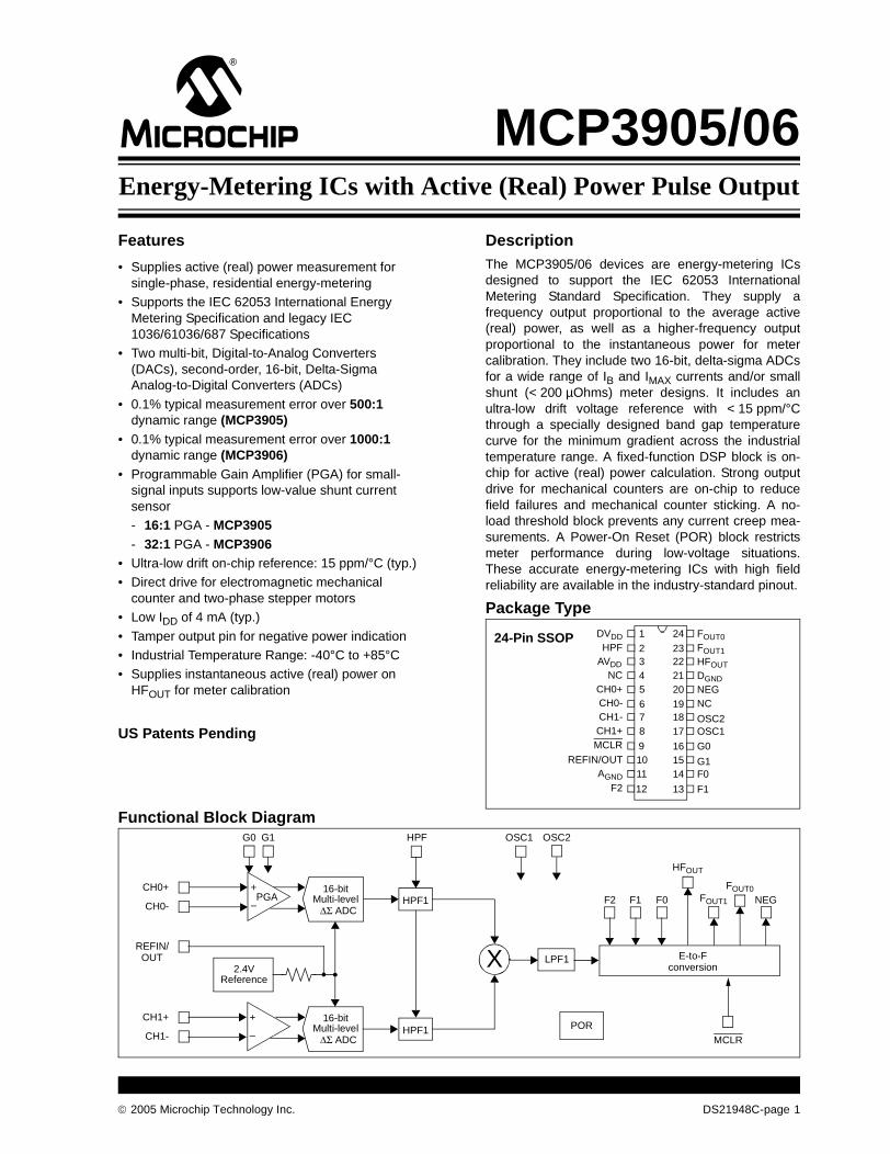
Package Type
Functional Block Diagram
FOUT0
DGNDNEG
1
234
24
23222120191817
5
678
FOUT1
NC
OSC2OSC1
DVDDHPF
AVDDNC
CH0+CH0-CH1-CH1+
HFOUT
169 G0MCLR
1514
1011
G1F0
REFIN/OUTAGND
1312 F1F2
24-Pin SSOP
16-bit
ΔΣ ADC
MCLR
+
–
CH0+
CH0-
Reference2.4V
+
–
CH1+
CH1-
HPF1
LPF1 E-to-Fconversion
REFIN/
FOUT1
HFOUT
G0 G1
F2 F1FOUT0
OSC1 OSC2
OUT
NEG
HPF
F0Multi-level
16-bit
ΔΣ ADCMulti-level
X
HPF1
PGA
POR
Energy-Metering ICs with Active (Real) Power Pulse Output
VDD ...................................................................................7.0VDigital inputs and outputs w.r.t. AGND........ -0.6V to VDD +0.6VAnalog input w.r.t. AGND ..................................... ....-6V to +6VVREF input w.r.t. AGND ............................... -0.6V to VDD +0.6VStorage temperature .....................................-65°C to +150°CAmbient temp. with power applied ................-65°C to +125°CSoldering temperature of leads (10 seconds) .............+300°CESD on the analog inputs (HBM,MM) .................5.0 kV, 500V
ESD on all other pins (HBM,MM) ........................5.0 kV, 500V
† Notice: Stresses above those listed under "MaximumRatings" may cause permanent damage to the device. This isa stress rating only and functional operation of the device atthose or any other conditions above those indicated in theoperation listings of this specification is not implied. Exposureto maximum rating conditions for extended periods may affectdevice reliability.
ELECTRICAL CHARACTERISTICSElectrical Specifications: Unless otherwise indicated, all parameters apply at AVDD = DVDD = 4.5V – 5.5V,Internal VREF, HPF turned on (AC mode), AGND, DGND = 0V, MCLK = 3.58 MHz; TA = -40°C to +85°C.
DC Power SupplyRejection Ratio(Output Frequency Variation)
DC PSRR — 0.01 — % FOUT HPF = 1, Gain = 1 (Note 3)
System Gain Error — 3 10 % FOUT Note 2, Note 5ADC/PGA SpecificationsOffset Error VOS — 2 5 mV Referred to Input
Gain Error Match — 0.5 — % FOUT Note 8Internal Voltage ReferenceVoltage — 2.4 — V
Tolerance — ±2 — %Tempco — 15 — ppm/°CNote 1: Measurement error = (Energy Measured By Device - True Energy)/True Energy * 100%. Accuracy is
measured with signal (±660 mV) on Channel 1. FOUT0, FOUT1 pulse outputs. Valid from 45 Hz to 65 Hz. See Section 2.0 “Typical Performance Curves” for higher frequencies and increased dynamic range.
2: Does not include internal VREF. Gain = 1, CH0 = 470 mVDC, CH1 = 660 mVDC, difference between measured output frequency and expected transfer function.
3: Percent of HFOUT output frequency variation; Includes external VREF = 2.5V, CH1 = 100 mVRMS @ 50 Hz, CH2 = 100 mVRMS @ 50 Hz, AVDD = 5V + 1Vpp @ 100 Hz. DC PSRR: 5V ±500 mV.
4: Error applies down to 60° lead (PF = 0.5 capacitive) and 60° lag (PF = 0.5 inductive).5: Refer to Section 4.0 “Device Overview” for complete description.
6: Specified by characterization, not production tested.7: 1 MCLK period at 3.58 MHz is equivalent to less than <0.005 degrees at 50 or 60 Hz.8: Gain error match is measured from CH0 G = 1 to any other gain setting.
Note: The MCP3905/06 operate over this extended temperature range, but with reduced performance. In anycase, the Junction Temperature (TJ) must not exceed the Absolute Maximum specification of +150°C.
ELECTRICAL CHARACTERISTICS (CONTINUED)Electrical Specifications: Unless otherwise indicated, all parameters apply at AVDD = DVDD = 4.5V – 5.5V,Internal VREF, HPF turned on (AC mode), AGND, DGND = 0V, MCLK = 3.58 MHz; TA = -40°C to +85°C.
Parameter Sym Min Typ. Max Units Comment
Note 1: Measurement error = (Energy Measured By Device - True Energy)/True Energy * 100%. Accuracy is measured with signal (±660 mV) on Channel 1. FOUT0, FOUT1 pulse outputs. Valid from 45 Hz to 65 Hz. See Section 2.0 “Typical Performance Curves” for higher frequencies and increased dynamic range.
2: Does not include internal VREF. Gain = 1, CH0 = 470 mVDC, CH1 = 660 mVDC, difference between measured output frequency and expected transfer function.
3: Percent of HFOUT output frequency variation; Includes external VREF = 2.5V, CH1 = 100 mVRMS @ 50 Hz, CH2 = 100 mVRMS @ 50 Hz, AVDD = 5V + 1Vpp @ 100 Hz. DC PSRR: 5V ±500 mV.
4: Error applies down to 60° lead (PF = 0.5 capacitive) and 60° lag (PF = 0.5 inductive).
5: Refer to Section 4.0 “Device Overview” for complete description.6: Specified by characterization, not production tested.7: 1 MCLK period at 3.58 MHz is equivalent to less than <0.005 degrees at 50 or 60 Hz.
8: Gain error match is measured from CH0 G = 1 to any other gain setting.
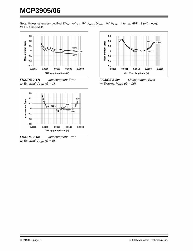
Note: The graphs and tables provided following this note are a statistical summary based on a limited number ofsamples and are provided for informational purposes only. The performance characteristics listed hereinare not tested or guaranteed. In some graphs or tables, the data presented may be outside the specifiedoperating range (e.g., outside specified power supply range) and therefore outside the warranted range.
3.0 PIN DESCRIPTIONSThe descriptions of the pins are listed in Table 3-1.
TABLE 3-1: PIN FUNCTION TABLE
3.1 Digital VDD (DVDD)
DVDD is the power supply pin for the digital circuitrywithin the MCP3905/06.
DVDD requires appropriate bypass capacitors andshould be maintained to 5V ±10% for specifiedoperation. Please refer to Section 5.0 “ApplicationsInformation”.
3.2 High-Pass Filter Input Logic Pin (HPF)
HPF controls the state of the high-pass filter in bothinput channels. A logic ‘1’ enables both filters,removing any DC offset coming from the system or thedevice. A logic ‘0’ disables both filters, allowing DCvoltages to be measured.
3.3 Analog VDD (AVDD)AVDD is the power supply pin for the analog circuitrywithin the MCP3905/06.AVDD requires appropriate bypass capacitors andshould be maintained to 5V ±10% for specifiedoperation. Please refer to Section 5.0 “ApplicationsInformation”.
3.4 Current Channel (CH0-, CH0+)CH0- and CH0+ are the fully differential analog voltageinput channels for the current measurement, containinga PGA for small-signal input, such as shunt current-sensing. The linear and specified region of this channelis dependant on the PGA gain. This corresponds to amaximum differential voltage of ±470 mV/GAIN andmaximum absolute voltage, with respect to AGND, of±1V. Up to ±6V can be applied to these pins without therisk of permanent damage.
Refer to Section 1.0 “Electrical Characteristics”.
Pin No. Symbol Function
1 DVDD Digital Power Supply Pin
2 HPF High-Pass Filters Control Logic Pin
3 AVDD Analog Power Supply Pin
4 NC No Connect
5 CH0+ Non-Inverting Analog Input Pin for Channel 0 (Current Channel)
6 CH0- Inverting Analog Input Pin for Channel 0 (Current Channel)
7 CH1- Inverting Analog Input Pin for Channel 1 (Voltage Channel)
8 CH1+ Non-Inverting Analog Input Pin for Channel 1 (Voltage Channel)
9 MCLR Master Clear Logic Input Pin
10 REFIN/OUT Voltage Reference Input/Output Pin
11 AGND Analog Ground Pin, Return Path for internal analog circuitry
12 F2 Frequency Control for HFOUT Logic Input Pin
13 F1 Frequency Control for FOUT0/1 Logic Input Pin
14 F0 Frequency Control for FOUT0/1 Logic Input Pin
15 G1 Gain Control Logic Input Pin
16 G0 Gain Control Logic Input Pin
17 OSC1 Oscillator Crystal Connection Pin or Clock Input Pin
18 OSC2 Oscillator Crystal Connection Pin or Clock Output Pin
19 NC No Connect
20 NEG Negative Power Logic Output Pin
21 DGND Digital Ground Pin, Return Path for Internal Digital Circuitry
22 HFOUT High-Frequency Logic Output Pin (Intended for Calibration)
CH1- and CH1+ are the fully differential analog voltageinput channels for the voltage measurement. The linearand specified region of these channels have amaximum differential voltage of ±660mV and amaximum absolute voltage of ±1V, with respect toAGND. Up to ±6V can be applied to these pins withoutthe risk of permanent damage.
Refer to Section 1.0 “Electrical Characteristics”.
3.6 Master Clear (MCLR)
MCLR controls the reset for both delta-sigma ADCs, alldigital registers, the SINC filters for each channel andall accumulators post multiplier. A logic ‘0’ resets allregisters and holds both ADCs in a Reset condition.The charge stored in both ADCs is flushed and theiroutput is maintained to 0x0000h. The only blockconsuming power on the digital power supply duringReset is the oscillator circuit.
3.7 Reference (REFIN/OUT)
REFIN/OUT is the output for the internal 2.4Vreference. This reference has a typical temperaturecoefficient of 15 ppm/°C and a tolerance of ±2%. Inaddition, an external reference can also be used byapplying voltage to this pin within the specified range.REFIN/OUT requires appropriate bypass capacitors toAGND, even when using the internal reference only.Refer to Section 5.0 “Applications Information”.
3.8 Analog Ground (AGND)
AGND is the ground connection to the internal analogcircuitry (ADCs, PGA, band gap reference, POR). Toensure accuracy and noise cancellation, this pin mustbe connected to the same ground as DGND, preferablywith a star connection. If an analog ground plane isavailable, it is recommended that this device be tied tothis plane of the Printed Circuit Board (PCB). Thisplane should also reference all other analog circuitry inthe system.
3.9 Frequency Control Logic Pins(F2, F1, F0)
F2, F1 and F0 select the high-frequency output andlow-frequency output pin ranges by changing thevalue of the constants FC and HFC used in the devicetransfer function. FC and HFC are the frequencyconstants that define the period of the output pulsesfor the device.
3.10 Gain Control Logic Pins (G1, G0)
G1 and G0 select the PGA gain on Channel 0 fromthree different values: 1, 8 and 16.
3.11 Oscillator (OSC1, OSC2)OSC1 and OSC2 provide the master clock for thedevice. A resonant crystal or clock source with a similarsinusoidal waveform must be placed across these pinsto ensure proper operation. The typical clock frequencyspecified is 3.579545 MHz. However, the clockfrequency can be with the range of 1 MHz to 4 MHzwithout disturbing measurement error. Appropriateload capacitance should be connected to these pins forproper operation.
A full-swing, single-ended clock source may beconnected to OSC1 with proper resistors in series toensure no ringing of the clock source due to fasttransient edges.
3.12 Negative Power Output Logic Pin (NEG)
NEG detects the phase difference between the twochannels and will go to a logic ‘1’ state when the phasedifference is greater than 90° (i.e., when the measuredactive (real) power is negative). The output state is syn-chronous with the rising-edge of HFOUT and maintainsthe logic ‘1’ until the active (real) power becomes posi-tive again and HFOUT shows a pulse.
3.13 Ground Connection (DGND)DGND is the ground connection to the internal digitalcircuitry (SINC filters, multiplier, HPF, LPF, Digital-to-Frequency (DTF) converter and oscillator). To ensureaccuracy and noise cancellation, DGND must beconnected to the same ground as AGND, preferablywith a star connection. If a digital ground plane isavailable, it is recommended that this device be tied tothis plane of the PCB. This plane should also referenceall other digital circuitry in the system.
3.14 High-Frequency Output (HFOUT)HFOUT is the high-frequency output of the device andsupplies the instantaneous real-power information. Theoutput is a periodic pulse output, with its period propor-tional to the measured active (real) power, and to theHFC constant defined by F0, F1 and F2 pin logic states.This output is the preferred output for calibration due tofaster output frequencies, giving smaller calibrationtimes. Since this output gives instantaneous active(real) power, the 2ω ripple on the output should benoted. However, the average period will show minimaldrift.
3.15 Frequency Output (FOUT0, FOUT1)FOUT0 and FOUT1 are the frequency outputs of thedevice that supply the average real-power information.The outputs are periodic pulse outputs, with its periodproportional to the measured active (real) power, and tothe Fc constant, defined by the F0 and F1 pin logicstates. These pins include high-output drive capabilityfor direct use of electromechanical counters and 2-phase stepper motors. Since this output suppliesaverage active (real) power, any 2ω ripple on the outputpulse period is minimal.
The MCP3905/06 is an energy-metering IC thatsupplies a frequency output proportional to active (real)power, and higher frequency output proportional to theinstantaneous power for meter calibration. Both chan-nels use 16-bit, second-order, delta-sigma ADCs thatoversample the input at a frequency equal to MCLK/4,allowing for wide dynamic range input signals. AProgrammable Gain Amplifier (PGA) increases theusable range on the current input channel (Channel 0).The calculation of the active (real) power, as well as thefiltering associated with this calculation, is performed inthe digital domain, ensuring better stability and driftperformance. Figure 4-1 represents the simplifiedblock diagram of the MCP3905/06, detailing its mainsignal-processing blocks.
Two digital high-pass filters cancel the system offset onboth channels such that the real-power calculationdoes not include any circuit or system offset. Afterbeing high-pass filtered, the voltage and current signalsare multiplied to give the instantaneous power signal.This signal does not contain the DC offset components,such that the averaging technique can be efficientlyused to give the desired active (real) power output.
The instantaneous power signal contains the real-power information; it is the DC component of theinstantaneous power. The averaging technique can beused with both sinusoidal and non-sinusoidal wave-forms, as well as for all power factors. Theinstantaneous power is thus low-pass filtered in orderto produce the instantaneous real-power signal.
A DTF converter accumulates the instantaneous active(real) power information to produce output pulses with afrequency proportional to the average active (real)power. The low-frequency pulses presented at theFOUT0 and FOUT1 outputs are designed to drive electro-mechanical counters and two-phase stepper motorsdisplaying the real-power energy consumed. Each pulsecorresponds to a fixed quantity of real energy, selectedby the F2, F1 and F0 logic settings. The HFOUT outputhas a higher frequency setting and lower integrationperiod such that it can represent the instantaneousactive (real) power signal. Due to the shorter accumula-tion time, it enables the user to proceed to faster calibra-tion under steady load conditions (refer to Section 4.7“FOUT0/1 and HFOUT Output Frequencies”).
FIGURE 4-1: Simplified MCP3905/06 Block Diagram with Frequency Contents.
The MCP3905/06 analog inputs can be connecteddirectly to the current and voltage transducers (such asshunts or current transformers). Each input pin isprotected by specialized Electrostatic Discharge (ESD)structures that are certified to pass 5 kV HBM and500V MM contact charge. These structures also allowup to ±6V continuous voltage to be present at theirinputs without the risk of permanent damage.
Both channels have fully differential voltage inputs forbetter noise performance. The absolute voltage at eachpin relative to AGND should be maintained in the ±1Vrange during operation in order to ensure the measure-ment error performance. The common mode signalsshould be adapted to respect both the previousconditions and the differential input voltage range. Forbest performance, the common mode signals shouldbe referenced to AGND.
The current channel comprises a PGA on the front-endto allow for smaller signals to be measured withoutadditional signal conditioning. The maximum differen-tial voltage specified on Channel 0 is equal to±470 mV/Gain (see Table 4-1). The maximum peakvoltage specified on Channel 1 is equal to ±660 mV.
4.2 16-Bit Delta-Sigma ADCs
The ADCs used in the MCP3905/06 for both currentand voltage channel measurements are delta-sigmaADCs. They comprise a second-order, delta-sigmamodulator using a multi-bit DAC and a third-order SINCfilter. The delta-sigma architecture is very appropriatefor the applications targeted by the MCP3905, becauseit is a waveform-oriented converter architecture thatcan offer both high linearity and low distortion perfor-mance throughout a wide input dynamic range. It alsocreates minimal requirements for the anti-aliasing filterdesign. The multi-bit architecture used in the ADCminimizes quantization noise at the output of theconverters without disturbing the linearity.
Both ADCs have a 16-bit resolution, allowing wide inputdynamic range sensing. The oversampling ratio of bothconverters is 64. Both converters are continuouslyconverting during normal operation. When the MCLRpin is low, both converters will be in Reset and outputcode 0x0000h. If the voltage at the inputs of the ADC islarger than the specified range, the linearity is no longerspecified. However, the converters will continue toproduce output codes until their saturation point isreached. The DC saturation point is around 700 mV forChannel 0 and 1V for Channel 1, using internal voltagereference.
The clocking signals for the ADCs are equally distrib-uted between the two channels in order to minimizephase delays to less than 1 MCLK period (seeSection 3.2 “High-Pass Filter Input Logic Pin(HPF)”). The SINC filters main notch is positioned atMCLK/256 (14 kHz with MCLK = 3.58 MHz), allowingthe user to be able to measure wide harmonic contenton either channel. The magnitude response of theSINC filter is shown in Figure 4-2.
The MCP3905/06 contains an internal voltage refer-ence source specially designed to minimize drift overtemperature. This internal VREF supplies referencevoltage to both current and voltage channel ADCs. Thetypical value of this voltage reference is 2.4V, ±100 mV.The internal reference has a very low typical tempera-ture coefficient of ±15 ppm/°C, allowing the outputfrequencies to have minimal variation with respect totemperature since they are proportional to (1/VREF)².
REFIN/OUT is the output pin for the voltage reference.Appropriate bypass capacitors must be connected tothe REFIN/OUT pin for proper operation (seeSection 5.0 “Applications Information”). Thevoltage reference source impedance is typically 4 kΩ,which enables this voltage reference to be overdrivenby an external voltage reference source.
If an external voltage reference source is connected tothe REFIN/OUT pin, the external voltage will be usedas the reference for both current and voltage channelADCs. The voltage across the source resistor will thenbe the difference between the internal and externalvoltage. The allowed input range for the external volt-age source goes from 2.2V to 2.6V for accurate mea-surement error. A VREF value outside of this range willcause additional heating and power consumption dueto the source resistor, which might affect measurementerror.
4.4 Power-On Reset (POR)
The MCP3905/06 contains an internal POR circuit thatmonitors analog supply voltage AVDD during operation.This circuit ensures correct device startup at systempower-up/power-down events. The POR circuit hasbuilt-in hysteresis and a timer to give a high degree ofimmunity to potential ripple and noise on the powersupplies, allowing proper settling of the power supplyduring power-up. A 0.1 µF decoupling capacitor shouldbe mounted as close as possible to the AVDD pin,providing additional transient immunity (seeSection 5.0 “Applications Information”).
The threshold voltage is typically set at 4V, with atolerance of about ±5%. If the supply voltage falls belowthis threshold, the MCP3905/06 will be held in a Resetcondition (equivalent to applying logic ‘0’ on the MCLRpin). The typical hysteresis value is approximately200 mV in order to prevent glitches on the powersupply.
Once a power-up event has occurred, an internal timerprevents the part from outputting any pulse for approx-imately 1s (with MCLK = 3.58 MHz), thereby prevent-ing potential metastability due to intermittent resetscaused by an unsettled regulated power supply.Figure 4-3 illustrates the different conditions for apower-up and a power-down event in the typicalconditions.
FIGURE 4-3: Power-on Reset Operation.
4.5 High-Pass Filters and Multiplier
The active (real) power value is extracted from the DCinstantaneous power. Therefore, any DC offsetcomponent present on Channel 0 and Channel 1affects the DC component of the instantaneous powerand will cause the real-power calculation to beerroneous. In order to remove DC offset componentsfrom the instantaneous power signal, a high-pass filterhas been introduced on each channel. Since the high-pass filtering introduces phase delay, identical high-pass filters are implemented on both channels. Thefilters are clocked by the same digital signal, ensuringa phase difference between the two channels of lessthan one MCLK period. Under typical conditions(MCLK = 3.58 MHz), this phase difference is less than0.005°, with a line frequency of 50 Hz. The cut-offfrequency of the filter (4.45 Hz) has been chosen toinduce minimal gain error at typical line frequencies,allowing sufficient settling time for the desired applica-tions. The two high-pass filters can be disabled byapplying a logic ‘0’ to the HPF pin.
The multiplier output gives the product of the two high-pass-filtered channels, corresponding to instantaneousactive (real) power. Multiplying two sine wave signalsby the same ω frequency gives a DC component and a2ω component. The instantaneous power signal con-tains the active (real) power of its DC component, whilealso containing 2ω components coming from the linefrequency multiplication. These 2ω components comefor the line frequency (and its harmonics) and must beremoved in order to extract the real-power information.This is accomplished using the low-pass filter and DTFconverter.
The MCP3905/06 low-pass filter is a first-order IIR filterthat extracts the active (real) power information (DCcomponent) from the instantaneous power signal. Themagnitude response of this filter is detailed in Figure 4-5. Due to the fact that the instantaneous power signalhas harmonic content (coming from the 2ω componentsof the inputs), and since the filter is not ideal, there willbe some ripple at the output of the low-pass filter at theharmonics of the line frequency.
The cut-off frequency of the filter (8.9 Hz) has beenchosen to have sufficient rejection for commonly-usedline frequencies (50 Hz and 60 Hz). With a standardinput clock (MCLK = 3.58 MHz) and a 50 Hz linefrequency, the rejection of the 2ω component (100 Hz)will be more than 20 dB. This equates to a 2ωcomponent containing 10 times less power than themain DC component (i.e., the average active (real)power).
The output of the low-pass filter is accumulated in theDTF converter. This accumulation is compared to adifferent digital threshold for FOUT0/1 and HFOUT,representing a quantity of real energy measured by thepart. Every time the digital threshold on FOUT0/1 orHFOUT is crossed, the part will output a pulse (SeeSection 4.7 “FOUT0/1 and HFOUT Output Frequen-cies”).
The equivalent quantity of real energy required tooutput a pulse is much larger for the FOUT0/1 outputsthan the HFOUT. This is such that the integration periodfor the FOUT0/1 outputs is much larger. This largerintegration period acts as another low-pass filter so thatthe output ripple due to the 2ω components is minimal.However, these components are not totally removed,since realized low-pass filters are never ideal. This willcreate a small jitter in the output frequency. Averagingthe output pulses with a counter or a MicrocontrollerUnit (MCU) in the application will then remove the smallsinusoidal content of the output frequency and filter outthe remaining 2ω ripple.
HFOUT is intended to be used for calibration purposesdue to its instantaneous power content. The shorterintegration period of HFOUT demands that the 2ωcomponent be given more attention. Since a sinusoidalsignal average is zero, averaging the HFOUT signal insteady-state conditions will give the proper real energyvalue.
The thresholds for the accumulated energy are differ-ent for FOUT0/1 and HFOUT (i.e., they have differenttransfer functions). The FOUT0/1 allowed outputfrequencies are quite low in order to allow superiorintegration time (see Section 4.6 “Low-Pass Filterand DTF Converter”). The FOUT0/1 output frequencycan be calculated with the following equation:
EQUATION 4-1: FOUT FREQUENCY OUTPUT EQUATION
For a given DC input V, the DC and RMS values areequivalent. For a given AC input signal with peak-to-peak amplitude of V, the equivalent RMS value isV/sqrt(2), assuming purely sinusoidal signals. Note thatsince the active (real) power is the product of two RMSinputs, the output frequencies of an AC signal is halfthat of the DC equivalent signal, again assuming purelysinusoidal AC signals. The constant FC depends on theFOUT0 and FOUT1 digital settings. Table 4-3 showsFOUT0/1 output frequencies for the different logic set-tings.
The high-frequency output HFOUT has lowerintegration times and, thus, higher frequencies. Theoutput frequency value can be calculated with thefollowing equation:
EQUATION 4-2: HFOUT FREQUENCY OUTPUT EQUATION
The constant HFC depends on the FOUT0 and FOUT1digital settings with the Table 4-4.
The detailed timings of the output pulses are describedin the Timing Characteristics table (see Section 1.0“Electrical Characteristics” and Figure 1-1).
MINIMAL OUTPUT FREQUENCY FOR NO-LOAD THRESHOLD
The MCP3905/06 also includes, on each outputfrequency, a no-load threshold circuit that will eliminateany creep effects in the meter. The outputs will notshow any pulse if the output frequency falls below theno-load threshold. The minimum output frequency onFOUT0/1 and HFOUT is equal to 0.0015% of themaximum output frequency (respectively FC and HFC)for each of the F2, F1 and F0 selections (see Table 4-3and Table 4-4); except when F2, F1, F0 = 011. In thislast configuration, the no-load threshold feature isdisabled. The selection of FC will determine the start-upcurrent load. In order to respect the IEC standardsrequirements, the meter will have to be designed toallow start-up currents compatible with the standardsby choosing the FC value matching theserequirements. For additional applications informationon no-load threshold, startup current and other meterdesign points, refer to AN994, "IEC Compliant ActiveEnergy Meter Design Using The MCP3905/6”,(DS00994).
TABLE 4-4: OUTPUT FREQUENCY CONSTANT HFC FOR HFOUT (VREF = 2.4V)
For all applications information, refer to AN994, "IECCompliant Active Energy Meter Design Using TheMCP3905/6” (DS00994). This application noteincludes all required energy meter design information,including the following:
• Meter rating and current sense choices• Shunt design
• PGA selection• F2, F1, F0 selection• Meter calibration
Legend: XX...X Customer-specific informationY Year code (last digit of calendar year)YY Year code (last 2 digits of calendar year)WW Week code (week of January 1 is week ‘01’)NNN Alphanumeric traceability code Pb-free JEDEC designator for Matte Tin (Sn)* This package is Pb-free. The Pb-free JEDEC designator ( )
can be found on the outer packaging for this package.
Note: In the event the full Microchip part number cannot be marked on one line, it willbe carried over to the next line, thus limiting the number of availablecharacters for customer-specific information.
Information contained in this publication regarding deviceapplications and the like is provided only for your convenienceand may be superseded by updates. It is your responsibility toensure that your application meets with your specifications.MICROCHIP MAKES NO REPRESENTATIONS OR WAR-RANTIES OF ANY KIND WHETHER EXPRESS OR IMPLIED,WRITTEN OR ORAL, STATUTORY OR OTHERWISE,RELATED TO THE INFORMATION, INCLUDING BUT NOTLIMITED TO ITS CONDITION, QUALITY, PERFORMANCE,MERCHANTABILITY OR FITNESS FOR PURPOSE.Microchip disclaims all liability arising from this information andits use. Use of Microchip’s products as critical components inlife support systems is not authorized except with expresswritten approval by Microchip. No licenses are conveyed,implicitly or otherwise, under any Microchip intellectual propertyrights.
Trademarks
The Microchip name and logo, the Microchip logo, Accuron, dsPIC, KEELOQ, microID, MPLAB, PIC, PICmicro, PICSTART, PRO MATE, PowerSmart, rfPIC, and SmartShunt are registered trademarks of Microchip Technology Incorporated in the U.S.A. and other countries.
AmpLab, FilterLab, Migratable Memory, MXDEV, MXLAB, PICMASTER, SEEVAL, SmartSensor and The Embedded Control Solutions Company are registered trademarks of Microchip Technology Incorporated in the U.S.A.
Analog-for-the-Digital Age, Application Maestro, dsPICDEM, dsPICDEM.net, dsPICworks, ECAN, ECONOMONITOR, FanSense, FlexROM, fuzzyLAB, In-Circuit Serial Programming, ICSP, ICEPIC, Linear Active Thermistor, MPASM, MPLIB, MPLINK, MPSIM, PICkit, PICDEM, PICDEM.net, PICLAB, PICtail, PowerCal, PowerInfo, PowerMate, PowerTool, rfLAB, rfPICDEM, Select Mode, Smart Serial, SmartTel, Total Endurance and WiperLock are trademarks of Microchip Technology Incorporated in the U.S.A. and other countries.
SQTP is a service mark of Microchip Technology Incorporated in the U.S.A.
All other trademarks mentioned herein are property of their respective companies.
Note the following details of the code protection feature on Microchip devices:
• Microchip products meet the specification contained in their particular Microchip Data Sheet.
• Microchip believes that its family of products is one of the most secure families of its kind on the market today, when used in the intended manner and under normal conditions.
• There are dishonest and possibly illegal methods used to breach the code protection feature. All of these methods, to our knowledge, require using the Microchip products in a manner outside the operating specifications contained in Microchip’s Data Sheets. Most likely, the person doing so is engaged in theft of intellectual property.
• Microchip is willing to work with the customer who is concerned about the integrity of their code.
• Neither Microchip nor any other semiconductor manufacturer can guarantee the security of their code. Code protection does not mean that we are guaranteeing the product as “unbreakable.”
Code protection is constantly evolving. We at Microchip are committed to continuously improving the code protection features of ourproducts. Attempts to break Microchip’s code protection feature may be a violation of the Digital Millennium Copyright Act. If such actsallow unauthorized access to your software or other copyrighted work, you may have a right to sue for relief under that Act.
Microchip received ISO/TS-16949:2002 quality system certification for its worldwide headquarters, design and wafer fabrication facilities in Chandler and Tempe, Arizona and Mountain View, California in October 2003. The Company’s quality system processes and procedures are for its PICmicro® 8-bit MCUs, KEELOQ® code hopping devices, Serial EEPROMs, microperipherals, nonvolatile memory and analog products. In addition, Microchip’s quality system for the design and manufacture of development systems is ISO 9001:2000 certified.