Design for Manufacture Methodology for SiP Stacked Structures Side-by-Side Structures Embedded Structures A Two Year IeMRC Supported Project LANCASTER U N I V E R S I T Y Centre for Microsystems Engineering Faculty of Applied Sciences LANCASTER U N I V E R S I T Y Centre for Microsystems Engineering Faculty of Applied Sciences
Transcript
Design for Manufacture Methodology for SiP
Stacked Structures
Side-by-Side Structures
Embedded Structures
A Two Year IeMRC Supported Project
LANCASTERU N I V E R S I T YCentre for Microsystems EngineeringFaculty of Applied Sciences
LANCASTERU N I V E R S I T YCentre for Microsystems EngineeringFaculty of Applied Sciences
• Realise algorithms and associated code to generate an integral thermal map across a behavioural model of an SiPfunction.
• Realise algorithms and associated code to model and couple electromagnetic and electrostatic fields into functional devices and materials within an SiP structure.
• Realise a method of injecting defects and degradation into behavioural SiP models. Address the Test Issue.
• Demonstrate the above advances in an industrial Virtual Prototype environment.
Key Challenges addressed
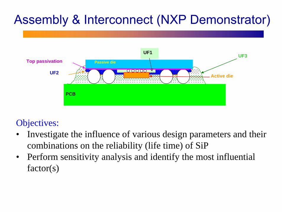
• Thrmo-mechanical modelling of Assembly and interconnect
• Stress and electromagnetic contamination monitoring within SiP packages
• Embedded Test
Lancaster University
• Centre for Microsystems Engineering– 4 academic staff, 5 RA’s, 4 PhD’s– Delivered against £3.4M in grant income over the past 10
years– Leads the European Design for Micro & Nano manufacture
community through the FP6 Network of Excellence (PATENT-DfMM)
Research, training and industrial services in the Engineering ScResearch, training and industrial services in the Engineering Science ience associated with Design for Manufacture Technology for Micro & associated with Design for Manufacture Technology for Micro & NanoNano
Technology based ProductsTechnology based Products
Key SkillsDesign methodology, modelling & simulation of MNT based structures and systems.Fault tolerant design, design for test, condition monitoring and test engineering for MNT based systems.Integration technology for MNT based systems (packaging)
Active ProjectsEU FP6 “INTEGRAMplus" Integrated MNT Platforms & Services (IP), “PATENT-DfMM” Design for Micro & Nano Manufacture (NoE) and “MINOS-EURONET”Micro-Nanosystems European Network pursuing the integration of NMS and ACC in ERA.EPSRC "Nanoelectronics”: from novelty toys to functional systems" 2006 – 2009 and IeMRC projects SiP-Design and I-Health.HEIF / NWDA Science & Entrepreneurship training award in MNT
Centre for Microsystems Engineering - Mission
University of Greenwich
• Centre for Numerical Modelling and Process Analysis– 5 Profs, 20+ Post Docs, 40 + PhD’s– One of largest groups in UK
• Electronics and Microsystems – 2 Profs, 3 Post Doc’s, 5 PhD’s– Over £2m of support since 1998 in electronics and microsystems
modelling.
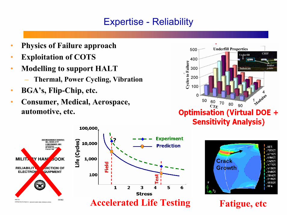
Expertise - Reliability
• Physics of Failure approach• Exploitation of COTS • Modelling to support HALT
Objectives:• Investigate the influence of various design parameters and their
combinations on the reliability (life time) of SiP• Perform sensitivity analysis and identify the most influential
factor(s)
Failure Models
• Solder (SAC)– Creep
• Failure Model (Fatigue)
)exp()(sinhRT
QA n
cr
−×=
•
ασγ
A n α Q/R
Sn37Pb 9.6E4 3.3 0.087 8058
Sn3.5Ag 9.0E5 5.5 0.065 8690
1)0014.0( −= WpN f
Creep Strain Energy
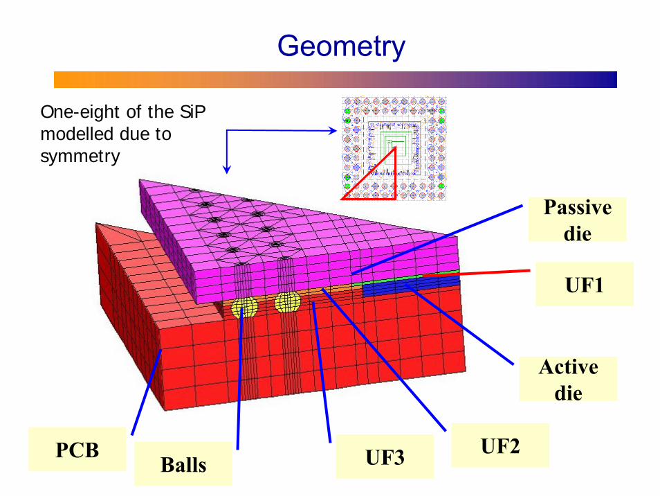
Geometry
PCBBalls
Passive die
Active die
UF1
UF2UF3
One-eight of the SiP modelled due to symmetry
Von Misses Stress and Deformation Modes for SiP 11× 11
Identifying Suitable Underfills
• Design Space– Youngs Modulus– CTE
• Design of ExperimentsE (GPa)
6
4
2
20 40 60 CTE (ppm/°C)
2040
60
2
4
6
0
50000
100000
150000
200000
250000
300000
350000
400000
450000
500000
Damage (Pa)
CTE(ppm/C)
E(GPa)
UF2
PCB
Passive die
Active die
UF3UF1Top passivation
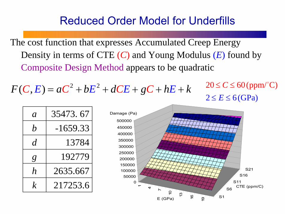
Reduced Order Model for Underfills
2 2( , )E ECF a b d E g hC C E kC= + + + + +
a 35473. 67b -1659.33d 13784g 192779h 2635.667k 217253.6
The cost function that expresses Accumulated Creep Energy Density in terms of CTE (C) and Young Modulus (E) found by Composite Design Method appears to be quadratic
1 4 7
10 13 16 19
S1
S6
S11
S16S21
050000
100000150000200000
250000
300000
350000
400000
450000
500000
Damage (Pa)
CTE (ppm/C)
E (GPa)
22 6(GPa)0 60(ppm/ C)C
E≤≤≤
≤ o
Identifying Critical Design Paramters
• What can designer change?– Underfill 2 & 3– Die Size– Die Thickness
UF2
PCB
Passive die
Active die
UF3UF1Top passivation
Actual values7×7; 9×9; 11×11mmNo; YesNo; Yes200µm; 400 µm
Die SizeReinforcement (UF2)Underfill (UF3)Passive Die Thickness
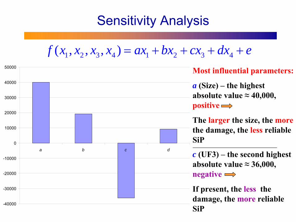
Sensitivity Analysis
1 2 3 4 1 2 3 4( , , , )f x x x x ax bx cx dx e= + + + +
• A contribution of a critical parameter to the cost function appears linear
Accumulated Creep Energy Density
Actual values Values in f7×7; 9×9; 11×11No; YesNo; Yes200µm; 400 µm
x1 Size -1; 0; 1x2 Reinforcement (UF2)
UF3Passive Die Thickness
-1; 1x3 -1; 1x4 -1; 1
Sensitivity Analysis
1 2 3 4 1 2 3 4( , , , )f x x x x ax bx cx dx e= + + + +The coefficients of the function have been determined by the Least Squares Method based on 18 experiments
-40000
-30000
-20000
-10000
0
10000
20000
30000
40000
50000
a b c d
Sensitivity Analysis
1 2 3 4 1 2 3 4( , , , )f x x x x ax bx cx dx e= + + + +Most influential parameters:
a (Size) – the highest absolute value ≈ 40,000, positive
The larger the size, the morethe damage, the less reliable SiP
-40000
-30000
-20000
-10000
0
10000
20000
30000
40000
50000
a b c dc (UF3) – the second highest absolute value ≈ 36,000, negative
If present, the less the damage, the more reliable SiP
Status
• The presence of UF3 can improve reliability of the SiPPackage
– CTE is the most influential– CTE as low as possible– Elastic Modulus as high as possible
• SiP design parameters– SiP size and presence of UF3 are the most influential parameters– Passive Die thickness and Presence of UF2 have smaller effect
on solder joint reliability– Recommendation: to improve reliability smaller package
size with suitable UF3 and thinner Passive Die
Inter Metallic Layer (IMC)
Solder Ball Reliability
Weibulldistribution
β : Weibull slope parameterη : Characteristic life parameterN : Random thermal life cycles to failureδ : IMC layer thickness
So ACK, Chan YC. Reliability studies of surface mount solder joints–effect of Cu-Sn intermetallic compounds. IEEE Trans Comp Pack Manuf Technol–Part B 1996; 19:661-668.
Objective : Build an Analytic Method of Reliability for Solder Joint in Package
Inter Metallic Layer growth
t : Reflow time
Dependence on reflow time (given temperature) :
δ : IMC layer thickness
T : Temperature of reflow
Dependence on temperature (given time) :
Reflow profile
* More accurate than polynomial fitting proposed in Huang W, Loman JM, Sener B. Study of the effect of reflow time and temperature on Cu-Snintermetallic compound layer reliability. Microelectronics reliability. 42(2002) 1229-1234.
Ts : saturated temperature
*
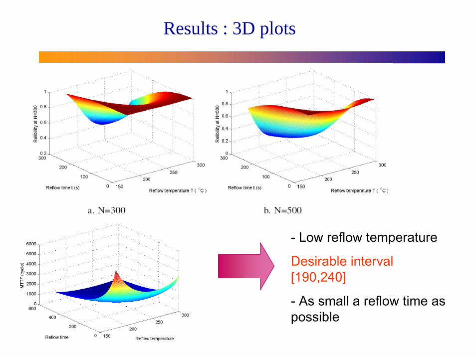
Results : 3D plots
- Low reflow temperature
Desirable interval [190,240]
- As small a reflow time as possible
• Reliability and MTTF of solder joint (63Sn37Pb) depend on reflow time and temperature.
• For high reliability we suggest reflow temperature between 190oC & 240oC. Avoid temperature between 250oC and 270oC . Reflow time is as low as possible.
• Next• Investigate the lower limit of the reflow time.• Extend this method to other solder material.
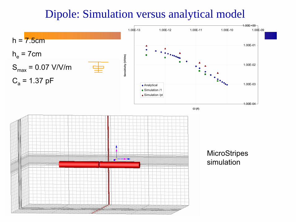
• Initiated work on standard EM probes• Initiated simulation work using MicroStripes• Working with Philips technology to design the EM
probes• Working with Philips to evaluate the shield
effectiveness using MicroStripes• Investigating Intra SiP coupling
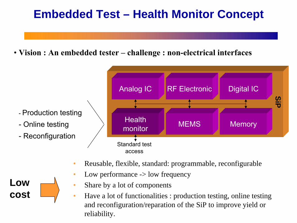
Digital ICRF Electronic
MEMS
Analog IC
MemoryHealthmonitor
Standard test access
SiP
- Production testing- Online testing- Reconfiguration
Embedded Test – Health Monitor Concept
• Reusable, flexible, standard: programmable, reconfigurable• Low performance -> low frequency• Share by a lot of components• Have a lot of functionalities : production testing, online testing
and reconfiguration/reparation of the SiP to improve yield or reliability.