3
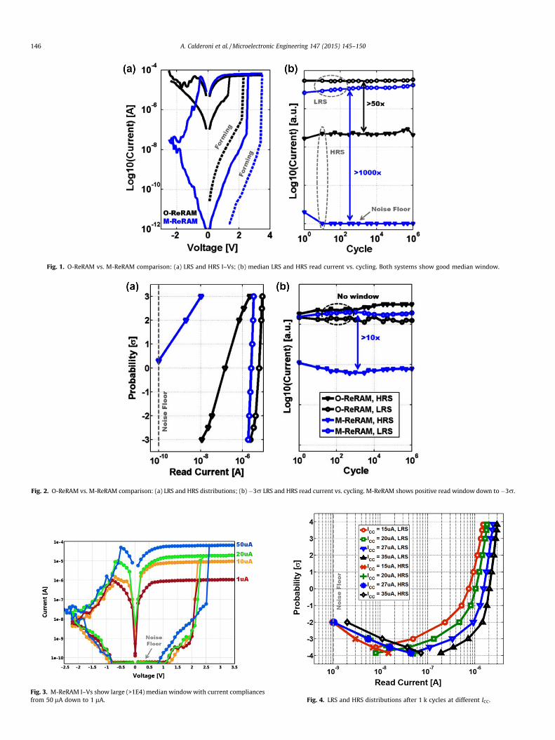
Engineering ReRAM for high-density applications Alessandro Calderoni ⇑ , Scott Sills, Chris Cardon, Emiliano Faraoni, Nirmal Ramaswamy Micron Technology Inc., Boise, ID, USA article info Article history: Received 23 February 2015 Received in revised form 6 April 2015 Accepted 7 April 2015 Available online 11 April 2015 Keywords: Resistive memory Endurance Noise Variability MLC Cross-point abstract Resistive random access memory (ReRAM) devices are emerging candidates for the next generation of nonvolatile high-density memory (Sills et al., 2014). The value proposition for this technology is bit alter- ability, high speed operation, long retention and high endurance. In addition, low-power and low-current operation is highly desirable for high-density memory systems targeting the growing mobile market. This paper presents various challenges in engineering a ReRAM cell suitable for high-density applications such as material selection, programming algorithms, noise issues and scaling path. Ó 2015 Elsevier B.V. All rights reserved. 1. Material selection: O-ReRAM or M-ReRAM? The spectrum of materials showing non-volatile resistance switching is wide and includes several metal oxides as well as chalcogenide-based systems [2,3]. Filamentary switching between a high-resistance state (HRS) and a low-resistance state (LRS) is obtained by oxygen or metal ion movement (O-ReRAM and M-ReRAM, respectively). The reference O-ReRAM stack presented here comprises: a TiN bottom electrode (BE), an amorphous ALD HfSiOx dielectric layer and a reactive Ti top electrode; whereas the M-ReRAM stack is made by a TiN BE, an electrolyte layer and a copper ion reservoir. The BE size is 30 nm. Stable median endurance characteristics are possible for both systems up to 1E6 cycles with read window (LRS to HRS ratio) >50 and >1000 for O-ReRAM and M-ReRAM, respectively (Fig. 1). High-density applications require high read window for a large number of bits, which means that a fair assessment of different ReRAM systems can only be done by comparing variability and full distributions [4]. Read, program and cell-to-cell variability have to be carefully evaluated on the same test vehicle to compare the per- formance of different systems. Fig. 2a shows read distributions for the two reference systems: although the median window is wide for both systems, variability makes the read margin (difference between LRS and HRS currents at 3r) much worse for O-ReRAM compared to M-ReRAM. The choice of a system with a large median window between LRS and HRS, as well as a low variability, is thus indispensable for reliable operations through cycling (Fig. 2b). For this reason, M-ReRAM has been selected over O-ReRAM as a reference material for high-density applications. 2. Low current operation High-density memory would require low current operation because maintaining high drive capability in scaled access devices is a significant challenge. To realize the advantages of low voltage operation, programming currents need to be low (since parasitic drops across routing and drivers will be high if the programming current is high). It’s thus necessary to engineer a cell capable of operating well below 50 lA. Fig. 3 shows M-ReRAM I–Vs for a wide range of current compliance, from 50 lA down to 1 lA. The cell functions well down to currents as low as 1 lA with a large median read window (>1E4). Nevertheless this intrinsic capability is not enough to ensure reliable operation at low current. This is due to the fact that all the variability components such as read and program noise, increase at low current compliance (I CC ) [4]. As I CC is decreased, the number of metal cations comprising the filament significantly reduces, leading to increased variability. Fig. 4 shows that the read margin narrows at very low compli- ances (<30 lA), although the median read window is >1E4. The lower number of atoms in the conductive filament at low http://dx.doi.org/10.1016/j.mee.2015.04.044 0167-9317/Ó 2015 Elsevier B.V. All rights reserved. ⇑ Corresponding author. E-mail address: [email protected] (A. Calderoni). Microelectronic Engineering 147 (2015) 145–150 Contents lists available at ScienceDirect Microelectronic Engineering journal homepage: www.elsevier.com/locate/mee