November 2016 Guiding Embedded Designers on Systems and Technologies ARM® Cortex®-R52 Advances Autonomous Safety Embedded FPGAs Add Flexibility ARM for GPGPU www.eecatalog.com/arm Sponsors Engineers’ Guide to ARM Technology
Transcript
November 2016
Guiding Embedded Designers on Systems and Technologies
ARM® Cortex®-R52 Advances Autonomous Safety
Embedded FPGAs Add
Flexibility
ARM for GPGPU
www.eecatalog.com/armSponsors
Engineers’ Guide to ARM Technology
3
CONTENTS
IN THIS ISSUE
Embedded Systems Engineering is published by Extension
Media LLC, 1786 18th Street, San Francisco, CA 94107.
ARM Cortex-R52: Meeting the Challenge of Autonomous SystemsBy Caroline Hayes, Senior Editor 5
Picturing ARM for GPGPU Applications Q&A with Doug Patterson, Aitech Defense Systems By Anne Fisher, Managing Editor 10
Microcontroller Architects Look to Embedded FPGAs for Flexibility Tony Kozaczuk, Flex Logix 12
Bluetooth 5 Could Unleash the Audio Accessory MarketBy Caroline Hayes 15
Product Showcases
Development Tools
Development Tools
Aldec Inc
TySOM High Performance
Embedded Development 17
Embedded Software
Operating Systems (OS/RTOS)
WITTENSTEIN high integrity systems
SAFERTOS® 18
IoT
IoT
EMAC, Inc.
SoM-iMX6M 19Technologic Systems
TS-7680 Single Board Computer 20
November 20165
engineers guide to ARM Technologyengineers guide to ARM Technology
ARM Cortex-R52: Meeting the Challenge of Autonomous SystemsThe new ARM® Cortex®-R52 can meet raised functional safety standards across multiple markets, from automotive to industrial and including healthcare. ARM Product Manager, James Scobie, tells Caroline Hayes how the company’s latest processor can meet raised standards in increasingly complex systems.
Across multiple markets, automation is increasing complexity
in electronic systems, fuelling demand for functionally safe
operation. In vehicles, there are already driver assistance systems,
with functionality on the way to autonomy, such as automatic lane
changing. Engine management systems are also increasingly complex
to meet stringent emission controls. They must also control the engine
to prevent damage or hazards, and, as electrification progresses, sys-
tems must control powerful motors and manage large Lithium-ion
batteries, which contain significant amounts of energy.
The autonomous trend is also being seen in other areas. Conventional
robotic production lines, where robots carry out a defined fixed task
and are segregated from operators, are being replaced by collaborative
industrial robots. These have unconstrained interaction with human
operators, sensing their environment and taking action safely. They
may be capable of selecting and placing the correct component while
working in conjunction with a human operator. They are also being
used in environments that are too harsh for humans, such as the
nuclear industry.
Surgical robots are increasingly being used in operating theaters with
remote surgery, and to deliver medication. In future, commercial
autonomous drones are expected to need these characteristics.
As a result of these levels of automation, systems require
functional safety at a higher level than previous genera-
tions of systems demanded. The new ARM® Cortex®-R52
processor has been introduced to addresses the chal-
lenging needs of these types of systems.
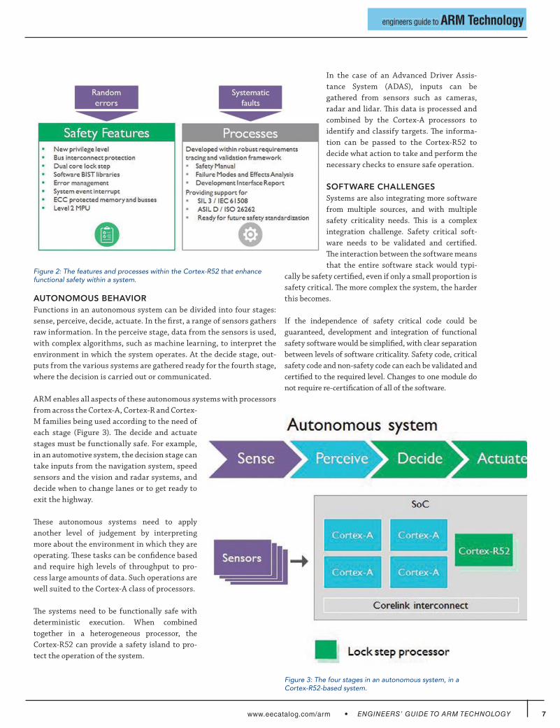
THE AUTOMOTIVE CASEA functionally safe system has to be protected against
two types of errors: random or systematic (Figure 1).
The impact of random errors, for example a memory
bit flipping due to radiation, can be protected against
through the inclusion of features in the processor.
Cortex-R52 integrates the highest level of safety features
of any ARM processor to guard against this type of error.
Systematic errors are typically the result of software
or design errors. Protection against these is provided
by appropriate processes and procedures at the design
stage. Cortex-R52 has been developed from the ground
up and a comprehensive safety documentation package
simplifies and reduces the effort needed by SoC part-
ners in certifying the end system.
There are a number of different standards and guidelines
related to functional safety, such as ISO 26262. (For
more information about functional safety, there is The
Functional Safety Imperative in Automotive Design
white paper.)
There are many, different applications where functional
safety and fast, deterministic execution is necessary. In
many real-time control systems, the application can be
managed either with a single Cortex-R52 processor or
across multiple homogeneous processors. This might be
typical in a conventional control system, like an automo-
tive engine management system or industrial controller.
Figure 1: In a vehicle braking system, safety features in the processor protect against random errors and system faults.
By Caroline Hayes, Senior Editor
7
engineers guide to ARM Technologyengineers guide to ARM Technology
www.eecatalog.com/arm
AUTONOMOUS BEHAVIOR Functions in an autonomous system can be divided into four stages:
sense, perceive, decide, actuate. In the first, a range of sensors gathers
raw information. In the perceive stage, data from the sensors is used,
with complex algorithms, such as machine learning, to interpret the
environment in which the system operates. At the decide stage, out-
puts from the various systems are gathered ready for the fourth stage,
where the decision is carried out or communicated.
ARM enables all aspects of these autonomous systems with processors
from across the Cortex-A, Cortex-R and Cortex-
M families being used according to the need of
each stage (Figure 3). The decide and actuate
stages must be functionally safe. For example,
in an automotive system, the decision stage can
take inputs from the navigation system, speed
sensors and the vision and radar systems, and
decide when to change lanes or to get ready to
exit the highway.
These autonomous systems need to apply
another level of judgement by interpreting
more about the environment in which they are
operating. These tasks can be confidence based
and require high levels of throughput to pro-
cess large amounts of data. Such operations are
well suited to the Cortex-A class of processors.
The systems need to be functionally safe with
deterministic execution. When combined
together in a heterogeneous processor, the
Cortex-R52 can provide a safety island to pro-
tect the operation of the system.
In the case of an Advanced Driver Assis-
tance System (ADAS), inputs can be
gathered from sensors such as cameras,
radar and lidar. This data is processed and
combined by the Cortex-A processors to
identify and classify targets. The informa-
tion can be passed to the Cortex-R52 to
decide what action to take and perform the
necessary checks to ensure safe operation.
SOFTWARE CHALLENGESSystems are also integrating more software
from multiple sources, and with multiple
safety criticality needs. This is a complex
integration challenge. Safety critical soft-
ware needs to be validated and certified.
The interaction between the software means
that the entire software stack would typi-
cally be safety certified, even if only a small proportion is
safety critical. The more complex the system, the harder
this becomes.
If the independence of safety critical code could be
guaranteed, development and integration of functional
safety software would be simplified, with clear separation
between levels of software criticality. Safety code, critical
safety code and non-safety code can each be validated and
certified to the required level. Changes to one module do
not require re-certification of all of the software.
Figure 2: The features and processes within the Cortex-R52 that enhance functional safety within a system.
Figure 3: The four stages in an autonomous system, in a Cortex-R52-based system.
November 20169
engineers guide to ARM Technologyengineers guide to ARM Technology
ARMV8-R ARCHITECTUREFor many of these systems, this separation must be
achieved whilst still maintaining deterministic execution.
Cortex-R52 provides the hardware to support both iso-
lation and real-time execution, through the addition of
a new exception level and two-stage MPU, introduced
in the ARMv8-R architecture. Monitor or hypervisor
software can manage access to resources and create
sandboxes to protect each task. The design of the
Cortex-R52 allows for fast switching between protected
applications and maintains deterministic execution.
As well as protecting software, it simplifies the integra-
tion of code into a single processor. Using a hypervisor,
multiple operating systems can be supported to con-
solidate applications.
Many systems require deterministic operation, with
the appropriate action being controlled, and also per-
formed at the right time, without significant delay,
regardless of what else is happening in the system.
The Cortex-R family offers real-time processors and
Cortex-R52 is the first processor in the ARMv8-R
architecture and further extends the capabilities of
the Cortex-R5, both in terms of functional safety and
increased performance.
Cortex-R52 delivers up to 35% higher single core per-
This performance increase is enhanced by additional real time perfor-
mance gains. Interrupt latency has been reduced to half that of the
Cortex-R5 with fast access and integration of the interrupt controller
within the cluster. The improved Memory Protection Unit, with finer
granularity and faster reconfiguration, significantly reduces context
switching time, to 14 times faster than the Cortex-R5. System perfor-
mance is also increased as twice as many Cortex-R52s than Cortex-R5s
can be integrated within a cluster.
Cortex-R52 supports an adaptable memory architecture with inte-
grated deterministic Tightly Coupled Memories. These enable assured
memory latencies and can be allocated to instruction or data and con-
figured in a range of sizes. The processor supports a rich set of interface
ports around which the system can be built, for example a low latency
peripheral port, AXI interfaces and a dedicated wide Flash memory
interface to provide access to resources with managed arbitration.
ECOSYSTEM SUPPORT Ecosystem partners provide software packages, drivers, stacks, oper-
ating systems and tools to simplifying development. Adopters can
leverage the common architecture to reduce costs as multiple suppliers
address requirements. They can also can develop on a single platform
and implement heterogeneous systems and port solutions between
different platforms faster and with more reliable results. For more
information visit software development tools for ARM Cortex-R.
One ecosystem partner is Synopsys, which has announced tool sup-
port for the Cortex-R52.
For an extended version of this piece, please visit the ARM Connected
Community.
10
engineers guide to ARM Technologyengineers guide to ARM Technology
www.eecatalog.com/arm
Picturing ARM for GPGPU Applications Q&A with Doug Patterson, Aitech Defense SystemsThe factors that go into balancing performance and cost-effectiveness for GPGPU-based systems
Editor’s note: Just prior to Aitech Defense Solutions announcing the avail-
ability of its fanless rugged GPGPU supercomputer, Doug Patterson, the
company’s VP, Military & Aerospace Business Sector, responded to a few
questions about GPGPU-based systems.
EECatalog: What are some of the arguments for and against the
choice of ARM for the Tegra GPGPU?
Doug Patterson, Aitech:
FORThis choice was made by NVIDIA engineers,
and it’s a smart one. For the past several years,
we’ve seen a real boost in the ARM architec-
ture performance, while still keeping power
consumption low. The big players like Hewlett
Packard (HP) are already selling servers with
ARM (look for “Moonshot” server), a very strong
sign that ARM successfully penetrated not only
the mobile market (in this market ARM is no doubt a leader), but also
enterprise servers.
HP has become the first major vendor to add a 64-bit
ARM server to its server product line price list, but it
will not be the last. Dell has built 64-bit ARM-based
servers for particular customers, but HP is the first
big vendor that’s selling one as a standard product.
ARM architecture has always been a good choice for
embedded systems. The main selling points—low
power consumption with a superb level of compute
power in a small physical space—make ARM good for
building SWaP-optimized embedded systems.
The Linux OS and app developer’s community running the
well-known and widely used “Ubuntu” Linux distribution
supports ARM very well. So, if your target is building high-
performance embedded systems, key advantages that play
nicely into NVIDIA’s strengths, ARM is definitely a good
choice. Aitech’s rugged A176 Cyclone GPGPU, using the
NVIDIA Tegra TX1, brings 1 TFLOP, or >60 GFLOPS/Watt
of performance, into ~20 cu-in.
AGAINSTComparing ARM to x86 architecture, there are some
caveats with the development and integration process.
ARM architecture doesn’t support Windows OS, which
makes the target market for ARM Linux-oriented only.
It therefore requires special knowledge during the
development and integration stage, since hardware is
not always available for native platform development
during the first stage of development.
This means that a cross compiler is needed for software
development. Although these differences exist, they
are easily overcome by training, so the learning curve is
pretty flat and relatively fast.
EECatalog: What trends and developments in advanced
sensor processing have you been keeping an eye on?Figure 1: Patterson explained why he believes that other major vendors will follow HP in looking to ARM architecture.
By Anne Fisher, Managing Editor
Doug Patterson, Aitech
November 201611
engineers guide to ARM Technologyengineers guide to ARM Technology
Patterson, Aitech: Sensors are becoming even more
intelligent. With embedded processing platforms
becoming smaller, lighter and lower power, and with
orders of magnitude more performance, it’s easier to
push much more of the sensor pre-processing out to
the sensor. Tasks include pre-filtering/noise rejection
or video motion/edge-detection to the most advanced
automatic target recognition. This has long been the
generally accepted definition of distributed processing,
and now it’s here, with 1 TFLOP in small form factors
making it a reality.
EECatalog: What are the persistent problems defense
applications face when trying to first, select the correct
GPGPU for their challenges, and second, deploy the
GPU effectively?
Patterson, Aitech: The main problems from experi-
ence include issues related to heat/power dissipation
and challenges of the app development process, with
regard to actual versus expected performance.
Performance always comes at the price of higher power
consumption, unless you are moving to the more special-
ized architectures that provide more performance and
less power consumption compared with previous models.
Since performance is the primary “key” requirement for
GPGPU systems, the customer usually compromises and
picks the “as fast as possible” GPGPU, performs a soft-
ware evaluation and then starts to search for a “rugged”
solution. Among the factors to consider are:
What is the form factor needed?
How small and how high is the power density?
How is the unit is to be cooled?
It’s up to the hardware/system supplier (Aitech, for
example) to understand all the system architecture
aspects and propose the proper, most cost-effective
solution without jeopardizing GPGPU performance.
Only a company designing and building not only the
electronics, but also developing rugged enclosures and
building rugged systems is equipped to deal with these
(and related) challenges.
EECatalog: How nervous are companies trying to keep up with mil-
aero advanced sensor processing demands that the solution they
select will be out of date too quickly?
Patterson, Aitech: The demand for more and more processing power
from GPGPU is constantly growing. We see it from our customers: Each
new project starts with the question: “Can you do it faster?” Not only
is actual performance important, but you also need to have enough
“provisioned power” for the next deployment without changing the
hardware.
Companies thinking about the longer term, like Aitech, provide a very
modular solution. So even when the customer is utilizing and investing
the time with a certain GPGPU, we can easily swap and move to the
next generation GPGPU device, and in most cases, maintain backward
software compatibility for the new one. The customer can again be on
the “safe side” with the best performance he can get. We even have a
program, COTSLifecycle+, dedicated to providing our customers with
a minimum of 12 years of same-product continuity.
So, are they nervous about GPGPU technology? Probably not, maybe
more concerned. Once the evaluation is done, and they see that they
have enough “GPGPU power,” they seem to be fine.
EECatalog: Closing thoughts?
Patterson, Aitech: The Tegra TX1 is a generation ahead in perfor-
mance and requires less than half the power dissipation of products
using older NVIDIA Maxwell technology.
Aitech is working closely with NVIDIA in the GPGPU applications
field, and at NVIDIA’s request presented at GTC Europe Sept. 28-29
in Amsterdam. We’re constantly benchmarking and choosing the
best available performance with the lowest power consumption in
the smallest form factor. Today, Aitech is deploying GPGPU solutions
not only at the board level (C874+C530), but also on a fully integrated
system level (A191, A195, A196).
Since we are the “design house,” we’re doing the electronics as well
as the mechanics, system integration, qualification, and software
development, etc. This combination makes us an ideal supplier of
GPGPU-based systems. Seeing that the ARM and NVIDIA architec-
tures are getting a performance boost each year, we’re already actively
designing two successor products and building a new product line
based on NVIDIA Jetson TX1, which has an ARM quad CPU teamed
with the NVIDIA CUDA GPU in the same device package.
12
engineers guide to ARM Technologyengineers guide to ARM Technology
www.eecatalog.com/arm
Microcontroller Architects Look to Embedded FPGAs for FlexibilityWhy embedded FPGAs are set to enhance and complement ARM processors
Today, microcontroller families typically have dozens
of versions that have various combinations of GPIO
configurations: SPIs, UARTs, I2Cs, etc. to address
the needs of different customers. This requires mask
changes for each version. A new version takes quarters
to go through the design and verification process. Now
that microcontrollers are moving to the 40nm node
where mask costs are ~$1M, a new solution is required.
Embedded FPGAs provide this solution by enabling
microcontrollers to have a part or all of their GPIO
subsystem be programmable and reconfigurable. This
enables any GPIO to be any serial pro-
tocol and enables some processing to be
done in the embedded FPGA, speeding
response offloading the embedded pro-
cessor, and perhaps saving energy.
Flex Logix provides EFLX embedded FPGA
in the 40nm node, which will be integrated
into the I/O subsystems of future micro-
controllers to provide this flexibility and
reconfigurability (Figure 1). Embedded FPGA can also connect to higher
performance buses such as AHB and AXI.
WHAT IS AN EMBEDDED FPGA? An FPGA combines an array of programmable/reconfigurable logic
blocks in a programmable interconnect fabric. In an FPGA chip, the
outer rim of the chip consists of a combination of GPIO, SERDES and
specialized PHYs such as DDR3/4. In advanced FPGAs, the I/O ring
is roughly 1/4 of the chip and the “fabric” is roughly 3/4 of the chip.
The “fabric” itself is mostly interconnect in today’s FPGA chips, where
20-25% of the fabric area is programmable logic and 75-80% is pro-
grammable interconnect.
An embedded FPGA is an FPGA fabric without the surrounding ring of
GPIO, SERDES, and PHYs (Figure 2). Instead, an embedded FPGA con-
nects to the rest of the chip using standard digital signaling, enabling
very wide, very fast on-chip interconnects.
To achieve high density, Flex Logix provides embedded FPGA as hard
IP proven in silicon. Microcontrollers now are moving to 40nm, where
Flex Logix provides an EFLX-100 IP core in TSMC 40ULP/LP, which is
by itself a stand-alone embedded FPGA, with 120 LUTs, reconfigurable
interconnect, 152 inputs and 152 outputs. Each EFLX LUT is actually
By Tony Kozaczuk, Flex Logix
Figure 2: Standard digital signaling connects an embedded FPGA to the rest of the chip.
Figure 1: 40nm node EFLX embedded FPGA depicted as part of a microcontroller I/O subsystem.
November 201613
engineers guide to ARM Technologyengineers guide to ARM Technology
a dual-4-input LUT, each with its own output Flip Flop that can be
combined to make a single 5-input LUT.
For larger arrays, the EFLX-100 can be “tiled” to build arrays up to 5x5 or
3,000 LUTs of reconfigurable logic with 760 inputs and 760 outputs. The
EFLX-100 has two versions that can be mixed together in arrays. One
version is all logic and the other has two 22-bit MACs for DSP functions.
EFLX arrays can be integrated into an SoC or MCU in three common
ways as depicted in Figure 3.
The embedded FPGA is programmed using Verilog and VDHL, which
are input to a synthesis tool such as the Synopsys Synplify tool. Then
the EFLX Compiler packs/places/routes the array and generates a
bit stream which programs the EFLX array to emulate the RTL. The
bit stream for a single EFLX-100 is ~50K bits and it can be stored in
the same flash memory that stores the embedded processor code.
The EFLX array can be reprogrammed at any time, just like with an
embedded processor.
CONNECTION TO THE APB BUSAn APB bus requires 102 connections: 32 address, 32
data in, 32 data out, clock, 5 controls.
An EFLX-100 has 152 inputs and 152 outputs, so even a
small embedded FPGA can directly connect to the APB
bus. There are 83 inputs and 119 outputs available even
for a single EFLX-100 after connecting to the APB bus.
The EFLX can interface directly to the APB bus without
any additional logic except for the PREADY signal, which
needs to be isolated when the EFLX is power gated. An
EFLX-100 has 120 LUTs, and only seven are required to
implement the logic needed to implement an APB slave interface. Of
course, the logic for the Slave Interface can also be hardwired external
to the embedded FPGA, which frees up a little more room for recon-
figurable logic. The EFLX array only supports unidirectional I/Os (i.e.
inputs and outputs only) and all the I/Os are general purpose CMOS
I/Os. When the EFLX interfaces to the I/O pins of the MCU/SoC, an
external buffer is required between the EFLX array and the I/O pad
(Figure 4). The I/O buffer can be a unidirectional buffer or a bidirec-
tional buffer. If it is a bidirectional buffer, the EFLX array needs to
control the direction of that buffer used by the array.
GPIO AND SERIAL PERIPHERALSThe EFLX array can be used to perform I/O functions in an MCU/SoC.
There are numerous serial protocol peripheral standards, and every
customer wants a different combination. Common versions are UART,
SPI and I2C. Microcontroller companies typically design and stock
slightly different versions with a couple of each or, in some cases, up to
five or six of each. However, nobody needs all of them, and some cus-
tomers want other serial I/O peripherals. With an embedded FPGA,
it is possible to implement exactly the serial I/O peripheral needed in
the EFLX fabric.
For example, an EFLX array can be configured
either as an APB 32-bit GPIO port or an APB
simple UART (Figure 5). When reconfigured as a
32-bit GPIO port, the function only uses 93 LUTs
(seven LUTs for the APB interface and 86 LUTs
for the GPIO registers) and can run @ 50MHz on
an eHVT/SVT EFLX array (V=0.85v, 125°C, slow/
slow process corner). When the array is reconfig-
ured as a simple UART master (no flow control or
FIFOs), the function uses 75 LUTs and can run @
36MHz (UART data rate) on an eHVT/SVT EFLX
array (V=0.85v, 125°C, slow/slow process corner).
In the two above examples, the EFLX array uses
the same I/O buffers, which are repurposed for
the specific function configured in the array.
If the goal is to use 32 GPIOs with 24-GPIO ports
and up to 4 UARTs, then 93 + 4*75 =393 LUTs are
required. A 2x2 EFLX-100 array has 480 LUTs
and can fit the functionality of the desired I/Os. In addition, a 2x2
EFLX-100 array can fit a full function UART such as a 16550, which
Figure 3: Three ways to integrate EFLX arrays into an SoC or MCU.
Figure 4: Showing requirement for an external buffer between the EFLX array and the I/O pad in a situation where the EFLX interfaces to the I/O pins of the MCU/SoC .
14
engineers guide to ARM Technologyengineers guide to ARM Technology
www.eecatalog.com/arm
requires 365 LUTs without any optimizations of the design for a
reconfigurable fabric.
Other serial peripherals can be similarly implemented in EFLX, and
there are a wide range of types. Many suppliers of the RTL for any
kind of serial peripheral provide IP solutions for FPGA chips. These
can be used in embedded FPGA as well, since EFLX is programmed
using Verilog or VHDL.
Another option, which would reduce silicon area, would be to imple-
ment the minimum desired serial peripherals in hard-wired RTL,
routing their signals through the EFLX to any of the GPIO, then
adding additional serial peripherals in the EFLX array. Figure 6 shows
the EFLX array functioning as an I/O switch as well as adding addi-
tional I/O functionality.
PROCESSING TO SAVE ENERGY AND IMPROVE RESPONSIVENESSRTL to process inputs and outputs can be added to the EFLX embedded
FPGA. For example, a 16-bit 5-tap FIR filter can be implemented using
Figure 5: It’s possible to deploy exactly the serial I/O peripheral required.
Figure 6: An I/O switch with additional I/O functionality.
Figure 7: Implementing a 16-bit 5-tap FIR filter.
the MACs in the DSP version
of the EFLX-100. This RTL will
fit in 3 EFLX-100 tiles using 5
MACs with no additional logic
LUTs (Figure 7).
This RTL code will execute a
16-bit 5-tap FIR filter in less
time than an ARM processor
and more importantly using
less energy. In TSMC40ULP
eHVT, this function requires
only 10.75nJ, which is 5x less
than an ARM processor core
not even counting the memory
access energy of an ARM pro-
cessor. As a result, an EFLX
array can extend battery life for simpler, repetitive processing of I/O
and only wake up the ARM processor to handle more complex tasks
as required.
Many other kinds of I/O processing are possible and these are limited
only by the size of the EFLX array chosen. An RTL state machine in the
EFLX array can identify and respond to critical input patterns much
more quickly than the more distant ARM processor.
Embedded FPGA provides a new way for microcontroller architects
to deliver a wide range of serial and other I/O functionality using a
single mask set. It even provides end customers the potential to pro-
gram the array to offload processing tasks into the embedded FPGA
from the ARM processor to save energy and improve responsiveness.
Embedded FPGA certainly won’t displace ARM processors, but it will
instead enhance and complement them.
Tony Kozaczuk is Director, Solutions Architecture, Flex Logix Technologies, Inc.
November 201615
engineers guide to ARM Technologyengineers guide to ARM Technology
Bluetooth 5 Could Unleash the Audio Accessory MarketSince Apple announced that it is removing the headphone jack from the iPhone 7 and iPhone 7 Plus, launched earlier this month, many industry watchers have expressed concern, but there are plenty of precedents for similar industry disruption, argues Paul Williamson, general manager of the wireless business unit at ARM®. Here’s what the new Bluetooth low energy standard could mean for consumers and the evolution of design.
Caroline Hayes: What is included in the Bluetooth 5 standard?
Paul Williamson: The latest Bluetooth® low energy (Bluetooth 5)
standard introduces an increased data rate of 2-Mbit per sec. This data
rate could allow enhanced quality audio experiences to be delivered
with the same ultra low-power envelope that Bluetooth low energy
introduced.
Caroline Hayes: How has the introduction of wireless technology
changed consumer expectations?
Paul Williamson: In 2012 Apple introduced the lightning connector
ending almost a decade of the 30-pin connector, and an entire line
of audio accessories became obsolete over the coming year. Jawbone
captured this moment and rode the market disruption to deliver con-
sumers a new product and experience in audio, the Jambox wireless
Bluetooth speaker.
Caroline Hayes: A phone without a headphone jack is
unthinkable—how does Bluetooth 5 make it palatable?
Paul Williamson: The demise of the headphone jack,
possibly as a result of the introduction of the iPhone
7/iPhone 7 Plus, could herald opportunities for the
industry. In the short term it is clear that user adoption
of wireless headphones will rise. A range of existing
Bluetooth products are ready to serve this initial
demand, but just as the Jambox fired the starting gun
on innovation in wireless speaker design, we can expect
similar innovations in wireless headphones.
The announcement may kick-start the industry to
deliver smaller, in-ear wearables that can provide the
ability to have truly wireless audio. In a few years,
we are less likely to be talking about the form of the
product, and more likely to be looking at the function-
ality. As the recently announced collaboration between
Bragi and IBM shows,
the future of the earbud
is likely to be about new
user experiences. By com-
bining Bragi’s The Dash
smart earphones with
IBM’s Watson IoT plat-
form, the collaboration
hopes to deliver hearable
technologies, using Wat-
son’s language translation
and speech-to-text capa-
bilities for users to receive
instructions and interact
with colleagues, as well
as to track location and
environments of workers.
Figure 1: Support is already in place for Bluetooth 5, with IP and RF-to-stack solutions.
By Caroline Hayes, Senior Editor
16
engineers guide to ARM Technologyengineers guide to ARM Technology
www.eecatalog.com/arm
Similar to the film Her, where a writer develops a relationship with a
personal assistant OS, the in-ear personal assistant may be the next
development that begins with the removal of a decades-old, physical
connector.
Caroline Hayes: Is this science-fiction from the film world, or is it
soon to be reality?
Paul Williamson: Truly wireless earbuds are likely to hit the main-
stream. Following innovations by Bragi with The Dash, wireless stereo
earbuds are becoming more popular with consumers. Long-standing
brands, such as Samsung and Jabra, have introduced their own take
on the format.
Caroline Hayes: Can developers begin implementing Bluetooth 5
straight away?
Paul Williamson: As with most battery-powered accessories, we
should expect to see smaller, energy-efficient form factors appear in
the hearing aid and headphone markets in the future. The Bluetooth
5 enhancements could help to achieve even longer active use and
standby time for the user, enabling devices to be worn with constant
connection to a smartphone, for listening to music/
audio, or collecting a range of sensor data, such as heart
rate measurements.
To be able to deliver longer listening time and smaller
products, semiconductor companies will need to
respond with greater integration in the SoC. ARM®
offers RF-to-stack solutions, all in-house. It is ready to
support semiconductor partners with drop-in, silicon-
proven, Bluetooth low energy IP with ARM’s sub-1 Volt
Cordio radio IP.
The ARM® Cordio® IP can support the enhancements to
the Bluetooth standard, as demonstrated at Bluetooth
World 2016 and DAC 2016.
This is a key component in delivering further highly
integrated, in-ear, Bluetooth low energy wireless ear
bud design, and is ideally combined with the μA/MHz
power and area optimized Cortex® -M4 processor.
Caroline Hayes has been a journalist, covering the elec-
tronics sector for over 20 years. She has worked on many
titles, most recently the pan-European magazine, EPN.
ARM Technologies ONLINE
Explore...➔ Top Stories and News
➔ White Papers
➔ Expert Opinions (Blogs)
➔ Exclusive Videos
➔ Valuable Articles
Sign up for the ARM Technologies Quarterly Report email newsletter
www.eecatalog.com/arm
www.eecatalog.com/arm
November 201617
CONTACT INFORMATION
engineers guide to ARM Technologyengineers guide to ARM Technology
Aldec Inc
TECHNICAL SPECS
◆ Programmable FPGA Fabric
◆ Onboard DDR3 Memory
◆ Various Peripherals and Interfaces
◆ Small Form Factor
◆ Reference Embedded Linux Designs
APPLICATION AREAS
Industrial IoT, Automotive, Robotics, UAV
AVAILABILITY
Aldec is now shipping the Xilinx® Zynq®-based TySOM Embedded Development Kit in two configurations.
TySOM High Performance Embedded Development
Compatible Architectures: Xilinx Zynq SoC FPGA with Dual-Core ARM Cortex-A9
Compatible Linux and Android OS: Linux
The TySOM™ Embedded Development Kit is for the embedded
designer who needs a high-performance RTL simulator/debugger
for their embedded applications such as IoT, Factory Automation,
UAV and Automotive. The kit includes Riviera-PRO™ Advanced
Verification Platform and a Xilinx® Zynq™ development board
that contains single Zynq chip (FPGA + Dual ARM® Cortex-A9),
memories (DDR3, uSD), communication interfaces (miniPCIe,
Ethernet, USB, Pmod, JTAG) and multimedia interfaces (HDMI,
audio, CMOS camera).
FEATURES & BENEFITS
◆ Zynq Development Board containing programmable FPGA and dual ARM® Cortex-A9 cores for embedded designers developing complex systems with custom RTL and embedded applications. The board includes memories (DDR3, uSD), communication interfaces (miniPCIe, Ethernet, USB, Pmod, JTAG) multimedia interfaces (HDMI, audio, CMOS camera) and daughter board expansions via FMC.
◆ Advanced RTL Debugging features include Dataflow, Post-Simulation Debug, Advanced Waveform Viewer, Plot/Image Viewer, Xtrace and Code Coverage.
◆ Supports Xilinx® Vivado™ and SDK™ development flow. Zynq-based hardware designs are created in Vivado and simulated in Riviera-PRO as the target simulator in Vivado. Software applications created in SDK are executed on the TySOM board as bare-metal or Linux-based applications. Riviera-PRO and Vivado cooperation is powerd by the Xilinx TCL Store Aldec Integration App.
◆ Pre-Validated Ubuntu Embedded Host Reference Design where users are able to turn the TySOM board into a full-stacked Linux box, compile and run complex Linux applications and learn the basics of the main Linux concepts and frameworks. The reference design contains the hard-ware (Vivado design) and software (Linux setup) support for the next groups of peripherals used with the TySOM board
◆ Target applications include Industrial IoT, Factory Automation, UAV, Automotive, Robotics and Computer Vision
Aldec Inc2260 Corporate Circle Suite 400Henderson, NEVADA 89074United StatesTel: (702) [email protected]
Deve
lopm
ent To
ols D
eve
lopm
ent
Tools
THE DESIGN VERIFICATION COMPANYR
18www.eecatalog.com/arm
CONTACT INFORMATION
engineers guide to ARM Technologyengineers guide to ARM Technology
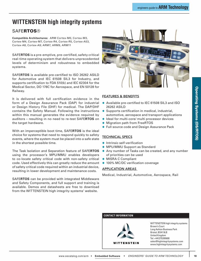
WITTENSTEIN high integrity systems
FEATURES & BENEFITS
◆ Available pre-certified to IEC 61508 SIL3 and ISO 26262 ASILD
◆ Supports certification in medical, industrial, automotive, aerospace and transport applications
◆ Ideal for multi-core/ multi processor devices◆ Migration path from FreeRTOS◆ Full source code and Design Assurance Pack
TECHNICAL SPECS
◆ Intrinsic self-verification◆ MPU/MMU Support as Standard◆ Any number of Tasks can be created, and any number
of priorities can be used◆ MISRA C Compliant◆ 100% MC/DC verification coverage
APPLICATION AREAS
Medical, Industrial, Automotive, Aerospace, Rail
SAFERTOS®
Compatible Architectures: ARM Cortex-M0, Cortex-M3, Cortex-M4, Cortex-M7, Cortex-R4, Cortex-R5, Cortex-A53,
Cortex-A8, Cortex-A9; ARM7, ARM9, ARM11
SAFERTOS is a pre-emptive, pre-certified, safety critical real-time operating system that delivers unprecedented levels of determinism and robustness to embedded systems.
SAFERTOS is available pre-certified to ISO 26262 ASILD for Automotive and IEC 61508 SIL3 for Industry, and supports certification to FDA 510(k) and IEC 62304 for the Medical Sector, DO 178C for Aerospace, and EN 50128 for Railway.
It is delivered with full certification evidence in the form of a Design Assurance Pack (DAP) for industrial or Design History File (DHF) for medical. The DAP/DHF contains the Safety Manual. Following the instructions within this manual generates the evidence required by auditors – resulting in no need to re-test SAFERTOS on the target hardware.
With an imperceptible boot time, SAFERTOS is the ideal choice for systems that need to respond quickly to safety events, where the system must be placed into a safe state in the shortest possible time.
The Task Isolation and Separation feature of SAFERTOSusing the processor’s MPU/MMU enables developers to co-locate safety critical code with non-safety critical code. Used effectively this can greatly reduce the amount of safety critical code required within an industrial device, resulting in lower development and maintenance costs.
SAFERTOS can be provided with integrated Middleware and Safety Components, and full support and training is available. Demos and datasheets are free to download from the WITTENSTEIN high integrity systems’ website.
Operatin
g S
ystem
s (OS
/RTO
S)O
pera
ting S
yste
ms
(OS
/RTO
S)
WITTENSTEIN high integrity systemsBrown’s CourtLong Ashton Business ParkBristol, BS41 9LBUnited KingdomTel: +441275395600sales@highintegritysystems.comwww.highintegritysystems.com
November 201619 IoT
CONTACT INFORMATION
engineers guide to ARM Technologyengineers guide to ARM Technology
EMAC, Inc.
TECHNICAL SPECS
◆ Freescale/NXP IMX6 CPU, Up to 2 GB of DDR3 RAM, 4 GB of eMMC Flash, 16 MB Serial Data Flash, 1x SATA, 1x PCIe 2.0, 2x SDIO Ports
◆ Video outputs of: 24-bit LVDS channel, 1x HDMI port, 1x Serial Video Capture (CSI) Port, 1x DSI port and a 4-wire Analog Resistive Touch Controller
◆ 4x Serial Ports, 3x USB 2.0 High Speed Host, 1x 2.0 High Speed USB OTG, 1x 1000 BaseT Ethernet, 2x CAN Ports
Industrial Control, Industrial Automation, Data Acquisition, Test & Measurement
AVAILABILITYNow
SoM-iMX6M
Compatible Architectures: ARM
Compatible Linux and Android OS: Embedded Linux & Android
Designed and manufactured in the USA, the SoM-iMX6M is an industrial temperature ARM based System on Module (SoM) utilizing a Freescale/NXP i.MX6 Cortex A9 processor. All of the ARM processor core functionality is included on this tiny board including up to 2GB of DDR3 RAM, 4GB of eMMC Flash, and 16MB Serial Data Flash. This module has Gigabit Ethernet, CAN, GPIO, Serial Ports, SATA, SDIO, USB, A/D, I2C, I2S, SPDIF, PCIe 2.0, SPI, Timers/Counters/PWMs and more. A SoM is a small embedded module that contains the core of a microprocessor system.
The SoM-iMX6M is designed to plug into a carrier board that contains all the connectors and any custom I/O required for the application. This approach allows the customer or EMAC to design a custom carrier board that meets the I/O, dimensional and connector requirements without having to worry about the processor, memory and standard I/O functionality. With the System on Module approach a semi-custom or fully custom platform can be developed rapidly.
www.emacinc.com/sales/som-imx6m
Qty 1 pricing starts at $180 with OEM and quantity pricing available on request.
engineers guide to ARM Technologyengineers guide to ARM Technology
Technologic Systems
TECHNICAL SPECS
◆ ARM NXP i.MX286 454 MHz CPU
◆ 128 MB to 256 MB RAM
◆ 2x 10/100 Ethernet, USB, RS-485, CAN BUS & Serial Port
◆ 18X Digital I/O
◆ 8 VDC to 40 VDC (or 10 to 28 VAC) Operating Supply Voltage
APPLICATION AREAS
Ideal for HVAC, Building Automation, and Control Systems
TS-7680 Single Board Computer
Compatible Architectures: 454 MHz ARM CPU
Compatible Linux and Android OS: Linux v3.14.28 and Debian
Jessie
The TS-7680 is an embedded computer powered by a 454 MHz ARM CPU that offers a great balance between industrial features, such as a 24-position rugged screw terminal connector and 3-Amp relays, and high end capabilities, such as WiFi and Bluetooth. The TS-7680 offers low power and low cost at industrial grade, including industrial temperature operation and rugged enclosure with DIN mount. Power input allows 8 to 40 VDC as well as 10 to 28 VAC, making this product also suitable for the HVAC and building automation and control systems industry. Additional features include 2x 10/100 Ethernet ports, 1x micro SD socket, 4 GB eMMC Flash, 2x USB Host, 2x CAN ports, 2x RS-485, high precision, battery-backed RTC, 30V tolerant DIO, analog IO, and more. The TS-7680 also offers a sub-watt low power operation mode as well as sleep mode for even lower power consumption. The TS-7680 ships with Linux 3.14.28 and Debian Jessie running out of the box on the onboard flash storage.
FEATURES & BENEFITS
◆ Full Industrial temperature range (-40 °C to 85 °C)
◆ 4GB MLC OR 2GB SLC eMMC flash storage
◆ WiFi 802.11BGN and Bluetooth 4.0+EDR
◆ Optional TS-SILO to provide 20 - 60 seconds of power hold
◆ 1x USB serial device for console
Technologic Systems16525 East Laser DriveFountain Hills, AZ 85268USATel: (480) 837-5200Fax: (480) [email protected]


![ST EP 1 • PATI ENT INFOR MA - c1940652.r52.cf0.rackcdn.comc1940652.r52.cf0.rackcdn.com/58ec40e8b8d39a0396000288/NPP-form... · Race [ ] White [ ] Black/African American [ ] Asian](https://static.documents.pub/doc/80x56/5c04da9809d3f2043a8c9e91/st-ep-1-pati-ent-infor-ma-c1940652r52cf0-race-white-blackafrican.jpg)
