Enhanced Photocurrent and Dynamic Response in Vertically AlignedIn2S3/Ag Core/Shell Nanorod Array Photoconductive DevicesHilal Cansizoglu,*,† Mehmet F. Cansizoglu,† Fumiya Watanabe,§ and Tansel Karabacak†
†Department of Applied Science, University of Arkansas at Little Rock, Little Rock, Arkansas 72204, United States§Center for Integrative Nanotechnology Sciences, University of Arkansas at Little Rock, Little Rock, Arkansas 72204, United States
*S Supporting Information
ABSTRACT: Enhanced photocurrent values were achieved througha semiconductor-core/metal-shell nanorod array photoconductivedevice geometry. Vertically aligned indium sulfide (In2S3) nanorodswere formed as the core by using glancing angle deposition technique(GLAD). A thin silver (Ag) layer is conformally coated aroundnanorods as the metallic shell through a high pressure sputterdeposition method. This was followed by capping the nanorods witha metallic blanket layer of Ag film by utilizing a new small angledeposition technique combined with GLAD. Radial interface that wasformed by the core/shell geometry provided an efficient chargecarrier collection by shortening carrier transit times, which led to asuperior photocurrent and gain. Thin metal shells around nanorods acted as a passivation layer to decrease surface states thatcause prolonged carrier lifetimes and slow recovery of the photocurrent in nanorods. A combination of efficient carrier collectionwith surface passivation resulted in enhanced photocurrent and dynamic response at the same time in one device structure. In2S3nanorod devices without the metal shell and with relatively thicker metal shell were also fabricated and characterized forcomparison. In2S3 nanorods with thin metal shell showed the highest photosensitivity (photocurrent/dark current) responsecompared to two other designs. Microstructural, morphological, and electronic properties of the core/shell nanorods were usedto explain the results observed.
Efficient photon absorption and charge carrier collection aretwo major requirements for enhanced photoconductive gain(i.e., number of collected carriers/number of absorbedphotons) in semiconductor photodetectors.1 Semiconductingnanostructures were proven to meet these requirements andbecame promising candidates in photodetector applications.2,3
Some of the most encouraging results regarding the use ofnanostructures in photosensitive applications incorporatednanowire (NW, also used to refer to the “nanorod” geometry)where a high photoconductive gain can be obtained.4,5 NWarrays were shown to increase optical absorption even in lowquality materials.6
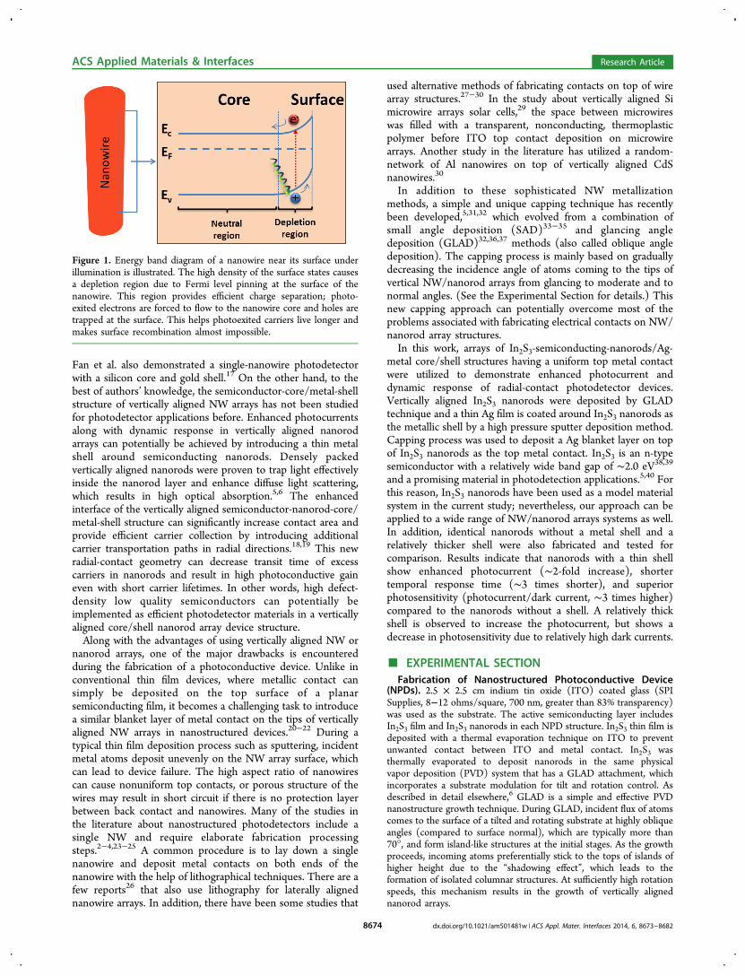
Another superiority of NWs compared to thin filmcounterparts in photodetector applications is their high surfaceto volume ratio, leading to high density of the surface states. Asillustrated in Figure 1, a depletion region due to Fermi levelpinning7 at the surface of the wire can be formed due to thehigh density of the surface states. Some photoexcited carriers inthis region can move toward inside the wire while oppositelycharged ones flow to the surface and get trapped there. Chargecarriers that move toward the NW interior can reach thecurrent-collecting electrode and circulate the device multipletimes before they recombine with the opposite charge carriers
that are trapped at surface states. Thus, an efficient chargeseparation can be maintained and this can result in significantlyreduced surface recombination and prolonged carrier lifetimes.7
In addition, short interelectrode spacing within NWs allowscarriers to transit between electrodes at a faster rate.7 For ahighly light-absorbing material, enhanced photoconductive gaincan be obtained mainly through the combination of prolongedcarrier lifetimes and reduced transit times. However, high gainis usually received at the expense of dynamic response. NWswith long carrier lifetimes typically suffer from long recoverytimes and thus show persistent photocurrents.8−11 Therefore,there is a need for alternative photoconductive device structureapproaches to achieve high gain values while maintaining anappropriate dynamic response.Core−shell nanowire structures were proposed for enhanced
photosensitivity12 and have recently received great attention inphotovoltaic and photodetector applications.13−17 Some ofthese studies utilized semiconductor materials for both core andshell regions,14,15 whereas a few others employed a metal coreand a semiconductor shell16 to build nanowire photodetectors.
Received: March 12, 2014Accepted: May 13, 2014Published: May 13, 2014
Fan et al. also demonstrated a single-nanowire photodetectorwith a silicon core and gold shell.17 On the other hand, to thebest of authors’ knowledge, the semiconductor-core/metal-shellstructure of vertically aligned NW arrays has not been studiedfor photodetector applications before. Enhanced photocurrentsalong with dynamic response in vertically aligned nanorodarrays can potentially be achieved by introducing a thin metalshell around semiconducting nanorods. Densely packedvertically aligned nanorods were proven to trap light effectivelyinside the nanorod layer and enhance diffuse light scattering,which results in high optical absorption.5,6 The enhancedinterface of the vertically aligned semiconductor-nanorod-core/metal-shell structure can significantly increase contact area andprovide efficient carrier collection by introducing additionalcarrier transportation paths in radial directions.18,19 This newradial-contact geometry can decrease transit time of excesscarriers in nanorods and result in high photoconductive gaineven with short carrier lifetimes. In other words, high defect-density low quality semiconductors can potentially beimplemented as efficient photodetector materials in a verticallyaligned core/shell nanorod array device structure.Along with the advantages of using vertically aligned NW or
nanorod arrays, one of the major drawbacks is encounteredduring the fabrication of a photoconductive device. Unlike inconventional thin film devices, where metallic contact cansimply be deposited on the top surface of a planarsemiconducting film, it becomes a challenging task to introducea similar blanket layer of metal contact on the tips of verticallyaligned NW arrays in nanostructured devices.20−22 During atypical thin film deposition process such as sputtering, incidentmetal atoms deposit unevenly on the NW array surface, whichcan lead to device failure. The high aspect ratio of nanowirescan cause nonuniform top contacts, or porous structure of thewires may result in short circuit if there is no protection layerbetween back contact and nanowires. Many of the studies inthe literature about nanostructured photodetectors include asingle NW and require elaborate fabrication processingsteps.2−4,23−25 A common procedure is to lay down a singlenanowire and deposit metal contacts on both ends of thenanowire with the help of lithographical techniques. There are afew reports26 that also use lithography for laterally alignednanowire arrays. In addition, there have been some studies that
used alternative methods of fabricating contacts on top of wirearray structures.27−30 In the study about vertically aligned Simicrowire arrays solar cells,29 the space between microwireswas filled with a transparent, nonconducting, thermoplasticpolymer before ITO top contact deposition on microwirearrays. Another study in the literature has utilized a random-network of Al nanowires on top of vertically aligned CdSnanowires.30
In addition to these sophisticated NW metallizationmethods, a simple and unique capping technique has recentlybeen developed,5,31,32 which evolved from a combination ofsmall angle deposition (SAD)33−35 and glancing angledeposition (GLAD)32,36,37 methods (also called oblique angledeposition). The capping process is mainly based on graduallydecreasing the incidence angle of atoms coming to the tips ofvertical NW/nanorod arrays from glancing to moderate and tonormal angles. (See the Experimental Section for details.) Thisnew capping approach can potentially overcome most of theproblems associated with fabricating electrical contacts on NW/nanorod array structures.In this work, arrays of In2S3-semiconducting-nanorods/Ag-
metal core/shell structures having a uniform top metal contactwere utilized to demonstrate enhanced photocurrent anddynamic response of radial-contact photodetector devices.Vertically aligned In2S3 nanorods were deposited by GLADtechnique and a thin Ag film is coated around In2S3 nanorods asthe metallic shell by a high pressure sputter deposition method.Capping process was used to deposit a Ag blanket layer on topof In2S3 nanorods as the top metal contact. In2S3 is an n-typesemiconductor with a relatively wide band gap of ∼2.0 eV38,39
and a promising material in photodetection applications.5,40 Forthis reason, In2S3 nanorods have been used as a model materialsystem in the current study; nevertheless, our approach can beapplied to a wide range of NW/nanorod arrays systems as well.In addition, identical nanorods without a metal shell and arelatively thicker shell were also fabricated and tested forcomparison. Results indicate that nanorods with a thin shellshow enhanced photocurrent (∼2-fold increase), shortertemporal response time (∼3 times shorter), and superiorphotosensitivity (photocurrent/dark current, ∼3 times higher)compared to the nanorods without a shell. A relatively thickshell is observed to increase the photocurrent, but shows adecrease in photosensitivity due to relatively high dark currents.
■ EXPERIMENTAL SECTIONFabrication of Nanostructured Photoconductive Device
(NPDs). 2.5 × 2.5 cm indium tin oxide (ITO) coated glass (SPISupplies, 8−12 ohms/square, 700 nm, greater than 83% transparency)was used as the substrate. The active semiconducting layer includesIn2S3 film and In2S3 nanorods in each NPD structure. In2S3 thin film isdeposited with a thermal evaporation technique on ITO to preventunwanted contact between ITO and metal contact. In2S3 wasthermally evaporated to deposit nanorods in the same physicalvapor deposition (PVD) system that has a GLAD attachment, whichincorporates a substrate modulation for tilt and rotation control. Asdescribed in detail elsewhere,6 GLAD is a simple and effective PVDnanostructure growth technique. During GLAD, incident flux of atomscomes to the surface of a tilted and rotating substrate at highly obliqueangles (compared to surface normal), which are typically more than70°, and form island-like structures at the initial stages. As the growthproceeds, incoming atoms preferentially stick to the tops of islands ofhigher height due to the “shadowing effect”, which leads to theformation of isolated columnar structures. At sufficiently high rotationspeeds, this mechanism results in the growth of vertically alignednanorod arrays.
Figure 1. Energy band diagram of a nanowire near its surface underillumination is illustrated. The high density of the surface states causesa depletion region due to Fermi level pinning at the surface of thenanowire. This region provides efficient charge separation; photo-exited electrons are forced to flow to the nanowire core and holes aretrapped at the surface. This helps photoexited carriers live longer andmakes surface recombination almost impossible.
ACS Applied Materials & Interfaces Research Article
In2S3 powder (from CERAC) was used as the evaporation sourcematerial. Film and nanorod depositions were held at roomtemperature under 2.0 × 10⁻⁶ mbar base pressure with a depositionrate of 0.2 nm/sec (i.e., nanorod length/deposition time), which wasmeasured by quartz crystal microbalance (QCM) and confirmed bythe analysis of cross-sectional scanning electron microscopy (SEM,JEOL JSM 7000F) images. For nanorod fabrication, samples werepositioned at 85° incidence angle measured between the incident fluxand the substrate normal axis. In2S3 nanorods were deposited rightafter In2S3 thin film growth. After active layer (In2S3 thin film andnanorods) fabrication, samples were taken out of the PVD system andwere applied a vacuum compatible plastic shadowing mask that had 6circular openings (0.08 cm2) on it to form isolated devices on the samesample. After the mask was attached, samples were put back into thesame PVD system to be coated with metal shell and metal capping.For the structures with a metallic shell, nanorods were coated with
Ag by sputtering at high pressure, which is a well-known and widelyused technique in the literature, especially in gold coaters for SEMsystems. The working gas (Ar) pressure was set to 3.0 × 10⁻² mbar inorder to achieve a conformal-like metal shell around the nanorods.For the metal capping, the Ar pressure was reduced to 3.0 × 10⁻³
mbar, and Ag was sputter deposited on top of nanorods by using anovel capping process. As illustrated in Figure 2, the initial stage of thecapping process is basically deposition at glancing angles (i.e., GLAD).Incident flux of metal atoms comes to the substrate surface at a highangle and starts to stick to the tips of the predeposited vertically
aligned In2S3 nanorod arrays. They continue to grow in the verticaldirection due to the combination of shadowing effect and substraterotation. Then the tilt angle was gradually decreased at a rate of 2°/min and brought the growth a small angle deposition (SAD)regime.33−35 During the SAD stage, atoms can reach to the sides ofthe tiny metallic nanorods that are formed at the initial GLAD stage.As illustrated in Figure 2, tiny metallic nanorods evolve to taperedcone-like structures during the intermediate SAD stage of cappingprocess. At small angles, structures start to merge together to form auniform blanket layer on top of vertically aligned nanorods. The finalstage of the capping process (Figure 2) includes conventionaldeposition at normal angle to introduce a continuous metal film. Inthis study, Ag was deposited at normal angle for 5 min and about a 700nm thick metallic layer is formed during deposition (total depositiontime including capping is 45 min).
Preparation of TEM Samples. In2S3 nanorods were deposited onSi substrates under the same experimental conditions used in NPDpreparation. Then In2S3 nanorods were coated with thin and thick Aglayers in separate depositions with the same deposition technique(high pressure sputtering) and same parameters used for Ag shells inNPDs. After that, Ag coated In2S3 nanorods were scribed off from Sisubstrate onto TEM grids in order to be analyzed under TEM.
Morphological Characterization. Morphological characteriza-tion of Ag covered In2S3 nanorods was done by scanning electronmicroscopy (SEM, JEOL JSM 7000F) and transmission electronmicroscopy (TEM, JEOL JEM 2100F). All STEM/EDS images weretaken by a 1.5 nm beam size at 80 kV.
Photoconductivity Experiments. A Keithley 2400 sourcemeterwith two probes was used for electrical characterization. A laser diodeat a 532 nm wavelength (Roithner LaserTechnik, CW 532-005F) wasused as a light source in photocurrent measurements. The incidencelight intensity was 3 mW/cm2. A BK Precision 1788 programmableDC power supply was used to control the light source, which wasturned on and off in 10 s time intervals.
■ RESULTS AND DISCUSSION
As-deposited thin film and GLAD nanorods of indium sulfidewere found to be stoichiometric In2S3, yet with an amorphousstructure.5 Figure 3a illustrates the device structure without themetal shell, and Figure 3b,c demonstrates the radial-contactNPD structures with relatively thin and thick metallic shellsaround nanorods, respectively. Figure 3d−f shows SEM imagesof the NPD structures, which were produced to correspond todevice structures of Figure 3a−c, respectively. Figure 3d showsthe Ag cap layer, In2S3 nanorods, and In2S3 thin film on ITOcoated glass substrate (top to bottom) and the inset indicates ahigher resolution SEM image that allows the nanorods and filmappear clearly.The height of the In2S3 nanorods was measured as 198 ± 12
nm and bottom In2S3 film thickness was found to be 57 ± 4 nmby analyzing SEM images. Figure 3e,f shows In2S3 nanorodswith a Ag metal shell and underlying In2S3 thin film on the Sisubstrate (the Ag cap layer was peeled off for convenience). Weused SEM images of In2S3 nanorods with a Ag metal shellgrown on Si instead of ITO coated glass substrate forconvenience of Si substrates during SEM sample preparation.However, we observed that there is no morphologicaldifference in nanorods on Si substrate and the nanorodsgrown on ITO coated glass substrate, as can be seen in FigureS1b,c (see the Supporting Information). The capping processforms a continuous top metal film (indicated by two-sidedarrow) of about 700 nm in thickness, shown in Figure S1a (seethe Supporting Information).Assuming the shape of the nanorods are perfect cylinders and
given that the material filling ratio of nanorods (0.7) and Agdeposition rate (30 nm/min), we calculated the estimated
Figure 2. Stages of metal capping process are illustrated. At early stageof the deposition, incident flux comes to the substrate plane at highangles of 70° ≤ θ ≤ 85° (glancing angle deposition, GLAD) andcontinues to form columnar metal contacts on top of nanorods. Atintermediate stages, flux approaches at relatively small angles of 0° < θ< 70° (small angle deposition, SAD), and that allows atoms to depositon sides of columnar structure leading to a lateral growth. As thedeposition angle is gradually decreased, columnar metal featurescoalesce and start to form a continuous film. At the final stage, themetal is deposited at normal angle incidence to form a uniform blanketthin film.
ACS Applied Materials & Interfaces Research Article
thicknesses of Ag thin and thick shells as 1.9 ± 0.1 nm and 3.8± 0.2 nm, respectively. As seen in Figure 3e,f, shapes of In2S3nanorods coated with the Ag shell remained same as the bareones (Figure 3d), which is thought to be an indication ofconformal Ag deposition. To investigate the Ag shell’sconformality in more detail and measure the shell thicknessmore accurately, transmission electron microscopy (TEM) andscanning transmission electron microscopy/energy dispersivespectroscopy (of X-ray) (STEM/EDS) analyses were per-formed and the results are shown in Figure 4. For TEM andSTEM/EDS analyses, In2S3 nanorods were deposited on bareSi wafers and covered with thin and thick Ag shells underidentical experimental conditions as in the deposition of NPDsof this study, which are described above.A cluster of In2S3 nanorods coated with a thin Ag shell can be
seen in Figure 4a. Top and bottom portions of an individualnanorod from this cluster are shown in Figure 4b,c,respectively. The thin Ag shell is measured to be about 2.04± 0.61 nm (see the Supporting Information for details) fromFigure 4b,c where arrows indicate the thin Ag layer. BecauseIn2S3 nanorods in this study are amorphous, no crystal structureis expected to be observed in TEM images. However, anordered atomic structure can be easily seen in Figure 4b even atthe bottom of the nanorod covered with thin Ag layer. This is
believed to be a strong indication of uniform Ag coveragearound In2S3 nanorods. Figure 4d shows a STEM image of the
Figure 3. Schematics and SEM images for photoconductive devicestructures are illustrated. (a) Nanostructured photoconductive device(NPD) structure (control sample, without metallic shell), (b) NPDstructure with a thin metallic shell, (c) NPD structure with a relativelythick metallic shell, (d) SEM image of vertically aligned In2S3 nanorodarrays and underlying In2S3 film on ITO coated glass substrate, with aAg metallic capping layer on top of nanorods, (e) SEM image of In2S3nanorods coated with thin Ag shell and In2S3 film on Si substrate, (f)SEM image of In2S3 nanorods coated with a relatively thicker Ag shelland In2S3 film on Si substrate. The Ag capping layer was peeled off forpanels e and f.
Figure 4. TEM and STEM/EDS images for Ag coated In2S3 nanorodsare shown. (a) TEM image of a cluster of In2S3 nanorods coated with athin Ag shell (scale bar 20 nm), (b) top portion of an individual Agcoated In2S3 nanorod (arrows indicate the thin Ag layer, scale bar 5nm), (c) bottom portion of an individual Ag coated In2S3 nanorod(arrows indicate the Ag layer thickness and ordered atomic structureshows uniform coverage of crystalline Ag around amorphous In2S3nanorods, scale bar 5 nm), (d) STEM image of a cluster of In2S3nanorods coated with a thin Ag shell and EDS indicating the existenceof In, S, and Ag throughout the whole nanorod, (e) TEM image of acluster of In2S3 nanorods coated with a thick Ag shell (scale bar 20nm), (f) top portion of an individual Ag coated In2S3 nanorod (arrowsindicate the thick Ag layer, scale bar 5 nm), (g) STEM image of acluster of In2S3 nanorods coated with thick Ag shell and EDSindicating uniform distribution of In, S, and Ag along the nanorod.
ACS Applied Materials & Interfaces Research Article
same cluster of nanorods and associated EDS results indicatingthe existence of In, S, and Ag throughout the nanorods. It isobvious that Ag is detected along the whole nanorod.Figure 4e has a TEM image of a group of In2S3 nanorods
with thick Ag film. The top portion of an individual nanorodwith a high magnification is also shown in Figure 4f with arrowspointing the thick Ag shell, which is measured to be about 3.89± 0.47 nm (see the Supporting Information for details). Thethick shell is found to be almost ∼2 times thicker than the thinshell, which is consistent with the deposition times (i.e., thedeposition time of thick shell was 1 min, two times longer thanthe deposition time of thin shell, which was 30 s). In addition,our estimated shell thicknesses agree well with measuredthicknesses from TEM analysis. STEM image and EDS resultsfor In2S3 nanorods with thick Ag shell are also shown in Figure4g, indicating the uniform distribution of In, S, and Ag alongthe nanorods.For electrical characterization, we studied current−voltage
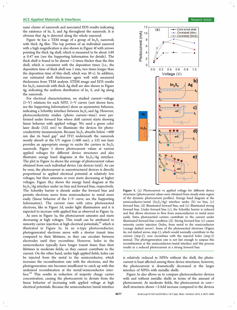
(I−V) relations for each NPD. I−V curves (not shown here,see the Supporting Information) show an asymmetric behavior,indicating a Schottky interface between In2S3 and Ag. However,photoconductivity studies (photo current−time) were per-formed under forward bias where drift current starts showinglinear behavior with applied voltage. We used a green colorlaser diode (532 nm) to illuminate the devices for photo-conductivity measurements. Because In2S3 absorbs below ∼600nm due its band gap5 and ITO underneath the nanorodsmostly absorb at the UV region (<400 nm); a 532 nm laserprovides an appropriate energy to excite the carriers in In2S3nanorods. Figure 5 shows photocurrent values at variousapplied voltages for different device structures and alsoillustrates energy band diagrams at the In2S3/Ag interface.The plot in Figure 5a shows the average of photocurrent valuesobtained from each individual device (six devices total). As canbe seen, the photocurrent in nanostructured devices is directlyproportional to applied electrical potential at relatively lowvoltages, but then saturates or even starts decreasing at highervoltages. Figure 5b,c shows the energy band diagram at theIn2S3/Ag interface under no bias and forward bias, respectively.The Schottky barrier is shrunk under the forward bias andpermits electrons move from semiconductor to metal moreeasily (linear behavior of the I−V curve, see the SupportingInformation). The current rises with extra photoexcitedelectrons, like in Figure 5d, under light illumination and it isexpected to increase with applied bias as observed in Figure 5a.As seen in Figure 5a, the photocurrent saturates and starts
decreasing at high voltages. This result can be attributed tominority carrier injection at high electrical potentials,41 which isillustrated in Figure 5e. In an n-type photoconductor,photogenerated electrons move with a shorter transit timecompared to their lifetimes, so they can circulate betweenelectrodes until they recombine. However, holes in thesemiconductor typically have longer transit times than theirlifetimes in moderate fields, so they cannot contribute to thecurrent. On the other hand, under high applied fields, holes canbe injected from the metal to the semiconductor, whichincreases the recombination rate with the electrons, and thephotogeneration rate becomes insufficient to catch up with thisundesired recombination at the metal/semiconductor inter-face.42 This results in reduction of majority charge carrierconcentration, causing the photocurrent to deviate from thelinear behavior of increasing with applied voltage at highelectrical potentials. Because the semiconductor/metal interface
is relatively reduced in NPDs without the shell, the photo-current is least affected among three device structures; however,the photocurrent is dramatically decreased at the largerinterface of NPDs with metallic shells.Figure 5a also allows us to compare photoconductor devices
with and without metallic shells in terms of the amount ofphotocurrent. At moderate fields, the photocurrent in core−shell structures shows ∼2-fold increase compared to the devices
Figure 5. (a) Photocurrent vs applied voltage for different devicestructures (photocurrent values were obtained from steady-state regionof the dynamic photocurrent profiles). Energy band diagram at thesemiconductor/metal (In2S3/Ag) interface under (b) no bias, (c)forward bias, (d) illuminated forward bias, and (e) illuminated strongforward bias. Under forward bias (c), the Schottky barrier is reducedand that allows electrons to flow from semiconductor to metal moreeasily. Extra photoexcited carriers contribute to the current underilluminated forward bias condition (d). Strong forward bias (e) causesminority carrier injection (holes, from metal to the semiconductor(orange dashed arrow). Some of the photoexcited electrons (Figure4e, red dashed arrow, step-1), which would normally contribute to thecurrent (step-2), now recombine with the injected holes (step-3)instead. The photogeneration rate is not fast enough to surpass thisrecombination at the semiconductor/metal interface and this processresults in a reduced photocurrent at a strong forward bias.
ACS Applied Materials & Interfaces Research Article
without the shell. The photocurrent could have been enhancedwith excess photoexcitation due to higher optical absorption ofthe device with a metallic shell. However, UV−vis-NIRspectroscopy (with integrating sphere) measurements (seethe Supporting Information) indicate that device structureswith and without a metal shell absorb light at similar rates (e.g.,∼86% at a 532 nm wavelength). Thus, enhancement inphotocurrent can be attributed to reduced transit times, whichare thought to be due to shorter interelectrode distances innanostructured devices with metallic shells. We propose thatmetallic shells around nanorods help the excess carriers totransit in a short amount of time by introducing alternativepathways in radial directions in addition to the vertical directionalong the nanorods. Furthermore, keeping the metal shellthickness small does not seem to have an adverse effect on theoverall optical absorption in nanorods, which contributesachieving a high photoconductive gain.To examine the dynamic behavior of the photocurrent in
detail, current was measured as a function of time for each ofthe six individual devices and the average of the data wasplotted for each NPD after subtracting associated dark currents.Figure 6a indicates time dependence of the photocurrent for
each NPD at 0.1 V bias while the light source was turned onand off at 10 s time intervals. As seen from Figure 6a, NPDswith a thin metal shell show an enhanced photocurrent (∼2-fold increase) compared to NPDs without a metal shell.Similarly, higher photocurrent values were obtained from NPDswith a relatively thick shell compared to other two structures.Enhancement in photocurrent can be attributed to two possiblereasons: one is an increase in optical absorption and the secondone is efficient carrier transportation and collection. Asmentioned above, optical power absorbed in all NPDs wassimilar to each other. However, UV−vis-NIR spectroscopymeasurement results represent optical absorption in the wholedevice including metal and semiconducting layers. On the otherhand, given the fact that loss of light in metals occurs at muchsmaller rates compared to light absorption in semiconductingmaterials, and the metal shell thicknesses in our study are
estimated to be in the range of about 2−5 nm, we do notexpect a significant change in the amount of the light absorbedin the In2S3 regions of different NPDs we used.Another possible reason for the enhancements in photo-
current can be due to the improved charge carrier collection. Ifthe excess carriers have longer lifetimes than their transit time,they can make more than one circulation through the deviceuntil recombination takes place. Therefore, longer lifetimes orshorter transit times can both enhance the photocurrent. Toextract photo carrier lifetime, photocurrent decays in Figure 6a(i.e., the sections of the profiles right after the light is turnedoff) were fitted with an exponential equation that has twodecaying components:
= +τ τ− −I A Ae et t1
/2
/fast slow (1)
where τfast and τslow are the time constants for fast and slowdecaying of photocurrent profiles, indicating at least two traplevels. We obtained weight-averaged fast and slow timeconstants from each decay portions of the profiles shown inFigure 6a. We extracted carrier lifetime from the mean ofweight-averaged time constants for each NPD (see theSupporting Information for details). Thus, carrier lifetimeswere calculated as 1.07, 0.58, and 0.68 s for NPDs without ametal shell, with a thin metal shell, and with a thick metal shell,respectively. Photo carrier lifetimes for NPDs with a metal shellare found to be lower than NPDs without a shell. However, itcan be seen that NPDs with a metal shell had a higherphotocurrent response at 0.1 V compared to the one without ashell, although its photo carrier lifetimes were much smaller.The second parameter that can play an important role in
enhancing photocurrent is carrier transit time, which mainlydepends on carrier mobility and interelectrode separation. Theratio of carrier lifetime and carrier transit time gives the amountof photoconductive gain, which is defined as number of excesselectrons per number of absorbed photons. This definition canbe rewritten as
ω=
ℏG
I
P
/e
/ph
abs (2)
where G is the photoconductive gain, Iph is the photocurrent, eis one electron charge, Pabs is the absorbed optical power, andℏω is the energy of one photon. According to this relation,photoconductive gain values at 0.1 V for NPDs without a shell,with a thin shell, and with a thick shell were calculated as 24.15,44.36, and 61.06 and corresponding transit times werecalculated as 4.44 × 10⁻², 1.3 × 10⁻², and 1.1 × 10⁻² s,respectively. Carrier transit times for NPDs with a metal shellare very close to each other and ∼4 times shorter than transittime of carriers in NPDs without a shell. Therefore, despite thereduced charge carrier lifetimes, NPDs with a metal shell showa high photocurrent response, mainly due to the short transittimes achieved by the core−shell geometry.High surface to volume ratio in nanowire/nanorod structures
compared to thin film counterparts increase surface states,which are believed to be the main reason for prolongedlifetimes in nanowire/nanorod structures.7 In2S3 nanorods werealready shown to have higher photoresponse than their thinfilm counterparts.5 In the current study, results from theanalysis of photocurrent decay reveal that thin metal shellaround nanorods shortens the carrier lifetime. This resultsuggests that thin metal shell may passivate dangling bonds onthe surface of the nanorods and thus decrease the amount of
Figure 6. Dynamic photocurrent profiles as the light is turned on(plateaus) and off (valleys) for an applied bias of (a) 0.1 and (b) 0.5 V.
ACS Applied Materials & Interfaces Research Article
surface states. Therefore, shortening of carrier lifetime may be aresult of less surface states.Figure 6b shows a comparison of photocurrent profiles
among each NPD as a function of time at 0.5 V applied voltage.As seen in Figure 6b, transient photocurrent spikes areobserved for NPDs with a metal shell. However, the shape ofthe spike in NPDs with a thin metal shell is sharper than theone in NPDs with a thick metal shell. Initially, the photocurrentreaches its peak value in a very short time (∼0.24 s), but thenstarts decaying and shows a steady-state behavior after a while.A transient photocurrent under illumination is believed to bedue to trap states (i.e., defects) at the metal/semiconductorinterface.43 Although there is a strong indication of surfacepassivation by the metal, defect formation at the semi-conductor/metal interface is inevitable during metal shelldeposition. Such defects can act like trap states for photoexcitedcarriers (surface states in In2S3 nanorods without a shell, whichwas described above, were traps for holes such that electronscould move to electrodes easily). Defects at semiconductor/metal interface can also exist in In2S3 nanorods without a shell(interface between Ag cap layer and the tips of the In2S3nanorods); however, the photocarrier generation rate over-comes such traps, which are believed to be very limitedcompared to the ones in Ag coated In2S3 nanorods (due to highsurface area). Magnitudes of the transient photocurrent inFigure 6b are observed to be decreasing in time. This indicatesthat a number of electrons trapped in the defects after the firstlight pulse stay trapped and do not contribute to thephotocurrent for the second pulse.44 Therefore, the peakcurrent becomes lower after the second pulse of light. Trappedelectrons need more time than the light pulse interval used inthis study (10 s) to be completely released and maintain thesame peak current for each pulse.Although carrier lifetime is shortened in In2S3 nanorods with
a metal shell, existence of the metal shell helps carriers reachthe electrode faster compared to the case without a metal shell.Thus, carriers can circulate multiple times through the deviceand lead to enhanced gain even with shorter lifetimes. On theother hand, shortening lifetime also helps device to providefaster dynamic response. In Table 1, temporal response, whichis defined as the time it takes for the photocurrent to dropdown to 90% of its initial value during the decay period after
the light is turned off, are shown along with other parametersfor each NPD at various applied bias values. For example, thetemporal response time for NPDs with a thinner metal shell at0.1 V was calculated to be 1.05 s. This is about 3 times shorterthan the one for NPDs without a shell, which is believed to bedue to the shorter times for recombination in NPDs with a thinmetallic shell. While NPDs without a shell show persistentphotocurrents, a metal shell allows the photocurrent todiminish easily with the help of short carrier lifetimes. Theseresults demonstrate that an enhanced photocurrent along withfaster dynamic response can be accomplished in one photo-detector device at the same time by introducing a thin metalshell around the nanorod.Figure 7 presents the results for photosensitivity (the ratio of
photocurrent to dark current) for each NPD at different appliedbias values, and also its dynamic change at 0.1 and 0.5 V as thelight is sequentially turned on and off. As can be seen in Figure7a, all NPDs show a similar trend: high photosensitivity at lowvoltages that drastically decreases with increased applied bias.One of the reasons of this behavior can be attributed to the lowphotocurrents at relatively high fields due to the effect ofminority carrier injection, which was explained above. Anotherreason is the high dark current values at higher voltages. Ifphotosensitivity among NPDs is compared with each other,one can see that NPDs with a thin metal shell are ∼3-fold and∼1.5-fold more sensitive to the light compared to NPDswithout a shell and NPDs with a relatively thick metal shell,respectively.Figure 7b,c indicates dynamic photosensitivity response for
each NPD at 0.1 and 0.5 V, respectively, as the light issequentially turned on and off. The overall behavior of dynamicphotosensitivity profiles at 0.5 V plotted in Figure 7c seemssimilar to the photocurrent response observed in Figure 6b.This is an expected result, as photosensitivity is linearlyproportional to photocurrent. However, we cannot see thesimilar correlation between photocurrent responses andphotosensitivity at 0.1 V in Figures 6a and 7b, respectively.Although NPDs with a thick shell have a higher photocurrent at0.1 V applied bias, their photosensitivity is drastically lowerthan the sensitivity of NPDs with a thin shell, as seen in Figure7b.
Table 1. Dark Current, Photocurrent, Photosensitivity (Photocurrent/Dark Current), Temporal Response Time, Gain, andResponsivity (Photocurrent/Optical Power) Values Listed for Each NPD at 0.025, 0.1, 0.25, 0.5, and 1 V Applied Bias andunder 532 nm Wavelength Light with an Intensity of 3 mW/cm2
applied bias (V) structures dark current (Id) (mA) photo current (Iph) (mA) Iph\Id (%) temporal response time (s) gain responsivity (A/W)
Enhanced sensitivity of NPDs with a thin metal shellcompared to NPDs without a shell is expected and can beexplained due to enhanced photocurrent in this structure, asseen in Figure 5a. On the other hand, despite their highphotocurrents (especially at low voltages), NPDs with a thickmetal shell are less sensitive compared to NPDs with a thinmetal shell. This enhanced photosensitivity in NPDs with a thinmetal shell is mainly due to its low dark current. However,introducing metal around nanorods is normally expected todecrease the total resistance, hence increasing the dark currentpassing through device. As seen from Figure 8a, this is the casefor NPDs with a relatively thick metal shell. Dark current valuesat different applied voltages for NPDs with a thick shell arehigher than dark current values for NPDs without a metal shell.On the other hand, lower dark current values were measuredfor NPD with a thin metallic shell, even lower compared toNPDs without a shell. This unexpected result can be attributedto microstructural effects introduced during high pressuresputter deposition of the Ag shell.As shown in Figure 8b, incoming flux of Ag atoms at high
pressure sputter deposition has a wider angular distribution.Therefore, some of the incoming atoms can come to the topsurface of nanorods at high angles (indicated as 1 in Figure 8b)and can disrupt uniform structure and cause columnar structureformation due to local shadowing effect. In addition, incidentatoms coming to the surface at normal and near-normal anglesreach the side walls of the nanorods at high angles (indicated as2 in Figure 8b). They can form columnar structures on the sidewalls also due to the shadowing effect. Therefore, a slightly
noncontinuous columnar coating around nanorods is thoughtto be formed, which can result in highly resistive spots in NPDswith a thin metallic shell. On the other hand, as the growthcontinues, columns can merge and form a more continuousfilm microstructure, as in the case of NPDs with a thicker shell,which can explain the higher dark current values observed.Therefore, although a thin metal shell lacks high uniformity andhence shows high resistance, this property turns out to be anadvantage in photodetector applications of photoconductorswhere low dark current values are desired.High dark resistance of a thin shell also affects the behavior
of the photocurrent. NPDs with a thin shell produce lowerphotocurrents than NPDs with a thick shell at moderateapplied bias (Figure 5a). We propose that this is due to lowresistance of a thick shell as a result of high film uniformity. Onthe other hand, photocurrent values of NPDs with a thick shellget lower than the photocurrent produced by NPDs with a thinshell under strong forward bias. We propose that low resistanceof NPDs with a thick shell causes higher minority carrierinjection than that of NPDs with a thin shell, which causes a
Figure 7. (a) Photosensitivity (the ratio of photocurrent to darkcurrent) at different applied voltages. Dynamic photosensitivityresponse for each NPD structure at (b) 0.1 V and (c) 0.5 V.
Figure 8. (a) Dark current values at various applied bias for each NPD.NPDs with a thin metal shell show lower dark currents compared tothe NPDs with a thicker shell. (b) Wider angular distribution ofincident flux at high pressure sputter deposition is illustrated on theleft. A zoom-out image of the corner of a nanorod with a metal shell isshown on the right side of the schematic. Atoms that come at obliqueangles to the tips of nanorod (indicated as 1) form a columnarstructure due to local shadowing effect. Atoms that are able to reach tothe side walls of the nanorods (indicated as 2) mainly come at obliqueangles with respect to local surface normal. Obliquely coming flux canform a columnar structure also at the side walls of nanorods. Thisnoncontinuous coating can result in high resistance and hence lowerdark current values in NPDs with a thin metal shell.
ACS Applied Materials & Interfaces Research Article
more notable decrease in the photocurrent of NPDs with thethick shell.
■ CONCLUSION
Nanostructured photodetector devices made of verticallyaligned indium sulfide nanorod arrays were proven to haveenhanced photocurrents along with improved dynamicresponse by introducing a thin silver metal shell aroundnanorods. Identical In2S3 nanorods without a metal shell and arelatively thick shell were also fabricated and characterized forcomparison. Results indicate that the nanorods with a thinmetal shell show enhanced photocurrent (∼2-fold increase)and photosensitivity (∼3 times higher) compared to thenanorods without a metal shell. A thin metal shell is thought topassivate the surface states, which in turn reduces the carrierlifetimes and results in superior dynamic response compared tonanorods without a shell. On the other hand, reduced carriertransit time due to short interelectrode spacing compensatesthe disadvantage of short carrier lifetime and gives rise to theenhanced photoconductive gain and photocurrent. In addition,low dark current values observed in nanorods with a thin metalshell, which is believed to be due to columnar microstructureformed during high pressure sputter deposition of Ag, have ledto improved photosensitivity response of the photodetector.On the other hand, a relatively thicker metal shell caused higherdark currents due to a more continuous film microstructure,which resulted in lower photosensitivity response compared tothe device with a thinner shell. Our results demonstrate thathigh photoconductive gain and fast dynamic response can beaccomplished in a given device at the same time, even for theones made of low quality materials with high defect densities.We propose that our simple device fabrication route, which
includes nanostructure layer formation with GLAD, conformalcoating by high pressure sputter deposition, and a uniquecapping process (combination of SAD and GLAD) for top-contact formation, is a promising alternative for potentialapplications such as detectors, sensors, and imaging devices.Although the device size reported here (0.08 cm2) is smallenough on a research scale but quite large for some potentialapplications, one can consider lithographical techniques to formsmaller isolated devices in order to get dense micro/nanoarrays.
■ ASSOCIATED CONTENT
*S Supporting InformationAdditional SEM images of NPDs without a shell; Ag shellthickness measurement with TEM Analysis; I−V curves ofNPD under dark and illuminated conditions; estimation ofcarrier lifetimes by photocurrent decays. This material isavailable free of charge via the Internet at http://pubs.acs.org.
Author ContributionsThe paper was written through contributions of all authors. Allauthors have given approval to the final version of the paper.
NotesThe authors declare no competing financial interest.
■ ACKNOWLEDGMENTS
This work was supported by NASA (grant no: NNX09AW22A)and NSF (grant numbers: EPS-1003970 and 1159830). Theauthors thank UALR Center for Integrative NanotechnologySciences for helping with SEM images and UV−vis measure-ments.
■ REFERENCES(1) Zhai, T. Y.; Fang, X. S.; Liao, M. Y.; Xu, X. J.; Zeng, H. B.;Yoshio, B.; Golberg, D. A Comprehensive Review of One-DimensionalMetal-Oxide Nanostructure Photodetectors. Sensors-Basel 2009, 9 (8),6504−6529.(2) Law, J. B. K.; Thong, J. T. L., Simple Fabrication of a ZnONanowire Photodetector with a Fast Photoresponse Time. Appl. Phys.Lett. 2006, 88 (13).(3) Zhai, T. Y.; Fang, X. S.; Liao, M. Y.; Xu, X. J.; Li, L.; Liu, B. D.;Koide, Y.; Ma, Y.; Yao, J. N.; Bando, Y.; Golberg, D. Fabrication ofHigh-Quality In2Se3 Nanowire Arrays toward High-PerformanceVisible-Light Photodetectors. ACS Nano 2010, 4 (3), 1596−1602.(4) Soci, C.; Zhang, A.; Xiang, B.; Dayeh, S. A.; Aplin, D. P. R.; Park,J.; Bao, X. Y.; Lo, Y. H.; Wang, D. ZnO Nanowire UV Photodetectorswith High Internal Gain. Nano Lett. 2007, 7 (4), 1003−1009.(5) Cansizoglu, M. F.; Engelken, R.; Seo, H. W.; Karabacak, T. HighOptical Absorption of Indium Sulfide Nanorod Arrays Formed byGlancing Angle Deposition. ACS Nano 2010, 4 (2), 733−740.(6) Cansizoglu, H.; Cansizoglu, M. F.; Finckenor, M.; Karabacak, T.Optical Absorption Properties of Semiconducting Nanostructures withDifferent Shapes. Adv. Opt. Mater. 2013, 1 (2), 158−166.(7) Soci, C.; Zhang, A.; Bao, X. Y.; Kim, H.; Lo, Y.; Wang, D. L.Nanowire Photodetectors. J. Nanosci. Nanotechnol. 2010, 10 (3),1430−1449.(8) Calarco, R.; Marso, M.; Richter, T.; Aykanat, A. I.; Meijers, R.;Hart, A. V.; Stoica, T.; Luth, H. Size Dependent Photoconductivity inMBE Grown GaN Nanowires. Nano Lett. 2005, 5 (5), 981−984.(9) Han, S.; Jin, W.; Zhang, D. H.; Tang, T.; Li, C.; Liu, X. L.; Liu, Z.Q.; Lei, B.; Zhou, C. W. Photoconduction Studies on GaN NanowireTransistors under UV and Polarized UV Illumination. Chem. Phys. Lett.2004, 389 (1−3), 176−180.(10) Salfi, J.; Philipose, U.; de Sousa, C. F.; Aouba, S.; Ruda, H. E.Electrical Properties of Ohmic Contacts to ZnSe Nanowires and TheirApplication to Nanowire-Based Photodetection. Appl. Phys. Lett. 2006,89 (26), 261112−261112-3.(11) Park, J.; Lee, E.; Lee, K. W.; Lee, C. E. Electrical Transport andQuasipersistent Photocurrent in Vanadium Oxide Nanowire Net-works. Appl. Phys. Lett. 2006, 89 (18), 183114−183114-3.(12) Hayden, O.; Agarwal, R.; Lieber, C. M. Nanoscale AvalanchePhotodiodes for Highly Sensitive and Spatially Resolved PhotonDetection. Nat. Mater. 2006, 5 (5), 352−356.(13) Adachi, M. M.; Anantram, M. P.; Karim, K. S. Optical Propertiesof Crystalline-Amorphous Core-Shell Silicon Nanowires. Nano Lett.2010, 10 (10), 4093−4098.(14) Wang, K.; Chen, J. J.; Zeng, Z. M.; Tarr, J.; Zhou, W. L.; Zhang,Y.; Yan, Y. F.; Jiang, C. S.; Pern, J.; Mascarenhas, A. Synthesis andPhotovoltaic Effect of Vertically Aligned ZnO/ZnS Core/ShellNanowire Arrays. Appl. Phys. Lett. 2010, 96 (12), 123105−123105-3.(15) Gallo, E. M.; Chen, G. N.; Currie, M.; McGuckin, T.; Prete, P.;Lovergine, N.; Nabet, B.; Spanier, J. E. Picosecond Response Times inGaAs/AlGaAs Core/Shell Nanowire-based Photodetectors. Appl. Phys.Lett. 2011, 98 (24), 241113−241113-3.(16) Hsu, C. Y.; Lien, D. H.; Lu, S. Y.; Chen, C. Y.; Kang, C. F.;Chueh, Y. L.; Hsu, W. K.; He, J. H. Supersensitive, Ultrafast, andBroad-Band Light-Harvesting Scheme Employing Carbon Nanotube/TiO2 Core-Shell Nanowire Geometry. ACS Nano 2012, 6 (8), 6687−6692.(17) Fan, P. Y.; Chettiar, U. K.; Cao, L. Y.; Afshinmanesh, F.;Engheta, N.; Brongersma, M. L. An Invisible Metal-SemiconductorPhotodetector. Nat. Photonics 2012, 6 (6), 380−385.
ACS Applied Materials & Interfaces Research Article
(18) Kelzenberg, M. D.; Putnam, M. C.; Turner-Evans, D. B.; Lewis,N. S.; Atwater, H. A. Predicted Efficiency of Si Wire Array Solar Cells.34th IEEE Photovoltaic Specialists Conference (PVSC), Philadelphia, PA,June 7−12, 2009; pp 001948−001953.(19) Kelzenberg, M. D.; Boettcher, S. W.; Petykiewicz, J. A.; Turner-Evans, D. B.; Putnam, M. C.; Warren, E. L.; Spurgeon, J. M.; Briggs, R.M.; Lewis, N. S.; Atwater, H. A. Enhanced Absorption and CarrierCollection in Si Wire Arrays for Photovoltaic Applications. Nat. Mater.2010, 9 (4), 368−368.(20) Kim, C. H.; Myung, Y.; Cho, Y. J.; Kim, H. S.; Park, S. H.; Park,J.; Kim, J. Y.; Kim, B. Electronic Structure of Vertically Aligned Mn-Doped CoFe2O4 Nanowires and Their Application as HumiditySensors and Photodetectors. J. Phys. Chem. C 2009, 113 (17), 7085−7090.(21) Kushwaha, A.; Aslam, M. Defect Induced High Photocurrent inSolution Grown Vertically Aligned ZnO Nanowire Array Films. J.Appl. Phys. 2012, 112 (5), 054316−054316-7.(22) Chinnamuthu, P.; Dhar, J. C.; Mondal, A.; Bhattacharyya, A.;Singh, N. K. Ultraviolet Detection using TiO2 Nanowire Array with AgSchottky Contact. J. Phys. D: Appl. Phys. 2012, 45 (13), 135102.(23) Heo, Y. W.; Kang, B. S.; Tien, L. C.; Norton, D. P.; Ren, F.; LaRoche, J. R.; Pearton, S. J. UV Photoresponse of Single ZnONanowires. Appl. Phys. A: Mater. Sci. Process. 2005, 80 (3), 497−499.(24) Chen, L. C.; Huang, H. M.; Chen, R. S.; Chen, H. Y.; Liu, T. W.;Kuo, C. C.; Chen, C. P.; Hsu, H. C.; Chen, K. H.; Yang, Y. J.Photoconductivity in Single AlN Nanowires by Subband GapExcitation. Appl. Phys. Lett. 2010, 96 (6), 062104−062104-3.(25) Gu, Y.; Romankiewicz, J. P.; David, J. K.; Lensch, J. L.; Lauhon,L. J.; Kwak, E. S.; Odom, T. W. Local Photocurrent Mapping as aProbe of Contact Effects and Charge Carrier Transport in Semi-conductor Nanowire Devices. J. Vac. Sci. Technol., B: Microelectron.Nanometer Struct.−Process., Meas., Phenom. 2006, 24 (4), 2172−2177.(26) Peng, S. M.; Su, Y. K.; Ji, L. W.; Wu, C. Z.; Cheng, W. B.; Chao,W. C. ZnO Nanobridge Array UV Photodetectors. J. Phys. Chem. C2010, 114 (7), 3204−3208.(27) Senanayake, P.; Hung, C. H.; Shapiro, J.; Lin, A.; Liang, B. L.;Williams, B. S.; Huffaker, D. L. Surface Plasmon-Enhanced NanopillarPhotodetectors. Nano Lett. 2011, 11 (12), 5279−5283.(28) Senanayake, P.; Lin, A.; Mariani, G.; Shapiro, J.; Tu, C.; Scofield,A. C.; Wong, P. S.; Liang, B. L.; Huffaker, D. L. Photoconductive Gainin Patterned Nanopillar Photodetector Arrays. Appl. Phys. Lett. 2010,97 (20), 203108−203108-3.(29) Putnam, M. C.; Boettcher, S. W.; Kelzenberg, M. D.; Turner-Evans, D. B.; Spurgeon, J. M.; Warren, E. L.; Briggs, R. M.; Lewis, N.S.; Atwater, H. A. Si Microwire-Array Solar Cells. Energy Environ. Sci.2010, 3 (8), 1037−1041.(30) Azulai, D.; Givan, U.; Shpaisman, N.; Belenkova, T. L.; Gilon,H.; Patolsky, F.; Markovich, G. On-Surface Formation of MetalNanowire Transparent Top Electrodes on CdSe Nanowire Array-Based Photoconductive Devices. ACS Appl. Mater. Interfaces 2012, 4(6), 3157−3162.(31) Xi, J. Q.; Kim, J. K.; Schubert, E. F.; Ye, D. X.; Lu, T. M.; Lin, S.Y.; Juneja, J. S. Very Low-Refractive-Index Optical Thin FilmsConsisting of an Array of SiO2 Nanorods. Opt. Lett. 2006, 31 (5),601−603.(32) Robbie, K.; Brett, M. J. Sculptured Thin Films and GlancingAngle Deposition: Growth Mechanics and Applications. J. Vac. Sci.Technol., A 1997, 15 (3), 1460−1465.(33) Khudhayer, W. J.; Kariuki, N.; Myers, D. J.; Shaikh, A. U.;Karabacak, T. GLAD Cr Nanorods Coated with SAD Pt Thin Film forOxygen Reduction Reaction. J. Electrochem. Soc. 2012, 159 (6), B729−B736.(34) Karabacak, T.; Lu, T. M. Enhanced Step Coverage by ObliqueAngle Physical Vapor Deposition. J. Appl. Phys. 2005, 97 (12), 124504.(35) Karabacak, T.; Lu, T.-M. Enhanced Step Coverage of ThinFilms on Patterned Substrates by Oblique Angle Physical VaporDeposition. U.S. Patent No: 7,244,670, July 17, 2007.(36) Karabacak, T.; Lu, T.-M. Shadowing Growth and Physical Self-Assembly of 3D Columnar Structures. In Handbook of Theoretical and
Computational Nanotechnology; Rieth, M.; Schommers, W., Eds.;American Scientific Publishers: Stevenson Ranch, CA, 2005; Chapter69, p 729.(37) Robbie, K.; Brett, M. J.; Lakhtakia, A. Chiral Sculptured ThinFilms. Nature 1996, 384 (6610), 616−616.(38) Yoosuf, R.; Jayaraj, M. K. Optical and Photoelectrical Propertiesof Beta-In2S3 Thin Films Prepared by Two-Stage Process. Sol. EnergyMater. Sol. Cells 2005, 89 (1), 85−94.(39) Pathan, H. M.; Lokhande, C. D.; Kulkarni, S. S.; Amalnerkar, D.P.; Seth, T.; Han, S. H. Some Studies on Successive Ionic LayerAdsorption and Reaction (SILAR) Grown Indium Sulphide ThinFilms. Mater. Res. Bull. 2005, 40 (6), 1018−1023.(40) Tang, J.; Konstantatos, G.; Hinds, S.; Myrskog, S.; Pattantyus-Abraham, A. G.; Clifford, J.; Sargent, E. H. Heavy-Metal-Free Solution-Processed Nanoparticle-Based Photodetectors: Doping of IntrinsicVacancies Enables Engineering of Sensitivity and Speed. ACS Nano2009, 3 (2), 331−338.(41) Kao, K. C. Dielectric Phenomena in Solids; Elsevier AcademicPress: Amsterdam, 2004.(42) Sze, S. M.; Ng, K. K. Physics of Semiconductor Devices, Third ed.;John Wiley & Sons, Inc.: New York, 2001; p 669.(43) Mayer, M. T.; Du, C.; Wang, D. W. Hematite/Si NanowireDual-Absorber System for Photoelectrochemical Water Splitting atLow Applied Potentials. J. Am. Chem. Soc. 2012, 134 (30), 12406−12409.(44) Lacaita, A.; Francese, P. A.; Zappa, F.; Cova, S. Single-PhotonDetection Beyond 1mm: Performance of Commercially AvailableGermanium Photodiodes. Appl. Opt. 1994, 33 (30), 6902−6918.
ACS Applied Materials & Interfaces Research Article