365
ENSONIQ SIGNAL PROCESSOR 2 Part I Instruction and Hardware Specification David Andreas William Mauchly Jon Dattorro

ENSONIQ SIGNAL PROCESSOR 2
Part I
Instruction and Hardware Specification
David Andreas William Mauchly
Jon Dattorro
0. Introduction ...........................................................................................................................................5 1. Chip Overview ......................................................................................................................................6
1.1. Chip Architecture.................................................................................................................7 1.1.1. Function Units: MAC, ALU, AGEN ..................................................................8 1.1.2. Internal Registers. ...............................................................................................8 Table 1. Internal Register Address Map .......................................................................8 1.1.3. GPR and AOR ....................................................................................................9 1.1.4. SPR .....................................................................................................................9 1.1.5. Internal Register Usage.......................................................................................10 Table 2. Registers as Operands.....................................................................................10 1.1.6. Instruction Memory ............................................................................................10 1.1.7. Future Expandability...........................................................................................10 1.1.8. Internal Operand Busses .....................................................................................10 1.1.9. External Interfaces ..............................................................................................11
1.2. Instruction Cycle Timing .....................................................................................................12 1.3. Latency.................................................................................................................................13
1.3.1. Inter-Unit Latency...............................................................................................13 1.3.2. Latency of External Memory Access via AGEN................................................13
2. Multiplier/Accumulator/Shifter .............................................................................................................15 2.1. Architecture..........................................................................................................................15
2.1.1. Exception Processing..........................................................................................17 Table 3. Multiplier Exceptions .....................................................................................17
2.2. MAC unit Barrel Shifter.......................................................................................................17 2.3. Accessing the MAC unit ......................................................................................................17
2.3.1. Writing the MACP (Preload) latch .....................................................................18 2.3.2. Reading the MAC latch .....................................................................................18 2.3.3. MAC Result Low latch (MACRL) .....................................................................18
2.4. MAC unit Instructions .........................................................................................................19 Table 4. MAC unit List of Instructions.........................................................................19
2.5. MAC unit Pseudo Instructions .............................................................................................20 3. ALU and Instruction Set........................................................................................................................24
3.1. ALU Instructions..................................................................................................................25 3.2. ALU Pseudo Instructions .....................................................................................................42 3.3. Condition Code Register ......................................................................................................48
3.3.1. Setting Condition Codes .....................................................................................49 Table 5. CCR Setting by Instruction.............................................................................49 3.3.2. Conditional Execution Mechanism.....................................................................51 3.3.3. Instructions Not Skippable..................................................................................52 3.3.4. Arithmetic Condition Masking ...........................................................................52 Table 6. Arithmetic Condition Code Masks .................................................................53
3.4. Instruction Cycle Execution Latency (Latent Instructions) .................................................54 4. Indirect Register Addressing .................................................................................................................58
4.1. Exceptions to Indirection .....................................................................................................59 Table 7. Indirection Operand Availability ....................................................................59
4.2. Pointer Register Latencies....................................................................................................60 5. Internal Memory Refresh ......................................................................................................................61
5.1. Instruction Refresh...............................................................................................................61 5.2. GPR and AOR Refresh ........................................................................................................61
5.2.1. Internal Register Refresh during Suspension/Halt..............................................62 5.2.2. Internal Register Refresh Collision.....................................................................62
6. SPR Hazards..........................................................................................................................................63 7. External Data-Memory Interface...........................................................................................................64
7.1. Address Generator (AGEN) Architecture............................................................................64 7.1.1. AGEN Address Calculation................................................................................65 7.1.2. Plus-One Addressing Mode................................................................................65
7.1.3. Extent of the Modulo ..........................................................................................66 7.1.4. Other External Memory Configurations .............................................................66 7.1.5. UPDATE region BASE ......................................................................................66
7.2. AGEN Instructions..............................................................................................................67 7.3. Accessing the Region Control Registers and AORs ............................................................67 7.4. External Memory Access .....................................................................................................67
7.4.1. External Address Buss ........................................................................................69 Table 8. External Address Pin Connection ...................................................................69 7.4.2. External Memory Data-Interface ........................................................................70
7.5. External DRAM Refresh......................................................................................................71 7.6. Initializing or Accessing External Memory from the System Host......................................72
8. Serial Interface ......................................................................................................................................73 8.1. Serial Interface Control Registers ........................................................................................73
Table 9. Serial Interface Control Registers...................................................................73 8.2. LRCLK ................................................................................................................................74 8.3. WCLK..................................................................................................................................74 8.4. BCLK...................................................................................................................................75 8.5. An Example of Serial Interface Control Register Settings...................................................75 8.6. Serial Interface Rules ...........................................................................................................77 8.7. Serial Reset and Synchronization.........................................................................................77
9. Halt and Suspension States....................................................................................................................78 9.1. Halting the Chip ...................................................................................................................78 9.2. Chip State during Halt and Suspension................................................................................78 9.3. Single Step Mode .................................................................................................................80 9.4. Single Pass Operation ..........................................................................................................80
10. Chip Reset, Initialization, and Synchronization ..................................................................................81 10.1. Reset...................................................................................................................................81 10.2. Initialization .......................................................................................................................82 10.3. Synchronization. ................................................................................................................83
Table 10. SYNC_MODE bit functionality ...................................................................83 11. Special Purpose Registers ...................................................................................................................84
11.1 SPR Descriptions ................................................................................................................89 12. Host/ESP2 Interface ............................................................................................................................93
12.1. Host/ESP2-Register Interface ............................................................................................94 12.1.1. Writing GPR/AOR/SPR ...................................................................................94 12.1.2. Reading GPR/AOR/SPR...................................................................................94
12.2. Host/ESP2-Instruction Interface ........................................................................................95 12.2.1. Writing Instruction Memory.............................................................................95 12.2.2. Reading Instruction Memory ............................................................................95
12.3. Host Interface Registers .....................................................................................................96 12.3.1. Testing ..............................................................................................................96 12.3.2. Some Host Interface Register Descriptions ......................................................99
13. Pin List ................................................................................................................................................100 Table 11. ESP2 Chip Pinout ......................................................................................................101
249

MISSING INFORMATION: Serial, external memory, and host interfaces; setup & hold times. Recommend pull-up resistor values.
250

0. Introduction The demands of digital audio require particular features from DSP (Digital Signal Processing) chips for sound-effect design. The semiconductor industry serves a broader customer base, however. While several commercial processor chips are more or less suitable to the audio technical community, this is not what drives digital audio-based companies into the intense and expensive design cycle of custom VLSI. The principal driving force is the competitive edge gained by proprietary hardware which stifles reverse engineering. The primary end-product, of course, is software; the algorithms which drive the chips. To remain competitive with contemporary products, a typical commercial sound-effects box needs to execute roughly 30 different algorithm types, each satisfying certain artistic standards of quality. While in the throes of an audio signal processor design, a DSP guru from CCRMA, Stanford University, theorized that most DSP algorithms can be formulated in terms of the digital filter. [Moorer] Reverberation algorithm design, however, remains more of an artistic endeavor than a science; this elusive specialty is still dominated by a few companies having the benefit of an early start. [Blesser/Bader] [Griesinger] Having this mandate, three design engineers were given carte blanche in 1990 to improve upon an existing and proven chip design known as ESP. Rarely does an audio-product specification call for the algorithm designers to engineer the computer as well. The outcome is the fixed-point ESP2 which, as it turns out, exceeds the capabilities of commercial DSP chips with regard to audio processing efficiency. The purpose of Part I, the Hardware (or Chip) Specification, is to explain the ESP2 chip design philosophy as it pertains to DSP applied to audio. The ESP2 programming Language is discussed in Part II, often referred to as the Software Specification. We discuss effect design and present algorithms for several practical and real Audio Applications in Part III. We do this, first, to highlight the efficiency of the ESP2, second, as an exposition of how fundamental DSP operations are accomplished in real-time, third, to present some new results in the field of audio and DSP.
251

1. Chip Overview Part I fully explains the functionality of the Digital Signal Processor chip called ESP2. To assist the programmer, this Chip Spec. explains the implementation of all the ESP2 instructions. The information required by the engineer to design this chip into some system is also found here, and is explained so as to be accessible to programmers having a limited hardware background. The information regarding the instructions is supplemented in Part II, the Language and Software Spec., which explains nuances of the syntax which is the ESP2 assembly language. The ESP2 language resembles some aspects of the C programming language. The language is easy to learn, intuitive, and truly a step up from the standard practice of manipulating unmeaningful register names. The Software Spec. should be read by anyone using the ESP2 for intensive operations involving external memory access (e.g., Reverberator design). Other engineers wishing to write simpler test programs can get by with Part I and an example of a complete ESP2 program from which they may derive a shell to work within. Programming examples can be found in the Applications section, Part III. The References are found thereafter. The ESP2 chip architecture, shown in Figure 1, is optimized for the processing of audio signals. The demands of audio dictate a minimum single precision bit-width of 24 bits. The most prominent feature of this architecture is the three parallel function units: Address Generator (AGEN), Arithmetic Logic unit (ALU), and Multiplier/Accumulator/shifter unit (MAC unit). Each function unit is complemented by extra source/destination registers called SPR (Special Purpose Register). These registers all have unique purposes specialized to the unit that they support. In many instances SPRs increase the number of operands employed by a single instruction. The AGEN is supported by a distinct block of registers called AOR (Address Offset Register), which facilitate random access of off-chip data on each instruction cycle. These registers provide address offsets to AGEN's modulo address calculation mechanisms. Unlike conventional DSP chips, the AORs facilitate the design of sparse digital networks which is a requirement of audio signal processing; e.g., digital reverberators. Both the ALU and the MAC unit perform their three-operand instructions directly on all the internal registers including GPR (General Purpose Register). MAC unit and ALU direct access of SPR is useful to control the many specialized processes. The AORs are directly accessible from the ALU and MAC unit for the purpose of modulating addresses or for any general purpose. This feature is useful for time-varying processes. The instruction memory is 96 bits in width and completely internal; i.e., there is no provision for off-chip program memory. This large instruction word supports the parallel architecture such that all three units can function in parallel while the instruction set supports this. While the ESP2 also supports standard program control operations such as branching and calls to subroutines, there are hardware provisions for program space conservation. This conservation includes a low-overhead looping mechanism and conditionally executable instructions. The latter feature eliminates the overhead associated with branching around status dependent code, and improves efficiency three-fold through the selective conditional execution of any or all of the parallel function unit operations. Although the ESP2 is inherently a parallel/pipeline design, all ESP2 instructions individually execute in the same amount of time (one instruction cycle, four system clocks) under all circumstances.
252
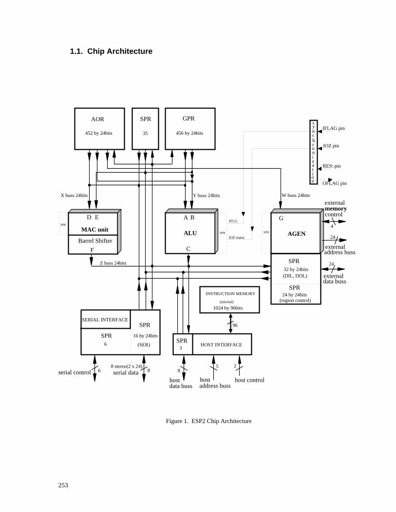
1.1. Chip Architecture
AOR
452 by 24bits
GPR
456 by 24bits
ALU
Z buss 24bits
W buss 24bitsX buss 24bits Y buss 24bits
C
BA
MAC unit
Barrel Shifter
D E
F externaladdress buss
externaldata buss
24
AGEN
(DIL, DOL)
SPR
G
(region control)
SPR
SPR
24
SPR
Figure 1. ESP2 Chip Architecture
IFLG
IOZ status
4
synchronization
IFLAG pin
IOZ pin
RES\ pin
SPR
35
SPR
96
hostaddress buss
host control
SPR3
HOST INTERFACE
hostdata buss
85
32 by 24bits
24 by 24bitsINSTRUCTION MEMORY
1024 by 96bits(internal)
memoryexternal
control
(SER)
serial data8 stereo(2 x 24)
SPR
serial control 6
SPR
SERIAL INTERFACE
16 by 24bits
6
82
OFLAG pin
253

1.1.1. Function Units: MAC, ALU, AGEN The three main function units are designed to execute in parallel employing an instruction set which supports the parallelism. The internal pipeline design dictates a specific hardware ordering-in-time which sees the MAC unit first, followed mid-cycle by the ALU. The AGEN timing exactly parallels that of the MAC unit. Some of the inter-unit pipeline latencies discussed (see the Instruction Cycle Timing diagram), will be more easily understood if this ordering-in-time is kept in mind. The order of each instruction field, on the programmer's single line of code (one instruction cycle, one program line, one instruction line), within which each unit's instruction will be found is: MAC unit ALU AGEN The latencies are few, while easy-to-understand charts are presented in the Software Specification to assist the programmer. It is important that the programmer recognize that the speed and efficiency of the ESP2 processor for most all DSP tasks is facilitated by this pipeline design. One benefit of the parallelism is that the programmer will find many common instructions amoung the units; e.g., both the MAC unit and ALU have identical MOV and identical shift (ASH) syntax, so the programmer can simply cut and paste into the appropriate field. The MAC unit is a three operand device (two source, one destination), plus a seed source. The MAC unit instruction set comprises 20 fundamental instructions, 10 variations, and an assortment of pseudo instructions providing a large palette of multiply/accumulate/shift operations. A prominent feature of the MAC unit is the ability to selectively inhibit latching of the accumulator result while sending it to some destination register. A Barrel Shifter is integral to the MAC unit, available on a per-instruction basis, and can be accessed by the ALU. The Barrel Shifter can be used to shift either the input to the accumulator or the accumulator output. The ALU instruction set consists of 32 standard, non-standard, and Boolean instructions. All of these instructions can take two source operands and another destination operand. The non-standard operations are used for such things as FFTs, envelope generators, stereo-to-mono signal conversion, etc. The ALU instruction set is augmented with a wide assortment of pseudo instructions. Program control instructions which allow conditional branching are found in the ALU. While branching allows the programmer to jump over parallel instructions to the ALU, MAC unit, and AGEN, a separate mechanism allows conditional execution of individual instructions to any or all of the three function units. The AGEN performs modulo addressing of 8 distinct regions of data located nearly anywhere in external physical memory and of any size. Within each region can be defined numerous delaylines whose region address offsets are determined by the multiplicity of AORs employed by AGEN. AGEN features include a Plus-One addressing mode, and UPDATE of the region BASE under program control. The AGEN can also perform absolute addressing as would be required for peripheral I/O.
1.1.2. Internal Registers. Operand addresses are 10 bits allowing up to a total of 1024 internal registers. This register space is apportioned as follows:
Table 1. Internal Register Address Map $000 - $1c7 General Purpose Registers (GPRs) $1c8 - $1ff Special Purpose Registers (SPRs) $200 - $3c3 Address Offset Register (AORs) $3c4 - $3ff Special Purpose Register (SPRs) The ESP2 instruction set operates directly on these registers given meaningful names by the programmer. The MAC unit (with one restriction) and ALU can utilize all the registers as operands.
254

1.1.3. GPR and AOR GPRs (General Purpose Registers) and AORs (Address Offset Registers) are 24-bit wide registers implemented as large dynamic ram arrays. GPRs and AORs have two read ports and one write port. Each of the ports is accessed twice per instruction cycle. This gives a virtual set of four read ports and two write ports per instruction cycle for each of the arrays. The GPR read ports allow two operand fetches for the ALU and two for the MAC unit in an instruction cycle. The two GPR write ports allow one result-write by the ALU and one by the MAC unit. The AOR array is used to hold address offsets for the AGEN. When not used for holding address offsets, AORs may be used just like GPRs. The four AOR read ports allow one offset fetch for the AGEN, one operand fetch for the MAC unit, and two operand fetches for the ALU. The two write ports of the AOR allow one result-write by the ALU and one by the MAC unit. Host access to GPR and AOR is governed by the ALU. Because these registers are dynamic RAM they must be refreshed to maintain the data. The mechanism for refreshing these registers is somewhat transparent and built into the instruction set. GPR and AOR power-up in their lower power state; i.e., when these registers read as logical 1, they are in their lower power consumption state. The address map allows 456 GPRs and 452 AORs. Due to die size limitations, it is not at first planned to include all of these registers. The initial revisions will have 256 GPRs and 256 AORs.
1.1.4. SPR SPRs (Special Purpose Registers) are static registers for holding data specific to a particular operation of a function unit, for interfacing to the external ports of the chip, for controlling certain operating modes, or for chip hardware configuration and status. Internal chip control and status registers, such as the Program Counter (PC) or the Condition Code Register (CCR), are mapped as SPRs to provide access via the system host. Host access to SPR is governed by the ALU. All the function units (ALU, AGEN, MAC) have supporting SPRs. In some instances, one or several SPRs effectively behave as extra source/destination operands to a particular function unit. Unless stated otherwise, these extra source/destination SPRs are subject to the same inter-unit latencies as any conventional source/destination register. (See the section on Inter-Unit Latency.) SPRs are accessible as operands in all of the same modes as GPRs, although some of the SPRs are read-only. SPRs are distributed over the GPR and AOR address space so as to balance the number of GPRs against the number of AORs.
255

1.1.5. Internal Register Usage The rules governing the use of the three types of registers as operands for the three function units are indicated in Table 2. (The symbol * in Table 2 denotes a valid usage.) Notice that an AOR is not a valid E source operand in the MAC unit because one of the AOR's four virtual read ports is usurped by AGEN.
Table 2. Registers as Operands
ALU MAC unit AGEN GPR AOR SPR Buss Source Destination
A * * * X *
B * * * Y *
C * * * Z *
D * * * X *
E * * Y *
F * * * Z *
G * W *
1.1.6. Instruction Memory
The instruction memory is presently a 300 by 96-bit dynamic memory array. These 300 ESP2 instructions are equivalent to 900 instructions of a more conventional architecture because of the three parallel function units that constitute the ESP2. Future expansion sets the maximum possible number of ESP2 instructions at 1024 (3072 conventional). At a sample rate of 44.1 kHz and using a system clock of 40 MHz, ESP2 can execute 226 instruction cycles (678 conventional) per sample period. The instruction memory cell has one write port and one read port and cycles at twice the instruction rate. This allows one cycle for instruction fetching, and a read/write cycle for refresh or host access to the instruction memory array. Refresh of instructions is transparent to the programmer. Instruction memory powers-up in its lower power state; i.e., when instruction memory reads as logical 1, it is in its lower power consumption state. Instruction memory can be downloaded, overlaid, or uploaded by the system host at any time at the instruction rate. This is because the host interface is dichotomized between internal register and instruction memory.
1.1.7. Future Expandability It should be possible to shrink the chip to denser process geometries. This would improve performance by allowing operation at higher clock rates. Since the chip is designed with a 10-bit Program Counter and 10-bit operand (address) fields, we can add GPR, AOR, and instruction memory with minimal layout effort.
1.1.8. Internal Operand Busses
The ESP2 contains four 24-bit data busses, W, X, Y, Z. The X and Y busses are time-multiplexed for fetching ALU and MAC unit source operands. These busses connect to the GPR memory array, the AOR memory array, the ALU, the MAC unit, and to all SPRs. The source register (GPR, AOR, or SPR) specified as the ALU's A operand is always fetched on the X buss, as is the MAC unit's D source operand. The register (GPR, AOR, or SPR) specified as the ALU's B source operand is fetched on the Y buss. The register (GPR or SPR, but no AOR) specified as the MAC unit's E source operand is fetched on the Y buss as well. The AOR addressed as the AGEN's G source operand is fetched on the W buss. The Z buss is used to deliver results to the registers (GPR, AOR, or SPR) designated by destination operands, C and F, from the outputs of the ALU and the MAC unit respectively. The MAC unit and ALU share the X, Y, and Z busses by relinquishing their use on different phases of the same instruction cycle. Instruction Cycle Timing is covered in the section of the same name.
256

1.1.9. External Interfaces There are four mechanisms for interfacing to external memory and devices: the external memory interface, the serial interface, the host interface, and chip synchronization. The external memory interface is a 24-bit address, 24-bit data buss for random access of delaylines and tables stored in external memory. This external memory buss can also be used to access memory-mapped I/O devices. Addresses for this buss are calculated on every instruction cycle by the AGEN, under program control. The code which drives AGEN can be generated automatically for the programmer by the assembler, if desired. The DIL (Data Input Latch) and DOL (Data Output Latch) SPRs provide the interface to the external memory data buss for incoming and outgoing data as they are accessed as normal sources and destinations of instructions, under program control. The external memory buss cycles at the instruction rate. The serial interface consists of 8 serial stereo data lines. Each of the lines can be configured as input or output. There are two fully programmable sets of clocks for controlling the timing of data transfers on the serial data lines, and each data line can be assigned to either set of clocks. The serial clocks may be disabled to allow exogenous devices to dictate the serial timing. The SER data SPRs (e.g., SER0L) provide the interface to incoming and outgoing serial audio data as they are accessed as normal sources and destinations of instructions, under program control. The asynchronous host interface offers an 8-bit data exchange on the host side, but 24-bit on the ESP2 internal register side. It is described more fully in the later section, Host/ESP2 Interface. The host/ESP2-register interface timing internally parallels that of the ALU; the system host transfers data to/from GPR/AOR/SPR registers using normal ALU data paths (the Y and Z busses). Transfers are completely under ESP2 program control, however, the exact time of the register transfer governed by the ALU HOST and BIOZ instructions. The host will not hang waiting for an acknowledge because built-in semaphores are polled by the host. When the chip is halted, it continually executes HOST instructions by design. Instruction memory is always accessible to the system host at the instruction rate regardless of the state of the chip. Instruction memory access does not usurp internal chip resources because there is a dedicated 96-bit buss for this purpose (8 bits wide on the host side). The chip synchronization interface includes the IOZ input pin, the IFLAG input pin, the OFLAG output pin, and the RES\ (reset) pin: The IOZ input pin is most often tied to the system sample rate signal called LRCLK. This signal is asynchronous and comes from any desired source including the ESP2 chip itself. The IOZ pin is indirectly monitored by the ALU BIOZ instruction to synchronize the running ESP2 program to the sample rate. The IFLAG input pin is uncommitted and can be used for any desired purpose. Its intended purpose is for use as a semaphore in a rapid-transfer DMA scheme. It is visible through the CCR in the ALU as IFLG. Other transfer schemes to external memory are discussed in the Applications section. The OFLAG output pin is also uncommitted and can be used for any desired purpose. It is connected to the OFLG bit in the HARD_CONF SPR. The RES\ pin impact is discussed in the Chip Reset and Initialization section. It can be used in a multi-processor environment to initially synchronize several ESP2 chips running in parallel. (Provision has been made in the external memory interface for sharing external memory.)
257

1.2. Instruction Cycle Timing
MAC unit
ALU
AGEN
external
X/Y
Z buss
n-1sources
1 2 3 4 1 1 12 23 34 4
inst n-1
inst n-1
inst n-1
inst n-1
inst n
inst n
inst n
inst n
inst n+1
inst n+1
inst n+1
inst n-2
MACn-1ALU
ALU
ALU
ALU
ALU
ALU ALU
MAC MAC MAC
MACMACMACn-1 n-1
n n
n n
n+1 n+1
n+1 n+1
n+2
n-2dest. dest. dest. dest. dest. dest. dest.
W buss
2
n-1AOR
AGENn n+1 n+2
AGEN AGEN AGEN
memory
busses
DIL/DOLn-2
DOLn-2DIL
n-1DOL
nDOL
n+1DOL
n-1DIL DIL
n
sources sources sources sources sources sources
n-1sources
AGENn n+1 n+2
AGEN AGEN
sources sources
AGEN
sources
n-1
BASEUPDATE
n
BASEUPDATE
n+1
BASEUPDATEcontrol registers
(extra sources = SIZEM1, BASE, END)
access
Tstate
AOR AOR AOR
region
source source source sourcedest. dest. dest.
n n+2n+1PC value n-1
AGEN SPRs
Figure 2. Instruction Cycle Timing diagram
258
All ESP2 instructions execute in one instruction cycle. The Instruction Cycle Timing diagram shown in Figure 2 illustrates the relative timing of instruction execution for each of the function units (MAC, ALU, AGEN), and their timing relationship with the access to external memory. Notice that the external memory access lags the AGEN instruction requesting it. The access to internal source/destination operands is also indicated. Execution timing in the MAC unit and ALU are interleaved to allow four operand-fetches and two operand-stores by multiplexing the X, Y, and Z busses. By operating these busses at twice the instruction rate, the MAC unit and ALU can each be supplied with two source operands from GPR/AOR/SPRs and have their results stored back into GPR/AOR/SPRs on every instruction cycle.
1.3. Latency
There are five categories of execution latency due to the internal pipeline architecture: 1)inter-unit, 2)external memory access, 3)ALU instruction cycle execution, and 4)serial data access, 5)pointer register access for indirect register addressing. The last three categories are discussed in the pertinent sections. With few exceptions, when latencies arise, the latency across the categories is one instruction cycle. This regularity makes for a highly orthogonal design.
1.3.1. Inter-Unit Latency The interleaving of the MAC unit and ALU timing produces some latency in the availability of the result of the ALU instruction with respect to the MAC unit instruction. As illustrated in Figure 2, the MAC unit fetches its source operands for the (n+1)th queued instruction before the ALU has stored operation results to its destination from the nth instruction. Similar latencies arise between the AGEN and the ALU since the AGEN fetches are coincident with those of the MAC unit. The AGEN source operands (which include the AOR (address offset), and BASE, SIZEM1, and END region control registers) are acquired at the beginning of an instruction cycle, while there is an optional UPDATE of the region BASE at the end of the cycle.
1.3.2. Latency of External Memory Access via AGEN AGEN must calculate an address during one instruction cycle while the external memory access at that address physically takes place during the next instruction cycle. The external memory data-interface registers, the SPRs called DILs and DOLs, look like any other register to the MAC unit and ALU. In the case of external memory reads (RD), this pipeline design requires the assembler to schedule a RD at least two instruction cycles before the data is actually supplied to the ALU or MAC unit via DIL (Data Input Latch). In the case of external memory writes (WR), the pipeline delays the usage of the MAC unit and ALU results written out via DOL (Data Output Latch). The pipeline design allows a WR from the MAC unit to external memory to be scheduled as early as the same instruction cycle as the MAC unit instruction which requested it (or any time thereafter). But the pipeline design allows a WR from the ALU to be scheduled no sooner than one instruction cycle after the requesting ALU instruction.
259

The following manifest quantifies the inter-unit latencies and the AGEN scheduling rules: The interleaving of the MAC unit and ALU operations and the alignment of the AGEN timing with the MAC unit timing have important ramifications from a programming point of view. The following rules summarize the register data access latencies between function units. Nonlatent operations 1. The result of a MAC unit operation is available for use as a source operand by the MAC unit
no sooner than the next instruction cycle (next queued program line). 2. The result of a MAC unit operation is available for use as a source operand by the ALU no
sooner than the next instruction cycle. 3. The result of an ALU operation is available for use as a source operand by the ALU no sooner
than the next instruction cycle. 4. The result of a MAC unit operation written to an AOR or AGEN region control register is
available to the AGEN no sooner than the next instruction cycle. Latent operations 5. The result of an ALU operation is available for use as a source operand by the MAC unit
no sooner than the second instruction cycle following the ALU instruction. 6. The result of an ALU operation written to an AOR or AGEN region control register is
available to the AGEN no sooner than the second instruction cycle following the ALU instruction. The scheduling of DIL/DOL RD/WR from/to external memory, relative to the timing of MAC unit and ALU operand access, follows these rules: Alatent operation 7. External memory writes of MAC unit results to DOL can be scheduled on the same program
line (or on any line thereafter) as the instruction which generates the data. Nonlatent operation 8. External memory writes of ALU results to DOL can be scheduled no sooner than one
instruction cycle after the instruction which generates the data. Latent operation 9. The fetch of data from external memory for use by either the ALU or the MAC unit as a DIL
source operand must be scheduled at least two instruction cycles prior to the sourcing instruction. For a nice programmer's chart, see the ESP2 Language and Software Specification in the Pipeline section.
260

2. Multiplier/Accumulator/Shifter
2.1. Architecture
24 X 24 bit Multiplier
52 bit Accumulator
MAC latchMAC Preload latch
4 to 1 MUX
60 bit left/right Barrel Shift
Overflow Detect Logic
output to Z buss
X buss Y buss
Z buss
X or Y busses
MACZERO
MAC Result Low latch
X or Y busses
49 (sign extended to 52)
52 LSB
48 LSB
52
52
60
24 MSB
48 LSB
24 LSB
left shift 1
48
52
52 (sign extended to 60)
D E
(MACP) (MAC)
(MACRL)
available as input from
F operand
2 x 24loadable via
available as input from
(MACZ)
(2 x 24)
Figure 3. MAC unit architecture. Bold buss shows first half instruction cycle.
261
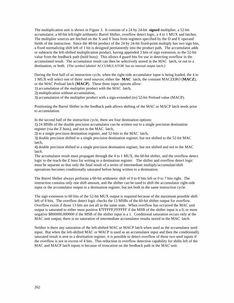
The multiplication unit is shown in Figure 3. It consists of a 24 by 24-bit signed multiplier, a 52-bit accumulator, a 60-bit left/right arithmetic Barrel Shifter, overflow detect logic, a 4 to 1 MUX and latches. The multiplier sources are fetched on the X and Y buss from registers specified by the D and E operand fields of the instruction. Since the 48-bit product of the 24 by 24-bit fixed-point multiply has two sign bits, a fixed normalizing shift left of 1 bit is designed permanently into the product path. The accumulator adds or subtracts the left-shifted multiplication product, having appended 3 bits of sign extension, to the 52-bit value from the feedback path (bold buss). This allows 4 guard bits for use in detecting overflow in the accumulated result. The accumulator result can then be selectively stored in the MAC latch, or out to a destination, or both. (The symbol labeled 'ACCUMULATOR' has no internal output latch.) During the first half of an instruction cycle, when the right-side accumulator input is being loaded, the 4 to 1 MUX will select one of three seed sources; either the MAC latch, the constant MACZERO (MACZ), or the MAC Preload latch (MACP). These three input options allow: 1) accumulation of the multiplier product with the MAC latch, 2) multiplication without accumulation, 3) accumulation of the multiplier product with a sign-extended (to) 52-bit Preload value (MACP). Positioning the Barrel Shifter in the feedback path allows shifting of the MAC or MACP latch seeds prior to accumulation. In the second half of the instruction cycle, there are four destination options: 1) 24 MSBs of the double precision accumulator can be written out to a single precision destination register (via the Z buss), and not to the MAC latch, 2) to a single precision destination register, and 52-bits to the MAC latch, 3) double precision shifted to a single precision destination register, but not shifted to the 52-bit MAC latch, 4) double precision shifted to a single precision destination register, but not shifted and not to the MAC latch. The accumulator result must propagate through the 4 to 1 MUX, the 60-bit shifter, and the overflow detect logic to the reach the Z buss for writing to a destination register. The shifter and overflow detect logic must be separate so that only the final result of a series of intermediate multiply/accumulate/shift operations becomes conditionally saturated before being written to a destination. The Barrel Shifter always performs a 60-bit arithmetic shift of 0 to 8 bits left or 0 to 7 bits right. The instruction contains only one shift amount, and the shifter can be used to shift the accumulator right-side input or the accumulator output to a destination register, but not both in the same instruction cycle. The sign extension to 60 bits of the 52-bit MUX output is required because of the maximum possible shift left of 8 bits. The overflow detect logic checks the 13 MSBs of the 60-bit shifter output for overflow. Overflow exists if those 13 bits are not all in the same state. When overflow has occurred the MAC unit output is saturated to either most positive $7FFFFF,FFFFFF if the MSB of the shifter input is a 0, or most negative $800000,000000 if the MSB of the shifter input is a 1. Conditional saturation occurs only at the MAC unit output; there is no saturation of intermediate accumulator results stored in the MAC latch. Neither is there any saturation of the left-shifted MAC or MACP latch when used as the accumulator seed input. But when the left-shifted MAC or MACP is used as an accumulator input and then the conditionally saturated result is sent to a destination register, it is possible to detect overflow of these two seed inputs if the overflow is not in excess of 4 bits. This reduction in overflow detection capability for shifts left of the MAC and MACP latch inputs is because of truncation on the feedback path in the MAC unit.
262

2.1.1. Exception Processing There are two special cases that must be handled by the MAC unit:
Table 3. Multiplier Exceptions
MAC latch Destination: F,MACRL $800000 X $800000 = $0,800000,000000 = $7FFFFF,FFFFFF -$800000 X $800000 = $f,800000,000000 = $800000,000000
2.2. MAC unit Barrel Shifter The Barrel Shifter residing within the MAC unit performs only arithmetic shifts. The Barrel Shifter performs two functions: 1) It can be used on the accumulator output path to perform a shift of +8 (left) to -7 bits of the 52-bit accumulated sign-extended (to 60 bit) result. 2) The Barrel Shifter can be applied to the MAC latch as seed-source, or to Preload values in the MACP latch as seed-source, for double precision shifting by +8 to -7 bits. If it is desired to examine the 4 MAC latch guard bits, this can be done by first right-shifting them in place back into the MAC latch. They can then be examined by sourcing directly from the MAC latch (the SPR MACH). ASSEMBLER NOTE: The shift code stored in the instruction is an unsigned 4-bit value. The value is derived by the following equation: Shift code = desired shift amount + 7 Since the desired shift amount is in the range from +8 to -7 bits, the result of the Shift code equation falls into the range 0 to 15.
2.3. Accessing the MAC unit The MACP latch is accessible as two pairs of 24-bit write-only SPRs: MACP_H and MACP_L, and MACP_HC and MACP_LS. The ESP2 assembler generally disallows any reference to MACP as a source operand which is not the seed source in the MAC unit. When MACP is used as a single precision destination, this is synonymous with the SPR, MACP_HC. The unsaturated MAC latch is directly accessible as a pair of 24-bit read-only SPRs, MACH and MACL, for use as source operands in the ALU or MAC unit with normal latencies. From the ALU, using the MAC latch as a destination is disallowed by the assembler. When MAC is used as a single precision source operand, this is synonymous with the SPR, MACH.
263

2.3.1. Writing the MACP (Preload) latch MACP is used in accumulation, instead of the MAC latch or MACZ, under control of the program. The MACP latch is nonvolatile and will retain a value written to it until written again. Because of the interrelationship between the ALU and MAC unit instruction timing, the value written by the ALU into the high or low-order bits of MACP during the nth instruction line will be available for accumulation 2 instruction cycles later at the (n + 2)th queued instruction line. The MAC unit can also initialize the high or low-order MACP latch, just as it can load any other SPR. In this case, MACP is available to the MAC unit on the next instruction cycle. The ALU and the MAC unit can be used in conjunction to initialize the full 52 (high and low-order) bits of the MACP latch.
When the SPRs, MACP_H or MACP_L, are written, the 24-bit value is written into the indicated half of the MACP latch. When the SPR, MACP_HC, is written, 24 bits are written into the high-order half of the MACP latch while the low-order half is cleared to all zeros. When SPR, MACP_LS, is written, the 24-bit value is written into the low-order half of MACP while the high-order half is written with the sign-extension of the value in the low-order half. These allow MACP initialization to the full 52-bit accumulator width in one instruction cycle. Any write to the high-order half of the MACP latch is sign-extended into the 4 guard bits to create a full 52-bit word.
2.3.2. Reading the MAC latch Since the MAC latch is located before the overflow detect in the circuit topology, values read from the MAC latch (using the MAC unit SPRs, MACH and MACL, as sources) will not be conditionally saturated. Our intention was to provide unsaturated MAC unit results as source operand for the MAC unit itself as well as for the ALU. Also note from observation of the fundamental instructions, that the MAC latch will be unshifted with regard to the last executed MAC unit instruction if it was not of the form: MAC(P) >>n +/- D X E > MAC(,F) That is to say for many instructions, the MAC unit output is shifted but the MAC latch acting as extra destination is not.
2.3.3. MAC Result Low latch (MACRL)
Examination of the fundamental MAC unit instructions shows that the MAC unit has a destination on every instruction cycle. If the programmer does not specify one, the assembler chooses the read-only ZERO SPR as the destination. On every instruction cycle, the low 24 bits of the conditionally saturated MAC unit output will be written to the MAC Result Low latch because it is in the output path. Since MACRL is mapped as an SPR, it is readable by the MAC unit and ALU as a source operand. Storing the low word allows double precision arithmetic using all 48 bits of the final result out of the MAC unit. It is necessary to read the MAC Result Low latch before it is overwritten by the MAC unit in the next instruction cycle. The only exception is when the MAC unit is executing NOPs in which case the contents of MACRL will be preserved (see the MAC unit NOP pseudo instruction).
264

2.4. MAC unit Instructions The fundamental instructions executed by the MAC unit are two-source one-destination instructions, having an optional seed source and an optional MAC latch destination, of the form: (MAC(P)) +/- D X E > (MAC,)F When a seed source is not specified, the assembler inserts MACZERO (MACZ). The D and F operands can be any GPR, SPR, or AOR. The E operand can be any GPR or SPR. The F operand acts as the register-type destination. At least one of the two destinations must be specified by the programmer. When the only destination specified is MAC, the assembler substitutes the read-only SPR called ZERO for the F operand. Unsaturated results of the accumulation are stored in the MAC latch (the SPRs: MACH, MACL) for use in subsequent accumulations. When the only destination specified is F, the MAC latch is inhibited as a destination. This inhibition is a means to preserve the previous MAC latch contents. Table 4 lists the fundamental instructions of the MAC function unit: (Parenthesis not required; it only serves to clarify the operation.)
Table 4. MAC unit List of Instructions MACZERO + D X E > MAC >>n MACZERO - D X E > MAC >>n MACZERO + D X E >>n MACZERO - D X E >>n
> F > F > F > F
MAC + D X E > MAC >>n MAC - D X E > MAC >>n (MAC + D X E) >>n (MAC - D X E) >>n
> F > F > F > F
MAC >>n + D X E MAC >>n - D X E MAC >>n + D X E MAC >>n - D X E
> MAC, F > MAC, F > F > F
MACP + D X E > MAC >>n MACP - D X E > MAC >>n (MACP + D X E) >>n (MACP - D X E) >>n
> F > F > F > F
MACP >>n + D X E MACP >>n - D X E MACP >>n + D X E MACP >>n - D X E
> MAC, F > MAC, F > F > F
In six of the instructions in Table 4, notice the MAC latch gets the unshifted unsaturated result while the destination operand, F, gets the shifted and conditionally saturated result. In four other cases, the MAC or MACP latch as seed source is shifted, but the MAC latch as extra destination remains unsaturated. But in all cases, the destination, F, receives the shifted and conditionally saturated result. The shift amount n, as specified in Table 4, can be +7 to -8 bits; specified as <<n it can be -7 to +8 bits. The shift amount n is a constant expression that is encoded into the micro-instruction word.
265

2.5. MAC unit Pseudo Instructions The MAC unit pseudo instructions are designed to preserve the MAC latch where possible. Therefore most pseudos do not provide MAC as a destination. Note that the MAC latch is neither a valid destination from the ALU (but MACP is). Generally speaking, only the MAC unit pseudo, NOP, preserves MACRL. ADD D, MAC > MAC, F = MAC - D X MINUS1 > MAC, F ! destination is MAC or F or both
ADD D, MAC > MAC >>n > F = MAC - D X MINUS1 > MAC >>n > F
ADD D, MAC = MAC - D X MINUS1 > MAC
ADD D, MAC >>n > MAC = MAC >>n - D X MINUS1 > MAC
ADD D, MACP > MAC, F = MACP - D X MINUS1 > MAC, F ! destination is MAC or F or both
ADD D, MACP > MAC >>n > F = MACP - D X MINUS1 > MAC >>n > F
ADD D, MACP = MACP - D X MINUS1 > MACP
ADD D, MACP >>n > MAC = MACP >>n - D X MINUS1 > MAC The MAC latch as a destination is unsaturated, double precision. MACP as destination is single precision, conditionally saturated. ASH D >>n > F = - D X MINUS1 >>n > F
ASH some_reg >>n = - some_reg X MINUS1 >>n > some_reg This pseudo instruction performs an arithmetic shift n places of the 24 bit D operand. The value n which is encoded in the micro-instruction is the shift range; it is a constant expression which can take any value in the range +7 to -8 bits. ASH D >>8 > F = D X HALF >>7 > F
ASH some_reg >>8 = some_reg X HALF >>7 > some_reg These two extra pseudo instruction definitions make the range of shift for ASH symmetrical. Alternatively the programmer might choose the constant (HALF, MINUS1) to be smaller (using the primitive instruction) thus extending the range of possible shifts right even further. In a shift right, the programmer should be aware that the MACRL SPR receives all of the bits shifted out of the single precision D operand. This means that bits of the single precision operand are not lost when shifted across the LSB boundary. Considering these pseudo instruction definitions, the 48-bit concatenation, (some_reg,MACRL), will contain all 24 of the right-shifted bits of some_reg. PROGRAMMER NOTE: Double precision SHIFTMAC(P) pseudos or the ALU's double precision shift instructions should also be considered. Note that the ALU's ASH pseudo instruction can not incorporate the MACRL SPR to catch the LSBs as explained here for the MAC unit. CLR F = MACZ + ZERO X ZERO > F
266
DBL D > F = - D X MINUS1 <<1 > F
DBL some_reg = - some_reg X MINUS1 <<1 > some_reg
EXIT = MACZ + ZERO X ZERO > REPT_CNT This MAC unit pseudo instruction is used to terminate a repeating block of code, instigated by the REPT instruction, at the end of the current block. The MAC unit EXIT pseudo instruction may be placed anywhere within a repeated instruction block except for the last line of the block where it will not work at all. See the description of the ALU REPT instruction and the section on SPR Hazards for more details. HALVE D > F = - D X MINUS1 >>1 > F
HALVE some_reg = - some_reg X MINUS1 >>1 > some_reg MOV D > F = - D X MINUS1 > F This allows the multiplier to do a MOV from operand D to operand F. If the D operand is MAC, then the destination will receive the unsaturated MAC latch (MACH) from the previous queued MAC unit operation. This pseudo instruction does not preserve MACRL. PROGRAMMER NOTE: This instruction uses the MINUS1 SPR ($800000) as the E operand. MOV to the MAC latch is discouraged because the MACP latch fulfills any role as preload register, and because the MAC latch is not a valid destination from the ALU. MOVSMAC > F = MAC + ZERO X ZERO > F
MOVSMACP > F = MACP + ZERO X ZERO > F These pseudo instructions send the double precision conditionally saturated MAC or MACP latch to the single precision destination. If you wish to move the unsaturated MAC latch to a destination, use the MOV pseudo instruction above or the ALU MOV instruction. NEG D > F = D X MINUS1 > F
NEG some_reg = some_reg X MINUS1 > some_reg
267

NOP = MACRL X ONE >>1 > ZERO This NOP for the MAC unit, utilizing the SPR called ONE, preserves MACRL. Since the least significant 24-bits of the MAC unit result are always stored in MACRL, this instruction performs a move of the MACRL SPR to itself. The MAC latch is not written, hence it is preserved. This instruction performs no refresh. NORFSH Identical to NOP RFSH = - REF X MINUS1 > REF This instruction performs a MOV using the REF SPR as source and destination registers. See the section on GPR and AOR Refresh for details on this SPR and its use in refreshing internal DRAM. Execution of this instruction will cause the loss of the contents of MACRL from the previous queued MAC unit instruction. SHIFTMAC >>n = MAC >>n + ZERO X ZERO > MAC
SHIFTMAC >>n > MAC = MAC >>n + ZERO X ZERO > MAC
SHIFTMAC >>n > F = MAC + ZERO X ZERO >>n > F
SHIFTMACP >>n > MAC = MACP >>n + ZERO X ZERO > MAC
SHIFTMACP >>n > F = MACP + ZERO X ZERO >>n > F The SHIFTMAC and SHIFTMACP pseudo instructions perform an arithmetic shift of the 52 bit MAC latch and MAC Preload latch contents, respectively. The constant expression, n, in the equation is the shift amount; it can take any value in the range -8 to +7 bits. If MAC appears as a destination, it remains unsaturated, but it is shifted with double precision. Unlike the MAC latch, the double precision MACP cannot be shifted in place, which explains why there is no corresponding simplest form of SHIFTMACP. As always, any result written to a destination register (including MACP) is single precision and conditionally saturated. PROGRAMMER NOTE: The rationale behind the definition of these pseudos is the following: First, we want double precision results unless a single precision destination register is specified. Second, consider the construct, MAC >>n or MACP >>n + ZERO X ZERO > MAC,F F is conditionally saturated but not guaranteed saturated correctly in a shift left because the MAC unit feedback path is truncated. Therefore, we can only use this construct reliably for SHIFTMAC(P) when the only destination is MAC (F is the ZERO SPR), because the MAC latch is never saturated.
268
SQR some_reg > F = some_reg X some_reg > F
SQR some_reg = some_reg X some_reg > some_reg This is a short hand way of multiplying a number by itself. ASSEMBLER NOTE: AORs cannot be squared because the MAC unit can only get one source operand from AORs. This event should be flagged as an error for the user. SUB D, MAC > MAC, F = MAC + D X MINUS1 > MAC, F ! destination is MAC or F or both
SUB D, MAC > MAC >>n > F = MAC + D X MINUS1 > MAC >>n > F
SUB D, MAC = MAC + D X MINUS1 > MAC
SUB D, MAC >>n > MAC = MAC >>n + D X MINUS1 > MAC
SUB D, MACP > MAC, F = MACP + D X MINUS1 > MAC, F ! destination is MAC or F or both
SUB D, MACP > MAC >>n > F = MACP + D X MINUS1 > MAC >>n > F
SUB D, MACP = MACP + D X MINUS1 > MACP
SUB D, MACP >>n > MAC = MACP >>n + D X MINUS1 > MAC The MAC latch as a destination is unsaturated, double precision. MACP as destination is single precision, conditionally saturated. XCH some_reg1, some_reg2 = - some_reg1 X MINUS1 > some_reg2 MOV some_reg2 > some_reg1 The exchange instruction is a macro-pseudo instruction which uses one MAC unit operation and one ALU operation in order to exchange the contents of two registers. During an XCH instruction, the MAC unit executes a MOV (pseudo) instruction as defined above, while the ALU also executes a MOV instruction but in the opposite direction. Since the operation of the MAC unit and ALU is interleaved, the register contents are swapped using fewer instructions than either function unit acting alone would require. The complete results are discernible to the ALU on the next instruction cycle, but due to inter-unit latency, only some_reg2 is discernible to the MAC unit on the instruction cycle following the exchange; there, some_reg1 still holds its original contents. On the second instruction cycle following the exchange, the complete results are discernible to the MAC unit. ASSEMBLER NOTE: An XCH specified in the MAC unit instruction field employs both the MAC unit and the ALU, therefore no ALU operation can be specified on that instruction line. A warning should be issued if indirection is specified because to work properly, the programmer must have set up the INDIRB and/or INDIRC SPRs in the ALU, while it is the INDIRD and/or INDIRF (not INDIRE) SPRs which must have been set up in the MAC unit.
269

3. ALU and Instruction Set The Arithmetic Logic unit can perform a variety of general and special purpose arithmetic, data movement, and logical operations. It incorporates classical zero-overhead saturation arithmetic for handling computational overflow, and can shift double precision signals to the left or right for the purpose of normalization. Instructions exist to perform unsigned arithmetic without saturation. During every instruction cycle the ALU takes one or two 24-bit source operands and produces a 24-bit result which is sent to a (third) destination register. ALU execution overlaps with the operation of the MAC unit, so the two computation units operate in parallel. Detailed description of the ALU and MAC unit execution cycles may be found in the section on Instruction Cycle Timing. The instructions executed by the ALU are three-operand instructions of the form:
OPERATION A, B > C The source A and B operands can be any GPR or SPR or AOR. The C operand is the destination and it can also be any internal register. Since external memory access takes place via the interface SPRs called DIL and DOL, the available operands virtually include external memory data. Some of the instructions that follow (especially program control instructions) do not use all of the three available operands. Some of the instructions store data in the operand (address) fields themselves. Directions have been included showing how the assembler should regard the operands and operand fields of those instructions. The mnemonic ZERO, used often as an operand, refers to the read-only SPR whose content is zero.
270

3.1. ALU Instructions These are the fundamental instructions of the ALU: ADD is a saturating 2's complement addition operator used to create the sum of two signals. If
the sum cannot be represented in 24 bits, full-scale positive ($7FFFFF) or full-scale negative ($800000) is substituted for the overflowed result. The operation performed is:
C = A + B
ADDC Add with carry is a 2's complement saturating addition operator like ADD, but the carry
bit in the Condition Code Register (CCR) is added at the LSB. This is valuable for double precision arithmetic. The operation performed is:
C = A + B + carry
When the ADDC instruction is used in conjunction with a preceding ADDV to perform double precision arithmetic, the ADDC operation can saturate the high 24-bit word of the 48-bit result. Since the low 24-bit word was computed in the preceding ADDV operation, its value will not be conditionally saturated. The low word of the result can be adjusted by the following conditional operation: ADDV a_low, b_low > c_low ADDC a_high, b_high > c_high IF OV XOR MINUS1, c_high > c_low (See the section on ALU Pseudo Instructions for the IF pseudo, and see the section on Setting Condition Codes for information on the V flag.)
PROGRAMMER NOTE: Since conditionally executed instructions never modify the Condition
Code Register, a double precision addition using the ADDC instruction will not execute properly if the preceding ADDV is conditionally executed .
ADDV is an unsaturating addition operator. It operates exactly as ADD, except that it lacks
overflow detection. For this reason it is not normally used to add signals together, unless the signals are double precision. However, it can be used for generating ramp signals, for performing unsigned address arithmetic, and for double precision arithmetic. It performs the operation:
C = A + B
271

AMDF This instruction first subtracts the operands as B - A with conditional saturation, and then takes the (one's complement) absolute value of the result. Equivalent Pseudo-code: if (B - A) < 0 then C = (B - A) ^ $FFFFFF /* exclusive OR */ else C = B - A This implementation employing the exclusive OR operation, instead of negation, yields the absolute value of negative numbers which are off by 1, making the magnitude of the destination smaller by one LSB of a 24-bit word in two's complement. This instruction is typically found in pitch detection applications where this error is insignificant. If the error needs to be corrected however, then the state of the N flag in the CCR can be monitored.
AND performs the bit-wise logical AND of the two 24-bit operands: C = A & B
AS performs an arithmetic shift of B by the contents of A using destination C. Saturation will
occur if any of the bits shifted left through the MSB differ from the original sign bit. The shift amount is restricted to the range of +8 to -8 bits. Positive values correspond to left shifts and negative values correspond to right shifts. Zeros enter the LSB during left shifts and the sign enters the MSB during right shifts. (See the ASH pseudo.)
272

ASDH Arithmetic Shift Double High performs a double precision arithmetic shift using the B operand as the high word and the A operand as the low word of a 48-bit input. Saturation will occur if any of the bits shifted left through the MSB differ from the original sign bit. The shift amount for this operation comes from the ALU_SHIFT SPR and its range is restricted to +8 through -8 bits as in the AS instruction. Zeros enter at the low-word LSB in a left shift, and the sign enters at the high-word MSB in a right shift. The result is the high 24-bit word of the conditionally saturated 48-bit shift output. ASSEMBLER NOTE: Switch the operands on this instruction so that ASDH gpr1,gpr2 gets assembled as gpr2 being the A operand and gpr1 being the B operand. This allows the two halves of a double precision word to appear in proper order. In this particular example, gpr2 is the destination (the C operand). PROGRAMMER NOTE: See the assembler note above. This switch of the operands hobbles indirection. To indirect on gpr1 the programmer must write to INDIRB, and vice-versa. The programmer must always use the verbose form of the instruction explicitly declaring the destination to successfully implement indirection.
ASDL Arithmetic Shift Double Low performs a double precision arithmetic shift using the B
operand as the high word and the A operand as the low word of a 48-bit input. The shift amount for this operation comes from the ALU_SHIFT SPR and its range is restricted to +8 through -8 bits as in the AS instruction. Zeros enter at the low-word LSB in a left shift, and the sign enters at the high-word MSB in a right shift. The result is the low 24-bit word of the 48-bit shift output. The ALU performs this and the ASDH instruction by intelligently extracting a 32-bit field from the 48-bit input based on shift direction and whether the low or high word is the desired result. When the low word is desired, the MSBs of the input are lost before the shift and are, therefore, not available for detecting overflow during a shift. ASSEMBLER NOTE: Switch the operands on this instruction so that ASDL gpr1,gpr2 gets assembled as gpr2 being the A operand and gpr1 being the B operand. This allows the two halves of a double precision word to appear in proper order. In this particular example, gpr2 is the destination (the C operand). PROGRAMMER NOTE: See the assembler note above. This switch of the operands hobbles indirection. To indirect on gpr1 the programmer must write to INDIRB, and vice-versa. The programmer must always use the verbose form of the instruction explicitly declaring the destination to successfully implement indirection.
PROGRAMMER NOTE: The result of this instruction will saturate to $FFFFFF or $000000
when the V flag in the Condition Code Register is true from the previous queued ALU instruction. The direction of overflow will be determined by the N flag of the Condition Code Register from the previous queued ALU instruction. The N and Z flags will then be set based on the 24-bit result from this instruction, the V flag will not be modified.
If the saturation feature is undesirable, use the LSDL instruction instead. PROGRAMMER NOTE: Since conditionally executed instructions never modify the Condition Code Register, a double precision shift using the ASDL instruction will not conditionally saturate reliably based on the previous queued ALU instruction if that previous instruction is conditionally executed .
273

AVG takes the average of two operands: C = (B + A) >>1 The guard bit of the addition result is included in the shift, therefore overflow is not possible.
This means that two full scale signals may be used as inputs without a saturated result. Often used for stereo to monophonic signal conversion. PROGRAMMER NOTE: The operation, (B - A) >>1 , can be coded using the AVG instruction as follows: AVG somereg_a, somereg_b > somereg_c SUB somereg_a, somereg_c > some_other_reg This method stores (B+A) >>1 in somereg_c. This method also avoids the possibility of saturation in the intermediate result that could occur in the more obvious coding that follows: SUB somereg_a, somereg_b > somereg_c AS #-1, somereg_c > some_other_reg
274

BIOZ is a sample-rate synchronization instruction which conditionally sets the BIOZ bit in the HOST_CNTL register. A high BIOZ bit suspends the chip. The BIOZ bit is set when this instruction is encountered and the IOZ status bit of the HOST_CNTL register is found low. The chip will stay in a state of suspension while the IOZ status bit remains low. Execution will resume when the IOZ status bit is set, for then the BIOZ bit will be automatically cleared. If the IOZ status bit is set before the BIOZ instruction is encountered, then the BIOZ bit cannot go high, hence no suspension will occur. The IOZ status bit is automatically set by a low to high transition of the IOZ input pin while the IOZ_EN bit in the HOST_CNTL register is high. The IOZ pin is an asynchronous input which is synchronized to the instruction cycle by the synchronization interface. It is most often tied to the sample rate signal called LRCLK (which is also allowed to be asynchronous with regard to serial data transfer I/O). Taking the IOZ_EN bit low will disable the detection of subsequent IOZ input pin transitions, hence disabling the subsequent setting of the IOZ status bit, and will therefore hold the chip in BIOZ suspension indefinitely (assuming that a BIOZ instruction was encountered in the running program). If IOZ_EN goes low after the IOZ status bit was set, the subsequent BIOZ instruction will observe a high IOZ status bit. Hence, indefinite suspension will occur the next time around. When IOZ_EN is again set high, the next low to high transition on the IOZ pin sets the IOZ status bit. All this can be more easily understood by observing the schematic below:
D R
DR
5V
BIOZ bit
IOZ pin
IOZ_EN
IOZ status bit
BIOZ instr.
Q
Q
D R Q 5V'74 Q
_
Figure 4 The IOZ status bit appears in the CCR, the HOST_CNTL interface register, and in HOST_CNTL_SPR. The BIOZ instruction automatically monitors the bit which appears in the CCR and which is updated on a per instruction basis. Unlike the IFLAG pin, nowhere does an image of the IOZ input pin exist. The system host has read/write access to the IOZ status bit, the IOZ_EN bit, and the BIOZ bit through the HOST_CNTL interface register. In order to allow run-time host access to internal registers, the ALU will execute HOST instructions but only while in suspension; as it does during chip halt (see the section on Halt and Suspension States). The example program and its Equivalent Pseudo-code shows that suspension is not guaranteed by the mere execution of a BIOZ instruction. We see that the instruction cycle corresponding to the BIOZ instruction itself is used to perform one internal register refresh. Keep in mind that all instructions in the example program are executed only once. example program: NOP BIOZ NOP next queued instr. 2nd queued instr.
275

Equivalent Pseudo-code: example program: NOP MOV REF > REF NOP /* BIOZ bit is always clear coming in. */ /* These B and C operands are supplied by the assembler. */ if (IOZ status bit) /* Set on low to high transition of IOZ pin. */ clear IOZ status bit else set BIOZ bit execute next queued instr. /* Execution latency */ if (IOZ status bit) clear BIOZ bit clear IOZ status bit /* Zero it for detection of next sample period. */ while (BIOZ bit) /* Suspension. */ HOST /* Auto refresh or host access. */ /* B and C operands for HOST are supplied by the hardware as REF. */ if (IOZ status bit) /* Set on low to high transition of IOZ pin. */ clear BIOZ bit clear IOZ status bit /* Zero for start of next period. */ execute 2nd queued instr. /* Resume program. */ The BIOZ instruction does not always cause chip suspension. Suspension will not occur when a program main loop equals or exceeds the sample period. BIOZ has an instruction cycle execution latency of 1. If the chip shall enter into a state of suspension then there is a one instruction cycle latency before so. Therefore the instruction line queued for execution following BIOZ (which is
not necessarily the instruction line at PC value + 1 (See the section on Instruction Cycle Execution Latency.) ) will execute before the suspension becomes effective. When suspension terminates, execution resumes with the 2nd instruction line queued for execution following BIOZ. PROGRAMMER NOTE: If the number of instruction lines in every program main loop is precisely equal to the sample period, this means that the BIOZ instruction will never allow host access because the chip never goes into suspension. In this case, the programmer must include HOST instructions elsewhere in the code if host access is desired at run-time. If an occasional program loop exceeds the sample period (which is allowed by the chip synchronization interface), then BIOZ will not allow host access on that particular loop for the same reason. The BIOZ instruction always performs at least one refresh of internal registers as evidenced by the first line of Pseudo-code. When the application program spends time in suspension (in the while-loop inside the BIOZ instruction) more internal registers are refreshed. The HALT_REF_DIS bit in the HARD_CONF SPR must be low during suspension (or halt) for the HOST instruction in the while-loop to perform refresh when no host access is pending. During halt or suspension, the MAC unit can be forced to do refresh, effectively doubling the refresh rate, if the HALT_MAC_REF bit in the HARD_CONF SPR is set. This doubling comes at the expense of the loss of the contents of the MACRL SPR (the low-order MAC unit result from the queued instruction line executed prior to halt or suspension).
ASSEMBLER NOTE: It is critical that BIOZ be used be perform refresh by setting the B and C operands to the SPR called REF for the MOV operation. The A operand is ZERO.
276

BREV performs a classical bit reverse operation on the full 24 bits of the B operand. This instruction is used in a radix-2 FFT and can be used for FFTs of any binary size up to 2**24. The usage in a loop is the same as for DREV. The operation on the bits is as follows:
23 > 0
22 > 1 21 > 2
.
.
. 1 > 22 0 > 23
The BREV instruction can also be used to reverse the order of bits emerging or received from the serial interface data lines; e.g.,
BREV some_reg > SER2L /* instead of MOV */
ASSEMBLER NOTE: The A operand of this instruction is a don't-care. For consistency the ZERO SPR should be used for the A operand.
DREV performs a digit reverse operation on the full 24 bits of the B operand. The operation on
the bits is as follows: 23 > 1 22 > 0
21 > 3 20 > 2
19 > 5 18 > 4 . . . 1 > 23 0 > 22 This instruction is used in a radix-4 FFT of any quaternary size up to 2**24. Example of usage in a loop: ADDV #(2**24)/N, index ! where N = size of FFT DREV index > drev_index ! index = 0 -> N-1 ASSEMBLER NOTE: The A operand of this instruction is a don't-care. For consistency the ZERO SPR should be used for the A operand.
277
HOST provides host access to GPR/SPR/AOR via the host interface registers. The HOST_GPR_PEND bit of the HOST_GPR_CNTL interface register is automatically checked by the ESP2 for a host access request. If an access is pending, one MOV instruction is automatically executed which transfers data between the HOST_GPR_DATA SPR and internal register memory in the direction specified by the HOST_GPR_RW\ bit of the HOST_GPR_CNTL interface register. The MOV executes using normal ALU timing and the standard Y and Z busses. The address of the GPR/AOR/SPR to be accessed resides in the HOST_GPR_ADDR1,0 interface registers. When the MOV is complete the HOST_GPR_PEND bit will automatically clear.
When no host access is pending, this instruction performs refresh of one of the internal GPR/AOR
registers. The BIOZ instruction contains the HOST instruction within it. These two instructions provide the
only mechanism for host access to internal registers at run-time. But if the number of instruction lines in every program main loop equals or exceeds the sample period, this means that the BIOZ instruction will never allow host access because the chip never goes into suspension. In that case, the programmer must include HOST instructions elsewhere in the code if host access is desired at run-time.
ASSEMBLER NOTE: If no host access is pending, one MOV of B to C automatically occurs in the ALU along the normal data paths using the operands found in the instruction. The B and C operands, then, are both the REF SPR to perform refresh of GPRs/AORs automatically when no host access is pending. (See also the NOP pseudo instruction.)
The A operand of this instruction is a don't-care. For consistency the ZERO SPR is used for operand A.
278
Jcc Conditional Jump moves the value in the B operand field of the instruction into the PC. The A operand field of the instruction holds a condition mask which controls conditional execution of the instruction by always unconditionally preloading the CMR whenever this instruction is encountered. There is a 1 instruction cycle latency before the PC is modified, therefore the instruction line queued for execution following Jcc is always executed before the jump is made.
Conditional execution applies to all instructions. Conditional jumps are performed by conditionally executing the Jcc instruction. If the skip bit is not set for the ALU (i.e., no curly braces in the assembler syntax), the jump is always taken regardless of the preloaded mask. (See the description of the Conditional Execution Mechanism.) condition can be GT, GTE, EQ, LT, etc. ASSEMBLER NOTE: A MOV operation executes along the normal ALU data path. The C operand should be assigned as the ZERO SPR to insure that the MOV is benign. The moves to the CMR and PC use special reduced-latency hardware apart from the normal ALU data path. The A operand field of this instruction is set to the ALW Condition Mask if not specified.
PROGRAMMER NOTE. The Jcc mnemonic is not recognized by the assembler. Use instead: JMP label, condition > CMR JMP label ! By default the assembler supplies ALW as the condition
We strongly discourage the practice of modifying the PC from the ALU using any instruction not
from the JMP class (Jcc, JScc, RScc) nor REPT, such as MOV. The reason for this is that a sequence of instructions involving MOV to PC and one of the latent instructions, such as BIOZ for example, can have indeterminate outcome. In that example the desired PC value, as vector, varies dependent upon precisely how many instruction cycles the chip remains in suspension.
JScc Conditional Jump to Subroutine executes like Jcc, except the value of the PC for the
second instruction line queued for execution following JScc (which is not necessarily the instruction at PC
value + 2 (See the section on Instruction Cycle Execution Latency.) ) is pushed onto a 4-deep hardware stack. The B operand field holds the new value of the PC, while the A operand field holds a condition mask which always unconditionally preloads the CMR whenever this instruction is encountered. Like Jcc, the instruction cycle execution latency of JScc is 1, so the instruction line queued for execution after JScc is always executed before the subroutine is entered. ASSEMBLER NOTE: A MOV operation executes along the normal ALU data path. The C operand should be assigned as the ZERO SPR to insure that the MOV is benign. The moves to the CMR and PC use special reduced-latency hardware apart from the normal ALU data path. The A operand field of this instruction is set to the ALW Condition Mask if not specified.
Although the PCSTACK0,1,2,3 SPRs are writable by the MAC unit, a hazard will occur if the MAC unit is writing to one of these registers in the same instruction line as a JScc or RScc instruction. It is desirable to detect these events and prevent the programmer from doing this. PROGRAMMER NOTE. The JScc mnemonic is not recognized by the assembler. Use instead: JS label, condition > CMR ! Conditional. JS label ! By default the assembler supplies ALW as the condition
Unlike RScc, there is no programmer specified movement from B to the C operand. Example of stack management: CODE /* push onto PCSTACK */ NOP JS here NOP MOV #some_PC_value > PCSTACK0 here: NOP /* any MAC/ALU/AGEN instruction */
279

LIM is a special operation for checking a ramping value to a upper or lower limit. This instruction is often used for envelope generation. It accepts a limit value as the A operand and a ramping value as the B operand. The instruction also looks at the NA Condition flag to determine the ramp direction. The NA flag in the CCR holds the sign of the A operand from the previous queued ALU operation. The instruction executes as follows: if (NA == 0) /* If the previous A operand is greater than or equal to zero (POS) ... */ MIN A, B > C else MAX A, B > C This instruction is typically used, for example, in a two instruction block as follows: ADD increment, current_value > current_value LIM limit, current_value > current_value The ADD instruction in this example will set the NA flag with the sign of the increment, which is the direction of the ramp. PROGRAMMER NOTES:
Since conditionally executed instructions never modify the CCR, the LIM instruction in the example above will not work properly if the preceding ADD instruction is conditionally executed .
To conditionally saturate to arbitrary +/- values, use the individual MAX and MIN instructions. The LIM instruction can be used to implement the Signum function (sgn()). In the following
applications the negative Signum function is produced: TEST A LIM #$7FFFFF, #-$7FFFFF > C ! no zero produced With another instruction, we can get the zero. IF NZ TEST A > C ! zero case LIM #$7FFFFF, #-$7FFFFF > C
280

LS performs a logical shift of B by the contents of A using destination C. The shift amount is restricted to the range of +8 to -8 bits. Zero will be shifted into the LSB or MSB depending on the direction of shift. No saturation will occur. (See the LSH pseudo.) LSDH Logical Shift Double High performs a double precision logical shift using the B operand as the high word and the A operand as the low word of a 48-bit input. The shift amount for this operation comes from the ALU_SHIFT SPR and its range is restricted to +8 through -8 bits as in the LS instruction. Zeros enter vacated bits in left and right shifts of the 48-bit double word. The result is the high 24-bit word of the 48-bit unsaturated shift output. Application example (double precision rotate left): LSDH high, low > high LSDH low, high > low ASSEMBLER NOTE: Switch the operands on this instruction so that LSDH gpr1,gpr2 gets assembled as gpr2 being the A operand and gpr1 being the B operand. This allows the two halves of a double precision word to appear in proper order. In this particular example, gpr2 is the destination (the C operand). PROGRAMMER NOTE: See the assembler note above. This switch of the operands hobbles indirection. To indirect on gpr1 the programmer must write to INDIRB, and vice-versa. The programmer must always use the verbose form of the instruction explicitly declaring the destination to successfully implement indirection. LSDL Logical Shift Double Low performs a double precision logical shift using the B operand as the high word and the A operand as the low word of a 48-bit input. The shift amount for this operation comes from the ALU_SHIFT SPR and its range is restricted to +8 through -8 bits as in the LS instruction. Zeros enter vacated bits in left and right shifts of the 48-bit double word. The result is the low 24-bit word of the 48-bit unsaturated shift output. Application example (double precision rotate right): LSDL high, low > low LSDL low, high > high ASSEMBLER NOTE: Switch the operands on this instruction so that LSDL gpr1,gpr2 gets assembled as gpr2 being the A operand and gpr1 being the B operand. This allows the two halves of a double precision word to appear in proper order. In this particular example, gpr2 is the destination (the C operand). PROGRAMMER NOTE: See the assembler note above. This switch of the operands hobbles indirection. To indirect on gpr1 the programmer must write to INDIRB, and vice-versa. The programmer must always use the verbose form of the instruction explicitly declaring the destination to successfully implement indirection.
281

MAX takes the greater in two's complement of the A and B operands: C = Maximum(A, B)
The comparison is performed as C = A - B. ex.: To eliminate the $800000 code in a signal for purposes of symmetry, MAX #$800001, some_signal > some_signal PROGRAMMER NOTE: The state of the flags in the CCR upon equality are consistent with the SUB instruction.
MIN takes the lesser in two's complement of the A and B operands: C = Minimum(A,B)
The comparison is performed as C = A - B. ex.: To conditionally saturate to arbitrary high and low limits,
MIN upper_limit, value !destination is 'value' MAX lower_limit, value PROGRAMMER NOTE: ditto
282

MOV performs the fundamental data movement of B to C, as in: MOV B > C There is no alteration of the CMR as in MOVcc.
We strongly discourage the practice of modifying the PC from the ALU using any instruction not
from the JMP class (Jcc, JScc, RScc) nor REPT.
ASSEMBLER NOTE: The A operand of this instruction is a don't-care. For consistency the ZERO SPR should be used for operand A.
MOVcc Conditional move executes like MOV but the A operand field holds a condition
mask which always unconditionally preloads the CMR whenever this instruction is encountered. If this instruction is conditionally executed , then condition will be used in the decision to execute or not. Like the other cc-class instructions, condition also applies to all conditionally executed operations in the other function units appearing on the same program line as MOVcc and on all subsequent queued lines until another condition is preloaded. PROGRAMMER NOTE: Specifying CMR as the destination (the C operand) of the MOVcc will overwrite the load of the CMR from the A operand field. The CMR used to conditionally execute the MOVcc in this unusual usage is the one from the A operand field. PROGRAMMER NOTE: MOVcc is not recognized by the assembler. Use instead: MOV B > C, condition > CMR
MOV B > C, condition > CMR ! curly braces denote a conditionally executed instruction MOV B > C ! assembler substitutes MOV instruction
ASSEMBLER NOTE: The move to the CMR is always unconditional and uses special reduced-latency hardware apart from the normal ALU data path. If no condition mask is specified, substitute the MOV instruction.
OR performs the bit-wise logical OR of the two 24-bit operands: C = A | B RECT performs the operation:
if (B < 0) C = A - B /* with conditional saturation */ else C = B
Two special cases of this instruction exist: If A = 0 the result is the absolute value of B (full wave rectification; see ABS pseudo). If A = B the result is B if B is positive, or 0 if B is negative (half wave rectification; see HWR pseudo). Regarding the CCR, the 'result' of this instruction is the C operand.
283

REPT This instruction provides a low-overhead looping mechanism through which a block of MAC/ALU/AGEN instructions can be made to repeat a specified number of times. This means that the block is always executed at least once. The minimum number of instruction lines constituting the block is one.
The instruction's A operand field always represents the PC value of the last instruction line of the block. The B operand field or the B operand represents the number of times to repeat the block. This duality gives rise to two forms of the REPT instruction. Three SPRs play a role in this looping mechanism: The REPT instruction (both forms) always loads the value in the A operand field into the REPT_END SPR. REPT always automatically loads the value of the PC for the next instruction line queued for execution (which is not necessarily the
instruction line at PC value + 1, so the block can be disjunct. See the section on Instruction Cycle Execution Latency.) into the REPT_ST SPR. REPT (first form) loads the value of the B operand field into the REPT_CNT SPR. A nonzero value in REPT_CNT causes a jump to the PC value contained in REPT_ST whenever the instruction at the PC value contained in the REPT_END SPR is executed. REPT_CNT post-decrements at the end of each pass through the block if it is nonzero. The hardware for automatically setting up a loop is separate from the normal ALU data path. The normal data path executes a MOV B > C during this instruction, however. To make this MOV benign, the C operand is the ZERO SPR. The instruction then has the following first form: first_form: REPT last_instruction, countm1 /* REPT equivalent Pseudo-code */ REPT_CNT = countm1, REPT_ST = start_block, REPT_END = last_instruction;
/* countm1 is a constant expression stored in the B operand field */ do start_block: MAC/ALU/AGEN instr.; : last_instruction: MAC/ALU/AGEN instr. while (REPT_CNT--); This first form of the REPT instruction is useful for looping 1024 times and less, and is recommended for repeating an instruction block as short as one instruction in length. last_instruction is the PC value of the last instruction of the block and gets loaded into the REPT_END SPR via the A operand field of the instruction. The constant expression, countm1, gets loaded into the REPT_CNT SPR via the B operand field of the instruction; GPRs are not allocated to hold either last_instruction nor countm1. countm1 is the number of times to repeat the block. countm1 is unsigned, representing the number of loops minus 1, and so the assembler allows a countm1 of zero. This first form of the instruction always executes a block of any length at least once.
ASSEMBLER NOTE: The C operand is ZERO, for consistency, in the first form of this
instruction.
For the REPT instruction, the normal ALU data path movement of B to C occurs after the REPT_CNT SPR is loaded from the B operand field. Knowing this, the ALU data path MOV operation can be employed to move a repeat count value from the contents of some chip register (GPR/AOR/SPR) into the REPT_CNT SPR. The second form of the instruction is then:
284

second_form: REPT last_instruction, countm1_gpr > REPT_CNT /* REPT equivalent Pseudo-code, second form */ REPT_CNT = address of countm1_gpr, REPT_ST = start_block, REPT_END = last_instruction; do start_block: MAC/ALU/AGEN instr., if (first loop) REPT_CNT = countm1_gpr; /* transparent */ MAC/ALU/AGEN instr.;
: last_instruction: MAC/ALU/AGEN instr. while (REPT_CNT--); This second syntax for the REPT instruction allows counts greater than 1024 and allows computed loop counts. In this second form of the REPT instruction, countm1_gpr is a register (GPR/AOR/SPR) containing an unsigned value specifying the number of times to repeat a block of code. (countm1_gpr holds the number of loops minus 1 and cannot be interpreted, by the hardware, to hold a negative value.) So the sequence of events first moves the register address of countm1_gpr into the SPR, REPT_CNT, via the B operand field (as in the first form). A short time later, the contents of countm1_gpr (the B operand) overwrites the contents of REPT_CNT via the normal ALU data path because REPT_CNT is the C operand in this form. ASSEMBLER and PROGRAMMER NOTE for second form: Because of pipeline latency issues here, although the REPT_CNT SPR will get the contents of countm1_gpr on the next instruction cycle, the REPT looping mechanism will not be able to use it for two instruction cycles. This is fine if the block to be repeated is at least two instructions long. But if the block is only 1 instruction in length, the loop will execute correctly if and only if the address of countm1_gpr is nonzero, and the contents of countm1_gpr is the number of repeats minus one (this is the same as saying the number of loops minus two)! The assembler will check that the address of countm1_gpr is nonzero.
Using the second form of the REPT instruction, the block of instructions will loop at least once if
the block is two or more instructions in length, but it will loop at least twice if the block is only one instruction in length. (For this reason, we do not recommend the use of the second form of REPT for one-line loops. See the section on Latent Instructions.) Therefore, if the block length is two instructions or more, countm1_gpr may rightly hold the value zero indicating 1 loop, no repeat. Jumps and subroutines (JScc, RScc, or Jcc) are allowed within a loop, but these instructions must not immediately precede the last instruction of the repeated block. This hazard is observed by the assembler in the contiguous case.
One must also be careful on a jump which is intended to abort the execution of the loop. The REPT looping mechanism will remain functional as long as REPT_CNT is nonzero. That mechanism will attempt to continue the loop if the last instruction of the last repeated block is reached by any means. So to be safe, zero the REPT_CNT SPR using the ALU or MAC unit pseudo instruction called EXIT before aborting loop execution. Likewise, if it becomes necessary to terminate a loop at the end of the current block, this can also be done via the pseudo instruction, EXIT. An EXIT must occur at least one instruction prior to the last instruction of the block in order for the loop to stop at the end of the current block.
Because there is only one set of REPT_ST, REPT_END, and REPT_CNT registers, multiple REPT instructions cannot be nested. Since these registers are SPRs, it is possible to set up loops manually by writing directly into these registers.
ASSEMBLER NOTE: Since the REPT_CNT, REPT_END, and REPT_ST SPRs are written as a
result of REPT instruction execution, a hazard will occur if one of these registers is used as the destination of a MAC unit operation on the same instruction line as the REPT, or on the last line of a repeated block.
285

RScc Conditional Return from Subroutine pops the value of the PC from the 4-deep hardware
stack, PCSTACK0,1,2,3. The A operand field of the instruction holds a condition mask which controls conditional execution by always unconditionally preloading the CMR whenever this instruction is encountered. The RScc instruction always moves the B operand to the C operand just as in a MOVcc instruction. Since RScc modifies the PC, (as do the other members of the JMP class,
Jcc and JScc) its instruction cycle execution latency is 1. So, the instruction line queued for execution following RScc will always execute as the last instruction line of the subroutine. PROGRAMMER NOTE. RScc is not recognized by the assembler. Use instead: RS B > C, condition > CMR ! curly braces denote a conditionally executed instruction. RS B > C ! by default the assembler inserts the ALW condition. RS, condition > CMR ! Note the required comma in this syntax. RS ! by default the assembler inserts the ALW condition.
PROGRAMMER NOTES: Specifying CCR as the destination (the C operand) of the RScc instruction is a very good way to
restore the state of the Condition Codes before the return home. Specifying PCSTACK0,1,2, or 3 as the destination (the C operand) of the RScc will replace the
specified PCSTACK SPR contents after the pop. The original contents of PCSTACK0 are always used to load the PC for the return to the calling routine, in any case.
Specifying CMR as the destination (the C operand) of the RScc will overwrite the load of the CMR from the A operand field. The CMR used to conditionally execute the return in this unusual circumstance is the one in the A operand field. Example of stack management:
CODE /* pop PCSTACK */ NOP MOV #here > PCSTACK0 NOP RS NOP /* any MAC/ALU/AGEN instructions */ here: NOP ASSEMBLER NOTE: Although the PCSTACK SPRs are writable by the MAC unit, a hazard
will occur if the MAC unit is writing to one of these registers on the same instruction line as a JScc or RScc instruction. It is desirable to detect these events and prevent the programmer from doing this.
A MOV operation always executes along the normal ALU data path. If the programmer does not specify B and C operands, they both should be the ZERO SPR for consistency. The moves to the CMR and PC use special reduced-latency hardware apart from the normal ALU data path. The A operand field of this instruction is set to the ALW Condition Mask if not specified.
SUB is a 2's complement saturating subtraction operator which yields the difference of two
signals, analogous to ADD. It performs the operation: C = B - A The statement SUB A, B > C is read: 'subtract A from B and put the result in C '.
286

SUBB Subtract with borrow is a 2's complement saturating subtraction operator which yields the difference of two operands. It departs from SUB in that the carry bit of the CCR is subtracted from the LSB position. This operator is useful for double precision arithmetic. It performs the operation:
C = B - A - carry When the SUBB instruction is used in conjunction with a preceding SUBV to perform double precision arithmetic, the SUBB operation can saturate the high 24-bit word of the 48-bit result. Since the low 24-bit word was computed in the preceding SUBV operation, its value will not be conditionally saturated. The low word of the result can be adjusted by the following conditional operation: SUBV a_low, b_low > c_low SUBB a_high, b_high > c_high IF OV XOR MINUS1, c_high > c_low (See the section on ALU Pseudo Instructions for the IF pseudo, and see the section on Setting Condition Codes for information on the V flag.)
PROGRAMMER NOTE: Since conditionally executed instructions never modify the Condition
Code Register, a double precision subtraction using the SUBB instruction will not execute properly if the preceding SUBV is conditionally executed .
SUBREV is a 2's complement saturating subtraction operator which yields the difference of
two signals, just like SUB. But the position of the source operands with respect to the minus sign is reversed. It performs the operation:
C = A - B
SUBV is an unsaturating subtraction operator, analogous to ADDV. Like SUB, it performs the
operation: C = B - A SUBV (like ADDV) can be used for double precision math and unsigned address arithmetic. (See
SUBB instruction.)
XOR performs the bit-wise logical exclusive OR of the two 24-bit operands: C = A ^ B Example: The following code exchanges the contents of two registers without requiring a third register:
XOR some_reg1, some_reg2 XOR some_reg2, some_reg1
XOR some_reg1, some_reg2
287

3.2. ALU Pseudo Instructions Pseudo instructions make use of the fundamental instructions in an unusual or limited way. Since ALU pseudo instructions are assembled as one of the fundamental ALU instructions, they affect the CCR just the same. ABS B > C performs the operation: RECT ZERO, B > C This is the absolute value operation and it is a special case of the RECT instruction is which the A
operand is the ZERO SPR. ASSEMBLER NOTE: The ABS instruction requires that the A operand be the ZERO SPR.
ASH B >>n > C performs the operation: AS #-n, B > C If a computed shift is required, use the primitive AS instruction. The syntax here is the same as
for the MAC unit pseudo. ASH some_reg >>n ! some_reg is also destination. ASH some_reg <<n ! shift left for positive n
n is a constant expression (no # sign allowed); -8 <= n <= 8 bits.
ASSEMBLER NOTE: The syntax above is equivalent to AS A, B > C where the A operand holds the shift amount. A-operand negative means shift right; this is derived from exponentiation of 2.
288

BIOZNORFSH BIOZNORFSH B > C This pseudo performs a BIOZ instruction with the exception that the B and C operands of the indicated MOV operation (see BIOZ, Equivalent Pseudo-code) are not set to the REF SPR. This instruction always moves B to C. The first form of the instruction uses the ZERO SPR as the defaults for B and C. The standard BIOZ instruction uses MOV REF > REF to accomplish at least one refresh of internal registers. The BIOZNORFSH pseudo does not use the REF SPR thereby inhibiting only that first refresh. To inhibit subsequent refresh (which is not desirable, by the way) during a BIOZ (while-loop) suspension, the HALT_REF_DIS bit in the HARD_CONF SPR must be set. That bit controls internal register refresh during the halt and suspension states of the chip. In the suspension state, it disables refresh when set by effectively changing the HOST instruction, embedded within the BIOZ instruction, to a HOSTNORFSH. The HALT_REF_DIS bit overrides the HALT_MAC_REF bit, but it can never override the usage of the REF SPR, used as an instruction source and destination, as a means to effect refresh. See the description of Internal Register Refresh for more details on the use of this bit. ASSEMBLER NOTE: If the programmer does not specify B and C operands, they should be the ZERO SPR for consistency. The A operand of this instruction is a don't-care, but it should be the ZERO SPR for consistency.
CLR C performs the operation: MOV ZERO > C This is a shorthand way to clear a register. CMP A, B
CMP A, B > C is a pseudo instruction created from the SUBREV instruction using the destination ZERO. It
performs the comparison operation: ZERO = A - B The assembler supplies the destination ZERO when C is not specified. Used in this manner, the
CMP pseudo constitutes an arithmetic test which results in a setting of the CCR that is used in subsequent instruction lines by conditionally executed instructions.
The statement, CMP A, B is read: 'compare A to B and set the CCR accordingly'. CMP A, B > C performs the same operation but has a destination that is not ZERO.
DBL some_reg > some_other_reg
DBL some_reg This pseudo instruction doubles a register's contents. The second form performs the operation: ADD some_reg, some_reg > some_reg
289

DEC some_reg = SUB ONE, some_reg > some_reg
DECV some_reg = SUBV ONE, some_reg > some_reg DIFF B > C performs the operation: C = $7FFFFF - B
ASSEMBLER NOTE: This instruction requires the constant $7FFFFF be stored in a GPR or AOR for use as the A operand. It also assumes that the ALU SUBREV instruction is used.
EXIT This ALU pseudo instruction is used to terminate a repeating block of code, instigated by the
REPT instruction, at the end of the block. Although the ALU EXIT pseudo instruction may be placed anywhere within a repeated block of instructions, it will not terminate the current block if placed on the last line of the block; in that case it will, however, terminate the block repeat after the next time around. The operation is:
REPT ZERO, 0 > ZERO (The A operand is a don't-care, the B operand field is 0.) HALT ESP2 program halt of the chip can be achieved by the operation: OR #$2, HOST_CNTL_SPR > HOST_CNTL_SPR This instruction sets the ESP_HALT bit in HOST_CNTL_SPR without affecting the remaining bits of the register. (See the section on Halting the Chip.) To successfully halt ESP2 under program control, the ESP_HALT_EN bit of the HOST_CNTL interface register must also be set, otherwise HALT is ignored. The chip can be taken out of the halt state by having the system host clear the ESP_HALT and HOST_HALT bits of the HOST_CNTL interface register. There is an execution latency of 1 instruction cycle for HALT to take effect, therefore the instruction line queued for execution following HALT will execute before the chip enters into the halt state. ASSEMBLER NOTE: To use this instruction, a GPR must be allocated to hold the value $2. HALVE B > C = AS #-1, B > C
290

HOSTNORFSH
HOSTNORFSH B > C This pseudo allows host interaction, as in the HOST instruction, when host access to an internal register is pending. If no host access is pending, the instruction performs one MOV B > C where B and C are not the REF SPR. This instruction inhibits the internal register refresh which is normally part of the standard HOST instruction when no host access is pending, by purposely not referencing the REF SPR in the B and C operands. In general, it is not a good idea to inhibit refresh. ASSEMBLER NOTE: If the programmer does not specify B and C operands, they both should be the ZERO SPR for consistency. The A operand of this instruction is a don't-care, but it should be the ZERO SPR for consistency.
HWR B > C performs the half-wave rectification operation:
if B < 0 C = A - B = 0 else C = B HWR is a special case of the RECT instruction where the A operand equals the B operand: RECT some_reg, some_reg > some_other_reg. ASSEMBLER NOTE: The HWR instruction requires that the A operand and the B operand be the same register.
IF condition = MOV ZERO > ZERO, condition > CMR
IF condition = MOV ZERO > ZERO, condition > CMR These pseudo instructions utilize the MOVcc instruction to always unconditionally preload the Condition Mask Register with a condition mask. Unlike the CMP pseudo, IF does not constitute a test of any sort. In fact, the CCR is largely unaffected by these pseudos. (Only the IFLG and IOZ flags of the CCR are updated in the first form.) The second form is used when it is desired that all the flags remain unmodified in the CCR. Like MOVcc, the new condition mask will apply to all conditional operations on the same program line containing the IF, and on all subsequent queued lines until another condition is preloaded. PROGRAMMER NOTE: condition is a constant expression. The assembler recognizes EQ, Z, GTE, etc. (see the section on Arithmetic Condition Masking). All cc-class instructions always unconditionally preload the CMR. ASSEMBLER NOTE: The B and C operands for this instruction should be assembled as the ZERO SPR, while the A operand field holds the preload condition mask which gets sent to the CMR.
INC some_reg = ADD ONE, some_reg > some_reg
INCV some_reg = ADDV ONE, some_reg > some_reg
291

LSH B >>n > C performs the operation: LS #-n, B > C and uses a specified shift amount; -8 <= n <= 8 bits (right) . If a computed shift is required, use the primitive LS instruction.
LSH some_reg >>n ! some_reg is also destination. LSH some_reg <<n ! shift left for positive n
n represents a constant expression (no # sign allowed). ASSEMBLER NOTE: The syntax above is equivalent to LS A, B > C where the A operand holds the shift amount. A-operand negative means shift right; this is derived from exponentiation of 2.
NEG B > C performs the operation: ZERO - B > C This is a special case of the SUBREV instruction in which the A operand is supplied by the
assembler as the ZERO SPR. NOP performs a refresh of the internal register indicated by the REFPT SPR. The instruction is
assembled as: MOV REF > REF This refresh (and the MAC unit RFSH pseudo), when successfully executed (not skipped), cannot
be overridden by any means. See the section on GPR and AOR Refresh for more information on the use of the REF SPRs for internal register refresh. ASSEMBLER NOTE: The A operand of this instruction is a don't-care, but it should be the ZERO SPR for consistency.
NORFSH This no-operation instruction is assembled as: MOV ZERO > ZERO
ASSEMBLER NOTE: This NORFSH pseudo requires that the C operand be the ZERO SPR. The A and B operands are don't-cares, but they should be ZERO for consistency.
RFSH identical to NOP pseudo instruction.
292

ROL some_reg
ROL some_reg > some_other_reg = LSDH some_reg, some_reg > some_other_reg This is a 24-bit rotate left (having no other bits outside the register involved). The ALU_SHIFT SPR provides the shift amount for the instruction.
ROR some_reg
ROR some_reg > some_other_reg = LSDL some_reg, some_reg > some_other_reg This is a 24-bit rotate right (having no other bits outside the register involved). The ALU_SHIFT SPR provides the shift amount for the instruction.
TEST A performs: ADD A, ZERO > ZERO
TEST A > C performs: ADD A, ZERO > C This test sets the flags in the Condition Code Register, appropriate to the arithmetic status of operand A, so that they can be used in subsequent instruction lines by conditionally executed instructions. The second form of this pseudo also moves operand A to some destination.
293

3.3. Condition Code Register Associated with the ALU is a Condition Code Register, the CCR, which is used for the conditional execution of instructions. Seven bits (flags) from this register reflect the arithmetic status of the chip, particularly the result of the previous queued ALU operation. One bit (IFLG) reflects the state of a pin, while the remaining bit (IOZ) reflects the state of the internal IOZ status bit located in HOST_CNTL_SPR and the HOST_CNTL interface register. The 9 LSBs of this 24-bit CCR are: bit: 8 IOZ
7 IFLG
6 NB
5 NA
4 N
3 C
2 V
1 LT
0 Z
The CCR contains 5 flags whose states are derived in most ALU operations from basic arithmetic results: Z (zero result) C (carry out) N (negative result) V (result overflow) The LT (less than) flag is generated by the logic: LT = V ^ N' /* exclusive OR */ where N' is the sign of the result before saturation. Having the LT flag allows simple detection of a Less-Than Condition. The sixth and seventh flags, NA and NB, hold the sign of the A and B operands, respectively, from the previous queued ALU operation. The eighth flag is IFLG; it is an image of the IFLAG pin signal which is part of the synchronization interface. The IFLAG pin is an asynchronous uncommitted input to the ESP2 which is internally synchronized by the ESP2. The synchronization forces the state of IFLG to update on a per instruction basis along with the ALU's update of the flags 0 through 6. The nineth flag, IOZ, reflects the state of the internal IOZ status bit. The IOZ status bit is a function of the IOZ input pin signal which is part of the synchronization interface. IOZ is employed by the instruction BIOZ to automatically synchronize a running program to the sample-rate signal at the IOZ pin. (See the BIOZ instruction for more details.) The asynchronous IOZ pin signal is internally synchronized by ESP2 to force the IOZ flag to update on a per instruction basis along with the ALU's update of the remaining flags. The upper bits of the 24-bit CCR SPR are read as zeros as are all SPRs less than 24 bits in width. The CCR is mapped in the SPR address space and is read-writable by the instructions as is any other SPR. IFLG and IOZ, however, are read-only in the CCR SPR. The IOZ status bit can be manually modified by writing to the HOST_CNTL (host) interface register or to HOST_CNTL_SPR. PROGRAMMER NOTE: The programmer may have occasion to restore the chip state after returning from some subroutine. The programmer should be wary of using the CCR as the destination of any instruction other than an ALU MOV, MOVcc, or RScc because the outcome would be unpredictable since many ALU instructions automatically manipulate bits of the CCR. Using the ALU MOV, MOVcc, or RScc to restore the CCR, the CCR bits become active during the next instruction cycle for the purpose of conditional execution. (Moving to the CCR from the MAC unit produces a hybrid combination of the MAC unit supplied data with only the automatically updated CCR bits from the ALU; interesting but dangerous. See SPR Hazards.)
294

3.3.1. Setting Condition Codes Condition Codes of the CCR are generated as follows for each ALU operation:
Table 5. CCR Setting by Instruction OPERATION IOZ IFLG NB NA N C V LT Z ADD, ADDV, ADDC SUB, SUBV, SUBB, SUBREV AND, OR, XOR MIN, MAX AVG RECT AMDF AS, ASDH ASDL, LS, LSDH, LSDL BREV, DREV LIM MOV, HOST, BIOZ, REPT MOVcc, Jcc, JScc, RScc any instruction
X X X X X X X X X X X X X -
X X X X X X X X X X X X X -
X X X X X X X X X X - - - -
X X X X X X X X X X - - - -
X X X X X X (4) X X X X - - -
X X - X - - X (1) (1) - X - - -
X X - X X (2) X X - - X - - -
X X - X - (2) X - - - X - - -
X X X (3) X X X X X X (3) - - -
N' is defined to be the MSB of the adder/subtractor output prior to saturation, shifting, MUXing, XORing, etc. X in the NB and NA flags indicates that the flag is set to the sign of the corresponding source operand, two's complement. NB and NA, as other CCR bits, are active for the purpose of conditional execution on the next instruction cycle. X in the IOZ flag indicates that the flag is set to the value of the IOZ status bit. The IOZ status bit is in turn a function of the IOZ input pin from the synchronization interface. X in IFLG indicates that the flag is set to the value of the IFLAG input pin from the synchronization interface. X in the N flag indicates that the flag is set to the sign of the result of the operation, two's complement. X in the C flag indicates that the flag is set to the value of the carry output of the MSB of the adder/subtractor as in classical 2's complement arithmetic. X in the V (overflow) flag indicates that the flag is set to the value G ^ N' where G is the guard bit (beyond the MSB) of the adder/subtractor. (The ^ symbol indicates the exclusive OR binary operator.) X in the LT flag indicates that the flag is set to the value N' ^ V . X in the Z flag indicates that the flag is set to a 1 if the result of the operation is a zero. (-) Indicates that this flag is not altered by the operation. (1) C receives the last bit shifted off the left of the 24-bit result in a left shift, or off the right of the 24-bit result in a right shift (before saturation is performed in the cases of arithmetic shifts). If the shift amount is zero the C flag gets the bit to the immediate left of the MSB: In the case of AS or ASDH this would be a sign extension of the MSB. In the case of LS or LSDH this would be zero. In the case of ASDL or LSDL this is the LSB of the B operand.
295

(2) V and LT are modified based on the result of the subtraction if the B operand is less than zero. If the B operand is greater than or equal to zero, the subtraction is not performed, therefore the V and LT flags will be cleared. (3) Z asserted based on the result of the comparison not the result of the instruction. (4) The result of an AMDF operation always has a positive sign. Therefore, the N flag for this operation is set to N' as defined above, which is indicative of whether the exclusive OR operation was performed. Only the ALU automatically sets the CCR. CCR bits will be active for the conditional execution of ALU, and/or MAC unit, and/or AGEN operations during the next instruction cycle. CCR bits become valid at the end of the ALU instruction (see Instruction Cycle Timing diagram); thus, they are available (as source operand) for explicit reading by the next queued ALU instruction, but by the second queued MAC unit instruction. If the ALU instruction is conditionally executed , the CCR will remain unchanged from the previous queued instruction.
296

3.3.2. Conditional Execution Mechanism In addition to the program control instructions (e.g., the JMP class), the ESP2 chip has a mechanism that allows individual function unit operations to be conditionally executed. Any or all instruction fields may be marked by the programmer as conditionally executed , meaning that the corresponding function unit's operation will only be executed when the ALU's Condition Code Register (CCR) is in a specified state. That state constitutes the skip Condition, and is specified by loading a particular mask value into the Condition Mask Register (CMR) under program control. In this manner, the individual MAC unit, and/or ALU, and/or AGEN instructions can be conditionally executed according to a variety of ALU Conditions. The Conditions are formulated from combinations of the nine CCR flags: IOZ, IFLG, NB, NA, N, C, V, LT, and Z. All ESP2 instructions execute in one instruction cycle whether or not conditionally executed. When the Condition Mask and Condition Code Register do not correspond, a function unit instruction having its skip bit set will have its destination inhibited and all its functionality disabled (with caveat under Instructions Not Skippable). The ALU, MAC unit, and AGEN each have their own skip bit so this mechanism can be applied independently to each. Recall that only the ALU automatically sets the CCR. ALU instructions which are conditionally executed never set the CCR, regardless of whether they were executed or not. This provision allows for the CCR to be set once before a block of conditionally executed instructions. Then, that CCR is automatically held the same across the entire length of the block. In this way, an entire block of instructions may be conditionally executed based on the same Condition. The Condition Mask Register (CMR) can be initialized at the beginning of the block, but it is unconditionally subject to change if a cc-class instruction is encountered. To keep the CMR the same across the block, any cc-class instruction within the block must reload the CMR with the desired mask. (Note that if a block of MAC unit and/or AGEN instruction fields are conditionally executed while the corresponding block of ALU instructions is not, then the CCR will be changing on a per instruction basis, but in accordance with the specific instructions executed in the ALU.) To detect a skip Condition during the instruction cycle of any conditionally executed instruction field, the following logic is performed: skip\ = NOT
M ^ ((NB&NB
M)|(NA&NA
M)|(N&N
M)|(Z&Z
M)|(V&V
M)|(C&C
M)|(LT<
M)|(IFLG&IFLG
M)|(IOZ&IOZ
M))
The subscript M in the skip\ equation indicates the corresponding bit of the Condition Mask Register. Each Mask bit in the CMR (except NOT) is ANDed with the corresponding bit in the CCR, and the results are ORed together. This result is then inverted (or not) as per the status of the NOT bit, to account for the extra negated cases. If the final result is false (equal to 0) then the current instruction field is skipped; that is to say, the field becomes a NOP in the case of the MAC unit and AGEN and a NORFSH in the case of the ALU by disabling the output along any destination buss. Note that a NEV (execute never) Condition, where instructions will be unconditionally skipped, can be formulated by clearing all Condition Mask bits to 0 except for a 1 in the NOT bit. Likewise, ALW (execute always) can be formulated by clearing all bits in the CMR including NOT.
297

3.3.3. Instructions Not Skippable All instructions (including REPT, BIOZ, HOST, and their related pseudos) are conditionally executable with few qualifications: All cc-class instructions (Jcc, JScc, RScc, and MOVcc) always unconditionally preload the CMR whenever these instructions are encountered (conditional or not). This action cannot be inhibited. Fortunately, the MOV instruction has two primitive forms. Blocks of conditionally executed ALU instructions warrant consideration regarding the impact upon the conditional execution of several instructions, ADDC, SUBB, LIM, ASDL, which input Condition Code Register bits as part of their computation within the block. (See the description of each instruction named for more details.) Double precision operations are impacted; the programmer should consider the use of branching instructions instead of conditionally executed instructions. ASSEMBLER NOTE: Warnings should be issued when the instructions, ADDC, SUBB, LIM, ASDL, are found conditionally executed. When the SPR called REF is used as a source operand in either the MAC unit or the ALU, the contents of the REFPT SPR are incremented. This action cannot be inhibited through conditional execution. See the section on GPR and AOR Refresh.
3.3.4. Arithmetic Condition Masking There are 16 commonly used arithmetic Conditions which can be tested based on the 5 CCR flags: N, C, V, LT, and Z. The programmer loads a mask (having 5 corresponding bits and a NOT bit) into the Condition Mask Register to select the Condition which will cause instructions to be conditionally executed. The mask values for the 16 Conditions are listed in Table 6. Note that mask values are not copies of the bit patterns produced by the CCR when these Conditions exist; they are merely the values that are necessary and sufficient for detecting the desired Condition. In addition to these Conditions, the flag IFLG can be used for conditional execution based upon the state of the input pin signal, called IFLAG, which it reflects. Similarly, the flag IOZ can be used for conditional execution as it reflects the state of the internal signal called the IOZ status bit (see BIOZ instruction), which is in turn a function of the input pin signal called IOZ. The CMR can be written by a number of means: 1) Special instructions in the ALU always unconditionally move the value of the A operand field of the instruction into the CMR; These are the cc-class instructions, consisting of Jcc, JScc, RScc, and MOVcc. When any one of these instructions is encountered (conditional or not), a new Condition Mask is preloaded and becomes effective for all conditional operations (MAC, ALU, and AGEN) on the same and subsequent queued instruction lines, until a new Mask is loaded. 2) A second method for writing the Condition Mask is to use the ALU or MAC unit to MOV the contents of some register (GPR/SPR/AOR) into the CMR along the normal data paths. Under this circumstance, the new Condition Mask will be effective for all conditional operations on the queued instruction lines following the MOV, until a new Mask is loaded. PROGRAMMER NOTE: If both function units specify the CMR as their destination operand on the same instruction line, the ALU write to the CMR will supersede the MAC unit write to the CMR. Conditional Execution Latencies of the CMR are discussed in the Software Spec. in the section having that name. ASSEMBLER NOTE: A hazard will occur if the MAC unit instruction specifies the CMR as a destination on the same instruction line as an ALU operation which is a Jcc, JScc, RScc, or MOVcc. In this case, both function units are trying to write the CMR simultaneously with unpredictable results.
298
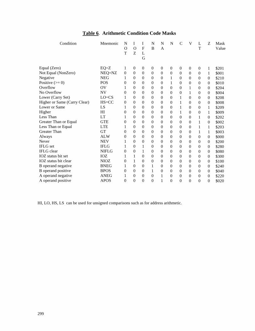
Table 6. Arithmetic Condition Code Masks
Condition
Mnemonic
N O T
I O Z
I F L G
N B
N A
N
C
V
L T
Z
Mask Value
Equal (Zero) Not Equal (NonZero) Negative Positive (>= 0) Overflow No Overflow Lower (Carry Set) Higher or Same (Carry Clear) Lower or Same Higher Less Than Greater Than or Equal Less Than or Equal Greater Than Always Never IFLG set IFLG clear IOZ status bit set IOZ status bit clear B operand negative B operand positive A operand negative A operand positive
EQ=Z NEQ=NZ NEG POS OV NV LO=CS HS=CC LS HI LT GTE LTE GT ALW NEV IFLG NIFLG IOZ NIOZ BNEG BPOS ANEG APOS
1 0 1 0 1 0 1 0 1 0 1 0 1 0 0 1 1 0 1 0 1 0 1 0
0 0 0 0 0 0 0 0 0 0 0 0 0 0 0 0 0 0 1 1 0 0 0 0
0 0 0 0 0 0 0 0 0 0 0 0 0 0 0 0 1 1 0 0 0 0 0 0
0 0 0 0 0 0 0 0 0 0 0 0 0 0 0 0 0 0 0 0 1 1 0 0
0 0 0 0 0 0 0 0 0 0 0 0 0 0 0 0 0 0 0 0 0 0 1 1
0 0 1 1 0 0 0 0 0 0 0 0 0 0 0 0 0 0 0 0 0 0 0 0
0 0 0 0 0 0 1 1 1 1 0 0 0 0 0 0 0 0 0 0 0 0 0 0
0 0 0 0 1 1 0 0 0 0 0 0 0 0 0 0 0 0 0 0 0 0 0 0
0 0 0 0 0 0 0 0 0 0 1 1 1 1 0 0 0 0 0 0 0 0 0 0
1 1 0 0 0 0 0 0 1 1 0 0 1 1 0 0 0 0 0 0 0 0 0 0
$201 $001 $210 $010 $204 $004 $208 $008 $209 $009 $202 $002 $203 $003 $000 $200 $280 $080 $300 $100 $240 $040 $220 $020
HI, LO, HS, LS can be used for unsigned comparisons such as for address arithmetic.
299
3.4. Instruction Cycle Execution Latency (Latent Instructions) This advanced topic may be skipped by the novice or the first-time reader.
This category of latency regards the latency of the instructions themselves. All the latent ESP2 instructions are from the ALU. No instruction has an execution latency which exceeds 1 instruction cycle. The latent instruction is one whose impact is not effective until the second queued program line following. The reason we study this topic is because we must be able to predict the effect of cascades of instructions, some of which may be latent. The latent instructions in the ESP2 are: Jcc, JScc, RScc, and BIOZ. The latent pseudo instructions are: BIOZNORFSH and HALT. The JMP class (Jcc, JScc, RScc) instructions always see the next queued instruction line execute prior to the actual branch; this is a prominent case. The HALT class (HALT, BIOZ, BIOZNORFSH) instructions see the next queued instruction line execute prior to freezing the PC; most all audio programs will employ the BIOZ instruction. In the following examples, the labels, identified by colons, each denote a PC value corresponding to a particular program line number. Many of the ancillary instructions are NOPs to make the examples simpler, but they generally represent any nonlatent instruction. CASE: JMP class An important instruction sequence involves the nonlatent low-overhead loop instruction, REPT, which is not from the JMP class. Specifically, we consider: CODE I1: NOP REPT label2, countm1 I2: NOP JMP label1 /* CMR unconditionally preloaded with ALW */ I3: NOP /* executed */ label1: NOP label2: NOP The outcome is that the REPT_ST SPR receives the value, I2, as expected. The loop spans the program lines I2 through label2. But now consider: CODE label1: NOP label2: NOP : : I1: NOP JMP label1 /* CMR unconditionally preloaded with ALW */ I2: NOP REPT label2, countm1 The outcome has changed such that the REPT_ST SPR receives the value, label1. This happens because when REPT is executed, the program line at label1 is queued next in line for execution; this is what is meant by the phrase, queued for execution. The loop now spans only label1 and label2. This feature permits the use of disjunct REPT blocks.
300

CASE: HALT class CODE I1: NOP HALT I2: NOP REPT label1, countm1_gpr > REPT_CNT label1: NOP /* loop */ This important exception is for one-line loops using the second form of the REPT instruction. The previous halt state disrupts the normal latency of the load to the REPT_CNT SPR. So our one-line loop rule for the second form of REPT reverts to the rule for the first form, and the concern about the address of countm1_gpr disappears. Since this is too difficult to remember, we recommend using only the first form of REPT for one-line loops (see REPT instruction description). ASSEMBLER NOTE: A warning should be issued under the circumstance that a HALT instruction precedes the second form of the REPT instruction used for a one-line loop. The warning states that countm1_gpr should not contain the number of repeats less one (i.e., not the number of loops desired less two); but rather, the number of repeats desired. If the instruction preceding REPT is BIOZ (or BIOZNORFSH) for this case, the outcome depends upon whether suspension actually occurs. Hence, this alternate warning should recommend not using the construct unless the programmer knows that suspension will always occur or always not occur. CASE: JMP class, JMP class Consider the example of two JMP class instructions, one after the other: CODE I1: NOP JMP label1 /* CMR unconditionally preloaded with ALW */ I2: NOP JMP label2 /* CMR unconditionally preloaded with ALW */ I3: NOP /* hurdle 1 */ label1: NOP I5: NOP /* hurdle 2 */ label2: NOP According to the prescribed latency of these instructions above, the sequence of executed program lines will be as follows: I1, I2, label1, label2. CODE I1: NOP JS label1 /* CMR unconditionally preloaded with ALW */ I2: NOP JMP label2 /* CMR unconditionally preloaded with ALW */ I3: NOP /* hurdle 1 */ : : label1: NOP I5: NOP /* hurdle 2 */ label2: NOP Here we find that the PC value I3 is pushed onto the hardware stack for the instruction sequence above; this is as expected.
301

CODE I1: NOP JMP label1 /* CMR unconditionally preloaded with ALW */ I2: NOP JS label2 /* CMR unconditionally preloaded with ALW */ I3: NOP /* hurdle 1 */ label1: NOP I5: NOP /* hurdle 2 */ : : label2: NOP But now we find that the instruction sequence above pushes I5 onto the stack. Again, this is because when JScc is executed, the instruction line at label1 is queued next in line. A number of academic examples can be constructed from a sequence of JScc/RScc instructions, but they are perhaps not very useful. The predominant feature of this particular sequence is the aerobatic trajectory of the PC. We give one such example: CODE NOP JS label /* CMR unconditionally preloaded with ALW */ NOP RS /* CMR unconditionally preloaded with ALW */ pcstack0: instruction0 /* hurdle */ label: instruction1 : In the example above, pcstack0 is pushed onto the hardware stack by JS. The program line holding RS is executed, then instruction1 is executed, and then instruction0 is executed. Then instruction1 is executed again before the program continues on. instruction1 is executed a total of two times, but instruction0 is executed only once. By inserting NOPs and/or moving the label around, many more such exercises can be generated. CASE: HALT class, HALT class Generally speaking, this type of instruction sequence is not useful and should not be programmed. For example, two HALT pseudo instructions cannot be queued because the impact of the second HALT will be lost upon restart by the system host. As a second example, consider a HALT/BIOZ sequence. The BIOZ instruction loses its execution latency as the chip becomes effectively 'suspended' indefinitely. When the ESP_HALT_EN bit is not set, the execution latency of BIOZ returns hence producing a different outcome. There is no useful purpose for this.
302
CASE: JMP class, HALT class The following instruction sequence is a useful programming paradigm (see the Applications section.): CODE top_of_program: NOP /* executes prior to suspension. */ I1: NOP /* PC frozen here. */ : : NOP JMP top_of_program /* CMR unconditionally preloaded with ALW */ NOP BIOZ I2: ... /* never executed */ Since both JMP and BIOZ are latent, the instruction line queued for execution following each is always executed before impact. The contiguous program line at I2 is never executed. The PC becomes frozen at the second queued instruction line following BIOZ if suspension occurs. When suspension terminates, execution will resume at instruction line I1. CASE: HALT class, JMP class This instruction sequence is automatically detected by the hardware as a special case. The HALT_JUMP monitor bit in the HOST_CNTL register goes high when the normal run-time latency of a JMP class instruction is being enforced following a HALT class instruction. The execution latency of a JMP might be absorbed by a preceding HALT class instruction were it not for this enforcement. So, from a programmer's point of view, a JMP class instruction has the same execution latency under all circumstances regardless of what instruction precedes it. We present this case here only in the interest of being complete. As an example: CODE NOP BIOZ I0: NOP JMP I2 /* HALT_JUMP bit stays high for this cycle. */ I1: NOP /* PC frozen here if it freezes. */ : /* hurdle */ : I2: ... Here the JMP instruction line at PC location I0 always executes prior to any amount of suspension time (including none) due to BIOZ. The instruction line at location I1 will execute following any suspension. But I1 always executes prior to the branch regardless of whether the state of suspension actually occurs; this is because of latency enforcement. After I1 executes, the PC will relocate to I2. Because a feature of the chip synchronization interface allows individual program loops to occasionally exceed the sample period, it is not desirable that the BIOZ instruction unequivocally cause suspension. It is for this reason that the enforcement is necessary.
303

4. Indirect Register Addressing A mechanism is provided for indirect addressing of internal register-type operands for the MAC unit (D, E, F), the ALU (A, B, C), and AGEN (G). Seven SPRs, corresponding to the six operands of the ALU and MAC unit and the one AOR operand of the AGEN (INDIRA, INDIRB, INDIRC, INDIRD, INDIRE, INDIRF, and INDIRG), act as pointer registers holding operand addresses. This mechanism indirectly accesses internal register data with normal latency once the pointer registers are loaded. To proceed with indirect register addressing, we must first load some internal register address into one (or more) of the pointer registers corresponding to the desired operand(s). To activate the indirection mechanism, an instruction is written substituting the INDIRECT SPR as the desired operand for which indirection should occur. This substitution can be for any (or all) of the seven instruction operands. The hardware will recognize this special INDIRECT SPR and substitute the contents of the corresponding pointer register (INDIRA,B,C,D,E,F,G) for the operand address. The INDIRECT SPR is not a physical register; it is a reserved address in the SPR space which is used by the programmer to activate indirection on a particular operand. Two more reserved addresses, INDIRINC and INDIRDEC, are provided which also accomplish indirection via the pointer registers. INDIRINC has the augmented functionality of post-incrementing the corresponding pointer register's contents. INDIRDEC post-decrements the corresponding pointer register's contents. (This can be very useful in looping on
internal array elements.) When automatically inc[dec]remented in that manner, the INDIRA, INDIRB, and INDIRC pointer SPRs each become an extra source and destination whose timing follows the ALU source and destination in the Instruction Cycle Timing diagram shown in Figure 2. Likewise, automatic inc[dec]rement of INDIRD, INDIRE, and INDIRF follow the MAC unit source and destination timing, while INDIRG inc[dec]rement follows AGEN source and UPDATE BASE timing. The inc[dec]remented pointer register contents will be available for the purpose of indirection in the next instruction cycle; i.e., these automatic inc[dec]rement operations are nonlatent, and normal inter-unit latencies apply. Miscellaneous If the function unit instruction whose indirection operand is specified as INDIRINC or INDIRDEC is actually skipped (as in conditional execution), then the automatic increment or decrement will not take place. We see in Figure 1 that the MAC unit's E operand has no access to AORs. Similarly, if INDIRE points to an AOR, the outcome is indeterminate. Indirection within the REPT instruction repeated block is not prohibited.
304

4.1. Exceptions to Indirection Since the ALU instructions, MOVcc, Jcc, JScc, RScc, and REPT, use the source operand fields of the instruction for storing Condition Mask and repeat count values, the indirection mechanism is disabled in the hardware for those particular source types to avoid unexpected results. This could hypothetically occur if one of the afflicted source operand fields were to contain a value which matched the INDIRECT, INDIRINC, INDIRDEC, or REF reserved addresses. Table 7 lists the afflicted instructions showing the operands for which indirection is available * :
Table 7. Indirection Operand Availability
Instruction Operand A Operand B Operand C MOVcc * * Jcc * n/a JScc * n/a RScc * * REPT * n/a ASSEMBLER NOTE: The assembler should detect the use of the REF, INDIRECT, INDIRINC, and INDIRDEC keywords as the B operand of REPT, or the A operand of MOVcc, Jcc, JScc, and RScc and then warn the programmer that indirection is disabled for those operands. ASSEMBLER NOTE: In the * cases of Jcc, JScc, and REPT, there are four high instruction addresses which cannot be directly referenced as PC values. These illegal instruction addresses correspond to the register addresses of INDIRECT, INDIRINC, INDIRDEC, and REF. In these cases it is the PC value that is detected as an error, while the use of the four keywords is legal; the REF keyword draws an 'outcome indeterminate' warning, however. ASSEMBLER NOTE: The values for the INDIRECT, INDIRINC, and INDIRDEC reserved addresses are all 10-bit values having 1 in the MSB. The G operand field of the instruction is only 9-bits wide. But, since the G operand field always refers to AORs, the 10th bit of this field is implicitly a 1. PROGRAMMER NOTE: In order to use indirection effectively, always use the verbose form of the instructions using no implicit destinations. ASDH, ASDL, LSDH, and LSDL require special consideration regarding indirection. See those instructions for information. Admittedly our method of indirection is contrived. The motivation was the primary design objective that makes all instructions execute in one cycle.
305
4.2. Pointer Register Latencies Since the contents of the INDIRA,B,C,D,E,F,G pointer SPRs are used as operand addresses rather than as operands, the latencies encountered when these registers are modified as normal destinations differ from the inter-unit latencies described elsewhere. These latency rules are as follows: Nonlatent 1. The result of a MAC unit write to INDIRA,B,C is available for use as an indirect address no sooner
than 1 instruction cycle (1 queued program line) later. Latent 2. The result of a MAC unit write to INDIRD,E,F,G is available for use as an indirect address no sooner
than 2 instruction cycles later. 3. The result of an ALU unit write to INDIRA,B,C,D,E,F,G is available for use as an indirect address no
sooner than 2 instruction cycles later. __________________ A programmer's chart can be found in the ESP2 Language and Software Specification.
306

5. Internal Memory Refresh The majority of internal memory is implemented in Dynamic RAM (DRAM) and, therefore, requires a periodic refresh of its contents. This consideration applies to the instruction memory, the GPRs, and the AORs. Memory refresh might interfere with write access from the host interface or with memory writes made in the course of executing some typical ESP2 program were it not for dedicated hardware that transparently detects and prevents such collisions. The decision to use DRAM for selected memory functions greatly increased the amount of internal memory. The SPRs (Special Purpose Registers) are implemented as Static RAM (SRAM), so they do not require refresh.
5.1. Instruction Refresh Collision free instruction refresh is transparent to the programmer insofar as it happens nearly all the time; including suspension and halt. There are 4 memory accesses available in the instruction array per instruction cycle; these consist of two reads and two writes. Only 1 read is required for instruction fetching based on the PC, leaving three accesses available. 1 read and 1 write are used to allow host access to instructions when a host access is pending, or to perform refresh when no host access is pending. The remaining write access is unused. Refresh is performed based on the REFINST SPR which is a 10-bit counter. Although the current implementation of the chip has 300 instructions, the counter is allowed to count from 0 to 1023 for future expandability of the instruction array. Since each instruction is refreshed once every 1024 instruction cycles, the refresh period at 100nS/instruction is 102.4 uS. A bit in the HARD_CONF SPR can be used to enable or disable instruction refresh; the INST_REF_DIS bit disables instruction refresh when set (this is not desirable).
5.2. GPR and AOR Refresh The GPR array allows 6 accesses per instruction cycle: 4 for reading source operands to the ALU and MAC unit, and 2 for writing results of ALU and MAC unit operations. The AOR array allows 6 accesses per instruction cycle: 1 for reading a source operand to the AGEN, 3 for reading source operands to the ALU and MAC unit, and 2 writes of ALU and MAC unit results. In both the GPR and AOR array there are no available accesses for refreshing these internal registers. Host access is governed by the ALU timing. Refresh of internal registers at run-time is accomplished via common instructions invoking SPRs tied to hardware support of the refresh operation. (Recall that SPRs are static.) Those instructions provide refresh as an ALU function, NOP, BIOZ, HOST, and as a MAC unit function, RFSH, which each employ the indirect addressing hardware support provided by the REF and REFPT SPRs. We conservatively and empirically estimate a refresh rate of 5 kHz to be sufficient. The refresh mechanism should be transparent to the programmer because it is built in to the most commonly used instructions, but some unusual user programs may warrant its consideration. In normal audio signal processing applications, use of the BIOZ instruction for sample rate synchronization, and available ALU NOP pseudo instructions should provide sufficient refresh. Additional refresh can be provided through use of the HOST instruction or by using the MAC unit RFSH pseudo instruction instead of NOP in places where preservation of MACRL is unnecessary. The SPRs, REF and REFPT, control the refresh mechanism as follows: The reserved SPR address called REF provides an indirect addressing mechanism. By addressing REF in the operand field of an instruction, the content of REFPT is substituted as the operand address. REFPT is a 10-bit counter which post-increments whenever the REF reserved address is used as an ALU or MAC unit source operand address in an instruction, regardless of whether that instruction is actually skipped. Any successful (not
307

skipped) move of REF to REF via either the ALU or MAC unit accomplishes one refresh that cannot be inhibited. The newly incremented REFPT value is not available as the destination address until the time at which the current destination address is decoded for the function unit that caused the increment. The assertion of HALT_REF_DIS in the HARD_CONF SPR can never override the use of the REF SPR, used as source and destination, as a means to effect internal register refresh. Two moves of REF to REF on the same instruction line using both the ALU and MAC unit doubles the refresh rate. Because of the address mapping of GPRs from 0 to 455, and AORs from 512 to 963, the LSB of the REFPT counter serves as the MSB of the address so that refreshes alternate between GPR and AOR. Although REFPT is a 10-bit counter, the count is limited to the number of GPRs and AORs physically residing on the chip in the current version.
5.2.1. Internal Register Refresh during Suspension/Halt
The MAC unit and the ALU can both be used to perform internal register refresh operations simultaneously which doubles the refresh rate. When the chip is in the state of suspension (BIOZ bit of the HOST_CNTL register is set) or in the halt state (because of a high halt bit in the HOST_CNTL register), the MAC unit executes NOPs by default (designed to preserve MACRL) while the ALU executes the HOST instruction which allows host access or refresh when no access is pending. In these two states, the MAC unit can be forced to do refresh automatically by setting the HALT_MAC_REF bit in the HARD_CONF SPR. This has the effect of doubling the refresh rate, but the contents of the MACRL SPR will not be preserved. When the ESP2 program resumes (i.e., comes out of halt or suspension) the MACRL will subsequently be preserved, assuming no RFSH instructions in the MAC unit code. The HALT_REF_DIS bit in the HARD_CONF SPR can be set to disable internal register refresh by both the MAC unit and ALU during halt or suspension (this is not desirable). The assertion of HALT_REF_DIS always overrides the HALT_MAC_REF bit.
5.2.2. Internal Register Refresh Collision Due to the interleaved nature of the MAC unit and ALU operand fetching, one of these function units can be writing a new result to some internal register at the same time that the other unit is being used to refresh it. This consideration is also applicable to the case of host access, whose buss timing is governed by the ALU, either through the HOST instruction or during the suspension or halt states. The chip contains logic to prevent a refresh operation from writing old data over newly created register contents. Whenever REF is used as the destination in the MAC unit, the chip compares the contents of REFPT to the destination address of the ALU from the preceding instruction cycle. If the values are equal and the ALU instruction is not actually skipped (as in a conditionally executed instruction), a NOP is performed by the MAC unit instead of RFSH. Likewise, when REF is used as the destination in the ALU, the chip compares the contents of REFPT to the destination address of the MAC unit from the same instruction cycle. If the values are equal and the MAC unit instruction is not actually skipped, a NORFSH pseudo is substituted in place of NOP in the ALU.
308

6. SPR Hazards Many of the SPRs in the chip provide special dedicated services which require modification of the SPR contents as a result of ALU or AGEN operations. In those cases these registers are being modified by means other than their usage as the destination operand of some instruction. All SPRs can be read and written by the MAC unit and the ALU (with the exception of a handful of registers which are read-only or write-only). A conflict (a hazard) can occur at instances in which a particular SPR is modified in association with its special service at the same time that it is written as the destination of some MAC unit or ALU operation. The cases are all listed below: ASSEMBLER NOTE: The assembler should detect these hazards and issue errors (or warnings) because the outcome of these cases is indeterminate. 1. Specifying the CMR as the MAC unit destination on the same instruction line as an ALU Jcc, JScc,
RScc, or MOVcc. 2. Specifying the PC as the MAC unit destination at any time. 3. Specifying REPT_ST, REPT_END, or REPT_CNT as the MAC unit destination on the same
instruction line as an ALU REPT (or EXIT pseudo) instruction, or on the last line of a REPT block. 4. Specifying the PCSTACK0,1,2,3 SPRs as the MAC unit destination on the same instruction line as a
JScc or RScc. 5. Specifying a JScc, RScc, or Jcc on the penultimate queued instruction line of a REPT block. 6. Specifying a region BASE SPR as a MAC unit destination on the same instruction line as the AGEN
performing an UPDATE BASE operation on the same register. 7. Specifying either SPR, HOST_GPR_DATA or HOST_ESP_FACE, as a MAC unit destination at any
time should be cited because it could cause conflict with a host write to that register as a host interface register. (warning)
There is a conflict specifying HOST_CNTL_SPR as a MAC unit source at any time because the host may be writing to it as an interface register at the same time that the MAC unit is reading from it. (warning)
8. Specifying CCR as the MAC unit destination when the ALU operation on the same instruction line is
not MOV (or NOP), MOVcc, Jcc, JScc, RScc, HOST (HOSTNORFSH), BIOZ (BIOZNORFSH), or REPT. (warning)
Specifying CCR as the ALU destination of an instruction which is not MOV, MOVcc, RScc, HOSTNORFSH, or BIOZNORFSH. (warning)
9. The indirection mechanism provides an automatic increment or decrement of the pointer SPRs via the
INDIRINC and INDIRDEC SPRs. Consequently, the following indirection hazards can occur: 1) MAC unit write to INDIRG on the same program line as an AGEN reference to INDIRINC or
INDIRDEC. 2) MAC unit write to INDIRD when the D operand is INDIRINC or INDIRDEC, or to INDIRE when
the E operand is INDIRINC or INDIRDEC. ALU write to INDIRA when the A operand is INDIRINC or INDIRDEC, or to INDIRB when the B operand is INDIRINC or INDIRDEC.
3) MAC unit write to INDIRINC or INDIRDEC when INDIRF points to itself. ALU write to INDIRINC or INDIRDEC when INDIRC points to itself. (This last MAC and ALU hazard is not detectable by the assembler, in general.)
309
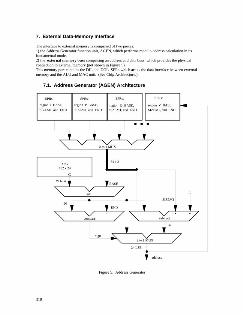
7. External Data-Memory Interface The interface to external memory is comprised of two pieces: 1) the Address Generator function unit, AGEN, which performs modulo address calculation in its fundamental mode, 2) the external memory buss comprising an address and data buss, which provides the physical connection to external memory (not shown in Figure 5). This memory port contains the DIL and DOL SPRs which act as the data interface between external memory and the ALU and MAC unit. (See Chip Architecture.)
7.1. Address Generator (AGEN) Architecture
add
AOR 452 x 24
G
8 to 1 MUX
compare subtract
BASE
END
SIZEM1
2 to 1 MUXsign
address
SIZEM1, and END SIZEM1, and END SIZEM1, and END
SPRs:
region V BASE,SIZEM1, and END
24 x 3
W buss
1
24 LSB
26
26
SPRs:SPRs:SPRs:
region Q BASE,region P BASE,region I BASE,
- - -
Figure 5. Address Generator
310

A partial diagram of the Address Generator unit is shown in Figure 5. The Address Generator calculates absolute addresses for the external memory interface once every instruction cycle (100nS). It consists of three 26-bit adders, eight BASE SPRs, eight END SPRs, and eight SIZEM1 SPRs, the 24-bit unsigned SPRs serving to partition eight addressing regions. Relative address offsets held in 24-bit unsigned AORs are selected by the G operand field of the instruction. The programmer dereferences an AOR to make an indirect access of external memory. AGEN code can be automatically generated for the programmer by the assembler. Three bits in the external-memory control-field of the micro-instruction determine which of the eight regions is accessed. The programmer's code either states the desired region, or it is implicit from the declaration of the AOR. The memory location and purpose of the eight regions are each determined by the contents of the corresponding region control registers (BASE, SIZEM1, and END). The region control registers can be automatically initialized by the assembler from values implicit in the programmer's region declarations. These regions can each be configured as delaylines, tables, or I/O space through the appropriate setting of the region control registers. This becomes apparent by examining the nature of the calculations automatically performed in the AGEN:
7.1.1. AGEN Address Calculation At every instruction cycle the following external memory address calculations are performed using the specified address offset register and the region control registers from the region specified in the micro-instruction. address = AOR + BASE if address > END
address = address - (SIZEM1 + 1) 'address' is an absolute external memory address. AOR denotes one of the Address Offset Registers. The SIZEM1 SPR contains the size of the region - 1; this deficit is necessary in order to represent a table which is the full size of physical memory, and accounts for the correction factor '1' appearing in Figure 5. Although the BASE, SIZEM1, END, and AOR are 24-bit unsigned, the calculations are carried out at 26-bit two's complement to prevent the first equation from overflowing and to guarantee the correct sign in the result of the comparison.
7.1.2. Plus-One Addressing Mode The first calculation can also be executed as address = AOR + BASE + 1 under instruction control. This addressing mode (not shown in Figure 5) is useful in acquiring neighboring addresses as for interpolation operations. No register is permanently modified as a result of this calculation which occurs prior to external memory access.
311

7.1.3. Extent of the Modulo These equations allow circular addressing within a predefined region because of the region END detection and modulo addressing. This modulo scheme of addressing restricts the AOR offset range to 0 through SIZEM1 + 1, for any value of BASE within the modulus. Since the modulo does not go to infinity, it is easy for computed AOR offsets to land outside of the modulus, so programmers should beware. Regions can reside anywhere in physical memory based on the contents of the region control SPRs. Regions cannot span absolute address zero. Multiple delaylines coexist in the same region by stringing them end to end and addressing them using different offsets within the modulus. Delaylines will move only within the extent of the defined region by decrementing the region BASE in a modulo fashion described in the section UPDATE region BASE. Therefore, the operation of delaylines will not impact data in other regions of memory. Modulo addressing is always with respect to the region, not to the individual delayline.
7.1.4. Other External Memory Configurations
By setting the END SPR to the value of the maximum physical memory location, the region simplifies to a table not having modulo addressing. Tables are distinguished from delaylines by fixing the BASE SPR. In this case the BASE always points to the first location of the table. Tables can certainly be implemented, however, without defeating the modulo addressing hardware scheme. Setting BASE to zero and END to the value of the maximum physical location defeats modulo addressing while admitting absolute addressing, in the AORs, suitable for peripheral I/O devices. The recommended use of AORs is to hold relative address offsets with respect to the associated region. I/O addressing can certainly be implemented in a relative fashion without the need to defeat the modulo addressing hardware. In any case, for absolute addressing the MUX_ADDR bit in the HARD_CONF SPR must be low (linear addressing). All these configurations can be determined by the programmer in the declarations. (See the Software Spec. for more.)
7.1.5. UPDATE region BASE A built-in method for updating the region BASE SPR under program control is also provided via the AGEN. This mechanism is especially useful for decrementing the BASE register every sample period in a modulo fashion. This is desirable when programming delaylines. As before, the AGEN calculates a new address using the contents of the AOR (pointed to by the G operand field) as the offset amount. The only change is that the AGEN opcode field of the instruction demands that the address be written to the external address buss as well as back into the BASE SPR. The AOR, in this addressing mode, becomes a post-increment to the region BASE SPR. This explains the feedback path in Figure 5. address = AOR + BASE if address > END
address = address - (SIZEM1 + 1) BASE = address The new BASE value is available to the MAC unit, ALU, and AGEN on the next instruction cycle for use both in AGEN addressing and as a source SPR. To modulo decrement the BASE by 1, set AOR equal to contents of SIZEM1. To decrement the BASE by 2, set AOR equal to SIZEM1 - 1, and so on. Decrementing can be performed indefinitely, the BASE remaining within the modulus. ASSEMBLER NOTE: If BASE updating is specified in a given instruction, a collision could occur between the AGEN and the MAC unit trying to write to the same region BASE SPR because the two units are operating with the same timing. This hazard should be recognized and flagged as an error by the assembler; chip operation is unpredictable.
312

7.2. AGEN Instructions The AGEN opcode field consists of six instruction bits. Three of the bits are used for selecting one of eight regions. The remaining three bits are used to select from the following operations: NOP cycle on the external memory buss. External memory RD. External memory RD, then UPDATE BASE. Plus-One addressing, external memory RD. External memory WR. External memory WR, then UPDATE BASE. Plus-One addressing, external memory WR. UPDATE BASE. During an AGEN NOP, the external memory buss is tristated. The last operation (UPDATE BASE) allows UPDATE of the region BASE SPR while tristating the external memory buss. See the ESP2 Language and Software Specification for the proper syntax of AGEN instructions.
7.3. Accessing the Region Control Registers and AORs The region control registers (BASE, SIZEM1, and END) are mapped as SPRs for use as source/destination operands by the ALU and MAC unit. This can be useful for having more than eight physical regions of external memory active at a time, since the contents of these registers can be modified under program control. In the assembler, the regions are called I,P,Q,R,S,T,U,V. These are respectively assigned in microcode to: 0,1,2,3,4,5,6,7. So references to BASEP, SIZEM1U, or ENDT, for example, denote a region control SPR in a particular region. The AORs can also be accessed by the ALU and MAC unit for computing address offsets in the running program. The ALU provides the ADDV and SUBV instructions for unsigned arithmetic operations. Because of bandwidth limitation on the AOR memory, AORs cannot be used as the E operand of the MAC unit. (Refer to the section on Register Usage.) When AORs are not being used to hold address offsets, they can be used for any general purpose. See the Pipeline section in the Software Spec. for a simple chart of latencies in the access of the registers discussed above.
7.4. External Memory Access
The external memory interface port consists of a 24-bit address buss, a 24-bit data buss, the pin signals Row Address Strobe (RAS\), Column Address Strobe (CAS\), Memory Read/Write (MR/W\), and Memory Request (MEM_REQ\). The MEM_REQ\ pin is asserted by the ESP2 to signal an upcoming external memory cycle. When the MEM_REQ\ signal is asserted, the CAS\ and RAS\ signals of the ESP2 will assert during the next memory cycle. The MEM_REQ\ and MR/W\ pins each require a pull-up resistor.
313

CLK
RAS\
CAS\
MADDR
MR/W\
MDATA
EM_REQ\
1 2 3 4 1 2 3 4 1 2 3 4 1 2 3 4 1 2 3 4
NOP RD NOP WR NOP/exo.
address
ESP2 External Memory Access Timing
row column
(muxed) (static)
LOW
hiZ
HIGH
valid
ESP2 RD ESP2 WR exogenous
Tstate
memorycycle
datadata
LOW
hiZ
HIGH
Figure 6. Timing with refresh disabled. The MUX_ADDR bit selects the multiplexed or static addressing modes on-the-fly. The timing diagram in Figure 6 illustrates activity on the memory buss over five instruction cycles for several operations. One instruction cycle corresponds to four Tstates which corresponds to one memory cycle. Since addressing can be either multiplexed (DRAM) or linear (SRAM), the diagram shows both forms. The signals RAS\ and CAS\ are asserted regardless of whether multiplexed or linear addressing is performed. This is because the RAS\ signal is sometimes used for chip-enable while CAS\ is sometimes used for output-enable of static RAM chips. In the event that the RAS low time provides insufficient access time for SRAMS, an upper address line with a resistor pullup can serve as a chip select providing a 3.5 clock cycles worth of access time. Notice how the MR/W\ and MEM_REQ\ signals are driven high by ESP2 before and after there assertion by the ESP2. Driving high at the end of the cycle ensures good rise time characteristics as opposed to a resistor pullup. These signals should have resistor pullups to hold them high while they are tristate by the ESP2 The ESP2 will tristate (release) the pin signal MR/W\ and the external memory buss (address and data) during AGEN NOP or UPDATE BASE (no access) instruction cycles, and also during halt state and BIOZ suspension where the AGEN is designed to execute NOPs. This feature can be used to allow exogenous hardware or other running ESP2 chips access to the same external memory. Since the MEM_REQ\ pin tristates during unused cycles, it can be driven by exogenous hardware to force the ESP2 to generate a RAS\/CAS\ sequence on the very next memory cycle. The assertion of MEM_REQ\ by an exogenous source does not force the ESP2 to release the external memory buss, so buss contention is possible. For this reason it is recommended to allow access by an exogenous source only during the halt and indefinite suspension states. When multiple ESP2s are set up to share the same external memory, however, one of the chips can automatically drive the RAS\ and CAS\ pins by watching its MEM_REQ\ input pin which is wire-ORed
314

between all the running ESP2s. The memory accesses must be scheduled in the AGEN code of each chip so as to avoid buss contention. This presumes that the chips are running in synchronization with one another which can be accomplished by a system reset.
7.4.1. External Address Buss The external memory address buss is controlled by the ESP2 for the purpose of supplying a 24-bit address to external memory and peripheral I/O devices. A bit-selectable mode is available on-the-fly which provides multiplexed addressing (RAS\/CAS\) for accessing dynamic RAM (DRAM), in sizes from 64K to 16M, when the MUX_ADDR bit in the HARD_CONF SPR is high (set). Otherwise (reset), linear addressing for static RAM (SRAM) or peripheral I/O is selected. When the MUX_ADDR bit is asserted from the MAC unit, the new AGEN addressing mode is activated immediately (i.e., in the same instruction cycle). If asserted from the ALU, the new addressing mode is activated on the next instruction cycle. Multiplexing is illustrated in Table 8 for DRAMs of various sizes. The Table shows what actually appears at the address pins when either mode is selected. For example; when a 256K by n-bit DRAM is connected, what actually appears at the ESP2 address pin called A8 is the address bit A0 when RAS\ (Row Address Strobe\) is asserted, and address bit A16 when CAS\ (Column Address Strobe\) is asserted. The wordlength, n, of the physical DRAM does not impact the address pin connections. Further, DRAMs of various size may coexist in a system. The address pin names, MADDR[23:0], have been shortened in the Table.
Table 8. External Address Pin Connection
PIN NAME
A23 A22 A21 A20 A19 A18 A17 A16
A15 A14 A13 A12 A11 A10 A9 A8
A7 A6 A5 A4 A3 A2 A1 A0
SRAM mode: linear
A23 A22 A21 A20 A19 A18 A17 A16
RAS\/CAS\ size: any
A15 A14 A13 A12 A11 A10 A9 A8
A7 A6 A5 A4 A3 A2 A1 A0
DRAM multiplexed
A23 A22 A21 A20 A19 A18 A17 A16
RAS\/CAS\
any
A11/A23 A3/A22
A10/A21 A2/A20 A9/A19 A1/A18 A8/A17 A0/A16
A7/A15 A6/A14 A5/A13 A4/A12 A3/A11 A2/A10 A1/A9 A0/A8
DRAM multiplexed
A23 A22 A21 A20 A19 A18 A17 A16
RAS\/CAS\
64K
A7/A15 A6/A14 A5/A13 A4/A12 A3/A11 A2/A10 A1/A9 A0/A8
DRAM multiplexed
A23 A22 A21 A20 A19 A18 A17 A16
RAS\/CAS\
256K
A8/A17 A0/A16
A7/A15 A6/A14 A5/A13 A4/A12 A3/A11 A2/A10 A1/A9
DRAM multiplexed
A23 A22 A21 A20 A19 A18 A17 A16
RAS\/CAS\
1M
A9/A19 A1/A18 A8/A17 A0/A16
A7/A15 A6/A14 A5/A13 A4/A12 A3/A11 A2/A10
DRAM multiplexed
A23 A22 A21 A20 A19 A18 A17 A16
RAS\/CAS\
4M
A10/A21 A2/A20 A9/A19 A1/A18 A8/A17 A0/A16
A7/A15 A6/A14 A5/A13 A4/A12 A3/A11
DRAM multiplexed
A23 A22 A21 A20 A19 A18 A17 A16
RAS\/CAS\
16M
A11/A23 A3/A22
A10/A21 A2/A20 A9/A19 A1/A18 A8/A17 A0/A16
A7/A15 A6/A14 A5/A13 A4/A12
The DRAM sizes shown in Table 8 are typical of the industry standards. Since DRAM address pins are multiplexed, every pin added increases memory size by a factor of 4. Typical DRAM chips may not be fast enough to interface to the ESP2 running at full speed. The DRAM access time must be at most 50 nS when running the ESP2 at the system clock rate of 40 MHz (10 MHz instruction rate). Slower DRAM demands a slower clock rate. Very high speed SRAM is commonly available, hence the two address buss modes.
315

The external memory buss is asserted for every AGEN instruction type excepting a NOP and an UPDATE BASE (no access) instruction. Since those two operations do not access external memory, the address and data buss are tristated. The external memory buss is also tristated during halt or when the chip is in suspension due to the BIOZ instruction, for then the AGEN is performing NOPs.
7.4.2. External Memory Data-Interface
The interface from the chip's internal computation units (MAC and ALU) to external memory is supplied through the AGEN's Data Input Latches (DILs) and Data Output Latches (DOLs). A 4-bit field in the micro-instruction along with a read/write bit identifies one of these registers to AGEN. The assembler can organize the use of these registers into FIFO and cache structures. There are 16 DILs and 16 DOLs, all 24 bits wide and mapped as SPRs. These registers are accessed by the computation units as sources and destinations like any other SPR. The AGEN provides a feature called magnitude truncation (to 16 or 24 bits) of DOL out to external memory. The 24-bit DOL is assumed to hold the MSBs of a larger word in two's complement. Magnitude truncation to 24 bits or less is desired. This feature is controlled by two bits in the HARD_CONF SPR: The MAG_TRUNC bit enables magnitude truncation when it is high. When set from the MAC unit, magnitude truncation becomes active on the same program line. When set from the ALU, magnitude truncation is activated on the next queued program line. The TRUNC_WIDTH bit sets the truncation width to 24-bits when it is high, or 16-bits when it is low. In the case of 24-bit truncation width, the magnitude truncation algorithm is as follows:
if (DOL < 0) external memory = DOL + $1 else external memory = DOL
In the case of 16-bit truncation width, the algorithm is: if (DOL < 0) external memory = (DOL + $100) & $FFFF00 else external memory = DOL & $FFFF00 For 16-bit truncation width, the 8 LSBs of the 24-bit result are set to $00 which allow development of algorithms for 16-bit target systems within development systems having 24-bit external memory. The selected algorithm is performed in the AGEN as DOL is sent out to external memory; the DOL is not permanently modified. For magnitude truncation somewhere in between 16 and 24-bits, one can employ the various shifting mechanisms in the computation units prior to magnitude truncation.
316

7.5. External DRAM Refresh
1 2 3 4 1 2 3 4 1 2 3 4 1 2 3 4 1 2 3 4
disabled CAS\ before RAS\ ESP2 acc. NOP/exo. RAS\-only
ESP2 External Memory Refresh Timing
LOW
hiZ
HIGH
ESP2 access exogenous
CLK
RAS\
CAS\
MADDR
MR/W\
MDATA
MEM_REQ\
R/W\
memorycycle
Tstate
data
row column
(muxed)
LOW
hiZ
HIGH
refresh NOP/ NOP/NOP/
Figure 7. Refresh enabled after first cycle. Refresh is associated with AGEN NOP when there is no MEM_REQ\ on the previous cycle. The ESP2 supports both DRAM and SRAM as external memory, and both memory types may be coexistent in a system design. There exists an automatic external DRAM refresh mechanism built into the ESP2. This mechanism acts in conjunction with the address counters built into most all commercial DRAM chips. The DRAM's address counter controls a refresher, also inside the DRAM chip, which becomes activated by the appearance of the pin signal CAS\ before the pin signal RAS\. ESP2 supports the CAS\ before RAS\ refresh mode for total refresh. Notice in Figure 7 how the MR/W\ signal is driven high by ESP2 during a refresh cycle. Depending upon the system design when SRAM is present, be aware that the refresh mechanism may cause a read of SRAM, putting data on the external memory buss. A second mode of refresh, RAS\-only refresh, is not fully supported by ESP2 because it requires a refresh address to appear on the external memory buss. The RAS\-only refresh signal can be made to emanate from the ESP2 RAS\ pin, however. Do not allow the address buss to become undefined during a RAS\-only refresh as this can corrupt DRAM regardless of the state of the MR/W\ or CAS\ lines. These two modes of refresh are determined by the settings of two bits in the HARD_CONF SPR. The XMREF_CASDIS bit, when set, yields RAS\-only refresh. When the XMREF_DIS bit is set, both modes of refresh are disabled. (XMREF_DIS overrides XMREF_CASDIS.) Both bits low yield the default mode, CAS\ before RAS\ refresh. All settings are independent of the MUX_ADDR bit. When activated, the ESP2 external DRAM refresh mechanism operates transparently at run-time, halt, or during BIOZ suspension. At run-time the refresh mechanism engages only when the AGEN unit is executing NOP or UPDATE BASE (no access) instructions and the MEM_REQ\ pin signal was not asserted by any source (exogenous or ESP2 itself) on the previous memory cycle. During halt or suspension, recall that the AGEN executes NOPs, so refresh will automatically occur on every memory cycle as long as the MEM_REQ\ signal was not asserted on the previous cycle. Recall that the act of reading or writing external memory at N sequential locations over a specified time period also accomplishes total refresh, where N is the square root of the external DRAM size.
317

Note that if an exogenous device takes over the external memory buss and exercises MEM_REQ\, it will prevent ESP2 from refreshing DRAM. If the external memory buss is usurped for extended periods, the exogenous device must be responsible for refreshing DRAM.
7.6. Initializing or Accessing External Memory from the System Host
The ESP2 does not provide internal hardware for direct access of external memory by the system host through the ESP2. The ESP2 tristates its external memory buss during the states of halt and BIOZ suspension, and during NOP or UPDATE BASE (no access) instruction execution in the AGEN. It is at these times that exogenous hardware (e.g., the host itself) can be given direct access to external memory over that same buss. If we allow the host to take-over the ESP2 external memory buss, then when external DRAM is used and there is no MEM_REQ\ pin signal assertion from either the ESP2 or the host, the DRAM will always be automatically refreshed by ESP2 on the next memory cycle if the CAS\ before RAS\ refresh mode is activated in the HARD_CONF SPR. To avoid buss contention with a running ESP2 program making random access, it may be preferred to transfer external memory data to/from the host (or some DMA
mechanism) during halt or indefinite suspension. But if the transfer needs to occur at run-time, various methods may be employed which require a very simple ESP2 program to supervise indirect transfer through the ESP2: One such procedure might incorporate the ALU BIOZ instruction. This instruction indirectly monitors the IOZ input pin from the synchronization interface. The IOZ pin will typically be hardwired to the sample rate clock (LRCLK). The implication here is that were the IOZ pin involved in the transfer of audio data to/from external memory, then the transfer could occur no faster than the system sample rate. Under these assumptions, the standard host/ESP2-register interface would most likely be used. In that case, some GPR would be designated to hold the transferred data while some AOR would be designated to hold the external memory address offset. Of course some protocol would need to be established between the host and the ESP2 program, but this protocol is malleable. A second procedure might incorporate the IFLAG and OFLAG pins from the synchronization interface. There is no dedicated ALU instruction to monitor that input pin, but an image of the IFLAG pin appears in the CCR. There it is called IFLG and is updated on a per instruction basis. Therefore the IFLAG pin can be easily monitored by the ESP2 program based on the IFLG and NIFLG Conditions. Using this scheme, data would be transferred to/from the 8-bit HOST_ESP_FACE_B2,1,0 host interface registers. The ESP2 would transfer data directly into or out of the concatenated 24-bit SPR image (HOST_ESP_FACE) of these registers, bypassing the standard host/ESP2-register interface. The ESP2 could then signal back to the host via the OFLAG pin. Of course, some software protocol between the host and the ESP2 program would need to be established. This second procedure has the advantage that data transfer occurs at the instruction rate. It may be likely that these two procedures would find use while the chip is executing some application program. So, some scheme must be invented to vector the running ESP2 program to this external memory host-access routine after it has been overlaid. Vectoring by host load of the PC at run-time, using the standard host/ESP2-register interface, is not recommended because of indeterminate results. An alternative vectoring procedure is given in the Applications section.
318
8. Serial Interface The asynchronous serial interface consists of 16 24-bit serial data SPRs (called SER0L, SER0R, SER1L, SER1R, ..., SER7R), each L/R pair of which can be used for input or output to A/Ds, D/As, other DSP chips, etc. These SPRs are grouped into eight stereo pairs, each pair multiplexed on its own serial data pin (SER[0:7]). The SER data SPRs are double buffered so that both left then right channel data coming into the chip in one sample period are accessible to the ESP2 at the start of the next sample period. Likewise, data written to the left and right SER data SPRs by ESP2 during one sample period will be sent out in the next sample period, left channel followed by right. That is to say, there exists a latency equal to one sample period for serial data input or output. This design allows ESP2 access to SER data SPRs at any time throughout the sample period with no hazards. Each of the individual serial data pins (SER[0:7]) can be programmed as input or output, and each can be assigned to either of two sets of asynchronous serial clocks (LRCLK, WCLK, and BCLK) via the SER_CONF SPR. This accommodation for simultaneous communication between devices having different serial timing requirements opens the door to applications such as sample rate conversion.
8.1. Serial Interface Control Registers Because of the great diversity of definitions for serial clock timings amoung the commercially available D/As and A/Ds, the best approach is to make the serial interface fully programmable. The serial interface can be made to conform with I2S justification or the popular 'right justified' format. Format programmability can be achieved using a BCLK counter and the following serial interface control registers:
Table 9. Serial Interface Control Registers
WCLKL_ST WCLKL_END LRCLK_END WCLKR_ST WCLKR_END LRCLK_MOD
Defines the start of WCLK and left serial data. Defines the end of WCLK and left serial data. Defines the end of LRCLK. Defines the start of WCLK and right serial data. Defines the end of WCLK and right serial data. Defines the count modulus less 1 of the BCLK counter.
See the example for settings rules. By duplicating the BCLK counter and serial interface control registers, two independent timing sets are created with each serial data line assigned to either timing set. These 8-bit serial interface control registers are concatenated into SPRs called SCLK0_REG0 and SCLK0_REG1 both defining timing set 0, and SCLK1_REG0 and SCLK1_REG1 defining timing set 1; see those SPRs for the exact format. Observing the layout of the HARD_CONF SPR (see the section on Special Purpose Registers), any of the BCLK[0:1], and/or WCLK[0:1], and/or LRCLK[0:1] serial clock signals may be selectively enabled to drive the associated pins. When any of those signals are not enabled, the associated pin becomes a high impedance input. Any subset of the ESP2 serial clock pin signals may be selected as inputs independent of all the other clock pins.
319
8.2. LRCLK The LRCLK (left right clock) signal determines the channel, left or right. If the ESP2 is driving the LRCLK pin, it will assert (rise) after the BCLK counter reaches the value in LRCLK_MOD (see the example). Due to that assertion the BCLK counter resets and begins the count again, counting the number of bit clocks since the beginning of the sample period marked by the rising edge of LRCLK. The falling edge of LRCLK is defined by LRCLK_END. The BCLK counter will reset whenever the LRCLK signal transits high no matter who is driving the associated LRCLK pin. The SER data SPRs are latched as well on the positive transition of LRCLK. The system sample rate can be defined by LRCLK as generated by ESP2. If this is desired, then the exact rate can be expressed in terms of: 1)the system clock (CLK), 2)the BCLK modulus (LRCLK_MOD+1), and 3)the BCLK divide rate set in the HARD_CONF SPR. See Figure 8. When some other device is driving the LRCLK pin, it is not a requirement to load the LRCLK_END and LRCLK_MOD serial interface control registers. When some other device is driving LRCLK and the BCLK and WCLK pins as well, it is not important how any of the serial interface control registers are set.
8.3. WCLK The WCLK (word clock) signal always frames the data (see the example). The justification and duration of the WCLK pin signal output (hence SER[0:7] pin data) is determined by comparing the unsigned contents of WCLKL_ST, WCLKL_END, WCLKR_ST, and WCLKR_END to the BCLK counter. This scheme gives flexibility on the separation of right and left channels, the justification of the data transfer with respect to LRCLK transitions, and the number of bits of data transfer up to the full 24-bit width of the SER data SPRs. If no other chip in the system requires WCLK, the ESP2 may generate its own. As an example in the case that some exogenous device provides LRCLK and BCLK but does not provide WCLK, the ESP2 can generate WCLK for itself (and any other chip requiring it) while its own LRCLK and BCLK pins are configured as inputs. This is achieved through the proper setting of the serial interface control WCLK registers and by configuring the WCLK pin signal as output via the HARD_CONF SPR. This extended functionality is eminently useful while the concept is applicable to other cases.
320
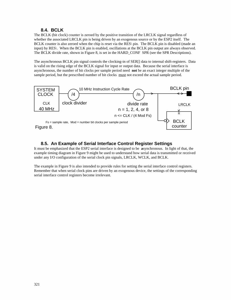
8.4. BCLK The BCLK (bit clock) counter is zeroed by the positive transition of the LRCLK signal regardless of whether the associated LRCLK pin is being driven by an exogenous source or by the ESP2 itself. The BCLK counter is also zeroed when the chip is reset via the RES\ pin. The BCLK pin is disabled (made an input) by RES\. When the BCLK pin is enabled, oscillations at the BCLK pin output are always observed. The BCLK divide rate, shown in Figure 8, is set in the HARD_CONF SPR (see the SPR Descriptions). The asynchronous BCLK pin signal controls the clocking-in of SER[] data to internal shift-registers. Data is valid on the rising edge of the BCLK signal for input or output data. Because the serial interface is asynchronous, the number of bit clocks per sample period need not be an exact integer multiple of the sample period, but the prescribed number of bit clocks must not exceed the actual sample period.
SYSTEM CLOCK
40 MHz
/410 MHz Instruction Cycle Rate
/n
n = 1, 2, 4, or 8
counter
BCLK pin
Figure 8.
clock divider divide rate
BCLK
R
LRCLK
n <= CLK / (4 Mod Fs)
CLK
Fs = sample rate, Mod = number bit clocks per sample period
8.5. An Example of Serial Interface Control Register Settings
It must be emphasized that the ESP2 serial interface is designed to be asynchronous. In light of that, the example timing diagram in Figure 9 might be used to understand how serial data is transmitted or received under any I/O configuration of the serial clock pin signals, LRCLK, WCLK, and BCLK. The example in Figure 9 is also intended to provide rules for setting the serial interface control registers. Remember that when serial clock pins are driven by an exogenous device, the settings of the corresponding serial interface control registers become irrelevant.
321
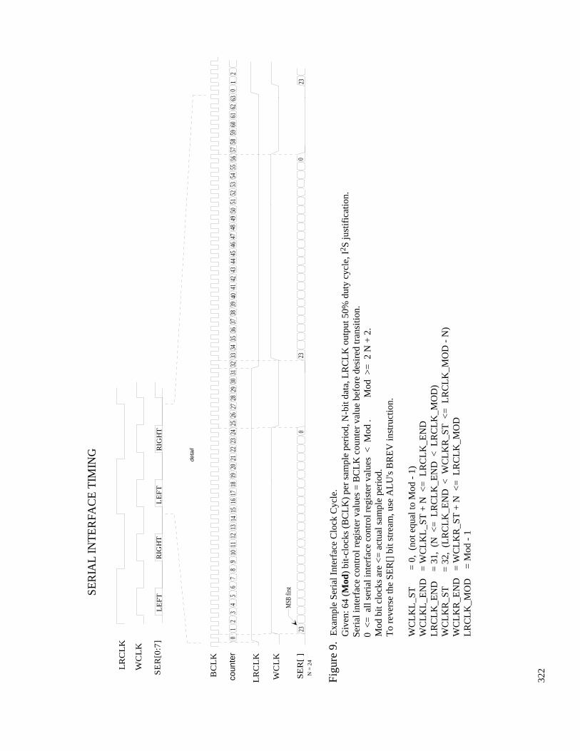
LR
CL
K
SE
R[0
:7]
LE
FT
LE
FT
RIG
HT
RIG
HT
BC
LK
LR
CL
K
WC
LK
SE
RIA
L IN
TE
RFA
CE
TIM
ING
SE
R[
]N
= 2
4
WC
LK
01
23
1617
1819
2021
2223
3132
3324
2526
2728
45
67
89
1011
1213
1415
2930
3435
3637
3839
4041
4243
4445
4647
4849
5051
5253
5455
5657
5859
6061
6263
01
2
deta
il
coun
ter
230
2323
0
MSB
first
F
igur
e 9.
Exa
mpl
e S
eria
l Int
erfa
ce C
lock
Cyc
le.
G
iven
: 64
(Mod
) bi
t-cl
ocks
(B
CL
K)
per
sam
ple
peri
od, N
-bit
data
, LR
CL
K o
utpu
t 50%
dut
y cy
cle,
I2 S
just
ific
atio
n.
Ser
ial i
nter
face
con
trol
reg
iste
r va
lues
= B
CL
K c
ount
er v
alue
bef
ore
desi
red
tran
siti
on.
0 <
= a
ll s
eria
l int
erfa
ce c
ontr
ol r
egis
ter
valu
es <
Mod
.
Mod
>=
2 N
+ 2
.
M
od b
it cl
ocks
are
<=
act
ual s
ampl
e pe
riod
.
T
o re
vers
e th
e S
ER
[] b
it s
trea
m, u
se A
LU
's B
RE
V in
stru
ctio
n.
WC
LK
L_S
T
=
0,
(not
equ
al to
Mod
- 1
)
W
CL
KL
_EN
D
= W
CL
KL
_ST
+ N
<=
LR
CL
K_E
ND
L
RC
LK
_EN
D
= 3
1, (
N <
= L
RC
LK
_EN
D <
LR
CL
K_M
OD
)
W
CL
KR
_ST
= 3
2, (
LR
CL
K_E
ND
< W
CL
KR
_ST
<=
LR
CL
K_M
OD
- N
)
W
CL
KR
_EN
D
= W
CL
KR
_ST
+ N
<=
LR
CL
K_M
OD
L
RC
LK
_MO
D
= M
od -
1
32
2

8.6. Serial Interface Rules - It is recommended that SER data access not be programmed on the queued instruction line following a BIOZ instruction. This is because the IOZ input pin is often connected to the signal LRCLK which latches the SER data SPRs. The queued instruction line following BIOZ is executed prior to suspension; this means that a SER access there might get old data. - It is further recommended that all SER data access occur near the top of the program. The synchronization instruction, BIOZ, allows program main loops to occasionally exceed the sample period. SER data access at the end of a main loop might miss the launch window under that circumstance. - Serial data is always left-justified within 24-bit SER data SPRs. - The WCLK signal always frames the SER[] data. The ESP2 always requires the WCLK signal, either from an exogenous source or self-generated. - In general, the transitions of LRCLK, WCLK, the BCLK counter, and SER[] data all occur on the negative transition of BCLK. Each SER[] data bit is latched on the positive transition of BCLK. - If the serial interface control registers are set up for an N-bit transmission or reception frame, then 24-N LSBs of the SER data SPRs will be transmitted or received as logical zero regardless of their actual value.
8.7. Serial Reset and Synchronization In revision three of the chip, two bits are added to the hard_conf register. These bits are the SERIAL_RESET, and SERIAL_SYNC bits. The bits are added to facilitate the initialization and synchronization of the two independent timing generators when either one or both are driven by the ESP2. The SERIAL_RESET bit can be set to put the serial timing generator into a known state in the event when the serial timing control registers are modified. When this pin is set, the bit clock counters are reset to 0 and the clocks signals are driven in the corresponding state, LRCLK[0:1] = 1, WCLK[0:1] = 0. The BCLK[0:1] pins are also held low. Once the bit is cleared, normal functionality is resumed. This bit can be very useful for production testing of the chip. The SERIAL_SYNC bit can be used to synchronize serial timing generator 1 to the low to high transition of serial timing generator 0. This is very useful in the event that timing generator 1 is running at a multiple of timing generator 0's rate, especially if timing generator 0 is driven from an external source. Whenever it is desired that one timing generator run at a multiple of the base sample rate, timing generator 0 should be set to the base sample rate, timing generator 1 should be set to the multiple rate, and the SERIAL_SYNC bit should be set to synchronize the two generators.
323

9. Halt and Suspension States
9.1. Halting the Chip The chip can be halted unconditionally by writing the HOST_HALT bit of the HOST_CNTL interface register. The HOST_CNTL interface register is accessible directly from the system host, and is also accessible (in a limited way) to the ALU and MAC unit as an SPR (HOST_CNTL_SPR). A mechanism for host-supervised halting under ESP2 program control exists through the HALT pseudo instruction of the ALU. That instruction is used to set the ESP_HALT bit in HOST_CNTL_SPR. If the ESP_HALT_EN bit (located in the HOST_CNTL interface register) is set by the system host, the chip will enter into a halt state when a HALT pseudo is encountered. If the ESP_HALT_EN bit is low, then the ESP_HALT bit is ignored. Program debugging is facilitated by placing HALT pseudo instructions throughout a program as breakpoints. The breakpoints can be activated by the host setting the ESP_HALT_EN bit, or they can be deactivated to allow continuous execution of the program. Recall from the ALU's HALT pseudo instruction description that there is a 1 instruction cycle latency in the execution of the HALT. This results in the execution of the queued instruction line following HALT before the chip enters into the halt state. The chip can be taken out of the halt state by having the host clear the ESP_HALT and HOST_HALT bits of the HOST_CNTL interface register. At run-time, when the IOZ_EN bit of the HOST_CNTL interface register is high, the BIOZ instruction typically causes some amount of time spent in suspension depending upon the program's length with respect to the presumably longer sample period. A less obvious method for 'halting' the chip, then, is to bring the IOZ_EN bit low. By doing so, the host disables ESP2's observation of IOZ input pin activity subsequent to this IOZ_EN event, hence suspending program execution indefinitely after a BIOZ instruction is encountered. This indefinite suspension occurs after a BIOZ instruction because the IOZ status bit in the CCR will never transit high, when the enable bit IOZ_EN is low, to allow the program to resume. (The actual suspension takes place after either the first or second BIOZ instruction following the event, depending upon
whether the IOZ status bit was already set at the time of the event.) The chip can be taken out of an indefinite suspension by having the host set the IOZ_EN bit of the HOST_CNTL interface register.
9.2. Chip State during Halt and Suspension To preserve the state of the chip during a halt or BIOZ suspension, the MAC unit, ALU, and AGEN must perform operations which are nondestructive to the state of GPRs, SPRs, and AORs. As long as the INST_REF_DIS bit of the HARD_CONF SPR is not asserted, micro-instructions will always be refreshed regardless of whether the chip is in a halt/suspension state. The SPRs are fabricated using static memory, so refresh is not an issue there. The GPRs and AORs, however, are fabricated using dynamic memory, so refresh of those registers must be considered. While halted or suspended the PC is frozen, therefore execution will resume at the next unexecuted instruction line in the queue. The HALT_JUMP bit, in the HOST_CNTL interface register and in HOST_CNTL_SPR, monitors the enforcement of normal run-time latency when the ALU instruction queued for execution following halt/suspension (HALT (ESP_HALT), HOST_HALT, or BIOZ) is from the JMP class (Jcc, JScc, RScc). In these cases this HALT_JUMP monitor bit will go high. When the program resumes, HALT_JUMP will automatically clear. While the chip is halted or indefinitely suspended, the PC may be loaded via the standard host/ESP2-register interface for the purpose of vectoring the program coming out of halt/suspension. If the PC is loaded via the interface at this time, the HALT_JUMP bit is automatically cleared.
324

System host loading of the PC does not take the chip out of the halt nor the suspension states. It is not recommended to load the PC from the host interface at run-time because the results are indeterminate. It is neither recommended to load the PC from the host interface during suspension unless the suspension is indefinite. The MAC unit executes its NOP or RFSH pseudo instruction based on the HALT_MAC_REF bit of the HARD_CONF SPR (0 or 1 respectively). Only when the MAC unit executes NOPs is the state of MACRL (the low 24 bits of the 48-bit MAC unit result) preserved; when the MAC unit executes RFSH, MACRL is destroyed. It is not critical during halt or suspension for the MAC unit to be involved with internal register refresh. The ALU executes either a HOST instruction or a HOSTNORFSH pseudo instruction based on the state of the HALT_REF_DIS bit in the HARD_CONF SPR (0 or 1 respectively). Both of these instructions allow host access to internal registers during halt or suspension. HOST provides internal register refresh when no access is pending. The assertion of HALT_REF_DIS disables internal register refresh and always overrides HALT_MAC_REF. (This is not desirable.) The AGEN executes its NOP instruction which tristates the external memory buss and the pin signal, MR/W\ . Refresh of external DRAM occurs if the XMREF_DIS bit in the HARD_CONF SPR is low.
HOST_HALT
ESP_HALT_EN
ESP_HALT
Figure 10
halt state
QD R5V
'74Q_
S
SINGLE_STEP
host reset
host set
BIOZ bit
suspension state
host load PC
Jcc
JSccRScc
JMP-classbranch pending
HALT_JUMP b
PC frozen
instruction cycle
325

9.3. Single Step Mode A program debugging tool exists which allows Single Stepping of programs. When the SINGLE_STEP bit of the HOST_CNTL interface register is set, the ESP2 will execute the next queued single instruction line and then enter a halt state by setting the HOST_HALT bit of the HOST_CNTL register. The host must then clear the HOST_HALT bit in order to have the chip execute the next queued instruction line. Single Stepping can yield erroneous results since the normal inter-unit latencies will disappear. The disappearance of latency warrants consideration of the impact upon all latent instructions: Normal run-time instruction cycle execution latency of the JMP class (Jcc, JScc, RScc) instructions allows the next queued instruction line to be executed prior to the actual branch. The HALT_JUMP bit of HOST_CNTL_SPR and the HOST_CNTL interface register comes into play here monitoring the enforcement of normal run-time execution latency during Single Step. So, there is no difference in the behavior of JMP class instructions during Single Step. Recall that normal run-time execution latency of BIOZ (or BIOZNORFSH) and HALT dictates that the following queued instruction line execute prior to suspension or halt. During Single Step, the instruction cycle execution latency of BIOZ will disappear. This means that the instruction line queued for execution following BIOZ will not execute prior to suspension. In other words, if suspension occurs, the PC will stay frozen for subsequent Steps at the location of the first instruction line queued following BIOZ. When suspension terminates, the program proceeds from that location. This is in opposition to the normal run-time execution latency of BIOZ where the PC becomes frozen at the second queued line during suspension. The same considerations apply to the HALT pseudo. There will be a problem if the Single Step encounters a REPT instruction of the second form having a one-line loop. See the section on Latent Instructions for more.
9.4. Single Pass Operation
An extremely useful tool for ESP2 program debugging is Single Pass execution. 'Single Pass' refers to all those instructions that would normally execute during one sample period. This method of debug is recommended in preference to the Single Step mode. Single Pass can be accomplished quite easily using the IOZ status and IOZ_EN bits of the HOST_CNTL interface register. Assuming that the program has a BIOZ instruction for maintaining sample rate synchronization, the chip can be made to perform a Single Pass by holding the IOZ_EN bit low. When this bit is cleared, the ESP2 will ignore subsequent activity on the IOZ input pin. Therefore, after the BIOZ instruction is executed, ESP2 will remain in a suspension state indefinitely. The host can then set the IOZ status bit of the HOST_CNTL interface register, which has the same effect as a low to high transition at the IOZ input pin, which will cause the program to resume execution. The IOZ status bit will then be automatically cleared by the ESP2 so that the chip will again enter and remain in suspension the next time the BIOZ instruction is reached. The chip is taken out of suspension by a high IOZ status bit in the HOST_CNTL interface register.
326
10. Chip Reset, Initialization, and Synchronization
10.1. Reset The chip has a reset pin (RES\) used for power-up initialization of the chip. Reset will have the following effects on the chip state: 1. The HOST_CNTL interface register and HOST_CNTL_SPR are set to $04 (chip halted). This action clears the IOZ status bit, the BIOZ bit, and the IOZ_EN bit. 2. HARD_CONF SPR is reset to zero to: 1) make all serial interface clock pins (LRCLK[0:1], BCLK[0:1], and WCLK[0:1]) go into high impedance input mode, set BCLK divide rates to /2, 2) enable instruction refresh, and enable GPR/AOR refresh from the ALU only, 3) select linear (SRAM) addressing mode, and disable magnitude truncation to external memory, 4) CAS\ before RAS\ external memory refresh enabled. 5) The OFLAG pin is tristated to be compatible with pre revision 3 chips. 6) SERIAL_RESET and SERIAL_SYNC are off (low) to be compatible with pre-revision 3 chips. 3. External memory buss (address and data) and pin signal, MR/W\, enter tristate. 4. SER_CONF SPR, all bits set to logical 1. This places all SER[0:7] lines in the high impedance
(input) state, and selects timing-set number 1 for all. 5. Serial interface control's BCLK counters reset. 6. The HOST_GPR_PEND bit of the HOST_GPR_CNTL interface register, and the
HOST_INST_PEND bit of the HOST_INST_CNTL interface register are cleared. 7. The PC is cleared. 8. The internal clock divider (/4 in Figure 8) circuit is initialized on the low to high transition of RES\.
This allows synchronization to tester hardware for manufacturer chip debug. 9. The REPT_CNT SPR is cleared.
327

10.2. Initialization Some SPRs may require initialization, while others power-up in unknown states. All
SPR/GPR/AOR initialization can be done in the ESP2 program declarations; this is the recommended way although the system host could also initialize the same registers. SPRs associated with the internal memory refresh mechanism (REFPT, REF, or REFINST) need not be initialized, except for manufacturer test purposes.
1)SER0L, SER0R, SER1L, ..., SER7R Clear the serial data registers being used. 2)SCLK0_REG0,1, SCLK1_REG0,1 Settings of various serial interface clock timings. These registers require initialization only if any of
the serial clock pins will be activated. 3)SER_CONF Configures serial interface data lines, direction and timing set association. 4)HARD_CONF Configures serial interface clock pins (activation and BCLK divide rate), external memory type and
truncation, and internal/external refresh modes. When changing serial pins from input to output at initialization (SER_CONF SPR), it is recommended that LRCLK and BCLK first be activated with WCLK held low. This ensures that the cleared data in the SER0L, SER0R, ..., SER7R SPRs is transferred into the output buffers at the low to high transition of LRCLK before the contents of the buffers is output onto the serial pins during WCLK high time. WCLK can be held low by setting the WCLK_ST and WCLK_END values greater than the LRCLK_MOD value (SCLK0_REG0,1 SCLK1_REG0,1 SPRs) and enabling the word clock output pins (HARD_CONF SPR). Once a couple of sample periods have passed, WCLK can be programmed for normal operation. SERIAL_RESET, and SERIAL_SYNC can be used to synchronize the start of serial timing generators.
5)REPT_CNT This SPR must forever be initialized to zero or bad stuff will happen (JonD). Whenever a program
is overlaid, started, restarted, etc., the REPT_CNT SPR should be cleared. This is easily accomplished sometimes simply by declaration. REPT_CNT controls the automatic looping mechanism for the REPT instruction, and can become activated even if that instruction is never utilized.
6)PC The Program Counter should be initialized to the desired value by the programmer in the
declarations as any other SPR. The PC is in the zero state at reset (RES\). The PC can be initialized by the system host during halt or indefinite suspension. The PC should not be initialized at run-time by the host because the results are indeterminate. To vector a running program at run-time, see the Applications section.
7)GPR/AOR The programmer must zero all application-critical registers in the declarations. 8)HOST_CNTL host interface register. This control register is customarily initialized from the host side. IOZ_EN is usually set, to activate
observation of the IOZ input pin by the ALU BIOZ instruction. Typically, ESP_HALT_EN is set to allow the ESP2 to exercise the HALT pseudo instruction. ESP_HALT and HOST_HALT are customarily cleared to start the processor.
328

10.3. Synchronization.
In systems using multiple ESP2s it may be necessary to ensure that their internal clock dividers which divide the input clock into the 4 clock instruction cycle are synchronized to one another. This is absolutely necessary if multiple ESP2s are communicating on a common external memory bus. For this reason, the IFLAG and OFLAG pins have dual functionality which can be activated via the SYNC_MODE[1:0] bits of the HARD_CONF register. The following truth table indicates the various configurations of the IFLAG and OFLAG pins.
Table 10. SYNC_MODE bit functionality
sync_mode[1:0] OFLAG pin function IFLAG pin function Description
0 Tristate output IFLAG input Rev 2 compatibility
mode
1 OFLG bit IFLAG input Semaphore mode
2 Sync pulse IFLAG input Sync master mode
3 Sync pulse Sync input Sync slave mode As discussed in the previous section on reset, the HARD_CONF is cleared by the RESB pin. This places the IFLAG into standard input mode, and tristates the OFLAG for backward compatibility with earlier versions of the chip. Once the chip has been reset, the functions of these pins can be changed in order to synchronize multiple ESP2s. For this to be accomplished, one ESP2 will serve as the sync master and the remainder will serve as sync slaves. The SYNC_MODE bits of HARD_CONF register of the master are set to 2. This will cause a sync pulse to be output on the OFLAG pin. The SYNC_MODE bits of the slaves are set to 3 which will cause them to synchronize their internal divider to transitions on their IFLAG pin. By wiring the OFLAG pin of the master to the IFLAG pin of the slave, and programming the registers as mentioned, synchronization can be accomplished. The registers should be held in the above states for a minimum of 2 to 3 instructions cycles after which, the SYNC_MODE pins can be changed to other modes. When taking the chips out of synchronization mode, it is suggested that all slaves be switched from mode 3 to either modes 0 or 1, before the master is switched out of mode 2. Since mode 3 synchronizes to transitions on the IFLAG and also outputs a sync pulse matching the state of its internal divider, daisy chaining of ESP2s together is also possible. The intent is to accomodate synchronization in whatever wiring configuration is deemed to be most useful for semaphore communication using IFLAG and OFLAG under normal operating conditions. In daisy chaining configurations where one slave will sync to the master and then pass a corrected sync pulse to the next slave, more that 2 to 3 instruction cycles may be necessary to ensure that the whole chain has locked to the master. As a rule of them, 2 to 3 cycles per link in the chain is probably sufficient.
329

11. Special Purpose Registers All SPRs are read-writable unless specified otherwise. All registers less than 24 bits in width are right justified having the unused bits read as zero. Reading a 'reserved' register returns unspecified data. Following is a map of all the SPRs: Address SPR Name Width Register Purpose $3ff ZERO 24 Zero Constant. Read-only. $3fe REFINST 10 Instruction Refresh counter $3fd REFPT 10 GPR and AOR Refresh Pointer. $3f1 REF n/a Indirect refresh address via refresh counter REFPT $3fc INDIRA 10 Indirect address pointer, A source operand $3fb INDIRB 10 Indirect address pointer, B source operand $3fa INDIRC 10 Indirect address pointer, C destination operand $3c7 INDIRD 10 Indirect address pointer, D source operand $3c6 INDIRE 10 Indirect address pointer, E source operand $3c5 INDIRF 10 Indirect address pointer, F destination operand $3c4 INDIRG 10 Indirect offset pointer, AGEN G-operand $3f9 INDIRECT n/a Indirect address mode $3f8 INDIRINC n/a Indirect address mode with post-increment $3f0 INDIRDEC n/a Indirect address mode with post-decrement $3f7 SCLK0_REG0 24 Serial interface control registers combined to define
set 0 left channel timing and LRCLK0 end. bits:
23:16 15:8 7:0
LRCLK_END0 WCLKL_END0 WCLKL_ST0
$3f6 SCLK0_REG1 24 Serial interface control registers combined to define set 0 right channel timing and BCLK0 modulus-1.
bits: 23:16 15:8 7:0
LRCLK_MOD0 WCLKR_END0 WCLKR_ST0
$3f5 SCLK1_REG0 24 Serial interface control registers combined to define set 1 left channel timing and LRCLK1 end.
bits: 23:16 15:8 7:0
LRCLK_END1 WCLKL_END1 WCLKL_ST1
$3f4 SCLK1_REG1 24 Serial interface control registers combined to define set 1 right channel timing and BCLK1 modulus-1.
bits: 23:16 15:8 7:0
LRCLK_MOD1 WCLKR_END1 WCLKR_ST1
330

$3f3 HARD_CONF 18 Hardware Configuration
bit: 1:0 2 3 4 6:5 7 8 9 10 11 12 13 14 15 16 17 18 19 20 21 22 23
BCLK0 divide rate BCLK0 enable (I/O, 0/1) WCLK0 enable (I/O, 0/1) LRCLK0 enable (I/O, 0/1) BCLK1 divide rate BCLK1 enable (I/O, 0/1) WCLK1 enable (I/O, 0/1) LRCLK1 enable (I/O, 0/1) MUX_ADDR (high active) MAG_TRUNC (high active) TRUNC_WIDTH (high = 24-bit, low=16-bit) HALT_REF_DIS (high active) INST_REF_DIS (high active) HALT_MAC_REF (high active) XMREF_DIS (high active) XMREF_CASDIS (high active) SERIAL_RESET (high active) SERIAL_SYNC (high active) reserved SYNC_MODE[0] SYNC_MODE[1] OFLG bit
$3f2 SER_CONF 16 Serial Data Line Configuration
bit: 0 1 2 3 4 5 6 7 8 9 10 11 12 13 14 15
(logical 0 = timing set number zero) data line 0 timing select data line 1 timing select data line 2 timing select data line 3 timing select data line 4 timing select data line 5 timing select data line 6 timing select data line 7 timing select data line 0 direction (0 = output) data line 1 direction data line 2 direction data line 3 direction data line 4 direction data line 5 direction data line 6 direction data line 7 direction
$3ef SER0L 24 Serial data line zero left channel (SER data SPR) $3ee SER0R 24 Serial data line zero right channel $3ed SER1L 24 Serial data line one left channel
331

$3ec SER1R 24 Serial data line one right channel $3eb SER2L 24 Serial data line two left channel $3ea SER2R 24 Serial data line two right channel $3e9 SER3L 24 Serial data line three left channel $3e8 SER3R 24 Serial data line three right channel $3e7 SER4L 24 Serial data line four left channel $3e6 SER4R 24 Serial data line four right channel $3e5 SER5L 24 Serial data line five left channel $3e4 SER5R 24 Serial data line five right channel $3e3 SER6L 24 Serial data line six left channel $3e2 SER6R 24 Serial data line six right channel $3e1 SER7L 24 Serial data line seven left channel $3e0 SER7R 24 Serial data line seven right channel $3df BASEI 24 Region I base $3de SIZEM1I 24 Region I size less 1 $3dd ENDI 24 Region I end $3dc BASEP 24 Region P base $3db SIZEM1P 24 Region P size less 1 $3da ENDP 24 Region P end $3d9 BASEQ 24 Region Q base $3d8 SIZEM1Q 24 Region Q size less 1 $3d7 ENDQ 24 Region Q end $3d6 BASER 24 Region R base $3d5 SIZEM1R 24 Region R size less 1 $3d4 ENDR 24 Region R end $3d3 BASES 24 Region S base $3d2 SIZEM1S 24 Region S size less 1 $3d1 ENDS 24 Region S end $3d0 BASET 24 Region T base $3cf SIZEM1T 24 Region T size less 1 $3ce ENDT 24 Region T end $3cd BASEU 24 Region U base $3cc SIZEM1U 24 Region U size less 1 $3cb ENDU 24 Region U end $3ca BASEV 24 Region V base $3c9 SIZEM1V 24 Region V size less 1 $3c8 ENDV 24 Region V end $1ff DIL0 24 Data Input Latch SPR $1fe DIL1 24 Data Input Latch SPR $1fd DIL2 24 Data Input Latch SPR $1fc DIL3 24 Data Input Latch SPR $1fb DIL4 24 Data Input Latch SPR $1fa DIL5 24 Data Input Latch SPR $1f9 DIL6 24 Data Input Latch SPR $1f8 DIL7 24 Data Input Latch SPR $1f7 DIL8 24 Data Input Latch SPR $1f6 DIL9 24 Data Input Latch SPR $1f5 DILA 24 Data Input Latch SPR $1f4 DILB 24 Data Input Latch SPR $1f3 DILC 24 Data Input Latch SPR $1f2 DILD 24 Data Input Latch SPR $1f1 DILE 24 Data Input Latch SPR $1f0 DILF 24 Data Input Latch SPR $1ef DOL0 24 Data Output Latch SPR
332

$1ee DOL1 24 Data Output Latch SPR $1ed DOL2 24 Data Output Latch SPR $1ec DOL3 24 Data Output Latch SPR $1eb DOL4 24 Data Output Latch SPR $1ea DOL5 24 Data Output Latch SPR $1e9 DOL6 24 Data Output Latch SPR $1e8 DOL7 24 Data Output Latch SPR $1e7 DOL8 24 Data Output Latch SPR $1e6 DOL9 24 Data Output Latch SPR $1e5 DOLA 24 Data Output Latch SPR $1e4 DOLB 24 Data Output Latch SPR $1e3 DOLC 24 Data Output Latch SPR $1e2 DOLD 24 Data Output Latch SPR $1e1 DOLE 24 Data Output Latch SPR $1e0 DOLF 24 Data Output Latch SPR $1df CCR 9 Condition Code Register
bit: 0 1 2 3 4 5 6 7 8
Zero flag Less Than flag oVerflow flag Carry flag Negative flag A operand Negative flag B operand Negative flag IFLG (read-only) IOZ status bit (read-only)
$1de CMR 10 Condition Mask Register
bit: 0 1 2 3 4 5 6 7 8 9
Zero mask Less Than mask oVerflow mask Carry mask Negative mask A operand Negative mask B operand Negative mask IFLG mask IOZ mask NOT bit
$1dd PC 10 Program Counter (writable with caveat) $1dc PCSTACK0 10 PC stack, top $1db PCSTACK1 10 PC stack, 1 below top $1da PCSTACK2 10 PC stack, 2 below top $1d9 PCSTACK3 10 PC stack, 3 below top (bottom). $1d8 REPT_ST 10 Holds PC value for start of repeat block $1d7 REPT_END 10 Holds PC value for end of repeat block. $1d6 REPT_CNT 24 Repeat counter for REPT instruction. $1d5 ALU_SHIFT 24 ALU shift amount (only the five LSBs are used to control
double precision shifts in the ALU).
333
$1d4 MACRL 24 MAC Result Low latch (read-only) $1d3 MACP_H 24 MACP latch high word (write-only) $1d3 MACH 24 MAC latch high word (read-only) $1d2 MACP_HC 24 MACP latch high word - clear low word
(write-only) $1d1 MACP_L 24 MACP latch low word (write-only) $1d1 MACL 24 MAC latch low word (read-only) $1d0 MACP_LS 24 MACP latch low word - sign extend into high word
(write-only) $1cf HOST_GPR_DATA 24 GPR/SPR/AOR data access by host $1ce HOST_CNTL_SPR 8 Image of the HOST_CNTL host interface register for
internal access to status and control bits. All high active.
bit: 0 1 2 3 4 5 6 7
ESP_HALT_EN (read-only) ESP_HALT HOST_HALT (read-only) IOZ status bit IOZ_EN (read-only) BIOZ bit (read-only) SINGLE_STEP (read-only) HALT_JUMP (read-only)
$1cd HALF 24 Read-only constant register containing the hex value $400000. This value is necessary for some MAC unit pseudo instructions.
$1cc ONE 24 Read-only constant register containing the hex value $000001.
$1cb MINUS1 24 Read-only constant register containing the hex value $800000.
$1ca n/a reserved address available for future use $1c9 n/a reserved (tied in with $1c8 since HOST_ESP_FACE is
accessed over the GPR busses which accesses two registers at a time and column multiplexes the busses).
$1c8 HOST_ESP_FACE 24 SPR mapping of the HOST_ESP_FACE_B2,1,0 host interface registers. This register is uncommitted.
334
11.1 SPR Descriptions ALU_SHIFT is an SPR which supplies a shift amount (an extra source operand) to the ALU during the execution of the ASDH, ASDL, LSDH, and LSDL instructions. Regarding its availability to the ALU for its prescribed purpose, loading ALU_SHIFT follows the same inter-unit latency rules as any other GPR/AOR destination. ALU_SHIFT is read/writable and could be used like a GPR in programs where the double precision shift instructions are not required. BASE, END, and SIZEM1 registers are used by the Address Generator for accessing up to eight regions in external memory. Each of the regions has a programmable size and location in physical memory. See the AGEN description for further information. CCR and CMR are the Condition Code and Condition Mask Register and are concerned with conditional execution of instructions. The CCR is set automatically only in the ALU. These two SPRs are readable and writable with the exception of the IOZ status bit and IFLG which are read-only in the CCR. For further information see the description of the Conditional Execution Mechanism in the section on the Condition Code Register. The DIL and DOL registers are the data interface to external memory. Data coming into the chip is latched in the designated DIL register. Data to be written by the chip must be placed in one of the DOL registers. These SPRs are readable and writable like GPRs. See the sections on the External Memory Interface for more information on the use of these registers. The HALF register is a read-only constant containing the value $400000. This value is necessary for some MAC unit pseudo instructions and has therefore been hardwired into an SPR. The HARD_CONF register is an 18-bit SPR used to configure multifarious aspects of the chip hardware. Upon reset, this register will initialize to 0. The LSBs of HARD_CONF determine whether each serial clock pin acts as input or output, and determine the divide-down rates of BCLK0 and BCLK1 (00 corresponds to /2, 01 <=> /4, 10 <=> /8, 11 <=> /1). When the individual serial clock pins are not enabled, they are in the high impedance input mode. The MUX_ADDR, MAG_TRUNC, and TRUNC_WIDTH bits are readable and writable in this register. When the MUX_ADDR bit is low, this yields the linear external addressing mode suitable for SRAM or peripheral I/O. When MUX_ADDR is high, multiplexed addressing suitable for DRAM is activated. Assertion of MAG_TRUNC invokes the magnitude truncation mode of WR to external memory. TRUNC_WIDTH low selects magnitude truncation to 16 bits, high selects to 24 bits. The INST_REF_DIS (instruction refresh disable), HALT_REF_DIS (halt refresh disable), and HALT_MAC_REF (halt MAC unit refresh) bits are useful for controlling the automatic refresh of instructions and internal registers. See the section on Internal Memory Refresh for details. The XMREF_DIS (external memory refresh disable) and XMREF_CASDIS (external memory refresh CAS\ disable) bits control the refresh mode of external memory. The default mode provides CAS\ before RAS\ refresh. Setting XMREF_CASDIS provides RAS\-only refresh. Setting XMREF_DIS disables external memory refresh altogether regardless of the setting of XMREF_CASDIS. Setting the SERIAL_RESET bit will keep the serial clocks in a reset state in which both WCLK pins are low, both LRCLK pins are high, and both BCLK pins are low. This can be useful for resetting the clocks after changing registers that control the period and duty cycle of the WCLK and LRCLK pins. Setting SERIAL_SYNC causes serial timing generator 1 to reset on the low to high transition of LRCLK[0] as well as LRCLK[1]. This can be useful for synchronizing the two timing generators when timing generator 1 is running at an integer multiple of the sample rate set by timing generator 0.
335

SYNC_MODE[1:0] and OFLG are used in conjunction with the OFLAG and IFLAG pins to provide instuctions synchronization between multiple ESP2s. (See the section on synchronization for a description of the function of these bits). HOST_CNTL_SPR is an SPR image of the HOST_CNTL host interface register. All of the bits of this register can be read by the ESP2 program to allow access to these hardware status and control bits. For a description of this register refer to the section on Halting the Chip; also the description of the HOST_CNTL interface register.
The ESP_HALT bit can be written. This is necessary for the proper execution of the HALT pseudo instruction in the ALU.
The IOZ status bit appears in the CCR and can easily be polled. Detecting and clearing a set IOZ status bit can be accomplished automatically by executing the BIOZ instruction. Alternately, the IOZ status bit can be written via this SPR to allow manual program control. The HOST_ESP_FACE register is a concatenation of three 8-bit host interface registers which are made accessible as an SPR to ESP2 instructions. Like HOST_GPR_DATA, this SPR is unusual in the respect that it is directly accessible from both the host interface and the ESP2 without the need to execute HOST or BIOZ instructions. What differentiates HOST_ESP_FACE from HOST_GPR_DATA is that it is uncommitted; meaning, the programmer is free to utilize this resource in any opportune manner. Since one of the purposes of the host interface is host access of GPRs/AORs/SPRs, this register could be accessed like any other SPR using the mechanism described in the Host/ESP2 Interface description. But this is an idiosyncrasy of the design which is not the intended use of this register. One possible use of HOST_ESP_FACE would be in a DMA (direct memory access) scheme where the ESP2's external memory were being quickly loaded (or read). This SPR would be written by some exogenous mechanism, then a tight ESP2 loop would write that data out. The IFLAG and OFLAG pins might act as the semaphores in this scheme. The HOST_GPR_DATA register is mapped as an SPR to provide the link from the outside world (the system host) to all the internal ESP2 registers (GPR/SPR/AOR). This register is the 24-bit SPR mapping of the concatenated 8-bit HOST_GPR_DATA_B2,1,0 host interface registers. The ESP2 automatically moves pending host data to and from this SPR during ALU HOST instruction execution. The INDIRA,B,C,D,E,F,G SPRs hold indirect addresses. Writing these SPRs allows modification of the indirect address. See the section on Indirect Register Addressing. The INDIRDEC address is used in the same manner as INDIRECT, but it causes a post-decrement of the corresponding (INDIR) pointer register. The decremented value is ready for the next instruction cycle. If INDIRDEC is used in a skipped instruction, the address will not be decremented. The INDIRECT address is used to initiate indirect addressing. When this address is used as the A operand address, for example, the contents of the INDIRA pointer register is substituted for the address of that operand. The same happens for the remaining operands substituting the INDIRB, INDIRC, INDIRD, INDIRE, INDIRF and INDIRG SPRs, respectively. The INDIRINC address is used in the same manner as INDIRECT, but it causes a post-increment of the corresponding (INDIR) pointer register. The incremented value is ready for the next instruction cycle. If INDIRINC is used in a skipped instruction, the address will not be incremented. MACH and MACL are the most significant and least significant halves of the MAC unit's unsaturated MAC read-only latch. MACP_H and MACP_L are the most significant and least significant halves of the MAC unit's write-only Preload latch. Since these two registers are write-only and the MACH and MACL registers are read-only, they have been mapped to the same addresses.
336

MACP_HC is a secondary method of writing the high word of the MAC Preload latch (MACP) which simultaneously clears the MACP_L register. MACP_LS is a secondary method of writing the low word of the MAC Preload latch (MACP) which simultaneously sign-extends the MSB of the data entering the MACP_L register into the 24-bit MACP_H register. MACRL is the low 24 bits of the MAC unit result after shifting and saturation. The MINUS1 register is a read-only constant containing the value $800000. This value is required by some MAC unit pseudo instructions. The ONE register is a read-only constant containing the value $000001. This value is required by the MAC unit NOP pseudo instruction and has, therefore, been hardwired into an SPR. PC is the Program Counter. This SPR is readable and writable. At run-time there are severe hazards associated with writing to the PC from the host or as destination of the MAC unit or ALU. But the PC can be written by the host with no caveat while the chip is halted or indefinitely suspended, to initialize the start point of a program. The PC is cleared on chip reset. PCSTACK0,1,2,3 compose a four deep stack for keeping track of the PC during subroutine calls. JScc pushes the PC value + 2 onto the top of the stack (PCSTACK0), and RScc pops the new PC value from the top of the stack. REF is a reserved address used during internal register refresh. Specifying this address as a source or destination operand address causes indirect use of the REFPT contents as the operand address. When REF is used as the source and destination operand so as to accomplish refresh, the same contents of REFPT is used for both source and destination. Specifying REF as the source operand of an instruction, REFPT is incremented in preparation for use as a source operand for another refresh operation. The newly incremented value is not available as the destination address until the time at which the current destination address is decoded for the function unit that caused the increment. See section on GPR and AOR Refresh for additional information on the use of these addresses. REFINST is the 10-bit refresh counter for refreshing instructions. See the section on Internal Memory Refresh for more information. REFPT is the 10-bit refresh counter for refreshing internal registers, GPR/AOR. See the section on GPR and AOR Refresh for more information.
337

REPT_ST, REPT_END, and REPT_CNT are used as extra sources by the REPT instruction. When REPT is executed, REPT_ST always gets loaded with the value of the PC for the next instruction line queued for execution. REPT_END always gets loaded with the value from the A operand field of the instruction. REPT_CNT gets loaded with the value from the B operand field or the B operand depending upon the form of the instruction. SCLK0_REG0, SCLK0_REG1, SCLK1_REG0, and SCLK1_REG1 are concatenated registers each containing three 8-bit serial interface control registers used for setting serial clock timings. The SPR map lists the control registers contained within each SPR, while the Serial Interface section describes how those control registers are used. SER0L, SER0R, SER1L, ... Repositories for serial data transmission to and from other ESP2 chips, A/D and D/A converters, and other serial devices. There are 8 serial stereo data lines (physical pins) having a left and right channel-data SPR associated with each. See the section on the Serial Interface. The serial data line configuration register, SER_CONF, is a 16-bit register whose upper byte has one bit for each serial data line, which designates that data line as input or output. A logical 1 in the associated bit indicates that the data line is an input. In the lower byte there is a bit per data line which associates one of two timing sets with that data line: 0 = timing set number 0, 1 = timing set 1. See the SPR map in this section on Special Purpose Registers for the exact definition of bits. ZERO is the constant value $000000 hardwired into the chip. Since this value is required by many of the pseudo instructions, it has been included as an SPR. It is also used as the null destination in cases where the result of an instruction is either undefined or not of interest.
338

12. Host/ESP2 Interface The purpose of the host interface is to access all the ESP2 internal registers and instruction memory. There are separate mechanisms for accessing each which are described herewith. The host interface consists of five address pins HA[4:0], eight data pins HD[7:0], a read/write pin HR/W\, and a chip select pin CS\. HA[4:0] and HR/W\ are latched on the falling edge of CS\. In a read cycle, the ESP2 will assert the HD[7:0] pins with the read-data while CS\ is low. In a write cycle, the HD[7:0] pins will propagate into the addressed register and be latched on the rise of CS\.
CS
Tas Tah Tds Tdh
HA[4:0]
HD[7:0]
Tws Twh
HR/W
Write Cycle Timing
CS
Tas
Tah
Thz
HA[4:0]
HD[7:0]Tws Twh
HR/W
Read Cycle Timing
Tacc
Toe
Figure 11. Tas = Address Setup to CS\ falling edge Tah = Address Hold from CS\ falling edge Tws = HR/W\ Setup to CS\ falling edge Twh = HR/W\ Hold from CS\ falling edge Tds = Data Setup to CS\ rising edge (write cycle) Tdh = Data Hold from CS\ rising edge (write cycle) Toe = CS\ falling edge to Data Active delay (read cycle, output enable) Tacc = CS\ falling edge to Data Valid (read cycle, access time) Thz = CS\ rising edge to Data Tristate (read cycle)
339

12.1. Host/ESP2-Register Interface The HOST_GPR_PEND bit of the HOST_GPR_CNTL host interface register is at once the semaphore and the command to read or write an internal register (GPR/AOR/SPR). When there is no internal register access pending, internal register refresh typically occurs. When the chip is not halted and if an access is pending, data will be automatically moved from/to HOST_GPR_DATA (the SPR image of the HOST_GPR_DATA_B2,1,0 interface registers) to/from an internal register during the first available HOST or BIOZ instruction. In this manner the ALU grants host access along normal ALU data paths. The direction of transfer is specified by the HOST_GPR_RW\ bit of the HOST_GPR_CNTL interface register. Depending on the location and frequency of HOST or BIOZ instructions in the executing program, there is typically some delay before the write to or read of the GPR/AOR/SPR actually takes place. The worst case delay under typical operating conditions is one sample period. When the access has been completed, the HOST_GPR_PEND bit will be cleared. The host will not be forced to hang waiting for the semaphore because the host can poll it. When the chip is halted or indefinitely suspended and an access is pending, the ALU is continuously executing HOST instructions by design. Therefore there is minimum delay for the transfer from/to the HOST_GPR_DATA SPR. Since the system host presumably runs asynchronous to the internal instruction cycle, the HOST_GPR_PEND bit must still be polled.
12.1.1. Writing GPR/AOR/SPR A write of a GPR/AOR/SPR via the host interface involves the following steps: 1. Check the HOST_GPR_PEND bit of the HOST_GPR_CNTL interface register to see that it is low
meaning that there is no register transfer pending. 2. Write three bytes of data to the HOST_GPR_DATA_B2,1,0 interface registers. (If these registers
already hold the desired data because of a previous GPR/AOR/SPR-write, this step can be ignored). 3. Write the GPR/AOR/SPR address to the HOST_GPR_ADDR1,0 interface registers. 4. Write $80 into the HOST_GPR_CNTL interface register initiating the write. The HOST_GPR_PEND
bit when set constitutes the command to write when the HOST_GPR_RW\ bit is low. By observing this bit, the write event can be monitored because the bit goes low when the write occurs. 12.1.2. Reading GPR/AOR/SPR
A read of a GPR/AOR/SPR via the host interface involves the following steps: 1. Check the HOST_GPR_PEND bit of the HOST_GPR_CNTL interface register to see that it is low
meaning that there is no register transfer pending. 2. Write the GPR/AOR/SPR address to the HOST_GPR_ADDR1,0 interface registers. 3. Write $81 to the HOST_GPR_CNTL interface register, setting the HOST_GPR_PEND bit. The
HOST_GPR_PEND bit when set constitutes the command to read when the HOST_GPR_RW\ bit is high.
4. Once the HOST_GPR_PEND bit of the HOST_GPR_CNTL interface register has been
automatically cleared, read three bytes of data from the HOST_GPR_DATA_B2,1,0 interface registers.
340

12.2. Host/ESP2-Instruction Interface The HOST_INST_PEND bit of the HOST_INST_CNTL host interface register is at once the semaphore and the command to read or write one 96-bit instruction. When there is no instruction access pending, instruction refresh typically occurs. Host access to instruction memory is always allowed on every instruction cycle whether or not the chip is halted; there are no hazards. When an access is pending, one instruction will be automatically moved from/to the HOST_INST_DATA_B11,...,0 interface registers along a separate 96-bit wide data path in a direction specified by the HOST_INST_RW\ bit of the HOST_INST_CNTL interface register. When the access has been completed, the HOST_INST_PEND bit will be automatically cleared. The host will not be forced to hang waiting for the semaphore because the host can poll it. Since the system host presumably runs asynchronous to the internal instruction cycle, it is always necessary to poll the HOST_INST_PEND bit.
12.2.1. Writing Instruction Memory
A write of a single instruction via the host interface involves the following steps: 1. Check the HOST_INST_PEND bit of the HOST_INSTR_CNTL interface register to see that it is low
meaning that there is no instruction memory transfer pending. 2. Write twelve bytes of data to the HOST_INST_DATA_B11,...,0 interface registers. (If these registers
already hold the desired data because of a previous instruction-write, this step can be ignored). 3. Write the instruction address to the HOST_INST_ADDR1,0 interface registers. 4. Write $80 to the HOST_INST_CNTL interface register initiating the write. The HOST_INST_PEND
bit when set constitutes the command to write when the HOST_INST_RW\ bit is low. By observing this bit, the write event can be monitored because the bit goes low when the write occurs.
12.2.2. Reading Instruction Memory
A read of a single instruction via the host interface involves the following steps: 1. Check the HOST_INST_PEND bit of the HOST_INST_CNTL interface register to see that it is low
meaning that there is no instruction memory transfer pending. 2. Write the instruction address to the HOST_INST_ADDR1,0 interface registers. 3. Write $81 to the HOST_INST_CNTL interface register, setting the HOST_INST_PEND bit. The
HOST_INST_PEND bit when set constitutes the command to read when the HOST_INST_RW\ bit is high.
4. Once the HOST_INST_PEND bit of the HOST_INST_CNTL interface register has been automatically
cleared, read twelve bytes of data from the HOST_INST_DATA_B11,...,0 interface registers.
341

12.3. Host Interface Registers 'Reserved' registers are nonexistent; reading from them returns unspecified data.
12.3.1. Testing For test purposes, one may be interested in writing then verifying host interface registers to determine whether the ESP2 is alive and powered. The host interface registers are designed to be accessed asynchronously from the system host. This design demands a special procedure for testing some of the host interface registers. The HOST_ESP_FACE_B2,1,0 registers can be tested in a straight-forward manner. When testing HOST_INST_CNTL and HOST_GPR_CNTL, keep in mind that the associated _PEND bit is self-clearing. In halt state, the HOST_GPR_PEND bit clears itself quickly. When testing HOST_INST_DATA_B11,...,0 HOST_INST_ADDR1,0 HOST_GPR_DATA_B2,1,0 HOST_GPR_ADDR1,0 one must employ the following procedure: -Write the desired _INST_ or _GPR_ host interface registers from the list above. -Set the _PEND bit in the HOST_INST_CNTL or the HOST_GPR_CNTL register, respectively. -Wait for the associated _PEND bit to clear, then verify data previously written to the selected host interface registers. Thorough testing of GPRs/AORs, some SPRs, and the instruction (program) memory, themselves, involves the erasure of some hidden internal registers. The correct procedure follows the section Host/ESP2 Interface, with the following augmentation: After the test data is written to some GPR/AOR/SPR or instruction memory, the test data being held in the interface registers must be wiped using different data, and then a write to the read-only SPR called ZERO must occur (it is not sufficient to simply wipe out the host interface register data). Then, the test data can be read back from the memory-under-test and verified.
342

The HOST_CNTL register is tricky to test. /*********************************** test HOST_CNTL register ***********************************/ error1 = error2 = error = 0; /*test the halt bit by itself*/ for(i=0; i<LOOPS; i++) host_inyaface->host_cntl = 0; temp = host_inyaface->host_inst_data_b4; /* electrical flack */ if((host_inyaface->host_cntl & HOST_HALT) != 0) error = 1; host_inyaface->host_cntl = HOST_HALT; temp = host_inyaface->host_inst_data_b5; /* electrical flack */ if((host_inyaface->host_cntl & HOST_HALT) != HOST_HALT) error = 1; mask = 0x7f; /*mask off HALT_JUMP bit*/ logic = 0xd7; temp1 = (0x55 | HOST_HALT) & mask; temp2 = (0xaa | HOST_HALT) & mask; /*test performed in halt mode*/ for(i=0; i<LOOPS; i++) host_inyaface->host_cntl = temp1; temp = host_inyaface->host_inst_data_b2; /* electrical flack */ while((temp = host_inyaface->host_cntl & mask) != temp1) if(error1) break; error1 = 1; printf("\nerror: host_cntl = %02x\n", temp); printf("expected %02x above\n", temp1); printf("For this test to work in Rev 1 or higher, the IOZ pin must be jumpered either to MPU_IOZ or GND\n"); host_inyaface->host_cntl = temp2; temp = host_inyaface->host_inst_data_b3; /* electrical flack */ while((temp = host_inyaface->host_cntl & mask) != (temp2 & logic)) if(error2) break; /*when both IOZ and BIOZ bits are high, they reset themselves. */ error2 = 1; printf("\nerror: host_cntl = %02x\n", temp); printf("expected %02x above\n", temp2 & logic); if(!error1 && !error2 && !error)printf("HOST_CNTL host interface register is good.\n"); else if(error)printf("\nERROR! HOST_CNTL host interface register has faulty HOST_HALT bit.\n"); else if(error1 || error2)printf("\nERROR! HOST_CNTL host interface register is faulty.\n"); /**************************************************************************************/
343
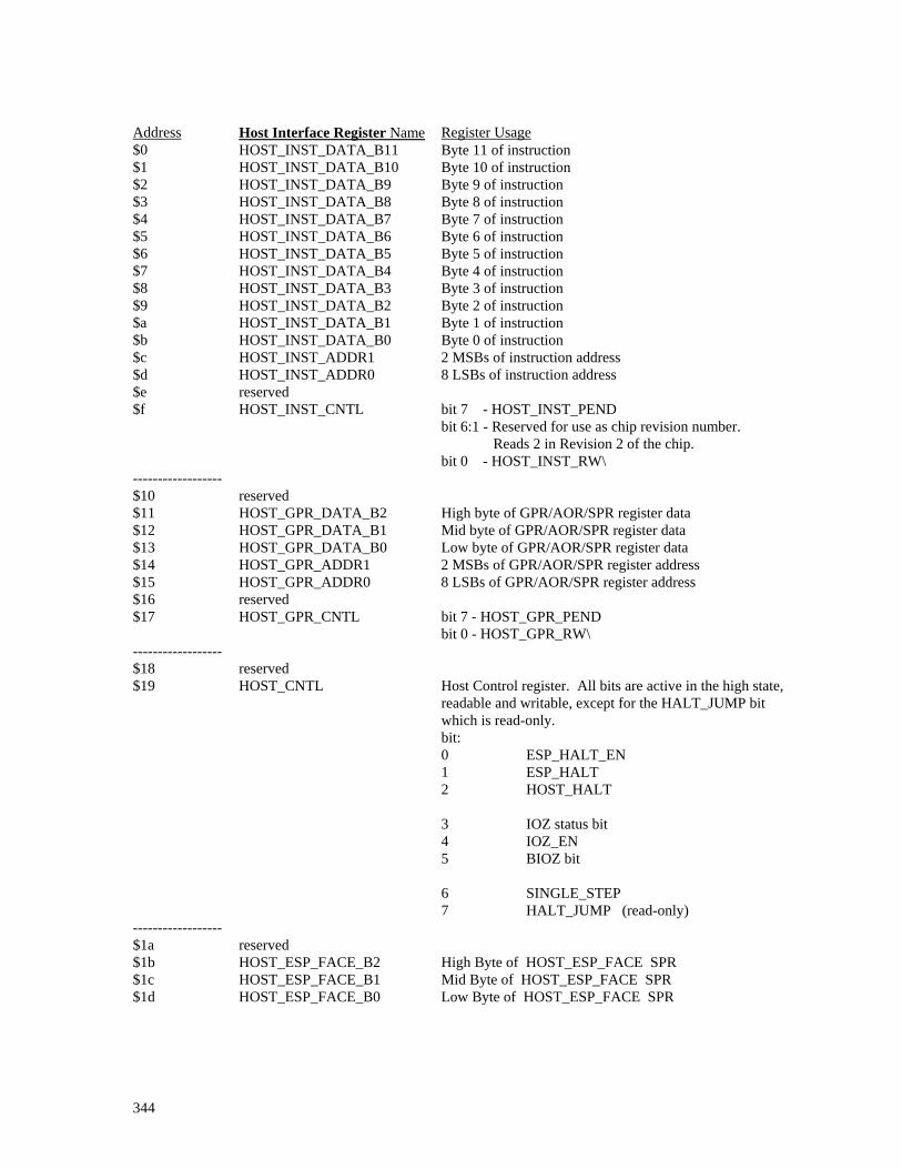
Address Host Interface Register Name Register Usage $0 $1 $2 $3 $4 $5 $6 $7 $8 $9 $a $b
HOST_INST_DATA_B11 HOST_INST_DATA_B10 HOST_INST_DATA_B9 HOST_INST_DATA_B8 HOST_INST_DATA_B7 HOST_INST_DATA_B6 HOST_INST_DATA_B5 HOST_INST_DATA_B4 HOST_INST_DATA_B3 HOST_INST_DATA_B2 HOST_INST_DATA_B1 HOST_INST_DATA_B0
Byte 11 of instruction Byte 10 of instruction Byte 9 of instruction Byte 8 of instruction Byte 7 of instruction Byte 6 of instruction Byte 5 of instruction Byte 4 of instruction Byte 3 of instruction Byte 2 of instruction Byte 1 of instruction Byte 0 of instruction
$c HOST_INST_ADDR1 2 MSBs of instruction address $d HOST_INST_ADDR0 8 LSBs of instruction address $e reserved $f HOST_INST_CNTL bit 7 - HOST_INST_PEND
bit 6:1 - Reserved for use as chip revision number. Reads 2 in Revision 2 of the chip. bit 0 - HOST_INST_RW\
------------------ $10 reserved $11 $12 $13
HOST_GPR_DATA_B2 HOST_GPR_DATA_B1 HOST_GPR_DATA_B0
High byte of GPR/AOR/SPR register data Mid byte of GPR/AOR/SPR register data Low byte of GPR/AOR/SPR register data
$14 HOST_GPR_ADDR1 2 MSBs of GPR/AOR/SPR register address $15 HOST_GPR_ADDR0 8 LSBs of GPR/AOR/SPR register address $16 reserved $17 HOST_GPR_CNTL bit 7 - HOST_GPR_PEND
bit 0 - HOST_GPR_RW\ ------------------ $18 reserved $19 HOST_CNTL Host Control register. All bits are active in the high state,
readable and writable, except for the HALT_JUMP bit which is read-only.
bit: 0 1 2 3 4 5 6 7
ESP_HALT_EN ESP_HALT HOST_HALT IOZ status bit IOZ_EN BIOZ bit SINGLE_STEP HALT_JUMP (read-only)
------------------ $1a reserved $1b HOST_ESP_FACE_B2 High Byte of HOST_ESP_FACE SPR $1c HOST_ESP_FACE_B1 Mid Byte of HOST_ESP_FACE SPR $1d HOST_ESP_FACE_B0 Low Byte of HOST_ESP_FACE SPR
344

12.3.2. Some Host Interface Register Descriptions The host control register, HOST_CNTL, is the only register for controlling the operation of the ESP2 that is directly accessible from the host processor. This read/write host interface register allows the host to recall the hardware status, and provides direct control of the ESP2 regardless of the state of its internal function units. This register is also directly accessible by ESP2 as an SPR in a limited way (refer to the HOST_CNTL_SPR description). The ESP_HALT and ESP_HALT_EN bits in conjunction with the HALT pseudo instruction provide a means of break-pointing during algorithm execution (refer to the section on Halting the Chip). The HOST_HALT bit provides a means of unconditionally halting the ESP2 by the host processor regardless of the state of the internal function units. The BIOZ bit, the IOZ status bit, and the IOZ_EN bit operate in conjunction with the ALU BIOZ instruction and are described in detail in the description of that instruction. The SINGLE_STEP bit provides a mechanism for the successive execution of single queued instruction lines. HALT_JUMP is a read-only monitor-bit. It goes high when the chip enters the halt or suspension state (HALT (ESP_HALT), HOST_HALT, or BIOZ) if the ALU instruction queued for execution is from the JMP class (Jcc, JScc, RScc). When this monitor bit goes high, normal run-time instruction cycle execution latencies are being enforced coming out of halt/suspension. The bit automatically clears when the program resumes. These bits are discussed further in the section on Halt and Suspension States. HOST_ESP_FACE_B2,1,0 are uncommitted host interface registers (mapped into three consecutive bytes from the host side) which are also directly accessible by ESP2 as one (24-bit) SPR called HOST_ESP_FACE. The HOST_GPR_DATA_B2,1,0, HOST_ESP_FACE_B2,1,0, and HOST_CNTL host interface registers are distinguished in so far as they are simultaneously mapped as SPRs, so can therefore be accessed directly by ESP2. This means that there is no need for the execution of BIOZ or HOST instructions in order that the host be able to communicate with a running ESP2 program via these registers; and vice versa. This is advantageous for fast intercommunication. In the host register space, these registers are mapped as consecutive bytes, whereas in the SPR space they are concatenated into single 24-bit registers. See the SPR Descriptions for a bit more about HOST_GPR_DATA_B2,1,0, the internal register link to the outside world.
345

13. Pin List Pin Name Description Function Number External Memory Interface MADDR[23:0] MDATA[23:0] MR/W\ RAS\ CAS\ MEM_REQ\ VSS_A VSS_D VDD_A VDD_D
Address Buss Data Buss Write Enable Row Address Strobe Column Address Strobe Memory Cycle Request Ground to address buffers Ground to data buffers Supply to address buffers Supply to data buffers
Output/Tristate I/O Output/Tristate Output Output I/O Tristate Ground Ground Power Power Subtotal
24 24 1 1 1 1 1 1 1 1 56
Host Interface HA[4:0] HD[7:0] CS\
Host Address Host Data Chip Select (edge sensitive)
Input I/O Input
5 8 1
HR/W\ VSS_H VDD_H
Write Enable Ground to buffers Supply to buffers
Input Ground Power Subtotal
1 1 1 17
Serial Interface BCLK[1:0] Bit Clocks
(edge sensitive) I/O 2
WCLK[1:0] Word Clocks (edge sensitive)
I/O 2
LRCLK[1:0] SER[7:0] VSS_S VDD_S
Left/Right Clocks Serial Data Lines Ground to buffers Supply to buffers
I/O I/O Ground Power Subtotal
2 8 1 1 16
Miscellaneous CLK IOZ
System Clock (four times instruction rate, 40 MHz nominal) Sample Rate Synchronization (rising edge sensitive, refer to BIOZ instruction)
Input Input
1 1
IFLAG OFLAG RES\ VSS[3:0] VDD[1:0]
Input Flag Output Flag Chip Reset Ground to chip internals Supply to chip internals
Input Output/Tristate Input Ground Power Subtotal
1 1 1 4 2 11
Grand total 100
346

Table 11. ESP2 Chip Pinout
PIN NUMBER NAME FUNCTION comment 1 resb Input 2 clk Input 3 iflag Input 4 VSS[0] Ground Connect to VSS frame 5 oflag Output/Tristate 6 VDD_S Power 7 bclk0 I/O 8 wclk0 I/O 9 lrclk0 I/O 10 bclk1 I/O 11 wclk1 I/O 12 lrclk1 I/O 13 ser7 I/O 14 ser6 I/O 15 ser5 I/O 16 ser4 I/O 17 ser3 I/O 18 ser2 I/O 19 ser1 I/O 20 ser0 I/O 21 VSS_S Ground 22 VSS[1] Ground Connect to VSS frame 23 VDD[0] Power 24 VDD_A Power 25 mrwb Output/Tristate 26 maddr[23] Output/Tristate 27 maddr[22] Output/Tristate 28 maddr[21] Output/Tristate 29 maddr[20] Output/Tristate 30 maddr[19] Output/Tristate 31 maddr[18] Output/Tristate 32 maddr[17] Output/Tristate 33 maddr[16] Output/Tristate 34 maddr[15] Output/Tristate 35 maddr[14] Output/Tristate 36 maddr[13] Output/Tristate 37 maddr[12] Output/Tristate 38 maddr[11] Output/Tristate 39 maddr[10] Output/Tristate 40 maddr[9] Output/Tristate 41 maddr[8] Output/Tristate 42 maddr[7] Output/Tristate 43 maddr[6] Output/Tristate 44 maddr[5] Output/Tristate 45 maddr[4] Output/Tristate 46 maddr[3] Output/Tristate 47 maddr[2] Output/Tristate 48 maddr[1] Output/Tristate 49 maddr[0] Output/Tristate 50 VSS_A Ground
347

PIN NUMBER NAME FUNCTION comment 51 VSS_D Ground 52 mdata[23] I/O 53 mdata[22] I/O 54 mdata[21] I/O 55 mdata[20] I/O 56 mdata[19] I/O 57 mdata[18] I/O 58 mdata[17] I/O 59 mdata[16] I/O 60 mdata[15] I/O 61 mdata[14] I/O 62 mdata[13] I/O 63 mdata[12] I/O 64 mdata[11] I/O 65 mdata[10] I/O 66 mdata[9] I/O 67 mdata[8] I/O 68 mdata[7] I/O 69 mdata[6] I/O 70 mdata[5] I/O 71 mdata[4] I/O 72 mdata[3] I/O 73 mdata[2] I/O 74 mdata[1] I/O 75 mdata[0] I/O 76 VDD_D Power 77 rasb Output 78 casb Output 79 mem_reqb I/O 80 ioz Input 81 csb Input 82 hrwb Input 83 VSS[3] Ground Connect to VSS frame 84 VSS[2] Ground Connect to VSS frame 85 VDD[1] Power 86 VDD_H Power 87 ha[4] Input 88 ha[3] Input 89 ha[2] Input 90 ha[1] Input 91 ha[0] Input 92 hd[7] I/O 93 hd[6] I/O 94 hd[5] I/O 95 hd[4] I/O 96 hd[3] I/O 97 hd[2] I/O 98 hd[1] I/O 99 hd[0] I/O 100 VSS_H Ground
348

1 2 3 4 5 6 7 8 9 10 11 12 13 14 15 16 17 18 19 20 21 22 23 24 25
75 74 73 72 71 70 69 68 67 66 65 64 63 62 61 60 59 58 57 56 55 54 53 52 51
26
50
49
48
47
46
45
44
43
42
41
40
39
38
37
36
35
34
33
32
31
30
29
28
27100
76
77
78
79
80
81
82
83
84
85
86
87
88
89
90
91
92
93
94
95
96
97
98
99
JonDDaveADaveD
1994 USA
VSS_A
maddr[0]
maddr[1]
maddr[2]
maddr[3]
maddr[4]
maddr[5]
maddr[6]
maddr[7]
maddr[8]
maddr[9]
maddr[10]
maddr[11]
maddr[12]
maddr[13]
maddr[14]
maddr[15]
maddr[19]
maddr[17]
maddr[18]
maddr[20]
maddr[21]
maddr[16]
maddr[22]
maddr[23]
VDD_D
casb
mem_reqb
csb
ioz
hrwb
VSS[3]
VSS[2]
rasb
ha[2]
ha[1]
ha[0]
hd[7]
ha[3]
ha[4]
VDD_H
VDD[2]
hd[6]
hd[5]
hd[4]
hd[3]
hd[2]
hd[1]
hd[0]
VSS_H
ESP2
resb
clk
iflag
VSS
[0]
VDD_S
bclk0
wclk0
lrclk0
bclk1
wclk1
lrclk1
ser7 6 5 4 3 2 1 0
ser
VSS_S
VSS[1]
VDD[1]
VDD_A
mrwb
VSS_D
mdata
[23]
[22][21]
[20][19][17][15][13][11][9][7][5][3][1]
mdata
[0]
[18][16][14][12][10][8][6][4][2]
ES5511
Figure 12.
oflag
349

Figure 13. ESP2 die photograph, revision 1.
350

14. MICROINSTRUCTION WORD FORMAT. Following is a list of the fields contained in the microinstruction.
NAME bit position number of bits description A 95:86 10 ALU A operand address. (Also supplies condition code for ALU
branching commands.) B 85:76 10 ALU B operand address. (Also supplies new PC value for ALU
branching commands.) C 75:66 10 ALU destination address. ALU_OP 65:61 5 ALU opcode. ALU_SKIP 60 1 ALU skip bit. D 59:50 10 MAC D operand address. E 49:40 10 MAC E operand address. F 39:30 10 MAC destination address. MAC_OP 29:25 5 MAC opcode. MAC_SHIFT 24:21 4 MAC shift amount. MAC_SKIP 20 1 MAC skip bit. G 19:11 9 AGEN offset register address. 10th bit implicitly logical 1. AGEN_OP 10:8 3 AGEN opcode. AGEN_REG 7:5 3 AGEN region specifier. AGEN_DATA 4:1 4 DIL, DOL register specifier for external memory access. AGEN_SKIP 0 1 AGEN skip bit.
351

D: MAC D-OPERANDE: MAC E-OPERANDF: MAC F-OPERANDOP: MAC OPCODES: MAC SHIFTs: MAC SKIP BITA: ALU A-OPERANDB: ALU B-OPERANDC: ALU C-OPERANDOP: ALU OPCODEs: ALU SKIP BITG: AGEN G-OPERAND <- High bit of 10-bit field always 1.OP: AGEN OPCODER: AGEN REGIONL: AGEN DATA LATCHs: AGEN SKIP BIT
D E F OP S s A B C OP s G OP R L s ---------------------- Machine Code ----------------------000 110 1d4 1cc 3ff 02 6 0 3ff 0f8 082 0b 0 2ff 0 2 0 0 = 0xff 0xcf 0x82 0x09 0x67 0x51 0xcc 0xff 0xc4 0xc7 0xf8 0x40
File : HORNET10.VSDDate : 1/31/95 CP
ESP2 MACHINE CODE TO INSTRUCTION SYNTAX MAPPING
Ucode Field Width Split Byte # Binary Machine Code8 0 A:11 1111 1111 0xff
3ff A 102
1 A:11 1111 1111 B:00 1111 1000 0xcf6
0f8 B 104
2 B:00 1111 1000 C:00 1000 0010 0x824
082 C 106
3 C:00 1000 0010 OP:0 1011 0x092
0b ALU_OP 53
0 ALU_SKIP 1 1 4 OP:0 1011 s:0 D:01 1101 0100 0x67
41d4 D 10
65 D:01 1101 0100 E:01 1100 1100 0x51
21cc E 10
8 6 E:01 1100 1100 0xcc
8 7 F:11 1111 1111 0xff3ff F 10
2
02 MAC_OP 5 5 8 F:11 1111 1111 OP:0 0010 S:0110 0xc4
16 MAC_SHIFT 4
3
0 MAC_SKIP 1 1 9 S:0110 s:0 G:0 1111 1111 0xc7
42ff G 9
510 G:0 1111 1111 OP:000 0xf8
0 AGEN_OP 3 3
2 AGEN_RGN 3 3
0 AGEN_DATA 4 4 11 R:010 L:0000 s:0 0x40
0 AGEN_SKIP 1 1
352

15. MICROINSTRUCTION OPCODES. MAC
opcode 0 1 2 3 4 5 6 7 8 9 A B C D E F 10 11 12 13 14 15 16 17 18 19 1A 1B 1C 1D 1E 1F
MACZERO + D X E > MAC >> n MACZERO - D X E > MAC >> n MACZERO + D X E >> n MACZERO - D X E >> n MACP + D X E > MAC >> n MACP - D X E > MAC >> n (MACP + D X E) >> n (MACP - D X E) >> n MAC + D X E > MAC >> n MAC - D X E > MAC >> n (MAC + D X E) >> n (MAC - D X E) >> n reserved reserved reserved reserved reserved reserved reserved reserved MACP >> n + D X E MACP >> n - D X E MACP >> n + D X E MACP >> n - D X E MAC >> n + D X E MAC >> n - D X E MAC >> n + D X E MAC >> n - D X E reserved reserved reserved reserved
> F > F > F > F > F > F > F > F > F > F > F > F > F,MAC > F,MAC > F > F > F,MAC > F,MAC > F > F
Parentheses not required.
353

ALU Instruction opcode ADD $00 ADDV $01 ADDC $02 AMDF $0E AND $08 AS $0F ASDH $11 ASDL $12 AVG $0D BIOZ $19 BREV $15 DREV $16 HOST $18 Jcc $1C JScc $1D LIM $17 LS $10 LSDH $13 LSDL $14 MAX $06 MIN $07 MOV $0B MOVcc $1B OR $09 RECT $0C REPT $1F RScc $1E SUB $03 SUBB $05 SUBREV $1A SUBV $04 XOR $0A
AGEN
Opcode
0 1 2 3 4 5 6 7
Operation External memory read. External memory write. External memory read, update BASE. External memory write, update BASE. External memory read, plus one addressing. External memory write, plus one addressing NOP cycle on the external memory bus. Update BASE.
354

Ensoniq ESP2 Object Format Specification Version 1.0
27 March 1995 This document describes the format of ESP2 object files. An ESP2 object file is composed of several parts. Each part consists of a unique tag followed by the size of the part (excluding the tag and size fields) then one or more records. Each record consists of a unique tag followed by a data block of known organization. The use of part tags and record tags allows the design of an object loader that supports forward and backward compatibility across revisions of the object format. Forward compatibility can be achieved by ignoring unknown tags. Backward compatibility can be achieved by adding new tags. 1. Special Data Formats of Variable Size For compactness of representation of certain quantities, special variable-size data formats are used. These differ from the data types of, for example, the C programming language, where the size of a given type is fixed. In the special formats defined here, the size depends on the actual data to be represented. The NUMBER format is used to represent integer quantities. The NAME format is used to represent ASCII character strings. 1.1 NUMBER Format The NUMBER format is defined as follows: BYTE byte_count BYTE bytes[] where BYTE indicates an 8-bit unsigned quantity, and the square brackets (‘[]’) indicate an array of arbitrary size. If the high bit of byte_count is set, then the low-order seven bits give the number of bytes that follow. In that case, bytes[] contains the indicated number of bytes of numeric data, with the most-significant byte first. If the high bit of byte_count is cleared, then the low-order seven bits comprise the actual datum (in which case no more bytes follow). 1.2 NAME Format The NAME format is defined as follows: BYTE char_count CHAR characters[]
355

where BYTE is defined as above, and CHAR indicates an ASCII character. char_count holds the number of characters that follow. characters[] contains the indicated number of ASCII characters. 2. Other Data Formats Several additional data formats are defined here. 2.1 Word Format: WORD WORD: BYTE ms_byte * most-significant byte BYTE ls_byte * least-significant byte
2.2 Word-Length-Tag Format: TAG_WORD TAG_WORD: WORD tag * for header_part_tag
2.3 Byte-Length-Tag Format: TAG_BYTE TAG_BYTE: BYTE tag * all tags but header_part_tag
2.4 Register-Initialization Format: REG_INIT REG_INIT: NUMBER address * register address NUMBER data * initialization data
2.5 Register-Array format: REG_ARRAY REG_ARRAY: NUMBER address * base address NUMBER array_size * array size NUMBER data * initialization data
2.6 Internal-Table Format: INT_TABLE INT_TABLE: NUMBER address * ext-mem absolute address NUMBER size * declared table size NUMBER table_id * internal-table id 2.7 External-Table Format: EXT_TABLE EXT_TABLE: NUMBER address * ext-mem absolute address NUMBER size * declared table size NAME table_file_name * name of table file
356
2.8 RAM-Initialization Format: RAM_INIT RAM_INIT: NUMBER address * ext-mem absolute address NUMBER size * ram-block size NUMBER data * initialization data 2.9 Operand-Reference Format: OPND_REF OPND_REF: BYTE opnd_bitmap * relocatable-operand bitmap
2.10 Microinstruction Format: UINST UINST: BYTE uinst[12] * microinstruction word 2.11 Symbol-Table Format: SYMTAB SYMTAB: NUMBER value * sym value (e.g., address) NAME name * symbol name
3. Object-File Components The object-file components listed below are described in the following sections. Header Part Algorithm ID Part Offset Resource Part Offset Register Part Offset Initialization Part Offset Relocation Part Offset Microinstruction Part Offset Debug Part Offset Trailer Part Offset Algorithm ID Part Algorithm ID Record Resource Part Resource Record Register Part Consecutive-Register Record Non-Consecutive-Register Record Initialization Part Consecutive Initialized Registers Record Non-Consecutive Initialized Registers Record Register Array Record Internal Table Record External Table Record RAM Initialization Record Relocation Part Relocation Record
357

Microinstruction Part Microinstruction Record Debug Part Register Debug Record Trailer Part Checksum Record Module End Record 3.1 Header Part The Header part contains version information and offsets to the other parts of the object file. The Header part must be present as the first part in the file. TAG_WORD header_part_tag = 0x4532 NUMBER header_size NUMBER object_format_version 3.1.1 Algorithm ID Part Offset This record contains an offset in bytes to the Algorithm ID part relative to the beginning of the file. An offset of zero indicates that the Algorithm ID part is not included in the file. TAG_BYTE algo_id_part_offset_tag = 0x00 NUMBER algo_id_part_offset 3.1.2 Resource Part Offset This record contains an offset in bytes to the Resource part relative to the beginning of the file. An offset of zero indicates that the Resource part is not included in the file. TAG_BYTE r _ NUMBER resource_part_offset
esource_part_offset tag = 0x01
3.1.3 Register Part Offset This record contains an offset in bytes to the Register part relative to the beginning of the file. An offset of zero indicates that the Register part is not included in the file. TAG_BYTE reg_part_offset_tag = 0x02 NUMBER reg_part_offset 3.1.4 Initialization Part Offset This record contains an offset in bytes to the Initialization part relative to the beginning of the file. An offset of zero indicates that the Initialization part is not included in the file. TAG_BYTE i NUMBER init_part_offset
nit_part_offset_tag = 0x03
358

3.1.5 Relocation Part Offset This record contains an offset in bytes to the Relocation part relative to the beginning of the file. An offset of zero indicates that the Relocation part is not included in the file. TAG_BYTE r _ NUMBER reloc_part_offset
eloc_part_offset tag = 0x04
3.1.6 Microinstruction Part Offset This record contains an offset in bytes to the Microinstruction part relative to the beginning of the file. An offset of zero indicates that the Microinstruction part is not included in the file. TAG_BYTE u _ NUMBER uinst_part_offset
inst_part_offset tag = 0x05
3.1.7 Debug Part Offset This record contains an offset in bytes to the Debug part relative to the beginning of the file. An offset of zero indicates that the Debug part is not included in the file. TAG_BYTE debug_part_offset_tag = 0x06 NUMBER debug_part_offset 3.1.8 Trailer Part Offset This record contains an offset in bytes to the Trailer part relative to the beginning of the file. An offset of zero indicates that the Trailer part is not included in the file. NUMBER trailer_part_offset
TAG_BYTE trailer_part_offset_tag = 0x07
3.2 Algorithm ID Part The Algorithm ID part contains a classification of the algorithm that is implemented by the program. TAG_BYTE algo_id_part_tag = 0x00 NUMBER algo_id_part_size 3.2.1 Algorithm ID Record TAG_BYTE algo_id_record_tag = 0x00 NUMBER algo_family NUMBER algo_member NAME algo_name 3.3 Resource Part
359
The Resource part contains a list of the ESP2 resources that are required by the program. TAG_BYTE resource_part_tag = 0x01 NUMBER resource_part_size 3.3.1 Resource Record TAG_BYTE resource_record_tag = 0x00 NUMBER num_inst NUMBER num_gprs NUMBER num_aors NUMBER num_regions NUMBER dil_bitmap NUMBER dol_bitmap NUMBER tbl_mem_size NUMBER ddl_mem_size NUMBER exc_time 3.4 Register Part The Register part contains a list of all relocatable Register (GPR or AOR) addresses referenced by the program. Each tagged record in the Register part can reference a string of consecutive Register addresses or a number of non-consecutive ones. TAG_BYTE reg_part_tag = 0x02 NUMBER reg_part_size 3.4.1 Consecutive Register Record TAG_BYTE mreg_record_tag = 0x00 NUMBER num_regs NUMBER start_address 3.4.2 Non-Consecutive Register Record TAG_BYTE sreg_record_tag = 0x01 NUMBER num_regs NUMBER reg_addrs[] 3.5 Initialization Part The Initialization part contains register- and RAM-initialization data. TAG_BYTE init_part_tag = 0x03 NUMBER init_part_size The first two record types in the Initialization part list ESP2 registers (GPRs, AORs, and SPRs) and their initialization values. The register addresses may be consecutive or non-consecutive. 3.5.1 Consecutive Initialized Registers Record
360

TAG_BYTE init_mreg_record_tag = 0x00 NUMBER num_regs NUMBER start_address NUMBER reg_data[] 3.5.2 Non-Consecutive Initialized Registers Record TAG_BYTE init_sreg_record_tag = 0x01 NUMBER num_reg_inits REG_INIT reg_inits[] The Register Array record lists blocks of consecutive GPRs or AORs that are to be initialized to a common value. 3.5.3 Register Array Record TAG_BYTE reg_array_record_tag = 0x02 NUMBER num_reg_arrays REG_ARRAY reg_arrays[] The next two record types in the Initialization part list tables to be downloaded to ESP2 RAM. The tables may be internal (referenced by index) or external (contained in a separate file). Each record can reference a number of internal tables or external tables. 3.5.4 Internal Table Record TAG_BYTE internal_table_record_tag = 0x03 NUMBER num_internal_tables INT_TABLE internal_tables[] 3.5.5 External Table Record TAG_BYTE external_table_record_tag = 0x04 NUMBER num_external_tables EXT_TABLE external_tables[] The RAM Initialization record lists a number of blocks of ESP2 RAM that are to be initialized (to 0, for example). 3.5.6 RAM Initialization Record TAG_BYTE ram_init_record_tag = 0x05 NUMBER num_ram_inits RAM_INIT ram_inits[]
3.6 Relocation Part The Relocation part contains information used in relocating GPRs, AORs, and microinstruction addresses. TAG_BYTE reloc_part_tag = 0x04
361

NUMBER reloc_part_size 3.6.1 Relocation Record TAG_BYTE reloc_record_tag = 0x00 NUMBER num_opnd_refs OPND_REF opnd_refs[]
3.7 Microinstruction Part The Microinstruction part contains the array of assembled microinstruction bytes. TAG_BYTE uinst_part_tag = 0x05 NUMBER uinst_part_size 3.7.1 Microinstruction Record TAG_BYTE uinst_record_tag = 0x00 NUMBER num_uinsts UINST uinsts[]
3.8 Debug Part The Debug part contains Register (GPR and AOR) symbol tables. TAG_BYTE debug_part_tag = 0x06 NUMBER debug_part_size 3.8.1 Register Debug Record TAG_BYTE reg_debug_record_tag = 0x00 NUMBER num_regs SYMTAB reg_symtab[]
3.9 Trailer Part The Trailer part must be present as the last part in the file. TAG_BYTE trailer_part_tag = 0x07 NUMBER trailer_part_size 3.9.1 Checksum Record The Checksum record contains a 16-bit CRC checksum word. The checksum is computed over all the bytes in the file up to and including the checksum_record_tag (but not including any subsequent records). TAG_BYTE checksum_record_tag = 0x00 WORD checksum 3.9.2 Module End Record
362

The Module End record must be present as the last record in the file: TAG_BYTE module_end_record_tag = 0xff
Appendix A. List of Tags Part Tags Part tags, with the exception of the Header-part tag, are one byte in length. The Header-part tag consists of two bytes: ASCII ‘E’ followed by ASCII ‘2’. The tag for a part designed in the future shall have its high bit set if the part contains information that is essential to correct operation of the program. If a part is optional, or if it is a member of the initial set of parts described in this document, then the high bit of the tag shall not be set. header_part_tag = 0x4532 algo_id_part_tag = 0x00 resource_part_tag = 0x01 reg_part_tag = 0x02 init_part_tag = 0x03 reloc_part_tag = 0x04 uinst_part_tag = 0x05 debug_part_tag = 0x06 trailer_part_tag = 0x07
Offset Tags Offset tags are one byte in length. An unknown offset record can be skipped by the object loader, with parsing resuming at the next offset record, since all offset records are of a known format. Each offset tag has a corresponding part tag of identical bit pattern. algo_id_part_offset_tag = 0x00 resource_part_offset_tag = 0x01 reg_part_offset_tag = 0x02 init_part_offset_tag = 0x03 reloc_part_offset_tag = 0x04 uinst_part_offset_tag = 0x05 debug_part_offset_tag = 0x06 trailer_part_offset_tag = 0x07
Record Tags Record tags are one byte in length. To promote forward compatibility, records designed in the future to supplement the records of any existing part shall have the high bit of the tag set, and shall contain a size field in NUMBER format immediately following the tag. An unknown record can thus be skipped by the object loader, with parsing resuming at the next record, by adding the size value to the current object-file offset. algo_id_record_tag = 0x00 resource_record_tag = 0x00 mreg_record_tag = 0x00 sreg_record_tag = 0x01
363

364
init_mreg_record_tag = 0x00 init_sreg_record_tag = 0x01 reg_array_record_tag = 0x02 internal_table_record_tag = 0x03 external_table_record_tag = 0x04 ram_init_record_tag = 0x05 reloc_record_tag = 0x00 uinst_record_tag = 0x00 reg_debug_record_tag = 0x00 checksum_record_tag = 0x00 module_end_record_tag = 0xff

ESP2Ensoniq Signal Processor 2
Part II
Language and Software Specification1
Jon DattorroJ. William Mauchly
1

0. Introduction
In Part II we describe the syntax and assembler interpretation of the language used forwriting programs for the ESP2 digital audio signal processing computer chip. The chiparchitecture and instruction set are described in Part I (often referred to as theChip Spec.). Some instruction features are highlighted, elaborated, or augmented here inPart II, however.
1. Architectural Overview
The ESP2 chip utilizes a very long instruction word. It shares some of the properties of aReduced Instruction Set Computer (RISC) where all hazards are accountable in theassembler. Every ESP2 instruction takes the same amount of time (four system clocks)and the same amount of space (96 bits).
In the ESP2 there are three distinct function units: called MAC, ALU, and AGEN. A short (2-deep) Pipeline design strategy is incorporated for each function unit to speedup instruction execution. There is one Program Counter (PC). All three function unitsoperate in parallel on a common pool of registers, and the instruction set fully supportsthe parallelism. Only one of the function units, the Address Generator (AGEN), canaccess data memory which is external to the chip.
1.1. Program Instruction MemoryThe instruction word is 96 bits wide. All instructions are stored inside the chip in DRAMfor ultimate speed of execution. In the first chip revision are planned 300 instructions,with provisions for 1024. Each ESP2 instruction is, because of parallelism, equivalent to3 instructions on other popular DSP chips.
The design constraint which makes all instructions execute in the same amount of timewas imposed because of its importance to the programmer. The programmer’s job oftenconsists of cramming the most functionality into a period of time dictated by the audiosample rate. Instructions which would have had conditional execution times are excludedfrom the ESP2 design as are instructions whose execution time would have deviated fromthe norm. The enforced regularity eases the programmer’s job of budgeting executiontime.
2

1.2. Internal RegistersThe chip contains three types of registers: General Purpose Registers (GPR), AddressOffset Registers (AOR), and Special Purpose Registers (SPR). The GPRs, AORs, andSPRs can be utilized as sources and destinations by the MAC unit and the ALU. Allregisters have a unique address in the range of [0...1023]; i.e., there are 1024 on-chipregisters. Except for a few SPRs, all registers are 24 bits wide. SPRs which are not 24 bits in width have unused bits read as logical 0.
The AORs are usually associated with the AGEN and are utilized as sources there, butwhen not being used by the AGEN they are free to double as general purpose registers.So, the AORs can be used like GPRs in the MAC unit and ALU; the syntax supports this.
The SPRs have a wide variety of purposes. Many of them are tied directly into theoperations of the three function units. As such, they often act as extra source ordestination registers. For example, one of the 16 SPRs called DIL is always thedestination of the AGEN for an external memory read. Another example is theALU_SHIFT SPR which acts as an extra source register, holding the shift amount anddirection for the ALU’s double precision shift instructions (ASDH, ASDL, LSDH,LSDL).
The SPRs are implemented using Static RAM, so we may associate the words: special,source/destination, and static with the S in SPR as a mnemonic aid to understanding.
1.3. Function UnitsThe function units operate directly on the registers. The three function units are theMultiplier/Accumulator/shifter (MAC unit), the Arithmetic Logic unit (ALU), and theAddress Generator (AGEN). All three units fetch their individual instruction information(opcode) from different parts of the same long instruction word. The instruction wordalso provides the source and destination register addresses for the operations.
The MAC unit and ALU routinely utilize three operands; two sources, one destination.2
AGEN code can be automatically generated for the programmer by the assembler ifdesired. The AGEN routinely utilizes one source operand (an AOR) plus three or fourextra source operands.3 The AGEN utilizes one destination operand4 and/or one orno extra destination operand.5
2Many SPRs are dedicated to particular function units bringing the maximum utilization up tofive operands in at least one case.3; i.e., the three SPRs known as the region control registers, and one of the 16 Data OutputLatch SPRs in the case of an external memory write.4; i.e., the region BASEr SPR in the case of an UPDATE BASE operation,5; i.e., one of the 16 SPRs known as Data Input Latch in the case of an external memory read.
3

1.3.1. MAC unit The MAC unit takes two registers as sources and writes another register as destination.It also has two internal latches, called MAC and MACP (P for Preload), which can beinvolved in the computation as seed sources and are also accessible via SPRs. TheMAC latch can also act as an extra destination holding intermediate accumulatedproducts, but this destination can be selectively inhibited under program control.Internal to the MAC unit is also a versatile Barrel Shifter which can be used to shift(both ways) an accumulated result out to some destination, or to shift the contents of theseed sources prior to the next accumulation. The MAC unit has 20 distinctfundamental (primitive) instructions and 10 variants, plus about 17 pseudoinstructions.
1.3.2. ALUThe ALU usually takes two registers as sources and writes another register asdestination. One of the sources, of course, may also be specified as the destination ifdesired; the same is true of the MAC unit. The ALU controls all branching andsubroutine calls. The ALU has the widest assortment of fundamental instructionsnumbering 32, plus about 23 pseudo instructions.
1.3.3. AGENThe AGEN routinely takes five registers as sources for an external memory write, orfour source registers and one destination register for an external memory read. TheAGEN unit is the most unusual function unit; it both calculates addresses and usesthose addresses to read or write external memory. AGEN has several flexible modes ofaddress calculation. The AGEN is a modulo address calculation unit by design. Itemploys a multiplicity of address offsets into one or several user-specified circularregions of physical (absolute) address space. This is its fundamental mode ofcalculation but it can easily be coerced into accessing fixed external table arrays or intoabsolute addressing of peripheral I/O devices. The AGEN has 8 distinct instructions.
4

1.4. External Memory24 address and 24 data lines on-chip provide access for up to 16 Mega-words of 24-bitdata memory off-chip. All external memory accesses are controlled by the AGEN. Onephysical read or write can occur per instruction cycle (one program line, one instructionline, one line of code, or four system clocks; all the same meaning).
1.4.1. AGEN Access of External Memory The address calculator within AGEN takes as source operand, one Address OffsetRegister (AOR) having an associated region specifier. The physical addressautomatically calculated is a function of the selected addressing mode, the specifiedAOR, and the contents of the region control registers (the extra source SPRs: BASEr,SIZEM1r, ENDr) for the specified region. The AGEN then uses that address to read orwrite external memory.
A word of data read from external memory is transferred to one of a set of 16 SPRs calledData Input Latches (DIL). Likewise, a word of data written to external memory comesfrom one of a set of 16 SPRs called Data Output Latches (DOL). The AGEN’s DILs andDOLs are then accessible by the MAC unit and ALU as operands.
1.4.2. RegionsA region is a programmer-specified absolute range of external memory. Having a totalof eight hardware-supported regions, each region can be used for any desired purpose.For example, one region could hold a multiplicity of delaylines,6 while another holdsone or more tables, while yet another is used for peripheral I/O. Regions can resideanywhere in physical memory and be of any size, so long as they do not span the physicallimits. Every external memory access is associated with one of the eight providedregions: I,P,Q,R,S,T,U,V. Regions are defined by their associated region controlregisters: BASEr, SIZEM1r, and ENDr.
1.4.3. Offset AddressingAn external memory address is automatically calculated using offset addressing into aregion, followed by modulo arithmetic to keep the address within the region boundaries.An absolute address is automatically calculated by AGEN on every instruction cycle; thecalculation is begun by adding an Address Offset Register (AOR) to a region BASErregister. An absolute address which is beyond the region ENDr is wrapped around themodulus by automatically subtracting the actual region size from it, so as to remain insidethe region. The specific AOR and region used for each AGEN operation are encoded inthe instruction and implicitly or explicitly determined by the programmer.
The address offset held within an AOR is regarded as 24-bit unsigned by the AGEN unit.But since AORs can also be used for general computations outside the realm of addressgeneration, the 24-bit contents of AORs are treated as standard two’s complement by theALU and MAC unit.
6A delayline implements the DSP function, z-N, and is often a constituent of a circular buffer.(See Preface.)
5

1.4.4. AGEN UtilizationArtificial reverberation requires perhaps 100 separate delaylines. In some other moretraditional processor architecture, at every sample period the read and write address ofevery delayline would be decremented and individually subject to modulo arithmetic.
Using the ESP2, the individual delayline address offsets each reside in a separate AddressOffset Register. A region is set up which contains all the delaylines in their entirety, andwhose size is at least the total size of all the delaylines.7 The assembler determines thattotal and initializes the region control registers:
SIZEM1r is set by the assembler to the total region size, less 1.
The ENDr SPR points to the last absolute memory location in the region.
BASEr initially points to the start of the region in absolute memory, as determined atassembly.
The BASEr register is decremented once per sample under program control. Eachdelayline address offset, held in an individual AOR, is with respect to the region BASEr.A single decrement of the region BASEr, then, will decrement the absolute address ofevery delayline. The modulo arithmetic required to keep BASEr within the modulus (theregion, or the circular buffer) happens automatically in the hardware.
In other words, all modulo arithmetic is performed with respect to the region as modulus,not to the individual delayline. All the delaylines reside within the chosen region. As theregion BASEr is decremented, all the delaylines effectively move at once around thecircular region following that region BASE. This is further discussed in the section,UPDATE region BASE.
7The assembler first augments the declared size of each individual delayline (or table) by 1.
6
2. Assembly Language
This section presents the skeletal parts of the ESP2 syntax, and introduces concepts oftruncation mathematics which are indigenous to fixed-point machines. The exposition ofthe greater part of the AGEN unit syntax is postponed until the section devoted to theAGEN unit itself; likewise for the MAC unit and the ALU.
2.1. Assembler DirectivesKeywords found in a source file are called declarators. They determine the interpretationof statements following, until another declarator is encountered. No commas are requiredto separate multiple declarations in a block of like declarations.
2.1.1. Declarator: PROGRAM program_nameprogram_name becomes a global symbol in the object and header files. program_namemust appear on the same line as the declarator, and may not be a reserved keyword.
2.1.2. Declarator: PROGSIZE = nor PROGSIZE <= n
The programmer issues one of these statements, where n is some constant expressiondenoting the number of desired lines of code. The assembler issues an error or a warningif the equality or inequality is not respectively true. This declaration is not mandatory.
2.1.3. Constant Declaration: DEFCONSTThis declarator is typically found towards the beginning of all the declarations. Use the= sign, no comma required. Multiple DEFCONST are allowed.
DEFCONST Sintable_Size = 256 Region_Size = 256 * $100 Costable_Size = 256 Table_Size = 512 tblSize1 = 513
2.1.4. Register Declaration: DEFSPR, DEFGPRSPRs and GPRs are respectively declared and optionally initialized here. GPR registeraddresses may also be determined by the programmer if desired using @ . For example,
DEFGPRsome_gpr = 1024 @$3f ! $ means hexadecimal
The # symbol extracts the value of all symbols following in an expression.8 The valueof a number is the number itself, so the following declaration of some_gpr is equivalent.
DEFGPRsome_gpr = #1024 @$3f ! initialization and/or address optionalsome_other @$40
No comma is required. Multiple DEFSPR, DEFGPR are allowed. All register namesmust be universally unique.
In general, in a DEFSPR, it is true that any SPR explicitly initialized should override anyassembler determination. Should the programmer wish to reserve any of the AGENDILs or DOLs for any purpose, the act of declaring them within DEFSPR has the desired
8See Value (extracted by # ) Summary, or section on Fixed-Point Mathematics.
7

effect. The assembler then relinquishes those particular resources during scheduling.Programmer override of region BASE, SIZEM1, and END initialization is not observedby the assembler when determining AOR assignments.
2.1.5. AOR Declaration/External Memory Allocation: DEFREGIONThis declaration is used for defining tables, delaylines, and absolute I/O regions ofexternal memory. Declaration of a particular region is allowed only once, no commasrequired. AORs are declared and optionally initialized here. All names must beuniversally unique. AORs become implicitly associated with the region under which theywere declared by default. Their register addresses may be optionally declared just as theyare for GPRs. For example:
DEFREGION Q[$10000] @256mydelay[3032]yourdelay[999] @3033myOffsetRegister = $a70000somePointer = 0 @$200 ! initialization and/or address optional
DEFREGION R[Sintable_Size+1+Costable_Size+1]sin[Sintable_Size]cos[Costable_Size]table_pointer = &cos[0] !AOR initialized to root of cosine table
Declaration of the region size in DEFREGION r[region size] is optional9 as is thephysical location (@256) of the region start, but region size minimum is 1. Regionspecifier, r, is required: I,P,Q,R,S,T,U, or V (= 0,1,2,3,4,5,6, or 7).
Declaration of the relative address offset of the beginning (the root) of an externalmemory array (@3033), with respect to the physical start of the region, is also optional.In the declarations above it should be clear that &yourdelay[0] = 3033 (& as in the Cprogramming language) is the root address offset of yourdelay[999], but its absolute(physical) address is 256 + 3033.
Table and delayline sizes are not optional. If the region size, or table or delayline size(specified within [ ]) is written as a floating-point expression, it will be rounded to thenearest integer by default. The programmer may explicitly indicate various mathfunctions (see Fixed-Point Mathematics) other than rounding.
9The assembler would set the SPR, SIZEM1r = region size - 1. If region size is not specified,the assembler will automatically determine it. BASEr and ENDr would also be determinedautomatically, whether or not region size is specified. BASEr is usually initialized to the regionstart. All these region control register settings can be overridden in a DEFSPR.
8
External Memory InitializationAn extension of the DEFREGION syntax10 facilitates initialization of external memoryby a relocating downloader.11 The assembler issues directives to a downloader byencoding the assembly .o and .bin object output files. For example:
DEFREGION P[Region_Size]=0 sigmoid[Table_Size] : "filename"
tblName1[tblSize1] : 3
This DEFREGION declaration shows an assignment (=0) that causes the assembler toissue a directive to a downloader to initialize the entirety of region P in external memoryto 0. Any constant expression could have been used in place of 0 for the initializationvalue.
The declaration of the external memory array, sigmoid[Table_Size], has an assignmentsyntax ( : ) which causes the assembler to encode the ASCII name ID filename into its.o and .bin output files. This becomes a directive to a downloader to use the contents ofthe quoted file as the initialization of the external memory array. The array size can be assmall as 1 or as large as physical memory.
Likewise, the declaration of the external memory array, tblName1[tblSize1], has theassignment syntax ( : ) which causes the assembler to encode an array identifier (ID=3)into its .o and .bin output files. This becomes a directive to a downloader to use somearray (array number 3 in this case) from an established library as the initialization contentsof the external memory array. Any constant expression could have been used in place of3 for the array identifier.
2.1.6. Declarator: CODEThis keyword must precede all instruction lines. Register, constant, and regiondeclarations are allowed within the body of the code. In that case, the keyword CODEmust appear again immediately following these interspersed declarations.
2.1.7. Attributes: LOCAL, GLOBAL These two keywords may occur anywhere within the body of a DEFCONST, DEFSPR,DEFGPR, or DEFREGION declaration, and with any frequency. GLOBAL will cause allsubsequent symbol declarations in the respective body to appear in the .hdr fileassembler output having the format of #define statements as in the C programminglanguage; LOCAL turns that off. Every new declaration defaults to LOCAL.
10As always under DEFREGION, @ is optionally available syntax following any assignment ( : , = ).11See the External Memory Host Access Application.
9

2.1.8. Declarators: FAMILY, MEMBEREach declarator encodes a following constant expression into a reserved field of the .oand .bin assembler output files; the default encoded value is 255 if the declarator is notemployed. They are useful for making efficient parameter-control structures for thesystem host and to organize multifarious ESP2 programs constituting a single commercialproduct.
2.2. Instruction SyntaxAn instruction line must contain a MAC unit operation.
MAC-operation
An ALU operation may follow a MAC unit operation on an instruction line. If none isspecified by the programmer, then the assembler will insert an ALU NOP.
MAC-operation ALU-operation
An AGEN operation may follow an ALU operation on an instruction line. If none isspecified by the programmer, then the assembler may schedule an AGEN operation there.If no AGEN operations are required, it will insert an AGEN NOP.
MAC-operation ALU-operation AGEN-operation
One line of code is typically referred to as an instruction cycle.
Curiously, both the ALU and MAC unit NOPs are pseudo instructions, while the AGENhas a dedicated NOP instruction. (Pseudo instructions are formulated within theassembler as source/destination variations of the fundamental instructions.)
2.2.1. The Predominant Destination to Source LatencyALU results have an inter-unit latency of one when sourced from the MAC unit. Thismeans that the ALU results become available to the MAC unit on the second queued lineof code following the ALU instruction. But MAC unit results are available to the ALUon the first queued line of code following the MAC unit instruction; i.e., on the nextqueued program line. (See the section called Pipeline for all cases by example.)
Whenever SPRs act as extra source/destination operands, they are accessed having thesame latency as the established source/destinations unless indicated otherwise.
10

2.2.2. Line ContinuationA single tripartite instruction line (one line of code, one instruction cycle) may be madeto occupy more than one printed line by placing a continuation symbol (the back-slash, \ ) as the first character of text on a line.
parry: MACP + coef3 X delayline[333] > MAC >>3 > temp\ ADD this, that > there \ RD *chorusline > DIL0
2.2.3. LabelsAn instruction line may contain a label. A label must be the first thing on a line and mustbe followed by a colon.
mysubroutine: coef1 X temp > MAC MOV temp > lasttemp NOP MOV #mysubroutine > INDIRB
The value of the label is the number of the program line upon which it resides; the linenumber corresponds to the Program Counter value when it hits that line of code. (The #symbol tells the assembler to allocate a GPR whose contents is the value of the ProgramCounter denoted by mysubroutine.)
2.2.4. Comments Within a ProgramThere are three styles of comments available within ESP2 programs and declarations:
1) A comment may start with an ! and end with another ! or end-of-line/carriage-return; i.e., one ! will comment out everything to the end of the line. A second ! willdelimit the comment as in the C-style /* */ .
2) The C-style comments /* */ are also available. In this case the right side delimiter isrequired, unlike ! style comments.
3) The ANSI-C notation, // , comments from that point to the end-of-line/carriage-return.
11

2.3. Fixed-Point MathematicsAt assembly, the assembler evaluates expressions much like they are evaluated in the Cprogramming language. Specifically, there is the same dichotomy between integer andfloating-point math; viz: i%k vs. MOD(,) . Integer expressions are promoted tofloating-point expressions also as in C. Scientific notation is supported, and a specialbinary-radix (q) notation is introduced to facilitate the assignment of floating-point valuesto fixed-point 24-bit registers.
In declarations involving mathematical expressions, the programmer must bear in mindthat the math is being performed (assuming two’s complement) at the full precision of themachine within which the assembler is executing. But when ESP2 register contents areused within expressions, they are assumed two’s complement at 24 bits. This means thatregister contents will be sign-extended to machine long-word precision before being usedin subsequent expressions. For example:
DEFCONST Big_Negative = $800000 ! (positive in 32 bits) Negative = $ff800000 ! (negative in 32 bits) Calculus1 = 0.5 * Big_Negative ! = $400000 (positive in 32 bits) Calculus2 = 0.5 * Negative ! = $ffc00000 (negative in 32 bits)DEFGPR some_gpr = Big_Negative @5 ! register gets $800000 (negative 24 bits) some_other = 0.5 * Big_Negative ! register gets $400000 (positive 24 bits) gpr2 = 0.5 * some_gpr ! but this register gets $c00000 (negative 24 bits) gpr3 = #0.5 * some_gpr ! register gets 3 (2.5 rounded) gpr4 = COS(some_gpr) ! legal here in declarations. Contents used. gpr
The declaration of the hexadecimal ($) constant Big_Negative is assumed positive in thecalculation of Calculus1 because the assembling machine long-word size is 32 bits. Butnotice that once the register some_gpr gets loaded, subsequent math employing thecontents of that GPR (as in the calculation of gpr2) sign-extends its contents beforeperforming the calculation.
We can also perform math using the value of symbols. The # symbol is used toindicate the intent to use value rather than content.12 For example, the value ofsome_gpr is its register address, 5 .
# precedes all the elements of an expression in ESP2 syntax;
i.e., we do not allow any appearances of # within an expression. This means that anyexpression preceded by # is assumed to use only symbol values in its evaluation.
12See the Value (extracted by # ) Summary under the delayspec Chart in the AGEN chapter.
12

Continuing from the declarations above:
CODENOP MOV #0.5 * some_gpr > gpr4 ! gpr4 gets 3 .
errorNOP MOV 0.5 * some_gpr > gpr5 ! error here but not in declarations.
This last example shows that register contents are not allowed as operands in expressionsappearing in the code as they are allowed in the declarations. There are two reasons forthis: 1) In-line expression operators make the code unreadable because the functions of theESP2 chip itself become confused with the operators in the expression. (In theexpression above, one might conclude that there were a multiplier in the ALU.) 2) From the expressions, it is not clear whether the operations are being performed on theregister values (their addresses) or their contents. If contents were assumed, onlyinitialization contents are known to the assembler. Yet the code seems to call for currentcontents, hence making it unreadable.
It is imperative to distinguish between in-line math expressions appearing in the code,and ESP2 chip operations. The in-line math is performed at assembly time, and isprovided as a convenience to the programmer who may prefer in-line expressions toconstants declared in a DEFCONST.
Continuing...NOP ADD #(1+gpr), B ! legal (gpr address used).
errorNOP ADD COS(#gpr), B ! illegal because # must be at beginning.NOP ADD #COS(gpr), B ! legal (gpr addr. used). Cosine function.
errorNOP ADD COS(gpr), B ! illegal because implies contents used.
errorNOP ADD 1+gpr, B ! illegal because implies contents used.
This last example is ambiguous because it is not clear whether it is the contents of thatGPR whose register address is one past gpr which is desired, or 1 added to the contentsof gpr which is desired. In a running program, the contents of gpr are likely to change.If we had established the convention that contents were to be used, then the assemblerwould only have knowledge of initialization contents. The ESP2 does not have themeans, in general, to change the contents of the A-operand prior to the operation with theB-operand.13
13For treatment of gpr as the base of some internal register array, the syntax provides a registerindexing construct.
13

2.3.1. Assembly-Time In-Line Math Functions Excerpts from the C programs which constitute the math portions of the assemblerprogram itself follow. These enumerate the available functions while showing how theyare internally defined.
/*------------------------------------ Math Functions (from espdata.c) --------------------------------------*/ GRefstruct fun_data[ ]= /* math-function mnemonics */ /* (see also espdata.h) */ "SIN", AP_SINX, "COS", AP_COSX, "TAN", AP_TANX, "ASIN", AP_ASINX, "ACOS", AP_ACOSX, "ATAN", AP_ATANX, "SINH", AP_SINHX, "COSH", AP_COSHX, "TANH", AP_TANHX, "EXP", AP_EXPX, "LN", AP_LNX, "LOG", AP_LOGX, "SQRT", AP_SQRTX, "CEIL", AP_CEILX, "FLOOR", AP_FLOORX, "ABS", AP_ABSX, "INT", AP_INTX, /* integer result */ "BTRUNC", AP_BTRUNCX, /* integer result */ "ROUND", AP_ROUNDX, /* integer result */ "ATAN2", AP_ATAN2YX, /* 2 arguments */ "MOD", AP_MODXY, /* 2 arguments */ "RSH", AP_RSHXY, /* 2 integer arguments; integer result */ "LSH", AP_LSHXY /* 2 integer arguments; integer result */;
Exponentiation is supported via the old ** Fortran notation. The C-language booleanoperators, such as & , | , ~ , and ^ , (AND, OR, one’s complement (bit flip) operator,and XOR) are also recognized in expressions at assembly. & also has meaning in theAGEN unit syntax and is widely used there, so context is critical for its successful use.
14

2.3.2. Truncation Mathematics.
Assembly-Time Math Function Definitions:Magnitude Truncation, Rounding, and Truncation/* double result, val1, val2; *//* (from espeval.c) */
/*--------------------------------------------------------------------- Integer functions: These functions return an integer-type value. RSH and LSH require integer-type arguments. ---------------------------------------------------------------------*/ case AP_INTX: /* INT ( CExpr ) */
case AP_ROUNDX: /* ROUND ( CExpr ) */
case AP_BTRUNCX: /* BTRUNC ( CExpr ) */
case AP_RSHXY: /* RSH ( CExpr , CExpr ) */
case AP_LSHXY: /* LSH ( CExpr , CExpr ) */
switch (root->CHILD->usem.ival)
case AP_INTX: /* magnitude truncation */
result = floor(fabs(val1)) * SIGNUM(val1);
break;
case AP_ROUNDX: /* rounding */
result = floor(fabs(val1) + 0.5) * SIGNUM(val1);
break;
case AP_BTRUNCX: /* truncation */
result = floor(val1);
break;
case AP_RSHXY:
if (!int_op) error (ERR_OPNDINT);
result = (long) val1 >> (long) val2;
break;
case AP_LSHXY:
if (!int_op) error (ERR_OPNDINT);
result = (long) val1 << (long) val2;
break;
rtn = new_sem (FIXED);
rtn->usem.ival = (long) result;
break;
Shown are the C-program definitions of the three truncation functions and left/rightarithmetic shift functions recognized at ESP2 program assembly. The truncationfunctions (magnitude truncation, rounding, truncation) operate on floating-point numbersand produce integer results. Magnitude truncation and rounding are symmetricalfunctions. On many machines, it is helpful to keep in mind that the (int) or (long) C-castof a floating-point number actually performs a magnitude truncation. The SIGNUM()macro returns (1., 0., -1.) for strictly positive, zero, and negative arguments, respectively.Recall that the floor(x) function, defining truncation, returns the largest integer notgreater than x ; truncation simply throws away or masks off the fractional part.
15

Real-Time Compute StatisticsAlthough the defined truncation functions are only used at assembly, it would beinteresting to analyze the statistical impact of each function type when used in real-timecomputation; e.g., say in an ESP2 program executing some digital filter algorithm. Forthat application, the meaning of the truncation functions regards the handling of what isconsidered to be the fractional part (the LSBs to the right of the radix point) of somebinary word. An example might be the conversion from a double precision (48-bit) resultto single precision (24-bits). The most notable outcome is that the use of magnitudetruncation introduces noise into the signal which is statistically 6 dB higher in power thanthat produced by either rounding or truncation. Further, rounding and truncation producethe same noise power, but truncation, having a DC offset of one-half quantum, is not azero mean process. These results could be explained by considering both the magnitudeand sign of the quantization errors of each truncation function. [Jackson,ch.11.2]
0
Truncation Rounding Magnitude Truncation
223 - 1
-223
Figure MT. Direction and relative magnitude of change afterquantization of any 24-bit two’s complement number.
Alternately, in Figure MT the action of each truncation function is represented in terms ofthe change to some two’s complement number. None of the truncation functions can changea positive number to a negative number, or vice versa. The truncation function simply called‘truncation’ has no point of symmetry; it causes the same direction of change anywhere in thecontinuum. This lack of symmetry accounts for the statistical DC offset. Of the threetruncation functions, both rounding and truncation have the propensity for returning valueswhich exceed the magnitude of their arguments. This idiosyncrasy has been shown to be oneof the causes of limit cycle tones produced in direct form and lattice digital filter topologies.[Jackson,ch.11.5] Magnitude truncation does not share this characteristic and can sometimesremedy limit cycle oscillation. [Smith] (See the Reverberation Application.)
In Figure MT it is indicated that truncation will increase magnitude of only negativenumbers, whereas rounding can increase the magnitude of all numbers. Further, truncationalways increases negative number magnitude, but rounding does not always increasemagnitude (explaining the bidirectional arrows). On the other hand, magnitude truncationalways decreases magnitude of both positive and negative numbers.
16

Real-Time Compute ImplementationWe wish to know how the truncation functions are each implemented in the binarydomain. For the sake of illustration, let us assume that we are given 24-bit two’scomplement binary numbers in q8 format (discussed shortly):
DEFGPRval1 = $007FFF ! q8 means $007F.FF = 127.99609375
val2 = $FF8001 ! q8 means $FF80.01 = -127.99609375
binary magnitude truncationIn the binary domain, the corresponding operation to magnitude truncation is:
Pseudo-code: if(val < 0) val += $0.FFF... ; /* binary magnitude truncation */val = binary truncate(val); /* discard bits to right of binary point */
For the two values, after binary magnitude truncation: val1 = $007F00, val2 = $FF8100 .This is how magnitude truncation might be programmed in a real-time computationwithin the ESP2. In hexadecimal we are adding 0.999... to val when it is negative.We conditionally add $0.FFF... to val, rather than $1.0, to avoid bumping up a perfectnegative integer. This implies that if any of the fractional bits of val are nonzero when itis negative, then magnitude truncation will increase val.
But as it often happens in ESP2, the given 24-bit binary number may itself be the MSBs(most significant bits) of a higher precision 48-bit result. It is likely that the 24 LSBs(least significant bits) of the higher precision result were nonzero and the situation is suchthat we are not sure. Statistically, it is much better to err on the side of caution if we donot know what those higher precision LSBs were. So in this circumstance,14 we wouldamend the Pseudo-code to conditionally add $1.0 to val instead of $0.FFF... .
binary roundingCuriously, in the case of two’s complement binary rounding there is no conditionaladdition. In the binary domain, the corresponding operation to rounding is:
Pseudo-code: val += $0.8; /* binary rounding */val = binary truncate(val); /* discard bits to right of binary point */
For the two given values, after binary rounding: val1 = $008000, val2 = $FF8000 .This is how rounding might be programmed in a real-time computation within the ESP2.In hexadecimal we are unconditionally adding 0.5 to val regardless of its sign.15
14This is, in fact, how the magnitude truncation mode is actually implemented in the ESP2external memory data interface (see the Chip Spec.). As such it is, theoretically, more applicableto magnitude truncation of double precision results.15When comparing rounding results in the floating point domain with the corresponding resultsin the binary domain, it is wise not to use test values having a fractional part = 0.5 exactly,because this case produces different results in each domain. To solve this quandary we invokeReagan’s theorem; it ‘doesn’t matter’. (Appendix II)
17

binary truncationIn the binary domain, the corresponding operation to truncation is simply:
Pseudo-code: val = binary truncate(val); /* binary truncation *//* discard bits to right of binary point */
For the two given values, after binary truncation: val1 = $007F00, val2 = $FF8000;the 8 LSBs are masked off, or simply discarded.
One useful fact regarding truncation is that the fractional part (rather, the part that isdiscarded or masked off) is always positive in sign. This fact could be used to advantagewithin a digital filtering circuit having truncation error feedback for the purpose ofminimizing truncation noise.16 [Dattorro]
- (-215
b23 +
-
Figure TruncPos. Example showing how truncation error is always positive.
0000000 0
b0b1b2b4b5b6b7 b3.0
-215
b23 + 2-m+15
b23-mm=1
23
∑ 2-m+15
b23-m ) 2-m+15
b23-m
b23 b14 b9b10b11b12b13b15b16b17b18b19b20b21b22 b8.00 0000000000000
m=1
15
∑ = ∑m=16
23
y[n]
e[n]
-
b22 b14 b8b9b10b11b12b13b15b16b17b18b19b20b21b23 b0b1b2b4b5b6b7 b3.[ ]ny
Figure TruncPos shows the example of truncating any 24-bit q8 two’s complementnumber by taking the 16 MSBs and discarding the 8 LSBs. We are interested in the signof the error e[n] that results from subtracting the truncated number [ ]ny from the full-precision number y[n]; i.e.,
[ ] [ ] [ ] 0nenyny ≥=−
Since the bi can only take on the value 0 or 1, in two’s complement, the stated resultfollows regardless of the sign of y[n]. By induction, this result extends to other q andother truncation widths.
16This noise, due to ongoing internal signal quantization error, is also known as roundoff noise.[Jackson] Truncation error feedback is also known to minimize limit cycle oscillation [Laakso],thus providing an alternative to magnitude truncation as a remedy.
18

2.3.3. Scientific and Binary-Radix NotationThese notations are both of the form:
mantissa*radix**exponent
Scientific notation has radix 10, while binary-radix notation has radix 2.
The assembler supports scientific notation of floating-point constants as in, for example,7e-3 which is mathematically equivalent to 7*10**-3 . Substituting an expression for
the mantissa is not allowed in our language; i.e., using the same example, expression e-3, is not allowed. (An expression would consist of arithmetic operationson symbolic names and/or numbers.) Blank space is neither permitted before the ’e’.
Binary-radix q notation is similar; for example, 7q3 is defined as mathematicallyequivalent to 7*2**3 (q for quanta). This notation comes in handy when we wish to
specify the location of the binary point in a fixed-point number which is to be assigned asthe contents of some register; i.e., to specify the register format. Figure Twos shows thetwo most commonly used formats for digital filtering coefficients. In Figure Twos (a),the range of coefficient is [-1., 1.), whereas17 for (b) it is [-2., 2.).
Figure Twos. Two’s complement fixed-point examples: M=24 bits.
fixed-point q23 register content = -20 bM-1 + 2
-m bM-1-m∑
m=1
M-1
fixed-point q22 register content = -21 bM-1 + 2
-m+1 bM-1-m∑
m=1
M-1
b14 b0b1b2b4b5b6b7b8b9b10b11b12b13b15b16b17b18b19b20b21 b3.b22b23
b14 b0b1b2b4b5b6b7b8b9b10b11b12b13b15b16b17b18b19b20b21b22b23 b3.
Unlike scientific notation, binary-radix notation can substitute a complete mathematicalexpression for the mantissa, and blank space is permitted before the q. (The completeexpression can even include floating-point numbers in scientific notation.)
17This notation means that the positive extreme cannot be exactly reached.
19

When the assembler encounters a floating-point expression by itself (no q notation)whose magnitude is less than 1.0, it assumes that the expression will be representedwithin some assigned 24-bit register as q23 . This means that the floating-point valuewill be multiplied by 2**23, by default, before the register is initialized.18 That result isrounded (also by default) to the nearest integer and then assigned as the contents of theregister. This places the binary point one bit away from the MSB in the 24-bit register,rather, 23 bits away from the LSB.
If a floating-point expression is found by itself whose magnitude is greater than or equalto 1.0, then the assembler assumes q0 (=1) as default in that case. This places the binarypoint, in the 24-bit register, 24 bits away from the MSB (or 0 bits away from the LSB).
One way to look at binary-radix (q) notation, then, is as conversion from a floating-pointrepresentation, floating.expr, to fixed-point representation. In the conversion process, wecan change the default scalar via the q notation; e.g.,
some_register = floating.expr q22
This declares the binary point in the 24-bit register to be fixed at two bits away from theMSB (or 22 bits away from the LSB).
Generally speaking, any complete expression followed with binary-radix q notation willbe multiplied by 2 raised to the indicated power. But we should instead think of qnotation as a mnemonic tool which provides the location of the binary point within somefixed-point register, as in Figure Twos.
18q23 is the maximum binary radix locator in 24-bit two’s complement fixed-point.
20

2.3.4. Fixed-Point Arithmetic within the ESP2Now we turn to the subject of numerical computation within the executing ESP2 functionunits. The rules of fixed-point arithmetic are easy when the q notation is employed.
Addition and SubtractionRule 1) For ESP2 to add or subtract two fixed-point numbers, they must have the samebinary point; i.e., the same q.
If they do not have the same q then the various shifters in the ESP2 can be used to bringthem into alignment.
MultiplicationRule 2) Using ESP2, when multiplying a 24-bit (two’s complement) number having qNwith another 24-bit number having qM, the product is a 48-bit number19 havingq(N+M+1). The 24 MSBs of the product is q(N+M+1 - 24).
The extra 1 in Rule 2 comes from the ESP2 signed multiplier having a built-in permanentshift-left-1 of the product to remove the extra sign bit. Most often, only the MSBs of anaccumulation of products constitute some desired result. So, for example, suppose wemultiply a q0 signal at 24-bits (typically 16 bits of signal left-justified into a 24-bit word) by aq23 coefficient at 24 bits. The ESP2 result is a 48-bit product at q24. Now, if wetruncate the least significant 24 bits storing only the MSBs, we end up with a 24-bit resultat q0. In this case, the q of the result is the same as that of the signal.
2.3.5. Numerical Precision If the programmer is scrupulous, it is not too difficult to implement block floating-pointarithmetic. Block floating-point arithmetic is a numerical implementation of analgorithm using a fixed-point processor where the binary-radix point of a block (some
collection or group) of operands is fixed, but only over some intermediate portion of a longercomputation. A different block (or the same block computed at a different phase of the program)may then have a different binary point location. The block floating-point technique findsuse as applied to FFT (Fast Fourier Transform) [Analog Devices] [Kim/Sung] or amplitudecompression algorithms implemented on fixed-point processors having barrel shifters.When the fundamental word-size of a fixed-point processor is large enough (24 bits as in
ESP2), the need for block floating-point diminishes and fixed-point computations maysuffice.20 An alternative to block floating-point is double precision arithmetic whichESP2 supports.21
19having 4 bits of sign extension,20See the FFT Radix-4 Application.21See the FFT Radix-2 Application.
21

2.4. GPR/AOR Array DeclarationThe syntax provides a construct useful for manipulating internal register data organizedas a register array or vector:
DEFGPR some_gprs = 1 @$2...$80 /* initializes entire array to same value */
Alternatively,
DEFGPR some_gprs = 1 @$2 /* (some_gprs, 0) not allowed here but OK in code. */
(some_gprs, 1) = 7 : : : : /* use this method to initialize to different values */ (some_gprs, $7e) = 40
The same rules apply to AORs.
DEFREGION R some_aors = $100 @$200...$233
As shown, an array of GPRs is declared (allocated) and (optionally) initialized. The sameis done for a group of AORs. Note the allowable addresses for the respective registerarrays in the Chip Spec. (see the section on Chip Architecture). The programmer shouldbe cognizant of the current register allocation through examination the listing (.lst) file.
2.4.1. Internal Register Array Reference
CODEMOV (some_gprs, n) > destinMOV (some_aors, 1) > destin2MOV (some_aors, 0) > destin3
Reference to a GPR and two AORs within their respective array are shown. The GPRwhose contents are moved to destin has an address which is that of some_gprs plus n,for n a constant expression. Similarly, destin2 gets the contents of the AOR at address$201.
This (register array name, index) reference to an AOR may be substituted anyplacewhere an AOR reference is legal. Double parentheses may be required to reference anAOR having an explicit region specifier; for example:
((some_aors, -7))RNote that the assembler recognizes negative indices for this internal register arrayconstruct.
2.4.2. Array/Register ClearIt is up to the programmer to zero all critical registers, specific to an application program,in the declarations.
22

2.5. #include filenameThe ESP2 assembler has a feature which allows #include statements as in the Cprogramming language. The ESP2 assembler just expects a filename, however; noquotes or triangle brackets are required. The included file is typically used for thedeclarations of constants, but can be used for any declarations.A possible usage would be to alias SPR names as follows:
DEFCONST BASEi = #BASEI // # symbol extracts value which is SPR address this case. BASEu = #BASEU YI = #DILD YI2 = #DILC
Nested #include is allowed.
2.6. Conditional ExecutionCurly braces may be placed around any individual instruction in the MAC unit, and/orthe ALU, and/or the AGEN unit field to independently specify conditional execution.Further, all individual unit instructions can be conditionally executed. The curly bracesenclosing a particular instruction field indicates that the corresponding skip bit is set forthat function unit. When the skip bit is set, if the Condition Mask Register (the SPRcalled CMR) satisfies the Condition Code Register (the SPR called CCR)22 at the timethe conditional instruction is about to be executed, that instruction will be executed;otherwise that instruction will be skipped. A skipped instruction still consumes programtime equal to one instruction cycle, however.
The CCR is set automatically only by the ALU on every instruction cycle, and theoutcome is discernible to all three function units for the purpose of conditional executionon the next queued line of code. Since the CCR is also mapped as an SPR, it can bemanually written to restore its state if necessary. The safest way to do so is by use of theALU MOV instruction (or MOVcc, or RScc). Manually loading the CCR any other wayoffers some interesting, but not necessarily useful results. (See the Chip Spec. for moredetails.)
22This concept is found in conventional microprocessor design for decision making based uponarithmetic and chip status. In ESP2, individual bits of the CCR correspond to various states of thechip. Logical combinations of these bits often yields more precise information. The CMR isused to mask the desired combinations.
23

The proper interpretation of a curly-braced field is that the corresponding unit’sinstruction becomes conditionally executed depending on the status of its skip bit andthe CMR’s relation to the CCR; i.e., if the associated skip bit is asserted and theCondition specified by the CMR is satisfied. The list of CMR masks can be found in theChip Spec. and includes the Conditions: NEV (never), ALW (always), IOZ (masks the read-
only IOZ status bit in the CCR which is a function of the IOZ input pin of the synchronization interface),IFLG (masks the read-only IFLG bit in the CCR which is an image of the IFLAG input pin hardware
semaphore of the synchronization interface),23 GT, LT, GTE, etc... For example:
NOP MOV #NEG > CMR !see IF pseudo using MOVcc
NOP SUB non_negative_constant, ZERO > somewherethis X that > MAC, there ADD mine, yours > ours
In this example, only the MAC unit instruction field is conditionally executed based uponthe CCR outcome determined in the ALU operation on the previous line of code. TheCondition being checked for is negativity, as shown in the first line of code having theload of the CMR from a GPR. That GPR is holding the value of the negativity Conditiondenoted by the keyword NEG. We discuss a more efficient load of the CMR, shortly.
2.6.1. cc-class InstructionsSome of the ALU’s 32 fundamental instructions have a feature which allow the CMR tobe unconditionally preloaded and then immediately used to determine whether theinstruction on the very same program line will be conditionally executed. Notably, theJcc, JScc, RScc, and MOVcc instructions24 have this feature. For example:
NOP SUB non_negative_constant, ZERO > somewhereNOP MOV gpr1 > gpr7, NEG > CMR ! use MOVcc instr.
In this example, gpr1 is conditionally moved to gpr7 if the outcome of the previous ALUoperation was negative. This feature of the MOVcc instruction saves us one line of codeand one GPR, avoiding an explicit MOV to CMR as in the previous example.
The mask we have designated to represent the negativity Condition is itself stored in theA operand (address) field of the 96-bit microinstruction; It is not stored in the A operand.In contrast, the B and C operands are gpr1 and gpr7 (i.e., two GPRs). Thus, theassembler must determine what the NEG mask is and then assemble that into the MOVccinstruction’s A operand field. The A operand field always gets moved into the CMR bythe instruction, prior to the decision to conditionally execute . Also, the skip bitcorresponding to the ALU instruction field must be asserted by the assembler for thatALU MOV instruction, as requested.
23An image of the OFLAG output pin of the synchronization interface is not incorporated intothe CCR.24There exist two ALU MOV class instructions: MOV and MOVcc (conditional MOV). Seethe section called MOV Pseudo Instruction.
24

This leads to another use of the MOVcc, RScc, JScc, and Jcc instruction types:
NOP MOV gpr1 > gpr7, NEG > CMR ! use MOVcc instr.
In this example, the lack of curly braces indicates that the ALU’s skip bit is not set. TheMOV of gpr1 to gpr7 will, therefore, always take place regardless of the CCR outcomeon the previously executed program line in the ALU. The CMR still gets preloaded withthe mask we have designated to represent the negativity Condition. This is a greatconvenience for subsequent conditional queued lines of code as it may save oneinstruction.
Here is an esoteric example:NOP MOV gpr1 > gpr7 ! use MOV instr.
NOP MOV gpr1 > gpr7, ALW > CMR ! use MOVcc instr.
Each of these two lines of code always loads gpr7 with the contents of gpr1. Regardingthe second program line, since the CMR is unconditionally preloaded with a ConditionMask designated to represent the always Condition, the MOV (of gpr1 to gpr7) willunconditionally take place, even though the instruction is made conditionally executableby the curly braces.25 As there is no ALU operation that could put the CCR in a statethat represents the ALW Condition, it is the mask which is designed to satisfy any state ofthe CCR that determines the ALW Condition.26
2.6.2. Conditional Execution Latencies of the CMRThe ALU’s IF pseudo instruction is defined by the assembler utilizing the MOVccinstruction; viz,
IF Conditionis the same as writing
MOV ZERO > ZERO, Condition > CMR
The IF pseudo accomplishes an unconditional preload of the CMR while using read-onlySPR ZERO as the standard destination. The programmer is free to explicitly MOV toCMR, but the use of MOVcc (hence IF) suffers less latency as will be shown by example.For this reason there is no IF pseudo in the MAC unit. (Also recall that the CCR isautomatically set only by the ALU.)
In the following examples, Condition connotes some arbitrary Condition that might bedesired by the programmer, while we choose POS (specifically, the positivity Condition)as another Condition to play against. We also choose the MOVcc instruction from thecc-class instructions, to preload the CMR in some examples. Substituting another cc-class instruction should yield the same conditional execution latency.
25The assembler should respect the programmer’s wish to set the skip bit for this instruction.26Likewise, there exists a NEV (never) Condition.
25

MAC unit ALU comment NOP IF POS ! pseudo uses MOVcc instr.
NOP ADD A, B ! CCR set by ALU
result X gpr3 > gpr4 some_instruction ! MAC and ALU conditional
NOP ADD A, B ! CCR set by ALU
NOP IF POS ! arithmetic CCR remains valid
result X gpr3 > gpr4 some_instruction ! MAC and ALU conditional
NOP ADD A, B ! CCR set by ALU
result X gpr3 > gpr4 IF POS ! MAC executes if previous ALU POS
NOP ADD A, B ! CCR set by ALU
result X gpr3 > gpr4 MOV gpr1 > gpr7, POS > CMR ! MAC executes if previous ALU POS
NOP ADD A, B ! CCR set by ALU
result X gpr3 > gpr4 MOV gpr1 > gpr7, POS > CMR ! MAC and ALU conditional
NOP ADD A, B ! CCR set by ALU
NOP IF Condition ! leave IFLG and IOZ flags alone
some_instruction MOV #POS > CMR ! MAC conditional on Condition
result X gpr3 > gpr4 MOV gpr1 > gpr7 ! MAC and ALU conditional on POS
NOP ADD A, B ! CCR set by ALU.
some_instruction IF POS ! alatent!
result X gpr3 > gpr4 MOV gpr1 > gpr7 ! 2 MACs and ALU conditional on POS
In all cases above, the AGEN fulfills the same latency rules as the MAC unit.
AGEN NOP ADD A, B NOP ! CCR set by ALU
NOP IF Condition ! IFLG and IOZ flags possibly altered
MOV #POS > CMR some_instruction some_instruction ! ALU and AGEN conditional on Condition
result X gpr3 > gpr4 MOV gpr1 > gpr7 some_instruction ! MAC,ALU,and AGEN conditional on POS
error
MOV #Condition > CMR cc-class ALU instruction ! illegal; NOT ALLOWED BY HARDWARE
26
2.6.3. Exceptions to Conditional ExecutionThere are four cc-class instructions which incorporate a simultaneous preload of CMR aspart of their designed function: these include Jcc, JScc, RScc, and MOVcc. The move toCMR in these cases always takes place and cannot be inhibited. This must be consideredin any conditional execution of these instructions.
One immediate consequence regards the IF pseudo as previously defined. WritingIF Condition
accomplishes the same unconditional preload of the CMR as does IF Condition
But IF Condition is useful when it is desired to update none of the bits in the CCR;without , the IFLG and IOZ flags will be updated. This is the second reason to use theIF pseudo in preference to an explicit unconditional MOV to CMR.
If it is truly desired that an IF Condition statement be conditional with regard to theloading of the CMR, then the programmer can always resort to the explicit,
MOV #Condition > CMRkeeping in mind the increased latency as illustrated in the examples above. As always,any conditionally executed instruction leaves all the CCR bits unchanged.
Instructions which cannot be used reliably within a conditional block of code are theLIM, SUBB, ASDL, and ADDC instructions. This is so because these ALU instructionsincorporate the CCR flag states in the execution of their prescribed function. Since anypreviously queued conditionally executed instruction does not alter the CCR bydesign, then these four instructions would not be given their proper requirements. Theconditional execution of these instructions is not prohibited by the assembler althoughwarnings are issued when they are found conditional. These warnings are reminders thatit is the previous queued instructions to look out for.
Conditionally executed AGEN coding in the MAC unit or ALU instruction field (see thesection ahead on the AGEN) is dangerous. This is because the scheduled AGENinstruction-field code produced by the assembler (found in the AGEN listing) is mostoften not on the same instruction line as the MAC unit or ALU field source code whichrequested the external memory access. In that case, the CCR is not necessarily in thesame state on both the requesting instruction line and the scheduled line. For this reason,conditionally executed AGEN coding in the MAC unit or ALU instruction field should bewritten carefully, also making sure the CMR is in the desired state in both locations. Theassembler does not disallow this type of coding, although appropriate warnings areissued.
27
2.6.4. Conditional Execution, in Summary:
- Regarding one line of code, any function unit’s operation (the MAC unit’s, and/or theALU’s, and/or the AGEN’s) can be conditionally executed independently of any otherbut based on the same CMR and CCR.
- The CCR is automatically set only by the ALU.
- All ALU instructions automatically update the IFLG and IOZ flags in the CCR.
- Conditionally executable instructions never alter the CCR, regardless of whether theyare executed.
- The ALU’s CCR result is discernible by all function units on the next queued line ofcode for the purpose of conditional execution.
- All cc-class instructions unconditionally preload the CMR. The new CMR applies to allconditionally executable operations for all function units appearing on the same programline and on all subsequent queued lines until another Condition is loaded.
- When the programmer does not specify a preload to CMR, the assembler will prefer toutilize the MOV instruction instead of MOVcc.27
- If the programmer does not specify a preload of the CMR for JMP class instructions, theassembler will choose the ALW (always) Condition.28
- Conditionally executable instructions always consume program time equal to oneinstruction cycle.
27Discussed under Branching, Moving, and Pseudo Instructions.28ditto
28

2.7. Shift Pseudos in the MAC unit and ALU / Constant ExpressionsThe ALU has the fundamental AS and LS instructions which store the shift amount in theA operand. That is, a GPR/AOR can be used to hold the shift amount. This is useful forcomputed shifts. Within the normal MAC unit syntax we have the >> or << operatorwhich specifies that a shift amount follows in a constant-expression. This constant isstored in the MAC unit field of the microinstruction 96-bit word.
Both the MAC unit and ALU have shift pseudo instructions as an augmentation to thenormal syntax. The ALU has two shift pseudo instructions which allow the specificationof constant shift amounts. If a computed amount is desired, then the ALU shiftinstructions (AS, LS) should be used instead. The syntax for the ALU shift pseudoinstructions is:
ASH B >>const.expr > C or ASH B <<const.expr > C ! arithmetic
LSH B >>const.expr > C or LSH B <<const.expr > C ! logical
The value of the constant expression, const.expr, is actually stored in the A operand of theAS and LS instructions respectively. The constant expression in the pseudo can bepositive or negative.
A constant expression is a mathematical statement of constants and/or symbolic constantssuch as:
INT(LOG(N)/LOG(Radix)) - 7
Register names are not generally allowed in such expressions because of ambiguitieswhich arise in the syntax. Although the # symbol is often used (always placed at thebeginning of an expression) to extract the value of all following symbols such as registernames, it is not allowed where a constant expression is expected by the assembler.
The MAC unit has a shift pseudo instruction which has the same syntax as the ASHpseudo of the ALU. This homogeneity is desirable.
ASH D >>const.expr > F or ASH D <<const.expr > F !arithmetic
The shift amount is, as for the primitive MAC unit syntax, stored within the MAC unitmicroinstruction field. For both the ALU and MAC unit,
ASH dest >>const.expris an acceptable pseudo instruction syntax implying dest as the destination.
Now we give some examples of constant expressions appearing in the code which areallowed or not:
ASH dest >>3 ! ok ASH dest <<1+16/4 ! ok ASH dest <<-1 ! ok but,
error ASH dest <<gpr ! illegal
29

This is an error because it might imply that the contents of gpr is used as the shiftamount; some GPR name, gpr, was erroneously used in a place where a constantexpression is expected. (The fundamental AS and LS instruction use the contents of theA operand (the programmer’s first operand) as the shift amount.)
error ASH dest >>#(1+gpr) ! illegal because # disallowed where constant expression expected
The # symbol in this expression implies that some GPR would be allocated andinitialized to the value of (1+gpr) at that point. (The value of the name, gpr, extracted by#, is its register address.) But the # is not expected by the assembler in front of thisconstant expression, so it is an error.
error ASH dest <<#1 ! illegal because # disallowed for same reason as before.
Wherever constant expressions are expected, the same rules apply as in the previousexamples; external memory array indices, for example:
error MOV delay[#(3+gpr)] > dest ! illegalbut, MOV delay[3 + 7/3] > dest ! is legal
The # symbol generated an error because it is a directive to allocate some GPR, whenencountered in the code, initialized to the value of the succeeding expression. This iscertainly not what is expected from a constant expression.
error MOV delay[3+gpr] > dest ! illegal
The expression within [ ] is generating an error because the meaning of the gpr registeris ambiguous. This usage might imply that its contents are being used as some index. Asthis is not within the capabilities of the ESP2, this construct is disallowed by theassembler.
30

3. MAC unitThe MAC unit has 20 distinct fundamental instructions and 10 variants which providemany combinations of shifting, multiplying, and accumulating(±). The specific MACunit operation is specified by the placement of mathematical symbols between theoperands (unlike the ALU).
3.1. SourcesThe first source operand, D, can be nearly any register on chip. The second source, the Eoperand, is restricted however; it may not access AORs. The reserved upper case Xsymbol represents the operation multiplication, and must always be present between thetwo sources; viz,
D X E > MAC, F
A third source operand (the seed source) may be either the double precision MAC latch,MACP (the MAC Preload latch), or MACZ (the MAC unit’s internal zero seed source,MACZERO), followed by a + or - . For example,
MAC + D X E > MAC, FMACP - D X E > FMAC - coef1 X lastx > MAC MACZ - D X E > MAC, F same as -D X E > MAC, F
When no third source operand is specified, MACZ is assumed.
3.2. DestinationsThe MAC unit destinations must be specified; there is no default destination as there is inthe syntax of the ALU. The MAC unit accumulator result can be written to either or boththe double precision MAC latch and the single precision destination register specified bythe F operand (24 MSBs).
D X E > MAC, lastx means MACZ + D X E > MAC, lastx
When only the MAC latch is specified as a destination, the F destination operand isassembled to be the ZERO SPR (which is read-only, and different from MACZERO).
D X E > MAC means MACZ + D X E > MAC, ZEROIn many constructions it is possible to write the result to F and not to the MAC latch!
D X E > coef1 means MACZ + D X E > coef1The previous MAC latch contents are preserved.
No matter what destinations are selected by the programmer, the low-order conditionallysaturated MAC unit results (24 LSBs) are sent to the MACRL (MAC Result Low) latchon every instruction cycle.
31

3.3. The MAC unit RegistersThe MACP latch is a Preload register which seeds the accumulator under programcontrol. (Review, at this point, the MAC unit architecture diagram in the Chip Spec.)The accumulator can take as seed-source either the MAC latch, MACP, or MACZ(MACZERO).
Both MAC and MACP are latches internal to the MAC function unit. When directlyreading the MAC unit, one is accessing the unsaturated MAC latch. When directlywriting to the MAC unit, one accesses the MACP latch. These two latches are accessiblevia SPRs. One nice consequence of this is that the SPRs associated with the MACfunction unit are allowed as sources and destinations to the MAC unit itself, as would beany other SPR, but with two restrictions:
3.3.1. Writing to MACPWhen writing to the MAC unit, one accesses the MACP latch. The high-order 24 bitscan be initialized via loads of the MACP_HC or MACP_H SPRs. When theprogrammer types the pseudonym, MACP, as a destination, this is defined as equivalentto the SPR, MACP_HC, by the assembler. (A load of MACP_HC clears the low24 bits of the MACP latch while loading the high-order bits. A load of MACP_H is asimple load to the high-order MACP bits.) From the ALU, specifying MAC as adestination is disallowed by the assembler. This is because one might be led to believethat the MAC latch itself may be preloaded; this is not the case. Only the MACP latchcan be initialized. The low-order MACP bits can be initialized via loads of either theMACP_LS or MACP_L registers. The former sign-extends into the upper 24 bits. Thefour MACP_ SPRs are defined as write-only by the assembler. The MACPpseudonym is similarly defined as write-only except when used as the accumulatorseed.
3.3.2. Reading from MACWhen reading from the MAC unit, one accesses the unsaturated MAC latch. Herethe programmer refers to the SPR, MACH, to access the high 24-bit word, and to theSPR, MACL, to access the low word. Both MACH and MACL are defined by theassembler to be read-only. It does not make sense to use MACP as a source since it isthe MAC latch, not the MACP latch, which would be read. The assembler willdisallow any reference to MACP as a source operand which is not the seed source inthe MAC unit. The pseudonym, MAC, when used as a source operand is defined asequivalent to the SPR, MACH, by the assembler. Since when sourcing MAC one refersto the unsaturated MAC latch, most of the time the programmer will prefer to accessintermediate MAC unit results from the Z destination buss (see the Chip Spec.), takingadvantage of the three-operand architecture.
32

3.3.3. Reading from MACRLLow-order MAC unit results can also be obtained from another place which is rightoutside the MAC unit called the MACRL latch. If the programmer does not specify adestination other than MAC, the assembler substitutes the ZERO SPR. So, this read-only SPR, MACRL, is loaded on every instruction cycle with conditionally saturatedlow-order 24-bit results from the MAC unit output.29 The MAC unit NOP has beendesigned to preserve the contents of MACRL; this SPR is not writable.
Alternatively, unsaturated low-order MAC unit results can be read directly from theMACL register, which is part of the MAC latch.
3.4. SaturationWhen an accumulator result goes to the MAC latch, it is always unsaturated. When theMAC unit writes a result to a destination other than the MAC latch (to some GPR orAOR, for example), then and only then will conditional saturation occur. Saturationdecisions are based upon the thirteen MSBs of the 60-bit Barrel Shifter output. (See theChip Spec. for more details.) There also exists a register for the special purpose ofreading conditionally saturated low-order MAC unit results: it is called MACRL.
3.5. Barrel ShifterThe MAC unit multiplies two signed 24-bit operands and produces a signed 48-bitproduct and four more overflow bits. Analytically, in fixed-point (non-integer)arithmetic, multiplying two q23 24-bit numbers would result in a q46 48-bit format;i.e., a number having the binary point after the 46th bit counting from the LSB, andhaving a redundant sign bit. But, the product in the ESP2 is always shifted left once, toproduce a q47 48-bit result in the present case. Usually, the high 24-bit word (notincluding the 4 overflow (guard) bits) which is then in q23, is taken out to the destinationalong the Z buss.
Beyond this permanent product shift left, a programmable 60-bit Barrel Shifter isavailable in the MAC unit at every instruction cycle operating on 52 bits (which includesthe four guard bits) of either a seed source or an accumulated result. This feature allowsus to be more selective about the alignment of inputs to the accumulator or about theaccumulator bits appearing at the MAC unit output. In other words, the Barrel Shifterfacilitates fixed-point arithmetic at various binary points. Note that the binary point inthe MAC latch (as output) and the destination register can be in different locations whenthe Barrel Shifter is used to shift the accumulator output to a destination. This is becauseof the position of the Barrel Shifter in the MAC unit output path.
A shift may be specified to the right or left using >>n or <<n , respectively. n mustbe a constant expression from 1 through 7 for right shifts, or 1 through 8 for left shifts. ncan be 0 in which case the shift operation need not be specified. We will indicate justone direction in the remainder of the text for simplicity (n may be negative). Theplacement of the shift operator determines precisely what will get shifted. Three legalplacement options are:
29This stands in contrast with the 52-bit MAC latch to which the storing of results can beselectively inhibited.
33

1) MAC >>n + D X E > MAC, F !shifting the accumulator seed source
2) MAC + D X E > MAC >>n > F !shifting into the destinationProgrammers take note that this particular instruction says that the result left in the MAClatch is not shifted.
3) MACP + D X E >>n > F !means (MACP + D X E) >>n > F
This shifts into the destination but deposits nothing to the MAC latch!
Right shifts are sign extended while left shifts are zero filled and saturated if required;these are double precision arithmetic shifts. Double precision logical shifts may beperformed in the ALU if need be.
3.6. MAC unit MOV Pseudo Instruction / HomogeneityThe MAC unit can easily be made to MOV data without alteration; thus there is a veryuseful MOV pseudo instruction in the MAC unit having the same syntax as the MOV inthe ALU. The reader is referred to the Chip Spec.
In our discussion of Shift Pseudos, we encountered the ASH pseudo which ishomogenous in the MAC unit and the ALU. Perusal of the MAC unit pseudo instructionsin Part I will reveal a high degree of similarity with the instructions and pseudoinstructions in the ALU. This is a purposeful design feature of this assembly languagewhose justification requires an understanding of the programming process in a parallelarchitecture such as ESP2. Very often the programmer finds it necessary to cram themaximum amount of functionality into a small program space. The available space isdictated by outside constraints such as the given sample period. The optimal efficiencyof an ESP2 program comes about when the MAC unit, ALU, and AGEN unit are roughlyequalized in the number of instructions executed per sample period.30 This is moreeasily accomplished when the language is homogenous among the parallel function units.
3.6.1. MAC unit XCH Macro Pseudo InstructionUtilizing the MOV pseudo instruction in the MAC unit, and coding a reverse MOV onthe same program line in the ALU, then taking advantage of the destination latencies, onecan invent a macro pseudo instruction which exchanges the contents of two sources. Dueto inter-unit latency, the complete result of that exchange is available to the ALU on thenext queued line of code, but is available to the MAC unit on the second queued linefollowing the macro. (This coding is 33% more efficient, regarding number ofinstructions, than having either MAC unit or ALU alone do the exchange. The reader isreferred to the Chip Spec.)
30To attain that ideal, the programmer will often play the chiclets game; popular around 1960.
34

3.7. Listing of MAC unit InstructionsNotice that every MAC unit instruction has a destination operand, F. The assembler’sdefault destination F operand is the read-only ZERO SPR. This implies that for thoseinstructions having both MAC and F as allowable destinations, the programmer caneffectively indicate only the MAC latch as the desired destination. This yields 10variants of the existing instructions.
Remember that when MACP is specified as the destination (F) operand, it gets singleprecision results, whereas the MAC latch destination, as fed from the accumulator,always receives double precision results. Both MAC and MACP as seed source aredouble precision, however.
Also notice that the MAC latch destination and the destination register do not alwaysreceive the same shifted results.
TABLE MACLIST. Fundamental MAC unit Instructions. instruction commentD X E > MAC >>n > F
-D X E > MAC >>n > F variant: -D X E > MAC
D X E >>n > F-D X E >>n > F
MAC + D X E > MAC >>n > FMAC - D X E > MAC >>n > FMAC + D X E >>n > F (MAC + D X E) >>n > F
MAC - D X E >>n > F ditto -
MAC >>n + D X E > MAC, FMAC >>n - D X E > MAC, FMAC >>n + D X E > FMAC >>n - D X E > F
MACP + D X E > MAC >>n > FMACP - D X E > MAC >>n > FMACP + D X E >>n > F (MACP + D X E) >>n > F
MACP - D X E >>n > F ditto -
MACP >>n + D X E > MAC, FMACP >>n - D X E > MAC, FMACP >>n + D X E > FMACP >>n - D X E > F
35

4. ALUThe ALU is the most conventional and general-purpose of the three function units. Itcan conditionally affect the Program Counter resulting in branching and calls tosubroutines. It can execute 32 different opcodes, but the programmer’s assemblylanguage will contain many more instructions. Since the ALU is a three-operand device(as is the MAC unit), flexibility in the choice of these operands admits many variants ofthe fundamental ALU instructions. These variants are called pseudo instructions andaccount for the excess of instructions beyond 32. The ESP2 Chip Spec. explains all theinstructions and how the pseudo instructions are constructed from the 32 fundamentalinstructions.
4.1. Three Operand InstructionsMost ALU instruction have three operands, two sources, A and B, and one destination, C.The sources are separated by commas, the destination by a > (right chevron).
OPERATION A , B > C
Examples of instructions having three operands are:ADD, ADDV, ADDC, SUB, SUBV, SUBB, SUBREV, MAX, MIN, AND, OR, XOR,RECT, AVG, AMDF, LIM, AS, LS
When the destination is not supplied, the C operand will be assumed to be the same as B.
ADD this, that is short for ADD this, that > that
This particular convention is germane only to the ALU.
4.1.1. CompareThe CMP (compare) pseudo instruction is derived from the instruction SUBREV byutilizing the read-only SPR called ZERO as the destination:
CMP this, thatThe ALU will perform the following operation:
ZERO = this - that The programmer can think of it as ’compare this to that’. Later in the code where aconditionally executable instruction is encountered, if GT were active in the CMR, forexample, then the instruction would be read: ’if this is greater than that, then do thisconditionally executable instruction’.
36

Three SUB-class instructions (SUB, SUBB, SUBV) are reversed in operand order withregard to the SUBREV instruction. For example,
SUB this, that > thereshould be thought of as ’subtract this from that and put the result in there’. The ALUperforms the following operation:
there = that - this
4.2. Two Operands: One Source, One DestinationSome instructions use only one source operand. The destination is separated by a rightchevron. The most common is:
MOV B > C
The instructions, MOV, BREV, and DREV, are examples of instructions having only onesource, one destination.
For one-source instructions, when the destination is not supplied, the source will also beinterpreted as the destination.
BREV gpr is short for BREV gpr > gprwhere gpr is assigned to both the B and C operands.
Again, this convention is germane to the ALU.
4.3. Fundamental ALU Instructions Having No Operands
BIOZ instructionThe operands of the BIOZ and HOST instructions (and the ALU NOP pseudo) are usurpedbecause of the need to refresh internal registers transparently. BIOZ always performs atleast one refresh, while HOST performs refresh only if no host access is pending.
The purpose of the ALU’s BIOZ instruction is to conditionally suspend programexecution, but it has an execution latency of one instruction cycle. This means that twolines of code will be executed once whenever this instruction is encountered; theinstruction line queued for execution following the BIOZ, is executed prior to suspension.When suspension occurs, the Program Counter (PC) becomes frozen at the secondinstruction line queued for execution following the BIOZ. When the PC freezes due toBIOZ, we say that the chip is in suspension, as opposed to a halt. This is because thesuspension only lasts until a positive transition occurs (at the sample rate) at the IOZinput pin, which is part of the synchronization interface. When the program resumes, itbegins at the second queued instruction line following BIOZ.
37

The Principle of Average ExcessSuspension is, therefore, a means of synchronizing program execution to the sample rate.If the positive transition at the IOZ pin has already occurred by the time BIOZ is reached,then there will be no suspension. We can use this fact to squeeze a lot more performanceout of the programs that we write.
The ESP2 synchronization interface allows the run-time of a cyclic program tomomentarily exceed the sample period so long as the average run-time is less than thesample period.
Stated differently; The average excess time spent by the main program cycle (the main
loop) beyond the sample period must be < 0 in a sample synchronous ESP2 system.31
The caveat here is that the cumulative excess beyond the sample period can never exceedone more sample period; not even momentarily. Otherwise the SER data SPR transfers,latched by the transit high of the serial interface pin signal called LRCLK, will miss theirlaunch window. Because LRCLK is often tied to the IOZ pin, this is why we recommendSER access towards the beginning of a program.32
The Programmer’s Scope LoopThe parallel programming paradigm
MAC-operation ALU-operation AGEN-operation
allows the programmer to place a dummy external data-memory (AGEN unit) access on anyavailable program line; say, alongside some chosen MAC unit or ALU instruction deemed alandmark to the program’s cyclic operation. By placing such an access on the same programline as BIOZ, for example, the programmer can observe excess run-time with respect to thesample period, as discussed above. The programmer might schedule a dummy read tophysically non-existent external memory;33 say, at $800000. Address bit 23 on pinmaddr[23] would then be asserted every time the dummy read were executed.34 That pinwould be monitored on a dual-trace oscilloscope, the second trace monitoring the signal atpin LRCLK for the sample period. By visual comparison, the programmer would then beable to easily discern whether the average main loop duration were less than the sampleperiod.35 Ordinarily, the programmer would have foreknowledge of this by design. Onlythe most intricate programs might require such monitoring.
31We guise the Principle in terms of excess time to emphasize that many contemporary chipdesigns do not allow such excursions beyond the sample period. Negative excess time spent isinterpreted as a main loop of average duration shorter than the sample period.32but not on the next queued program line following BIOZ.33The ESP2 is designed for 24-bit addressing to 16 Mega-word (24-bit) external data-memory.34Recall that BIOZ executes once and then suspends the ESP2 if necessary; i.e., the chip is notdesigned to ‘loop’ on the BIOZ instruction.35This method of observation was invaluable during the development of a product based uponthis Principle. [Dattorro2400] The Lexicon Model 2400 was indeed designed to execute a cyclicprogram whose run-time often exceeded the sample period.
38

We elaborate on this debugging technique a little:36
.
.DEFREGION I @$800000
dummyAor = 0
DEFSPR
DIL0 ! reserve a DIL for personal use..
CODE..
NOP BIOZ RD *dummyAor > DIL0.
.
The partial program above shows one way to accomplish the proposed objective which isto assert a synchronous pulse on external data-memory address line 23. This method isindependent of the type of external memory; i.e., DRAM/SRAM. The upper addresspins, maddr[16] through maddr[23], do not multiplex (row/column) when in DRAMmode. Therefore the observed state of an individual pin will be the same regardless ofthe setting of the MUX_ADDR bit in the HARD_CONF SPR.
If all legitimate accesses to external data-memory are to regions where the maddr[23]pin is logical 0, then the dummy access will place a logical 1 (+5V) on the pin for oneinstruction cycle. If any AGEN NOP cycles immediately follow in the program, the pinwill remain high until the next scheduled external memory cycle, because the externalmemory address pins tristate on NOP cycles. It is prudent, then, to attach a pull-downresistor to that pin so that the line is pulled low at tristate. The pull-down resistor willtypically cause slower (more rounded) transitions, thereby allowing one to distinguishpin-driven transitions from pin tristate transitions.
If this feature is desired within a development environment, the system designer has theoption of placing pull-down or pull-up resistors on the busses that tristate.
Since BIOZ is an ALU instruction, scheduling an external memory operation on the sameprogram line will cause the external memory buss cycle to straddle the second half of theBIOZ and the first half of the instruction cycle following BIOZ.
HOST instructionThe BIOZ instruction includes within it another ALU instruction called HOST. HOST isitself an independent fundamental ESP2 instruction synchronizing run-time host access,to/from any one internal 24-bit register, using the standard host/ESP2-register interface.(Instruction memory is always accessible at the instruction rate, and internal registermemory is accessible at the instruction rate during halt.) If multiple HOST instructionsare executed (as in the BIOZ instruction during suspension), then it becomes possible, forexample, to update all the coefficients of an IIR (infinite impulse response) filter atonce, at the instruction rate, at run-time.
36The reader may first want to review the section covering AGEN unit programming before delvingfurther into this scheme. Familiarity with the hardware configuration register (HARD_CONF fromthe Chip Spec.) and its control over the external data-memory interface would be helpful.
39

In the event that an ESP2 program is written without the use of the BIOZ instruction, theprogrammer must remember to include at least one HOST instruction somewhere in theprogram for internal register access at run-time from the system host. Since BIOZ executesthe HOST instruction only during suspension, if the number of instructions in every programmain loop equals or exceeds the sample period, then BIOZ will not allow host interaction.
4.4. Branching, Moving, and Pseudo InstructionsIt is very important to distinguish fundamental ESP2 instructions from pseudo instructionswhich are formulated within the assembler as source/destination variations of thefundamental instructions. There are 32 ALU and 20 MAC unit fundamental instructionswhile the number of useful variations and pseudo instructions number much more.
4.4.1. MOV Pseudo InstructionThere exist two MOV instructions in the ALU: MOV and MOVcc. MOV does not alterthe CMR, while MOVcc always preloads it. In either MOV, the B operand always goesto the destination register specified by the C operand, as in
MOV B > C
All the cc-class instructions utilize the A operand field and a special reduced-latency datapath to make the unconditional preload of the CMR. So, strictly speaking, the followingcc-class MOV instructions are pseudo instructions because the arrangement of operandsdoes not correspond to the instruction primitive:
unconditional move with unconditional preload of CMR: MOV B > C, cc > CMR
conditional move (based on new CMR) with unconditional preload of CMR:MOV B > C, cc > CMR
where cc can be: EQ, NEQ, GT, LT, GTE, LTE, HI, LO, HS, LS, POS, APOS, BPOS,NEG, ANEG, BNEG, OV, NV, CC, CS, ALW, NEV, IOZ, NIOZ, IFLG, NIFLG, Z, NZ (note: CS = LO, CC = HS, Z (the zero Condition) = EQ, NZ = NEQ).
When the programmer does not specify a load to CMR, the assembler will utilize theMOV instruction instead of MOVcc. This is necessary so as to avoid modifying theCMR unintentionally with this ubiquitous instruction.
It is interesting to note at this point that none of the fundamental cc-class instructions(Jcc, JScc, RScc, MOVcc) are themselves recognized by the assembler; only the pseudospresented herein are recognized.37
37The MAC unit has a MOV pseudo instruction having the same syntax as MOV in the ALU.
40

4.4.2. JMP class Pseudo InstructionIn the ESP2, the branching instructions are three operand ALU cc-class instructions. TheJMP class (Jcc, JScc, RScc) instruction operands are arranged as follows:
Jcc Condition, label > ZERO ! = Jcc A, B > C ;syntax not used
The destination register, the read-only SPR ZERO, is supplied by the assembler in thecases of Jcc and JScc. In actuality, the destination could be any register. Were theassembler to assign some other register as the destination, then the contents of a register,whose address is the same as the value of label, would be written to the assigneddestination. Since it would be of little utility to load some other destination register, thedestination ZERO is the most logical choice. The reason that this move to ZEROhappens is because the new PC location denoted by label is assembled into the Boperand field of the microinstruction 96-bit word. Although the B field is not a GPRaddress, a MOV of the B operand to the C operand occurs along the normal ALU datapath by design. Most ESP2 instructions act this way.
The B operand field, holding the value label, is forced into the PC along a specialreduced-latency data path if the branch is taken. This special path provides a quickerupdate of the PC. There are, so far, two destinations: the ZERO register and the PC.
The Condition is hard-coded into the A operand field of the microinstruction by theassembler, and always gets moved into the CMR prior to any decision to branch; this, infact, makes a third destination! The CMR is unconditionally preloaded by a cc-classinstruction whether or not conditionally executed.
The skip bit is discussed in the section on Conditional Execution. Any instruction fieldcan be conditionally executed if the current Condition Code, the CCR set only by theALU, satisfies the CMR, and if the skip bit associated with that instruction field isasserted by the programmer. Branch instructions constitute special moves to the SPRcalled PC. Since any instruction can be conditionally executed, then in this manner weaccomplish conditional branching.
The programmer does not use the syntax above because the JMP class instructionsare difficult to interpret. The syntaxes shown below are more explicit, indicating firstwhere the branch is to, and then indicating that there is a preload of the SPR called CMR(Condition Mask Register) on the same program line. The CMR is then usedimmediately in a decision to branch.
Since there is no primitive instruction corresponding to the arrangement of operands asshown below, these branch instructions, strictly speaking, are pseudo instructions becausetheir operands must be rearranged by the assembler into the format specified above(in Jcc):
41

JMP Pseudo Instructions:unconditional branch:
JMP label JMP label, cc > CMR !Jcc having skip bit not asserted.JMP label, ALW > CMR !skip bit asserted
conditional branch (based on unconditionally preloaded new CMR):JMP label, cc > CMR ! meaning: branch if Condition (cc) is true
unconditional branch to subroutine: JS label JS label, cc > CMR ! JScc having skip bit not asserted
conditional branch to subroutine:JS label, cc > CMR ! unconditional preload of CMR
unconditional return from subroutine: RS RS, cc > CMR ! Note use of comma for preload to CMR.
conditional return from subroutine:RS, cc > CMR ! unconditional preload of CMR
If the skip bit is not set by the programmer, then all JMP class instructions will beunconditional regardless of the particular Condition sent to the CMR. Whether or not the skip bit is set in the ALU, there will always be a preload of theCMR by the JMP class instructions. If the programmer does not specify a preloadof the CMR, the assembler will choose the ALW (always) Condition.
The line of code queued for execution following Jcc, JScc, and RScc will always beexecuted; i.e., these instructions have an execution latency of one instruction cycle.
All JMP class instructions (Jcc, JScc, RScc) and REPT always leap all three function unitparallel instructions. The programmer must be cognizant of any AGEN instructionsscheduled by the assembler appearing on any instruction lines surrounding thebranch (see the .agn listing), because they may be unintentionally missed orerroneously executed.
In general, MOV to the PC along the normal ALU data path is ill-advised.
42
4.5. Low-Overhead LoopingThe ALU REPT instruction is a three operand instruction, having extra destinations,designed to provide an efficient looping mechanism. The label whose value is the PClocation of the last instruction in the block, always gets coded into the A operand field; itis not the address of a GPR, so no GPR must be allocated to hold that value. The secondoperand or operand field is the repeat count, the number of times a block of code will berepeated. This means that the number of loops is always 1 more than the repeat count,and the block of code following REPT will always be executed at least once.
first_form: NOP REPT last_instruction, NUM_REPEATSloop_start: somegpr X result > somewherelast_instruction: somegpr X someother > someother
The destination operand, if not specified, is supplied by the assembler as ZERO. Whenspecified as in this example, the constant expression, NUM_REPEATS, gets coded intothe B operand field of the instruction and determines the number of repeats. Therefore noGPR must be allocated by the assembler to hold that value.
When the B operand field holds the number of repeats, the expected constant value has amaximum of 1023 since it is a 10-bit field. This means that looping more than 1024times must use a second form of the instruction. When the destination (the SPR called)REPT_CNT is specified, then the contents of the GPR named in the B operanddetermines the number of repeats;
second_form: NOP REPT last_instruction, repeat_count > REPT_CNT :
The user-named GPR called repeat_count holds the number of repeats, which has amaximum of 224 - 1, and is moved to REPT_CNT along the normal ALU data path. Noother destinations are allowed by the assembler.
This interpretation of the operands is dictated by the elegant REPT microinstructionwhich first loads the B operand field into the SPR REPT_CNT, and then loads theregister contents pointed to by the B operand field (the B operand) into the destinationdenoted by the C operand. If the destination operand is specified as REPT_CNT, then itgets loaded twice in succession!
There are some special rules that must be observed by both the programmer and theassembler regarding successful implementation of one-line loops. For a more thoroughdescription of the REPT instruction, see the Chip Spec.
The repeated block of code covers all three function units. The programmer must beaware of any AGEN instructions scheduled by the assembler appearing on anyprogram line in the block (see the .agn listing), because they will be repeated too. Ifa delayspec appears in the block but it is scheduled outside the block, the block mayneed to be extended.
43

5. AGENThe purpose of the AGEN is to read and write external data-memory. The AGEN utilizesthe G operand, which is always of type AOR, to calculate a new external memory addresson every instruction cycle. The fundamental AGEN address calculations are subject tomodulo arithmetic by design, but AGEN easily adapts to addressing in absolute orrelative fashion.
While the AGEN has several powerful modes of address calculation, the programmer isfree to employ GPRs or AORs to perform more intensive address computations in eitherthe MAC unit or the ALU. Both the instruction set and the language syntax supportprogrammed address computations. The final result of an address computation mustultimately reside in an AOR.
An external memory array (delayline, peripheral I/O, table) must reside in some region.A region is typically a circular buffer in absolute address space having associated with itBASEr, SIZEM1r, and ENDr region control registers. The region control registers,mapped as SPRs, serve to bound the region for automatic modulo addressing with respectto the region modulus.38 That external memory array must be associated with one of theeight hardware-supported regions in the chip (which are named I, P, Q, R, S, T, U, and V)by declaring it so in a DEFREGION statement.
The address generator (AGEN) operations can be specified by the programmer in twoways: 1)by writing AGEN code directly on a program line in the AGEN instruction field, or2)by the use of external memory references as sources or destinations of the ALU orMAC unit.
In the first case, the programmer is assisting in the automatic scheduling functions builtinto the assembler. In the latter case, (called ’AGEN coding in the MAC unit or ALUinstruction field’) the assembler will automatically generate and schedule the appropriateAGEN code for the programmer which will appear in the AGEN listing (.agn).
Whenever AGEN code is generated, either by the programmer or the assembler, this iscalled scheduling.
38The size of the region is arbitrary.
44

5.1. AGEN SchedulingLet delayspec represent any external address offset expression, yet to be defined. Theassembler must resolve all the delayspecs appearing in the MAC unit and ALUinstructions fields by scheduling the requested AGEN operations on external memory, ifrequired.39 More accurately, each delayspec specifies an address offset into externalmemory. These offsets must be held in AORs which either the assembler or theprogrammer can allocate and initialize. The process called scheduling determines theaccess sequence of each delayspec requesting access to external memory; both theassembler and programmer may take part in the generation of the required AGEN code.More than one access may be requested on each line of code. Only one access per line ofcode can be scheduled, however, indirecting the assigned AOR to RD external memorycontents into an SPR called DIL, or to WR the contents of an SPR called DOL out toexternal memory. The DIL or DOL then replaces the programmer’s reference to therequesting delayspec in the MAC unit or ALU instruction field after assembly. Thisaction is seen in the AGEN listing.
The assembler will not wrap schedules it generates beyond user-defined programboundaries. Scheduling is always performed on program lines contiguous with therequesting delayspec. The assembler will complain if insufficient program space at thetop or bottom prevents scheduling. The program boundaries are determined primarilyfrom the existing lines of source code.
5.1.1. Meaning of delayspecA chart of delayspec syntax is given later, and we will see that delayspec has many forms.The purpose of using a delayspec as an operand might be to access data residing off-chipin a large external memory. In other uses of delayspec, an external address offset may bein the process of being computed by the program, requiring no external access for thetime being; i.e., just an AOR reference. The most common delayspec looks like an arrayreference in the C programming language. For example:
DEFREGION Q[$10000] @256mydelay[3032]mypointer = &mydelay[1]
CODENOP NOP RD mydelay[123] > DILn
In our example, mydelay is the name of a delayline (type of external memory array)declared to reside in a specific region (Q) of an optionally specified size ($10000), whichis in turn declared or determined by the assembler to start at a specific absolute locationin external physical memory (256). This particular delayspec
mydelay[123] = *(&mydelay[123]) is requesting an external memory access to a certain element of the delayline in region Q.The delayline must have been previously declared while the delayspec need not havebeen. The name itself, mydelay (defined equivalent to the delayspec &mydelay[0] asin the C programming language), connotes the relative address offset of the beginning
39Not all delayspecs demand external memory access. A delayspec can be an AOR reference,for example, hence no schedule is required. The delayspec Quote Scheme conserves externalmemory bandwidth by eliminating redundant accesses.
45

(the root) of that delayline with respect to the physical start of the associated region. Theindex in the square brackets is expected to be a constant-expression and is usually meantto be the time delay in units of number-of-samples.
In the coding example given above, when mydelay[123] is encountered, the quantity, address offset = root address offset of mydelay[3032], + 123
= &mydelay[0] + 123= 123
is evaluated by the assembler.40 The assembler must then allocate an Address OffsetRegister (AOR) implicitly associated with region Q by default, and initialize it to holdthat quantity.
The delayspec in our example above, then, causes an AOR to be initialized and used bythe AGEN unit to fetch the desired word of external memory data. The AGEN depositsthat data into some DIL. The contents of that DIL will, most likely, later be used by theprogram. These are the actions and meaning of the delayspec.
Another useful form of delayspec utilizes an explicit reference to an AOR. For example:CODENOP NOP RD *mypointer > DILn
This delayspec requests an external memory access (* as in C programming). From thedeclarations above we see that *mypointer = *&mydelay[1] which we will find to be thesame as mydelay[1]. So, in this second manner we can make reference to an element ofa previously declared delayline. Unlike the case for the array form of delayspec,mydelay[123], the AOR mypointer must have been declared. The region with which itbecomes associated by default is determined by the region in which it is declared.
40The value of the delayline name itself, mydelay, (i.e., the value extracted using #mydelay or#&mydelay[0]) is actually the register address of the AOR holding &mydelay[0] (the rootaddress offset) in the same region as the delayline. How such an AOR comes into existence is thetopic of more discussion. In any case, #mydelay[0] also yields the root.
46
5.1.2. Root Address Offset of an External Memory ArrayOur earlier definition of root rightly expresses it as the relative delayline beginning,with respect to the start of the region. This is because the assembler determines it. Whenthe assembler performs the initialization of the region control registers, BASEr beginslife pointing to the start of the region in physical memory. At that time, when all thedelayline (or table, or peripheral I/O) roots are being determined, the root has two identicalderivations: as with respect to the physical region start, or with respect to the regionBASE.
If the programmer overrides the region BASE initialization in a DEFSPR, the assemblerwill still determine roots with respect to the physical region start. More generally,programmer override of region BASE, SIZEM1, and END initialization is not observedby the assembler in its determination of AOR assignments.
It will become desirable to move BASEr around the region as discussed in the sectioncalled UPDATE region BASE. As BASE moves under program control, we consider itthe new start of the region modulus (a circular buffer). Under this circumstance it ispreferable to refine our definition of root to mean with respect to the region BASE. Wecan do this because all AGEN address calculations add offsets held in AORs to regionBASE register contents to derive an absolute address. In any case, the value of the root isthe same using either interpretation.
47
5.2 AGEN Instruction Field CodingThe AGEN field is optional for the programmer, and must be placed after the ALUoperation on a program line. This code is typically generated (and scheduled) by theassembler in response to delayspecs found in the MAC unit and ALU instruction fields.The programmer who requires a more direct view of the scheduling for a piece of sourcecode having intricate branching would be found typing code into the AGEN instructionfield.41 When the programmer performs the scheduling by typing AGEN code directly,we call this programmer assisted scheduling. The AGEN scheduler is sophisticated,however, and the programmer will find it difficult to exceed its efficiency.
The AGEN uses 16 Data Input Latches (DILn = DIL0, DIL1, ..., DILF) and 16 DataOutput Latches (DOLn = DOL0, DOL1, ..., DOLF) as 24-bit data buffers. These SPRsare the repository of incoming or outgoing data from/to external memory. Each one ofthese SPRs can be reused during the course of an ESP2 program, and so there is no limitimposed by the Data Latch resource upon the number of external memory accesses persample period. There is a limit, imposed by other hardware constraints, of one externalmemory access per line of ESP2 code. (This does not prevent the programmer, however,from requesting multiple accesses in the various fields of the same program line.)
This is how AGEN code might appear in the AGEN instruction field:The read syntax in the AGEN field is
RD delayspec > DILnwhereas the write syntax is
WR DOLn > delayspec
5.2.3. DIL/DOL ReservationShould the programmer wish to reserve any of the DILs or DOLs for private use, the actof declaring them within DEFSPR has the desired effect. The assembler thenrelinquishes those particular resources during scheduling.
If the programmer chooses to specify the DIL/DOL in the AGEN instruction fieldwithout having first reserved it in the declarations, the outcome can be unpredictable.This is because the assembler will consider all unreserved DIL/DOL SPRs as an availableresource during scheduling.
41The AGEN listing shows all the AGEN code generated by the assembler and the programmer.Keep in mind that the AGEN listing (.agn) assembler output can be modified by the programmerand reassembled.
48
5.3. AGEN Coding in the MAC unit or ALU Instruction FieldThis type of AGEN coding occurs when a delayspec is used as a source or destination inthe MAC unit or ALU instruction fields of a program line. We are discussing AGENprogramming which does not appear in the AGEN instruction field. For example:
CODENOP ADD coef1, coef2 > delayspec
An Address Offset Register would be allocated if this delayspec were not as yetencountered. If delayspec is requesting an external memory write, then this instructionwould also cause the assembler to allocate the next available DOLn. The result of theALU addition would then be placed into that DOL. On the following program line or anyline thereafter, the AGEN could be scheduled to WR from DOLn to external memory asaddressed by delayspec; this action would be seen in the AGEN listing.
In other words, delayspec, as specified by the programmer, comprises an address offsetinto a particular region of absolute memory. That region is also denoted42 by delayspecand hard-coded as part of the instruction word which would perform the actual WR toexternal memory. Some AOR, typically determined by the assembler, is allocated to holdthat offset into the specified region.43 If an external memory access is requested bydelayspec, then the AGEN uses that Offset Register operand to indirect the access. TheDOLn SPR which then replaces delayspec as the ALU destination, would hold the write-data used in that access.
In the case that there is an external memory access request, if we were to examine the.agn listing produced by the assembler, we would find some AGEN dereference of thatAddress Offset Register which was allocated to delayspec in the assembly of our one-lineprogram above. That dereference would of course reside on some line of code followingthe ADD, in the AGEN instruction field where the external memory access is scheduled.This latency is, in fact, the reason for the existence of multiple DOL SPRs; a multiplicityof writes to external memory can be queued-up if necessary, to occur at some later moreopportune time.
The situation for external memory reads is quite similar. For example,
NOP ADD coef, delayspec > destreg
If delayspec is requesting an external memory access, then a DILn is allocated. Here theassembler recognizes delayspec as an external memory reference and (if not already) anAddress Offset Register is typically allocated. That AOR holds an address offset44 intothe region r in absolute memory. The particular region and AOR content becomeknown either through the declaration of delayspec, or through the appearance ofdelayspec in the code alone.
42perhaps implicit by association with the region via declaration,43The programmer also has the means to explicitly declare, allocate, initialize, and name thatassociated Address Offset Register, by the way.44with respect to the corresponding region BASEr register,
49
At some time at least two lines prior to this program line, the assembler needs to havescheduled (generated AGEN instructions to perform) a RD from external memory to thatallocated DILn. That scheduled AGEN code employs the region and AOR denoted bydelayspec. Since the word of data read from external memory has been deposited into theassigned DIL ahead of time, our line of code would be assembled substituting that DILSPR in place of delayspec.
5.3.1. Example: AGEN Coding in the MAC unit Instruction FieldThe following program lines show AGEN coding in the MAC unit field. The particularform of delayspec used is an explicit AOR dereference:
DEFREGION T @regionTstart sinctable[1024]sigmoidtable[1024]tablejump = 2
DEFREGION S @regionSstartsinc2table[1024]sigmoid2table[1024]
CODENOP ADDV &sigmoidtable[0], #regionTstart > BASETNOP ADDV &sigmoid2table[0], #regionSstart > BASESNOP !wait for BASET to get to AGEN, the first read should get scheduled here.NOP*tablejump X coef1 > MAC !tablejump connotes region T.*(tablejump)T X coef2 > MAC*(tablejump)S X coef3 > MAC !region-S override.
The following shows another way of doing exactly the same thing, but this time bycoding directly in the AGEN instruction field:
DEFSPR DIL0 !reserve DIL0
CODENOP ADDV &sigmoidtable[0], #regionTstart > BASETNOP ADDV &sigmoid2table[0], #regionSstart > BASESNOP NOP RD *(tablejump)T > DIL0NOP NOP RD *(tablejump)T > DIL0DIL0 X coef1 > MAC NOP RD *(tablejump)S > DIL0 DIL0 X coef2 > MACDIL0 X coef3 > MAC
!But the CODE is identical to the AGEN listing (.agn) of the first way!
50

5.4. AGEN Listing (.agn)The assembler produces a special listing of the programmer’s original source code, buthaving appended in the AGEN instruction field the assembler-generated, assembler-scheduled AGEN instructions. This AGEN code consists of references to AORs aspointers to external memory, and references to DIL SPRs and DOL SPRs acting asrepositories of external memory data. In place of the programmer’s delayspecs in theMAC unit and ALU fields would appear the DILs and DOLs assigned and allocated bythe assembler.
The AGEN listing can itself be assembled! Were we to reassemble this AGEN listing, anidentical listing would be generated. See the Applications section for an example.
5.5. DIL/DOL Conservation; The delayspec Quote SchemeThe assembler will observe attempts by the programmer to assist in the scheduling if theconventions outlined here are followed: We need a way to inform the assembler that programmer code is specifically written so asto inhibit the scheduling of some delayspec which appears as an operand in the MAC unitor ALU instruction fields. We adopt the convention that
"delayspec"(in quotes in the code) appearing in only the MAC unit or ALU fields, specifies the sameDIL/DOL as did the first previous reference to the same unquoted delayspec to the left orabove in any instruction field.
If the first previous reference in the source code resides in a MAC unit or ALU field thenwe have accomplished DIL/DOL conservation. By conservation we mean that thenumber of external memory accesses has been reduced by reusing the contents of apreviously loaded DIL/DOL. Since under these circumstances the assembler chooses theparticular DIL/DOL used by the AGEN, then in this case it is up to the assembler topreserve the contents of that DIL or DOL for all occurrences of "delayspec" followingdelayspec.
Conservation can become critical during intensive external memory access where it isdesired to reduce the required external memory bandwidth.
If the first previous reference in the source code to the same unquoted delayspec residesin the AGEN instruction field, then we have programmer-assisted scheduling. Actually,programmer assisted scheduling results whenever the programmer types code directlyinto the AGEN instruction field. The programmer must reserve the DIL/DOL used (viaDEFSPR) in order to be absolutely sure that it is not trashed by a subsequent assemblerschedule.
In either case, when the "delayspec" is encountered, the assembler inhibits a schedulefor it. An assembly error is generated if there is no previous unquoted reference.
51
We refrain from dichotomizing between the treatment of delayspecs associated with RDoperations and delayspecs associated with WR operations within our search pattern (tothe left or above). We do this because of a Reverb-type instruction sequence which isoften useful:
coef X signal > MAC, delay[0]MAC + coef2 X signal2 > MACMAC - coef3 X "delay[0]" > delay2[100]
Since the delayspec, delay[0], connotes a specific DOL, say DOLn, then after assemblyDOLn replaces delay[0] as the F operand in the first line of code and is reused in thethird line of code in place of "delay[0]". This instruction sequence conserves externalmemory bandwidth and also preserves an intermediate result45 in a conditionallysaturated 24-bit destination, DOLn. In this particular case the quotes also prevent anerroneous external memory access of a location which has not yet been written with thedesired contents.
45Recall that reference to the MAC latch as one of the multiplier operands (D or E), would callfor the unsaturated MAC latch.
52

5.6. AGEN delayspec Syntax
DEFCONST N = 256 RADIX = 4 n = INT(LOG(N)/LOG(RADIX))DEFREGION T
d[N]dp = &d[n] @$2a3 !dp is an AOR assigned to hold address offset of d[n]
Given these prototype declarations we establish the following generally applicable chartof delayspec, where each individual column holds equivalent syntax:
---------------------------------------- AGEN Syntax -------------------------------------------| || |
----------------------------------------- delayspec chart ------------------------------------------------------------------------------------MAC unit scope ----------------------------------------------------------------------------------------------ALU scope -------------------------------------------------------------------AGEN scope --------------------column: 1 2 3 4External memory contents External memory address offset AOR address(AOR indirection) (in AOR) (in GPR) (in GPR)
d[n] &d[n] #d[n] #&d[n] *&d[n] - #*&d[n] -
*dp dp - #dp------------------------------------------------------------------------------------------------------
------------------------------------- equivalences ------------------------------------------------d = &d[0] (Note 1)
&d[n] = (&d[n])dp = (dp)
*& cancel each other (Note 2)
[ ] ≠ [0] (Note 3)
------ optional explicit region specifier and/or Plus-One addressing mode ----------d[n(+)]r (Note 4)
*&d[n(+)]r *(dp(+))r ! r requires parenthesis
| || |-------------------------------------------------------------------------------------------------------
53

Note 1: delayspec chart simplification for case of root of external memory array.
--------------------------------------------------MAC unit scope -----------------------------------------
-----------------------------------------------------ALU scope --------------------------------------------
-----------------------AGEN scope --------------------
column: 1 2 3 4
External memory contents External memory address offset AOR address
(AOR indirection) (in AOR) (in GPR) (in GPR)
d[0] &d[0] #d[0] #&d[0]
*&d[0] - #*&d[0] -
*d d #*d #d
-----------------------------------------------------------------------------------------------------
Note 2: The delayspec *(&d[n]) finds use in the AGEN instructions,
RD/WR then UPDATE (discussed under UPDATE region BASE).
When * or & follow # in an operand field, the delayspec chart indicates the precise
meaning. Therefore, the following two lines of code are identical:
NOP ADDV #10173 + d[n], lfo > dpointer
NOP ADDV #10173 + *&d[n], lfo > dpointer
Since the delayspec #*&d[n] is verbose, its equivalent form #d[n] is most often used
instead. Since d = &d[0] , however, the delayspec #*d is more efficient for
determining the root of a delayline in a DEFGPR, DEFCONST, or DEFSPR.
Note 3: d[ ] is distinguished from d[0] by the assembler; these two delayspecs are not
equivalent. Occurrences of each in the code connotes a separate Address Offset Register.
d[ ] would be found in computed addressing schemes, hence the associated AOR requires no
initialization. (The same holds for: &d[ ] , *&d[ ] )
Note 4: delayspec may optionally have an explicit region reference,
r = I,P,Q,R,S,T,U, or V .
The Plus-One addressing mode hardware feature is discussed later.
54

delayspec Chart InterpretationIn the declarations: All columns are available for use in DEFREGION, DEFSPR, DEFGPR, andDEFCONST, subject to interpretation:
column 1)Referencing column 1 would be an error because the contents of externalmemory are generally not known at time of assembly; e.g.,DEFGPR gpr1 = d[100] !error gpr2 = *dp !error
column 2)Referencing column 2 presumes the existence of a previously allocated AOR.Row 1 (in column 2) presumes existence in the same region as the delayspec, but row 1can always be used in the assignment to an AOR under any DEFREGION; e.g.,DEFGPR gpr3 = &d[100] !error, no AOR was allocated. gpr4 = &d[n] !ok, gets contents of AOR, dp. gpr5 = dp !ok, ditto DEFREGION r aor1 = &d[107] !ok, gets address offset.
column 3)Referencing column 3 does not presume the existence of a previously allocatedAOR. Neither is an AOR is allocated; e.g.,DEFGPR gpr6 = #d[100] !ok, gets address offset of d[100]. gpr7 = #*d !ok, gets address offset of d[0].
column 4)Referencing column 4 does indeed presume the existence of a previouslyallocated AOR, whose register address is desired. Row 1 (in column 4) presumesexistence in the same region as the delayspec; e.g.,DEFGPR gpr8 = #&d[99] !error, no AOR was allocated. gpr9 = #&d[n] !ok, gets register address of AOR, dp. gpr10 = #dp !ok, ditto
When & or # are employed in the declarations, their appearance alone does not cause allocation of
registers. Under DEFREGION, & has like meaning to # ; i.e., to extract the value of the external
memory-array symbols following. Elsewhere, & refers to existing AORs. Refer to the delayspec chart for
the specific meanings.
55

delayspec Chart InterpretationIn the code:
column 1)The first column indirects an AOR via the AGEN unit to acquire the content ofexternal memory in a specified region. All rows except row 3 (in column 1) causeallocation and initialization of an AOR if not yet allocated in the associated region.
column 2)The second column is a direct reference to an existing AOR which holds anexternal memory address offset. But row 1 (in column 2) causes allocation andinitialization of an AOR if not yet allocated in the associated region.
column 3)The third column is a direct reference to a GPR which holds an externalmemory address offset. All rows (in column 3) cause allocation and initialization of aGPR if not yet allocated. No pre-existing AOR is presumed, no AOR is allocated.
column 4)The fourth column is a direct reference to a GPR which holds a pre-existingAOR address. All rows (in column 4) cause allocation and initialization of a GPR if notyet allocated. No AOR is allocated.
AOR AllocationIn the code, any reference to one from the delayspec set: d[n], &d[n], or *&d[n], will cause allocation of the same AOR, allocation occurring only once. Once allocated,reference to the set calls out an existing AOR. But if an AOR assignment of identicalinitialized contents, in the same region, pre-exists in the declarations, then no newallocation will occur. In an assignment within DEFREGION the &, as in &d[n], indicates that an addressoffset is desired, while in the code &d[n] would require the contents of the associatedAddress Offset Register. Since that AOR contains the required address offset, themeaning to the programmer is the same in both cases.
GPR AllocationAs before, # must always appear as the first character in all syntax involving its use.In general, the appearance of # indicates that it is the value of the symbols following(i.e., the argument of #) that is desired. But in the code, # also allocates a GPRinitialized to the extracted value. An allocation will occur if reference was not previouslymade in the code to the same-valued argument. If allocation has previously occurred,then # will refer to that GPR. Unlike the case for pre-existing AORs, the assembler willnot substitute SPRs or declared GPRs of the same initialized value.
56

Value (extracted by # ) Summary:
-The value of a number is the number itself.
-The value of a label is the same as the Program Counter (PC) value when it hits thecorresponding line of code. In the declarations, an assignment to #label would be thesame as the assignment to label .
-The value of a register name is its register address.
-The value of an external memory-array name is the register address of an AOR.
-The value of an indexed external memory-array is the (relative) address offset of thearray at that index. For example, #d[0] is equal to the root of the external memory arrayd[N] .
5.7. Referencing an AOR by its Initialized ContentsWe will adopt the convention that in the code &myline[118] is a direct reference to thatOffset Register, in the same region as the delayline called myline, assigned to hold therelative address offset of the delayline at index 118. If &myline[118] appears in anassignment to an AOR in the declarations like so,
DEFREGION S myline[N]some_aor = &myline[118]relayer[1000] rpointer = &relayer[335]
then the & calls out the value of the root address offset ascribed to myline[N] by theassembler, plus 118. Since the root is a relative address offset of the beginning of anexternal memory array with respect to the physical start of the region, S in this case, it isindependent of the absolute address in BASES.
When &myline[118] appears in the code, it is a direct reference to some_aor. If therewere another delayspec appearing in our code like so: myline[127], this would need aseparate AOR allocated in the same region, and initialized to hold its address offset. Thatallocation would normally be performed by the assembler when myline[127] (or thedelayspec &myline[127] or *&myline[127]) were first encountered in the code.
Hence, both the register contents and the associated region serve to uniquely specifyan AOR. These two factors thereby make it possible to reference an AOR by its contentsalone.
57
5.7.1. Example: Referencing an AOR by Contents
*(rpointer) X coef1 > MAC
It is important to note that in this code, rpointer must be an AOR because the asteriskdenotes an external memory reference. But, any legal reference to an AOR could, inprinciple, be used. Another valid delayspec might be: *(&relayer[335]) X coef1 > MAC
Since &relayer[335] identifies the Address Offset Register called rpointer, the two linesof code above are identical.46 It is equally important to note that the validity of thislatter line of code is not dependent upon the declaration of rpointer. Had rpointer notbeen declared, a new AOR would have been allocated in the same region whenrelayer[335] (or &relayer[335], or *&relayer[335]) were first encountered in the code.
The code above is, of course, also equivalent to: relayer[335] X coef1 > MAC
5.8. Individual Table or Delayline sizeThe size of any delayline is always one plus its declared size. This assembler conventionis adopted so that delayline[0], acting as the delayline input buffer, can be written to atany time during one sample period of a running program. If we consider delayline[1] asthe first sample in a delayline for the current sample period, then we need never worrythat perhaps it was written by some previously executed line of code; since it will notchange contents mid-period we can rely on the original contents being there. In thismanner, delayline[0] acts as a buffer to the delayline input, while the one-sample-periodlatency is tolerated. Of course, this convention need not be followed. The programmermust simply be aware that the assembler is augmenting the requested delayline sizes.47
Since the physical address increases with increasing delayline indices, it is apparent thatthe programmer needs to decrement the associated region BASEr SPR once per sampleperiod. This function is not automatically supplied by the hardware, nor is it desirable tobe as such. When the decrement occurs, delayline[1] becomes the previous sampleperiod’s delayline[0]. (The AGEN’s UPDATE instruction is useful for accomplishing thedecrement, discussed under UPDATE region BASE.)
Since we do not differentiate tables and delaylines in the declarations, then declared tablesizes also become augmented by 1 during assembly. This assembler convention can alsobe interpreted as the simultaneous support of the two most common ranges of index:0...N-1 and 1...N . Tables should be placed in a different region by the programmer,because the BASEr SPR is usually fixed for table access.
46This differs from the assembler handling of GPRs, where constant GPRs allocated by firstdiscovery in the code are not resolved with SPRs or declared GPRs of identical content.47This has never been a problem.
58
5.9. Computed Addresses
5.9.1. AOR used in Delayline AccessThe next most common delayspec is for a computed address into a delayline duringprogram execution.
DEFGPR lfo coef1 coef2 output inputDEFREGION S chorus[1000] CODE
. .
MOV input > chorus[0] ! MAC unit MOV .
The modulating address offset is computed and written to an (undeclared) AOR,&chorus[ ], whose name is derived from the declared delayline (to be interpolated),chorus[1000], and so is associated with the same region by default.
.NOP ADDV &chorus[100], lfo > &chorus[ ] !this is address computation
.In this case, the AOR (the delayspec, &chorus[100], obviously allocated by the assemblerin this circumstance) which contains the address offset of chorus[100], is added to abipolar low frequency oscillator output and then written to the AOR called &chorus[ ] .The name of the latter Offset Register could then be used in a statement to interpolate thedelayline like so:
.
.*&chorus[ ] X coef1 > MAC ! external memory requests.
MAC + *&chorus[(+)] X coef2 > output ! (+) see Plus-One Addressing Mode
where coef1 and coef2 are derived from the fractional portion of lfo (not shown).
This C-like notation indicates that the delayspec, &chorus[ ], is a computed externalmemory address offset with respect to BASES, while the AGEN indirects two accesses *to external memory via the AOR, &chorus[ ], which are scheduled by the assembler.
In this simplified example we do not show the circular movement of the region BASE ina modulo fashion, although this is covered in the section, UPDATE region BASE. Seethe ESP2 Applications section for real examples of interpolation.
59

5.9.2. External Memory LatencyExamination of the Instruction Cycle Timing diagram in the Chip Spec. reveals thatexternal memory access lags the AGEN instruction requesting that access. This factexplains the following latencies:
In the case of an external memory read, the contents of DILn first become available assources to the MAC unit and ALU two program lines following the AGEN code. In the case of an external memory write, the ALU must deposit its data into DOLn atleast one program line prior to the AGEN code which sources that DOLn, but the MACunit can write to DOLn as late as the same program line!
These latencies are illustrated in the section on Pipeline. Recognize that these latenciesare the minimum latencies; i.e., if the traffic to/from external memory is light, then theautomatic scheduling will achieve optimum performance. As soon as the number ofmemory accesses exceeds one per program line, then the scheduling may bottleneck andthe minimum latencies may not be achieved. For this reason the delayspec QuoteScheme syntax has been provided to minimize the traffic, while the AGEN listing hasbeen provided for the programmer to peruse post-assembly.
5.9.3. Inter-Unit Latency The question naturally arises at this point regarding how many lines of code must existbetween an external memory reference and its computed address, so that the referenceuses the current address. In our circumstance above where an external memory read isrequested by the MAC unit, the AOR, &chorus[ ], is first computed then written out ofthe ALU as the destination of the instruction ADDV. This Address Offset Register isavailable as a source to the AGEN unit two program lines later; this is the first time thatAGEN has access to this information. Assuming no other pending external memoryaccesses, AGEN takes the offset information at that time and makes the access, loadingthe word of external memory data into some DILn. But that DILn does not becomeavailable as source to the MAC unit (or ALU) for another two program lines due topipeline latencies. DILn then replaces the delayspec, *&chorus[ ], in the programabove. This makes a total of three intervening lines of code; rather, *&chorus[ ] must bereferenced (desiring minimum latency in this case) no earlier than the fourth line of codeafter the computation of the address; viz.:
NOP NOP WR DOL0 > chorus[0]S ! inputNOP ADDV &chorus[100], lfo > &chorus[ ] !this is address computationNOPNOP NOP RD chorus[ ]S > DIL1 !access external memoryNOP NOP RD chorus[(+)]S > DIL1 DIL1 X coef1 > MACMAC + DIL1 X coef2 > output!This is a partial AGEN listing of the earlier program.
60
5.9.4. Optimal AGEN CodingIf the computed AOR, &chorus[ ], were written out of the MAC unit, unlike our exampleabove, the latency as source to the AGEN would have been one program line less. Seethe section called Pipeline for all minimum inter-unit latencies by example; other casescan be figured from the chart there.
There is nothing preventing the programmer from performing the address computation of&chorus[ ] after the external memory request. The external memory access wouldemploy the old address in that case, but the coding efficiency gained is often well worththe added latency.
5.9.5. Computed Addresses and Table LookupThe second case of computed addressing that we will consider is for table lookup; one ormultiple tables occupying an entire region. This can be handled in nearly the same wayas for the computed delayline address offset. Here we place the table index in an AOR,and add to that the table root in the multiple table case. But the absolute region startaddress remains unmodified in the region BASEr SPR.
Tables employ region memory using the same AGEN modulo addressing mechanisms asdelaylines. Regions must therefore be dichotomized by the programmer as those whichare utilized for tables and those which are utilized for delayline accesses; i.e., tables anddelaylines should not reside in the same region. The reason for this is that a programmeris required to modulo decrement the BASEr register associated with a region ofdelaylines, once per sample period. Since a table lookup requires a fixed region BASErreference, a region of delaylines offers a moving target.
5.9.6. Computed Addresses and Structured Table LookupIn yet a third case of computed addressing schemes, we have many different tables inmemory all residing in the same region. If we now put the absolute pointers (addresses)for the beginning of each table into AORs, the desired table index (the relative offset) foreach lookup could then be written to the region BASEr register in this reversal of roles!The utility of this unorthodox method comes about when multiple tables have like-information at the same index; analogous to a structure-type in the C programminglanguage.
One way to compute the absolute table pointers would be as follows:
DEFREGION R @location_zero base1 = location_zero ! AOR declaration first_table[length1] base2 = #location_zero + first_table[length1] + 1 second_table[length2] base3 = #location_zero + second_table[length2] + 1 third_table[length3] !...and so on
The chip architecture allows other means of accomplishing the same end, but this is, ofcourse, up to the programmer.
61

5.10. Defeating the Modulo Addressing HardwareBy setting the region ENDr SPR to the maximum physical address, the programmer candefeat the automatic modulo addressing, and the content of SIZEM1r becomesirrelevant. This setting can be accomplished via either a DEFSPR directive or as aninstruction in the code. This setup of the region control registers is employed when it isdesired to unequivocally address external memory as one or several tables.
It is not critical, however, to manually set the region ENDr register to implement tables;i.e., modulo addressing need not be defeated to successfully address a region as a table. Itis probably more important not to decrement the region BASE in a region used forholding tables.48
5.10.1. Peripheral I/OWhen absolute addressing is required as for I/O devices, the region BASEr could be setto zero while the region ENDr is set to the maximum physical address. The desiredabsolute address49 could then be placed in some AOR. Again, the region BASEr wouldnot be expected to undergo modification during program execution. The programmermust reset the MUX_ADDR bit in the HARD_CONF SPR which selects the linearaddressing mode (SRAM mode); this can be done either in the declarations ordynamically in the program. This setup of the region control registers is employed whenit is desired to unequivocally access external memory in absolute terms.
Once again, it is not critical to manually set the region BASEr and ENDr SPRs toimplement absolute addressing. For example;
DEFREGION I[$100000] @$D00000 portIO[1] @0 parallel_ADC[1] @$40000 parallel_DAC[1] @$50000
These declarations establish a region of size $100000 starting at $D00000. WheneverportIO[0] is referenced in the code, the external memory address buss asserts absolute$D00000. Whenever parallel_ADC[0] is referenced, the address buss asserts $D40000 .parallel_ADC[1] asserts $D40001, and so on. This brings us back to the recommendedusage of AORs as relative address offsets into a region. The advantage of this scheme isthat we need not concern ourselves with the assignments of the region control registers.
48as one would for delaylines, discussed shortly in UPDATE region BASE.49This would be a departure from the standard practice of using AORs to hold address offsets.
62

5.10.2. Region Configuration SummaryAs it stands, neither delaylines, nor tables, nor peripheral I/O space have distinctdeclarators; only regions are declared. The subtle differences between table, delayline,and I/O references lay in how the associated regions are utilized by the programmer. It isimportant that however the region control registers (BASEr, SIZEM1r, ENDr) get set,the programmer always has the final say regarding their contents. So, in general, it is truethat any SPR explicitly declared and initialized in a DEFSPR should override anyassembler determination of its initialization contents. But, programmer override ofregion BASE, SIZEM1, and END initialization is not observed by the assembler when itis making AOR assignments.
5.11. Plus-One Addressing ModeThe AGEN supports a special addressing mode in which 1 is added to the address offset,obtained from a specified AOR, before it is used in an external memory access. Thisaddressing mode is useful for interpolation. (See the ESP2 Applications section.)
*choruspointer X coef1 > MACMAC - *choruspointer(+) X coef2 > output
The second program line uses the syntax (+) to mean:address offset, in the AOR choruspointer, plus 1 .
This syntax is not a C-style operator because neither the region BASEr nor the AOR arepermanently modified using this addressing mode.
Plus-One addressing may also be used with an array-type delayspec as in:myline[118(+)]
5.12. Forced WRNormally, the assembler schedules all the external memory-reads first. Once this is done,the closest following available AGEN instruction slots are used to schedule whateverexternal memory-writes were requested by the program. Under some circumstances,however, it is desirable for the programmer to insure that particular writes take place withminimum holdoff. For this purpose the destination syntax
=> delayspec
is used in place of > delayspec for AGEN coding in the MAC unit or ALUinstruction fields.
63

5.13. UPDATE region BASEThe AGEN has one last feature which enables the programmer to optionally write anaddress offset plus region BASEr back into the BASEr register after an externalmemory access (RD or WR). This allows for modulo incrementing or decrementing theregion BASEr by specified amounts. Using the pointer-type expression, *dp, in theAGEN instruction source operand field, we have the new delayspec:
... RD *(BASE += tablejump) > DILE !UPDATE region BASE after read
This AGEN instruction says that the external memory to which the AOR, tablejump,points, is read and placed in the Eth DIL. The absolute external memory address is, asalways, the modulo sum of the region BASEr and the specified AOR contents.50 In thisaddressing mode, however, the modulo sum is deposited back into BASEr after theexternal memory access; i.e., the region BASEr register is post-incremented by thecontents of tablejump, thus the contents of BASEr is updated.
The increment may be chosen effectively negative. For example, to decrement the regionBASEr by 1 in a modulo fashion, the contents of the AOR tablejump must be set to thecontents of the region SIZEM1r SPR. To decrement by 2, the contents of tablejumpshould be set to (SIZEM1r - 1), and so on. For example:
DEFSPR DIL0 ! reserve DIL0
DEFREGION S @0 diffusion_line[477] wait_line[412000] tablejump = SIZEM1S ! declaration must be at end of DEFREGION
CODENOPNOPNOP NOP UPDATE BASE += tablejump ! pure form
//NOP NOP RD *(BASE += tablejump) > DIL0//NOP MOV *(BASE += tablejump) > DIL0//NOP NOP RD *(BASE += &wait_line[412000]) > DIL0
The UPDATE of BASES is identical using any one of these lines of code, but thecommented lines (//) would each perform a read from external memory too. Notice howan UPDATE is worked into the AGEN coding in the ALU instruction field. Thatdelayspec syntax is available in the MAC unit instruction field too. The pure form of theAGEN UPDATE instruction, having no external memory access, is shown in theexample program. This pure UPDATE form is allowed only in the AGEN instructionfield.
50the modulus automatically determined by the size of the region, the particular region connotedby the specific AOR.
64

The delayspec from the example, *(BASE += &wait_line[412000])
is interesting because the * operates on the entire contents of the parenthesis. Thismakes sense because it comes from the established syntax, *&d[n] = d[n] . In ourexample, &wait_line[412000] calls out an AOR which when added to BASE yields anabsolute external memory address. The * operator then requests the contents at thataddress. Access of external memory is always accomplished by modulo summing anAOR with a region BASE register. In this syntax, we explicitly show the sum to engagethe AGEN post-UPDATE mode.
5.13.1. Use of UPDATE
direction ofincreasingdelaylineindices
0
Region S
diffusion_line[0]
wait_line[0]
Figure O. Region S at initialization. (Delaylines not drawn to scale.)
Initial BASES
At download time, BASES identifies the start of the region. The two declared delaylinesare of fixed size. We need to feed the delayline inputs ([0]) with a new sample while wediscard the oldest sample. The discard is primarily achieved by decrementing the regionBASE under program control. The discard is the last thing done in a sample synchronousloop, so an UPDATE instruction will typically be found at the end of the program mainloop. To decrement the region BASE by 1 we add the size of the region less 1. Referringto Figure O, it is easy to see that adding the contents of SIZEM1 (as explained above) tothe initial region BASE, moves it one place to the left in the modulus, the modulus beingthe region size. The automatic modulo arithmetic in the AGEN keeps all subsequentdecrements of BASES within the modulus.
Somewhere in the body of the program should be found writes to the delayline inputs.Because the start (input, root) of each delayline can be interpreted as a relative addressoffset with respect to the region BASE, all the delaylines will have shifted one place leftin the modulo memory, each following the movement of the region BASE. All delaylineaddress arithmetic in the AGEN is subject to the same modulo math. When eachdelayline input is written, it will write over the contents of the oldest sample of thepreceding delayline in this modulo queue.
65
5.13.2. Explicit RegionThe particular region BASEr is connoted through the declaration of the AOR calledtablejump in the earlier example, but the region can be explicitly indicated if desired.Should you want to use the same offset into a different region, then that new region maybe specified using I, P, Q, R, S, T, U, or V in place of r :
... UPDATE BASEr += tablejump !UPDATE region BASEr
... UPDATE BASE += (tablejump)r ! ditto
... UPDATE (BASE += tablejump)r ! ditto
BASEr means one from: BASEI, BASEP, BASEQ, BASER, BASES, BASET, BASEU,BASEV.
The hardware does not support the simultaneous increment of BASE in one region whilean external memory access is made from another. So for the sake of clarity, one shouldwrite only one explicit region specifier.
5.14. Region OverrideIn general, any delayspec may include an optional region specifier. In somecircumstances, it may be advantageous to override the default region which is implicit toeach delayspec. For example, the identical code statements,
DEFGPR coef1
CODE *&wait_line[ ]S X coef1 > MAC
or wait_line[ ]S X coef1 > MAC
are each redundant in the specification of the region S in light of the declarations in theexample above. But if another region were specified instead of region S, they wouldremain valid delayspecs because this would then be a directive to use the same offset intoa different region of external memory. That ’different region’ need not have beendeclared.
66

5.14.1. List of AGEN Instructions and AGEN Syntaxdelayoffset is a declared Address Offset Register (AOR). &delayline[n] refers to thesame Offset Register. Several variations of the same instruction are shown.
TABLE AGENLIST. AGEN unit Instructions.Instruction OperationNOP the only fundamental nop
RD delayline[n]r > DILi readRD *&delayline[n]r > DILi readRD *(delayoffset)r > DILi read
RD delayline[n(+)]r > DILi read Plus-OneRD *&delayline[n(+)]r > DILi read Plus-OneRD *(delayoffset(+))r > DILi read Plus-One
RD *(BASE += &delayline[n])r > DILi read then UPDATERD *(BASE += delayoffset)r > DILi read then UPDATE
WR DOLi > delayline[n]r writeWR DOLi > *&delayline[n]r writeWR DOLi > *(delayoffset)r write
WR DOLi > delayline[n(+)]r write Plus-OneWR DOLi > *&delayline[n(+)]r write Plus-OneWR DOLi > *(delayoffset(+))r write Plus-One
WR DOLi > *(BASE += &delayline[n])r write then UPDATEWR DOLi > *(BASE += delayoffset)r write then UPDATE
UPDATE BASE += &delayline[n]r UPDATE, no memory accessUPDATE BASE += (delayoffset)r UPDATE, no memory access
67
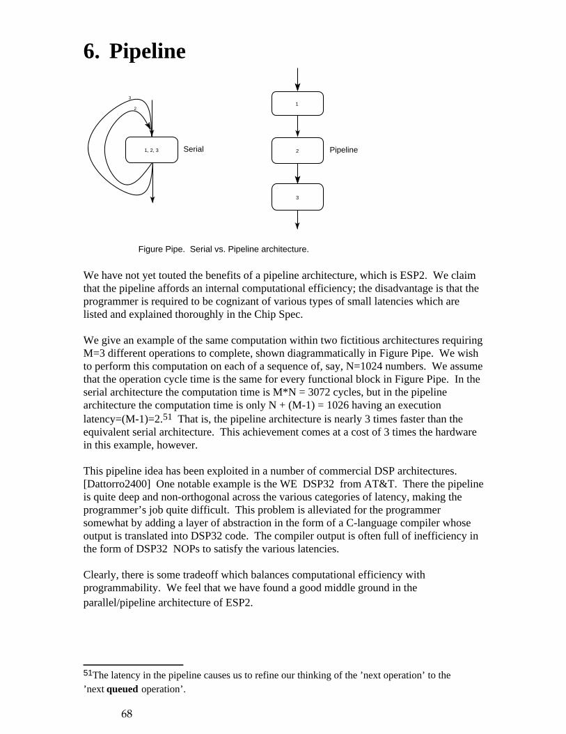
6. Pipeline
Figure Pipe. Serial vs. Pipeline architecture.
Serial Pipeline1, 2, 3
1
2
3
2
3
We have not yet touted the benefits of a pipeline architecture, which is ESP2. We claimthat the pipeline affords an internal computational efficiency; the disadvantage is that theprogrammer is required to be cognizant of various types of small latencies which arelisted and explained thoroughly in the Chip Spec.
We give an example of the same computation within two fictitious architectures requiringM=3 different operations to complete, shown diagrammatically in Figure Pipe. We wishto perform this computation on each of a sequence of, say, N=1024 numbers. We assumethat the operation cycle time is the same for every functional block in Figure Pipe. In theserial architecture the computation time is M*N = 3072 cycles, but in the pipelinearchitecture the computation time is only N + (M-1) = 1026 having an executionlatency=(M-1)=2.51 That is, the pipeline architecture is nearly 3 times faster than theequivalent serial architecture. This achievement comes at a cost of 3 times the hardwarein this example, however.
This pipeline idea has been exploited in a number of commercial DSP architectures.[Dattorro2400] One notable example is the WE DSP32 from AT&T. There the pipelineis quite deep and non-orthogonal across the various categories of latency, making theprogrammer’s job quite difficult. This problem is alleviated for the programmersomewhat by adding a layer of abstraction in the form of a C-language compiler whoseoutput is translated into DSP32 code. The compiler output is often full of inefficiency inthe form of DSP32 NOPs to satisfy the various latencies.
Clearly, there is some tradeoff which balances computational efficiency withprogrammability. We feel that we have found a good middle ground in theparallel/pipeline architecture of ESP2.
51The latency in the pipeline causes us to refine our thinking of the ’next operation’ to the ’next queued operation’.
68
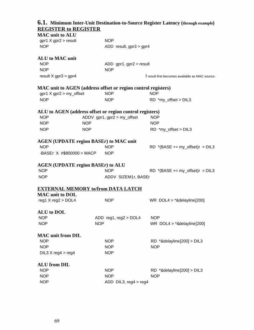
6.1. Minimum Inter-Unit Destination-to-Source Register Latency (through example)REGISTER to REGISTERMAC unit to ALU gpr1 X gpr2 > result NOP NOP ADD result, gpr3 > gpr4
ALU to MAC unit NOP ADD gpr1, gpr2 > result NOP NOP
result X gpr3 > gpr4 ! result first becomes available as MAC source.
MAC unit to AGEN (address offset or region control registers) gpr1 X gpr2 > my_offset NOP NOP
NOP NOP RD *my_offset > DIL3
ALU to AGEN (address offset or region control registers) NOP ADDV gpr1, gpr2 > my_offset NOP NOP NOP NOP
NOP NOP RD *my_offset > DIL3
AGEN (UPDATE region BASEr) to MAC unit NOP NOP RD *(BASE += my_offset)r > DIL3
-BASEr X #$800000 > MACP NOP
AGEN (UPDATE region BASEr) to ALU NOP NOP RD *(BASE += my_offset)r > DIL3
NOP ADDV SIZEM1r, BASEr
EXTERNAL MEMORY to/from DATA LATCHMAC unit to DOL reg1 X reg2 > DOL4 NOP WR DOL4 > *&delayline[200]
ALU to DOL NOP ADD reg1, reg2 > DOL4 NOP NOP NOP WR DOL4 > *&delayline[200]
MAC unit from DIL NOP NOP RD *&delayline[200] > DIL3 NOP NOP NOP DIL3 X reg4 > reg4 NOP
ALU from DIL NOP NOP RD *&delayline[200] > DIL3 NOP NOP NOP NOP ADD DIL3, reg4 > reg4
69

7. IndirectionThe chip hardware provides an indirection mechanism for accessing internal registers.Recall that the ALU employs the operands named A, B, and C, while the MAC unitemploys D, E, and F, and the AGEN unit has the G operand (which is an AOR). TheALU MOV instruction, for example, moves the source operand B to the destinationoperand C, while the MAC unit moves D to F.
NOP MOV B > CMOV D > F
As is always the case for indirection in the ALU, the INDIRA and INDIRB pointer SPRshold the register address of the A and B source operands, respectively, while the INDIRCpointer SPR holds the register address of the C destination operand. If we want toindirect on the C operand, for example, we must first place the desired destination addressinto the pointer register, INDIRC. We might accomplish this as follows:
DEFGPR gpr source=17 destDEFREGION R aorCODEMOV #gpr > INDIRC !move register address
NOP MOV source > INDIRECT
When the ALU sees the INDIRECT SPR in the C operand field, it substitutes thecontents of INDIRC for the C operand address. So in this example, the contents ofsource (=17) are moved to the GPR called gpr, because INDIRC holds the registeraddress of gpr.
We point out a potential pitfall here which arises in the coding of abbreviated instructionsemploying implied destinations. This occurs, for example, when the ALU construct,
OPERATION A, INDIRECT ! not recommended
is used in place of the verbose construct,OPERATION A, INDIRECT > INDIRECT
The first construct implies that the destination register address, inside INDIRC, is thesame as the second source register address, inside INDIRB. Since INDIRB cannot holdthe destination address of any instruction, then the first construct can only work asimplied if the programmer has preloaded both INDIRB and INDIRC with the sameaddress.
So, for indirection to work properly with no caveat, only the following constructs should be used in the
ALU:
OPERATION INDIRECT, B
OPERATION INDIRECT, B > C
OPERATION A, INDIRECT > INDIRECT
OPERATION INDIRECT, INDIRECT > INDIRECT
70

It is much easier to remember that for indirection to work as intended, use the verboseALU construct:
OPERATION A, B > C
substituting INDIRECT where desired. An exception occurs for the use of indirection inconjunction with the ALU’s ASDH, ASDL, LSDH, and LSDL double precision shiftinstructions. Consult the Chip Spec.
Of course, the INDIRINC and INDIRDEC SPRs may be substituted for any INDIRECTSPR. The use of these two SPRs as operand automatically post-increment/decrements thecorresponding pointer register.
The MAC unit has its own pointer registers corresponding to its D, E, and F operands:INDIRD, INDIRE, and INDIRF. The AGEN unit has INDIRG. In general, there is lessabbreviation allowed by the assembler in the MAC unit than in the ALU, and there is noabbreviation in the AGEN. So, the programmer is less likely to run into trouble codingindirection in the MAC unit or AGEN.52
Pseudo instructions are plentiful in both the ALU and MAC unit, so the programmer mustconsult the Chip Spec. to determine how operands get mapped for each individualpseudo. In some cases, the programmer may need to resort to the instruction primitivesto get the desired result.
To reiterate the general rule: always use verbose constructs when coding indirection.
52Recall that the E operand in the MAC unit cannot be an AOR; likewise INDIRE cannot pointto an AOR.
71

7.1. Indirection, Minimum Latencies (through example)
MAC unit to MAC unit sourceMOV #gpr > INDIRD ! same latency for INDIRENOPMOV INDIRECT > dest
MAC unit to MAC unit destinationMOV #gpr > INDIRF NOPMOV source > INDIRECT
ALU to ALU sourceNOP MOV #gpr > INDIRB ! same latency for INDIRANOPNOP MOV INDIRECT > dest
ALU to ALU destinationNOP MOV #gpr > INDIRC NOPNOP MOV source > INDIRECT
MAC unit to ALU source or destinationMOV #gpr > INDIRB ! same latency for INDIRA or INDIRCNOP MOV INDIRECT > dest
ALU to MAC unit source or destinationNOP MOV #gpr > INDIRF ! same latency for INDIRD or INDIRE NOPMOV source > INDIRECT
MAC unit to AGEN G operand (RD or WR)MOV #aor > INDIRG NOPNOP NOP RD *(INDIRECT)r > DILn
ALU to AGEN G operand (RD or WR)NOP MOV #aor > INDIRG NOPNOP NOP RD *(INDIRECT)r > DILn
72

ESP2Ensoniq Signal Processor 2
Part III
Fundamental Audio Applications53
Jon Dattorro
73

1. Linear and Allpass Interpolationfor Application to Chorus, Flanging, and Vibrato Effects
1.1. Audio Applications of InterpolationIn this section, we present the topic of delayline interpolation from the more intuitivepoint of view of the required fractional sample delay; i.e., a time domain viewpoint. Theclassical derivation, called sample rate conversion, [Schafer/Rabiner] [Vaidyanathan] ismore a frequency domain formulation. In a musical context, sample rate conversion ratioinverse (M/L in Appendix IX) corresponds to Pitch Change or Shift ratio. We synopsize theclassical results in Appendix IX where will be found a schematic translation of thefundamental algorithms we discuss to the more traditional DSP nomenclature. Thatshould serve to bridge the two viewpoints.
The technique of delayline interpolation is employed when it is desired to delay a signal bysome number of samples expressible as a whole plus some fractional part of a sample. Thisway, the delay is not restricted to sample boundaries hence avoiding signal discontinuitieswhen the delay time is swept. Delayline interpolation is indigenous to Pitch Change andPitch Shift54 algorithms which are themselves integral to numerous other effects; e.g.,Doppler, and Leslie Rotating Speaker emulation. Delay modulation forms the basis of theChorus effect and its close relative, the Flanger.55 Delay modulation alone (with no mix)yields Vibrato when the modulation is sinusoidal. Use of delay modulation typically entails anominal signal delay because the modulation spans some desired range.
The interpolation methods we seek are computationally simple and inexpensive bynecessity. The interpolation algorithm may be executed many times in one sample-synchronous audio processing program. Playing a subsidiary role, we typically cannotafford interpolation routines that consume a large percentage of the allotted execution time.
1.2. !*** Linear interpolation ***We show the kernel of the ESP2 code56 for Linear interpolation from Appendix XI. Theprinciples discussed in this section are applied therein.57
!********************* Linear interpolation ***************************MOV nominal_delay > MACP MACP + yqn X chorus_width > &VoiceL[ ] !address, integer part
frac X *&VoiceL[(+)] > MAC LSH MACRL >>1 > frac !fractional part (positive)
MAC + frac_u X *&VoiceL[ ] > vibrato DIFF frac > frac_u!****************************************************************
54Pitch Change and Pitch Shift are distinguished later on. 55These two effects come about when the output signal is made to be a linear sum (mix) of the original(dry) input and the dynamically delayed (wet) input signal. The Chorus and Flanger are distinguishedprimarily by the minimum delay in their delay range. (The minimum is less for the Flanger.)56ESP2 is the second-generation Digital Signal Processing chip for audio from Ensoniq Corp., Malvern,Pennsylvania, USA. Finished in 1995, it was designed to supersede the Motorola 56000 series.57The complete ESP2 program in Appendix XI is fully tested and in production.
74

The process called Vibrato58 is shown diagrammatically in Figure L. The local index mis defined as the current computed relative index into our delayline with respect to itsroot. The local index, m , requires computation because we want it modulated by theLFO (low frequency oscillator), yqn, oscillating as a function of time, n. The range of
m , ±CHORUS_WIDTH, is centered about the nominal tap point into the delayline,NOMINAL_DELAY.
frac_u
. . .2048
. . .0
2 X CHORUS_WIDTH
frac
delayline, VoiceL[2048]
Figure L. vibrato = frac X VoiceL[m+1] + (1 - frac) X VoiceL[m] This is the desired analytical result, not ESP2 syntax.
vibrato
vibrato
NOMINAL_DELAY
m = INT(m.frac)
frac = m.frac - m
m m+1
m.frac = NOMINAL_DELAY + yqn X CHORUS_WIDTH
frac_u = 1 - frac
Note from Figure L that because the time-varying fixed-point expression m.frac isalways a positive index into the delayline, then the coefficient, frac, is always positive.The time-varying positive coefficients, frac and frac_u, are 23-bit resolution becausechorus_width (assigned as CHORUS_WIDTH in the declarations) is scaled by the oscillator, yqn (q for quadrature), which is in q23 format.59
58In the context of audio effect design, Vibrato is most often defined to be undulating pitchchange although it can certainly be accomplished by other means.59See Scientific and Binary-Radix Notation.
75
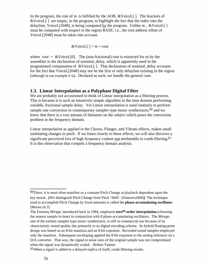
In the program, the role of m is fulfilled by the AOR, &VoiceL[ ]. The brackets of&VoiceL[ ] are empty, in the program, to highlight the fact that the index into thedelayline, VoiceL[2048], is being computed by the program. Unlike m , &VoiceL[ ]must be computed with respect to the region BASE; i.e., the root address offset ofVoiceL[2048] must be taken into account.
&VoiceL[ ] = m + root
where root = &VoiceL[0]. The (non-fractional) root is extracted for us by theassembler in the declaration of nominal_delay, which is apparently used in theprogrammed computation of &VoiceL[ ]. That declaration of nominal_delay accountsfor the fact that VoiceL[2048] may not be the first or only delayline existing in the region(although in our example it is). Declared as such, we handle the general case.
1.3. Linear Interpolation as a Polyphase Digital Filter We are probably not accustomed to think of Linear interpolation as a filtering process.This is because it is such an intuitively simple algorithm in the time domain performingvariable, fractional sample delay. Yet Linear interpolation is used routinely to performsample rate conversion in contemporary sampler-type music synthesizers,60 and weknow that there is a vast amount of literature on the subject which poses the conversionproblem in the frequency domain.
Linear interpolation as applied in the Chorus, Flanger, and Vibrato effects, makes smallundulating changes in pitch. If we listen closely to these effects, we will also discover asignificant perceived loss of high frequency content not attributable to comb filtering.61
It is this observation that compels a frequency domain analysis.
60There, it is most often manifest as a constant Pitch Change at playback dependent upon thekey struck. (We distinguish Pitch Change from Pitch ‘Shift’. [Dattorro2400]) The techniqueused to accomplish Pitch Change by fixed amounts is called the phase-accumulating oscillator.[Moore,ch.3] The Ensoniq Mirage, introduced back in 1984, employed zeroth-order interpolation (choosingthe nearest sample in time) in conjunction with 8 phase-accumulating oscillators. The Mirage,one of the earliest sampler-type music synthesizers, is still in commercial use because of itscharacteristic sound quality due primarily to its digital encoding scheme. Its hybrid floating-pointdesign was based on an 8-bit mantissa and an 8-bit exponent. Recorded sound samples employedonly the mantissa. Subsequent enveloping applied the 8-bit exponent to the analog reference on aD/A converter. That way, the signal to noise ratio of the original sample was not compromisedwhen the signal was dynamically scaled. -Robert Yannes61When a signal is added to a delayed replica of itself, comb filtering results.
76

Ζ-1
x
x
∑
Figure PL. Linear interpolation circuit.
1 - frac
frac
x[n-m] v[n]
x[n-(m +1)]
In Figure PL we show the actual two-input linear time-varying digital circuit (in DSPformat) which implements standard Linear interpolation. We have drawn it in a strangeway to emphasize the non-sequential access of the required input samples. The timeindex, n, steps through discrete time in a sequential fashion; 0 < n < ∞ . The index, n,always refers to the current sample.
In the circuit, the z-1 (unit delay) is not terminated because the local index, m , is time-varying (it changes at each time step, n), which is to say that it can take on any valuewithin bounds.62 From the declarations in our program we have implicitly establishedthe parameters: 0 < m < 2048 . The consequence of these considerations is that x[n-1-m] is not necessarily the old value of x[n-m].
Ideally what we want is for v[n] to approximate the value of the continuous signal x(t)at points in time between sample instants; i.e., we would like
v[nT] ≈ x((n - m.frac)T) (lipdf)
where T is the sample period. The Linear interpolation circuit makes this approximation(lipdf), but it is a time-varying circuit63 because its coefficients are a function of m.fracas outlined in Figure L. The circuit of Figure PL is polyphase because whenever anoutput sample v[n] is computed, a new pair of coefficients is fetched yielding a differentphase response from one of the filters in an ordinal set.64 [Vaidyanathan,pg.166] Noticethat when frac=0, which is not unusual, the circuit performs no filtering action; i.e.,allpass.
62Strictly speaking, m is a function of n; i.e., m(n). Its non-sequential nature demands randomaccess of external memory.63It is possible for a polyphase network to be time-invariant even when the constituting circuitsare time-varying. This happens when the output signal is a replica of the input signal to within aconstant and/or a delay term. [Vaidyanathan]64The number of possible coefficients is related to their resolution; there are L=223 possible pairs ofcoefficients, hence that many polyphase filters. [Crochiere/Rabiner,ch.4.3.11]
77

To make the connection from the circuit to our program, we make the analyticalidentification:
x[n-m] = VoiceL[m] !not ESP2 syntax65
This identification locates the requested sample in our delayline. It is clear that x[n]always refers to VoiceL[0] as this is the current sample. This is true because BASEV isdecremented in the program, and positive m indexes older samples in our delayline.
1.3.1. High-Frequency Loss of the Linear InterpolatorTo facilitate the investigation, we will approximate the actual circuit used (shown inFigure PL) with the polyphase filter circuit in Figure PL2. We can do this because thetwo inputs in Figure PL are separated by one sample in the delayline. We need notassume constant m for the analysis because we will view the instantaneous transferfunction of this non-recursive network,66 represented by Figure PL2.
Figure PL2. Linear interpolation analytical circuit approximation.
Ζ-1
x
x
∑1 - frac
frac
x[n-m] v’[n]
Because of the constant interrelationship of the time-varying coefficients, the circuitapproximation has an instantaneous frequency response that traverses a domain having anallpass transfer function [1, z-1) at either extreme of the coefficients, to an averaging
transfer (1 + z-1) /2 in the middle. This large set of transfers are the frequencyresponses of the polyphase filters. In Figure PLS we show several of these transfers,corresponding to different values of frac.
65Delayspecs in the form of external memory array references expect constant expressionswithin the brackets.66We freeze time and then determine the transfer function at that moment. This analyticaldevice is justifiable if m changes slowly in time. The circuit approximation in Figure PL2 isonly used for analysis; it is not used in the actual implementation.
78
0 0.1 0.2 0.3 0.4 0.5
0.2
0.4
0.6
0.8
1
ω/2π
V’(ejω)
X(ejω)
Figure PLS. Spectra of Linear interpolation polyphase filters.
[1, z-1)
(1+z-1)/2
It is this set of transfer functions in Figure PLS that we hear in our effects.67 In somecases, flutter is clearly audible and objectionable. In other cases, a veil seems to havebeen placed over the sound source.
We could eliminate this artifact if the polyphase filters were allpass. So we need to knowif it is possible to make the individual polyphase filters have allpass transfers while stillperforming interpolation. The answer is in the affirmative [Vaidyanathan,pg.166][Renfors/Saramäki] and we explore this in the section, Allpass Interpolation.68
67Each curve below the single allpass is duplicated since there are two sets of coefficients
corresponding to each curve in the case of Linear interpolation (for example, (0.25 + 0.75 z-1)
and (0.75 + 0.25 z-1)).68The reason that the polyphase filters can have allpass transfer is because:
The formal frequency domain formulation of interpolation derives the polyphase filtersfrom what is called the prototype interpolation filter. The prototype filter is simply asuccessively delayed sum of the L polyphase filters
H(z) = ∑l e-jωl El(ej ωL)
constituting the complete set. [Vaidyanathan,ch.4.3] The prototype filter response mustnot be allpass, by definition, but no such restriction is placed upon the individualpolyphase filters! In fact, for the idealized formulation of interpolation by a rationalfactor, each polyphase filter is exactly allpass; (See Appendix IX for interpretation.)
El(ejω) = ej((ω-2πm)l/L)
where l is the polyphase filter number, L is the upsampling rate, m is the prototypereplication number or the frequency-band number of an Lth-band (Nyquist(L))prototype. [ibid.,pg.168,109,124] [Crochiere/Rabiner,ch.4.2.2]
When we sum all the successively delayed non-allpass polyphase filters of Linear interpolation we
79
ω / 2π
Figure PLD. Delays of Linear interpolation polyphase filters.The extreme polyphase filter z-1 is not used.
samples
0 0.1 0.2 0.3 0.4 0.5
0.2
0.4
0.6
0.8
1z-1
(1+z-1)/2
Figure PLD shows the delay transfer as a function of frequency introduced by the polyphasefilters corresponding to Figure PLS. The fractional sample delay is figured as the negative ofthe phase response divided by the radian frequency; i.e., the phase delay. This signal delayis with reference to a steady state sinusoid of infinite duration.
The delay transfers of the polyphase filters are as important as their frequency transfers.When the coefficient, frac, calls for a quarter-sample delay, for example, we would like aconstant quarter-sample delay for all frequencies. The only delay transfer of Linear
interpolation that perfectly meets this criterion is the one in the middle, (1 + z-1) /2; i.e., it isthe only one, aside from the trivial case of frac=0, that we will see having linear phase,hence a constant delay (half-sample, this case). It is observed from Figure PLS andFigure PLD, that when the filtering is at its worst the delay is perfect.
Notice that the delay for each individual polyphase filter in Figure PLD is fairly constant inthe low frequency region, however. If we regard only DC, we make the further observationthat the delay perfectly tracks the polyphase filter coefficient, frac, as desired. This propertyis a major determinant in the performance of the Linear interpolator from the standpoint ofTHD+N of low frequency signals.
get the transform of a sampled triangular finite impulse response, which is what we expect from theprototype. [Crochiere/Rabiner] [Opp/Sch,pg.109]
80

Figure PLA. Average Delay of each Linear interpolation polyphase filter.
samples
0.2 0.4 0.6 0.8 1
0.2
0.4
0.6
0.8
1
frac = filter no. / 223 ≡ l / L
Figure PLA shows the average delay (over frequency) of each individual polyphase filterfor the Linear interpolator. There are L=223 different polyphase filters because that ishow many different non-negative coefficients there are in 24-bit two’s complement, q23format. [Crochiere/Rabiner,ch.4.3.11] The straight line is the desired average.
81

1.4. Allpass InterpolationThe implementation cost vs. performance of Linear interpolation is difficult to beat,especially as the nominal sample rate is increased. It does have significant drawbacks,however, which motivates us to look for better methods.
The drawbacks to the use of Linear interpolation are:1) it is a lowpass process having a dynamic zero at the Nyquist frequency creatingmuffled sounds and unaccounted damping in signal paths employing this process,2) the dynamic zero of its polyphase digital filters introduces audible flutter (amplitudemodulation) which is quite objectionable near unity Pitch Change Ratio for soundshaving much high frequency content,3) an exceptional amount of aliasing occurs and is worst for large pitch change upwards,corresponding to the case of sample rate reduction (decimation).69
Other companies [Rossum] report alternative interpolation strategies.70 The authorrecommends Lagrange interpolation [Crochiere/Rabiner] [Schafer/Rabiner] [Ramstad][Laakso/Välimäki] which is an analytical extension to Linear interpolation.71 But non-recursive FIR (finite impulse response) techniques such as these have a high computational cost.Nonetheless, FIR filters dominate contemporary sample rate conversion practice because fromthe point of view of internal truncation noise, it is difficult to mess up an FIR implementation.[Dattorro89] [DattorroPat.] [Andreas] Also, FIR filters offer linear phase.72
69This last problem comes about because the prototype Linear interpolation filter has (one-sided)bandwidth π/L in the Vaidyanathan sense; the same is true for Allpass interpolation. The bandwidth isnot a design parameter, but falls out as a result of the implementation. When the decimation rate Mexceeds the interpolation rate L, aliasing is traditionally tolerated for these two techniques. When ourmusical applications of interpolation operate only over a microtonal conversion ratio, then aliasing is lessof an issue.70The E-mu Proteus sampling music synthesizer (1989) and its relatives all employ 7th-orderinterpolation polynomials. They aren’t exactly ‘Lagrange’ though. They use a technique in which aRemez Exchange is applied to an ‘ideal’ filter response similar to that of Lagrange, but having lowermaxima in the stopband. This gives the deep notches advantageous in the Lagrange approach, but alsothe superior stopband rejection of a sinc-based design. For more information, see the US patent on thefundamental E-mu G-chip interpolator; No.5,111,727. -David Rossum71i.e., a higher-order polynomial curve fit using more signal values, and which is maximally flat in thefrequency domain while suppressing ripple in the time domain. The two-point Lagrange interpolator isequivalent to Linear interpolation.72Generally speaking, a linear phase prototype interpolation filter does not guarantee linear phasepolyphase filters, and vice versa. Linear interpolation, for example, is a classical case of an FIR prototypethat is linear phase (having a symmetrical triangular impulse response of length 2L spanning two original samples
by design [Opp/Sch,pg.109] [Crochiere/Rabiner]) but whose polyphase filters are not. But if a linear phaseprototype is perfectly bandlimited to π/L, for L a rate conversion factor, then all its L polyphase filters
will also be linear phase; ideally of the form El(ejω) = ej((ω-2πm)l/L) where m is the frequency-band
number of an Lth-band (Nyquist(L)) prototype. [Adams,pg.545] [Vaidyanathan,pg.168] [Opp/Sch,ch.5.7](See Appendix IX for interpretation.) Crochiere [Crochiere/Rabiner,ch.4.3.6-4.3.10] gives explicit generaldesign procedures for simultaneously linear phase FIR polyphase and prototype interpolation filters.
82
Recursive polyphase filters have not been popular because they are not linear phase, ingeneral.73 The practice of recursive digital filtering requires an understanding of fixed-point arithmetic, truncation noise recirculation, [Dattorro] and transient phenomena.
We present here the simple recursive technique of Allpass interpolation which is usefulprimarily for microtonal changes in pitch (less than ±one semitone). Linear interpolationwill outperform it from the standpoint of the Total Harmonic Distortion plus Noise74
(THD+N). Otherwise, Allpass interpolation eliminates the drawbacks of Linearinterpolation in this microtonal region, and makes the interpolation sound analog.
Figure PA. Allpass interpolation circuit. JonD 1994
Ζ-1
x ∑1 - frac
x[n-m] a[n]
Ζ-1
x1 - frac
x[n-(m +1)]
Figure PA, a modification to Figure PL, shows the actual circuit used to implement Allpassinterpolation. [Smith/Friedlander] Our application of Figure PA employs time-varying filtercoefficients. The formal derivation of the ideal network [Vaidyanathan] [Renfors/Saramäki]requires as many recursive memory elements as there are coefficients (L=223 in 24-bit (q23 format)two’s complement).75 In the ideal network, the filter coefficients are fixed. That is one reasonwhy this simpler network in Figure PA (employing only one recursive element with a time-varying
coefficient) only performs well (in terms of THD+N) for small pitch changes. Making the sameanalytical circuit approximation as before, we can see that connection of the node at x[n-(m +1)]instead to the unit delay would make the instantaneous transfer function of the resulting polyphasefilter, allpass. This means that the polyphase interpolation circuit in Figure PA has a frequencyresponse which is approximately allpass; |A(ejω)/X(ejω)| ≈ 1.
73Renfors’ IIR design offers nearly linear-phase recursive polyphase and prototype interpolationfilters. [Renfors/Saramäki]74This is a measure of signal purity which aggregates everything that is not signal, and thenrelates that to some purified reference which is usually the signal itself. THD+N distortion isinherent to either interpolation process.75Each recursive memory element resides in a structure like Figure PA having the feedforward delayelement connected. See Appendix IX. Our simulations have shown that as few as L=28 recursiveelements work quite well to make constant or sweeping Pitch Change over a large range. For theanalogous case in Linear interpolation, also see [Crochiere/Rabiner,pg.81,ch.4.3.11] which shows thatLinear interpolation is ideally implemented because of the lack of any long term memory.
83

As shown in Figure PA, the time-varying coefficients (frac_u=1-frac) are easily derived fromm.frac as in Figure L. We find that, subjectively, the circuit of Figure PA sounds quitesmooth in musical applications. But, analytically speaking, the desired signal-delay introducedby the circuit approximation does not track frac as well as it does for Linear interpolation.
ω / 2π
Figure PAD. Delays of Allpass interpolation polyphase filters.The extreme polyphase filter z-1 is not used.
ample
0 0.1 0.2 0.3 0.4 0.5
0.2
0.4
0.6
0.8
1z-1
(1+0.95z-1)
(0.95+z-1)
Figure PAD is the plot corresponding to Figure PLD. Notice how the delay between filters isspaced unevenly; especially noticeable at DC. But for each individual filter, the delay is stillfairly constant in the low frequency region.
Figure PAA. Average delay of each Allpass interpolation polyphase filter.
ample
0.2 0.4 0.6 0.8 1
0.2
0.4
0.6
0.8
1
frac filter no / 223 ≡ l / L
84

Surprisingly, the average delay (over frequency) of each polyphase filter, shown inFigure PAA, is better than that for Linear interpolation (compare to Figure PLA).
It is reasonable to expect that we could force the delay of each polyphase filter to beequal to any desired value at a particular frequency by appropriately altering thepolyphase filter coefficients. This would be beneficial were we concerned with THD+Nperformance in a particular frequency region.
Indeed, the exact equation to warp the allpass circuit coefficients in Figure PA is[SmithIII,pg.178]:
sin( ω (1 τ ) )2
sin( ω (1 + τ ) )2
1 - frac
where τ is the desired fractional sample delay at ω, the desired normalized radianfrequency. We can eliminate the dependency of the equation upon signal frequency ωwhen we are primarily concerned with THD+N performance at low frequencies(ω near 0). For then the coefficient warp equation simplifies to:
≈ (1 - τ )
(1 + τ )1 - frac = 1/3 + ∑
i =1
∞ (-2)i+2
3i+1(τ - 1/2)i (sw.eq)
This is a reasonable substitution for audio signals. From Figure L we can see that thedesired fractional sample delay is frac, so we make the identification, τ = frac .
Figure WPA. Warped Allpass interpolation circuit. JonD 1994
Ζ-1
x ∑x[n-m] aw[n]
Ζ-1
xx[n-(m +1)]
1 - frac1 + frac
1 - frac1 + frac
Figure WPA shows the actual time-varying circuit used to implement warped Allpassinterpolation using the simplified warp equation (sw.eq) in place of the allpasscoefficients shown in Figure PA.
85

0 0.1 0.2 0.3 0.4 0.5
0.2
0.4
0.6
0.8
1
ω / 2π
Figure PADW. Delays of Allpass interpolation warped polyphase filters.The extreme polyphase filter z-1 is not used.
samples
(1 + 0.95/1.05 z-1)
(0.95/1.05 + z-1)
z-1
Figure PADW demonstrates the even distribution of delay across the polyphase filters atlow frequency using the simplified warp equation (sw.eq) as shown in Figure WPA. Thiscloser tracking between frac and signal delay will help improve somewhat the THD+Nperformance at low frequencies.
Figure PAAW. Average delay of each Allpass interpolation warped polyphase filter.
samples
0.2 0.4 0.6 0.8 1
0.2
0.4
0.6
0.8
1
frac = filter no. / 223 ≡ l / L
86

But the improvement to delay distribution in the low frequency range causes the averagedelay shown in Figure PAAW to suffer as we might expect (compare to Figure PAA).We find, analytically, that for Allpass interpolation of low frequency sinusoids on up to afew kHz, use of the simplified coefficient warp equation (sw.eq) is desirable from aTHD+N standpoint. But for some of our musical applications we have not found itabsolutely necessary to implement the circuit using different coefficients than thoseshown in Figure PA. Within an ESP2 implementation, however, several computed termsfrom the Taylor series expansion (sw.eq) of the simplified warp equation (or a table lookup
routine) would easily map 1-frac to the warped coefficients of Figure WPA. Wedemonstrate this shortly.
Distortion Analysis
0.96 0.98 1 1.02 1.04 1.06
-100
-80
-60
-40
-20
0.96 0.98 1 1.02 1.04 1.06
-100
-80
-60
-40
-20
(a)
(b)
dB
dB
Figure THD. Simulated THD+N of pitch-changed sinusoid due to:(a) Linear interpolation,(b) Allpass interpolation.
Pitch Change Ratio
Pitch Change Ratio
87

Figure THD estimates the Total Harmonic Distortion plus Noise of a 16-bit 401 Hz sinusoid,sampled at 44.1 kHz, for various constant pitch changes spanning ±one semitone. The C-program simulation which produced the THD+N estimates in Figure THD (b), employs thesimplified warp equation (sw.eq) and 16-bit polyphase filter coefficients. Without (sw.eq), theTHD+N in (b) would be about -44 dB. The polyphase filter coefficients used to makeFigure THD (a) are 8-bits in width.
The employment of Allpass interpolation now warrants consideration of transient phenomena aswell as truncation error recirculation: The predominant artifact exposed in Figure THD (a)(Linear interpolation) is harmonic distortion due to the facts: 1) the two-tap FIR magnitude transferis modulated by the time-varying coefficients, and 2) the actual delay of the two-tap FIR deviatesfrom the desired time-varying delay. The predominant artifact exposed in Figure THD (b)(Allpass interpolation), however, is distortion due to transients arising from the time-varyingpolyphase filter coefficients. Even though the filter coefficients are updated at the sample rate,the nature of the Pitch Change/Shift algorithm (as outlined in Figure L) demands a disjunct sequenceof desired fractional-sample delay. While truncation noise is a second-order artifact in bothcases, we mention that truncation post-accumulation, as can be seen in the ESP2 programs, isemulated.
1.5. ESP2 Programs for Allpass InterpolationWe show the required changes to the ESP2 Linear interpolation program to implementAllpass interpolation by two of the methods discussed above. The following sections of codewould each replace the corresponding section labelled !*** Linear interpolation *** . Thisfirst implementation does not employ coefficient warping.
!***************** Allpass interpolation ******************JonD 12/30/94***********NOP MOV #2.**-8. q24 > MACP_L !1/256th sample offset
MOV nominal_delay > MACP_H MOV *&VoiceL[(+)] > MACP !to second seed
MACP + yqn X chorus_width > &VoiceL[ ]
MACP + frac_u X *&VoiceL[ ] > MAC LSH MACRL >>1 > frac ! q23
MAC - frac_u X vibrato > vibrato DIFF frac > frac_u!************************************************************************
The code above implements the digital circuit in Figure PA having time-varying coefficientsderived as in Figure L. The total cost of this Allpass interpolator is one more line of ESP2code over that for the Linear interpolator.
We require the implementation to prevent prolonged Nyquist (Fs / 2) oscillation that comesabout when frac=0. This happens whenever chorus_width is set to zero by the system host.We minimize Nyquist oscillation by forcing the circuit to interpolate by a constant fraction ofa sample at all times. (That is the purpose of the first line of code above.) This techniqueintroduces a constant fractional offset into the equation for m.frac in Figure L (not shownthere), and has little deleterious audible consequence.
Next we consider coefficient warping to improve the processing THD+N:
88
DEFGPR Taylor nest!***************** warped Allpass interpolation ************ JonD 5/22/95************
MOV nominal_delay > MACP MOV *&VoiceL[(+)] > MACPMACP + yqn X chorus_width > &VoiceL[ ]
MACP + frac_u X *&VoiceL[ ] > MAC LSH MACRL >>1 > frac MAC - frac_u X vibrato > vibrato SUB HALF, frac > Taylor
MOV #-32./81. > MACP MOV #16./27. > MACPMACP + #64./243. X Taylor > nest ASH #-8./9. >>1 > MACPMACP + nest X Taylor >>1 > nest ASH #1./3. >>1 > MACPMACP + nest X Taylor > nestMACP + nest X Taylor <<1 > frac_u !***************************************************************************
This Allpass interpolator code employs the first five terms of the Taylor series expansionof (sw.eq) to map frac into (1-frac)/(1+frac). It implements Figure WPA via the map:
frac_u = 1/3 + (frac-1/2)[-8/9 + (frac-1/2)[16/27 + (frac-1/2)[-32/81 + (frac-1/2)[64/243]]]]
Since the map is only approximate, it is no longer necessary to prevent Nyquistoscillations as before. We measure an improvement of 26 dB in THD+N over that ofthe previous Allpass interpolator code,76 attributable to the coefficient warp. Linearinterpolation exceeds this particular THD+N performance, but only by a few dB; viz.,
Measured Linear interpolation: -78 -> -88 dB Measured warped Allpass interpolation: -77 -> -85 dB
These THD+N measurements are time-varying because the sinusoid frequency is slowlymodulated by the LFO, yqn, in the code. That is why they are indicated as a range. All
polyphase filter coefficients are 24 bits, the sample rate is 44.1 kHz. As is apparent fromthe ESP2 program, truncation is post-accumulation.
Having reached parity between the two processes in terms of THD+N, we wouldpreferentially choose Allpass interpolation because it eliminates the drawbacks stated atthe outset when employed in a microtonal region.
1.6. Theoretical Extensions[Laakso/Välimäki] broadens the scope of this Allpass approach to interpolation. They provideformulae for allpass polyphase filters of higher order that possess a more linear delay vs.frequency, thereby providing a prototype interpolation filter (see Appendix IX) having higherstopband rejection. The delay linearization as follows filter order is not quite as fast as we mightlike, however. [Välimäki/Laakso] deals with transient phenomena.
76having declared the LFO Freq=0.1 Hz in a real-time ESP2 hardware development system,frequency modulating a 24-bit, 400 Hz sinusoid into an Audio Precision, Inc., analog signalanalyzer.
89

2. The White Chorus EffectAny complete discussion of the Chorus effect must consider its relative, the Flanger. Theintended goal of Chorusing is to emulate the independence of multiple like-voicesplaying in unison. But the goal of Flanging is to jolt the ear’s time-correlationmechanism by offering a signal replica delayed by an amount that is within theintegration time constant of the hearing system.77 We must first note that there is a verystrong bond between the implementation of the Chorus effect and of the sonically radicalFlange effect. What has gestated into the industry standard for this species condensessimply to a sum of the original input signal with a delayed replica. In either effect, thereplica delay is modulating and never static. The consequence of summing the twosignals is to introduce moving troughs into the input signal spectrum. In the case ofFlanging, that is the desired result; the deeper and more selective the troughs are, thebetter.78 In the case of Chorusing, the troughs are undesirable and an effort is made tolimit their depth by summing unequal amounts of original signal and delayed replica. Butthe primary distinguishing design feature of the Choruser is that the minimum of themodulated delay time is much greater than that of the Flanger. The principal reason is soas to avoid flanging, by the Choruser, which becomes subjectively more pronounced forsmall delays. Indeed, the best Flangers can sweep the delay all the way to absolute zero;no delay.
In Figure Chorus we present a modification to the industry standard two-voice Choruseffect, that attempts to compensate for the spectral aberration caused by the many troughsin the feedforward sum. The modification is the introduction of a feedback path into thedelayline, whose tap point is separate from that of the feedforward path but fixed at thecenter of the modulating delay in the feedforward path. Hence, the Chorus circuitapproximates an allpass filter when the changing delay in the feedforward path isproximal with the fixed delay in the feedback path. We prefer not to feed back amodulating signal because the modulation induces pitch change. Feeding back a pitchchanged signal produces more pitch change and becomes objectionable quickly for eitherintended effect. Feedback is gainfully employed in the Flanger in an inverse sense tomake a comb filter that increases the perceived depth of the troughs; i.e., the samecircuit can be used for both effects.
77The familiar thunder of a jet aircraft often reaches our ears by combination in air of the directand reflected engine backwash. As the aircraft changes position, the reflection time changes andDoppler due to the aircraft’s recession is introduced into both paths. The roar is more interestingas the reflection time is swept; that introduces more Doppler pitch change into the reflected path.78The Flange effect gets its name from a studio technique that sums two synchronous magnetic-tape recorder signals playing identical material. The recording engineer places the thumb on onetape flange to bring the two recorders slightly out of synchronization thus creating the effect. Inthe 70’s the Flange effect was emulated by analog phase shifting networks consisting of a cascadeof allpass filters having time-varying elements. Implemented in this manner, the problem ofdelaying a signal by brute force was overcome. These devices were called Phasers and remainpopular because the spectral troughs are not spaced harmonically, in general. While second-orderallpass filter sections of the cascade offer more control [J.O.Smith] over trough frequency andselectivity, the Phaser is well emulated in DSP using only first-order sections [Hartmann] [Beigel](which may be quieter in terms of truncation noise performance). The spectral troughs areharmonically stretched in the first-order case. In any case, global feedback enhances the effect,affecting perceived trough depth.
90
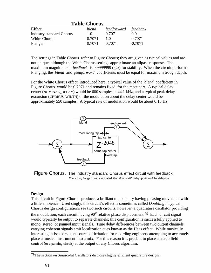
Table ChorusEffect blend feedforward feedbackindustry standard Chorus 1.0 0.7071 0.0White Chorus 0.7071 1.0 0.7071Flanger 0.7071 0.7071 -0.7071
The settings in Table Chorus refer to Figure Chorus; they are given as typical values and arenot unique, although the White Chorus settings approximate an allpass response. Themaximum magnitude of feedback is 0.9999999 (q23) for stability. When the circuit performsFlanging, the blend and feedforward coefficients must be equal for maximum trough depth.
For the White Chorus effect, introduced here, a typical value of the blend coefficient inFigure Chorus would be 0.7071 and remains fixed, for the most part. A typical delaycenter (NOMINAL_DELAY) would be 600 samples at 44.1 kHz, and a typical peak delayexcursion (CHORUS_WIDTH) of the modulation about the delay center would beapproximately 550 samples. A typical rate of modulation would be about 0.15 Hz.
fixed tapsame tap center
tap center
x
-.
blend
feedback
feedforward
modulating tap
Ζ-2048
x
x
Figure Chorus. The industry standard Chorus effect circuit with feedback.The strong flange zone is indicated; the leftmost (0+ delay) portion of the delayline.
∑∑
DesignThis circuit in Figure Chorus produces a brilliant tone quality having pleasing movement witha little ambience. Used singly, this circuit’s effect is sometimes called Doubling. TypicalChorus design configurations see two such circuits, however, a quadrature oscillator providing
the modulation; each circuit having 90o relative phase displacement.79 Each circuit signalwould typically be output to separate channels; this configuration is successfully applied tomono, stereo, or panned input signals. Time delay differences between two output channelscarrying coherent signals emit localization cues known as the Haas effect. While musicallyinteresting, it is a persistent source of irritation for recording engineers attempting to accuratelyplace a musical instrument into a mix. For this reason it is prudent to place a stereo fieldcontrol (or a panning circuit) at the output of any Chorus algorithm.
79The section on Sinusoidal Oscillators discloses highly efficient quadrature designs.
91

Flanger design would normally incorporate modulation of the same phase in each channel. Thestrong flange zone occupies approximately the first 1 ms of the delayline. The viable regionsof delay excursion for the Chorus and Flanger effects overlap, however, and can easily bedetermined by ear.
It is important to keep the Chorus circuit free of nonlinearity for those many professionalguitarists who want this effect as clean and simple as possible. For those particularguitarists, simplicity of the Chorus design is a virtue as they use this effect most all of thetime. Allpass interpolation80 for delay modulation becomes critical to the transparencyof any Chorus design. Recall that Linear interpolation is a time-varying lowpass filteringoperation. Indeed, a multi-voice Chorus design employing Linear interpolation subjectsthe signal to significantly audible amounts of low-pass filtering. We term the ChorusWhite when both negative feedback and Allpass interpolation are employed to minimizethe spectral aberration that would be consequent in the absence of these two signalprocessing techniques.
Flangers, on the other hand, can benefit from a mild nonlinearity introduced into thesignal path in front of the effect, so that the induced troughs see a more rich signal source.But Allpass interpolation is also critical to successful Flanger design so that thedynamically delayed signal remains unfiltered. Lowpass filtering of the delayed signalvia Linear interpolation would reduce the depth of the high frequency troughs; that isundesirable for a good Flanger.
CaveatFor particular types of input material (e.g., percussive signals) and subjectively longnominal delays (10 ms), the feedback path can introduce echoes which areobjectionable.81 The level of objection is somehow related to the particular form ofinterpolation. The use of the Allpass interpolator with coefficient warping (sw.eq) seemsto mitigate the echoes’ aural impact.82 In any event, one can always turn down thefeedback knob in this circumstance.
80as discussed in the Application of the same name,81The old bathroom reverberator.82We apologize for being unable to characterize this problem more accurately at this time.
92

VibratoOne might be interested to know the amount of pitch change when the blend andfeedback coefficients are 0; i.e., when the circuit is made to produce Vibrato.83 Withoutloss of generality we may consider the Vibrato applied to a sinusoid of arbitraryamplitude, A, and radian frequency, ω. Using terminology established for theInterpolation Applications, from (lipdf) we write,
x((n - m.frac)T) = A sin( ω (n - m.frac) T )= A sin( ω (n - (NOMINAL_DELAY + yqn CHORUS_WIDTH)) T )
where, yqn = sin(ωε n T), is the LFO and ωε is the radian rate of modulation
(2π Freq; see the interpolation program called Linear). NOMINAL_DELAY andCHORUS_WIDTH are expressed in units of samples.
The instantaneous radian frequency is:
Ω = ∂( ω (n - (NOMINAL_DELAY + yqn CHORUS_WIDTH)) T ) / (T ∂n)
= ω (1 - CHORUS_WIDTH ωε T cos(ωε n T))
Note that if the LFO were triangular, then the instantaneous frequency would bepiecewise constant which is unnatural, hence not desirable.
Pitch Change Ratio = Ω / ω= 1 - CHORUS_WIDTH ωε T cos(ωε n T)
This tells us that the pitch change is time-varying and proportional to the modulationfrequency and the sample period, T.
Pitch Change Ratio extrema = 1 ± CHORUS_WIDTH ωε T
83Note that this implementation of Vibrato maintains the signal’s macro-temporal features.
93

Detune EffectThere is yet another related effect which is outside the scope of the present discussion.Yet, its sonic impact is so powerful that it deserves mention; that is the Detune effect. Itis accomplished in DSP employing the class of algorithm known as the Pitch Shifter.[Dattorro2400] The Detune algorithm class employs a splicing mechanism84 (when
implemented in the time domain; see Appendix IX) to maintain the macro-temporal signalfeatures while shifting the pitch by a fixed microtonal amount using some form ofinterpolation. The pitch shifted signal is then mixed with the original. The result is oftendescribed by musicians as subjectively ‘fattening’ the sound.
This Detune effect occurs naturally and is built-in to instruments such as the pianoforte,mandolin, and twelve-string guitar. It accounts for one salient character of eachinstrument’s sound. The Chorus and Detune effects are sonically quite different, thelatter algorithm being more difficult to implement properly. The primary distinguishingfeature of the two is that the pitch is necessarily modulating in the Chorus effect becauseof the means of implementation.
The reader should also be aware that contemporary sampling music synthesizers85 oftenemulate Detuning through the use of Pitch Change, which in many cases is undesirable.
84unlike Pitch Change algorithms which have been the focus of our look into interpolation, andwhich are actually the topic of [Rossum] despite its title. The temporal features of the originalsignal are maintained in a pitch shifted replica; that is what distinguishes Pitch Shifting fromPitch Changing by fixed amounts. While many Pitch Shift algorithms employ delaylineinterpolation, the Lexicon Model 2400 Stereo Audio Time Compressor/Expander (designed bythe author in 1986 and still in production [Dattorro2400]) sidestepped the need for interpolationby incorporating a variable-rate A/D conversion system. In that design, the D/A circuitry is fixedrate, the whole instrument operating in real time on pre-recorded material.85rather sampler-type, which we distinguish from wavetable-type synthesizers,
94

3. The Low-Frequency Sinusoidal OscillatorThe low frequency sinusoidal oscillator (LFO) is ubiquitous in effect design. There areseveral implementation options: 1) direct form,2) coupled form,3) first modified coupled form,4) second modified coupled form,5) normalized waveguide.
The direct form oscillator is the most efficient option requiring only one multiply, but itis noisy unless truncation error feedback is used. [Haija/Ibrahim] [Dattorro] The errorfeedback can be implemented using only one or two adds, so it is attractive. The singlecoefficient γ requires high resolution for very low frequencies of oscillation, however.
cos( ω )
Ζ-1
Ζ-1
y1[n]
y2[n]
y1[n+1]
∑
Figure DF1. Direct Form Sinusoidal Oscillator.
y1[n] =1
y1[0] sin( n ω ) - y2[0] )(
y2[n] =1
y1[0] sin( n ω ) + y2[0] )(
sin( ω )
sin( ω )
γ = -2
x
-
y1[n+1] = -γ y1[n] - y2[n]
y2[n+1] = y1[n]
sin( ω + n ω )
sin( ω - n ω )
γ
; 0 < ω < π
-
2poles = -γ +/− j √1 − γ2
4
95
The direct form oscillator was analyzed using State-Variable theory,86 the results ofwhich are shown in Figure DF1. This type of analysis excels at finding the zero inputresponse (the ZIR). (See Appendix X.) The selected output is expressed in terms of theinitial conditions of all the memory elements, the state variables. This method of analysisdiffers considerably from the technique of solving the recursive difference equation forthe selected output, in so far as the initial conditions required by the latter are of theoutput itself. In the case of the direct form, these two methods coincide.
Obviously, by choosing the initial states y1[0] = 0 and y2[0] = -sin(ω), we get
y1[n] = sin(n ω)
There is no quadrature sinusoid at any node. But by choosing, for example, y1[0] = 1,
and y2[0] = cos(ω), we get
y1[n] = (1/sin(ω)) (sin(ω + n ω) - cos(ω) sin (n ω)) = cos(n ω)
The direct form oscillator is hyperstable87 under coefficient quantization as proven bythe equation for the pole locations in the z-plane in Figure DF1. Regardless of thequantization of γ, the pole radii are exactly 1 as determined from the pole magnitude.Any instability in the sinusoidal waveform can only be attributed to signal quantizationeffects, primarily in the form of truncation error in this recursive topology.
One must be cognizant of the relationship between oscillation frequency and amplitudewhen using the different oscillators presented in this section. The equations ofFigure DF1 predict that when frequency is changed via γ after the oscillator has beenrunning for some time, amplitude will deviate, in general. One theoretically overcomesthis problem by simultaneously updating the memory elements (the states), but this canbe difficult in practice depending upon the particular oscillator topology.
The direct form oscillator circuit can be derived from one trigonometric identity;88 viz.,
sin((n+1)ω) = cos(ω) sin(n ω) + sin(ω) cos(n ω)sin((n-1)ω) = cos(ω) sin(n ω) - sin(ω) cos(n ω)
where ω is the normalized radian frequency of oscillation (2πf T) controlled by γwhich must be in q22 binary-radix format for ESP2. Summing the two equations yields:
sin((n+1)ω) = 2 cos(ω) sin(n ω) - sin((n-1)ω)
86following the analysis presented in [Gordon/Smith] for the coupled form and the secondmodified coupled form,87We shall define ’hyperstable’ in this context to mean stability of oscillation in the face ofcoefficient quantization. The effect of signal quantization in networks is not included in thisdefinition.88This was pointed out to the author by Michael Chen.
96

Making the substitution, y1[n] <- sin(n ω) , we get
y1[n+1] = 2 cos(ω) y1[n] - y1[n-1]
which is the difference equation for the circuit.89
The coupled form is an established topology known by several names including theRader/Gold, and normal form. The coupled form is a state-space digital filter structureand is one of the foremost contributions of the branch of Linear System theory known asState-Variable analysis. The coupled form has many attributes including low truncationnoise and low coefficient sensitivity, respectively due to signal and coefficientquantization within a finite precision machine. [Jackson,ch.4.4] The latter attributemakes tuning easier. Its primary detriment is that four multiplys are required in itsunmodified form.
The unmodified coupled form in Figure X (a) shows the four multiplys required foroscillation, including two cos(ω) coefficients. Using all four coefficients, the polelocations are ideally on the unit circle. It can be deduced from the equations given inFigure X (a) that for any initial states (y[0], yq[0]) the outputs at y[n] and yq[n] yield
quadrature sinusoids. But when the ideal filter coefficients become quantized to theirrepresentation in a finite precision machine, the pole locations are perturbed in a directiondependent upon the polarity of the coefficient quantization error.90 The impact of this isthat the pole radii are no longer exactly 1, so the oscillator amplitude either decays to zeroor clips (assuming automatic saturation arithmetic) after some time has past. We do notrelish the four multiply requirement and we recall that the direct form does not sufferfrom this particular problem. This is because the direct form pole radii can be fixed bythe second-order recursive coefficient [Dattorro,(30)] which is always precisely set to 1for our present application.
The coupled form has a simpler trigonometric derivation, but uses two identities; viz.,
cos((n+1)ω) = cos(ω) cos(n ω) - sin(ω) sin(n ω)
sin((n+1)ω) = sin(ω) cos(n ω) + cos(ω) sin(n ω)
Making the substitutions, y[n] <- sin(n ω), yq[n] <- cos(n ω), we get
yq[n+1] = cos(ω) yq[n] - sin(ω) y[n]
y[n+1] = sin(ω) yq[n] + cos(ω) y[n]
89This also happens to be the generating recurrence relation of the Chebyshev polynomials;Tn+1(x) - 2x Tn(x) + Tn-1(x) = 0. [Hamming,pg.473]90The availability of the ROUND(), INT(), or BTRUNC() in-line assembler truncation functionsnow warrants appreciation.
97

cos(ω))n1
ε = ; ω < π/2
cos(ω)
Ζ-1
Ζ-1
yq[n]
y[n]
yq[n+1]
y[n+1]
∑
∑
xεεx
-
Figure X. (a) Coupled Form (Four Multiplier) Sinusoidal Oscillator.
(b) First Modified Coupled Form (Two Multiplier) Low Frequency Oscillator.
x
x
yq[n+1] = yq[n] - ε y[n]
y[n+1] = ε yq[n] + y[n]
sin(ω)
cos(ω)
yq[0] sin(n ω) + y[0] )(
cos(n ω)(
yq[n+1] = yq[n] - ε y[n]
y[n+1] = ε yq[n] + y[n]
yq[n] = yq[0] cos(n ω)
sin(n ω) - y[0]
y[n] = yq[0] sin(n ω) + y[0]
cos(n ω)
ε = sin(ω) ; ω < π
(a)
(b)
yq[n] = yq[0] cos(n ω)
sin(n ω) - y[0] )(
poles = 1 +/- j ε
poles = +/- j ε
cos(ω)cos(ω)
cos(ω)
y[n] =
)n
( 1
cos(ω) 1~~
cos(ω) 1~~
98

We will make a modified coupled form digital filter behave as an oscillator by placing itspoles either slightly beyond or precisely on the unit circle in the z-plane, even in thepresence of coefficient quantization error. We will see that both of these choices of polelocations can be achieved using only two multiplys, and both have useful purposes.
If the coupled form oscillator is employed as an LFO, we make the observation that thetwo cos(ω) coefficients are close to 1. If we set them to 1 permanently, we eliminatetwo multiplys and arrive at the first modified coupled form in Figure X (b). Using thefirst modified coupled form, the quadrature sinusoids at y[n] and yq[n] will always clip
somewhat (assuming saturation arithmetic) because the pole radii are in excess of unity.When the oscillator frequency is very low, the clipping will be slight.
The advantage of this first modified coupled form implementation is that its outputamplitude is at least unity, even after frequency is abruptly changed. The oscillator neverblows up, as the equations in Figure X (b) would predict, because of the saturationnonlinearity built into the ESP2 computation units. The detriment to the use of thisoscillator is that the tuning frequency is practically restricted to a portion of the firstquadrant in the z-plane.91 This modified coupled form of the oscillator would be chosenwhen the criteria for selection of an LFO does not include sinusoid purity, but fullamplitude stable quadrature signals are a must.
The second modified coupled form, first presented in [Gordon/Smith], is shown inFigure X+1. This oscillator produces a high purity sinusoid at the two outputs, y[n] andyq[n], whose noise floor is low enough to characterize D/A converters. The two outputs
are no longer exactly in quadrature as before,92 but the oscillator is hyperstable becausethe pole radii are exactly 1 even when epsilon is quantized.93 The tradeoff for thisstability is the linking of amplitude to frequency of oscillation as seen in the equations inFigure X+1. By observation of the poles, the tuning frequency now spans DC to Nyquistas epsilon goes from 0 to 2, and so the range of oscillation is not restricted to lowfrequencies as in the first modified coupled form.
We have found as predicted, using the second modified coupled form, that when epsilon(the frequency control) is abruptly changed, the oscillator amplitude will change itself toa new value. This is because we ignore the new initial states, yq[0] and y[0], at the
time of the frequency change; i.e., no attempt is made to adjust them. We observed theseconsequent deviations in amplitude and empirically found them to be less than a decibelover a very useful range of frequency for an LFO. It was never found necessary, in anyof our applications, to compensate for these small changes in amplitude. The built-insaturation arithmetic within the ESP2 computation units eliminates any possibility oflong-term clipping, completely.
91This restriction is overcome in practice by running the oscillator twice as fast, which meanstwice the code.92From the equations in Figure X+1, it can be shown trigonometrically for any initial states thatthe two sinusoids are in a near quadrature relationship; being off by exactly 1/2 sample at anyfrequency of oscillation. This was first pointed out to the author by Timothy S. Stilson.93Like the direct form, any instability in the sinusoidal waveform can only be attributed to signalquantization effects, primarily in the form of truncation error in this recursive topology.
99
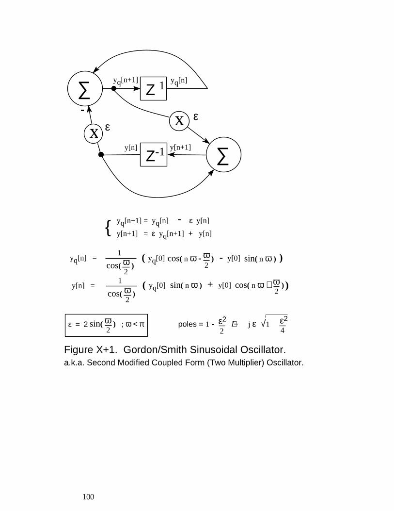
cos( ω )cos( n ω + ω )
cos( n ω - ω )
2
yq[n+1] = yq[n] - ε y[n]
y[n+1] = ε yq[n+1] + y[n]
Ζ 1
Ζ-1
yq[n]
y[n]
yq[n+1]
y[n+1]
∑
∑
x εεx
-
Figure X+1. Gordon/Smith Sinusoidal Oscillator.a.k.a. Second Modified Coupled Form (Two Multiplier) Oscillator.
2yq[n] =
1 yq[0]
sin( n ω ) - y[0] )(
y[n] =1
yq[0] sin( n ω ) + y[0] )(
cos( ω )2
2
ε = 2 sin( ω ) ; ω < π
2 2poles = 1 - ε2
+/− j ε4
√1 ε2
100

The ideal digital integrators, 1/(1 - z-1), have never presented a problem in practicebecause there is a zero of transmission at z=1 (DC) across each embedded integratorfrom its input to its output. This comment applies to both modified coupled forms.
The second modified coupled form oscillator ESP2 code, shown within the LinearInterpolation Application, is written such that if several oscillator routines were cascaded,the interleaved code resulting would be most efficient in terms of program space. Thecascaded routines would then average about two program lines per oscillator. That codefor one oscillator is reproduced below:
!****** hyperstable near-quadrature oscillator (second modified coupled form) ******NOP MOV yqn > MACP
NOP MOV yn > MACPMACP - epsilon X yn > yqn
MACP + epsilon X yqn > yn
If only one oscillator is required, the code shown may be compressed to occupy onlythree program lines as demonstrated in the FFT Radix-4 Application.
101

Real-Time Measure of Sinusoid PurityWe made measurements of S/(THD+N) for the direct form and the second modifiedcoupled form oscillator, each running at a sample rate of 69818.181 Hz in a real-timeESP2 hardware development system. The measurements were taken using an AudioPrecision, Inc., analog signal analyzer. For each oscillator, the two parameters arefrequency of oscillation and the number of bits in the two’s complement signal path.Binary truncation post-accumulation is used to limit the path-width. The results aretabulated in Table OSCTHD:
Table OSCTHD. Measurement of oscillator S/(THD+N) . direct form second modified coupled form
no. bits freq. no. bits freq.20Hz 100Hz 1000Hz 20Hz 100Hz 1000Hz
24 60 dB 75 86 dB 24 88 dB 86 86 dB
23 58 75 86 23 88 86 86
22 53 73 85 22 88 86 86
21 45 70 84 21 87 86 86
20 37 64 84 20 87 86 86
19 flatline 60 79 19 86 85 85
18 58 74 18 85 84 85
17 50 73 17 79 80 84
16 40 67 16 70 73 82
15 25 61 15 67 68 78
14 flatline 56 14 59 65 73
13 54 13 47 61 68
12 45 12 40 60 62
11 39 11 25 50 56
10 37 10 flatline 45 48
9 23 9 30 43
8 19 dB 8 21 42
7 flatline 7 flatline 35
6 6 34
5 5 28
4 4 24 dB
3 3 flatline
2 2
1 1
The hardware system total noise was roughly -86 dB, relative to full scale, whichprevented measurements significantly below that level. The readings at -88 dB areprobably due to a system signal-transfer anomaly. The term flatline in Table OSCTHDrefers to a complete lack of any form of oscillation as viewed on an oscilloscope.
102

purity of direct vs. coupled formWe now postulate the reason pertaining to the foregone conclusion from the empiricaldata that the direct form oscillator is inferior to the second modified coupled form: It isthat the latter has truncation error feedback built into its topology. We state this in anequivalent way; each noise transfer of the second modified coupled form has zeroes oftransfer, whereas that of the direct form has not. Figure X+1n shows how truncationnoise sources (e[n] and eq[n]) are conceptually inserted into a circuit in a linear fashion.
[Jackson] [Dattorro] Each deterministic noise source in a contemporary DSP chip residesin front of a multiplier because that is the only location where truncation is demanded bythe architecture.94
Ζ-1
Ζ-1
yq[n]
y[n]
yq[n+1]
y[n+1]
∑
∑
x ε
εx-
Figure X+1n. Second Modified Coupled Form Sinusoidal Oscillator showing noise sources.
∑
∑
e[n]-
eq[n]
-
Each noise source can make its way to either of two outputs for this coupled topology inFigure X+1n: yq[n] or y[n]. In each case, the noise transfer either picks up a zero at
DC, or is multiplied by ε2 which yields the same effect. In order for the direct formoscillator to perform as well, truncation error feedback must be employed to introduce azero into its deterministic noise transfer, as stated at the outset.
94Were we to instead place the noise sources following the accumulators, for truncation post-accumulation, we would reach similar conclusions in the analysis of this topology. Again, theideal digital integrators would pose no practical problem.
103
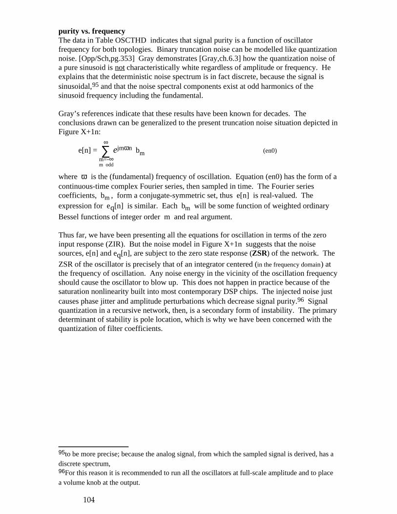
purity vs. frequencyThe data in Table OSCTHD indicates that signal purity is a function of oscillatorfrequency for both topologies. Binary truncation noise can be modelled like quantizationnoise. [Opp/Sch,pg.353] Gray demonstrates [Gray,ch.6.3] how the quantization noise ofa pure sinusoid is not characteristically white regardless of amplitude or frequency. Heexplains that the deterministic noise spectrum is in fact discrete, because the signal issinusoidal,95 and that the noise spectral components exist at odd harmonics of thesinusoid frequency including the fundamental.
Gray’s references indicate that these results have been known for decades. Theconclusions drawn can be generalized to the present truncation noise situation depicted inFigure X+1n:
e[n] = ejmωn bm (en0)∑m=-∞
∞
m odd
where ω is the (fundamental) frequency of oscillation. Equation (en0) has the form of acontinuous-time complex Fourier series, then sampled in time. The Fourier seriescoefficients, bm , form a conjugate-symmetric set, thus e[n] is real-valued. Theexpression for eq[n] is similar. Each bm will be some function of weighted ordinary
Bessel functions of integer order m and real argument.
Thus far, we have been presenting all the equations for oscillation in terms of the zeroinput response (ZIR). But the noise model in Figure X+1n suggests that the noisesources, e[n] and eq[n], are subject to the zero state response (ZSR) of the network. The
ZSR of the oscillator is precisely that of an integrator centered (in the frequency domain) atthe frequency of oscillation. Any noise energy in the vicinity of the oscillation frequencyshould cause the oscillator to blow up. This does not happen in practice because of thesaturation nonlinearity built into most contemporary DSP chips. The injected noise justcauses phase jitter and amplitude perturbations which decrease signal purity.96 Signalquantization in a recursive network, then, is a secondary form of instability. The primarydeterminant of stability is pole location, which is why we have been concerned with thequantization of filter coefficients.
95to be more precise; because the analog signal, from which the sampled signal is derived, has adiscrete spectrum,96For this reason it is recommended to run all the oscillators at full-scale amplitude and to placea volume knob at the output.
104

The data in Table OSCTHD suggests that either implementation of theoscillator/integrator has constant (noise equivalent)97 bandwidth, independent of centerfrequency. We intuit this because it appears that the quantity of noise goes up as centerfrequency moves down. Perhaps when the oscillation frequency is low, the morepowerful harmonics of the noise spectrum are clustered closer together in the vicinity ofthe center frequency. Hence the integrator becomes more disturbed, thus the THD+Nwill be worse. A simpler explanation might be frequency domain foldover of theintegrator transfer near DC.
chaotic behaviorThe direct form oscillator at 20 Hz is fascinating to view, however, when the signal pathbit-width is 20 bits (just before flatline). The oscillation metamorphoses from sinusoidal tonearly triangular, and back; this chaotic but stable process occurs over periods of realtime on the order of minutes. During each epoch, the oscillation frequency can beobserved to change by as much as 1/2 the desired frequency.
It should be pointed out that although we show no data for very low frequencies inTable OSCTHD, the first and second modified coupled form sinusoidal oscillators areroutinely called upon to produce frequencies less than 1 Hz (0.1 Hz typical).
97defined in [Harris] [Cooper]
105

More Recent DevelopmentsSmith and Cook subsequently disclosed a lattice topology for sustained oscillation in[Smith/Cook] which is claimed more suitable for VLSI implementation. The oscillatorshown in Figure SC is called the normalized waveguide oscillator because it wasderived as a spin-off from Smith’s results in the theory and implementation of digitalwaveguides.
y1[n+1] = cos(ωn) y1[n] + (cos(ωn)+1) Gn y2[n]
y2[n+1] = (cos(ωn)-1) y1[n] + cos(ωn) Gn y2[n]
Ζ-1 Ζ-1y2[n]
y1[n]
∑
∑
xx
Figure SC. Smith/Cook Normalized Waveguide Sinusoidal Oscillator.
∑
-
cos(ωn)Gn
y1[n+1]
y1[n] = y1[0] cos(n ωn) - y2G[0] cot(ωn/2) sin(n ωn)
y2[n] = y1[0] tan(ωn/2) sin(n ωn) + y2G[0] cos(n ωn)
Gn =tan(ωn/2)
tan(ωn-1/2); 0 < ωn < π/2 poles = cos(ωn) +/− j 1 - cos2(ωn)√
y2[n+1]
(oscSC)
106
Although this design recaptures the quadrature relationship of the sinusoids appearing atthe circuit outputs, the primary contribution of this topology to the field of oscillatordesign is that it solves the amplitude deviation problem.98 It is a remarkable distinctionthat this sinusoidal oscillator possesses: This normalized waveguide oscillator isdesigned for instantaneous change in frequency without concomitant change inamplitude,99 hence the new notation (ωn) showing frequency as a function of the time
index. The frequency change must be performed properly, however. Toward this end,the amplitude coefficient Gn is introduced, and specified to deviate from 1 only at the
time of the occurrence of the frequency change;100 i.e., it is an amplitude compensationfactor which is engaged for one sample period. The elegance of the Smith/Cook solutionrests in the fact that knowledge of the state time (the precise value of n) at the occurrenceis not required, neither is knowledge of the state values. All that is required is knowledgeof the previous frequency.
Whenever frequency is changed, the control Gn is all that is required to maintainconstant amplitude in the oscillator circuit; i.e., the memory elements need never beadjusted in the implementation. For the analytical equation (oscSC) to remain valid,however, y2G[0] and y1[0] must be re-evaluated whenever Gn deviates;
y1[0] <- y1[n0] y2G[0] <- y2[n0] Gn0
= y2G[n0] (oscG)
where n0 is the time index at the change; n0≠0. It is important that we interpret equation(oscSC) properly so that we may show the technique on paper. We will now demonstratethe validity of these assertions by example:
98It is evident from the equations in Figure SC that sinusoid amplitude is linked to thefrequency of oscillation. This is similar to the situation for all the oscillators presented, except forthe Rader/Gold coupled form.99Because we are dealing with the ZIR, frequency change can be instantaneous in all theoscillators presented. But the Smith/Cook oscillator is the first one to deal effectively withamplitude correction at the instant of the change.100 Gn is not at all involved with frequency tuning. The special case G0 = 1. But Gn can be
greater than 1, albeit momentarily, which will necessitate at least q22 arithmetic.
107

exampleSuppose that at absolute time n=0, we are given ω0=ω-1 , y1[0]=1, and y2G[0]=0.
Then while Gn remains static we expect for n = 0 -> ∞ ,
y1[n] = cos(n ω0) (osc0)
y2[n] = tan(ω0/2) sin(n ω0)
Suppose we suddenly freeze time at n=n0+ . At this time we desire a change infrequency which is effectively to take place at n=n0 . We do this by changing the one
tuning coefficient from cos(ω0) to cos(ωn0) at time n0 , and by letting Gn deviate
from 1 but only for one sample time at n0 ;
Gn0 = tan(ωn0
/2) / tan(ωn0-1/2) (oscG2)
We then have the new initial states from (osc0) and (oscG):ωn0-1 = ω0
y1[n0] = cos(n0 ωn0-1)
y2G[n0] = tan(ωn0/2) sin(n0 ωn0-1) (osc1)
Using the new initial states (osc1), we find from (oscSC) that, y1[n] = cos(n0 ωn0-1) cos((n-n0)ωn0
) - sin(n0 ωn0-1) sin((n-n0)ωn0)
y2[n] = cos(n0 ωn0-1) tan(ωn0/2) sin((n-n0)ωn0
) + tan(ωn0/2) sin(n0 ωn0-1) cos((n-n0)ωn0
)
;for n=n0 -> ∞ (osc2)Equation (osc2) simplifies by trigonometric identity to, y1[n] = cos(n0 ωn0-1 + (n-n0)ωn0
)
y2[n] = tan(ωn0/2) sin(n0 ωn0-1 + (n-n0)ωn0
) ;for n=n0 -> ∞ (osc3)
In both outputs the phase is correct in light of the new starting time. Comparing (osc3) to(osc0), we see that the amplitude of y1[n] remains as it was which is the desired result.To successfully change the frequency again and again, the same procedure can berepeated to derive similar results. But the amplitude of y2[n] has changed from its
original value of tan(ω0/2). So, in this particular example we have not maintained the
amplitude of y2[n] although we have managed to keep the amplitude of y1[n] constantthroughout the process of changing the frequency of oscillation.
It is interesting to note that Smith and Cook originally derived the same result usingprinciples of energy conservation across transformer-coupled waveguides.
108

stabilityThe Smith/Cook oscillator is hyperstable because there is only one tuning coefficient,cos(ωn). The equation for the poles in Figure SC shows that even under coefficient
quantization, the pole magnitude is always unity.101 Like the direct form, however, thesingle tuning coefficient requires high resolution at very low frequencies of oscillation.Inaccuracy in the representation of Gn when it deviates cannot affect the tuningfrequency.
truncation noiseWe will only permit speculation regarding the noise performance of the Smith/Cookoscillator as compared to the (Gordon/Smith) second modified coupled form, as we haveno actual measurements of THD+N to bolster any analytical findings.
Recalling our discussion ‘purity of direct vs. coupled form’, there the importance ofzeroes in the deterministic noise transfer function was revealed. We have not been ableto devise an implementation that would place a zero into the steady state truncation noisetransfer (amplitude coefficient Gn set to 1) while maintaining freedom from amplitude
deviation across a change in frequency.102
Hence we speculate that the noise performance of the Smith/Cook sinusoidal oscillator isnot as good as that of the Gordon/Smith.
miscellanySome other articles relevant to the field of oscillator design are [Fliege/Wintermantel] and[Thoen].
101Like the direct form, any instability in the sinusoidal waveform can only be attributed to signalquantization effects, primarily in the form of truncation error in this recursive topology. 102This topic is worthy of further research, however. One complicating circumstance is thepotentially large disparity in amplitude between the two outputs, as shown by (oscSC).
109
4. External Memory Host Access (Paradigm and Utility)The ESP2 does not provide direct access of external memory data by the system host atrun-time, nor during halt, nor suspension. We present here a typical scheme for vectoringa running ESP2 application to a simple utility program which makes the desired access atthe sample rate.103 The ESP2 acts as intermediary.
We create a new program paradigm for a sample-synchronous application beyond whichthe utility will be overlaid at run-time by a relocating downloader driven by the systemhost.104 We need a relocating downloader in order to select the start of the utilityanywhere within instruction memory.
We write the utility so that it needs to know as little as possible about the runningapplication. But we do need to know the relative address offset within the particularregion of external memory to which to begin access, and we need a few registers globallyreserved for the utility program. This information can be shared by all runningapplications, and we conveniently place it in an include file.
!************************* #include file.h contents ****************************DEFCONST GLOBAL
CLK = 40.e6 ! ESP2 system clock.
Fs = 44100. ! system sample rate.
T_LOCALE = $800000 ! fixed but arbitrary, agreed on by convention.
OVERLAY = 10 ! overlay-instruction budget .
AUDIO = 3*Fs ! 3 seconds. ESP_HALT = $2 ! see HOST_CNTL_SPR in Chip Spec.
DEFREGION T @T_LOCALE GLOBAL ! region desired for host/external memory transfer. capture[2*AUDIO] ! A few seconds of stereo audio.
sigmoid_table[257] ! Table used by a lot of programs. inverse_table[512] xmp @$2ff ! external memory pointer used by utility.
DEFGPR GLOBAL host_cntl_msk = ESP_HALT @$ff ! used to mask HOST_CNTL_SPR.
indirb @$fe ! used to save INDIRB of application.
!***********************************************************************
103Note that the elimination of the BIOZ instruction from the application program paradigm,presented shortly, would permit the host external memory access at a much higher rate.104The download, by the system host, of new instructions into ESP2 instruction memory alwaysoccurs at the instruction rate.
110

Resource ManagementWe assume that any DIL or DOL required by the utility’s AGEN operations will be freeat the instant that the utility is executed. This is a reasonable assumption and allowssharing of that resource.
The utility can use a few instructions in any unused instruction space. Recall that at asample rate of 44.1 kHz, only 226 ESP2 instruction lines can be executed per sampleperiod. So, there will likely be some instructions free that we will not need to take awayfrom the application resource.
We will reserve two GPRs; one to hold a semaphore mask (host_cntl_msk) and one to savethe application’s return address (indirb). Finally, we will need a dedicated and reservedAOR (xmp) which, together with the region BASEr, will point to the desired location inexternal memory. The AOR, xmp, is a relative address offset into the region, T in thiscase. It can be initialized, by the host, to the root address offset of any one of thedeclared external memory arrays. These three registers will only need to be initialized once throughout the use of the utility.
4.1. ESP2 External Memory Host Access Application Program Paradigm! JonD, ESP2, 1/1/95.
PROGRAM Transfer
#include file.h
PROGSIZE <= INT(CLK/(4.*Fs)) - OVERLAY !compensation for execute time, not size
DEFSPR LOCAL INDIRB = application PC = init REPT_CNT = 0 SER_CONF = $007fff ! see the Chip Spec. HARD_CONF = $008400
CODE!********************* begin application ***************************************init: NOP
.application: NOP ! JMP and return here
.
.
.NOP JMP INDIRECTNOP BIOZ
!******************* end application program ************************************
111

ProcedureWe assume that this application has been running for some time. The SPR INDIRBholds the PC value of the label called application as evidenced by the declarations. Thehost queries this register and saves its contents in the global GPR called indirb. The hosttakes the ESP_HALT_EN and ESP_HALT bits, of the HOST_CNTL interface register,low.
After the host overlays the utility, it overwrites INDIRB with the desired PC location ofthe start of the utility. When the JMP is encountered thereafter, it will be vectored to ourlittle utility. The host initializes the AOR, xmp, to the desired address offset into theregion T in external memory (see the chart in the Discussion).
When a semaphore is taken high by the host, the utility will be activated for a singlestereo access. The utility resets the semaphore. When the host is finished accessingexternal memory, it will set INDIRB back to its original contents thus bypassing theutility.
4.2. ESP2 External Memory Host Access Utility! JonD, ESP2, 1/2/95.
PROGRAM Utility
#include file.h
PROGSIZE <= OVERLAY
CODE!************************** begin WR utility *******************************utility:NOP AND host_cntl_msk, HOST_CNTL_SPR > ZERO
NOP JS push, NZ > CMR MOV indirb > PCSTACK0 ADDV host_cntl_msk, xmp
push:MOV HOST_GPR_DATA > *xmp(+) RS, NZ > CMR MOV HOST_ESP_FACE > *xmp XOR host_cntl_msk, HOST_CNTL_SPR!**************************** end utility **********************************
112

Discussion of UtilityThe JS in conjunction with the load of PCSTACK0 constitutes a push of indirb onto thehardware stack. The GPR, indirb, holds the PC value of the label application, and wasloaded by the system host during initialization of this procedure. This is done so that RSwill know where to return to within the application. JS and RS each have one instructioncycle execution latency, and they are unconditionally executed. This little utility is calledat the sample rate as part of the running application which is never stalled.
The only unconventional usage within the utility is of HOST_CNTL_SPR. This registeris unusual in so far as it appears simultaneously in the host interface register space (asHOST_CNTL) and in the ESP2 SPR space. This fact makes that register desirable forfast inter-communication. We sacrifice one of the bits of that register, namely theESP_HALT bit, for use as the semaphore. This is possible if the host holds theESP_HALT_EN bit low and if we agree that there are no HALT pseudo instructions,within the application, that we need activated during this time.
The HOST_GPR_DATA and HOST_ESP_FACE SPRs are the only other registerssharing the attribute of simultaneous appearance in the SPR and host interface registerspaces. This design yields the ultimate speed in register data transfer because the hostdoes not need to go through the standard host/ESP2-register interface to transfer datasomewhere that the ESP2 can see it directly; namely, from/to these two SPRs. Thismeans that there is no need for the execution of BIOZ or HOST instructions in order thatthe host be able to communicate with a running ESP2 program via these three registers;and vice versa.105
The HOST_ESP_FACE SPR is uncommitted, but the HOST_GPR_DATA SPR is anintegral part of the host interface for internal register access. We employ both theseregisters in our utility because we want stereo data access. Use of HOST_GPR_DATAhere does not preclude standard use of the host/ESP2-register interface, however; this isbecause of the semaphore protocol.
As shown, the utility writes stereo data out to external memory. The stereo data arepresumed stored in an interleaved fashion (Left channel, Right channel, Left...), so weemploy to our advantage the AGEN’s Plus-One addressing mode (+). The twoconditional external memory WR are scheduled on the same respective instruction linesin the AGEN as the lines of requesting MAC code.106 This means that the scheduledconditional AGEN code experiences the same CCR and CMR as the requesting MACcode.
105Therefore, we could eliminate the synchronization of this utility to the BIOZ suspension in theapplication program so that external memory data transfer would exceed the sample rate.106We could insure this via the assembler’s forced WR directive, => , but that is not necessaryfor these isolated five lines because there is little external memory traffic.
113

The GPR, host_cntl_msk, performs double duty as a semaphore mask and as theincrement for our stereo data pointer, the AOR called xmp. The increment to xmp willbecome effective for the second current external memory WR because of the assemblerscheduling in the AGEN.
All four last lines of code in the utility, in fact, see the same CCR and CMR. For thisreason, the utility doubles for both RD and WR access. To make the utility perform RDaccess, the source and destination in each of the last two lines of MAC unit code areinterchanged. Because of the scheduling, in that case, xmp will not increment in time toaffect the two current external memory RD in the AGEN.
Given these considerations we have the following chart for the proper use of this utility:
HOST_GPR_DATA HOST_ESP_FACE xmp initializationWR Left channel data Right channel data address offset - 1RD Right channel data Left channel data address offset
There is a potential hazard with the host interface when using either of these two SPRsas MAC unit destination in the RD utility. This hazard comes about because of eachSPRs’ simultaneous appearance in two register spaces. Once again, the hazard is avoidedby the semaphore protocol; the conditionally executed instructions inhibit the destinationunless the semaphore bit is high. Notice the efficiency we have gained through the use ofconditionally executable code, denoted by . Without it, we would have the overhead ofjumping around it.
114

5. FFT Radix-4
5.1. FFT Radix-4 C-Program Model/* This is a validation test of the [Burrus/Parks,pg.113] Radix-4 FFT - JonD 1/15/93 */
/* This is an in-place algorithm. */
/* Modified for zero-indexing. */
#include <stdio.h>
#include <math h>
#define FREQ 4 /* power of two < 64, to get integral period */
/* and to keep epsilon q23 */
#define N 256
#define RADIX 4
#define TWIDDLE_SIZE 2*N
double roundint();
double pow2to23, RoundInt24(), TruncInt24();
void main()
/* FFT */
int N1, N2, M, IE, IA1, IA2, IA3, I1, I2, I3, I, J, K;
long templ;
double CO1, CO2, CO3, SI1, SI2, SI3, XT, YT, R1, R2, R3, R4, S1, S2, S3, S4;
double R1b, R2b, R3b, S1b, S2b, S3b;
double X[N], Y[N];
/* TWIDDLE */
double twopi, Wreal[N], Wimag[N];
/* INPUT SIGNAL */
double epsilon, yn, yqn;
double pi;
/* init */
M = roundint(log((double)N)/log((double)RADIX));
twopi = 8.*atan(1.);
pi = 4.*atan(1.);
pow2to23 = pow(2.0, 23.0);
115

/**************** GENERATE TWIDDLE FACTORS ***************/
/* first value is: 0x7FFFFF */ /* first interleaved value is: 0x000000 */
/* last value is: 0x7FF622 */ /* last interleaved value is: 0xFCDBD5 */
printf("Twiddle factor table size is: %d\n", TWIDDLE_SIZE);
/*for(K=0; K<N; K++)
Wreal[K] = RoundInt24(cos((K*twopi)/N));
templ = pow2to23*Wreal[K];
if(templ >= 0x00800000L)
Wreal[K] = TruncInt24(1.0 - pow(2., -23.));
templ = 0x7fffffL;
printf("%0.6lx\n", templ & 0xffffffL);
Wimag[K] = RoundInt24(sin((K*twopi)/N));
templ = pow2to23*Wimag[K];
if(templ >= 0x00800000L)
Wimag[K] = TruncInt24(1.0 - pow(2., -23.));
templ = 0x7fffffL;
printf("%0.6lx\n", templ & 0xffffffL);
*/ /* 24-bit fixed-point, q23 */
for(K=0; K<N; K++) /* floating-point */
Wreal[K] = cos((K*twopi)/N);
Wimag[K] = sin((K*twopi)/N);
/*************** end TWIDDLE *********************************/
/*** GENERATE INPUT SIGNAL ********************************/
epsilon = 2.*sin((pi*FREQ)/N);
yqn = 0.0;
yn = -cos((pi*FREQ)/N);
for(K=0; K<N; K++)
X[K] = yqn/2.; /* fixed-point overflow prevention */
Y[K] = 0.0/2.;
yqn -= epsilon*yn;
yn += epsilon*yqn;
/*************** end INPUT *********************************/
/*
for(I=0; I<N; I++)
printf("X[%d] = %lf\t Y[%d] = %lf\n", I, X[I], I, Y[I]);
*/
116
/********************* THE FFT *******************************/
N2 = N;
IE = 1;
for(K=0; K<M; K++)
N1 = N2;
N2 = N2 >> 2;
IA1 = IA2 = IA3 = 0;
for(J=0; J<N2; J++)
CO1 = Wreal[IA1];
CO2 = Wreal[IA2];
CO3 = Wreal[IA3];
SI1 = Wimag[IA1];
SI2 = Wimag[IA2];
SI3 = Wimag[IA3];
I1 = J + N2;
I2 = I1 + N2;
I3 = I2 + N2;
for(I=J; I<N; I+=N1)
R1 = (X[I] + X[I2])/(RADIX/2);
R3 = (X[I] - R1);
S1 = (Y[I] + Y[I2])/(RADIX/2);
S3 = (Y[I] - S1);
R2 = (X[I1] + X[I3])/(RADIX/2);
R4 = (X[I1] - R2);
S2 = (Y[I1] + Y[I3])/(RADIX/2);
S4 = (Y[I1] - S2);
R2b = R1 - R2;
S2b = S1 - S2;
R1b = R3 - S4;
S1b = S3 + R4;
R3b = R3 + S4;
S3b = S3 - R4;
X[I2] = (CO2*R2b + SI2*S2b)/(RADIX/2);
Y[I2] = (CO2*S2b - SI2*R2b)/(RADIX/2);
X[I3] = (CO3*R1b + SI3*S1b)/(RADIX/2);
Y[I3] = (CO3*S1b - SI3*R1b)/(RADIX/2);
X[I1] = (CO1*R3b + SI1*S3b)/(RADIX/2);
Y[I1] = (CO1*S3b - SI1*R3b)/(RADIX/2);
X[I] = (R1 + R2)/(RADIX/2);
Y[I] = (S1 + S2)/(RADIX/2);
I1 += N1;
I2 += N1;
I3 += N1;
IA1 += IE;
IA2 = IA1 + IA1;
IA3 = IA2 + IA1;
IE = IE << 2;
/************** end FFT *****************/
117

/******************** Digit Reversal Address/Input Scaling Compensation *******/
J = 0;
N1 = N - 1;
for(I=0; I<N1; I++)
if(I >= J) goto label101;
XT = X[J];
X[J] = X[I];
X[I] = XT;
YT = Y[J];
Y[J] = Y[I];
Y[I] = YT;
label101: K = N/RADIX;
label102: if(K*3 > J) goto label103;
J = J - K*3;
K /= RADIX;
goto label102;
label103: J += K;
for(I=0; I<N; I++) /* compensation for earlier fixed-point overflow prevention */
X[I] *= 2.;
Y[I] *= 2.;
/*********************************** end BIT SWAP ****************/
for(I=0; I<N; I++)
if((fabs(X[I]) >= 1e-16) || (fabs(Y[I]) >= 1e-16))
printf("X[%d] = %.16lf\t Y[%d] = %.16lf\n", I, X[I], I, Y[I]);
/******************** subroutines ***********************************/
/******** replacement for rint() on NeXT O.S. v2.1 *******/
double roundint(double x)
if(x >= 0.)return((double)((int)(x + 0.5)));
return((double)((int)(x - 0.5)));
double TruncInt24(x)
double x;
return(floor(pow2to23*x)/pow2to23);
double RoundInt24(x)
double x;
return(roundint(pow2to23*x)/pow2to23);
118

5.2. FFT Radix-4 ESP2 Program! FFT Radix-4, single precision. - JonD February 18, ’93 .
! 53 ESP2 instructions. 1024 point complex input @3.245 ms @10 MHz instruction rate.
! Execution 7 times faster than real time @Fs = 44100 Hz.
! THD+N = approx 110 dB regardless of input signal amplitude @ normalized frequency = 4/N .
! Butterflys are scaled so that FFT of full-scale sinusoid produces +/- $400000
! System host must set the ESP_HALT_EN bit of the HOST_CNTL interface register.
PROGRAM FFT4
PROGSIZE = 64 ! - 11
DEFCONST
XI = #DILF YI3 = #DIL8
XI2 = #DILE CO1 = #DIL7
YI = #DILD CO2 = #DIL6
YI2 = #DILC CO3 = #DIL5
XI1 = #DILB SI1 = #DIL4
XI3 = #DILA SI2 = #DIL3
YI1 = #DIL9 SI3 = #DIL2
RADIX = 4
N = 256 ! can’t be 128
M = INT(LOG(N)/LOG(RADIX))
FREQ = 4
Pi = 4.0*ATAN(1.0)
EPSILON = 2.0*SIN((Pi*FREQ)/N)
BIG_ONE = (2**24)/N
REGION_R_LOC = $800000
REGION_I_LOC = $800400 REGION_T_LOC = $800800
DEFSPR PC = begin
REPT_CNT = 0 DILA DILB DILC DILE DILF SER_CONF = $007fff DIL6 DIL7 DIL8 DIL9 HARD_CONF = $008400 DIL2 DIL3 DIL4 DIL5
DEFGPR
GLOBAL
epsilon = EPSILON
yqn = 0
yn = -COS((Pi*FREQ)/N)
LOCAL
J IE R1 R2 R3 R4 S1 S2 S3 S4 R1b R2b R3b S1b S2b S3b
N2 count
Irev IA1 IA2 IA3
119

DEFREGION T @REGION_T_LOC ! TABLE REGION
Twiddle[2*N] ! holds interleaved single precision (cos(), sin()) table;
! loaded by system host at download. 0 root required.
IA1_doub ! AORs
IA2_doub
IA3_doub
DEFREGION R @REGION_R_LOC ! DELAYLINE REGION
XinArray[N] ! real input, single precision, q23. 0 root required.
Xoutput[N] ! output array, q23. Loaded post digit-reversal.
XoutPointer
RevPointer ! digit reverse pointer.
K @$2f9 ! default region is R; used in region I
I I1 N1 ! don’t init any AORs to 0; confusion later with XinArray[0]
I2 I3
Ir I1r ! to avoid wasting another 2 regions
I2r I3r
DEFREGION I @REGION_I_LOC
YinArray[N] ! imaginary input, q23. 0 root required.
Youtput[N] ! output array, q23. Loaded post digit-reversal.
! Must be in same relative position as Xoutput[N]
!********************** END declarations *****************************************!
CODE
!******************** generate input signal *****************************!
begin: CLR K CLR I
!*** initialize input arrays ***
signal_loop: CLR *(K)I HALVE yqn > *(K)R !overflow prevention in first butterfly
!****** hyperstable near-quadrature oscillator (second modified coupled form) ******
MOV yqn > MACP MOV yn > MACP
MACP - epsilon X yn > yqn
MACP + epsilon X yqn > yn !*** end oscillator ***
!*** go around loop simple way ***
NOP ADDV ONE, K
NOP CMP K, #N
NOP JMP signal_loop, NEQ > CMR
NOP
!******************************** end input signal generation ************!
120

!************************** begin the FFT ********************************
fft: MOV ONE > IE MOV #N > N2
MOV #REGION_R_LOC > BASER CLR K
K_loop:MOV N2 > N1 CLR IA1
CLR J LSH N2 >>2
CLR IA2 CLR IA3
J_loop:
MOV N2 > MACP MOV #REGION_I_LOC > BASEI
ADD N2, MACP > I2 ADDV J, BASEI RD *(I )R > XI !XinArray
ADD I2, MACP > I3 MOV N2 > I1 RD *(I2)R > XI2
NEG ONE > MACP SUBV N1, SIZEM1R > MACP RD *(I )I > YI !YinArray
ADD IE, MACP > count AVG XI, XI2 > R1 RD *(I2)I > YI2
ADD ONE, MACP SUB R1, XI > R3 RD *(I1)R > XI1
NOP AVG YI, YI2 > S1 RD *(I3)R > XI3
NOP SUB S1, YI > S3 RD *(I1)I > YI1
DBL IA2 > IA2_doub AVG XI1, XI3 > R2 RD *(I3)I > YI3
DBL IA3 > IA3_doub SUB R2, XI1 > R4 RD *(IA2_doub) > CO2
DBL IA1 > IA1_doub AVG YI1, YI3 > S2 RD *(IA2_doub(+)) > SI2
NOP SUB S2, YI1 > S4 RD *(IA3_doub) > CO3
NOP SUB R2, R1 > R2b RD *(IA3_doub(+)) > SI3
NOP SUB S2, S1 > S2b RD *(IA1_doub) > CO1
ADD I, MACP > Ir SUB S4, R3 > R1b RD *(IA1_doub(+)) > SI1
ADD I1, MACP > I1r ADD S3, R4 > S1b RD *(BASE += N1)R > XI !ok
ADD I2, MACP > I2r ADD R3, S4 > R3b RD *(I2)R > XI2
ADD I3, MACP > I3r SUB R4, S3 > S3b RD *(BASE += N1)I > YI !ok
NOP REPT I_loopEnd, count > REPT_CNT
I_loop:
R2b X CO2 > MAC AVG R1, R2 > *(Ir)R RD *(I2)I > YI2
MAC + S2b X SI2 >>1 > *(I2r)R AVG S1, S2 > *(Ir)I RD *(I1)R > XI1
S2b X CO2 > MAC AVG XI, XI2 > R1 RD *(I3)R > XI3
MAC - R2b X SI2 >>1 > *(I2r)I SUB R1, XI > R3 RD *(I1)I > YI1
R1b X CO3 > MAC AVG YI, YI2 > S1 RD *(I3)I > YI3
MAC + S1b X SI3 >>1 > *(I3r)R SUB S1, YI > S3
S1b X CO3 > MAC AVG XI1, XI3 > R2
MAC - R1b X SI3 >>1 > *(I3r)I SUB R2, XI1 > R4
R3b X CO1 > MAC AVG YI1, YI3 > S2
MAC + S3b X SI1 >>1 > *(I1r)R SUB S2, YI1 > S4
S3b X CO1 > MAC SUB R2, R1 > R2b
MAC - R3b X SI1 >>1 > *(I1r)I SUB S2, S1 > S2b
NOP SUB S4, R3 > R1b
NOP ADD S3, R4 > S1b RD *(BASE += N1)R > XI
NOP ADD R3, S4 > R3b RD *(I2)R > XI2
I_loopEnd:NOP SUB R4, S3 > S3b RD *(BASE += N1)I > YI
121

MOV IA1 > MACP ADDV ONE, J
ADD IE, MACP > MAC, IA1 CMP J, N2
SHIFTMAC <<1 > IA2 JMP J_loop, LT > CMR
ADD IA2, MAC > IA3 ADDV J, #REGION_R_LOC > BASER
MOV #REGION_R_LOC > BASER CMP K, #M-1
ASH IE <<2 JMP K_loop, LT > CMR
MOV #REGION_I_LOC > BASEI ADDV ONE, K
!************* digit reversal / undo overflow prevention in first butterfly **********************!
MOV &XinArray[0] > RevPointer MOV &Xoutput[0] > XoutPointer
CLR Irev REPT reversal, N-1
NOP ADDV #BIG_ONE, Irev RD *(RevPointer)R > XI
NOP DREV Irev > RevPointer RD *(RevPointer)I > XI2
DBL XI => *(XoutPointer)R
reversal: DBL XI2 => *(XoutPointer)I ADDV ONE, XoutPointer
!******************************* end digit rev ************************************!
!*************************** end FFT ************************************!
NOP HALT
NOP
!*******************************************************************************!
122
5.3. FFT Radix-4 C-Program Simulation of ESP2 Program
/* reference file: fft4.c */
/* cd /jond/esp2/Csource */
/* This is a single precision fixed point (48-bit) rendering for ESP2 simulation. -Jon Dattorro 1993 */
/* Each stage of butterflies is scaled by 4 to prevent overflow. A sinusoid
will then have standard power level as output from scaled DFT (scaled by factor N).
The complex input signal is stored in a single precision array.
*/
#include <stdio.h>
#include <math.h>
double pow(), atan(), log(), log10(), sin(), cos(), sqrt(), floor();
double pow2to46, select_lower24(), lower24();
double pow2to47, RoundInt48(), TruncInt48(), TruncInt48MAC();
double pow2to23, RoundInt24(), TruncInt24();
double pow2to15, TruncInt16(), RoundInt16(), roundint();
double myfmod();
#define NMAX 4096
#define FREQ 4 /* integer, empirical value. Period is always N/FREQ */
#define RADIX 4
#define TWIDDLE_LOC 0x0
#define TWIDDLE_SIZE 2*N
void main()
/* FFT */
char buf[32];
int N1, N2, M, IE, J, K, N;
int I, I1, I2, I3, IA1, IA2, IA3;
double CO1, SI1, CO2, SI2, CO3, SI3;
double R1, R2, R3, R4, S1, S2, S3, S4;
double R2b, R3b, R1b, S2b, S3b, S1b;
double X[NMAX], Y[NMAX], preswapX[NMAX], preswapY[NMAX], XT;
double noise_power;
/* TWIDDLE */
long templ;
double twopi, WR[NMAX], WI[NMAX];
/* INPUT SIGNAL */
double pi, amplitude, sinamp, sinamp_dB;
123
/*printf("Input number of points: ");
gets(buf); sscanf(buf, "%d", &N);
printf("Input amplitude of sinusoid (0. -> -90. dB): ");
gets(buf); sscanf(buf, "%lf", &sinamp_dB);
sinamp = pow(10., sinamp_dB/20.);
*/
sinamp = 1.0;
N = 256;
M = roundint(log((double)N)/log((double)RADIX));
twopi = 8.*atan(1.);
pi = 4.*atan(1.);
pow2to47 = pow(2.0, 47.0);
pow2to46 = pow(2.0, 46.0);
pow2to23 = pow(2.0, 23.0);
pow2to15 = pow(2.0, 15.0);
/**************** GENERATE TWIDDLE FACTORS ********************************/
/*printf("%0.6lx\t\t", TWIDDLE_LOC);*/
/*printf("%d\n", TWIDDLE_SIZE);*/
for(K=0; K<N; K++)
WR[K] = RoundInt24(cos((K*twopi)/N));
templ = pow2to23*WR[K];
if(templ >= 0x00800000L)
WR[K] = TruncInt24(1.0 - pow(2., -23.));
templ = 0x7fffffL;
/*printf("%0.6lx\n", templ & 0xffffffL);*/ /* redirect std output to get */
/* ascii file */
WI[K] = RoundInt24(sin((K*twopi)/N));
templ = pow2to23*WI[K];
if(templ >= 0x00800000L)
WI[K] = TruncInt24(1.0 - pow(2., -23.));
templ = 0x7fffffL;
/*printf("%0.6lx\n", templ & 0xffffffL);*/
/*************** end TWIDDLE *********************************/
124

/*** GENERATE INPUT SIGNAL ********************************/
amplitude = (pow2to23-1.)/pow2to23;
for(K=0; K<N; K++)
X[K] = TruncInt24(0.5*sinamp*amplitude*sin(myfmod((twopi*FREQ*K)/N, twopi)));/* scale ovf in 1st butterfly.*/
Y[K] = 0.0; /* Use of RountInt yields better S/N */
/* printf("%0.6lx\n", (long)(pow2to23*X[K]) & 0xffffffL);*/ /* redirect std output to get */
/* ascii file */
/*************** end INPUT *********************************/
/********************* THE FFT *******************************/
N2 = N;
IE = 1;
for(K=0; K<M; K++)
N1 = N2;
N2 = N2 >> 2;
IA1 = IA2 = IA3 = 0;
for(J=0; J<N2; J++)
CO1 = WR[IA1];
CO2 = WR[IA2];
CO3 = WR[IA3];
SI1 = WI[IA1];
SI2 = WI[IA2];
SI3 = WI[IA3];
I1 = J + N2;
I2 = I1 + N2;
I3 = I2 + N2;
for(I=J; I<N; I+=N1)
R1 = TruncInt24((X[I] + X[I2])/(RADIX/2)); /* scale by 4 for */
R3 = TruncInt24(X[I] - R1); /* each */
S1 = TruncInt24((Y[I] + Y[I2])/(RADIX/2)); /* stage of */
S3 = TruncInt24(Y[I] - S1); /* butterflies */
R2 = TruncInt24((X[I1] + X[I3])/(RADIX/2));
R4 = TruncInt24(X[I1] - R2);
S2 = TruncInt24((Y[I1] + Y[I3])/(RADIX/2));
S4 = TruncInt24(Y[I1] - S2);
R2b = TruncInt24(R1 - R2);
S2b = TruncInt24(S1 - S2);
R1b = TruncInt24(R3 - S4);
S1b = TruncInt24(R4 + S3);
R3b = TruncInt24(S4 + R3);
S3b = TruncInt24(S3 - R4);
125
/* if (K == 1)
printf("x[%d] = %lx x[%d] = %lx x[%d] = %lx x[%d] = %lx\n",I,(int)floor(pow2to23*X[I]),
I1,(int)floor(pow2to23*X[I1]),I2,(int)floor(pow2to23*X[I2]),I3,(int)floor(pow2to23*X[I3]));
printf("y[%d] = %lx y[%d] = %lx y[%d] = %lx y[%d] = %lx\n",I,(int)floor(pow2to23*Y[I]),
I1,(int)floor(pow2to23*Y[I1]),I2,(int)floor(pow2to23*Y[I2]),I3,(int)floor(pow2to23*Y[I3]));
*/
X[I2] = TruncInt24((TruncInt48MAC(CO2*R2b) + TruncInt48MAC(SI2*S2b))/(RADIX/2));
Y[I2] = TruncInt24((TruncInt48MAC(CO2*S2b) - TruncInt48MAC(SI2*R2b))/(RADIX/2));
X[I3] = TruncInt24((TruncInt48MAC(CO3*R1b) + TruncInt48MAC(SI3*S1b))/(RADIX/2));
Y[I3] = TruncInt24((TruncInt48MAC(CO3*S1b) - TruncInt48MAC(SI3*R1b))/(RADIX/2));
X[I1] = TruncInt24((TruncInt48MAC(CO1*R3b) + TruncInt48MAC(SI1*S3b))/(RADIX/2));
Y[I1] = TruncInt24((TruncInt48MAC(CO1*S3b) - TruncInt48MAC(SI1*R3b))/(RADIX/2));
X[I ] = TruncInt24((R1 + R2)/(RADIX/2));
Y[I ] = TruncInt24((S1 + S2)/(RADIX/2));
/* if (K == 1)
printf("xout[%d] = %lx xout[%d] = %lx xout[%d] = %lx xout[%d] = %lx\n",I,(int)floor(pow2to23*X[I]),
I1,(int)floor(pow2to23*X[I1]),I2,(int)floor(pow2to23*X[I2]),I3,(int)floor(pow2to23*X[I3]));
printf("yout[%d] = %lx yout[%d] = %lx yout[%d] = %lx yout[%d] = %lx\n",I,(int)floor(pow2to23*Y[I]),
I1,(int)floor(pow2to23*Y[I1]),I2,(int)floor(pow2to23*Y[I2]),I3,(int)floor(pow2to23*Y[I3]));
*/ I1 += N1;
I2 += N1;
I3 += N1;
IA1 += IE;
IA2 = IA1 + IA1;
IA3 = IA2 + IA1;
IE = IE << 2;
/************************************ end FFT *********************/
for(I=0;I<N;I++)
preswapX[I] = X[I];
preswapY[I] = Y[I];
126

/********************** BIT SWAP/INPUT SCALING COMPENSATION *******/
J = 0;
N1 = N - 1;
for(I=0; I<N1; I++)
if(I >= J) goto label101;
XT = X[J];
X[J] = X[I];
X[I] = XT;
XT = Y[J];
Y[J] = Y[I];
Y[I] = XT;
label101:K = N/RADIX;
label102:if(K*3 > J) goto label103;
J -= K*3;
K /= RADIX;
goto label102;
label103:J += K;
for(I=0; I<N; I++)
X[I] *= 2.;
Y[I] *= 2.;
/*********************************** end BIT SWAP ****************/
/**************************************** STATISTICS *********************/
noise_power = 0;
for(I=0; I<N; I++)
if((fabs(X[I]) < pow(2., -23.)) && (fabs(Y[I]) < pow(2., -23.)));
else
printf("X[%d] = %.16f\t Y[%d] = %.16f\n", I, X[I], I, Y[I]);
templ = floor(X[I]*pow2to23);
printf("integerX = %x\t\t\t", templ & 0xfffffeL);
templ = floor(Y[I]*pow2to23);
printf(" integerY = %x\n", templ & 0xfffffeL);
if((I == FREQ) || (I == (N-FREQ))) /* sine (not cosine) wave is assumed */
noise_power += X[I]*X[I];
else noise_power += X[I]*X[I] + Y[I]*Y[I];
noise_power += pow((0.5*amplitude*sinamp + Y[FREQ]), 2.) + pow((0.5*amplitude*sinamp - Y[N-FREQ]), 2.);
printf("signal/noise w/r full scale is: %.13f dB\n", -10.*log10(noise_power/(0.5*amplitude*amplitude)));
/*********************************************************************/
127

for(I=0; I<N; I++)
/* templ = floor(preswapX[I]*pow2to23);
printf("integerX[%d] = %x\t\t\t",I, templ & 0xffffffL);
templ = floor(preswapY[I]*pow2to23);
printf(" integerY[%d] = %x\n",I+513, templ & 0xffffffL);
templ = floor(X[I]*pow2to23);
printf("integerX[%d] = %x\t\t\t",I, templ & 0xffffffL);
templ = floor(Y[I]*pow2to23);
printf(" integerY[%d] = %x\n",I, templ & 0xffffffL);
*/
/************************************************************************************************************/
/****************************** SUBROUTINES *****************************/
double RoundInt48(x)
double x;
return(roundint(pow2to47*x)/pow2to47);
double RoundInt24(x)
double x;
return(roundint(pow2to23*x)/pow2to23);
double RoundInt16(x)
double x;
return(roundint(pow2to15*x)/pow2to15);
double TruncInt48(x)
double x;
return(floor(pow2to47*x)/pow2to47);
double roundint(double x) /*** replacement for rint() ***/
if(x >= 0.)return((double)((int)(x + 0.5)));
return((double)((int)(x - 0.5)));
128
double TruncInt48MAC(x)
double x;
return(floor(pow2to46*x)/pow2to46);
double TruncInt24(x) /* This emulates initialization in esp2 assembler */
double x;
return(floor(pow2to23*x)/pow2to23);
double TruncInt16(x)
double x;
return(floor(pow2to15*x)/pow2to15);
double select_lower24(x) /* also loses the LSB; the 48th bit */
double x;
double TruncInt24(), tempd;
tempd = x - TruncInt24(x);
return(floor(pow2to46*tempd)/pow2to46);
double lower24(x)
double x;
double TruncInt24(), tempd;
tempd = x - TruncInt24(x);
return(floor(pow2to47*tempd));
/****************** MYFMOD function ********************************************/
/*** used to increase accuracy of sin routines ***/
/*** fmod() uses floor() instead of (int). ***/
/*** fmod() also failing to return values within |modulo| ***/
/*** Want (int), which is magnitude truncation, for negative arguments. ***/
double myfmod(argument, modulo)
register double argument, modulo;
return(argument - (int)(argument/modulo)*modulo);
/********************************* END subroutines *****************************/
129

5.4. Comments on the FFT Radix-4 ProgramThe Twiddle factor [Opp/Sch] [AnalogDevices] table must be loaded into externalmemory before the ESP2 program is run. To load external memory, another ESP2Application must be run. See the External Memory Host Access Application. The Ccode for the Twiddle factor table generation is given within the C-program model for theFFT itself. The complex Twiddle factor table is interleaved; cosine then sine, cosine,sine, etc. This is done so as to use to advantage the AGEN’s automatic Plus-Oneaddressing mode (+). As a check, the C-program comments include the values of the firstand last interleaved Twiddle factors.
Notice that in many instances, the programmer has chosen to explicitly write the AGENcode. The programmer has also managed to give the various DILs meaningful namesthrough a DEFCONST declaration. It is important to declare those DILs in a DEFSPR sothat the assembler relinquish those particular resources. If the programmer has designedthe algorithm so that those DILs are free when the assembler might need them, then thedeclaration might be unnecessary.
The FFT portion of the ESP2 program is a translation of the C-program model. Theseparate C-program simulation estimates the S/N (signal to noise power ratio) of this singleprecision FFT Radix-4 circuit itself to be in excess of 110 dB as implemented within theESP2.107
The conventional DFT (Discrete Fourier Transform [ibid.]) inherently amplifies all signals by afactor N, the DFT length. The conventional IDFT (Inverse DFT) must scale all the binvalues by 1/N to recover the original input signal. In the algorithms108 that we present,the responsibility of scaling is transferred to the FFT because of a high likelihood of binoverflow when using a fixed-point processor. The scaling of the complex input signal isdistributed over each stage of butterflys to minimize truncation noise. This successivescaling yields a remarkable robustness, even for low-level input signals.
Another approach to scaling employs the block floating-point technique which can beimplemented within a fixed-point processor, such as ESP2, having barrel shifters. Thistechnique performs a signal-dependent scaling. [ibid.] [Kim/Sung]
107The sinusoid frequency used in the estimate is centered on an FFT bin frequency. [ibid.]Using an irrational frequency should not change the total noise power, but it will impact thecharacter of the noise power spectrum.108The FFT algorithm, in general, is simply a faster DFT. (But not fast enough!)
130

5.5. Changes Required to ESP2 Program to make the IFFT(Radix-4)
Complex SwapWe would like the simplest conversion possible; this means using the same Twiddlefactor table. We will use a DSP trick; define the swap operation on the real andimaginary parts of a complex quantity:
swap(z) = j z* = y + j x ; z = x + j y, j = √-1The asterisk denotes complex conjugation. Then, using the classical definitions of thetransform pair,
IDFTX[k] = ( j / N) ( DFT j X*[k] )*
= swap( ( 1 / N) DFTswap(X[k]) )The proof of this follows from the fact that we can show that
IDFTX[k] = (1 / N) ( DFTX*[k] )*
This means that to get an IFFT (Inverse FFT) using an FFT algorithm, one must first swapthe real and imaginary parts of the complex input record. After the swapped input haspassed through the FFT, we then simply swap the complex parts of the FFT output to getthe desired result.
Remove ScalingThe required modification to our FFT algorithm, for conversion to the IFFT, is toeliminate the scaling at each butterfly stage in the program core. Recall that the classical definition of the discrete transform pair [Opp/Sch,pg.532] showsscaling by 1/N appearing in only the IDFT. We previously decided to put the scaling intothe FFT algorithm instead, because the classical DFT of a real full-scale sampled sinusoidcan produce a bin output magnitude as high as N/2. Any value whose magnitude isbeyond 1.0 cannot be represented in the q23 output format we have chosen for the FFTimplementation. Because of the scaling, however, any full-amplitude sinusoid can berepresented in our FFT.
Because the first stage of butterflys is topologically prior to scaling, we always cut theinput signal amplitude by 1/2 before passing it on to the FFT algorithm. We do this toprevent overflow in the first stage of butterflys. Likewise for the IFFT; even though thereis no required scaling following our butterfly stages, the possibility of overflow stillexists in the first butterfly of our IFFT. So, the input amplitude halving and itsconcomitant post-digit-reversal amplitude compensation remains in both the FFT andIFFT algorithms.
This swapping is not constituent to the core of the IFFT algorithm that follows. Therequired changes with regard to scaling by (1/N) appear in bold type:
131
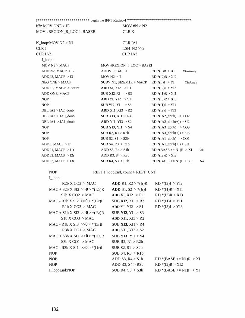
!************************** begin the IFFT Radix-4 ********************************
ifft: MOV ONE > IE MOV #N > N2
MOV #REGION_R_LOC > BASER CLR K
K_loop:MOV N2 > N1 CLR IA1
CLR J LSH N2 >>2
CLR IA2 CLR IA3
J_loop:
MOV N2 > MACP MOV #REGION_I_LOC > BASEI
ADD N2, MACP > I2 ADDV J, BASEI RD *(I )R > XI !XinArray
ADD I2, MACP > I3 MOV N2 > I1 RD *(I2)R > XI2
NEG ONE > MACP SUBV N1, SIZEM1R > MACP RD *(I )I > YI !YinArray
ADD IE, MACP > count ADD XI, XI2 > R1 RD *(I2)I > YI2
ADD ONE, MACP SUB XI2, XI > R3 RD *(I1)R > XI1
NOP ADD YI, YI2 > S1 RD *(I3)R > XI3
NOP SUB YI2, YI > S3 RD *(I1)I > YI1
DBL IA2 > IA2_doub ADD XI1, XI3 > R2 RD *(I3)I > YI3
DBL IA3 > IA3_doub SUB XI3, XI1 > R4 RD *(IA2_doub) > CO2
DBL IA1 > IA1_doub ADD YI1, YI3 > S2 RD *(IA2_doub(+)) > SI2
NOP SUB YI3, YI1 > S4 RD *(IA3_doub) > CO3
NOP SUB R2, R1 > R2b RD *(IA3_doub(+)) > SI3
NOP SUB S2, S1 > S2b RD *(IA1_doub) > CO1
ADD I, MACP > Ir SUB S4, R3 > R1b RD *(IA1_doub(+)) > SI1
ADD I1, MACP > I1r ADD S3, R4 > S1b RD *(BASE += N1)R > XI !ok
ADD I2, MACP > I2r ADD R3, S4 > R3b RD *(I2)R > XI2
ADD I3, MACP > I3r SUB R4, S3 > S3b RD *(BASE += N1)I > YI !ok
NOP REPT I_loopEnd, count > REPT_CNT
I_loop:
R2b X CO2 > MAC ADD R1, R2 > *(Ir)R RD *(I2)I > YI2
MAC + S2b X SI2 >>0 > *(I2r)R ADD S1, S2 > *(Ir)I RD *(I1)R > XI1
S2b X CO2 > MAC ADD XI, XI2 > R1 RD *(I3)R > XI3
MAC - R2b X SI2 >>0 > *(I2r)I SUB XI2, XI > R3 RD *(I1)I > YI1
R1b X CO3 > MAC ADD YI, YI2 > S1 RD *(I3)I > YI3
MAC + S1b X SI3 >>0 > *(I3r)R SUB YI2, YI > S3
S1b X CO3 > MAC ADD XI1, XI3 > R2
MAC - R1b X SI3 >>0 > *(I3r)I SUB XI3, XI1 > R4
R3b X CO1 > MAC ADD YI1, YI3 > S2
MAC + S3b X SI1 >>0 > *(I1r)R SUB YI3 , YI1 > S4
S3b X CO1 > MAC SUB R2, R1 > R2b
MAC - R3b X SI1 >>0 > *(I1r)I SUB S2, S1 > S2b
NOP SUB S4, R3 > R1b
NOP ADD S3, R4 > S1b RD *(BASE += N1)R > XI
NOP ADD R3, S4 > R3b RD *(I2)R > XI2
I_loopEnd:NOP SUB R4, S3 > S3b RD *(BASE += N1)I > YI
132

6. Double Precision FFT Radix-2
6.1. Double Precision FFT Radix-2 C-Program Model/* This is a validation test of the [Burrus/Parks,pg.108] Radix-2 FFT */
/* Modified for zero-indexing. - JonD May’92 */
/* This is an in-place algorithm. */
#include <stdio.h>
#include <math.h>
/* Identifies bin. Use power of two for integral number periods within record. */
#define FREQ 4
#define N 256
#define RADIX 2
double roundint();
void main()
/* FFT */
int N1, N2, M, IE, IA, I, J, K, L;
double COS, SIN, XT, YT;
double X[256], Y[256], Wreal[256], Wimag[256];
/* TWIDDLE */
double P, A, twopi;
/* INPUT SIGNAL */
double epsilon, yn, yqn;
double pi;
M = roundint(log((double)N)/log((double)RADIX));
twopi = 8.*atan(1.);
pi = 4.*atan(1.);
/*** GENERATE TWIDDLE FACTORS ********************************/
P = twopi/N;
for(K=0; K<N; K++)
A = K*P;
Wreal[K] = cos(A);
Wimag[K] = sin(A);
/*************** end TWIDDLE *********************************/
133

/*** GENERATE INPUT SIGNAL ********************************/
epsilon = 2.*sin((pi*FREQ)/N);
yqn = 0.0;
yn = -cos((pi*FREQ)/N);
for(K=0; K<N; K++)
X[K] = yqn/2; /* fixed-point overflow prevention */
Y[K] = 0.0/2;
yqn -= epsilon*yn;
yn += epsilon*yqn;
/*************** end INPUT *********************************/
/* for(I=0; I<N; I++)
printf("X[%d] = %lf\t Y[%d] = %lf\n", I, X[I], I, Y[I]);
*/
/********************* THE FFT *******************************/
N2 = N;
for(K=0; K<M; K++)
N1 = N2;
N2 /= RADIX;
IE = N/N1;
IA = 0;
for(J=0; J<N2; J++)
COS = Wreal[IA];
SIN = Wimag[IA];
IA += IE;
for(I=J; I<N; I+=N1)
L = I + N2;
XT = (X[I] - X[L])/RADIX;
X[I] = XT + X[L];
YT = (Y[I] - Y[L])/RADIX;
Y[I] = YT + Y[L];
X[L] = COS*XT + SIN*YT;
Y[L] = COS*YT - SIN*XT;
/************************************ end FFT ********************/
134
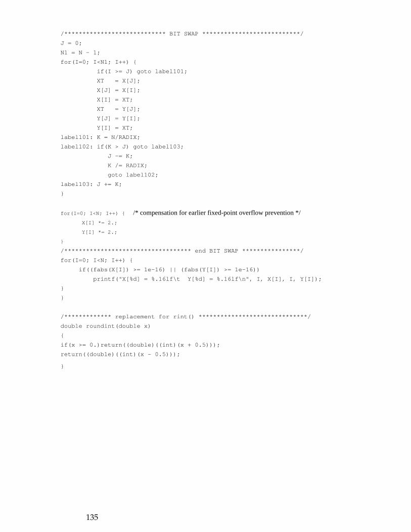
/**************************** BIT SWAP ***************************/
J = 0;
N1 = N - 1;
for(I=0; I<N1; I++)
if(I >= J) goto label101;
XT = X[J];
X[J] = X[I];
X[I] = XT;
XT = Y[J];
Y[J] = Y[I];
Y[I] = XT;
label101: K = N/RADIX;
label102: if(K > J) goto label103;
J -= K;
K /= RADIX;
goto label102;
label103: J += K;
for(I=0; I<N; I++) /* compensation for earlier fixed-point overflow prevention */
X[I] *= 2.;
Y[I] *= 2.;
/*********************************** end BIT SWAP ****************/
for(I=0; I<N; I++)
if((fabs(X[I]) >= 1e-16) || (fabs(Y[I]) >= 1e-16))
printf("X[%d] = %.16lf\t Y[%d] = %.16lf\n", I, X[I], I, Y[I]);
/************* replacement for rint() ******************************/
double roundint(double x)
if(x >= 0.)return((double)((int)(x + 0.5)));
return((double)((int)(x - 0.5)));
135
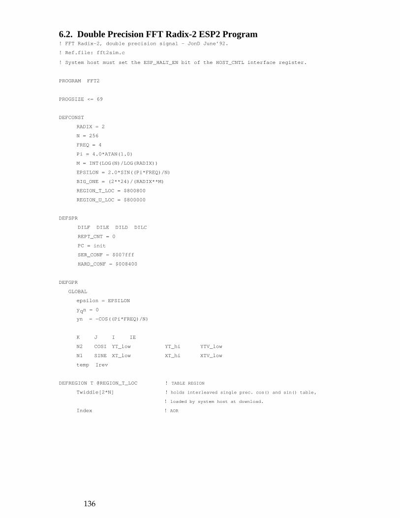
6.2. Double Precision FFT Radix-2 ESP2 Program! FFT Radix-2, double precision signal - JonD June’92.
! Ref.file: fft2sim.c
! System host must set the ESP_HALT_EN bit of the HOST_CNTL interface register.
PROGRAM FFT2
PROGSIZE <= 69
DEFCONST
RADIX = 2
N = 256
FREQ = 4
Pi = 4.0*ATAN(1.0)
M = INT(LOG(N)/LOG(RADIX))
EPSILON = 2.0*SIN((Pi*FREQ)/N)
BIG_ONE = (2**24)/(RADIX**M)
REGION_T_LOC = $800800
REGION_U_LOC = $800000
DEFSPR
DILF DILE DILD DILC
REPT_CNT = 0
PC = init
SER_CONF = $007fff
HARD_CONF = $008400
DEFGPR
GLOBAL
epsilon = EPSILON
yqn = 0
yn = -COS((Pi*FREQ)/N)
K J I IE
N2 COSI YT_low YT_hi YTV_low
N1 SINE XT_low XT_hi XTV_low
temp Irev
DEFREGION T @REGION_T_LOC ! TABLE REGION
Twiddle[2*N] ! holds interleaved single prec. cos() and sin() table,
! loaded by system host at download.
Index ! AOR
136

DEFREGION U @REGION_U_LOC ! DELAYLINE REGION
Xarray[2*N] ! real input double precision interleaved. 0 root required.
Yarray[2*N] ! imaginary input double precision interleaved.
Xpointer @$2fd ! AOR declarations
Ypointer @$2fc ! ditto
XIpointer XLpointer ! used in butterfly
YIpointer YLpointer ! ditto
Xrev_pointer
Yrev_pointer
!************************************************************************!
CODE
!******************** generate input signal ******************************!
init:
MOV &Yarray[0] > Ypointer MOV &Xarray[0] > Xpointer
NOP CLR K
signal_loop:
!*** initialize double precision input arrays ***
CLR *(Ypointer) HALVE yqn > *(Xpointer) !overflow prevention in first butterfly.
CLR *(Ypointer(+)) CLR *(Xpointer(+)) !low word!
!*** oscillator ***
MOV yqn > MACP MOV yn > MACP
MACP - epsilon X yn > yqn
MACP + epsilon X yqn > yn
!*** end oscillator ***
!*** go around loop simple way ***
NOP ADDV ONE,K
NOP CMP K,#N
ASH ONE <<1 > MACP JMP signal_loop, NEQ > CMR
ADD Ypointer,MACP > Ypointer ADDV #2,Xpointer
!*************** end input signal generation *****************************!
137
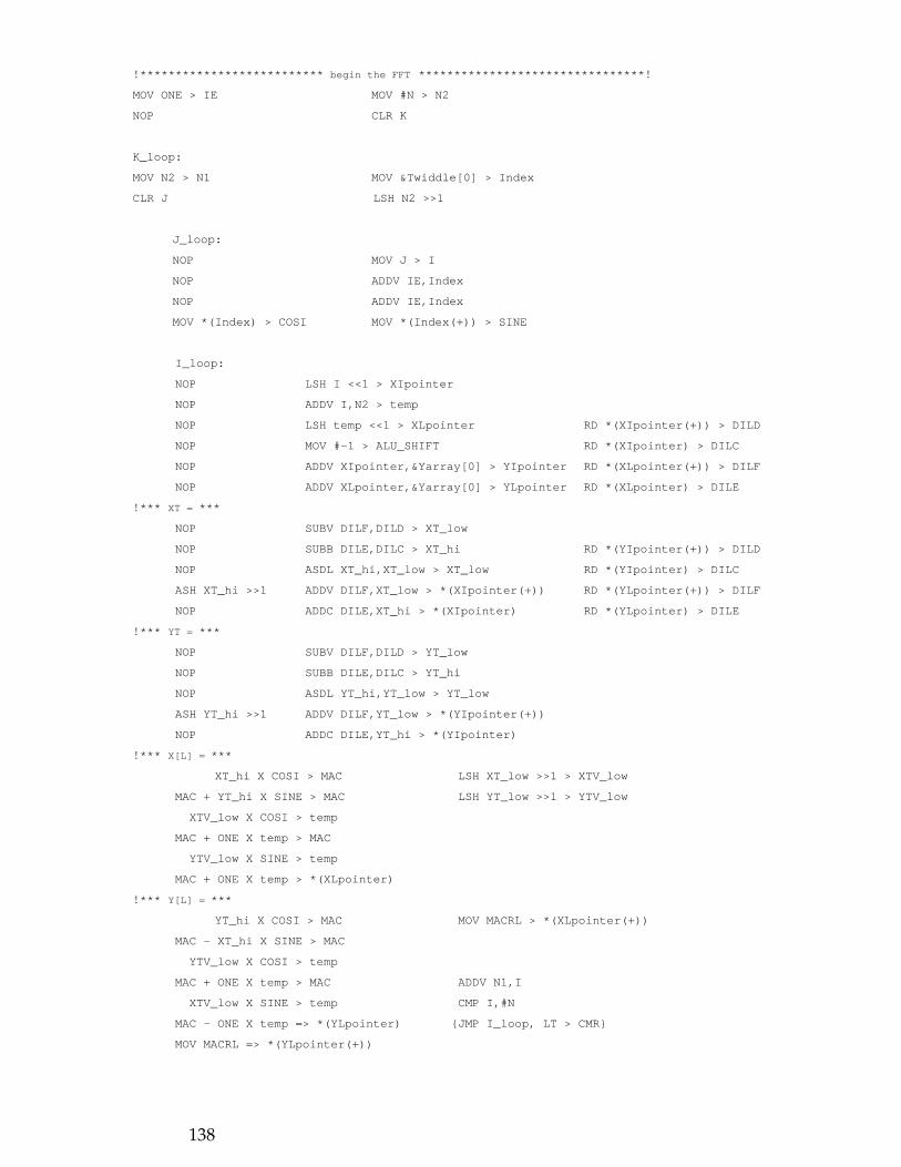
!************************** begin the FFT ********************************!
MOV ONE > IE MOV #N > N2
NOP CLR K
K_loop:
MOV N2 > N1 MOV &Twiddle[0] > Index
CLR J LSH N2 >>1
J_loop:
NOP MOV J > I
NOP ADDV IE,Index
NOP ADDV IE,Index
MOV *(Index) > COSI MOV *(Index(+)) > SINE
I_loop:
NOP LSH I <<1 > XIpointer
NOP ADDV I,N2 > temp
NOP LSH temp <<1 > XLpointer RD *(XIpointer(+)) > DILD
NOP MOV #-1 > ALU_SHIFT RD *(XIpointer) > DILC
NOP ADDV XIpointer,&Yarray[0] > YIpointer RD *(XLpointer(+)) > DILF
NOP ADDV XLpointer,&Yarray[0] > YLpointer RD *(XLpointer) > DILE
!*** XT = ***
NOP SUBV DILF,DILD > XT_low
NOP SUBB DILE,DILC > XT_hi RD *(YIpointer(+)) > DILD
NOP ASDL XT_hi,XT_low > XT_low RD *(YIpointer) > DILC
ASH XT_hi >>1 ADDV DILF,XT_low > *(XIpointer(+)) RD *(YLpointer(+)) > DILF
NOP ADDC DILE,XT_hi > *(XIpointer) RD *(YLpointer) > DILE
!*** YT = ***
NOP SUBV DILF,DILD > YT_low
NOP SUBB DILE,DILC > YT_hi
NOP ASDL YT_hi,YT_low > YT_low
ASH YT_hi >>1 ADDV DILF,YT_low > *(YIpointer(+))
NOP ADDC DILE,YT_hi > *(YIpointer)
!*** X[L] = ***
XT_hi X COSI > MAC LSH XT_low >>1 > XTV_low
MAC + YT_hi X SINE > MAC LSH YT_low >>1 > YTV_low
XTV_low X COSI > temp
MAC + ONE X temp > MAC
YTV_low X SINE > temp
MAC + ONE X temp > *(XLpointer)
!*** Y[L] = ***
YT_hi X COSI > MAC MOV MACRL > *(XLpointer(+))
MAC - XT_hi X SINE > MAC
YTV_low X COSI > temp
MAC + ONE X temp > MAC ADDV N1,I
XTV_low X SINE > temp CMP I,#N
MAC - ONE X temp => *(YLpointer) JMP I_loop, LT > CMR
MOV MACRL => *(YLpointer(+))
138
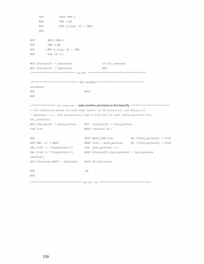
NOP ADDV ONE,J
NOP CMP J,N2
NOP JMP J_loop, LT > CMR
NOP
NOP ADDV ONE,K
NOP CMP K,#M
NOP JMP K_loop, LT > CMR
NOP LSH IE <<1
MOV &Xarray[0] > XIpointer JS bit_reversal
MOV &Yarray[0] > YIpointer NOP
!*************************** end FFT ************************************
!***************************** END PROGRAM ******************************
outahere:
NOP HALT
NOP
!*************** bit reversal / undo overflow prevention in first butterfly ************************
! This subroutine places the high order results in the Xarray[(+)] and Yarray[(+)]
! addresses; i.e., what we previously used to hold the low order double precision bits.
bit_reversal:
MOV &Xarray[0] > Xrev_pointer MOV &Yarray[0] > Yrev_pointer
CLR Irev REPT reversal,N-1
NOP ADDV #BIG_ONE,Irev RD *(Xrev_pointer) > DILF
ASH ONE <<1 > MACP BREV Irev > Xrev_pointer RD *(Yrev_pointer) > DILE
DBL DILF => *(XIpointer(+)) LSH Xrev_pointer <<1
DBL DILE => *(YIpointer(+)) ADDV &Yarray[0],Xrev_pointer > Yrev_pointer
reversal:
ADD YIpointer,MACP > YIpointer ADDV #2,XIpointer
NOP RS
NOP
!******************************* end bit rev ********************************
139

6.3. Double Precision FFT Radix-2 C-Program Simulation of ESP2 Program
/* reference file: fft2.c - JonD 6/15/92 */
/* This is a reduced precision (48-bit) rendering for ESP2 simulation.*/
/* Each stage of butterflys is scaled by 2 to prevent overflow. A sinusoid
will then have standard power level as output from scaled DFT (scaled by
factor N).
The complex input signal is stored in a double precision array for maximum
S/N through the FFT system. Multiplications with the input signal array
then, are in double precision.
*/
#include <stdio.h>
#include <math.h>
double pow2to46, select_lower24(), lower24();
double pow2to47, RoundInt48(), TruncInt48(), TruncInt48MAC();
double pow2to23, RoundInt24(), TruncInt24();
double pow2to15, TruncInt16(), RoundInt16(), roundint();
double myfmod();
#define NMAX 4096
#define FREQ 4 /* integer, empirical value. Period is always N/FREQ */
#define RADIX 2
#define TWIDDLE_SIZE 2*N
void main()
/* FFT */
char buf[32];
int N1, N2, M, IE, INDEX, I, J, K, L, N;
double COS, SIN, XT, YT;
double X[NMAX], Y[NMAX];
double noise_power;
/* TWIDDLE */
long templ;
double twopi, Wreal[NMAX], Wimag[NMAX];
/* INPUT SIGNAL */
double epsilon, yn, yqn;
double pi, amplitude, sinamp, sinamp_dB;
140
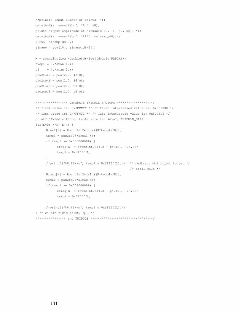
/*printf("Input number of points: ");
gets(buf); sscanf(buf, "%d", &N);
printf("Input amplitude of sinusoid (0. -> -90. dB): ");
gets(buf); sscanf(buf, "%lf", &sinamp_dB);*/
N=256; sinamp_dB=0.;
sinamp = pow(10., sinamp_dB/20.);
M = roundint(log((double)N)/log((double)RADIX));
twopi = 8.*atan(1.);
pi = 4.*atan(1.);
pow2to47 = pow(2.0, 47.0);
pow2to46 = pow(2.0, 46.0);
pow2to23 = pow(2.0, 23.0);
pow2to15 = pow(2.0, 15.0);
/**************** GENERATE TWIDDLE FACTORS *******************/
/* first value is: 0x7FFFFF */ /* first interleaved value is: 0x000000 */
/* last value is: 0x7FF622 */ /* last interleaved value is: 0xFCDBD5 */
printf("Twiddle factor table size is: %d\n", TWIDDLE_SIZE);
for(K=0; K<N; K++)
Wreal[K] = RoundInt24(cos((K*twopi)/N));
templ = pow2to23*Wreal[K];
if(templ >= 0x00800000L)
Wreal[K] = TruncInt24(1.0 - pow(2., -23.));
templ = 0x7fffffL;
/*printf("%0.6lx\n", templ & 0xffffffL);*/ /* redirect std output to get */
/* ascii file */
Wimag[K] = RoundInt24(sin((K*twopi)/N));
templ = pow2to23*Wimag[K];
if(templ >= 0x00800000L)
Wimag[K] = TruncInt24(1.0 - pow(2., -23.));
templ = 0x7fffffL;
/*printf("%0.6lx\n", templ & 0xffffffL);*/
/* 24-bit fixed-point, q23 */
/*************** end TWIDDLE *********************************/
141
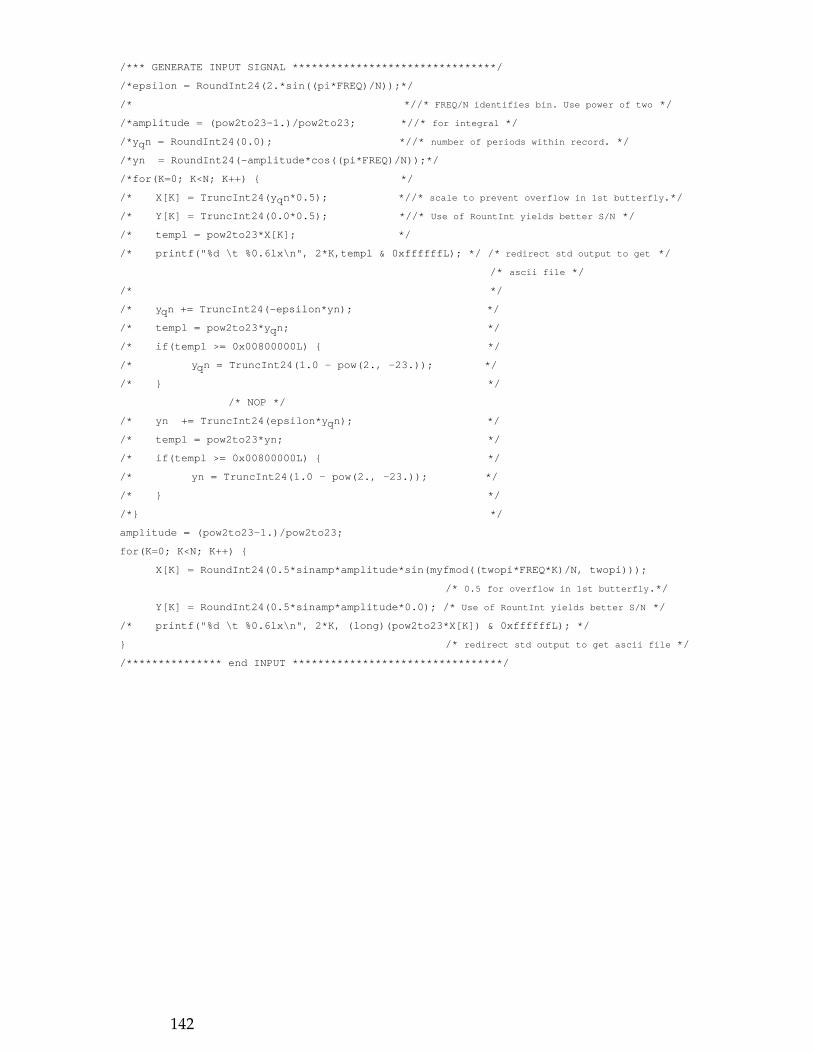
/*** GENERATE INPUT SIGNAL ********************************/
/*epsilon = RoundInt24(2.*sin((pi*FREQ)/N));*/
/* *//* FREQ/N identifies bin. Use power of two */
/*amplitude = (pow2to23-1.)/pow2to23; *//* for integral */
/*yqn = RoundInt24(0.0); *//* number of periods within record. */
/*yn = RoundInt24(-amplitude*cos((pi*FREQ)/N));*/
/*for(K=0; K<N; K++) */
/* X[K] = TruncInt24(yqn*0.5); *//* scale to prevent overflow in 1st butterfly.*/
/* Y[K] = TruncInt24(0.0*0.5); *//* Use of RountInt yields better S/N */
/* templ = pow2to23*X[K]; */
/* printf("%d \t %0.6lx\n", 2*K,templ & 0xffffffL); */ /* redirect std output to get */
/* ascii file */
/* */
/* yqn += TruncInt24(-epsilon*yn); */
/* templ = pow2to23*yqn; */
/* if(templ >= 0x00800000L) */
/* yqn = TruncInt24(1.0 - pow(2., -23.)); */
/* */
/* NOP */
/* yn += TruncInt24(epsilon*yqn); */
/* templ = pow2to23*yn; */
/* if(templ >= 0x00800000L) */
/* yn = TruncInt24(1.0 - pow(2., -23.)); */
/* */
/* */
amplitude = (pow2to23-1.)/pow2to23;
for(K=0; K<N; K++)
X[K] = RoundInt24(0.5*sinamp*amplitude*sin(myfmod((twopi*FREQ*K)/N, twopi)));
/* 0.5 for overflow in 1st butterfly.*/
Y[K] = RoundInt24(0.5*sinamp*amplitude*0.0); /* Use of RountInt yields better S/N */
/* printf("%d \t %0.6lx\n", 2*K, (long)(pow2to23*X[K]) & 0xffffffL); */
/* redirect std output to get ascii file */
/*************** end INPUT *********************************/
142
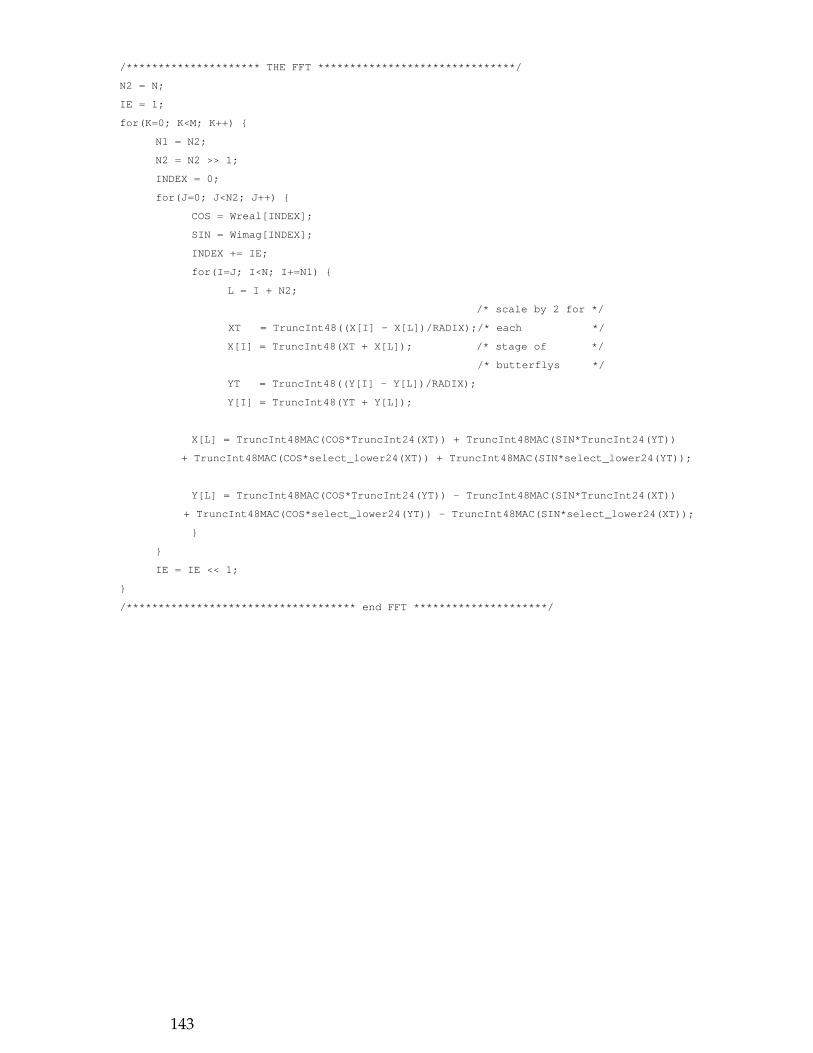
/********************* THE FFT *******************************/
N2 = N;
IE = 1;
for(K=0; K<M; K++)
N1 = N2;
N2 = N2 >> 1;
INDEX = 0;
for(J=0; J<N2; J++)
COS = Wreal[INDEX];
SIN = Wimag[INDEX];
INDEX += IE;
for(I=J; I<N; I+=N1)
L = I + N2;
/* scale by 2 for */
XT = TruncInt48((X[I] - X[L])/RADIX);/* each */
X[I] = TruncInt48(XT + X[L]); /* stage of */
/* butterflys */
YT = TruncInt48((Y[I] - Y[L])/RADIX);
Y[I] = TruncInt48(YT + Y[L]);
X[L] = TruncInt48MAC(COS*TruncInt24(XT)) + TruncInt48MAC(SIN*TruncInt24(YT))
+ TruncInt48MAC(COS*select_lower24(XT)) + TruncInt48MAC(SIN*select_lower24(YT));
Y[L] = TruncInt48MAC(COS*TruncInt24(YT)) - TruncInt48MAC(SIN*TruncInt24(XT))
+ TruncInt48MAC(COS*select_lower24(YT)) - TruncInt48MAC(SIN*select_lower24(XT));
IE = IE << 1;
/************************************ end FFT *********************/
143
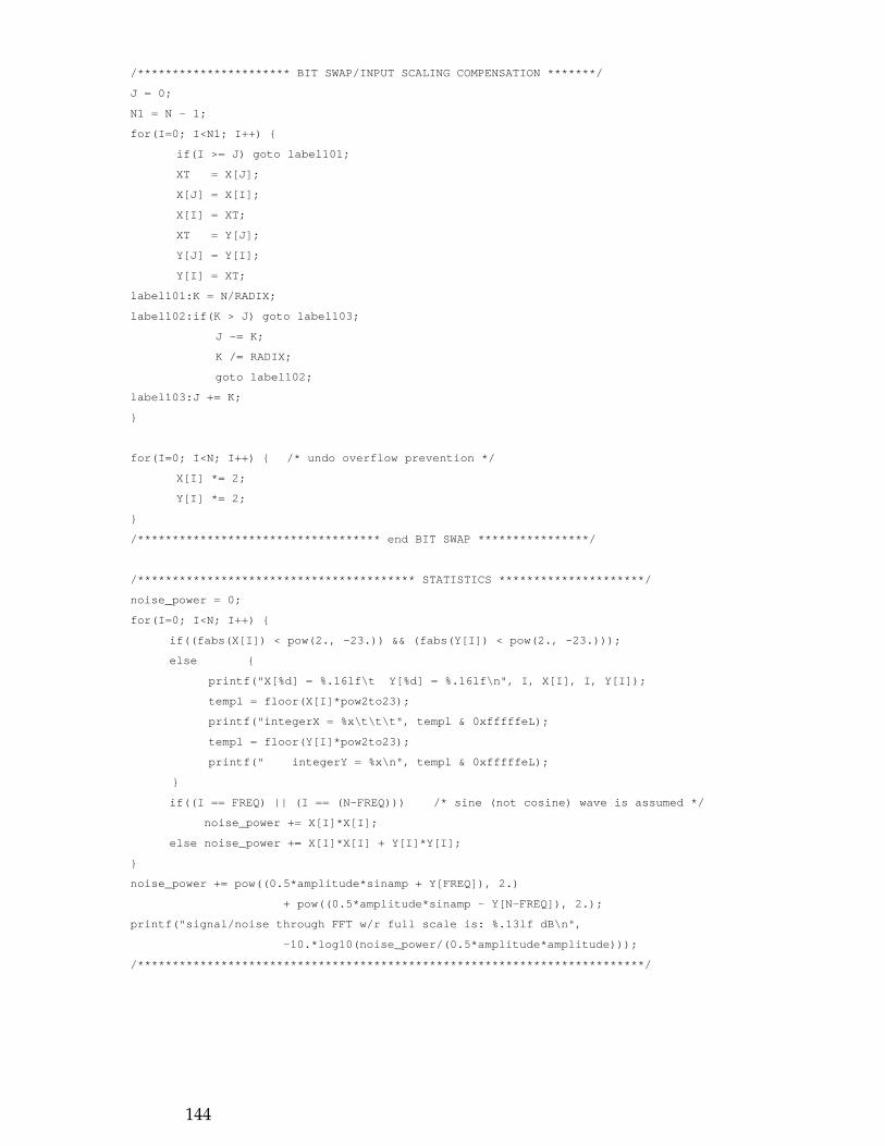
/********************** BIT SWAP/INPUT SCALING COMPENSATION *******/
J = 0;
N1 = N - 1;
for(I=0; I<N1; I++)
if(I >= J) goto label101;
XT = X[J];
X[J] = X[I];
X[I] = XT;
XT = Y[J];
Y[J] = Y[I];
Y[I] = XT;
label101:K = N/RADIX;
label102:if(K > J) goto label103;
J -= K;
K /= RADIX;
goto label102;
label103:J += K;
for(I=0; I<N; I++) /* undo overflow prevention */
X[I] *= 2;
Y[I] *= 2;
/*********************************** end BIT SWAP ****************/
/**************************************** STATISTICS *********************/
noise_power = 0;
for(I=0; I<N; I++)
if((fabs(X[I]) < pow(2., -23.)) && (fabs(Y[I]) < pow(2., -23.)));
else
printf("X[%d] = %.16lf\t Y[%d] = %.16lf\n", I, X[I], I, Y[I]);
templ = floor(X[I]*pow2to23);
printf("integerX = %x\t\t\t", templ & 0xfffffeL);
templ = floor(Y[I]*pow2to23);
printf(" integerY = %x\n", templ & 0xfffffeL);
if((I == FREQ) || (I == (N-FREQ))) /* sine (not cosine) wave is assumed */
noise_power += X[I]*X[I];
else noise_power += X[I]*X[I] + Y[I]*Y[I];
noise_power += pow((0.5*amplitude*sinamp + Y[FREQ]), 2.)
+ pow((0.5*amplitude*sinamp - Y[N-FREQ]), 2.);
printf("signal/noise through FFT w/r full scale is: %.13lf dB\n",
-10.*log10(noise_power/(0.5*amplitude*amplitude)));
/*************************************************************************/
144

/************************** print out ********************************/
/*for(I=0; I<N; I++)
templ = floor(X[I]*pow2to23);
printf("integerX[%d] = %x\t\t\t",2*I + 1, templ & 0xfffffeL);
templ = floor(Y[I]*pow2to23);
printf(" integerY[%d] = %x\n",2*I+514, templ & 0xfffffeL);
*/
/************************************************************************/
/****************************** SUBROUTINES *****************************/
double RoundInt48(x)
double x;
return(roundint(pow2to47*x)/pow2to47);
double RoundInt24(x)
double x;
return(roundint(pow2to23*x)/pow2to23);
double RoundInt16(x)
double x;
return(roundint(pow2to15*x)/pow2to15);
double TruncInt48(x)
double x;
return(floor(pow2to47*x)/pow2to47);
/******** replacement for rint() on NeXT O.S. v2.1 *******/
double roundint(double x)
if(x >= 0.)return((double)((int)(x + 0.5)));
return((double)((int)(x - 0.5)));
145

double TruncInt48MAC(x)
double x;
return(floor(pow2to46*x)/pow2to46);
double TruncInt24(x)
double x;
return(floor(pow2to23*x)/pow2to23);
double TruncInt16(x)
double x;
return(floor(pow2to15*x)/pow2to15);
double select_lower24(x) /* also loses the LSB; the 48th bit */
double x;
double TruncInt24(), tempd;
tempd = x - TruncInt24(x);
return(floor(pow2to46*tempd)/pow2to46);
double lower24(x)
double x;
double TruncInt24(), tempd;
tempd = x - TruncInt24(x);
return(floor(pow2to47*tempd));
/****************** MYFMOD function ********************************************/
/*** used to increase accuracy of sin routines ***/
/*** fmod() uses floor() instead of (int). ***/
/*** fmod() also failing to return values within |modulo| ***/
/*** Want (int), which is magnitude truncation, for negative arguments. ***/
double myfmod(argument, modulo)
register double argument, modulo;
return(argument - (int)(argument/modulo)*modulo);
/********************************* END subroutines *****************************/
146

6.4. Comments on the Double Precision FFT Radix-2 ProgramThe complex Twiddle factor table must be loaded into external memory before the ESP2program is run. The Twiddle factor table used here is the same as the one used before.To load external memory, another ESP2 Application must be run. See the ExternalMemory Host Access Application.
The other FFT ESP2 program was optimized for speed, whereas this FFT Radix-2 ESP2program is optimized for accuracy. This ESP2 program demonstrates the ability of ESP2to perform double precision multiplys, accumulations, and arithmetic. The complex inputsignal is generated at 24 bits, q23, but it is maintained at double precision (48 bits, q47)as it passes through the FFT stages. This shows that an unsigned multiplier is notnecessary for double precision math.109 Although the double precision results areavailable, the final output only extracts single precision results after the bit reversalsubroutine.
If we eliminate the rounding of the high precision input signal to 24-bits in the C-programsimulation, we will find the noise introduced by the FFT circuit itself. The simulationestimates the total noise power introduced by the FFT to be about 132 dB below unity;the noise power spectrum is well below that level. If we eliminate the rounding of thehigh precision Twiddle factors to 24-bits, the total noise power falls to about -242 dB.
6.5. Changes to ESP2 Program to make the IFFT (Radix-2)The same considerations apply as before.
I_loop:
NOP LSH I <<1 > XIpointer
NOP ADDV I,N2 > temp
NOP LSH temp <<1 > XLpointer RD *(XIpointer(+)) > DILD
NOP NOP RD *(XIpointer) > DILC
NOP ADDV XIpointer,&Yarray[0] > YIpointer RD *(XLpointer(+)) > DILF
NOP ADDV XLpointer,&Yarray[0] > YLpointer RD *(XLpointer) > DILE
!*** XT = ***
NOP SUBV DILF,DILD > XT_low
NOP SUBB DILE,DILC > XT_hi RD *(YIpointer(+)) > DILD
NOP ADDV DILF,DILD > *(XIpointer(+)) RD *(YIpointer) > DILC
NOP ADDC DILE,DILC > *(XIpointer) RD *(YLpointer(+)) > DILF
NOP NOP RD *(YLpointer) > DILE
!*** YT = ***
NOP SUBV DILF,DILD > YT_low
NOP SUBB DILE,DILC > YT_hi
NOP ADDV DILF,DILD > *(YIpointer(+))
NOP ADDC DILE,DILC > *(YIpointer)
109This fact was also demonstrated in [Dattorro] where double precision coefficients wereapplied to a recursive digital filter structure using the technique called residual coefficient coding.
147

7. Reverberation
note signnote sign
672 + EXCURSE
x
x
definition
23
24
Ζ-4217 x1. - damping
∑
xdamping
1800x
x
decay diffusion
31
33
142x
x
input diffusion 1
13
14
277x
x 21
22
107x
x 19
20
379x
x 15
16
Figure R. Simplified Small Plate-class Reverberation topology due toGriesinger. For the output tap structure (yL, yR) see the application program.Delayline taps at nodes 24 and 48 are modulating. JonD 1994
input diffusion 2
input diffusion 1 input diffusion 2
delayline, z-142
node name
∑∑
908 + EXCURSE
x
x
46
48
definition
Ζ-3163Ζ-3720
xdecay
2656x
x
decay diffusion
55
59
xdecay
Ζ-4453
3963
30 54
Ζ-0 -> -∞
predelay
∑xL
xR
x1/2
1. - damping
∑
xdamping
bandwidth∑
x1. - bandwidth
x
x x
decay
Ζ-1Ζ-1
Ζ-1
x
∑ ∑
∑ ∑
∑
∑ ∑
∑
∑
∑ ∑
∑
∑
∑
∑
∑
148
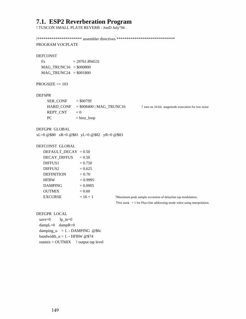
7.1. ESP2 Reverberation Program! TUSCON SMALL PLATE REVERB - JonD July’94 .
!********************** assembler directives *****************************
PROGRAM VOCPLATE
DEFCONST
Fs = 29761.894531
MAG_TRUNC16 = $000800
MAG_TRUNC24 = $001800
PROGSIZE <= 103
DEFSPR
SER_CONF = $007fff
HARD_CONF = $008400 | MAG_TRUNC16 ! turn on 16-bit magnitude truncation for low noise
REPT_CNT = 0
PC = bioz_loop
DEFGPR GLOBAL
xL=0 @$80 xR=0 @$81 yL=0 @$82 yR=0 @$83
DEFCONST GLOBAL
DEFAULT_DECAY = 0.50
DECAY_DIFFUS = 0.50
DIFFUS1 = 0.750
DIFFUS2 = 0.625
DEFINITION = 0.70
HFBW = 0.9995
DAMPING = 0.0005
OUTMIX = 0.60
EXCURSE = 16 + 1 !Maximum peak sample excursion of delayline tap modulation.
!Not used. + 1 for Plus-One addressing mode when using interpolation.
DEFGPR LOCAL
save=0 lp_in=0
dampL=0 dampR=0
damping_u = 1. - DAMPING @$6c
bandwidth_u = 1. - HFBW @$74
outmix = OUTMIX ! output tap level
149

DEFGPR GLOBAL /* The Knobs */
! input diffusion
diffus1 = DIFFUS1 @$75
diffus2 = DIFFUS2 @$77
! decay time
decay = DEFAULT_DECAY @$6e
! decay diffusion (decorrelates tank signals)
! Host computes: decay_diffus = decay + 0.15 q23, having: floor = 0.25, ceiling = 0.50
decay_diffus = DECAY_DIFFUS @$6f
! decay definition (controls density of tails)
definition = DEFINITION @$71
! High frequency damping
damping = DAMPING @$6d
! high frequency attenuation on input
bandwidth = HFBW @$73
DEFREGION V @$800000
node13_14[141]
node19_20[106]
node15_16[378]
node21_22[276]
node23_24[671+EXCURSE]
node24_30[4452]
node31_33[1799]
node33_39[3719]
node46_48[907+EXCURSE]
node48_54[4216]
node55_59[2655]
node59_63[3162]
predelay[42000] !optional
minus_one = SIZEM1V
GLOBAL
predelay_offset = &predelay[1] @$2de
!********************** end declarations *********************************
150

CODE
!******************************* ESP2 Code *****************************
!********* housekeeping ************
bioz_loop: NOP DIFF damping > damping_u
NOP DIFF bandwidth > bandwidth_u
!****************** a/d/a *************************************
ASH SER0L >>0 > xL !network has some gain! MOV yL > SER7L
ASH SER0R >>0 > xR MOV yR > SER7R
!************** load predelay ***************
NOP AVG xL, xR > predelay[0]
!************************ lowpass filter input ********************
bandwidth X *(predelay_offset) > MAC
MAC + bandwidth_u X lp_in > MAC, lp_in
!********** mono input 4 single stage guides ************************
NOP MOV node13_14[141] > MACP
MAC - diffus1 X "node13_14[141]" > node13_14[0]
MACP + diffus1 X "node13_14[0]" > MAC MOV node19_20[106] > MACP
MAC - diffus1 X "node19_20[106]" > node19_20[0]
MACP + diffus1 X "node19_20[0]" > MAC MOV node15_16[378] > MACP
MAC - diffus2 X "node15_16[378]" > node15_16[0]
MACP + diffus2 X "node15_16[0]" > MAC MOV node21_22[276] > MACP
MAC - diffus2 X "node21_22[276]" > node21_22[0]
MACP + diffus2 X "node21_22[0]" > MAC, save
!*************** decay ***************
MAC + decay X node59_63[3162] > MAC
!************** allpass 1 Left ******************************************
NOP MOV node23_24[671] > MACP
MAC + definition X "node23_24[671]" > node23_24[0]
MACP - definition X "node23_24[0]" > node24_30[0]
!************************** lowpass Left ***************************
damping_u X node24_30[4452] > MAC
MAC + damping X dampL > dampL
!*************** decay ***************
decay X dampL > MAC
151

!************************************ allpass 2 Left ***********************
NOP MOV node31_33[1799] > MACP
MAC - decay_diffus X "node31_33[1799]" > node31_33[0]
MACP + decay_diffus X "node31_33[0]" > node33_39[0]
!*************** decay ***************
MOV save > MACP
MACP + decay X node33_39[3719] > MAC
!************** allpass 1 Right ******************************************
NOP MOV node46_48[907] > MACP
MAC + definition X "node46_48[907]" > node46_48[0]
MACP - definition X "node46_48[0]" > node48_54[0]
!************************** lowpass Right ***************************
damping_u X node48_54[4216] > MAC
MAC + damping X dampR > dampR
!*************** decay ***************
decay X dampR > MAC
!************************************ allpass 2 Right ***********************
NOP MOV node55_59[2655] > MACP
MAC - decay_diffus X "node55_59[2655]" > node55_59[0]
MACP + decay_diffus X "node55_59[0]" > node59_63[0]
!***************************** Left Out *********************************
outmix X node48_54[266] > MAC
MAC + outmix X node48_54[2974] > MAC
MAC - outmix X node55_59[1913] > MAC
MAC + outmix X node59_63[1996] > MAC
MAC - outmix X node24_30[1990] > MAC
MAC - outmix X node31_33[187] > MAC
MAC - outmix X node33_39[1066] > yL !all wet
!**************************** Right Out *********************************
outmix X node24_30[353] > MAC
MAC + outmix X node24_30[3627] > MAC
MAC - outmix X node31_33[1228] > MAC
MAC + outmix X node33_39[2673] > MAC
MAC - outmix X node48_54[2111] > MAC
MAC - outmix X node55_59[335] > MAC
MAC - outmix X node59_63[121] > yR !all wet
!************************************ end Reverb *****************************!
NOP JMP bioz_loop
NOP BIOZ UPDATE BASEV += minus_one
!***************************************************************************!
152

7.2. Discussion of the Reverberation ProgramThe given ESP2 program is not the most efficient coding of the Reverb network possible.We have chosen to optimize the program for readability. The program as shown can becompressed by at least 12 instruction lines.
The Allpass Lattice TopologyThe eight lattices shown in the Reverb schematic are used in this effect as allpass filters,each having long impulse response time. The two coefficients within each individuallattice must remain identical to maintain the allpass transfer which is insensitive tocoefficient quantization. The recommended range of these coefficients is from 0.0 to0.9999999 (q23). Taking them both negative changes the character of the impulseresponse but does not destroy the allpass transfer. This change in character is exploited inthe lattices having the coefficients called definition in the schematic. If the latticecoefficients should exceed 1.0, instability will result.
Allpass response is the forced (steady state) response of the chosen lattice output.Because the impulse response of each individual lattice within the Reverb schematic is solong, in some cases the integration time constant of the human hearing system isexceeded. This means that the perception of the allpass filter output may be asdiscretized events; i.e., not allpass.
This allpass lattice topology tends to clip prematurely at internal nodes, so the input toeach lattice cannot be presented with full-scale signal at all frequencies. We like thisallpass lattice because it requires only two lines of ESP2 code to implement; observe thecoding of the four input diffusers.
Magnitude TruncationLattices produce distinct low-level tones, after input signal has been removed, known aszero-input limit cycles. The origin of these tones stems from ongoing signal quantization in arecursive topology. The spontaneous tones can be eliminated through the use of magnitudetruncation (truncation towards zero) of the double precision intermediate results written out tosingle or lower precision external memory. Magnitude truncation is well known to subduelimit cycles in digital networks composed of ladders and lattices.110 [Smith]
In this ESP2 program, magnitude truncation at the 16-bit level is activated in thedeclarations section since that is the presumed width of external memory. This meansthat every WR to external memory is automatically magnitude truncated to 16-bits.Alternatively, the magnitude truncation could be dynamically activated by the runningprogram itself so that only selected portions of the code utilize this feature. Only therecursive portions of the network require magnitude truncation; In Figure R, the WR tothe predelay does not require magnitude truncation.
110Magnitude truncation is never applied to data read from external memory in the ESP2.
153
The data is magnitude truncated only on its way out to external memory; i.e., the DOLSPRs are not permanently modified. This is advantageous when the 24-bit precisionDOL contents are reused as in the delayspec Quote Scheme. If external memory is 24bits in width (the maximum width supported by ESP2) then the need for magnitude truncation islessened. The ESP2 still provides for automatic magnitude truncation at the 24-bit level,however. Using a manual shifting scheme, magnitude truncation at other bit levels canalso be accommodated.
Magnitude truncation, in the specific case of Reverberator tank topologies employinglattice or ladder allpass networks, can reduce the circuit noise floor by 12 to 24 dB afterinput signal is removed. The reason that this is true is because the predominant noisemechanism is zero-input limit cycle oscillation,111 a multiplicity of which beingperceived as a whooshing, shushing noise floor. The magnitude truncation makes theReverb output eventually go to absolute zero, two’s complement. The disadvantage to itsuse is that the THD+N (Total Harmonic Distortion plus Noise) of a steady state sinusoidthrough the linear Reverb network can be increased by anywhere from 0 to 6 dB.
Delayline Tap ModulationIn the ESP2 program given, we do not show any delayline tap modulation. Linearinterpolation or, better yet, Allpass interpolation (as demonstrated in the Application of the same
name) can be efficiently employed to slowly modulate112 the nominal tap point of the twoindicated delaylines in the schematic. The modulation will introduce undulating pitchchange into the tank, the recirculating four lowest lattices in Figure R. As explained inthe Linear Interpolation Application, Linear interpolation will introduce time-varyinglowpass filtering as an artifact thus supplying some unaccounted damping. Allpassinterpolation overcomes this particular problem and is perfectly applicable to Reverbbecause the required pitch change is microtonal. The sinusoidal LFO driving themodulator is economical requiring only two lines of ESP2 code, while the LFO rate ofupdate is the same as the sample rate. For signals with much high frequency content,such as drums, these built-in modulators serve to break up some pretty audible modes.
There is no analogue to this modulation process in a real room (unless the walls aremoving). Without the modulation, we may well describe the imaginary space emulatedby the given digital circuit as being enclosed by a picket fence. The slow modulationserves to effectively increase the sheer number of resonances (eigentones, modes ofoscillation, picket density) in the tank. The number of resonances in a real room, hall, orplate is probably far beyond what is existent in our little (non-modulating) Reverbnetwork. In the case of drums, the modulation is a godsend. In the case of piano, themodulation, though slight, may be objectionable because of a perceived vibrato.
111Here we use the term ’limit cycle’ in the classical DSP sense.112at a rate on the order of 1 Hz, and at a peak excursion of about 8 samples for a sample rate ofabout 29.8 kHz,
154

Input DiffusersThe purpose of the four input diffusers is to quickly decorrelate the incoming signalbefore it reaches the tank. The tank recirculation can sometimes become perceptible ascyclic events if the input signal is not conditioned in this manner. This function becomesespecially important for the successful reverberation of percussive sounds.
No diffusion corresponds to zero-valued allpass coefficients, while coefficient magnitudesclose to unity produce buzzing local to the afflicted allpass. Optimal diffusion for the first-order allpass lies somewhere in a region closer to |0.5| than to the extreme values of thecoefficients. The preset values given in the declarations were arrived at by cut-and-try.113
FiltersThe three single pole direct form I lowpass filters, used for input signal bandwidthcontrol and Reverb tank damping, will not clip prematurely at any node [Dattorro,pg.857][Jackson,ch.11.3] as implemented. The bandwidth control tracks cutoff frequency,while the damping control is high when the damping filter cutoff frequency is low.
Each filter requires only two lines of ESP2 code. Because they are first-order lowpassfilters, any low-level zero-input limit cycles they might produce would be at DC; i.e.,they will not produce tones like the lattices. [Jackson,ch.11.5] Magnitude truncationcannot be engaged here because the 24-bit filter memory is internal. Any signaltruncation noise power spectrum generated by the filters themselves will be centered atDC, since it follows the pole frequency. The noise power spectrum peak gain is not greatbecause the one pole is typically relatively far from the unit circle.114
Output Tap PointsAs given in the ESP2 code, note that the tap structure forming the stereo output signal, yLand yR, is all wet (reverberated) signal. This particular tap structure is characteristic ofthe Plate-emulation class of Reverb networks.115 Also note that the output tap structureproduces a synthetic stereo image because the stereo input is converted to a monophonicsignal116 at the Reverberator input in this particular topology. Normally, the desiredoutput is a mix of the reverberated signal, yL and yR, with the original (dry, full bandwidth)stereo input signal, xL and xR. But we do not show a mixer in the a/d/a section of code.
113That Reverb is in commercial production.114Were the filters instead high-pass, limit cycle tones might be produced at Nyquist while thetruncation noise spectrum would also be concentrated there.115The physical ’Plate’, actually resident in some contemporary recording studios, fills a smallroom in some embodiments and is sometimes gold-plated. The input signal is typically injectedonto the plate via one or two transducers while each output is a sum of multifarious signal taps,each tap transduced at a different location on the plate.116The ALU’s AVG instruction is useful here.
155
Simple Reverb Networks117
We show, in Figure R, one particular network for producing reverberation. We believethat there must be a limitless variety of such networks. The question naturally arises as towhy the simple digital circuit shown produces a convincing reverberation. Consider theplucked string of the violin; its envelope may be described as having a coherentexponential decay. It is this character which is theorized to be one of the primarydiscriminants of non-reverberated sound. Reverberating this sound, on the other hand,would tend to randomize the string envelope and phase producing a bumpier, moredynamic decay.
Long before DSP chips could be integrated into sampler-type synthesizers, reverberatedsampled sound was simulated by altering the decay characteristics of recorded drysamples by randomizing an overlaid envelope applied at playback. While not absolutelyconvincing, it was enough to cause pioneers [Griesinger] [Blesser/Bader] to question thepremise of precipitative work [Schroeder] at Bell Labs during the early 60’s. One candeduce from that work that to achieve the ideal of colorless reverberation, the eigentonedensity needs to approach 3 per Hz. It can also be theorized that the limit on the numberof achievable eigentones is proportional to the total delayline memory. From our currentperspective we know that emulation of physical spaces can be convincingly performedusing signal processing bandwidths as low as 10-12 kHz. This is true because oftypically rapid acoustical absorption in the high frequency region, and because thedesired output is a mix. This bandwidth would then require about 30 thousandeigentones, hence about 64k of delayline memory. In the 1960’s, this amount was noteconomical.118
In Reverberator design, while a good general rule regarding delayline memory iscertainly ’the more the better’ [Griesinger], the efficient Reverb network shown herein119
stands as testimony that the eigentone density criterion, predicting about 88k memory, isnot a hard and fast rule. Of at least equal importance is the decorrelation of the decay.
117This discussion is adapted from [Blesser] and it is supplemented by Appendix III.118The Lexicon Model 224 Digital Reverberation System introduced in 1979, possessed only 16kwords of memory operating at a sample rate of 20 kHz. The Elecktromesstechnik, Wilhelm FranzK.G., EMT-250 Digital Reverberator distributed in the USA by Gotham Audio Corp. beginningin 1977, operated at a sample rate of 32 kHz having only 8k words of memory. The precursor tothis machine is described in [Oppenheim,ch.2].119given a 15 kHz processing bandwidth and having only 22k words of memory, not includingpredelay,
156

ColorOn the other hand, our Reverb network signal response is not colorless. Empirically wefind that some of the most sought commercial Reverbs are somewhat colored in theirfrequency responses. This means that they impose some audible resonances upon theinput signal. It is not unusual to find as many musicians and recording engineers wholike a particular Reverb as those who do not. We find that some recording engineers donot want accurate emulation of a physical space because the reflection density takes toolong to build; they, in fact, sometimes want instantaneous high density reflections withsmooth exponential decay of the envelope having randomization in only the phase trail.
Choosing a particular Reverb for a particular application is commonplace, and purveyorsof such equipment have been known to purchase an audio signal processing box just toacquire one particular algorithm.120 At some level, choice of Reverb becomes a matterof taste much like art. There is no one universal reverberation network that satisfieseveryone for each and every application; we speculate that there never will.
DesignA technical chronicle of developments in the art of Reverberator design can be found in[Gardner]. That treatise surveys the very latest techniques. Gardner provides atranslation (from the French language) of the vanguard, Jot.
120much like buying a Compact Disc because one likes the title track.
157

8. Musical FilteringSmith gives a good introduction to classical digital filter theory in [Strawn,ch.2],requiring only basic knowledge of math from the reader. Here we discuss filteringrequirements for musicians whose criteria are quite different from those of the electronicsengineer.
8.1. Filter (Q) SelectivityElectronics engineers are accustomed to think of digital filters analytically in terms ofpole/zero number and locus, cutoff frequency, passband ripple, transition band or slope,stopband attenuation, etc. Musicians and recording engineers are more comfortablethinking in terms of filter parameters: gain or cut, center frequency, and filter Q(selectivity) or bandwidth. Formally, filter Q is defined as the positive quantity:
Q = ωc / ∆ω = ωc / (ω2 - ω1) (qqq)
;i.e., the center frequency divided by the bandwidth. The bandwidth is determined fromthe definition of the cutoff frequencies (ω1 and ω2). Traditionally, cutoff frequencies
occur at an absolute half-power level. In the prototypical case of a steep unity-gain(0 dB) lowpass filter, we recall this level as corresponding to the frequency locationwhere the magnitude-square transfer reaches -3.01 dB (=10 log10(1/2)).
But shallow audio filters may not have a 3 dB transfer excursion, so we must refine thedefinition of cutoff frequency in terms of half-power excursion; not an absolute level.
0 0.5 1 1.5 2 2.5 3
0.2
0.4
0.6
0.8
1
|Hc(z)|2
ωc = 1
Figure Cut. Cut filter excursion approx. 1.7 dB.
ω
cut depth2 = 0.669421
1 - 0.669421
1 - 0.834711= 1/2
power excursion
(0 769836, 0 834711) (1.269836, 0.834711)
half-power excursion points
bandwidth
1.269836 - 0.769836
ωc = 2 = Q
Absolute
ω2ω1
158

Take for example the cut filter magnitude-square transfer function shown in Figure Cut.This example transfer has a Q of 2. We define the two musical cutoff frequencies ascorresponding to the level at which
( 1 - |Hc(ejω)|2 ) / ( 1 - |Hc(ejωc)|2 ) = 1/2 (NNN)
We must solve this equation for ω; there are two solutions, ω1 and ω2. Referencing
Figure Cut, this equation instructs us to measure the bandwidth half-way down the troughof the magnitude square transfer. This makes intuitive sense. We cannot use thetraditional definition of cutoff frequency for this example because the trough is not deep
enough. But note that when |Hc(ejωc) |2 = 0 (the notch filter), the solution to (NNN)
corresponds to the classical definition of cutoff frequency.
The situation is pretty much the same for the resonator. Whereas the cut filterasymptotes to unity at z = ±1, the resonator is loosely defined as a second-order peakedfilter having a peak gain normalized to unity at its center frequency. The resonator can beformulated such that its magnitude square transfer is an exact flip of the correspondingcut filter about the horizontal half-power excursion line; i.e., symmetrical with the cutfilter. (This is why many of the numbers are exactly the same in Figure Reso as they arein Figure Cut.) We shall see how shortly.
0 0.5 1 1.5 2 2.5 3
0.2
0.4
0.6
0.8
1
|Hbnorm(z)|2
ωc = 1
Figure Reso. Resonator excursion approx. 1.7 dB.
ω
skirt depth2 = 0.669421
power excursion
(1.269836, 0.834711)
half-power excursion points
bandwidth
(0.769836, 0.834711)
1.269836 - 0.769836
ωc= 2 = Q
1 - 0.669421
1 - 0.834711= 1/2Absolute
ω1 ω2
159

For the resonator (the normalized boost filter) we acquire the two musical cutofffrequencies, ω1 and ω2 , solving the slightly different equation:
( 1 - |Hbnorm(ejω)|2 ) / ( 1 - |Hbnorm
(±1)|2 ) = 1/2 (RRR)
As before, the bandwidth is measured half-way up the peak of the magnitude squaretransfer. Again we note that when |Hbnorm
(±1)|2 = 0 (the perfect resonator), the solution to
(RRR) corresponds to the classical definition of cutoff frequency.
Having gained an understanding of musical filter Q, we begin with two unique andmusically useful digital filter transfer functions which just happen to fit our definition offilter selectivity:
8.2. The Cut FilterWhen constructing a notch filter, we expect there to be an absolute zero of transmission ata chosen place in the frequency-domain transfer. If we use a filter that just has zeroes(i.e., no poles), we can indeed make a notch. The problem is that the rest of the transferfunction will not be very flat as we might like it to be. We might also like a surgicalnotch; one that has high selectivity. For example, here is the magnitude transfer of a
notch filter evaluated at z = ejω, zero-radius R = 1, and zero-angle θ = 1 radian:
|1 - 2 R cos(θ) z-1 + R2 z-2|
0.5 1 1.5 2 2.5 3
0.5
1
1.5
2
2.5
3
ωFigure BN. A poor notch filter.
This transfer in Figure BN would pretty much obliterate a musical signal; especiallynoting the gain at high frequencies. Also, when the notch is moved to a new fixedlocation, the rest of the transfer changes its shape in an undesirable way. Hence, thisparticular notch filter is not very useful.
160
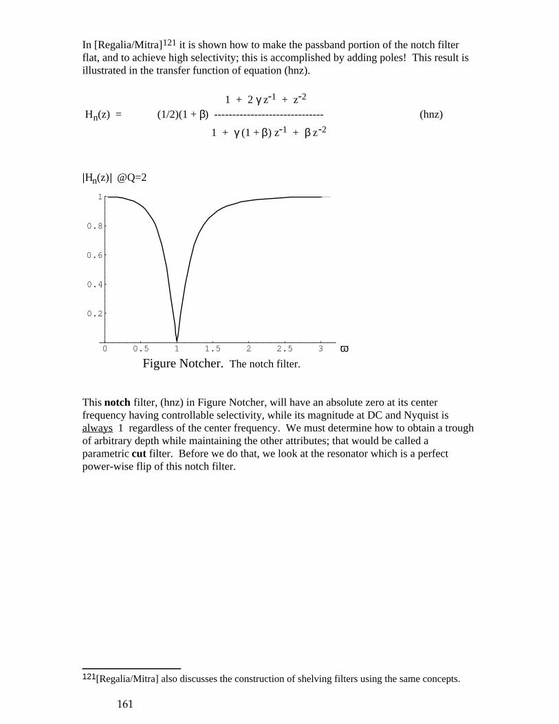
In [Regalia/Mitra]121 it is shown how to make the passband portion of the notch filterflat, and to achieve high selectivity; this is accomplished by adding poles! This result isillustrated in the transfer function of equation (hnz).
1 + 2 γ z-1 + z-2
Hn(z) = (1/2)(1 + β) ------------------------------ (hnz)
1 + γ (1 + β) z-1 + β z-2
|Hn(z)| @Q=2
0 0.5 1 1.5 2 2.5 3
0.2
0.4
0.6
0.8
1
ωFigure Notcher. The notch filter.
This notch filter, (hnz) in Figure Notcher, will have an absolute zero at its centerfrequency having controllable selectivity, while its magnitude at DC and Nyquist isalways 1 regardless of the center frequency. We must determine how to obtain a troughof arbitrary depth while maintaining the other attributes; that would be called aparametric cut filter. Before we do that, we look at the resonator which is a perfectpower-wise flip of this notch filter.
121[Regalia/Mitra] also discusses the construction of shelving filters using the same concepts.
161

8.3. The ResonatorWe discuss the use of a resonator as a filter. It is easy to construct a resonator using onlypoles. But such a transfer has problems similar to those we encountered with the all-zeronotch filter; particularly with the shape, selectivity, and magnitude evaluated along the
unit circle in the z-plane (i.e., at z = ejω). In particular, the peak magnitude will vary ascenter frequency is changed to new fixed values.
In [Jackson,ch.4.3] it is shown how to normalize the height of the resonator peak as thecenter frequency changes, by adding two zeroes; one at Nyquist and the other at DC!This musically useful result is distilled in equation (hrz).
1 - z-2
Hr(z) = (1/2)(1 - β) ---------------------------------- (hrz)
1 + γ (1 + β) z-1 + β z-2
|Hr(z)| @Q=2
0 0.5 1 1.5 2 2.5 3
0.2
0.4
0.6
0.8
1
ω Figure Peaker. The perfect resonator.
This filter has a peak gain which is always precisely 1, regardless of the center frequency.This is characteristic of a resonator. The two zeroes make the skirts of the magnituderesponse asymptote to zero at the extremities. When the extremities reach zero we callthis the perfect resonator, (hrz) shown in Figure Peaker. We must determine how tomake skirts of arbitrary depth; the resonator. We must also determine how to place theskirts at absolute magnitude 1 while achieving arbitrary peak heights; this would becalled a parametric boost filter.
162

8.4. Allpass Filter-TopologyThese two transfers, Hn(z) and Hr(z), have desirable theoretical and practical propertieswhich we will now expose. First, there is a strong bond between (hnz) and (hrz).Because their denominators are identical, there is one circuit that can generate both.
Consider the allpass lattice topology:
Figure Lattice. Lattice 2nd Order Allpass Filter
x
x
∑
∑-
β
Ζ-1x
x
∑
∑-
γ
Ζ-1
Dr(z)
Y(z)
X(z)
A(z)
The lattice in Figure Lattice has the allpass transfer function:
Y(z) β + γ (1 + β) z-1 + z-2
A(z) = ------ = -------------------------------- (ar0)
X(z) 1 + γ (1 + β) z-1 + β z-2
Some characteristics of the allpass are summarized:
|A(z)| = 1, A(±1) = 1, A(ejωc) = -1. (ar1)
-3 -2 -1 1 2 3
-6
-4
-2
2
4
6 A(ejω)
β = 0.86
Figure PhA.
ωc = 1
β = 0.36
ω
It is interesting that the allpass filter will shortly become integral to a parametric filterthat is a minimum phase design. We also note in passing that the transfer to Dr(z) fromthe input comprises only the denominator (the poles) of A(z):
X(z) Dr(z) = ---------------------------------
1 + γ (1 + β) z-1 + β z-2
163

Back to the problem at hand, it is easily proven that
Hr(z) = ( 1 - A(z) ) / 2 (hrz a)and
Hn(z) = ( 1 + A(z) ) / 2 (hnz a)
Substituting (ar0) into (hrz a) and (hnz a), we can respectively derive (hrz) and (hnz).This means that we can construct notch and perfect resonant filters from an allpass filter.We only have left to show that using the allpass we can construct cut, resonant, and boostfilters as well. We will use the fact (ar1) that at the critical frequency,
ωc = arccos(-γ) (wc1)
the allpass filter output is 180o out of phase with respect to a steady state sinusoid at its input.This critical frequency becomes the normalized center radian frequency ωc = 2π fc T (for T the
sample period) for all filter types employing the allpass filter-topology shown in Figure APDF1.
∑A(Ζ)
Figure APDF1. Cut, Notch, or Resonator Type Filter
x1/2
x1-k
x1 + |1-k|
2
We have introduced a new control coefficient, k. When k=0 this circuit inFigure APDF1 implements the notch (hnz a) exactly, and when k=2 this same circuitimplements the perfect resonator (hrz a) exactly. Within these bounds, this control (fork<1) gives us the ability to specify the depth of the cut, leaving the magnitude at theextremal frequencies equal to 1. Using the same circuit for the resonator, we can controlthe depth of the skirts (when k>1) leaving the absolute peak frequency magnitude atprecisely 1. These actions explain the unusual looking normalization at the output.
164

Table APDF1T k = 0 notch, Hn(z)
0 < k < 1 cut, Hc(z) k = 1 yields input signal
1 < k < 2 resonator, Hbnorm(z)
k = 2 perfect resonator, Hr(z)
0 0.5 1 1.5 2 2.5 3
0.2
0.4
0.6
0 8
1
|Hc(z)|2
ω
k=0k=2/5k=3/5k=4/5
Figure Cutter. Cut Transfer for various values of k, Q=2.
ωc = 1
The absolute cut depth = (1 - (1-k)) / (1 + |1-k|) = k / (2 - k) ;0 < k < 1 (cd1)
0 0.5 1 1.5 2 2.5 3
0.2
0.4
0 6
0.8
1|Hbnorm(z)|2
ω
k=2k=8/5k=7/5k=6/5
Figure Booster. Resonator Transfer for various values of k, Q=2.
ωc = 1
The absolute skirt depth = (1 + (1-k)) / (1 + |1-k|) = (2 - k) / k ;1 < k < 2 (sd1)
165
The cut and skirt depths must each be squared to resolve with Figure Cutter andFigure Booster. These depth equations are easily deduced from (wc1) and (ar1)respectively, and are independent of center frequency.
The center frequency is unequivocally determined by (wc1) for these cut, notch,resonator, and perfect resonator filters. This center frequency corresponds to the peak ortrough extremum of the magnitude transfer evaluated on the unit circle in the z-plane.
The ordinate axis is drawn at the lower half-power excursion frequency in the two graphsof Figure Booster and Figure Cutter. The half-power excursion frequencies (the twocutoff frequencies) are given for the cut, notch, resonator, and the perfect resonator by
(1+β)2 cos(ωc) +,- (β-1) √( 2(1+β2) - (1+β)2 cos2(ωc) )
cos(ω2,1) = ------------------------------------------------------------------- (w21)
2(1+β2)
1 - tan( ωc / (2 Q) )
β = ------------------------ (wbeta)1 + tan( ωc / (2 Q) )
Given a particular center frequency, the allpass lattice coefficient β precisely controlsselectivity (the filter Q) for these cut, notch, resonator, and perfect resonator filters.122
Whereas the lattice coefficient γ is a function only of ωc as we see from inspection of
(wc1), here we see that β is a function of both ωc and Q as per our new definition,
(RRR) and (NNN). On one hand, it is very good that we have discovered closed formmathematical relationships describing how to modify the two lattice coefficients tocontrol the musical filter parameters. But from a musical control standpoint, we wouldlike to have a way to decouple the filter coefficients so that only one of them controls thecenter frequency while the other controls only the selectivity parameter. (We almost havethat in γ .) Later on, we will see another circuit topology which nearly reaches that ideal.
122This equation for β is exact in terms of the selectivity definition herein.
166

Regalia k Coefficients
∑A(Ζ)
Figure APDF2. Cut, Notch, or Boost Type Filter
x1/2
x x1+k
1-k1+k
In [Regalia/Mitra] it was understood that a simple change of coefficient would result in adesign which substitutes the parametric boost filter for the resonator, hence incurring the lossof the perfect resonator. Employing the same allpass filter-topology as before, thecoefficients in Figure APDF2 are derived from those in Figure APDF1 via the substitution
(1-k) -> (1-k) / (1+k) (sub1)and via a scaling by the boost factor k on the output, but only when k>1.
Table APDF2T k = 0 notch, Hn(z)
0 < k < 1 yields cut, Hc(z)
k = 1 input signal 1 < k < ∞ boost, Hb(z)
0 0.5 1 1.5 2 2.5 3
0.25
0.5
0.75
1
1.25
1.5
1.75
2
|Hc(z)|2
|Hb(z)|2
ω
k=√4/5
k=√2/5k=√3/5
k=0
k=√6/5k=√7/5k=√8/5k √2
Figure Regal. Cut and Boost Transfers for various values of k. Q=2.
ωc = 1
Regalia absolute cut depth = k ;0 < k < 1 (cd2) Regalia absolute boost = k ;1 < k < ∞ (sd2)
167

The cut depth and boost must each be squared to resolve with Figure Regal. Theseresults can be derived by substituting (sub1) into (cd1) and (sd1). As before these resultsare independent of center frequency. The combined plot in Figure Regal highlights thesymmetry of the cut with the boost filters, hence the symmetry of Q. In general, thefilters of Figure APDF1 and Figure APDF2 are minimum phase.
From the allpass characteristics (ar1) it can also be deduced that, independent of centerfrequency:
Regalia absolute skirt depth of boost filter = 1 ;1 < k < ∞ (sd2a)
The ordinate axis is again drawn at the lower half-power excursion frequency (the lower
cutoff frequency) in Figure Regal. The two cutoff frequencies ω2,1 for the boost filter are
derived using a slightly different equation as compared with that for the resonator,(RRR), but it can be shown that the results are the same as before; i.e., (w21) remainsvalid under:
( |Hb(ejω)|2 - 1 ) / ( |Hb(ejωc)|2 - 1 ) = 1/2 (NBNB)
Equation (NBNB) does not reduce to the classical definition of cutoff frequency,
however, because Hb(ejωc) by definition is never zero. Because we were able to derivethe Regalia k coefficients (in Figure APDF2) from the circuit in Figure APDF1 whileretaining the same topology, all the equations thus far remain applicable; i.e., for β, γ,ωc , and ω2,1 .
Lattice Topology in PracticeThe foregoing allpass filter-topology constructed from the lattice suffers two drawbacksto its implementation: 1) The lattices produce spontaneous low-level audible zero-inputlimit cycle tones, 2) Lattice topologies are prone to signal overflow (hence conditionalsaturation in ESP2) at internal nodes before the allpass output has reached full scale.123
The first problem is solved by magnitude truncation of all lattice memory elements to 24bits. [Smith] Since the automatic magnitude truncation feature of the ESP2 can only beinvoked upon WR to external memory, it is clear that for these digital filters one does notwant to use internal memory; rather it is highly desirable to use 24-bit external memoryfor lattice memory storage.124
123In [Jackson,ch.4.3], a novel topology for the perfect resonator is shown.124If only 16-bit external memory is available, one is better off using 24 bit internal memory without
magnitude truncation.
168

The second problem (overflow) is solved by scaling the lattice input as already shown inFigure APDF1 and Figure APDF2. When premature internal overflow persists (which ismore likely for high Q, cut or boost), it becomes necessary to provide a user controlledinput-signal level adjustment.125 Compensation will be required at the filter output,under separate user-control. Keep in mind that the cost of any output compensation is theconcomitant amplification of the filter’s internal signal truncation noise floor, so thisinput scaling process should be limited.
As an alternative to the use of the allpass lattice, we recall that the direct form I filtertopology does not suffer from internal signal overflow because of its single accumulatorhaving infinite headroom. [Dattorro,pg.857&pg.875]126 [Jackson,ch.11.3] InFigure DirectLattice, we show an implementation of the second-order allpass filter (ar0)comprising embedded direct form I first-order allpass sections.127 This topology retainsthe dichotomy of the musical filter-coefficients as in the lattice, while employing thesame coefficients. Empirically, we observe that the limit cycle tones produced by thedirect form I are much quieter than those produced by the corresponding lattice inFigure Lattice, in general.128 Truncation error feedback (not shown) in the direct form isknown to further minimize limit cycle oscillation [Laakso], thus providing an alternativeto magnitude truncation as a remedy.
Figure DirectLattice. Direct Form I, 2nd Order Allpass Filter
β
γ
A(z)∑x
xΖ-1Ζ-1
Ζ-1Ζ-1
x
x ∑
−γ
−β
Ζ-1Ζ-1
x∑
x
γ
−γ
For both the lattice and embedded direct form, stability is assured by |γ|<1 and |β|<1.
125This knob is probably required anyway to compensate for filter boosts that the user requests. 126Overflow is not always a bad thing.127Conversion to direct form II using Rossum’s technique [RossumPat.] would eliminate some memory
elements while providing automatic input scaling. The scaling is necessary to prevent internal overflow in
that topology.128The direct form I may require error feedback [Dattorro] to be truncation noise competitivewith the lattice, however.
169

8.5. The Chamberlin Filter TopologyNow we consider high fidelity musical filtering using a different topology and themusician’s all-pole lowpass filter type. The musician’s all-pole filter has antecedents inthe electronic music industry appearing in currently renowned and vintage musicsynthesizers.129 [Curtis] The filters we previously considered had zeroes in the transfer.We were concerned about the control of those filters as a musician might like to controlthem. Here we present an additional goal; i.e., to come up with filter coefficients each ofwhich individually control only center frequency or selectivity (filter Q). To do so, were-derive the Chamberlin all-pole (two-pole) lowpass filter topology entirely from theperspective of the discrete-time domain.130
The electronics engineer’s lowpass has zeroes in the stopband and is very flat in thepassband.131 The stopband zeroes serve to provide high attenuation there. In contrast,musicians have a taste for peaked filters, even when the desired filter is of the lowpassvariety. Because the musician’s peak-center frequency is typically quite low (requiringpoles closer to the unit circle), zeroes are largely unnecessary due to the relatively highattenuation at frequencies far away from the poles. When the peak-center frequency ishigh, on the other hand, the excursion of the all-pole filter magnitude transfer may notreach 3 dB; in fact, when the peak-center frequency reaches π/2 the all-pole lowpassfilter ceases being lowpass because the magnitude transfer at π starts to exceed thetransfer at DC.
Due to the fact that the Chamberlin filter is all-pole, there is little control over the rate oftransition from pass to stop band. To increase the transition rate of the lowpass filter, theaccepted solution is to cascade an identical all-pole filter. This works in practice becausethe musician’s working range of the lowpass peak-center frequency is much less than π/2for reasonable sample rates. Zeroes placed at the Nyquist frequency, for example, wouldhave little impact over the musician’s working range. Therefore the cascade is preferredto zeroes at Nyquist. Zeroes elsewhere in the stopband region would entail morecomputation, hence they are undesirable. In this development, we will consider only asingle filter section.
129The classic Moog analog synthesizers, for example, employed fourth-order all-pole VoltageControlled Filters (VCF). His constant-Q design was also known as the Moog ladder , after theappearance of the schematic. The Chamberlin all-pole design is reputed resident within thecontemporary digital synthesizers by Peavey. A cascade of two Chamberlin filters can be consideredas the digital counterpart to the Moog VCF because many of the same characteristics are shared; theyare both all-pole constant-Q designs tuned by a single sweepable parameter.130This filter was originally derived from an analog State-Variable filter by application of theImpulse-Invariant transformation. [Chamberlin] points out that this circuit topologysimultaneously possesses a highpass and bandpass output at the nodes labelled hp and bp,respectively. We discuss only the lowpass filter function of this circuit in detail here.131The Butterworth filter for example (which is a good choice for audio with regard to minimalringing), has all its zeroes at Nyquist.
170
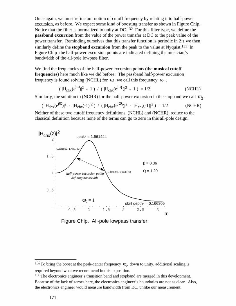
Once again, we must refine our notion of cutoff frequency by relating it to half-powerexcursion, as before. We expect some kind of boosting transfer as shown in Figure Chlp.Notice that the filter is normalized to unity at DC.132 For this filter type, we define thepassband excursion from the value of the power transfer at DC to the peak value of thepower transfer. Reminding ourselves that this transfer function is periodic in 2π, we thensimilarly define the stopband excursion from the peak to the value at Nyquist.133 InFigure Chlp the half-power excursion points are indicated defining the musician’sbandwidth of the all-pole lowpass filter.
We find the frequencies of the half-power excursion points (the musical cutofffrequencies) here much like we did before: The passband half-power excursionfrequency is found solving (NCHL) for ω; we call this frequency ω1 .
( |Hchx(ejω)|2 - 1 ) / ( |Hchx(ejωc)|2 - 1 ) = 1/2 (NCHL)
Similarly, the solution to (NCHR) for the half-power excursion in the stopband we call ω2 .
( |Hchx(ejω)|2 - |Hchx(-1)|2 ) / ( |Hchx(ejωc)|2 - |Hchx(-1)|2 ) = 1/2 (NCHR)
Neither of these two cutoff frequency definitions, (NCHL) and (NCHR), reduce to theclassical definition because none of the terms can go to zero in this all-pole design.
0.5 1 1.5 2 2.5 3
0.5
1
1.5
2
ω
|Hchx(z)|2
ωc = 1
β = 0.36
Figure Chlp. All-pole lowpass transfer.
peak2 = 1.961444
skirt depth2 = 0.166305
half-power excursion points defining bandwidth
(1.460898, 1.063875)
(0.631012, 1.480722)
Q = 1.20
132To bring the boost at the peak-center frequency ωc down to unity, additional scaling is
required beyond what we recommend in this exposition.133The electronics engineer’s transition band and stopband are merged in this development.Because of the lack of zeroes here, the electronics engineer’s boundaries are not as clear. Also,the electronics engineer would measure bandwidth from DC, unlike our measurement.
171

We begin with a simpler transfer function having no zeroes, so we can expect some of thepreviously discovered equations to be different.
αHchx(z) = ---------------------- (hchz)
1 + λ z-1 + β z-2
We seek the relationship of the coefficients to center frequency, ωc , and Q.
ωc = arccos( -(1 + β) λ / (4 β) ) (wcx)
If we express λ as λ = 4 β γ / (1 + β)
then we find the simpler expression for peak-center frequency.ωc = arccos( -γ ) (wc1)
This equation for center frequency is the same as before, and both (wc1) and (wcx) areexact.
At the peak-center frequency, the magnitude square transfer reaches its peak height;exactly:
4 α2 β
max( |Hchx(ejω)|2 ) = -------------------------
(β - 1)2 (4 β - λ2)
α2 (1 + β)2
= ---------------------------------------- (maxchx)(β - 1)2 ( 1 + β2 - 2 β cos(2 ωc) )
For the lowpass filter, we normalize the transfer to unity at DC, so α becomes:
α = 1 + λ + β
The two musical cutoff frequencies were determined exactly using Mathematica[Wolfram]134 as:
(cos,sin)2(ωc/2) (β-1) √(2(1+β2-2β cos(2 ωc)))
cos(ω2,1) = cos(ωc) +,- -----------------------------------------------------------------------------
√(1+β+8β2+β3+β4 - β(1-6β+β2) cos(2ωc) +,- 4β(1+β)2 cos(ωc))
(w21c)
134The extensions of Mathematica [Evans] to analog and digital signal processing are highlyrecommended.
172
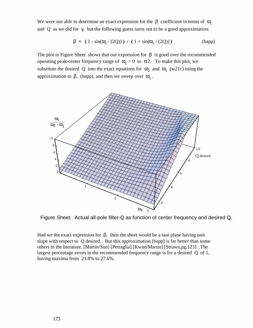
We were not able to determine an exact expression for the β coefficient in terms of ωc
and Q as we did for γ, but the following guess turns out to be a good approximation:
β ≈ ( 1 - sin(ωc / (2Q)) ) / ( 1 + sin(ωc / (2Q)) ) (bapp)
The plot in Figure Sheet shows that our expression for β is good over the recommendedoperating peak-center frequency range of ωc = 0 to π/2. To make this plot, we
substitute the desired Q into the exact equations for ω2 and ω1 (w21c) using the
approximation to β, (bapp), and then we sweep over ωc .
1
2
3
2
4
6
8
10
0
2
4
6
8
10
1
2
3
2
4
6
8
10
0
2
4
6
8
10
ωc
Q desired
ωcω2 - ω1
Figure Sheet. Actual all-pole filter-Q as function of center frequency and desired Q.
Had we the exact expression for β, then the sheet would be a taut plane having unitslope with respect to Q desired. But this approximation (bapp) is far better than someothers in the literature. [Martin/Sun] [Petraglia] [Kwan/Martin] [Strawn,pg.123] Thelargest percentage errors in the recommended frequency range is for a desired Q of 1,having maxima from 21.8% to 27.6%.
173

ApproximationsTo achieve our stated goal of obtaining filter coefficients which individually controlcenter frequency or filter selectivity, we now make series approximations to ourexpressions for the filter coefficients we have found thus far. The first several terms ofthe equivalent Maclaurin series for the z-1 coefficient in (hchz) are:
λ ≈ -(2 - ωc/Q - ωc2 + ωc
3 (1/(24 Q3) + 1/(2 Q)) + ωc4/12 + ...)
Using the good approximation (bapp) we find that the first several terms of the Maclaurinseries for the z-2 coefficient in (hchz) are:
β ≈ 1 - ωc/Q + ωc2/(2 Q2) - 5ωc
3/(24 Q3) + ωc4/(12 Q4) + ...
Figure CT shows the musical filter topology [Chamberlin]135 which implements atruncated series approximation to the desired filter coefficients, hence decouplingsomewhat the control of ωc and Q.
Hch(z)
Figure CT. Chamberlin Topology, All-Pole Filter.Trivial input/output compensation for internal overflow not shown.See Signal Overflow Analysis.
Fc
∑ Ζ-1
-
Ζ-1
∑ ∑
Qcx
x-
xhp bp
Fc
21
bpq
Y(z)X(z)
The all-pole lowpass transfer function of this further approximation to (hchz) in Figure CT is:
Y(z) Fc2 z-1
Hch(z) = ------ = --------------------------------------------------- ≈ z-1 Hchx(z) (hchs)
X(z) 1 - (2 - Fc Qc - Fc2) z-1 + (1 - Fc Qc) z-2
redefining: λ = -(2 - Fc Qc - Fc2) , β = 1 - Fc Qc , (hcsubs)
where, Fc ≈ 2 sin(ωc/2) radian, Qc ≈ 1/Q
The transmogrified numerator of (hchz) now shows a delay operator in (hchs). Thiscomes about because of the need to eliminate an otherwise delay-free loop in the circuitof Figure CT.136 The numerator coefficient α has become Fc
2 to force (hchs) to unity
at DC (z=1) as stipulated. This better approximation to Fc in (hcsubs) is from[Chamberlin] [Martin/Sun]. It becomes more exact for high Q where it is approximatelyωc when peak-center frequency is low. (An exact expression is given by (wcsx).)
135We adopt Chamberlin’s notation.136It is remarkable that the delay-free loop is eliminated without compromise to the digital filtercoefficients, because delay-free loops can be troublesome when it is desired to maintainautonomy of the analog coefficients in the transformation.
174
Stability/Parameter DecouplingStability of complex conjugate poles demands the constraint:
0 < (1 - Fc Qc) < 1
;restated: 0 < Fc < 1/Qc (stab0)
This condition is ascertained from (hchs) by demanding a pole radius137 of magnitudeless than one.
From previous considerations we presume that the tuning range for the all-pole lowpassfilter is: π/2 > ωc > 0. If we substitute (hcsubs) into the equation for actual peak-
center frequency ωc (wcx) in this range, we discover that Fc and Qc are not
completely decoupled138 except for very high selectivity (Qc ≈ 0):
4 (1 - Fc Qc) - Fc2 (2 - Qc
2) + Fc3 Qc
0 < cos(ωc) = --------------------------------------------- < 1 (wcsx)
4 (1 - Fc Qc)
We also find on the right-hand side that: Fc < 2/Qc - Qc
and on the left-hand side: Fc < ( -Qc + √(8 + Qc2) ) / 2
From the stability condition, (stab0), the minimum value of Fc is zero. This is achieved
for the right-hand side inequality above when Qc reaches √2. Thus we have an upperbound on Qc to keep the actual peak-center frequency within the prescribed tuningrange;
0 < Qc < √2.
To maintain complex conjugate poles in (hchs)139 we find that the following inequalityholds:
0 < (Fc + Qc) < 2
This is found by rooting the denominator of (hchs):
Fc2 z-1
Hch(z) = ---------------------------- (hchsroot)
(1 - a z-1) (1 - a* z-1)
where, a = 1 - Fc (Fc + Qc) / 2 + j Fc √(1 - (Fc + Qc)2/4)
Using the upper bound we found for Qc we see that there will always be some finite
range of Fc over which the poles will be complex conjugate.
137See (hrz) in Appendix V to see how to find the pole radius.138A similar conclusion can be reached by solving (bapp) for Q in terms of Fc and Qc via
(hcsubs). We leave this as an exercise. Note: (bapp) is an approximation while (wcsx) is exact.139i.e., for peak-center frequency away from but asymptotically including DC,
175

Combining all three criteria we finally conclude that to maintain a stable lowpass filter inthe form of (hchs) having complex conjugate poles conforming to the prescribed tuningrange, then the constraint must hold:
0 < Fc < min( 1/Qc , 2 - Qc , 2/Qc - Qc , (-Qc + √(8 + Qc2))/2 ) (stab1)
We learn from (stab1) that an artificial upper bound on the value of Qc equal to 1 yields
a universal upper bound on Fc equal to 1 as well (corresponding to ωc of about π/3).
We conclude that we can guarantee stability of complex conjugate poles for any value ofeither coefficient as long as they individually remain within the range 0 -> 1.
Peak GainWe examined the actual peak gain of Hch(ejω) over the prescribed ranges of Fc and Qc(both, 0 -> 1) substituting the truncated series approximation coefficients (hcsubs) into(maxchx) then taking the square root. We found the peak gain to be greater than but
approximately equal to Qc-1 . The largest excess beyond this estimate occurs for low
frequency and low Q, or for high frequency and high Q. At Fc = 0.000001 and Qc = 1
we found the greatest excess at about 15.5% over Qc-1 .
There is no separate control over peak gain in the Chamberlin topology; it is controlledindirectly through Qc . We recommend a maximum peak gain of 24 dB, for musicalpurposes, corresponding to a minimum Qc of about 0.0625 (filter Q=16).
176

8.5.1. Performance of the Chamberlin FilterNow we wish to know whether our approximations are good enough. To do this, anengineer might calculate the root locus of the Chamberlin poles to see how closely theirtrajectory matches that of a second-order constant-Q filter. Instead we will repeat themusical analysis, as in Figure Sheet, relating Q and center frequency; but this time wewill not use the ideal coefficients, rather we use the actual filter coefficients given by thetruncated series approximations in (hcsubs).
0.5
1
1.5
2
2
4
6
8
10
0
2
4
6
8
10
0.5
1
1.5
2
2
4
6
8
10
0
2
4
6
8
10
Fc
1/Qc
ωcω2 - ω1
Figure ChamSheet. Actual Chamberlin circuit Q as function of Fc and Qc-1 .
ωc , ω2 , and ω1 in Figure ChamSheet are calculated using the actual filter coefficients;
evaluating (wcsx) and by substituting (hcsubs) into (w21c). Figure ChamSheet tells thewhole story by relating actual circuit Q , (qqq), to the filter coefficients. Ideally, we arelooking for a planar relationship. Nonetheless, the sheet is fairly unwrinkled up to Fc ≈ 1,
corresponding to a tuning range of peak-center frequency up to π/3. Further, it appears thatfor our purposes the selectivity parameter control, Qc , is sufficiently decoupled from thetuning frequency control, Fc . Hence we can expect a good relationship of theory with
practice in that region.140
140At a sample rate of 44.1 kHz, π/3 corresponds to a bandwidth of 7350 Hz. Considering thatthe topmost note of the pianoforte reaches only 4186 Hz, that tuning range is good enough formusical purposes.
177

Integrator AnalysisGenerally speaking, it is not a good idea to implement an ideal digital integrator unless itcan be guaranteed that there exists a zero of transmission across it at DC. This iscertainly the case for integrator number 1 in Figure CT which has the required zeroacross it, but integrator number 2 has no such zero. In that case, one must then prove thatthere can exist no signal from any source having DC content upon arrival at the input tothe integrator under scrutiny. Audio signals normally enter the digital circuit at thedesignated input node, but noise having DC content is routinely generated in anypractical implementation at every node where signal truncation occurs. These noisesources most often appear in ESP2 at the input to each multiplier because multiplierinputs cannot accommodate double precision operands like the accumulators can.141 Thenoise is accurately modelled as a deterministic signal, input to a fictitious adder resting infront of the multiplier. Figure CTN demonstrates the application of the noise model toone of the noise sources (e2) on its way to integrator 2:
Figure CTN. Truncation Noise Source Model.
Ζ-1
∑xbp
e2[n]
2
Fc
∑I2
-Hch(z)
For the Chamberlin topology we have the remarkable result that the input to integratornumber 2 never sees any signal having DC content. For verification, we now look at themost interesting signal which is the noise source at the input to the multiplier at node bp.There we have,
I2(z) / e2(z) = -Fc (1 - (2 - Fc Qc) z-1 + (1 - Fc Qc) z-2) / ∆ (nn2)
where ∆ is the denominator of (hchs). The transfer (nn2) has a zero of transmission atDC which can be proven by substituting z=1. The three other possible signal sources (atnodes hp, bpq, and the input) acquire a simple zero of transfer at DC in the form, 1-z-1,by the time they arrive at I2.
141We presume no truncation post-accumulation for these integrators. This presumption isjustified based on the alternative which is a leaky integrator, requiring a multiply in its loop.
178
Truncation NoiseThe object of our noise analysis is to find the noise generated by the circuit itself whichthen appears at the observed output. The design goal of fidelity might be stated:
Criterion 1) It is desired that the filter circuit generate no noise which would fall abovethe spectral noise floor due to quantization of the original input signal.
Under this spectral interpretation of fidelity, the filter is then termed transparent to thesignal. This one is the more conservative of the two criteria for fidelity that we willconsider in this section.
Because the noise we are studying is deterministic (the sources are known), then when itoccurs early in a filter circuit topology it undergoes some filtering as does the input signalitself. Using the truncation noise model described for the integrator analysis, then, wewish to know the transfer from each of the noise sources to the lowpass output. Havingobtained this information, we can predict the frequency dependent amplification of eachpresumably wide-bandwidth noise source. Suppose, for example, that noise due totruncation were being generated at the 20-bit spectral level. Then any given noisetransfer would need to possess at least a 24 dB boost beyond unity (in any frequency region)before Criterion 1 were violated, assuming 16-bit signal fidelity.142
Like the one shown in Figure CTN, there are three noise sources arising due to thetruncation at each of the respective multiplier inputs; these are labelled hp, bpq, and bp inFigure CT:
1) The noise transfer from hp to the output is -Hch(z). This means that the noise transferfrom hp is the same as the signal transfer (with sign inversion), which is certainly not abad situation. This source is the largest of the noise contributors.
2) The noise transfer from bpq to the output is Qc Hch(z). We know that the peak gain
of Hch(z) is approximately Qc-1 , which means that the peak of this noise transfer from
bpq is about 1. This is good.
3) Lastly, we consider the noise transfer from bp to the output which can be written:1 - z-1
-------- Hch(z) - Qc Hch(z)
-Fc z-1
The first term introduces a zero at DC (but only to the noise), which is exactly what happenswhen we employ first-order truncation error feedback. [Dattorro] The zero squelches thenoise in the low frequency region but boosts it in the high frequency region. Using(hcsubs) we find that the crossover point (the point at which |1-z-1|/Fc=1), above which
the 1 - z-1 term begins to boost, is approximately ωc . In this particular circumstance,
142(20 - 16 bits) x 6 dB/bit = 24 dB. Another way of looking at this example would be to say thatunder fidelity Criterion 1, four extra bits would be required in the signal path to maintain filtertransparency if any one of the noise transfers were capable of a 24 dB gain in any frequencyregion; i.e., one bit for every 6 dB of gain beyond unity transfer. Refer to Appendix IV forsupporting noise concepts.
179

the second-order lowpass filter, Hch(z), kicks in above ωc to remove the boosted noise.
The second term of noise source 3 is like noise source 2 but opposite in polarity.143
Truncation Noise Power GainWhat we have thus far are the deterministic noise transfers which were of interest becauseof the way that the first criterion for fidelity was stated. The design goal of fidelity has asecond, quantitative (statistical) interpretation which is stated:
Criterion 2) It is desired that the total noise power generated by the filter circuit be lessthan the total noise power due to quantization of the original input signal.
This is the interpretation ubiquitously ascribed as the -6 dB total noise power perindividual bit. [Opp/Sch,pg.123] Here we determine the number of extra bits required tomaintain signal fidelity using this criterion. To do so we must calculate what iscommonly termed the noise gain. This is essentially an estimate of the total power boostof the internally generated, presumed spectrally white noise. Any total boost beyondunity is bad news, while any total gain of 1 or less is good.144 The calculation isperformed using the Parseval energy relation which integrates a noise transfer in eitherthe time or frequency domain. Hence the calculation result is unitless since the integrandis a ratio. From the noise transfers, we already know that the worst offender is the noisesource at hp. Substituting the poles of that transfer (hchsroot) into the integration resultsfrom [Opp/Sch,pg.187,357], we calculate the total noise power gain at hp as:
Fc4 (a(1 - a*2) - a*(1 - a2))
Nhp = -------------------------------------- (nstat)
(a - a*)(1 - a2)(1 - a*2)(1 - a*a)
143Unfortunately, they probably will not cancel each other due to the fact that the former mustpass through another truncation nonlinearity and a delay before it ever has the opportunity tocombine with this one. 144A total noise gain of 1 says that the noise transfer will not increase the total amount of noisethat it passes, but says nothing about the spectral distribution of the passed noise.
180

Qc
Nhp
00.2
0.40.6
0.81
0.20.4
0.60.8
1
0
2.5
5
7.5
10
00.2
0.40.6
0.81
0.20.4
0.60.8
1
0
2.5
5
7.5
10
Fc
Figure NPlot. Showing Nhp .
The vertical axis in Figure NPlot represents Nhp evaluated over the recommendedoperating ranges of Fc (0 -> 1) and Qc (1 -> 0.0625). We see that there is no totalnoise gain for Fc=0, because the filter is shut down at that point. But we also see that theworst total noise power boost occurs at hp for high center frequency and high Q whereNhp reaches 10.7826, which translates145 to 1.715 bits. The aggregate of the total noisepower contributions, generated by all the presumably uncorrelated noise sources in thecircuit of Figure CT, is calculated simply as Nhp + Nbpq + Nbp . This sum likelyrequires somewhat more than 2 extra bits (beyond the desired fidelity) in the signal path tomaintain fidelity using this latter criterion.
All in all, the all-pole lowpass Chamberlin topology looks good from the standpoint oftruncation noise performance. This is true because the pole gain, which is thedeterminant of noise gain in general, does not exceed the desired filter peak-gain for theChamberlin topology; the maximum pole gain is the maximum peak gain which werecommend to be 24 dB. The most significant improvement in noise performance wouldcome from further minimization of the hp noise source, like we saw in the case of the bpnoise source where truncation error feedback is built in.
14510 log(10.7826)/(20 log(2)) = log2(√10.7826) bits.
181

Limit Cycle OscillationZero-input limit cycling arises due to ongoing signal quantization within a recursivetopology; [Jackson] a nonlinear operation in an otherwise discrete linear system.146 Thefilter coefficients are parameters to limit cycles but are not the cause. Limit cyclesmanifest themselves as annoying low-level tones at a circuit’s outputs when no inputsignal is present. Signal quantization in ESP2 (as in most modern DSP chips) most often takesplace at the single precision multiplier inputs where double precision operands cannot beaccepted, so must be truncated.147 The limit cycle tones can therefore be visualized toenter the topology at the same places as the truncation noise. One such input port isshown in Figure CTN. Like the truncation noise sources, if limit cycle tones occur earlyin a filter topology they will be filtered like the signal (at the same point of entry) itself.
We now know that limit cycle oscillation is minimized by truncation error feedback[Laakso] which was devised to minimize the amplification of truncation noise. [Dattorro]Essentially, error feedback introduces zeroes into the noise transfer function, strategicallyplaced on the unit circle. A reasonable hypothesis is, therefore, that with or without errorfeedback, if the noise transfer from a quantizer to the output has a term 1-z-1 then itprovides some immunity to limit cycles as well as some squelching of truncation noise,both artifacts caused by that same quantizer.148 From our truncation noise analysis ofthe Chamberlin topology we see that only one of the truncation noise transfers has such aterm. Hence, limit cycle tones cannot be ruled out. Our only recourse is to minimizetheir amplitude of oscillation by providing internal signal truncation at lower levels. Thisis tantamount to providing higher precision signal paths.
Signal Overflow AnalysisThe study of overflow regards the observation of signal magnitude at sensitive nodes.Typically, one or several sensitive internal nodes may overflow (or underflow) sooner thanthe output. A saturation nonlinearity clips (appropriately full-scale positive or negative) theoverflowed node as this is highly preferable to a two’s complement wrap-aroundnonlinearity. The audible consequence of clipping at internal nodes is much moreobjectionable than clipping at the filter output, however, so it must be precludedcompletely. The sensitive internal nodes in ESP2 are, once again, the multiplier inputsbecause they cannot accept overflowed inputs like the accumulators can.149 These arelabelled hp and bp in Figure CT.
In our overflow analysis, what we are really interested in is the relationship of thesensitive nodes to the output. So we form a ratio, R, of transfers to the sensitive nodeswith respect to the transfer to the output node:
146Signal quantization converts a discrete-time system to a digital system.147Multipliers then produce double precision results which are usually fed to accumulators whichcan accept double precision inputs. 148In fact, [Laakso92] shows that any zero in the noise transfer provides some limit cycleimmunity. The common solution to both artifacts suggests that the two phenomena arehomologous.149Recall that most contemporary accumulators are designed to tolerate infinite intermediateoutput overflow simply by virtue of non-saturating adders. [Jackson,ch.11.3] So saturation at anaccumulator output (when necessary) is never performed upon intermediate accumulated results.
182

1) Node hp: Formulate Rhp(z) = ( hp(z)/X(z) ) / Hch(z) = (1-z-1)2 / (Fc2 z-1)
|Rhp(z)| = sin2(ω/2) / sin2(ωc/2)This describes a boost over the output at high frequencies. The worst case of overflowcomes at the highest frequency (z=-1) and for a peak-center frequency ωc at the top of its
recommended range (π/2), for there the boost over the unity output is by the factor 2.
2) Node bp: Formulate Rbp(z) = ( bp(z)/X(z) ) / Hch(z) = (1-z-1) / Fc
|Rbp(z)| = sin(ω/2) / sin(ωc/2)
Similarly, the worst case boost over the output is absolute √2.
Based on this analysis, a simple technique to eliminate internal signal overflow, which wehave found works quite well, is to precede the Chamberlin topology with a fixed inputlevel attenuation=1/2 and to follow with a compensation factor of 2 at the output. Theoutput compensation amplifies the filter’s internally generated truncation noise, however;i.e., the ratio of filtered signal power to the filter’s own total noise degrades by 6 dB.
As shown in Figure Chlp, the Chamberlin lowpass is a boosting filter. For some signalsthe output may overflow. But overflow at the output will not always occur because thefiltered signal may not have significant energy in the frequency region of the boost.Further, some small amount of output clipping is not offensive to the musician. Hence, it is not desirable to automatically normalize the filter peak gain for the musician byattenuating the input signal because there will be an objectionable loss in perceivedvolume. For then, the musician would demand a knob for output compensation; such aknob is emphatically discouraged because of the consequent amplification of internallygenerated truncation noise.
The most viable solution to the output overflow problem is to provide a filter inputsignal-level user control. The user then determines at what input level any clipping at theoutput becomes offensive. When an input level user control exists for a boosting filter, itbecomes unnecessary to provide user-controlled output compensation to maximize theoutput signal level.
183

Estimate of Coefficient WidthRegarding Fc , using (hcsubs), resolve 1 Hz in 50 at a sample rate, Fs=44100.
-log2( 2(sin(π 51/44100) - sin(π 50/44100)) ) ≈ 13 fractional bits.
In two’s complement Fc requires 14 bits, but Fc is never negative.
Qc minimum is 0.0625 for 24 dB maximum peak gain. This amount of gain requires atleast 4 fractional bits; 5 bits in two’s complement although Qc is always positive. Morebits are required for increased resolution of selectivity.
Estimate of Minimum Required Internal Signal Path Width (@24 dB maximum peak gain)
Bit Budget Attribute
N=16 output fidelity, assumed input signal quantization n= 2 truncation noise immunity (Criterion 2) o= 1 internal signal overflow prevention m= 1 6 dB limit cycle suppression+ r= max(0, (24/6)-n-m) signal path LSBs for user-controlled input level attenuation150
N+n+o+m+r = 21 bits total
This estimate maintains signal fidelity of N bits at the Chamberlin lowpass filter output.The filter internal signal path width can be minimized by reducing the maximum peakgain or by compromising the bit-fidelity requirement. It is interesting to note that underthe more conservative fidelity Criterion 1, the estimate of the required total number ofbits becomes 22; only one more bit (n=4, r=0). We see that the ESP2 single precisionpath width (24 bits) easily meets either fidelity requirement.
Assuming that the number of bits required to represent Qc is less than or equal to thenumber of bits representing Fc , then the integrating accumulators must retain at least
14 + 21 - 1 = 34 bits151 of precision under fidelity Criterion 2, and 35 bits of precision
under Criterion 1.
150Assuming that the filter internal signal path resolution exceeds the input signal resolution, thenno input signal information will be lost through the use of an input level control, provided that theattenuation is limited to the difference in resolution (6 dB per bit, 24 dB recommended). 151The subtraction of 1 is a consequence of the redundant sign bit in the product of a two’scomplement multiplication.
184
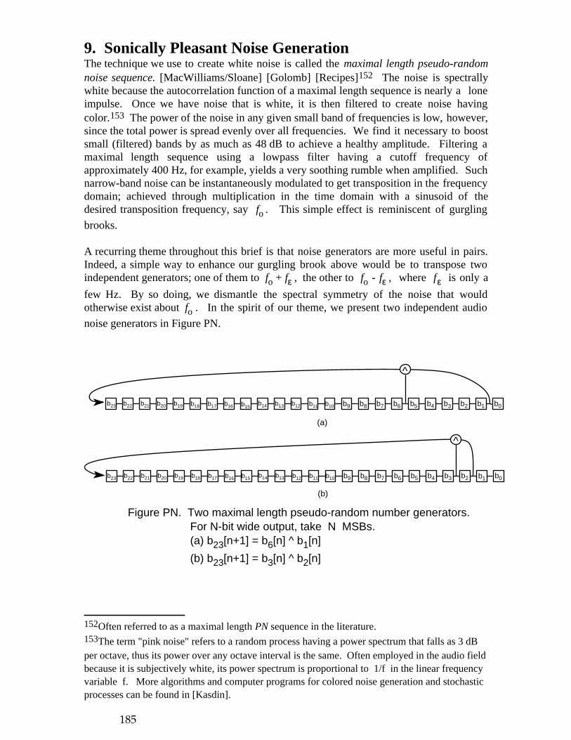
9. Sonically Pleasant Noise GenerationThe technique we use to create white noise is called the maximal length pseudo-randomnoise sequence. [MacWilliams/Sloane] [Golomb] [Recipes]152 The noise is spectrallywhite because the autocorrelation function of a maximal length sequence is nearly a loneimpulse. Once we have noise that is white, it is then filtered to create noise havingcolor.153 The power of the noise in any given small band of frequencies is low, however,since the total power is spread evenly over all frequencies. We find it necessary to boostsmall (filtered) bands by as much as 48 dB to achieve a healthy amplitude. Filtering amaximal length sequence using a lowpass filter having a cutoff frequency ofapproximately 400 Hz, for example, yields a very soothing rumble when amplified. Suchnarrow-band noise can be instantaneously modulated to get transposition in the frequencydomain; achieved through multiplication in the time domain with a sinusoid of thedesired transposition frequency, say fo . This simple effect is reminiscent of gurgling
brooks.
A recurring theme throughout this brief is that noise generators are more useful in pairs.Indeed, a simple way to enhance our gurgling brook above would be to transpose twoindependent generators; one of them to fo + fε , the other to fo - fε , where fε is only a
few Hz. By so doing, we dismantle the spectral symmetry of the noise that wouldotherwise exist about fo . In the spirit of our theme, we present two independent audio
noise generators in Figure PN.
Figure PN. Two maximal length pseudo-random number generators.For N-bit wide output, take N MSBs.(a) b23[n+1] = b6[n] ^ b1[n]
(b) b23[n+1] = b3[n] ^ b2[n]
b3b4b6b7b8b9b19b20b21b22b23 b11b12b13b14b15b16b17b18 b0b5
(b)
b1b10 b2
^
b23 b2b3b4b6b7b8b9b10b19b20b21b22 b11b12b13b14b15b16b17b18 b0b5
(a)
b1
^
152Often referred to as a maximal length PN sequence in the literature.153The term "pink noise" refers to a random process having a power spectrum that falls as 3 dBper octave, thus its power over any octave interval is the same. Often employed in the audio fieldbecause it is subjectively white, its power spectrum is proportional to 1/f in the linear frequencyvariable f. More algorithms and computer programs for colored noise generation and stochasticprocesses can be found in [Kasdin].
185
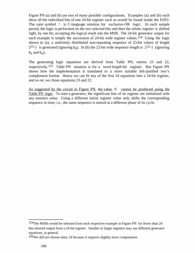
Figure PN (a) and (b) are two of many possible configurations. Examples (a) and (b) eachshow all the individual bits of one 24-bit register such as would be found inside the ESP2.The caret symbol ^ is C-language notation for exclusive-OR logic. At each sampleperiod, the logic is performed on the two selected bits and then the whole register is shiftedright, by one bit, accepting the logical result into the MSB. The 24-bit generator output foreach example is simply the succession of 24-bit wide register values.154 Using the logicshown in (a), a uniformly distributed non-repeating sequence of 23-bit values of length223-1 is generated (ignoring b0). In (b) the 22-bit wide sequence length is 222-1 (ignoringb1 and b0).
The generating logic equations are derived from Table PN; entries 23 and 22,respectively.155 Table PN notation is for a word length-bit register. But Figure PNshows how the implementation is translated to a more suitable left-justified two’scomplement format. Hence we can fit any of the first 24 equations into a 24-bit register,and so on; we chose equations 23 and 22.
As suggested by the circuit in Figure PN, the value 0 cannot be produced using theTable PN logic. To start a generator, the significant bits of its register are initialized withany nonzero value. Using a different initial register value only shifts the correspondingsequence in time; i.e., the same sequence is started at a different phase of its cycle.
154The MSBs would be selected from each respective example in Figure PN for fewer than 24bits-desired output from a 24-bit register. Smaller or larger registers may use different generatorequations, in general.155We did not choose entry 24 because it requires slightly more computation.
186

Table PN. Generating equations for maximal length sequences.156
word length generator word length generator 1 b0[n+1] = b0[n] 33 b32[n+1] = b13 ^ b0[n]
2 b1[n+1] = b1 ^ b0[n] 34 b33[n+1] = b15 ^ b14 ^ b1 ^ b0[n]
3 b2[n+1] = b1 ^ b0[n] 35 b34[n+1] = b2 ^ b0[n]
4 b3[n+1] = b1 ^ b0[n] 36 b35[n+1] = b11 ^ b0[n]
5 b4[n+1] = b2 ^ b0[n] 37 b36[n+1] = b12 ^ b10 ^ b2 ^ b0[n]
6 b5[n+1] = b1 ^ b0[n] 38 b37[n+1] = b6 ^ b5 ^ b1 ^ b0[n]
7 b6[n+1] = b1 ^ b0[n] 39 b38[n+1] = b4 ^ b0[n]
8 b7[n+1] = b6 ^ b5 ^ b1 ^ b0[n] 40 b39[n+1] = b21 ^ b19 ^ b2 ^ b0[n]
9 b8[n+1] = b4 ^ b0[n] 41 b40[n+1] = b3 ^ b0[n]
10 b9[n+1] = b3 ^ b0[n] 42 b41[n+1] = b5 ^ b4 ^ b3 ^ b2 ^ b1 ^ b0[n]
11 b10[n+1] = b2 ^ b0[n] 43 b42[n+1] = b6 ^ b4 ^ b3 ^ b0[n]
12 b11[n+1] = b7 ^ b4 ^ b3 ^ b0[n] 44 b43[n+1] = b6 ^ b5 ^ b2 ^ b0[n]
13 b12[n+1] = b4 ^ b3 ^ b1 ^ b0[n] 45 b44[n+1] = b4 ^ b3 ^ b1 ^ b0[n]
14 b13[n+1] = b12 ^ b11 ^ b1 ^ b0[n] 46 b45[n+1] = b8 ^ b5 ^ b3 ^ b2 ^ b1 ^ b0[n]
15 b14[n+1] = b1 ^ b0[n] 47 b46[n+1] = b5 ^ b0[n]
16 b15[n+1] = b5 ^ b3 ^ b2 ^ b0[n] 48 b47[n+1] = b7 ^ b5 ^ b4 ^ b2 ^ b1 ^ b0[n]
17 b16[n+1] = b3 ^ b0[n] 49 b48[n+1] = b6 ^ b5 ^ b4 ^ b0[n]
18 b17[n+1] = b7 ^ b0[n] 50 b49[n+1] = b4 ^ b3 ^ b2 ^ b0[n]
19 b18[n+1] = b6 ^ b5 ^ b1 ^ b0[n] 51 b50[n+1] = b6 ^ b3 ^ b1 ^ b0[n]
20 b19[n+1] = b3 ^ b0[n] 52 b51[n+1] = b3 ^ b0[n]
21 b20[n+1] = b2 ^ b0[n] 53 b52[n+1] = b6 ^ b2 ^ b1 ^ b0[n]
22 (b) b21[n+1] = b1 ^ b0[n] 54 b53[n+1] = b6 ^ b5 ^ b4 ^ b3 ^ b2 ^ b0[n]
23 (a) b22[n+1] = b5 ^ b0[n] 55 b54[n+1] = b6 ^ b2 ^ b1 ^ b0[n]
24 b23[n+1] = b4 ^ b3 ^ b1 ^ b0[n] 56 b55[n+1] = b7 ^ b4 ^ b2 ^ b0[n]
25 b24[n+1] = b3 ^ b0[n] 57 b56[n+1] = b5 ^ b3 ^ b2 ^ b0[n]
26 b25[n+1] = b8 ^ b7 ^ b1 ^ b0[n] 58 b57[n+1] = b6 ^ b5 ^ b1 ^ b0[n]
27 b26[n+1] = b8 ^ b7 ^ b1 ^ b0[n] 59 b58[n+1] = b6 ^ b5 ^ b4 ^ b3 ^ b1 ^ b0[n]
28 b27[n+1] = b3 ^ b0[n] 60 b59[n+1] = b1 ^ b0[n]
29 b28[n+1] = b2 ^ b0[n] 61 b60[n+1] = b5 ^ b2 ^ b1 ^ b0[n]
30 b29[n+1] = b16 ^ b15 ^ b1 ^ b0[n] 62 b61[n+1] = b6 ^ b5 ^ b3 ^ b0[n]
31 b30[n+1] = b3 ^ b0 [n] 63 b62[n+1] = b1 ^ b0[n]
32 b31[n+1] = b28 ^ b27 ^ b1 ^ b0[n] 64 b63[n+1] = b4 ^ b3 ^ b1 ^ b0[n]
156These logic equations are not unique, but all are suitable for audio. The time index, [n],appears once for each logic equation in this table because all time indices are the same on theright hand side. Note that bi[n] = bi-1[n+1] .
187
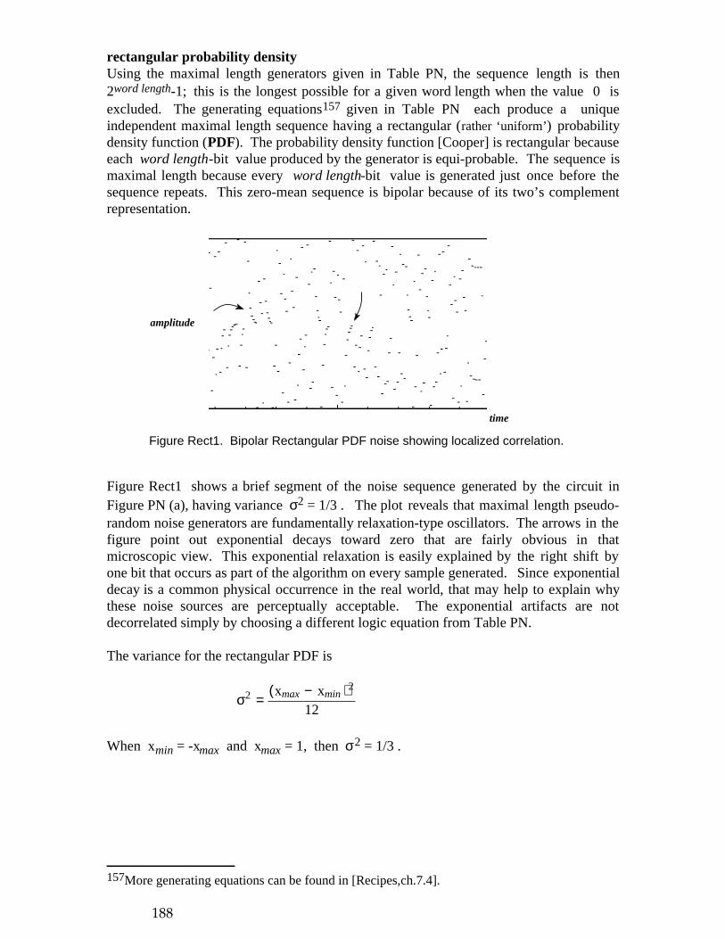
rectangular probability densityUsing the maximal length generators given in Table PN, the sequence length is then2word length-1; this is the longest possible for a given word length when the value 0 isexcluded. The generating equations157 given in Table PN each produce a uniqueindependent maximal length sequence having a rectangular (rather ‘uniform’) probabilitydensity function (PDF). The probability density function [Cooper] is rectangular becauseeach word length-bit value produced by the generator is equi-probable. The sequence ismaximal length because every word length-bit value is generated just once before thesequence repeats. This zero-mean sequence is bipolar because of its two’s complementrepresentation.
Figure Rect1. Bipolar Rectangular PDF noise showing localized correlation.
time
amplitude
Figure Rect1 shows a brief segment of the noise sequence generated by the circuit inFigure PN (a), having variance σ2 = 1/3 . The plot reveals that maximal length pseudo-random noise generators are fundamentally relaxation-type oscillators. The arrows in thefigure point out exponential decays toward zero that are fairly obvious in thatmicroscopic view. This exponential relaxation is easily explained by the right shift byone bit that occurs as part of the algorithm on every sample generated. Since exponentialdecay is a common physical occurrence in the real world, that may help to explain whythese noise sources are perceptually acceptable. The exponential artifacts are notdecorrelated simply by choosing a different logic equation from Table PN.
The variance for the rectangular PDF is
( )−=σ2
2
21xx nimxam
When xmin = -xmax and xmax = 1, then σ2 = 1/3 .
157More generating equations can be found in [Recipes,ch.7.4].
188
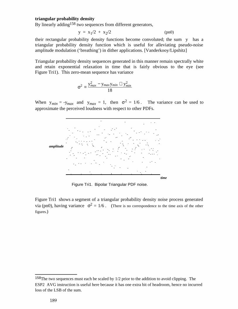
triangular probability densityBy linearly adding158 two sequences from different generators,
y = x1/2 + x2/2 (pn0)
their rectangular probability density functions become convoluted; the sum y has atriangular probability density function which is useful for alleviating pseudo-noiseamplitude modulation (‘breathing’) in dither applications. [Vanderkooy/Lipshitz]
Triangular probability density sequences generated in this manner remain spectrally whiteand retain exponential relaxation in time that is fairly obvious to the eye (seeFigure Tri1). This zero-mean sequence has variance
+−=σ
222
81yyyy nimnimxamxam
When ymin = -ymax and ymax = 1, then σ2 = 1/6 . The variance can be used toapproximate the perceived loudness with respect to other PDFs.
Figure Tri1. Bipolar Triangular PDF noise.
time
amplitude
Figure Tri1 shows a segment of a triangular probability density noise process generatedvia (pn0), having variance σ2 = 1/6 . (There is no correspondence to the time axis of the other
figures.)
158The two sequences must each be scaled by 1/2 prior to the addition to avoid clipping. TheESP2 AVG instruction is useful here because it has one extra bit of headroom, hence no incurredloss of the LSB of the sum.
189
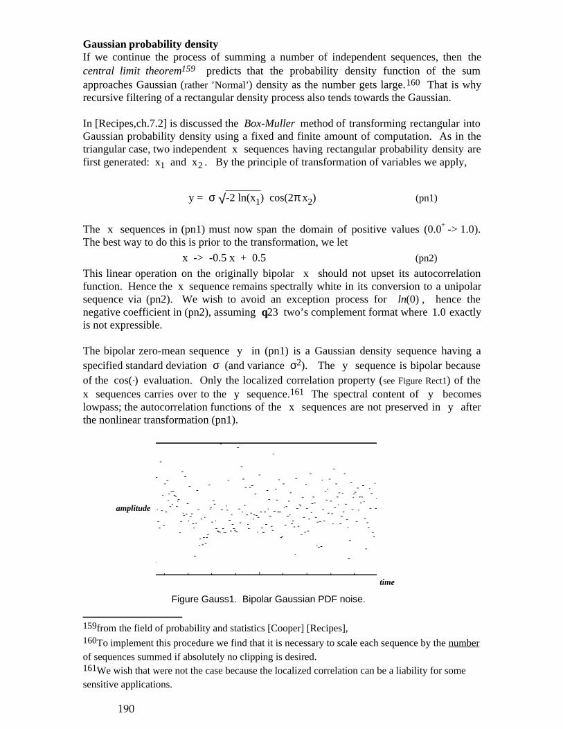
Gaussian probability densityIf we continue the process of summing a number of independent sequences, then thecentral limit theorem159 predicts that the probability density function of the sumapproaches Gaussian (rather ’Normal’) density as the number gets large.160 That is whyrecursive filtering of a rectangular density process also tends towards the Gaussian.
In [Recipes,ch.7.2] is discussed the Box-Muller method of transforming rectangular intoGaussian probability density using a fixed and finite amount of computation. As in thetriangular case, two independent x sequences having rectangular probability density arefirst generated: x1 and x2 . By the principle of transformation of variables we apply,
y = σ -2 ln(x1) cos(2π x2) (pn1)√
The x sequences in (pn1) must now span the domain of positive values (0.0+ -> 1.0).The best way to do this is prior to the transformation, we let
x -> -0.5 x + 0.5 (pn2)
This linear operation on the originally bipolar x should not upset its autocorrelationfunction. Hence the x sequence remains spectrally white in its conversion to a unipolarsequence via (pn2). We wish to avoid an exception process for ln(0) , hence thenegative coefficient in (pn2), assuming q23 two’s complement format where 1.0 exactlyis not expressible.
The bipolar zero-mean sequence y in (pn1) is a Gaussian density sequence having aspecified standard deviation σ (and variance σ2). The y sequence is bipolar becauseof the cos(.) evaluation. Only the localized correlation property (see Figure Rect1) of thex sequences carries over to the y sequence.161 The spectral content of y becomeslowpass; the autocorrelation functions of the x sequences are not preserved in y afterthe nonlinear transformation (pn1).
Figure Gauss1. Bipolar Gaussian PDF noise.
time
amplitude
159from the field of probability and statistics [Cooper] [Recipes], 160To implement this procedure we find that it is necessary to scale each sequence by the numberof sequences summed if absolutely no clipping is desired.161We wish that were not the case because the localized correlation can be a liability for somesensitive applications.
190

In [Recipes] it is explained that the sin(.) function can replace cos(.) in (pn1), and atechnique is shown to eliminate the trigonometric function evaluation altogether.162
Because ln(x1) can approach negative infinity, we must choose σ according to thedynamic range of the number system we are working within. But there will always beoutliers generated by (pn1). A remedy might be to allow some numerical wrapping of yin those events. The Gaussian probability density function will then become aliased163
and a tradeoff must be made between the aberration to the density function caused byclipping and that caused by wrapping.
Figure Gauss1 shows a brief segment from a Gaussian noise process having σ = 0.3generated via (pn1). Conditional saturation (clipping) was used to handle outliers.
Sonic MusingThe author presently owns about five electronic gadgets for sonic noise generation.These devices are analog and emit electronically amplified sound through a speaker,except for one which consists of an encased fan driven by an induction motor. The fan-type unit was first purchased from Marpac Corp., NC, in 1977. Their analog noisegenerators, which amplify and filter transistor noise, were found to be suitable substitutesfor the earlier electromechanical version. The noise generators are used when sleeping,concentrating, or to block out unwanted ambient disturbances.
Several years ago, the same company announced a new ‘improved’ digital sonic noisegenerator. Not only is the noise generation digital and algorithmic, but the front panel isnow computerized. After living with the unit for a while, the author concluded that thenoise was not pleasant, so back it went to the factory for repair. Discussion with theMarpac engineer revealed that the device was operating within normal parameters andwas not in need of repair. He confided that he too liked the analog units better. We nolonger use that digital device, however, because it sounds bad. Nonetheless, the Marpaccompany claims growing sales of the digital unit.
The author has put noise generation algorithms into production for commercial musicalproducts, and into the fitting system164 that supports a customized hearing aid. Whenevaluating various algorithms, we used our ears. Our purpose for transcribing theseevents is to convey the knowledge that digital methods for noise generation are notinherently bad, but some algorithms sound better than others. We know that whenproperly filtered, the fundamental algorithm presented herein sounds as good as anyanalog method of noise generation; that was our ultimate criterion for choosing it.
162The technique to eliminate the trigonometric function evaluation reverts the domain of the xsequences back to (-1.0 -> 1.0), but now entails a new exception process: It must detect when thesum of the squares of x1 and x2 is in excess of unity. In that case, the pair is discarded and a
new pair is generated. (This fact was first brought to the author’s attention by Paul Hargrove.)This decision process brings with it a variable execution time that may be undesirable in somecircumstances.163 much like the analog sinc() function becomes the aliased sinc() function (the Dirichlet kernel)in the discrete domain,164 Audio’D, Hearing Solutions, Paoli PA, USA
191
References[Adams] Robert Adams, Tom Kwan, ‘Theory and VLSI Architectures for AsynchronousSample-Rate Converters’, Journal of the Audio Engineering Society, vol.41, no.7/8,pg.539, 1993 July, AES, 60 East 42nd St., New York NY, 10165 USA
[AnalogDevices] ADSP-2100 Family - Applications Handbook, vol.1, 1989, AnalogDevices, Inc., DSP Division, One Technology Way, Norwood MA, 02062 USA
[Andreas] David C. Andreas, ‘VLSI Implementation of a One-Stage 64:1 FIRDecimator’, 89th Convention of the Audio Engineering Society, Los Angeles,Preprint 2976 (G-4), 1990 September 21-25, AES, 60 East 42nd St., New York NY,10165 USA
[Beigel] Michael L. Beigel, ‘A Digital "Phase Shifter" for Musical Applications, Usingthe Bell Labs (Alles-Fischer) Digital Filter Module’, Journal of the Audio EngineeringSociety, vol.27, no.9, pp.673-676, 1979 September, AES, 60 East 42nd St., New YorkNY, 10165 USA
[Blesser] Barry Blesser, personal communication.
[Blesser/Bader] Barry A. Blesser, Karl-Otto Bader, Electric Reverberation Apparatus,United States Patent No.4,181,820, January 1, 1980
[Burrus/Parks] C.S. Burrus, T.W. Parks, DFT/FFT and Convolution Algorithms, 1985, Wiley-Interscience Publication, John Wiley and Sons, New York NY, USA
[Chamberlin] Hal Chamberlin, Musical Applications of Microprocessors, 1980, Hayden Books, 4300 West 62nd St., Indianapolis IN, 46268 USA
[Cooper] George R. Cooper, Clare D. McGillem, Probabilistic Methods of Signal andSystem Analysis, second edition, 1986, Oxford University Press, 2001 Evans Rd., Cary NC, 27513 USA
[Crochiere/Rabiner] Ronald E. Crochiere, Lawrence R. Rabiner, Multirate Digital SignalProcessing, 1983, Prentice-Hall, Inc., Englewood Cliffs NJ, 07632 USA
[Curtis] CEM3328 Four Pole Low Pass VCF, 1983, Curtis Electromusic Specialties,110 Highland Ave., Los Gatos CA, 95030 USA
192

[Dattorro] Jon Dattorro, ‘The Implementation of Recursive Digital Filters for High-Fidelity Audio’, Journal of the Audio Engineering Society, vol.36, no.11, pp.851-878,1988 November, AES, 60 East 42nd St., New York NY, 10165 USA.---------, Corrections to above, Journal of the AES, vol.37, no.6, pg.486, 1989 June---------, Addendum to above, Journal of the AES, vol.38, no.3, pp.149-151, 1990 March
[Dattorro2400] Jon Dattorro, ‘Using Digital Signal Processor Chips in a Stereo AudioTime Compressor/Expander’, 83rd Convention of the Audio Engineering Society, New York, Preprint 2500 (M-6), 1987 October 16-19, AES, 60 East 42nd St., New York NY, 10165 USA
[Dattorro89] Jon Dattorro, ‘The Implementation of Digital Filters for High FidelityAudio, Part II - FIR’, Audio in Digital Times, The Proceedings of the Audio EngineeringSociety 7th International Conference, Toronto, pp.168-180, 1989 May 14-17, AES, 60 East 42nd St., New York NY, 10165 USA
[DattorroPat.] Jon C. Dattorro, Albert J. Charpentier, David C. Andreas, ‘DecimationFilter as for a Sigma-Delta Analog-to-Digital Converter’, United States PatentNo.5,027,306, June 25, 1991
[Evans] B. L. Evans, L. J. Karam, K. A. West, J. H. McClellan, ‘Learning Signals andSystems with Mathematica’, IEEE Transactions on Education, vol.36, no.1, pp.72-78,1993 February
[Fliege/Wintermantel] Norbert J. Fliege, Jorg Wintermantel, ‘Complex Digital Oscillatorsand FSK Modulators’, IEEE Transactions on Signal Processing, vol.40, no.2, pp.333-342, 1992 February
[Gardner], W. G. Gardner, ‘Reverberation Algorithms’, in Applications of SignalProcessing to Audio and Acoustics, M. Kahrs, K. Brandenburg, editors, 1996, Kluwer Academic Publishers, 101 Philip Dr., Assinippi Park, Norwell MA, 02061 USA
[Golomb] Solomon W. Golomb, editor, Digital Communications with SpaceApplications, 1964, Peninsula Publishing, Los Altos CA, 94022 USA
[Gordon/Smith] John W. Gordon, Julius Orion Smith, ‘A Sine Generation Algorithm forVLSI Applications’, Proceedings of the International Computer Music Conference, 1985,pp.165-168, ICMA, 2040 Polk St. #330, San Francisco CA, 94109 USA
193

[Gray] Robert M. Gray, Source Coding Theory, 1990, Kluwer Academic Publishers, 101 Philip Dr., Assinippi Park, Norwell MA, 02061 USA
[Griesinger] David Griesinger, ‘Practical Processors and Programs for DigitalReverberation’, Audio in Digital Times, The Proceedings of the Audio EngineeringSociety 7th International Conference, Toronto, pp.187-195, 1989 May 14-17, AES, 60 East 42nd St., New York NY, 10165 USA
[Haija/Ibrahim] A. I. Abu-el-Haija, M. M. Al-Ibrahim, ‘Improving Performance ofDigital Sinusoidal Oscillators by means of Error Feedback Circuits’, IEEE Transactionson Circuits and Systems, vol.CAS-33, no.4, pp.373-380, 1986 April
[Hamming] R. W. Hamming, Numerical Methods for Scientists and Engineers, second edition, 1973, Dover Publications, Inc., 31 East 2nd St., Mineola, NY 11501
[Harris] Fredric J. Harris, ‘On the Use of Windows for Harmonic Analysis with theDiscrete Fourier Transform’, Proceedings of the IEEE, vol.66, no.1, pp.51-84, 1978 January
[Hartmann] W. M. Hartmann, ‘Flanging and Phasers’, Journal of the Audio EngineeringSociety, vol.26, no.6, pp.439-443, 1978 June, AES, 60 East 42nd St., New York NY,10165 USA
[Jackson] Leland B. Jackson, Digital Filters and Signal Processing, third edition, 1996,Kluwer Academic Publishers, 101 Philip Dr., Assinippi Park, Norwell MA, 02061 USA
[Kasdin] N. Jeremy Kasdin, ‘Discrete Simulation of Colored Noise and StochasticProcesses and 1/fα Power Law Noise Generation’, Proceedings of the IEEE, vol.83, no.5, pp.800-827, 1995 May
[Kim/Sung] S. Kim, W. Sung, ‘A Floating-Point to Fixed-Point Assembly ProgramTranslator for the TMS 320C25’, IEEE Transactions on Circuits and Systems II, vol.41, no.11, pp.730-739, 1994 November
[Kwan/Martin] T. Kwan, K. Martin, ‘Adaptive Detection and Enhancement of MultipleSinusoids Using a Cascade IIR Filter’, IEEE Transactions on Circuits and Systems,vol.36, no.7, pp.937-947, 1989 July
194

[Laakso] Timo I. Laakso, Error Feedback for Reduction of Quantization Errors due toArithmetic Operations in Recursive Digital Filters, Thesis for the degree of Doctor ofTechnology, Report 9, Otaniemi 1991, Helsinki University of Technology, Laboratory ofSignal Processing and Computer Technology, Otakaari 5A, SF-02150 Espoo, Finland
[Laakso92] Timo I. Laakso, Paulo S. R. Diniz, Iiro Hartimo, Trajano C. Macedo, Jr.,‘Elimination of Zero-Input and Constant-Input Limit Cycles in Single-QuantizerRecursive Filter Structures’, IEEE Transactions on Circuits and Systems-II, vol.39, no.9,pp.638-646, 1992 September
[Laakso/Välimäki] Timo I. Laakso, Vesa Välimäki, Matti Karjalainen, Unto K. Laine, ‘Splitting the Unit Delay - Tools for fractional delay filter design’, IEEE Signal Processing Magazine, vol.13, no.1, pp.30-60, 1996 January
[Lee] Francis F. Lee, ‘Time Compression and Expansion of Speech by the SamplingMethod’, Journal of the Audio Engineering Society, vol.20, no.9, pp.738-742, 1972November, AES, 60 East 42nd St., New York NY, 10165 USA.---------, also in Speech Enhancement, Jae S. Lim, editor, pp.286-290, 1983, Prentice-Hall, Inc., Englewood Cliffs NJ, 07632 USA
[Luthra] A. Luthra, ‘Extension of Parseval’s Relation to Nonuniform Sampling’, IEEETransactions on Acoustics, Speech, and Signal Processing, vol.36, no.12, 1988 December
[MacWilliams/Sloane] F. Jessie MacWilliams, Neil J. A. Sloane, ‘Pseudo-RandomSequences and Arrays’, Proceedings of the IEEE, vol.64, no.12, pg.1715, 1976 December
[Martin/Sun] K. W. Martin, M. T. Sun, ‘Adaptive Filters Suitable for Real-Time SpectralAnalysis’, IEEE Transactions on Circuits and Systems, vol.CAS-33, no.2, pp.218-229,1986 February (Also published in IEEE Journal on Solid-State Circuits, vol.SC-21, no.1)
[Moore] F. Richard Moore, Elements of Computer Music, 1990, Prentice-Hall, Inc.,Englewood Cliffs NJ, 07632 USA
[Moorer] J. Andrew Moorer, personal communication. Also in [Strawn,pg.70].
195
[Oppenheim] Alan V. Oppenheim, editor, Applications of Digital Signal Processing,1978, Prentice-Hall, Inc., Englewood Cliffs NJ, 07632 USA
[Opp/Sch] Alan V. Oppenheim, Ronald W. Schafer, Discrete-Time Signal Processing,1989, Prentice-Hall, Inc., Englewood Cliffs NJ, 07632 USA
[Petraglia] M. R. Petraglia, S. K. Mitra, J. Szczupak, ‘Adaptive Sinusoid Detection UsingIIR Notch Filters and Multirate Techniques’, IEEE Transactions on Circuits andSystems II, vol.41, no.11, pp.709-717, 1994 November
[Ramstad] Tor A. Ramstad, ‘Digital Methods for Conversion Between ArbitrarySampling Frequencies’, IEEE Transactions on Acoustics, Speech, and Signal Processing,vol.ASSP-32, no.3, pp.577-591, 1984 June
[Recipes] William H. Press, Saul A. Teukolsky, William T. Vetterling, Brian P. Flannery,Numerical Recipes in C, second edition, 1992, Cambridge University Press, 40 West 20th St., New York NY, 10011 USA
[Regalia/Mitra] Phillip A. Regalia, Sanjit K. Mitra, ‘Tunable Digital Frequency ResponseEqualization Filters’, IEEE Transactions on Acoustics, Speech, and Signal Processing,vol.ASSP-35, no.1, pp.118-120, 1987 January
[Renfors/Saramäki] M. Renfors, T. Saramäki, ‘Recursive Nth-Band Digital Filters - Parts I and II’, IEEE Transactions on Circuits and Systems, vol.CAS-34, no.1, pp.24-51,1987 January
[Rossum] Dave Rossum, ‘An Analysis of Pitch Shifting Algorithms’, 87th Convention ofthe Audio Engineering Society, New York, Preprint 2843 (J-6), 1989 October 18-21,AES, 60 East 42nd St., New York NY, 10165 USA
[RossumPat.] David P. Rossum, Dynamic Digital IIR Audio Filter and Method WhichProvides Dynamic Digital Filtering for Audio Signals, United States PatentNo.5,170,369, December 8, 1992
[Schafer/Rabiner] Ronald W. Schafer, Lawrence R. Rabiner, ‘A Digital Signal ProcessingApproach to Interpolation’, Proceedings of the IEEE, vol.61, pp.692-702, 1973 June
196

[Schroeder] Manfred Schroeder, ‘Natural Sounding Artificial Reverberation’, Journal ofthe Audio Engineering Society, vol.10, no.3, 1962 July, AES, 60 East 42nd St., New York NY, 10165 USA
[Slater] Robert Slater, Portraits in Silicon, 1987, The MIT Press, Massachusetts Instituteof Technology, Cambridge MA, 02142 USA
[Smith] Julius Orion Smith, ‘Elimination of Limit Cycles and Overflow Oscillations inTime-Varying Lattice and Ladder Digital Filters’, Music Applications of DigitalWaveguides, Report No. STAN-M-39, 1987 May, Center for Computer Research inMusic and Acoustics (CCRMA), Dept. Music, Stanford University, Stanford CA, 94305 USA
[Smith/Cook] Julius Orion Smith, Perry R. Cook, ‘The Second-Order Digital WaveguideOscillator’, Proceedings of the International Computer Music Conference, 1992, pp.150-153, ICMA, 2040 Polk St. #330, San Francisco CA, 94109 USA
[SmithIII] Julius Orion Smith III, Techniques for Digital Filter Design and SystemIdentification with Application to the Violin, Report No. STAN-M-14, 1983 June, Center for Computer Research in Music and Acoustics (CCRMA), Dept. Music, Stanford University, Stanford CA, 94305 USA
[J.O.Smith] Julius O. Smith, An Allpass Approach to Digital Phasing and Flanging,Report No. STAN-M-21, Spring 1982, Center for Computer Research in Music andAcoustics (CCRMA), Dept. Music, Stanford University, Stanford CA, 94305 USA
[Smith/Friedlander] Julius O. Smith, Benjamin Friedlander, ‘Adaptive, InterpolatedTime-Delay Estimation’, IEEE Transactions on Aerospace and Electronic Systems,vol.21, no.2, pp.180-199, 1985 March
[Steiglitz] Ken Steiglitz, A Digital Signal Processing Primer, 1996, Addison-WesleyPublishing Company, 2725 Sand Hill Road, Menlo Park CA, 94025 USA
[Strawn] John Strawn, editor, Digital Audio Signal Processing, 1985, A-R Editions, Inc.,801 Deming Way, Madison Wisconsin, 53717 USA
[Thoen] Bradford K. Thoen, ‘Practical Aspects of Digital Sinewave Generation Using aSecond-Order Difference Equation’, IEEE Transactions on Circuits and Systems,vol.CAS-32, no.5, pp.510-511, 1985 May
197

[Vaidyanathan] P.P. Vaidyanathan, Multirate Systems and Filter Banks, 1993, Prentice-Hall, Inc., Englewood Cliffs NJ, 07632 USA
[Välimäki/Laakso] V. Välimäki, T. I. Laakso, J. Mackenzie, ‘Elimination of Transients inTime-Varying Allpass Fractional Delay Filters with Application to Digital WaveguideModeling’, Proceedings of the International Computer Music Conference, Banff, 1995, pp.327-334, ICMA, 2040 Polk St. #330, San Francisco CA, 94109 USA
[Vanderkooy/Lipshitz] John Vanderkooy, Stanley P. Lipshitz, ‘Digital Dither: SignalProcessing with Resolution Far Below the Least Significant Bit’, Audio in Digital Times,The Proceedings of the Audio Engineering Society 7th International Conference, Toronto,pp.87-96, 1989 May 14-17, AES, 60 East 42nd St., New York NY, 10165 USA
[Wolfram] Wolfram Research, Inc., Mathematica, Version 2, 1994, Champaign Illinois, 61820 USA
198

AcknowledgementsThe ESP2 chip was designed over a four year period beginning in 1990. The threeprincipal designers were David Andreas, Jon Dattorro, and J. William Mauchly (son ofJohn V. Mauchly, inventor of the ENIAC computer [Slater]). Andreas is the principalarchitect of the circuitry. He made the early computer models so as to simulate the chipprior to fabrication, and he provided the original Hardware Specification. Later in thedevelopment, David Dura planned the layout and implemented the chip in its entiretyemploying custom VLSI. Dura dedicated himself to chip debug and revision. MichaelArnao wrote the assembler. The ESP2 rests on the shoulders of its predecessor, the ESPchip. Although the two chips are divergent, the essence of that first design is retained. Inthis light, the pioneering work of Stephen Hoge and David DiOrio is recognized.
199

Appendix IESP2 Scheduler Notes: Rules for DIL and DOL Availability
We list the rules for DIL and DOL availability in scheduling external-memory accesses:
Glossary
AGEN read: an AGEN operation that reads the contents of an external-memory location into a DIL
AGEN write: an AGEN operation that writes the contents of a DOL to an external-memory location
defensive criterion: a criterion for determining DIL or DOL availability that tests whether the external-memory access currently being scheduled would be corrupted by a previously-scheduled access
initial operand: the topmost unquoted operand (A, B, C, D, E, F, or G) in a quoted-reference chain; this operand initializes the chain
isolated reference: an external-memory reference that is not the initial operand in a quoted-reference chain
latency: the difference between the number of the instruction where a register (GPR, AOR, or SPR) is written by a function unit (MAC, ALU, or AGEN) and the number of the instruction where the contents of that register become available as a source operand in a particular function unit
protective criterion: a criterion for determining DIL or DOL availability that tests whether a previously-scheduled external-memory access would be corrupted by the access currently being scheduled
quoted-reference chain: one or more quoted similar external-memory references preceded by an unquoted similar external-memory reference
request instruction: an instruction where an external-memory reference appears in the MAC unit or ALU as a source or destination operand
similar external-memory references: two or more external-memory references that refer to the same element of the same external-memory array in the same region and that have the same UPDATE BASE mode and same Plus-One addressing mode
200

target instruction: an instruction where an AGEN operation is to be coded by the assembler in response to an external-memory request from the MAC unit or ALU
terminal operand: the bottommost operand (A, B, D, or E) in a quoted-reference chain
Variables
’A_TO_B = k’ means that the latency from unit A to unit B is k instructions:
MAC_TO_MAC = 1MAC_TO_ALU = 1MAC_TO_AGEN = 0
ALU_TO_MAC = 2ALU_TO_ALU = 1ALU_TO_AGEN = 1
AGEN_TO_MAC = 2
AGEN_TO_ALU = 2
’A_PREC_B = k’ means that if a DOL is written by unit B at instruction n, and is subsequently written by unit A at instruction n+k, then at instruction (n+k+A_TO_AGEN) the DOL will contain data from the latter write:
MAC_PREC_MAC = 1MAC_PREC_ALU = 1
ALU_PREC_MAC = 0
ALU_PREC_ALU = 1
Scheduling Operations
There are four principal scheduling operations, performed in the following order:
[1] quoted-reference chains[2] priority external-memory writes[3] external-memory reads[4] remaining external-memory writes
201

Quoted-Reference Chains
Quoted-reference chains are formed starting at instruction progsize-1 (the last instruction of a program), and working toward instruction 0 (the first instruction). In locating terminal operands, source-code scanning is performed from right to left, traversing operands in the following order: B, A, E, D. The first occurrence of a particular quoted external-memory reference thus encountered becomes the terminal operand of a chain. Further quoted similar external-memory references become links in the chain, which extends to the closest unquoted similar reference for which inter-unit latencies are resolved; this reference becomes the initial operand of the chain.
Priority External-Memory Writes
Priority external-memory writes are scheduled starting at instruction 0 and working toward instruction progsize-1. A function unit, UNIT (MAC or ALU), can write DOLn at instruction request and schedule an AGEN priority-write at instruction target if
[1] request+UNIT_TO_AGEN = target < progsize
[2] no AGEN instruction has already been placed at target instruction
and all defensive and protective criteria (as described below) for external-memory writes are true.
External-Memory Reads
External-memory reads are scheduled starting at instruction progsize-1 and working toward instruction 0. A function unit, UNIT (MAC or ALU), can read DILn at instruction request and schedule an AGEN read at instruction target if
[1] 0 <= target+AGEN_TO_UNIT <= request < progsize
[2] no AGEN instruction has already been placed at target instruction
and all the following defensive and protective criteria are true:
202

defensive criteria:
[1] the external-memory read to be scheduled is an isolated reference, and (target == request-AGEN_TO_UNIT) or neither MAC unit nor ALU has already scheduled an AGEN read using DILn in range
[target+1, request-AGEN_TO_UNIT]
or
the external-memory read to be scheduled initializes a quoted-reference chain, and neither MAC unit nor ALU has already scheduled an AGEN read using DILn in range
[target+1, lastref-AGEN_TO_MAC] if terminal operand in MAC unit
[target+1, lastref-AGEN_TO_ALU] if terminal operand in ALU
protective criteria:
[1] neither MAC unit nor ALU has already scheduled an AGEN read using DILn in range
[0, target-1]
from request instruction in range
[target+AGEN_TO_UNIT, progsize-1]
[2] neither MAC unit nor ALU has already assigned DILn to a quoted-reference chain whose AGEN read occurs in range
[0, target-1]
and that terminates in range
[target+AGEN_TO_UNIT, progsize-1]
Note that if AGEN reads are scheduled starting from the bottom of the program and working toward the top, and the closest available AGEN instruction is always chosen as the target instruction, then both protective criteria are always true.
External-Memory Writes
External-memory writes are scheduled starting at instruction 0 and working toward
instruction progsize-1. A function unit, UNIT (MAC or ALU), can write DOLn at
instruction request and schedule an AGEN write at instruction target if
203

[1] 0 <= request+UNIT_TO_AGEN <= target < progsize
[2] no AGEN instruction has already been placed at target instruction
and all the following defensive and protective criteria are true:
defensive criteria:
[1] the external-memory write to be scheduled is an isolated reference, and MAC unit has
not already written DOLn in range
[request+MAC_PREC_UNIT, target-MAC_TO_AGEN]
or
the external-memory write to be scheduled initializes a quoted-reference chain, and MAC
unit has not already written DOLn in range
[request+MAC_PREC_UNIT,
MAX(lastref-MAC_TO_MAC, target-MAC_TO_AGEN)]
if terminal operand in MAC unit
[request+MAC_PREC_UNIT,
MAX(lastref-MAC_TO_ALU, target-MAC_TO_AGEN)]
if terminal operand in ALU
where lastref is the number of the instruction of the last quoted reference in the chain
[2] the external-memory write to be scheduled is an isolated reference, and ALU has not
already written DOLn in range
[request+ALU_PREC_UNIT, target-ALU_TO_AGEN]
or
the external-memory write to be scheduled initializes a quoted-reference chain, and ALU
has not already written DOLn in range
[request+ALU_PREC_UNIT,
MAX(lastref-ALU_TO_MAC, target-ALU_TO_AGEN)]
if terminal operand in MAC unit
[request+ALU_PREC_UNIT,
MAX(lastref-ALU_TO_ALU, target-ALU_TO_AGEN)]
if terminal operand in ALU
204

protective criteria:
[1] MAC unit has not already scheduled an AGEN write using DOLn in range
[request+UNIT_TO_AGEN, progsize-1]
from request instruction in range
[0, request-UNIT_PREC_MAC]
[2] ALU has not already scheduled an AGEN write using DOLn in range
[request+UNIT_TO_AGEN, progsize-1]
from request instruction in range
[0, request-UNIT_PREC_ALU]
[3] MAC unit has not already assigned DOLn to a quoted-reference chain that terminates in range
[request+UNIT_TO_MAC, progsize-1] if terminal operand in MAC unit
[request+UNIT_TO_ALU, progsize-1] if terminal operand in ALU
and begins in range
[0, request-UNIT_PREC_MAC]
[4] ALU has not already assigned DOLn to a quoted-reference chain that terminates in range
[request+UNIT_TO_MAC, progsize-1] if terminal operand in MAC unit
[request+UNIT_TO_ALU, progsize-1] if terminal operand in ALU
and begins in range
[0, request-UNIT_PREC_ALU]
.
205

Appendix IIImportant Theorems
We present the following without proof as they are evident to the most casual observer:
Reagan’s TheoremThere exist two types of matter in the universe: matter and doesn’t matter.
Lemma predicating existence of the Discrete Time Laplace TransformThere never lived a mathematician named Z.
Quod Erat Demonstrandum.
206

Appendix IIIReverb RecollectionsRef.: Reverberation Application--------------------------------------------------------------------------------------------------------------------------------
December 21, 1994Dear Jon,
What you wrote was fine but it stimulated my memory of additional snippets. Feel freeto use what you want.
I had a personal conversation with Manfred Schroeder in the late 1970’s and I asked himthe question about what the phrase ’maximal incommensurate’ delay values meant, as itappeared in one of his reverberation papers. His answer was particularly interesting.This is a paraphrase based on my tired memory:
"We did the electronic reverberation for amusement because we thought it would be fun.Since it took the better part of a day to do 10 seconds of reverberation we only ran onesample of music. The notion of delay time selections was random in that we just picked abunch of numbers and there was no mathematical basis. We just wanted to prove it couldbe done."
He never related this work to his more profound mathematical and perceptual research,specifically the work on the required 3 eigentone per Hz density and the frequency-phasestatistics in a random physical space.
The original EMT reverberator, model 250 operating at a 32 kHz sample rate, used amain memory of 8k words and the required eigentone density was emulated entirely byrandomizing delaylines. Another interesting fact is that colorless reverberation, usingallpass structures, is perceptually not colorless. Even white noise passed through anallpass will not sound like real white noise. When passed through many such allpassstructures, it in fact sounds like a machine shop rather than random noise. It stillmeasures spectrally flat. The reason is that frequency regions get bunched in time. It isvery much like a chirped sine wave in radar having a purely flat spectrum but is verydifferent from white noise. The 2nd and higher order statistical terms out of an allpass arevery, very different from a real random process. The utility of an allpass is to pass allfrequencies through so that each allpass can see the same spectral density, otherwisecomb peaks would align and dominate. Parallel structures of non-allpass elementsachieve a similar issue in that each structure gets fed the full spectrum. Allpass elementsare more critical for small delay values. An allpass within a larger loop must be usedwith great care since it has a sine-like variation in group delay. Hence, the effective looptime, and reverberation time, varies with frequency. After many trips around the loop,the result will be very colored.
207

Schroeder’s had several analyses about reverberation but his 3 eigentone per Hz theory,which maps to 3 seconds of memory, can be looked at in many ways. His result wasempirical based on listening tests. Consider two eigentones, or poles, separated by 1 Hzand located in the s-plane with a real part of -10 Hz. When excited this will producetwo damped exponentially decaying frequencies which differ by 1 Hz. Hence there willbe a 1 Hz envelope beat which is clearly audible. Now add other eigentones, randomlyspaced but still at a distance of -10 Hz. Assume 10 such eigentone. All of them willbeat with each other producing a random envelope having a spectrum which is crudelyflat from 0 to 10 Hz. One can do this simulation in closed form with variable excitationof each eigentone. Schroeder’s result actually depends on the nominal reverberation timesince that determines how many eigentone will get excited by a narrow-band input. Inthe early reverberation boxes, with only 150 ms of reverberation, typically only a fewtones would be excited. The envelope had a clear periodicity of 6 Hz on average. Itsounds bad. Some regions had only two eigentones excited with a distance of 2 Hz whichwas even worse. Development was much more exciting with such limited memory.Today one can use 1 second of DRAM memory. Many simpler structures will thusproduce good reverberation.
The perceptual simulations deviated from physical reality in many ways. For example, anatural three dimensional space has an increasing eigentone density which is proportionalto the square of frequency. All electronic simulations tend to have a constant density.The reason is that in a three dimensional space, the speed of sound along a dimension isproportional to the sine of the wave front direction, whereas in an electronic structure it isalways constant.
Well, that is what I remember so do what you wish with it. Best of luck.
Sincerely yours,
Barry Blesser--------------------------------------Blesser AssociatesElectronics & Software ConsultantsP.O. Box 155Belmont MA, 02178 USA
208

Appendix IVTruncation Noise Spectral Level vs. Total Noise PowerRef.: Chamberlin Filter Topology in Musical Filtering
We seek the relationship of truncation noise spectral level, n(ejωT), to total noise power,N, because we wish to prove that for every additional 6 dB of S/N, the noise spectrallevel drops by the same amount. The analysis of truncation noise is much like that ofquantization noise. [Opp/Sch,pg.353] It is interesting that the classical derivation ofquantization noise [Opp/Sch,pg.119] is statistical and does not include any considerationof sample rate. We therefore expect our results to reflect this.
Here we regard the truncation noise signal as deterministic, and we consider onlynormalized signal and noise spectra such that a real sinusoid of infinite duration has finiteaverage power S=1/2 (and a complex sinusoid has average power S=1). We then pose theproblem: 10 log S/N = 96 dB for a real sinusoid; find the truncation noise power spectrallevel. 96 dB is the approximate expected signal to noise ratio for a 16-bit fidelity signal(6 dB per bit), [Opp/Sch,pg.123] and we set S=1 to simplify the discussion. We thenfind the total noise power solving,
10 log N = -96
where165
N = | n(ejωT) |2 df (IV-n0)∫0
FsTM
N = n1 df (IV-n1)M T∫0
Fs2
where T = 1/Fs , and where M is the number of points in the data record, and where n1
is the normalized average noise spectral magnitude; i.e., the average of | n(ejωT) | / Mover frequency. Solving, we find:
n12 = N/M (IV-n2)
which is independent of sample rate, as expected. This equation indicates that noisepower spectral level is proportional to total noise power. This means that if total noisepower drops by 6 dB, then so will its spectral level (assuming M constant). We needed toknow this to justify the claim (supporting fidelity Criterion 1 in our example from the text) that theaverage difference in truncation noise spectral level between a 20-bit and a 16-bitquantized signal is 24 dB (=(20-16) x 6.02 dB).
165There is confusion in the various DSP textbooks regarding expression (IV-n0). We believethat [Jackson] is correct in his expression for the Parseval energy relation, while the modificationto his expression to yield the power relation comes from [Luthra].
209

Appendix VFilter Errata in the LiteratureRef.: Musical Filtering
A mistake has been perpetuated regarding the center frequency of the second-order digitalfilter.
The polar representation of complex conjugate filter poles is often found, correctlywritten, as
zpole = R e±jθ (zp1)
The erroneous hypothesis can be recognized wherever filter center radian frequency, ωc ,
is ascribed to the radian pole angle, θ . Hence, the distinction between center frequencyand pole frequency is obscured in the literature.166 There it is argued that for highselectivity, this distinction is of little practical importance. But that tenuous assumptionof practical equivalence has, consequently, promulgated specious theoretical conclusionswithin the audio community.
One such erroneous conclusion is that the perfect resonator transfer (hrz), for any givencenter frequency, does not have a peak magnitude exactly equal to 1 when evaluated onthe unit circle in the z-plane. The errant proof evaluates (hrz) at the resonant frequency
(i.e., at z=ejθ) in complete disregard of the pole radius, R. Evaluation at the true center
frequency (i.e., at z=ejωc) given by (wc1) shows that conclusion to be false; i.e., it is truethat the perfect resonator as given by (hrz) always has a peak gain of exactly unity.
We can establish a correspondence between pole and center frequency by equating thedenominator of the general second-order transfer function (written in terms of the poleradius and angle (zp1) [Jackson,ch.4.3] [Dattorro,(27)]) to the perfect resonator (hrz):167
(1/2)(1 - β) (1 - z-2) (1/2)(1 - β) (1 - z-2)
Hr(z) = ---------------------------------- = ---------------------------------- (hrz)
1 - 2 R cos(θ) z-1 + R2 z-2 1 + γ (1 + β) z-1 + β z-2
166The resonant frequency is that frequency at which a filter rings when excited by an impulse. Theresonant frequency is the pole frequency, which is the same as the pole angle, θ, in the z-plane. Thecenter frequency is the frequency at peak magnitude transfer in the steady state; when a filter isexcited by a sinusoid of infinite duration. Generally, the center and resonant frequencies are notidentical. [Steiglitz,ch.5.5]167The poles occur in complex conjugate pairs when the filter coefficients of z (i.e., γ and β)are real. When the filter coefficients are real, then it is easily shown that the filter’s impulseresponse must also be real.
210

The identifications we can easily deduce using (wc1) are:
β = R2
-2 R cos(θ)γ = --------------- = -cos(ωc)
1 + R2
This proves that the only instance where center frequency ωc would be the same as
second-order pole (or resonant) frequency θ is for conjugate poles right on the unit circle(R = 1). But in that circumstance one has an oscillator, not a filter.
These results can be extended to the resonator in general. Similar conclusions can bedrawn from examination of the second-order all-pole transfer (hchz), and from thesecond-order all-zero transfer such as the one in Figure BN.
An instance where center frequency is identical to pole frequency is for the case of thefirst-order resonator. The equivalence is independent of pole radius, R, unlike thesecond-order case. This instance may be the reason for the propagation of the erratumregarding the second-order case. The transfer of the first-order resonator is:
1 - RFr(z) = -----------------
1 - R ejθ z-1
This filter has only one pole. But notice that the one filter coefficient is complex, ingeneral. Hence the impulse response of this filter cannot be real. One may surmise thatthere must be some interaction among multiple poles in the z-plane that destroys radialsymmetry.
211
Appendix VI
Assembly ListingThe .lst file output of the assembler ( .e2 source file input, by convention) shows theassembled code in ’half-human, half-machine’ format. Each operand address field(A,B,C,D,E,F,G) and each opcode is shown in a numerical form before it is packed intoone large 96-bit microinstruction word. The listing reports statistics such as the programsize, number of registers used, their initialization contents, everybody’s address, declaredbut unused stuff, etc.
For a detailed example, see the Linear Interpolation Application.
Assembler InvocationThe command line switch list appears whenever the assembler is invoked without acommand line source file (.e2) input:
ESP2 Assembler Version X.XX [3 June 2054]
usage: esp2asm -abdhlnorsx <src-file>
switches:
-a [<file>] produce AGEN listing file (.agn)
-b produce binary object (.bin) instead of C object (.o)
-d include debug data in object file
-h <file> rename header file (.hdr)
-l [<file>] produce listing file (.lst)
-n do not inhibit .o, .bin, .hdr, or .asm upon error
-o <file> rename object file
-r <rev no.> place chip revision number in .o, .bin, and .asm
-s [<file>] produce simulator input file (.asm)
-x <files> delete named files prior to assembly
Regarding only the notation immediately above:[ ] means that what is enclosed is optional.< > means that what is enclosed is non-literal; so <file> means your file name.
The binary object (.bin) is in Ensoniq format. The C object (.o) is an ASCII file, aC-language compatible declaration of the binary object. Each output file holds assemblyinformation equivalent to the other.
212

Appendix VIIAssembly Errors and Warnings
Need expansion and explanation of all errors and warning messages in esperrs.h
213

Appendix VIIIESP2 Assembler functions requiring implementation or revision beyond Version 0.52
Assembler BUGS
-BUG: (v0.51)error: ’VoiceL’: external-memory reference in expressionerror: ’&’: argument must be external-memory referenceerror: ’VoiceL’: uninitialized AOR (v0.51)DEFREGION V VoiceL[2048] delayL = &VoiceL[350] q8 !this should be legal
-BUG: (v0.51)error: ’MINUS1’: uninitialized SPRDEFGPR k = MINUS1 ! cases: ZERO, HALF, MINUS1, ONE
-BUG: (v0.51) PROGRAM name should appear in header file. Program nameshould be made a unique identifier, as are other user-definable names; hence areserved symbol.
-BUG: (from tunable speaker algorithm. v0.51) "error: ’m_mid2’: syntax error"DEFCONST Q_MID2 = .5DEFGPR Q_mid2 = Q_MID2 q21 @$63 Qm_mid2 = -Q_MID2 q21 @$64
-BUG: (v0.52) Preset AORs Address Contents (Base 10) Region Reference
MAC $004, line 61 . . . . $2fb $000000 0 V VoiceL[ ]
AORs allocated for computed addressing [ ] require null *** initialization.
214

-BUG: (v0.51)warning: ’gfgf’: never used
DEFREGION R Xoutput[256]
gfgf = &Xoutput[3] CODE MOV #3 > &Xoutput[3]
Yet gfgf appears in .agn .
-BUG: (v0.51)... RD *(INDIRDEC)R > DILDAppears as RD INDIRDEC > DILD in .agn .
-BUG: (v0.51) Item #7 in SPR Hazards, HOST_CNTL_SPR ok as MAC unitdestination.
-BUG: (v0.51) from revs.txt :’Version 0.45 [24 March 1995] 6 removed global-SPR references from .hdr file (could have clashed with SPR defines in downloader) [syms.c]’The above item requires undoing. Proper solution is for particularproduct/programmer convention which abides by rule not to type GLOBAL withinDEFSPR.
-BUG: (v0.51)MAC error: ’ONE’: illegal type in expressionMOV #ONE > MACPThe value of a register name is its register address.
-BUG: (v0.52) Following should issue warning for never-used GPRs when there is noappearance of some_gprs in code. DEFGPR some_gprs = 1 @$2 (some_gprs, 1) = 7
215

Assembler ERRORS and WARNING messages requiringimplementation or revision:
1.) RD *(BASE += (aor)P)R > DIL0This syntax is confusing because it implies that the BASE from one
region is updated while the memory access is from a different region.
2.) Negative delayline index now yields error. Calculation should besame as for positive index, no error. If address offset goes out of regionmodulus, then error.
3.) PROGSIZE <= 1025 Should produce error: in excess of physical limit (1024).
9.) Currently there is no mention of quoted destination delayspec in ESP2Scheduler Notes or Soft Spec. as an error condition, but assembly error isgenerated. There should be no error.
10.) Warning for SER SPR input or output on queued line following BIOZ (orBIOZNORFSH) instruction. Warning states: ’serial access may not be current’.Preventing output there avoids the Haas effect. The ’following queued line’ is notnecessarily contiguous.
11.) Quoting from the section on AGEN:‘AOR AllocationIn the code, any reference to one from the delayspec set: d[n], &d[n], or *&d[n], will cause allocation of the same AOR, allocation occurring only once. Once allocated,reference to the set calls out an existing AOR. But if an AOR assignment of identicalinitialized contents, in the same region, pre-exists in the declarations, then no newallocation will occur.’ When in the code the assembler substitutes a pre-existing AOR from the declarations, awarning should be issued notifying the programmer. This is because programmerinitialized AORs are sometimes used for purposes other than addressing. This booby-traphappens often in the case of AORs initialized to 0.
216

12.) Warning for no refresh of internal registers. This warning would becaused by the complete lack of ALU NOP, BIOZ, or HOST instructions or MACunit RFSH pseudo instructions. Any one of these instructions executed with aminimum frequency of approximately 5000 Hz is sufficient to refresh all internalregisters. (Must not include BIOZNORFSH or HOSTNORFSH in criterion.Conditionally executed instructions should be considered as providing norefresh.)
13.) assembler v0.51, Hardware Spec, section 4.1, second ASSEMBLERNOTE regarding the ’* cases of Jcc...’. New Warning for improper use of REFSPR, as noted. 13a.) assembler v0.51, amendment to first ASSEMBLER NOTE; ’Theassembler should detect the use of the REF, INDIRECT, INDIRINC, andINDIRDEC...’, Hardware Spec, section 4.1, adds REF to list of keywords. Onlyinstruction impacted is REPT.
14.) Hardware spec., SPR Hazards section, number 9.
217

Required Assembler Revision
- Want #&d[n] to allocate only GPR in code. Reference is to pre-existing AORaddress. Want no error upon forward reference in code.
- Want pointer arithmetic within DEFREGION using & . Presently can domath but must use # within DEFREGION.
- qN; for N made to be a constant expression (i.e., composed of symbolic constantsand/or numbers). (Recommend elimination of capital q for binary-radix notation; interference with
region identifier of same name.)
- In .lst put & in front of references to Preset AORs where appropriate.Alternately, change the heading ’Reference’ to ’Dereference’.
- The relocation bit-map for the relocating downloader in the listing (.lst, v0.52) isconfusing because it appears that the information is part of the instruction word. Thismight be remedied by not supplying a header mnemonic, as is presently the case for linenumbers appearing at the far left; this is how the listing currently appears:
| | | | | | | | | | | | | | .--- L: AGEN DATA LATCH
| | | | | | | | | | | | | | | .- s: AGEN SKIP BIT
| | | | | | | | | | | | | | | | B: RELOC BITMAP
| | | | | | | | | | | | | | | | |
D E F OP S s A B C OP s G OP R L s B
000 72 1d4 1cc 3ff 02 6 0 3ff 3ff 3ff 19 0 2f5 0 7 0 0 01
This is the recommended revision:| | | | | | | | | | | | | | .--- L: AGEN DATA LATCH
| | | | | | | | | | | | | | | .- s: AGEN SKIP BIT
| | | | | | | | | | | | | | | | . RELOC BITMAP
| | | | | | | | | | | | | | | | |
D E F OP S s A B C OP s G OP R L s
000 72 1d4 1cc 3ff 02 6 0 3ff 3ff 3ff 19 0 2f5 0 7 0 0 01
218

ESP2 ASSEMBLER, REQUIRED ENHANCEMENTS
- AGEN listing should retain fully-commented lines in both declarations and CODE toenhance readability, and for reuse as source. See Linear Interpolation ApplicationAGEN listing, for example.
- Explicit declaration of available physical external memory locations for boundschecking.
- Turn off specific warnings, in declarations.
- If E operand is AOR, while D operand is not, swap the two operands with notification,but not if indirection is involved.
- New switch in command line: -r This places chip revision number in microcode (.o, .bin) and .asm. Update assemblerinvocation.- Clean up switch list as in section, Assembler Invocation.
- Allow forward reference.
- In DEFREGION, allow declaration of overlapping delaylines with warning.
- Allow declaration of overlapping regions with warning.
- Allow declaration of overlapping register arrays with warning.
- Language simplification of register INDIRECTion.
- Interactive loop analyzer for estimation of program run-time w/r sample period.
- Initialize internal registers from declarations using filename.
- Initialize arrays of internal registers without allocation. In this circumstance thereshould be no warning for registers never used.
- Make binary-radix notation employ only lower case q, while region reference employsonly upper case Q (as region reference presently does, v0.52).
219

Appendix IXMultiRate Audio ProcessesRef.: Interpolation Applications168
Figure ISS. Time-limited input signal and fictitious real spectrum.
<=>
ω
. . .. . .
π−π
X (e ) jω
4321
x(n)
n
L
Figure UV. Upsampler, Vaidyanathan.
<=>
X(Ζ)
n
x(n / L)
43210
ω
. . .. . .
π−π
(L=3)
X (e jωL)
π L
= ∑ x(k) δ(n - kL)k
(c)
(b)
(a)X(ΖL)YI(Ζ) =
168Thanks go to Scott Levine for his careful review of this Appendix.
220

e jω/2 X (e jω/2) + e-jπ X (e j(ω-2π)/2) / 2
X (e jω/2) - X (e j(ω-2π)/2)
Figure DSB. Generalized downsampler, Vaidyanathan
<=>
. . .
π−π ω
. . .
(a)
4321
n
x( M n + l )
(b)
(c)
l=1, M=2
WM = e-j2π/Μ
= ∑ x(p+l) δ(Mn - p)p
X(Ζ)Ζl M
∑1M
X(Ζ1/MWM)k(Ζ1/MWM)lk
M-1
k=0YD(Ζ) =
We call the downsampler in Figure DSB (a) generalized because of the precedingadvance operator. [Vaidyanathan,pg.122] The integer advance l finds use when eitherpositive or negative.
The frequency domain decimation equation in Figure DSB (a) is a true Z transform that isderived from the time domain expression for decimation in (b), once we make thesubstitution:
∑k=0
M-1WM
1M
∑ δ(Mn - p) = -kpp=-∞
∞(WID)
for -∞ < n < ∞ . δ(n) is the Kronecker delta function. The identity (WID) is thebridge between the two domains.
221

We now derive the generalized decimation equation for l an arbitrary integer advance, andfor M the rate of decimation: Taking the Z transform,
( ) ( ) znMzY −
∞−=
∞n
nD += lx
First we substitute the equivalent form of the signal x(Mn+l) whose time index remains n.Then we apply (WID).
( ) ( ) ( )
( )
( ) WzpM1
zWM1
p
zpnMpzY
−−
∞−=
∞
−−
=
−
∞−=
∞
−
∞−=
∞
∞−=
∞
Mpk
pk
Mpk
0k
1M
n
pnD
+=
+=
−δ+=
lx
lx
lx
Mp
Mp
Mp
Since the sum over k only has value when p=Mn by (WID), then there is no complex rootof z taken; hence that exponentiation is unambiguous. Now we let p+l -> r .
( )( ) ( )
( ) ( ) ( ) ( )=
=
WzXWzM1
zY
WzrM1
Mk
Mk
0k
1M
D
Mrk
rk
=
−
−−−
∞−=
∞x
−
M1
M1
Mr l
l
l
iced
Equation (deci) is the desired result expressed in terms of the Z transform, X(z).
The two equivalent figures, Figure CMPR and Figure CMPI, tie together the formal analysis interms of sample rate conversion ratio, [Crochiere/Rabiner,pg.40,pg.81] [Vaidyanathan,pg.131]and our interpretation of the interpolation process169 in terms of the required fractional sampledelay. H(z) in Figure CMPR represents the formal prototype interpolation filter. When theinterpolation process is discussed as in the Applications in terms of the required fractional delay,the upsampling rate L is implicit in the sheer resolution of the polyphase filter coefficients.Hence the implied value of L is 223 because we require no less than a 24-bit processor for audio.
169We often refer to the complete process depicted in Figure CMPR and Figure CMPI as ‘interpolation’.That is an abuse of terminology, strictly speaking, as both the process of interpolation and decimation arecarried out in those figures, having H(z) simultaneously serving both purposes. In Figure CMPR, there isan upsampler that serves to insert L-1 zeroes between every incoming sample, and there is a downsamplerthat discards M-1 out of every M samples. Upsampling and downsampling combined with the appropriatedigital filter respectively describe the process of interpolation and decimation. The role of the upsampler isplayed by the commutator in Figure CMPI.
222
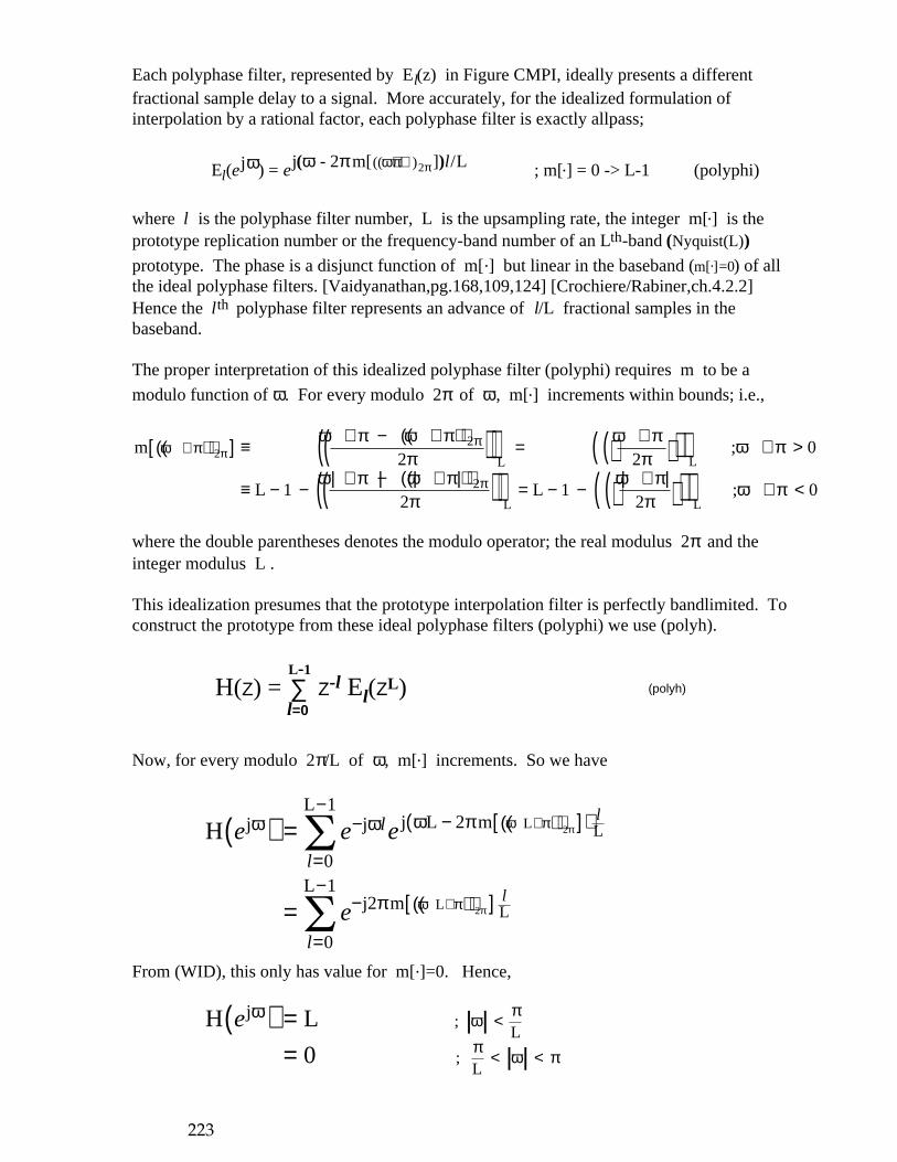
Each polyphase filter, represented by El(z) in Figure CMPI, ideally presents a differentfractional sample delay to a signal. More accurately, for the idealized formulation ofinterpolation by a rational factor, each polyphase filter is exactly allpass;
El(e jω) = e j(ω - 2π m[((ω+π))2π ])l / L ; m[.] = 0 -> L-1 (polyphi)
where l is the polyphase filter number, L is the upsampling rate, the integer m[.] is theprototype replication number or the frequency-band number of an Lth-band (Nyquist(L))prototype. The phase is a disjunct function of m[.] but linear in the baseband (m[.]=0) of allthe ideal polyphase filters. [Vaidyanathan,pg.168,109,124] [Crochiere/Rabiner,ch.4.2.2]Hence the lth polyphase filter represents an advance of l/L fractional samples in thebaseband.
The proper interpretation of this idealized polyphase filter (polyphi) requires m to be a
modulo function of ω. For every modulo 2π of ω, m[.] increments within bounds; i.e.,
( )( )[ ] ( )( )( )( ) ( )( )| | | |( )( )( )( ) | | ( )( ) 0;
21L
21L
0;22
m
<π+ωπ
π+ω−−=π
π+ω−π+ω−−≡
>π+ωπ
π+ω=π
π+ω−π+ω≡π+ω
π
π2π
LL
2
LL
2
where the double parentheses denotes the modulo operator; the real modulus 2π and theinteger modulus L .
This idealization presumes that the prototype interpolation filter is perfectly bandlimited. Toconstruct the prototype from these ideal polyphase filters (polyphi) we use (polyh).
H(Ζ) = Ζ-l El(ΖL) (polyh)∑l=0
L-1
Now, for every modulo 2π/L of ω, m[.] increments. So we have
( ) ( )( )[ ]( )
( )( )[ ]
H
=
=
e
eee
m2j
0
1L
m2Ljj
0
1Lj
π−
=
−
π−ωω−
=
−ω
l
l
l
π+ω
π+ω
L
L
2
2
π
π
l
l
L
L
From (WID), this only has value for m[.]=0. Hence,
( ) | || |0
LH
==ejω
L;
L;
π<ω<π
π<ω
223

H(Ζ) M
Figure CMPR. General model of interpolationby a rational factor.
Y(Ζ)X(Ζ) L Step Rate
Output Rate
Input Rate
E0(Ζ)
E1(Ζ)
E2(Ζ)
EL-1
(Ζ)
Figure CMPI. Ideal commutator model of interpolationshowing the many polyphase filters.
X(Ζ)
Step Rate
l
M Y(Ζ)
224

The transfer function of the commutator filter circuit in Figure CMPI (not including thedownsampler) can be described using a generalization of (polyh):
H(Ζ) = Ζ-(l - lo) El(ΖL) (polyhc)∑l=0
L-1
where lo is the starting phase of the commutator; i.e., the initial position of the brush
when the input sample x[n] arrives. The action of the downsampler170 is synchronizedto lo such that the very first sample found at position lo is passed. Reversing the brush
direction would simply change one sign of the z exponent in (polyhc); i.e., to z(l-lo) .
The individual El(z) in Figure CMPI are time-invariant and correspond to one of thecircuits shown in the Applications in Figure PL2, and Figure PA or Figure WPA (both
having the delay element connected), for the respective cases of Linear171 and ideal Allpassinterpolation. Recalling the nomenclature we previously devised for those circuits in(lipdf), we fix the coefficients of the lth filter by making the identification:τ = frac = l/L where τ is the desired fractional sample delay, frac is the polyphasefilter coefficient, l is the polyphase filter number, and L is the upsampling rate.172
By design, El(z) is a first-order two-tap non-causal FIR filter in the case of Linear interpolation;
Pl(Ζ) = (1 - l/L) + (l/L) Ζ-1
El(Ζ) = Ζ PL-l(Ζ);Linear interpolation
while in the case of ideal Allpass interpolation it is a first-order non-causal allpass filter;
1 + (1 - l/L) Ζ-1;ideal Allpass interpolation
El(Ζ) = Ζ PL-l(Ζ)
(1 - l/L) + Ζ-1
Pl(Ζ) =
170Taking the view of Crochiere, for the moment, the downsampler would operate at the steprate, L Fs .171Because the many polyphase filters of Linear interpolation require no long-term memory, wewere able to cheat in the actual implementation by using only the one circuit shown in Figure PLinstead of the entirety of Figure CMPI. Hence, we successfully implemented ideal Linearinterpolation. (We drop the term ‘ideal’ in the discussion.)172The number of polyphase filters, L, in those applications was determined by the numericalresolution of the registers holding the polyphase filter coefficients. Also note that because of the method of implementation of all the applications that we discuss,there is no division required in the capture of the coefficient, l/L.
225

1 + Ζ-1 ;ideal Allpass interpolation with coefficient warping (sw.eq)
El(Ζ) = Ζ PL-l(Ζ)
+ Ζ-1
Pl(Ζ) = (1 + l/L)(1 - l/L)
(1 + l/L)(1 - l/L)
The three Pl(z) are the respective transfer functions of the circuits in Figure PL2, Figure PA(having the delay element connected), and Figure WPA (having the delay element connected).
For the prototype interpolation filter H(z) of Linear interpolation, the length of its triangular impulseresponse is 2L as illustrated in Figure LinImpulse; that length, by design, spanning only two of theoriginal input sample periods. While in the case of ideal Allpass interpolation, the impulse responseis of infinite length as implied in Figure ALLImpulse. Both impulse responses have every Lth
sample equal to zero (except the central sample) thus identifying Lth-band (Nyquist(L)) prototype filters.[Vaidyanathan,ch.4.6] [Renfors/Saramäki] Hence the original input samples, x(n), appear unscathedat the input to the downsampler in Figure CMPI regardless of lo . A second salient characteristic of
Lth-band filters is that the frequency-shifted filter sums to level in the frequency domain like so;
( ) ( )Lk
0k
1L
=
−bhtlLWzH =
Figure LinImpulse. Impulse response of Linear interpolationprototype, L=10.
1
n0 10
h[n]
h[n]
-10 10 20 30 40n
Discrete-Time Domain Analysis
-0.4
-0.2
0.2
0.4
0.6
0.8
1
...
Figure ALLImpulse. Ideal Allpass prototype filter impulse response, L=10. [Evans]
226
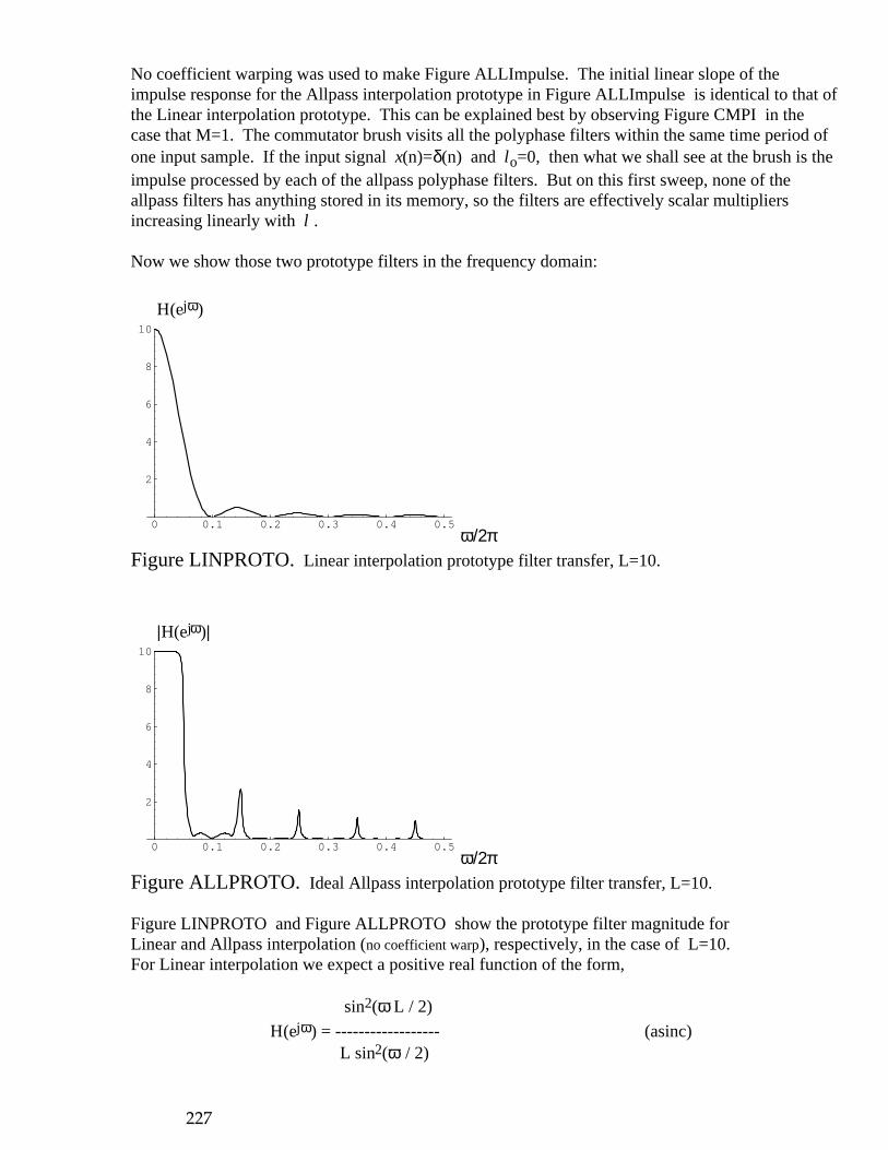
No coefficient warping was used to make Figure ALLImpulse. The initial linear slope of theimpulse response for the Allpass interpolation prototype in Figure ALLImpulse is identical to that ofthe Linear interpolation prototype. This can be explained best by observing Figure CMPI in thecase that M=1. The commutator brush visits all the polyphase filters within the same time period ofone input sample. If the input signal x(n)=δ(n) and lo=0, then what we shall see at the brush is theimpulse processed by each of the allpass polyphase filters. But on this first sweep, none of theallpass filters has anything stored in its memory, so the filters are effectively scalar multipliersincreasing linearly with l .
Now we show those two prototype filters in the frequency domain:
H(ejω)
0 0.1 0.2 0.3 0.4 0.5
2
4
6
8
10
ω/2πFigure LINPROTO. Linear interpolation prototype filter transfer, L=10.
|H(ejω)|
0 0.1 0.2 0.3 0.4 0.5
2
4
6
8
10
ω/2πFigure ALLPROTO. Ideal Allpass interpolation prototype filter transfer, L=10.
Figure LINPROTO and Figure ALLPROTO show the prototype filter magnitude forLinear and Allpass interpolation (no coefficient warp), respectively, in the case of L=10.For Linear interpolation we expect a positive real function of the form,
sin2(ω L / 2)
H(ejω) = ------------------ (asinc)L sin2(ω / 2)
227
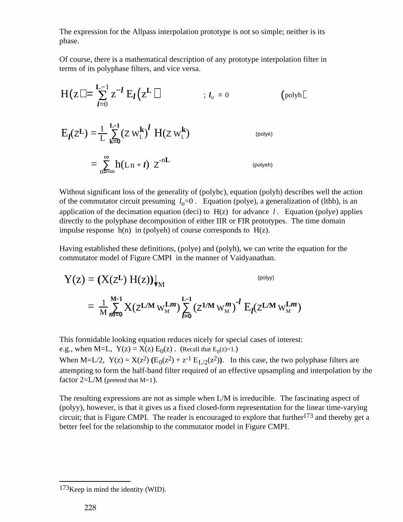
The expression for the Allpass interpolation prototype is not so simple; neither is itsphase.
Of course, there is a mathematical description of any prototype interpolation filter interms of its polyphase filters, and vice versa.
( ) ( ) ( )zEzzH = LL=
=
−hylop0;
0
1l
l
−l
lo
∑ (polye)El(ΖL) =k=0
L-1 H(Ζ WL )
k(Ζ WL )lk 1
L
∑ Ζ-nLh(Ln + l)n=-∞
∞= (polyeh)
Without significant loss of the generality of (polyhc), equation (polyh) describes well the actionof the commutator circuit presuming lo=0 . Equation (polye), a generalization of (lthb), is anapplication of the decimation equation (deci) to H(z) for advance l . Equation (polye) appliesdirectly to the polyphase decomposition of either IIR or FIR prototypes. The time domainimpulse response h(n) in (polyeh) of course corresponds to H(z).
Having established these definitions, (polye) and (polyh), we can write the equation for thecommutator model of Figure CMPI in the manner of Vaidyanathan.
El(ΖL/M WM )Lm
(polyy) Y(z) = (X(ΖL) H(z))
(Ζ1/M WM )-lm X(ΖL/M WM )
LmL-1
∑ =
M
l=0
M-1
∑m=0
1M
This formidable looking equation reduces nicely for special cases of interest: e.g., when M=L, Y(z) = X(z) E0(z) . (Recall that E0(z)=1.)
When M=L/2, Y(z) = X(z2) (E0(z2) + z-1 EL/2(z2)). In this case, the two polyphase filters areattempting to form the half-band filter required of an effective upsampling and interpolation by thefactor 2=L/M (pretend that M=1).
The resulting expressions are not as simple when L/M is irreducible. The fascinating aspect of(polyy), however, is that it gives us a fixed closed-form representation for the linear time-varyingcircuit; that is Figure CMPI. The reader is encouraged to explore that further173 and thereby get abetter feel for the relationship to the commutator model in Figure CMPI.
173Keep in mind the identity (WID).
228

Engineering Approximation to Ideal Allpass Interpolation
Rather than implement the ideal formal circuit in Figure CMPI in the case of Allpassinterpolation, our innovation (as proposed in the Applications) is to instead implement theformal circuit in Figure CMPIappx which is an approximation. The recursive elementshave been taken out of the polyphase filters in Figure CMPIappx. Now,
;Allpass interpolation Application
El(Ζ) = Ζ PL-l(Ζ)
Pl(Ζ) = (1 - l/L) + Ζ-1
As we saw in the Applications, this approximation to the ideal formulation is onlygood,174 in terms of THD+N, for microtonal changes in pitch; M/L near 1.
E0(Ζ)
M
E1(Ζ)
E2(Ζ)
EL-1
(Ζ)
Figure CMPIappx. Commutator model of proposed Allpass interpolator.
Y(Ζ)
X(Ζ)
Step Rate
l
∑Ζ-1-
l/Lx
for coefficient warping
or
(2 - l/L) l/L
174This circuit is in production in many successful electronic musical products.
229

Figure CMPIappx is the equivalent to Figure PA as is; without the feedforward delayelement connected. Each El(z) in Figure CMPIappx is nonrecursive, having no long-term memory, and time-invariant. The idea of moving the recursive part of the polyphasenetwork outside of the commutator is not new. [Crochiere/Rabiner,ch.3.4] proposedseparating out the denominator like this, but their denominator was common to all thepolyphase filters. Note that the lone time-varying recursive circuit on the right-hand sidein Figure CMPIappx only approximates the the L different time-invariant recursivecircuits that are supposed to be associated with each El(z) as in Figure CMPI.
One further refinement is our warping of the polyphase filter coefficients, computed inreal-time175 and employed in the approximation (Figure CMPIappx) to the ideal network.
;Allpass interpolation Application with coefficient warping (sw.eq)
El(Ζ) = Ζ PL-l(Ζ)
Pl(Ζ) = (1 + l/L)(1 - l/L) + Ζ-1
With warping, Figure CMPIappx becomes equivalent to Figure WPA as is. Using thisrefinement, we measured an improvement of 26 dB in THD+N for microtonal pitchchanges. (That was discussed in the Applications.)
Distortion is inherent to any interpolation process. For large pitch change with littledistortion, one’s choice (in our context) is to revert to Linear interpolation at a highsampling rate or to implement the network in Figure CMPI for ideal Allpassinterpolation. We have simulated Figure CMPI in the C programming language using16-bit polyphase filter coefficients. To achieve excellent results over a large range ofM/L for ideal Allpass interpolation, we find that coefficient warping (sw.eq) isnecessary, and that about L=28 recursive states must be stored. Since there are no time-varying coefficients in the ideal circuit of Figure CMPI, associated transient phenomenaare a non-existent component of the signal distortion characteristics. The only transientsthat arise there are due to the ZSR (Zero State Response) of the recursive polyphase filters ofAllpass interpolation. In Pitch Change/Shift applications of the ideal network, no onepolyphase filter is accessed more than another, in general. The ZSR transients will beshort for polyphase filters having small feedback coefficients, and longer for largercoefficients. So we expect ZSR transients to be evenly distributed except in degeneratecases.
Conversion: Vaidyanathan -> CrochiereThe Vaidyanathan method of analysis is simpler because it ignores changes in samplerate, whereas the method of Crochiere does not. But note that in terms of the insertion ordeletion of samples, the action of the upsampler block (as shown in Figure UV (a) and(b)) and the downsampler block (as in Figure DSB (a) and (b)) is respectively the samefor both the Crochiere and Vaidyanathan methods of analysis. While the two methods ofanalysis are equally valuable, it is prudent to have a means of converting between thetwo. Given the Vaidyanathan analysis, one simply substitutes every occurrence of zwith z’ (Crochiere’s notation) which is defined equal to zM/L , and one would re-labelany frequency domain graphs substituting ω’ (which equals ωM/L) in place of ω.
175This step is optional. Review (sw.eq) in the Applications section.
230

The conversion becomes exceedingly simple when either L or M is 1. For example,we wish to convert Figure UV (M=1, L=3) to the Crochiere-style upsampler analysis.Then we must re-label the abscissa using ω’ in place of ω, and we re-label the ordinate
as X(ejω’L) = X(ejω) in place of X(ejωL). This result is correct because Crochierealways maintains the time period between the original samples; that is true for eitherupsampling or downsampling.
Polyphase Perspectives
L H(Ζ) M
Sample Rate Conversion, Crochiere Analysis
Fs L*Fs L*Fs (L/M)*Fs
Figure CU. Contrasting the presumed computation ratesof the various methods of analysis.
(a)
L H(Ζ) M
Pitch Change by Fixed Amount, M/L
(M/L)*Fs M*Fs M*Fs Fs
(b)
L H(Ζ) M
Sample Rate Conversion, Vaidyanathan Analysis
Fs Fs Fs Fs
(c)
The sample rate conversion ratio, L/M, corresponds to the Pitch Change/Shift ratioinverse. We presume that the Pitch Change process in Figure CU (b) is performed on astored sample record. Samples appear at the input at a rate different from which theywere recorded. Such would be the case in contemporary sampler-type synthesizers.
231
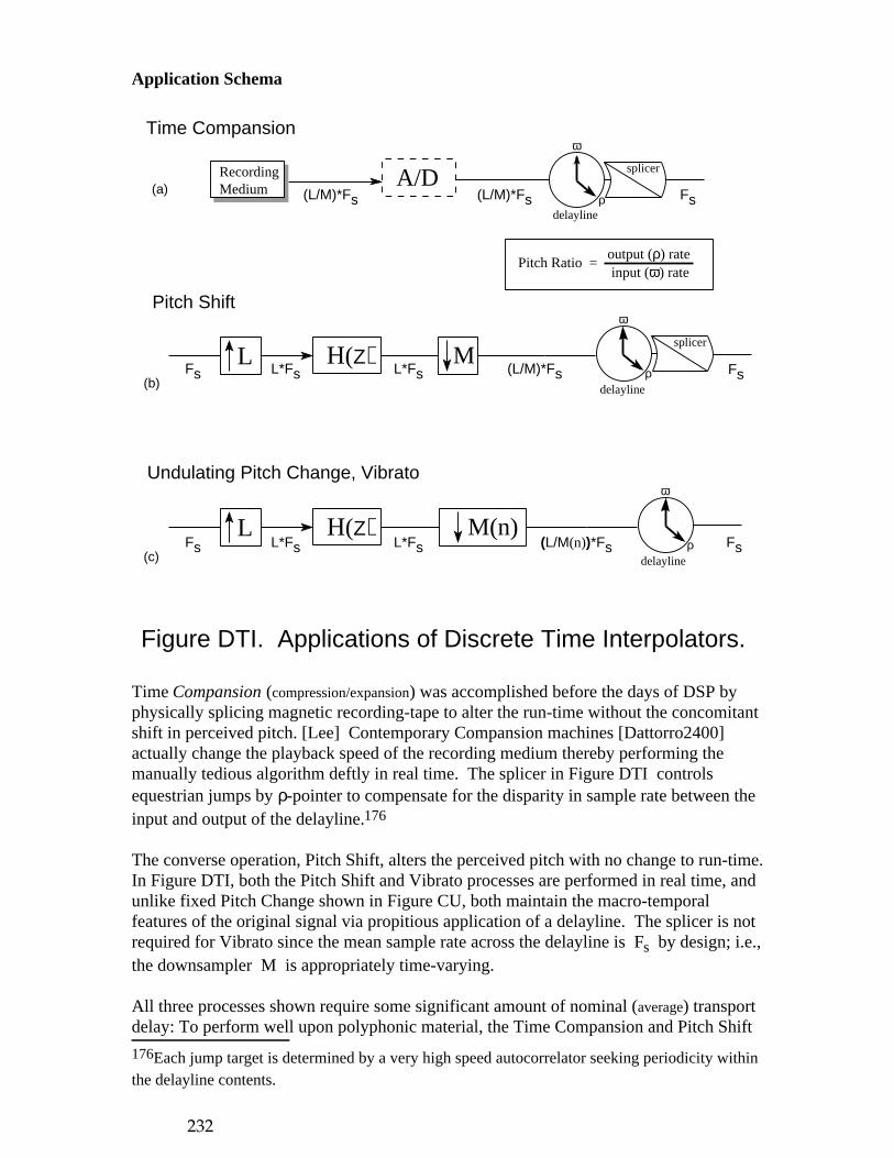
Application Schema
Figure DTI. Applications of Discrete Time Interpolators.
L H(Ζ) M
Pitch Shift
Fs L*Fs L*Fs
(L/M)*Fs
ω
delaylineρ Fs
Time Compansion
RecordingMedium
A/D(L/M)*Fs
Undulating Pitch Change, Vibrato
(a)
(b)
(c)
(L/M)*Fs Fs
ω
ρ
splicer
splicer
(L/M(n))*Fs FsL H(Ζ) M(n)
Fs L*Fs L*Fs
ω
ρ
output (ρ) rateinput (ω) rate
Pitch Ratio =
delayline
delayline
Time Compansion (compression/expansion) was accomplished before the days of DSP byphysically splicing magnetic recording-tape to alter the run-time without the concomitantshift in perceived pitch. [Lee] Contemporary Compansion machines [Dattorro2400]actually change the playback speed of the recording medium thereby performing themanually tedious algorithm deftly in real time. The splicer in Figure DTI controlsequestrian jumps by ρ-pointer to compensate for the disparity in sample rate between theinput and output of the delayline.176
The converse operation, Pitch Shift, alters the perceived pitch with no change to run-time.In Figure DTI, both the Pitch Shift and Vibrato processes are performed in real time, andunlike fixed Pitch Change shown in Figure CU, both maintain the macro-temporalfeatures of the original signal via propitious application of a delayline. The splicer is notrequired for Vibrato since the mean sample rate across the delayline is Fs by design; i.e.,the downsampler M is appropriately time-varying.
All three processes shown require some significant amount of nominal (average) transportdelay: To perform well upon polyphonic material, the Time Compansion and Pitch Shift
176Each jump target is determined by a very high speed autocorrelator seeking periodicity withinthe delayline contents.
232

algorithms require as much as 60 ms. That much delay is easily perceptible and acompromise is nearly always necessary. Vibrato, on the other hand, can be performedwell using only about 1 ms nominal delay.
Prototype Filter Design
Figure HPR. Prototype interpolation filter specs for signal bandwidth σ.
ω
L
ωp ωs
H (e ) jω
ωp ≤ minπ/M, σ/L, π/L
ωp ;π/M < σ/L
ωp + 2(π-σ)/L ;otherwiseωs =. . .. . .
Figure HPR shows the constraints on the design of the prototype filter, in general, whenabsolutely no aliasing of the signal, having (one-sided) bandwidth σ, is tolerated.177
Implicit from the axis labeling is that the desired frequency domain filter is real.
The techniques of interpolation that we considered in the Applications section did notallow this level of control over the design of the prototype. We simply accepted what theimplementation offered because it was computationally attractive.
177Note that by the filter specification in Figure HPR, there can be a discontinuity in theprogression of the allowed transition-band slope as soon as σ/L creeps just past π/M. Thathappens because the role of the prototype switches abruptly, now having the added responsibilityof further bandlimiting the signal. Admitting some small amount of aliasing mitigates that radicalchange in requirement. If σ=π, however, then the desired filter is always square.
233

Appendix XOscillator Equation DerivationRef.: Oscillator Applications
Ζ-1
Ζ-1
yq[n]
y[n]
yq[n+1]
y[n+1]
∑
∑
xεεx
-
Figure X (b). The first modified coupled form sinusoidal oscillator.
We demonstrate the derivation of the oscillator equations for one case only: the firstmodified coupled form oscillator. This analysis is adapted from [Gordon/Smith] wherethe derivation of the coupled form and the second modified coupled form is shown.
yq[n+1] = yq[n] - ε y[n]
y[n+1] = ε yq[n] + y[n]These state equations describe the ZIR of the circuit in Figure X (b). From them we readoff the matrix,
G = ( 1 -εε 1 )
If we define the vector
yn = ( yq[n]
y[n] )then we may write yn+1 = G yn . This State-Variable description has the solution,
yn = Gn yo
for all time n > 0, where Gn is called the state transition matrix, and where yo is the
vector of initial states; i.e., yn at n=0.
234

If we can find the eigenvectors and eigenvalues of G, then we may write equivalently
yn = T Λn T-1 yo
where T holds the conjugate eigenvectors (given by Mathematica) in its columns, and
Λ holds the corresponding eigenvalues along its diagonal. Specifically,
λ 0
0 λ∗Λ = ( 1 + j ε 0
0 1 - j ε ) ( )=∆
T-1 = ( -j 1 j 1 )1
2
T ( j -j1 1 )
By constructing the diagonal matrix Λ, the exponentiation no longer requires matrixmultiplication. Hence it is easier to acquire a solution analytically for large n.
The eigenvalues are the poles of the system under study. λ* denotes the conjugateeigenvalue. If we define each eigenvalue in polar form
λ = |λ| e jω∆
then we can make the identifications from Λ
1 = |λ| cos(ω)
ε = |λ| sin(ω)=>
From these we conclude
ε = sin(ω)/cos(ω)
|λ| = 1/cos(ω) ;ω < π/2. ..
where the actual oscillator coefficient ε is expressed in terms of the desired frequency ofoscillation, ω. It follows that
cosn(ω)T Λn T-1 = 1 ( sin(n ω) cos(n ω)
cos(n ω) -sin(n ω) )
235

Appendix XIESP2 Program for Linear InterpolationRef.: Interpolation Applications
! Linear interpolation of delayline: JonD, ESP2, 11/19/94.
! VoiceL[2048] (signed, 24-bit q0, left justified) is the delayline we will tap. ! The tap point will undergo modulation.
! chorus_width (unsigned GPR, q0) is the peak excursion (in samples) of the delayline! modulation about the tap point, nominal_delay.
! nominal_delay (unsigned AOR, q0) is the nominal whole sample delay into the delayline;! i.e., the center tap point.
! yqn (signed GPR, q23 (all fractional)) is the full-scale oscillator modulator output.
PROGRAM Linear
DEFCONST CLK = 40.e6 Fs = 44100. Freq = 1.0 ! Hz
Pi = 4.0*ATAN(1.0) EPSILON = 2.0*SIN((Pi*Freq)/Fs) CHORUS_WIDTH = 350 ! CHORUS_WIDTH < NOMINAL_DELAY.
NOMINAL_DELAY = 400 ! In samples. Altered to suit application.
PROGSIZE <= INT(CLK/(4.*Fs)) ! assuming one big loop
DEFREGION V VoiceL[2048] minus_one = SIZEM1V !AOR declaration = BASE modulo decrement
nominal_delay = &VoiceL[NOMINAL_DELAY] m_aor !see Style section
DEFSPR PC = LinInterp REPT_CNT = 0 SER_CONF = $007fff HARD_CONF = $008400
DEFGPR GLOBAL chorus_width = CHORUS_WIDTH epsilon = EPSILON LOCAL yqn = 0
yn = -COS((Pi*Freq)/Fs) frac=0 frac_u=0 xL vibrato=0
236
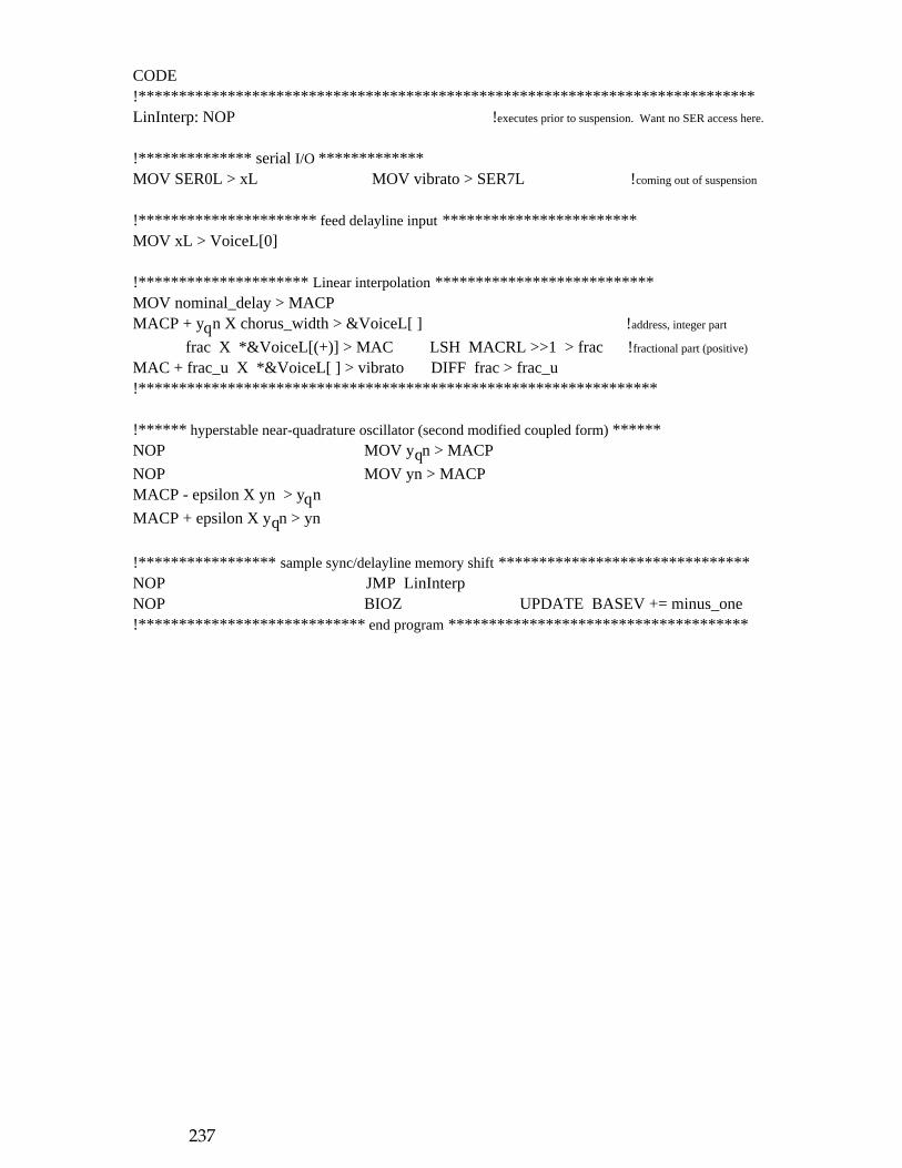
CODE!****************************************************************************LinInterp: NOP !executes prior to suspension. Want no SER access here.
!************** serial I/O *************MOV SER0L > xL MOV vibrato > SER7L !coming out of suspension
!********************** feed delayline input ************************MOV xL > VoiceL[0]
!********************* Linear interpolation ***************************MOV nominal_delay > MACP MACP + yqn X chorus_width > &VoiceL[ ] !address, integer part
frac X *&VoiceL[(+)] > MAC LSH MACRL >>1 > frac !fractional part (positive)
MAC + frac_u X *&VoiceL[ ] > vibrato DIFF frac > frac_u!****************************************************************
!****** hyperstable near-quadrature oscillator (second modified coupled form) ******NOP MOV yqn > MACP
NOP MOV yn > MACPMACP - epsilon X yn > yqn
MACP + epsilon X yqn > yn
!***************** sample sync/delayline memory shift *******************************NOP JMP LinInterpNOP BIOZ UPDATE BASEV += minus_one!**************************** end program *************************************
237

Discussion of the Linear InterpolatorAs written, the effect of this program is to produce Vibrato. For other effects, such asChorus or Flanging, slight modifications are made as discussed in the Applications.
This prototypical usage of the JMP, BIOZ, and UPDATE instructions serves as aparadigm for all sample synchronous programs employing delaylines. The delaylinememory shift via the UPDATE instruction was discussed in the section onUPDATE region BASE.
LatencyCode very similar to this Application was previously discussed in the section onComputed Addresses. There a partial AGEN listing was shown, illustrating the variouslatencies. The AGEN listing for this Application appears later on.
It is strongly recommended to place all SER data SPR access towards the beginning of aprogram in case a particular program main loop exceeds the sample period. The timemargin allowed for a program main loop to momentarily exceed the sample period is adesign feature of the BIOZ instruction; in that case there will be no BIOZ suspension onthat loop. (BIOZ is a sample-rate synchronization instruction discussed at length in the Chip Spec.)
The BIOZ instruction178 has an instruction cycle execution latency of 1. So, the first lineof our Linear interpolation program is executed prior to suspension, if suspension iswarranted.179 BIOZ is always executed before the JMP actually takes place because JMPis also one of the latent instructions. The SER data SPR transfers are latched by a transithigh of the serial interface pin signal called LRCLK. That signal is likely tied to the IOZinput pin. The IOZ pin transit high will usually take the program out of suspension. It isfor this reason that we do not place any SER data access such as
MOV SER0L > xLon the next queued program line following the BIOZ instruction (the first line of our
program), for then we would not access the most recent sample.
The first line of code appears to be wasted in our Application program. This is onlybecause of the need to simplify the presentation. It is not too difficult to find somethingfor the first program line to do which is not involved with incoming or outgoing SERaudio-sample data.180
In the portion of the code commented, !*** Linear interpolation ***, the fractions (frac andfrac_u = 1 - frac) and the address offset (&VoiceL[ ]) are all computed too late to beused in the current sample period. As long as they are all applied in the same sampleperiod, the computations will be valid, but latent.
178Any concern regarding BIOZ as the last instruction in this program is allayed by the precedingJMP.179If this program executes in an amount of time that is less than the sample period (the period ofLRCLK), then there will be suspension due to BIOZ. 180The right channel SER0R is conspicuously missing from our program; there is no reason forthis.
238

StyleInstead of the C-like notation, &VoiceL[ ], another programmer may have chosen toexplicitly declare an AOR called m_aor in region V. This may be easier toconceptualize in some cases. The interpolation code segment above would then haveappeared as follows:
!********************* Linear interpolation ******************************MOV nominal_delay > MACPMACP + yqn X chorus_width > m_aor !address, integer part
frac X *m_aor(+) > MAC LSH MACRL >>1 > frac !fractional part (positive)
MAC + frac_u X *m_aor > vibrato DIFF frac > frac_u!*******************************************************************
239
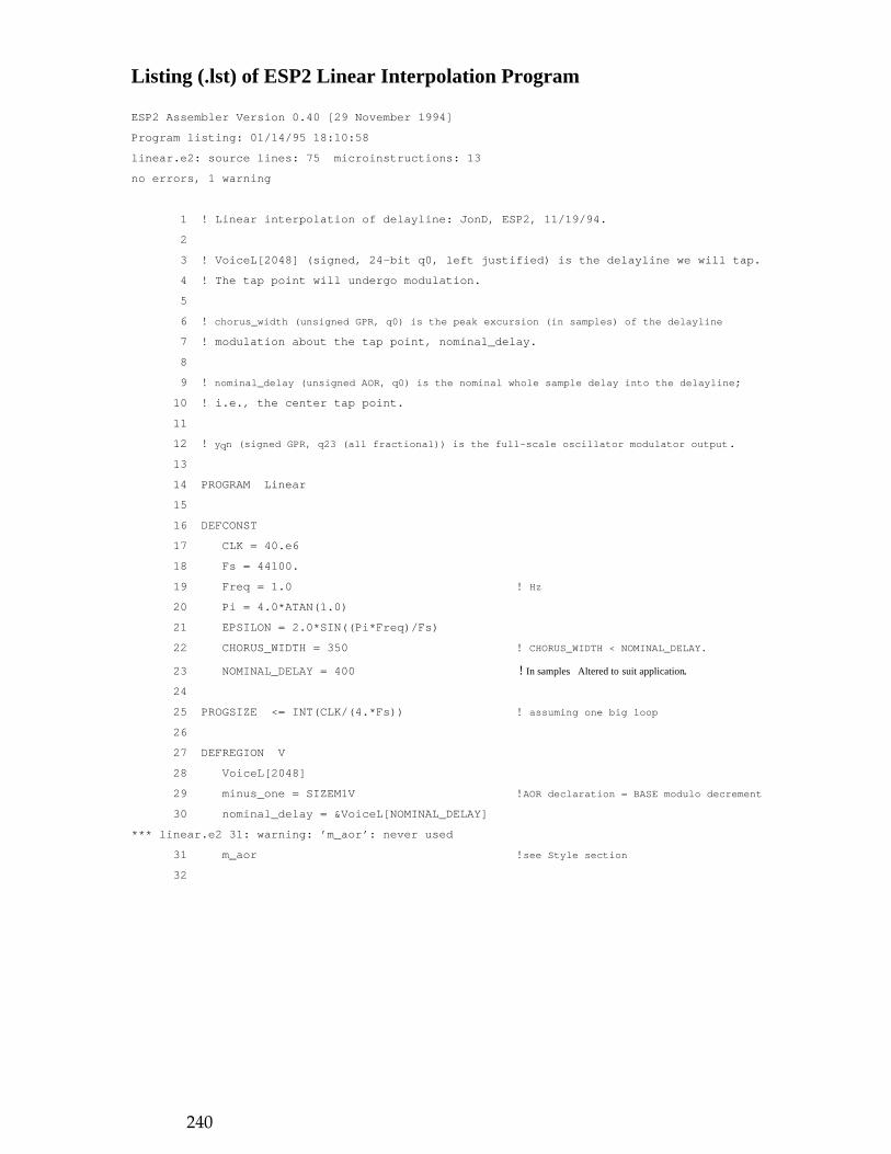
Listing (.lst) of ESP2 Linear Interpolation Program
ESP2 Assembler Version 0.40 [29 November 1994]
Program listing: 01/14/95 18:10:58
linear.e2: source lines: 75 microinstructions: 13
no errors, 1 warning
1 ! Linear interpolation of delayline: JonD, ESP2, 11/19/94.
2
3 ! VoiceL[2048] (signed, 24-bit q0, left justified) is the delayline we will tap.
4 ! The tap point will undergo modulation.
5
6 ! chorus_width (unsigned GPR, q0) is the peak excursion (in samples) of the delayline
7 ! modulation about the tap point, nominal_delay.
8
9 ! nominal_delay (unsigned AOR, q0) is the nominal whole sample delay into the delayline;
10 ! i.e., the center tap point.
11
12 ! yqn (signed GPR, q23 (all fractional)) is the full-scale oscillator modulator output.
13
14 PROGRAM Linear
15
16 DEFCONST
17 CLK = 40.e6
18 Fs = 44100.
19 Freq = 1.0 ! Hz
20 Pi = 4.0*ATAN(1.0)
21 EPSILON = 2.0*SIN((Pi*Freq)/Fs)
22 CHORUS_WIDTH = 350 ! CHORUS_WIDTH < NOMINAL_DELAY.
23 NOMINAL_DELAY = 400 ! In samples Altered to suit application.
24
25 PROGSIZE <= INT(CLK/(4.*Fs)) ! assuming one big loop
26
27 DEFREGION V
28 VoiceL[2048]
29 minus_one = SIZEM1V !AOR declaration = BASE modulo decrement
30 nominal_delay = &VoiceL[NOMINAL_DELAY]
*** linear.e2 31: warning: ’m_aor’: never used
31 m_aor !see Style section
32
240

33 DEFSPR
34 PC = LinInterp
35 REPT_CNT = 0
36 SER_CONF = $007fff
37 HARD_CONF = $008400
38
39 DEFGPR
40 GLOBAL
41 chorus_width = CHORUS_WIDTH
42 epsilon = EPSILON
43 LOCAL
44 yqn = 0
45 yn = -COS((Pi*Freq)/Fs)
46 frac=0 frac_u=0 xL vibrato=0
47
48
49 CODE
50 !****************************************************************************
000 51 LinInterp: NOP !executes prior to suspension. Want no SER access here.
52
53 !************** serial I/O *************
001 54 MOV SER0L > xL MOV vibrato > SER7L !coming out of suspension
55
56 !********************** feed delayline input **************************
002 57 MOV xL > VoiceL[0]
58
59 !********************* Linear interpolation ***************************
003 60 MOV nominal_delay > MACP
004 61 MACP + yqn X chorus_width > &VoiceL[ ] !addr,int part
005 62 frac X *&VoiceL[(+)] > MAC LSH MACRL >>1 > frac !fractional part
006 63 MAC + frac_u X *&VoiceL[ ] > vibrato DIFF frac > frac_u
64 !**********************************************************************
65
66 !****** hyperstable near-quadrature oscillator (second modified coupled form) ******
007 67 NOP MOV yqn > MACP
008 68 NOP MOV yn > MACP
009 69 MACP - epsilon X yn > yqn
00a 70 MACP + epsilon X yqn > yn
71
72 !***************** sample sync/delayline memory shift ******************************
00b 73 NOP JMP LinInterp
00c 74 NOP BIOZ UPDATE BASEV += minus_one
75 !**************************** end program ***************************************
241
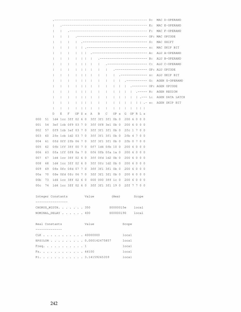
.------------------------------------------------- D: MAC D-OPERAND
| .--------------------------------------------- E: MAC E-OPERAND
| | .----------------------------------------- F: MAC F-OPERAND
| | | .------------------------------------- OP: MAC OPCODE
| | | | .---------------------------------- S: MAC SHIFT
| | | | | .-------------------------------- s: MAC SKIP BIT
| | | | | | .----------------------------- A: ALU A-OPERAND
| | | | | | | .------------------------- B: ALU B-OPERAND
| | | | | | | | .--------------------- C: ALU C-OPERAND
| | | | | | | | | .----------------- OP: ALU OPCODE
| | | | | | | | | | .-------------- s: ALU SKIP BIT
| | | | | | | | | | | .----------- G: AGEN G-OPERAND
| | | | | | | | | | | | .-------- OP: AGEN OPCODE
| | | | | | | | | | | | | .----- R: AGEN REGION
| | | | | | | | | | | | | | .--- L: AGEN DATA LATCH
| | | | | | | | | | | | | | | .- s: AGEN SKIP BIT
| | | | | | | | | | | | | | | |
D E F OP S s A B C OP s G OP R L s
000 51 1d4 1cc 3ff 02 6 0 3ff 3f1 3f1 0b 0 200 6 0 0 0
001 54 3ef 1cb 0f9 03 7 0 3ff 0f8 3e1 0b 0 200 6 0 0 0
002 57 0f9 1cb 1ef 03 7 0 3ff 3f1 3f1 0b 0 2fc 1 7 0 0
003 60 2fe 1cb 1d2 03 7 0 3ff 3f1 3f1 0b 0 2fb 4 7 0 0
004 61 0fd 0ff 2fb 06 7 0 3ff 3f1 3f1 0b 0 2fb 0 7 0 0
005 62 0fb 1ff 3ff 00 7 0 0f7 1d4 0fb 10 0 200 6 0 0 0
006 63 0fa 1ff 0f8 0a 7 0 0f6 0fb 0fa 1a 0 200 6 0 0 0
007 67 1d4 1cc 3ff 02 6 0 3ff 0fd 1d2 0b 0 200 6 0 0 0
008 68 1d4 1cc 3ff 02 6 0 3ff 0fc 1d2 0b 0 200 6 0 0 0
009 69 0fe 0fc 0fd 07 7 0 3ff 3f1 3f1 0b 0 200 6 0 0 0
00a 70 0fe 0fd 0fc 06 7 0 3ff 3f1 3f1 0b 0 200 6 0 0 0
00b 73 1d4 1cc 3ff 02 6 0 000 000 3ff 1c 0 200 6 0 0 0
00c 74 1d4 1cc 3ff 02 6 0 3ff 3f1 3f1 19 0 2ff 7 7 0 0
Integer Constants Value (Hex) Scope
-----------------
CHORUS_WIDTH. . . . . . . 350 $0000015e local
NOMINAL_DELAY . . . . . . 400 $00000190 local
Real Constants Value Scope
--------------
CLK . . . . . . . . . . . 40000000 local
EPSILON . . . . . . . . . 0.000142475857 local
Freq. . . . . . . . . . . 1 local
Fs. . . . . . . . . . . . 44100 local
Pi. . . . . . . . . . . . 3.14159265359 local
242

GPRs Address Contents (Base 10) Scope
----
chorus_width. . . . . . . $0ff $00015e 350 global
epsilon . . . . . . . . . $0fe $0004ab 1195 global
yqn . . . . . . . . . . . $0fd $000000 0 local
yn. . . . . . . . . . . . $0fc $800000 -8388608 local
frac. . . . . . . . . . . $0fb $000000 0 local
frac_u. . . . . . . . . . $0fa $000000 0 local
xL. . . . . . . . . . . . $0f9 *** *** local
vibrato . . . . . . . . . $0f8 $000000 0 local
Constant GPRs Address Contents (Base 10) Expression
-------------
ALU $005, line 62 . . . . $0f7 $ffffff -1 (???)
ALU $006, line 63 . . . . $0f6 $7fffff 8388607 (???)
External Memory Arrays Root Absolute Size Region Scope ID
----------------------
VoiceL. . . . . . . . . . $000000 $000000 2049 V local ***
AORs Address Contents (Base 10) Region Scope
----
minus_one . . . . . . . . $2ff $000800 2048 V local
nominal_delay . . . . . . $2fe $000190 400 V local
m_aor . . . . . . . . . . $2fd *** *** V local
Preset AORs Address Contents (Base 10) Region Reference
-------------
MAC $002, line 57 . . . . $2fc $000000 0 V VoiceL[0]
MAC $004, line 61 . . . . $2fb *** *** V VoiceL[ ]
SPRs Address Contents (Base 10) Scope
----
ZERO. . . . . . . . . . . $3ff *** *** local
HARD_CONF . . . . . . . . $3f3 $008400 33792 local
SER_CONF. . . . . . . . . $3f2 $007fff 32767 local
REF . . . . . . . . . . . $3f1 *** *** local
SER0L . . . . . . . . . . $3ef *** *** local
SER7L . . . . . . . . . . $3e1 *** *** local
BASEV . . . . . . . . . . $3ca $000000 0 local
SIZEM1V . . . . . . . . . $3c9 $000800 2048 local
ENDV. . . . . . . . . . . $3c8 $000800 2048 local
DIL0. . . . . . . . . . . $1ff *** *** local
DOL0. . . . . . . . . . . $1ef *** *** local
PC. . . . . . . . . . . . $1dd $000000 0 local
REPT_CNT. . . . . . . . . $1d6 $000000 0 local
MACRL . . . . . . . . . . $1d4 *** *** local
MACP_HC . . . . . . . . . $1d2 *** *** local
ONE . . . . . . . . . . . $1cc *** *** local
MINUS1. . . . . . . . . . $1cb *** *** local
243

Labels Value (Base 10)
------
LinInterp . . . . . . . . $000 0
GPR Memory Map
0/8 1/9 2/a 3/b 4/c 5/d 6/e 7/f
000 ........ ........ ........ ........ ........ ........ ........ ........
008 ........ ........ ........ ........ ........ ........ ........ ........
.
.
.
078 ........ ........ ........ ........ ........ ........ ........ ........
0/8 1/9 2/a 3/b 4/c 5/d 6/e 7/f
080 ........ ........ ........ ........ ........ ........ ........ ........
.
.
.
0f0 ........ ........ ........ ........ ........ ........ 7fffff,c ffffff,c
0f8 000000,l ******,l 000000,l 000000,l 800000,l 000000,l 0004ab,g 00015e,g
AOR Memory Map
0/8 1/9 2/a 3/b 4/c 5/d 6/e 7/f
200 ........ ........ ........ ........ ........ ........ ........ ........
208 ........ ........ ........ ........ ........ ........ ........ ........
.
.
.
278 ........ ........ ........ ........ ........ ........ ........ ........
0/8 1/9 2/a 3/b 4/c 5/d 6/e 7/f
280 ........ ........ ........ ........ ........ ........ ........ ........
288 ........ ........ ........ ........ ........ ........ ........ ........
.
.
.
2f8 ........ ........ ........ 000000,c 000000,c ******,l 000190,l 000800,l
244

Summary:
Declared Regions Base Size Available
----------------
V . . . . . . . . . . . . $000000 2049 0
Total GPRs. . . . . . . . 10 (9 initialized)
Total AORs. . . . . . . . 5 (4 initialized)
External Memory Used. . . 2049 words
Instructions Available. . 213
source lines: 75 microinstructions: 13
no errors, 1 warning
245

AGEN Listing (.agn) of ESP2 Linear Interpolation Program
! ESP2 Assembler Version 0.40 [29 November 1994]
! AGEN listing: 01/14/95 18:10:59
! linear.e2: source lines: 75 microinstructions: 13
! no errors, 1 warning
! Linear interpolation of delayline: JonD, ESP2, 11/19/94.
! VoiceL[2048] (signed, 24-bit q0, left justified) is the delayline we will tap.
! The tap point will undergo modulation.
! chorus_width (unsigned GPR, q0) is the peak excursion (in samples) of the delayline
! modulation about the tap point, nominal_delay.
! nominal_delay (unsigned AOR, q0) is the nominal whole sample delay into the delayline;
! i.e., the center tap point.
! yqn (signed GPR, q23 (all fractional)) is the full-scale oscillator modulator output.
PROGRAM Linear
DEFCONST
CLK = 40.e6
Fs = 44100.
Freq = 1.0 ! Hz
Pi = 4.0*ATAN(1.0)
EPSILON = 2.0*SIN((Pi*Freq)/Fs)
CHORUS_WIDTH = 350 ! CHORUS_WIDTH < NOMINAL_DELAY.
NOMINAL_DELAY = 400 ! In samples Altered to suit application.
PROGSIZE <= INT(CLK/(4.*Fs)) ! assuming one big loop
DEFREGION V
VoiceL[2048]
minus_one = SIZEM1V !AOR declaration = BASE modulo decrement
nominal_delay = &VoiceL[NOMINAL_DELAY]
m_aor !see Style section
DEFSPR
PC = LinInterp
REPT_CNT = 0
SER_CONF = $007fff
HARD_CONF = $008400
246

DEFGPR
GLOBAL
chorus_width = CHORUS_WIDTH
epsilon = EPSILON
LOCAL
yqn = 0
yn = -COS((Pi*Freq)/Fs)
frac=0 frac_u=0 xL vibrato=0
CODE
!****************************************************************************
LinInterp:
NOP
!************** serial I/O *************
MOV SER0L > xL MOV vibrato > SER7L
!********************** feed delayline input **************************
MOV xL > DOL0 NOP WR DOL0 > VoiceL[0]V
!********************* Linear interpolation ***************************
MOV nominal_delay > MACP NOP RD VoiceL[(+)]V > DIL0
MACP + yqn X chorus_width > &VoiceL[] NOP RD VoiceL[]V > DIL0
frac X DIL0 > MAC LSH MACRL >> 1 > frac
MAC + frac_u X DIL0 > vibrato DIFF frac > frac_u
!**********************************************************************
!****** hyperstable near-quadrature oscillator (second modified coupled form) ******
NOP MOV yqn > MACP
NOP MOV yn > MACP
MACP - epsilon X yn > yqn
MACP + epsilon X yqn > yn
!***************** sample sync/delayline memory shift ******************************
NOP JMP LinInterp
NOP BIOZ UPDATE BASEV += minus_one
!**************************** end program ***************************************
247


