84
Epitaxy and epitaxial methods

Epitaxy and epitaxial methods

What do we want to do?

What do we want to do?

Review: A.D. Yoffe, Advances in Physics 51, 799 [2002]
bulk 3D
thin films, layer structures,
quantum wells 2D
linear chain structures,
quantum wires 1D
colloids, quantum dots
0D
Dimensionality

Review: A.D. Yoffe, Advances in Physics 51, 799 [2002]
3D
2D
1D
0D
Dimensionality

Epitaxy
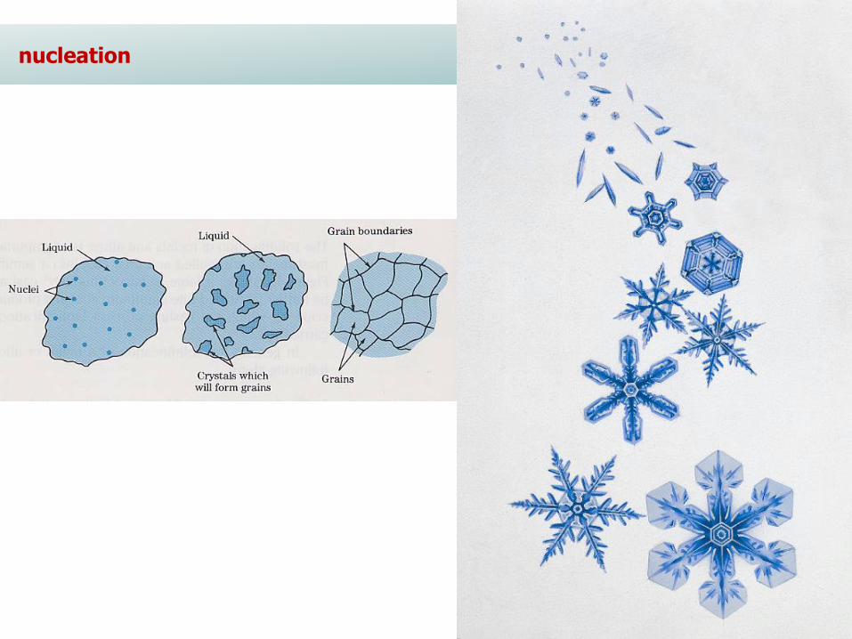
nucleation

surface processes during growth

What can we grow by MBE? What can be grown by epitaxy?

Tunneling magnetoresistance
With metals

GaN-based multiple quantum well laser diode
With semiconductors

Epitaxy:
growth of solid film on crystalline substrate
arrangement of growing atoms mimics substrate structure
Homoepitaxy:
growing layer and substrate same material
Heteroepitaxy:
growing layer differs from substrate in:
- lattice constant
- and/or crystal structure
Vocabulary

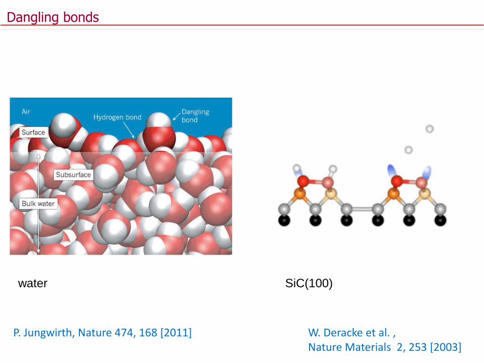
P. Jungwirth, Nature 474, 168 [2011] W. Deracke et al. , Nature Materials 2, 253 [2003]
water SiC(100)
Dangling bonds

Roughness

Atomically rough/smooth surface

Lennard-Jones potential

stress-strain
stress = force / unit area
strain = amount of
deformation an object
experiences compared to
its original size and shape
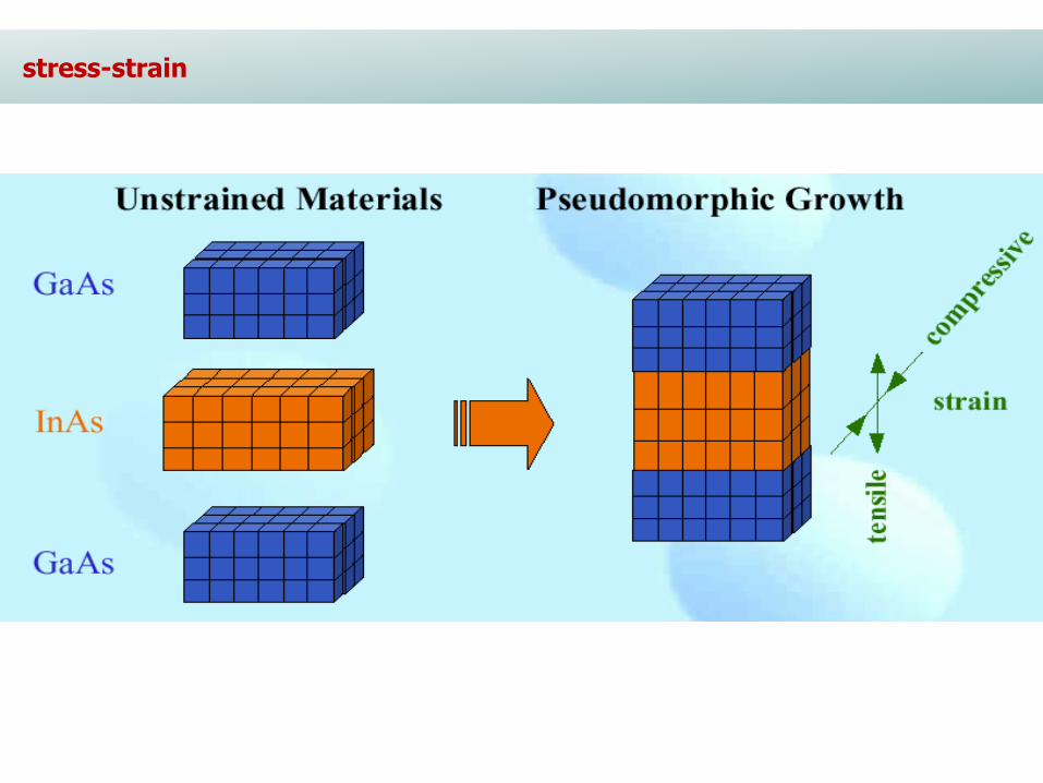
stress-strain

Lattice mismatch/misfit and related stress/strain
strain in layer
due to lattice mismatch
𝜀 =𝑎𝑠𝑢𝑏𝑠𝑡𝑟𝑎𝑡𝑒 − 𝑎𝑙𝑎𝑦𝑒𝑟
𝑎𝑠𝑢𝑏𝑠𝑡𝑟𝑎𝑡𝑒

Poisson‘s effect
material compressed in one direction,
usually tends to expand in the other
two directions perpendicular to the
direction of compression.
Poisson's ratio
= -dεtrans/dεaxial
measure of the Poisson effect
= measure of the
ratio of the fraction (or percent) of
expansion
divided by the fraction (or percent) of
compression,
for small values of these changes.

Auguste Bravais
[1845]
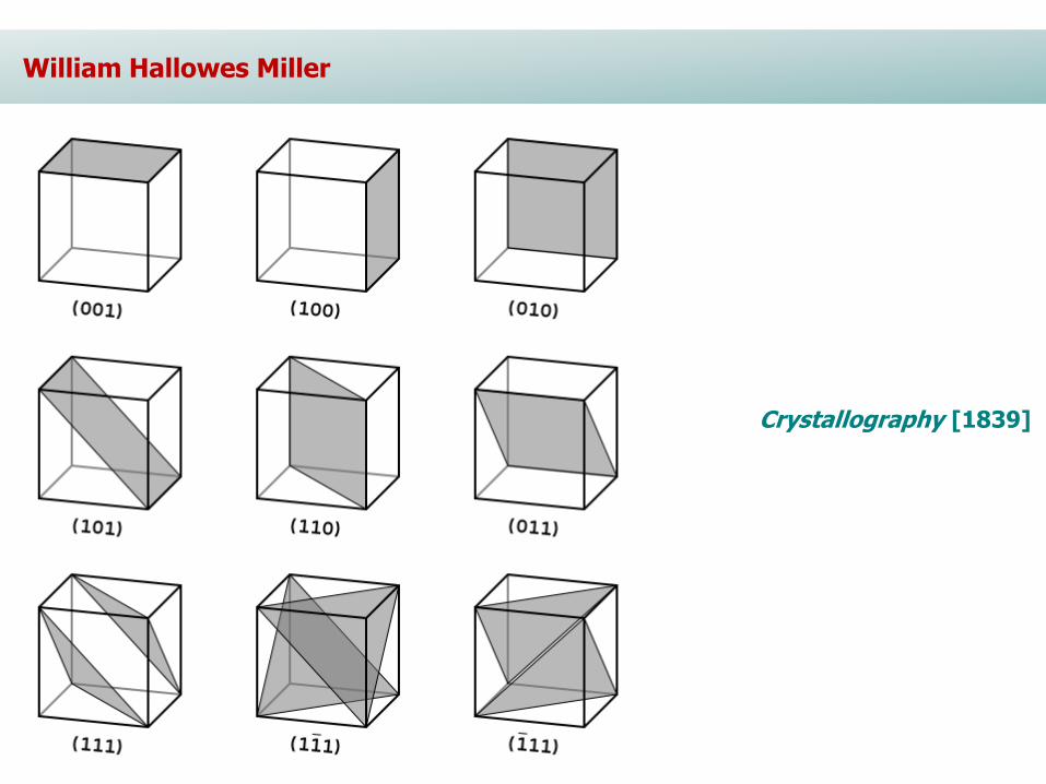
William Hallowes Miller
Crystallography [1839]

U F = U - TS Internal energy Helmholtz free energy U = energy needed to create a system F = energy needed to create a system - the energy you can get from the environment
H = U + PV G = U + PV -TS
Enthalpy Gibbs free energy H = energy needed to create a system G = total energy needed to create a + the work needed to make room for it system and make room for it – the energy you can get from the environment
thermodynamic potentials
- TS
+ P
V

wetting layer

equilibrium shapes
NaCl at 710 C
Au at 1000 C
NaCl at 620 C

equilibrium shape [facetting]
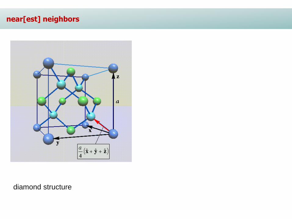
near[est] neighbors
diamond structure

K Jakobi, Prog. Surf. Sci. 71, 185 [2003]
equilibrium shape vs. substrate orientation
InAs on GaAs

equilibrium shape vs. substrate orientation - InAs on GaAs (-1-13)B

equilibrium shape vs. substrate orientation - InAs on GaAs (113)A

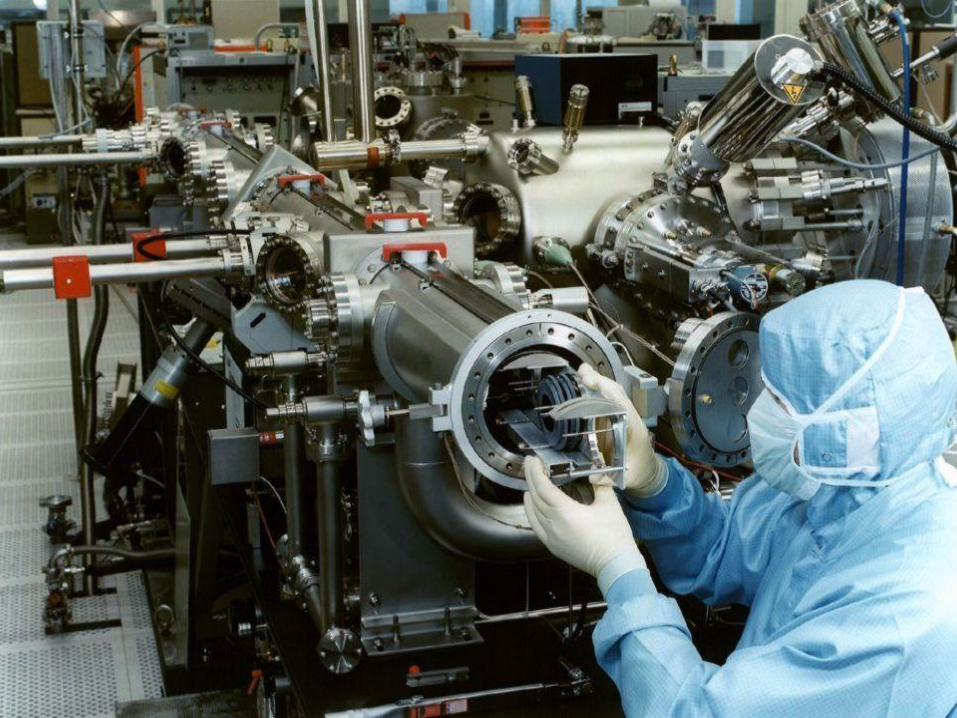
Molecular Beam Epitaxy [MBE] and the case study of SiGe/Si


Molecular Beam Epitaxy [MBE]:
▪ growth technique
▪ for fabrication of epitaxiyal layers
▪ with monolayer [ML] control
MBE principle:
▪ atoms [or clusters of atoms]
▪ produced by heating up a solid source
▪ which migrate in vacuum environment
▪ and impinge on a hot substrate
▪ where they can diffuse and eventually incorporate into the growing film
MBE

▪ vacuum deposition technique
▪ carried out in Ultra High Vacuum [UHV]:
p < 10-7 Pa
growth conditions far from thermodynamic equilibrium
▪ governed by kinetics of surface processes:
interaction impinging atoms/uppermost substrate layer
▪ precise control of beam fluxes and growth conditions
MBE MBE

MBE process MBE process

Interaction potential Interaction potential


University of Cambridge
Semiconductor Physics Group
Epitaxy and on-line monitoring

University of Cambridge
Semiconductor Physics Group
Epitaxy and on-line monitoring

Molecular Beam Epitaxy [MBE] and the case study of SiGe/Si

When special requirements are needed:
▪ interfaces abruptness and control
▪ exact doping profiles
thanks to:
▪ lower growth temperature
▪ lower growth rate
control on vacuum and sources ensures:
▪ higher purity [vs. non-UHV techniques)
▪ use of electron diffraction methods for growth control
Why to [ar not to] employ MBE Why MBE

Mass production:
MBE lower yield compared to e.g.
metalorganic Vapor Phase Epitaxy [MOVPE] beacuse of:
▪ lower growth rates
▪ lower wafer capability:
GaAs MBEmax : 4 x 6“
GaAs MOVPEmax : 5 x 10“
[up to 96 x 2“ for Si]
Why to [ar not to] employ MBE Why not MBE

1960‘s: MBE evolves from
▪ „three temperature method“
▪ surface kinetic studies of interaction Ga-As2 with GaAs
1970‘s:
▪ study of MBE surface chemical processes
▪ thermal accomodation coefficients, surface lifetimes,
desorption energies, reaction order
▪ in-situ electron diffraction techniques [RHEED]
1980‘s:
▪ introduction of gas sources
History History

1980‘s:
▪ RHEED oscillations
▪ pulsed mode
▪ multichamber systems
1990‘s-2000‘s:
▪ low dimensional heterostructures:
▪ multiple quantum wells
▪ quantum dots
▪ laser structures
History History

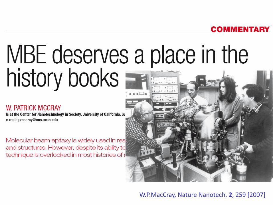
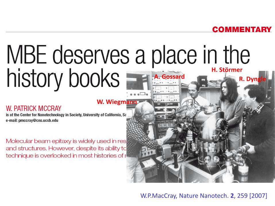
W.P.MacCray, Nature Nanotech. 2, 259 [2007]
W.P.MacCray, Nature Nanotech. 2, 259 [2007]
W.P.MacCray, Nature Nanotech. 2, 259 [2007]
W. Wiegmann
A. Gossard H. Störmer
R. Dyngle

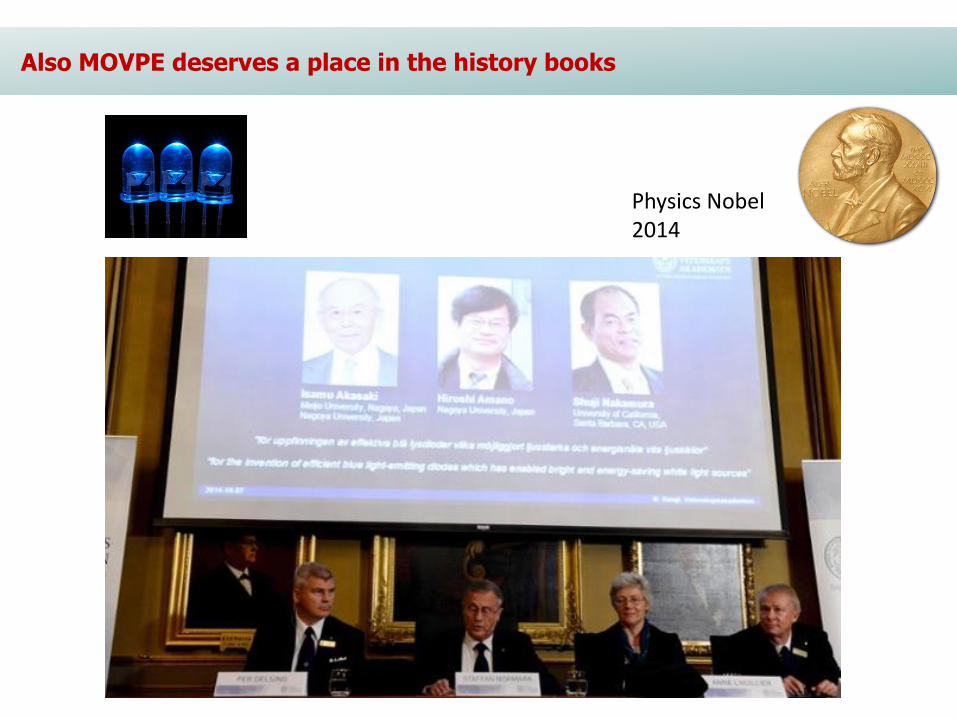
Also MOVPE deserves a place in the history books
Physics Nobel 2014
Also MOVPE deserves a place in the history books
Physics Nobel 2014

Also MOVPE deserves a place in the history books
Physics Nobel 2014

K. von Klitzing et al., Phys. Rev. Lett. 45, 494 [1980] – Nobel 1985 [quantum Hall effect]
A new era

Tsui, Strömer, and Gossard – Nobel 1998 [fractional quantum Hall effect]
K. von Klitzing et al., Phys. Rev. Lett. 45, 494 [1980] – Nobel 1985 [quantum Hall effect]
A new era

The growth chamber Growth chamber

Vacuum system:
▪ stainless-steel growth chamber
▪ UHV-connected to preparation chamber
[for substrate outgassing]
▪ load-lock module for transfer to air
All components of growth chamber must stand bake-out temperatures up to 200 °C
▪ necessary after each opening to minimize
outgassing from walls
MBE system MBE system
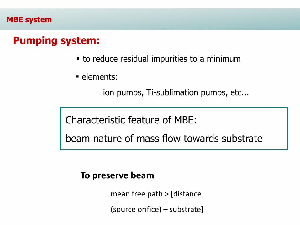
Pumping system:
▪ to reduce residual impurities to a minimum
▪ elements:
ion pumps, Ti-sublimation pumps, etc...
Characteristic feature of MBE:
beam nature of mass flow towards substrate
To preserve beam
mean free path > [distance
(source orifice) – substrate]
MBE system MBE system

Liquid N2 cryopanels:
▪ surround both chamber walls and source flange
▪ MBE cold wall technique
▪ cryopanels:
prevent re-evaporation from parts other than sources
provide thermal isulation among different sources
provide additiona pumping of residual gas
MBE system MBE system


Effusion cells Effusion cells

Effusion cells [1]:
(1) Crucible pyrolitic boron nitride, stable up to 1300 °C
(2) Ta filament for heating
(3) heat shielding Ta foils
(4) Thermocouple to measure material temperature
MBE system Effusion cells

Effusion cells [2]:
idealized Knudsen cells
▪ isothermal enclosure with small orifice
▪ evaporating surface large compared to orifice
▪ inner equilibrium pressure peq
▪ orifice < 1/10 mean free path at equilibrium
pressure
Total effusion rate:
in UHV:
MBE system Effusion cells

Effusion cells [3]:
Knudsen-type cells
small orifice
to ensure thermodynamic equilibrium melt/vapour in the cell
Langmuir-type cells [normally used]
larger orifice
wanted flux onto substrate reached with
lower cell temperature
▪ lower power consumption
▪ reduced thermal generation of impurities
MBE system Effusion cells

Inside the growth chamber Inside the growth chamber
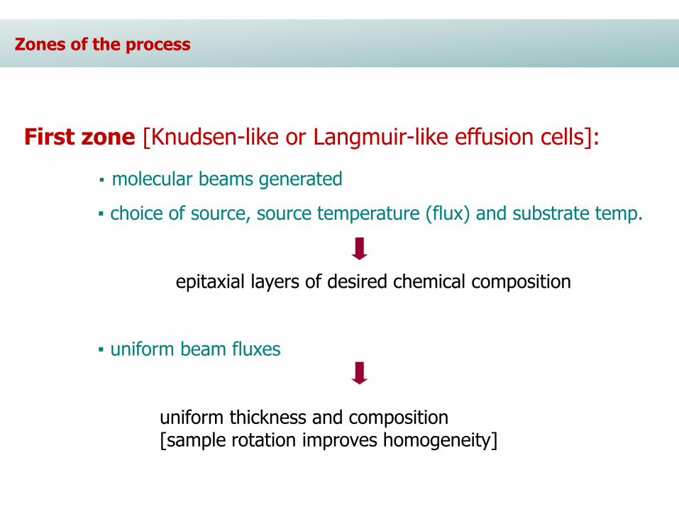
First zone [Knudsen-like or Langmuir-like effusion cells]:
▪ molecular beams generated
▪ choice of source, source temperature (flux) and substrate temp.
epitaxial layers of desired chemical composition
▪ uniform beam fluxes
uniform thickness and composition [sample rotation improves homogeneity]
MBE system: zones Zones of the process

Second zone [mixing zone]:
▪ molecular beams intersect each other
▪ mean free path of the species long enough to prevent
ineraction between different beams
Third zone [substrate surface]:
▪ site of the epitaxial growth
▪ interaction impinging species – substate
▪ adsorbtion, migration, incorporation, thermal desorption,...
MBE system: zones Zones of the process
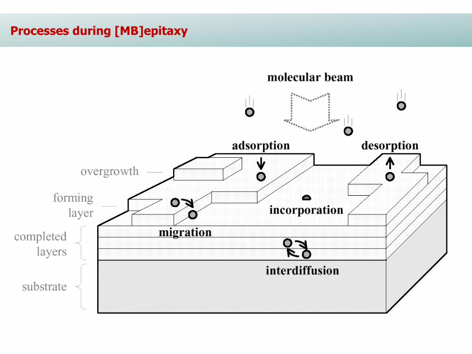
Surface processes Processes during [MB]epitaxy

layer-by-layer
Frank-van der Merwe
layer + islands
Stransky-Krastanov
islands
Volmer-Weber
Growth modes Growth modes

▪ Epitaxy from sequentially controlled surface conditions
1 atomic layer (ML) deposited per each reaction sequence
▪ digital rate control of growing surface
▪ attractive for fabrication of complex layered structures
▪ based on saturating surface reactions substrate/species
▪ each sequence: full ML or partial ML
Atomic layer epitaxy [ALE] Atomic layer epitaxy - ALE
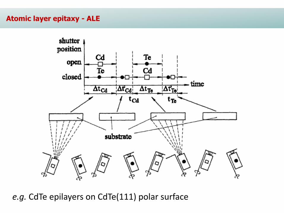
e.g. CdTe epilayers on CdTe(111) polar surface
Atomic layer epitaxy [ALE] Atomic layer epitaxy - ALE

ALE: surface processes
Atomic layer epitaxy [ALE] Atomic layer epitaxy - ALE

Deposition timing scheme for Cd1-x(Zn,Mn) x Te ALE
Atomic layer epitaxy [ALE] Atomic layer epitaxy - ALE

diffusion implantation epitaxy
▪ simple process
▪ everything
diffuses
▪ high
concentrations
▪ lattice damage
▪ intact lattice
▪ low
concentrations
Doping doping

What can we grow by MBE? What can be grown by MBE?
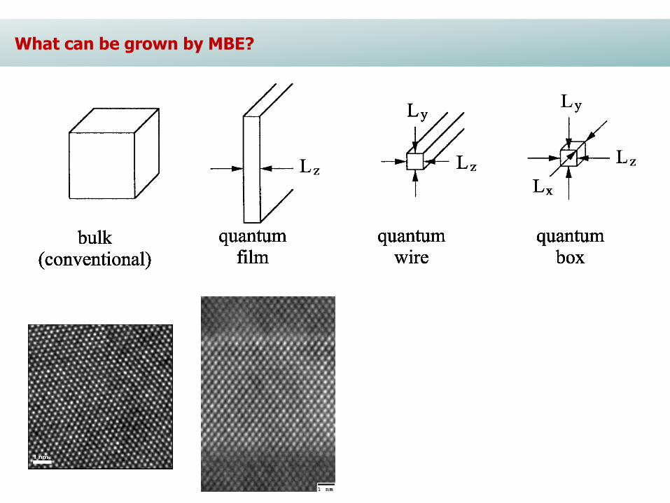
What can we grow by MBE? What can be grown by MBE?

What can we grow by MBE? What can be grown by MBE?

What can we grow by MBE? What can be grown by MBE?

M. Kalahdouz et al., Appl. Phys. Lett. 96, 213516 [2010]
QD in the structure
improved performance of IR thermal detectors
And combined structures And combined structures

Z.M.Wang et al., Appl.Phys.Lett. 84, 1931 [2004]
InGaAs quantum dots on GaAs

G.Springholz et al., Science 282, 734 [1998]
Self assembling and self ordering in PbSe
[vertically aligned]
quantum dots

ZnTe and ZnMnTe nanostructures on CdTe
A.Bonanni et al., Appl.Phys.Lett. 74, 3732 [1999]
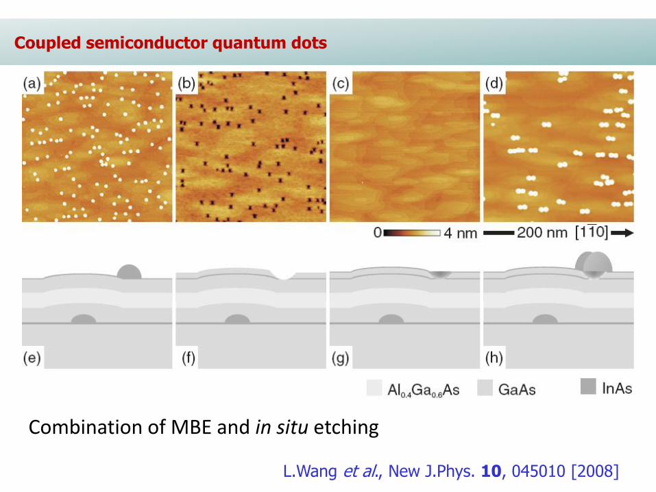
L.Wang et al., New J.Phys. 10, 045010 [2008]
Combination of MBE and in situ etching
Coupled semiconductor quantum dots Coupled semiconductor quantum dots


