Page 1
Takashi Hayakawa / Tokyo Electron Limited / March 18th, 2015
TM
Equipment and Process Technologies
for 3D Structural Devices
Semicon China2015, Equipment & Material Forum, March 18th, 2015
Takashi Hayakawa
Senior Manager / SPE Marketing Department
Tokyo Electron Limited
Page 2
Takashi Hayakawa / Tokyo Electron Limited / March 18th, 2015
TM
• TEL China Introduction
• Further Scaling Scenario
– Technology Trend
– Tool Supplier’s Challenges & Opportunities
• Equipment & Process Technology
– Wet Technology (Prevent Pattern Collapse)
– Dry Etch Technology (SAC & Defect Reduction)
• Summary & Message
Outline
Page 3
Takashi Hayakawa / Tokyo Electron Limited / March 18th, 2015
TM
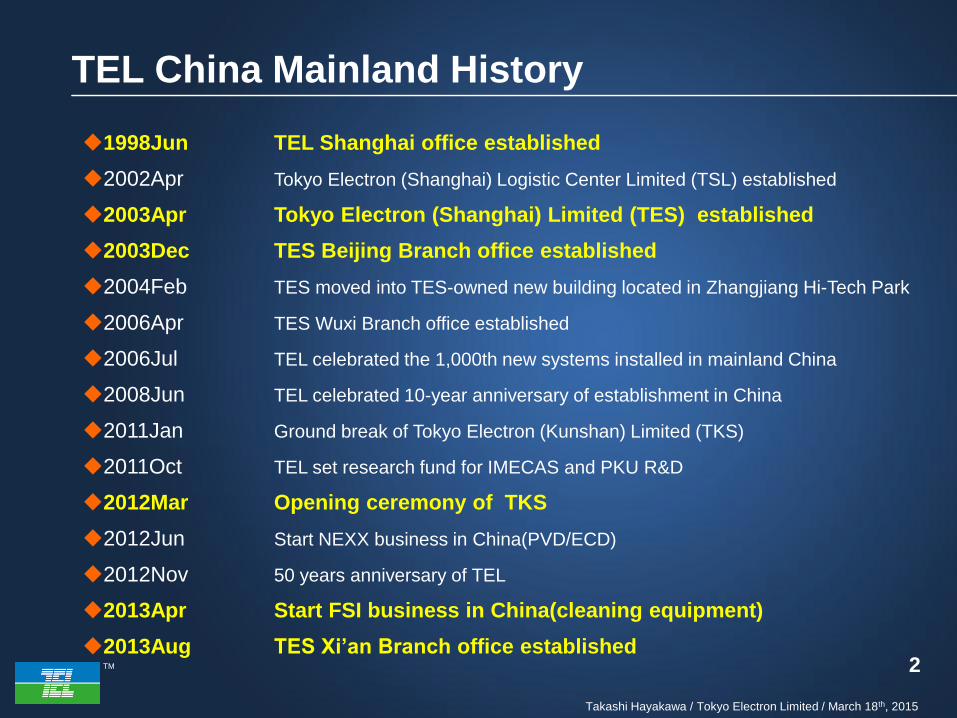
TEL China Mainland History
2
1998Jun TEL Shanghai office established
2002Apr Tokyo Electron (Shanghai) Logistic Center Limited (TSL) established
2003Apr Tokyo Electron (Shanghai) Limited (TES) established
2003Dec TES Beijing Branch office established
2004Feb TES moved into TES-owned new building located in Zhangjiang Hi-Tech Park
2006Apr TES Wuxi Branch office established
2006Jul TEL celebrated the 1,000th new systems installed in mainland China
2008Jun TEL celebrated 10-year anniversary of establishment in China
2011Jan Ground break of Tokyo Electron (Kunshan) Limited (TKS)
2011Oct TEL set research fund for IMECAS and PKU R&D
2012Mar Opening ceremony of TKS
2012Jun Start NEXX business in China(PVD/ECD)
2012Nov 50 years anniversary of TEL
2013Apr Start FSI business in China(cleaning equipment)
2013Aug TES Xi’an Branch office established
Page 4
Takashi Hayakawa / Tokyo Electron Limited / March 18th, 2015
TM
TEL China Mainland Operations
3 东电电子(上海)有限公司 东电电子(北京)分公司 东电电子(无锡)分公司 东电电子(西安)分公司 东电光电半导体设备(昆山)有限公司
北京
大连
上海
无锡
成都 武汉 昆山
厦门
深圳
西安
Head Office
Branch
Manufacture
Service Site
Parts Center
(As of Dec31, 2014)
Shanghai Beijing Wuxi Xi’an Kunshan
Page 5
Takashi Hayakawa / Tokyo Electron Limited / March 18th, 2015
TM
Functional Diversification
CM
OS
Scali
ng
FEOL
Strained Si
High-k
Metal Gate
FinFET
Patterning
ArF
ArF
Immersion
EUV
Source :TEL based on ITRS
DP/MP
SiGe
NIL
Flip-Chip
Wire-Bonding
DRAM
NAND
STT-MRAM
ReRAM
Memory
DSA
Semiconductor Technology Divergence
SiCOH
~2.7
FSG
Cu
SiCOH
~2.5
Metal Hardmask III-V
SOD
Air Gap
SiCOH
~2.2
HMC
MIS Contact
TFET
Post Cu Metal
CNT
Spin Transistor
BEOL
Cap Metal
Si Photonics
EB
3DI
Ge
Nanowire
3D NAND
PCRAM
NOR
2.5D
SAC
Mo
re M
oo
re
Advanced Packaging
More than Moore
Page 6
Takashi Hayakawa / Tokyo Electron Limited / March 18th, 2015
TM
FinFET Formation
Does FinFET require more process steps???
download.intel.com/newsroom/kits/22nm/pdfs/22nm-Announcement_Presentation.pdf
Page 7
Takashi Hayakawa / Tokyo Electron Limited / March 18th, 2015
TM
FinFET Process Flow Comparison 2
D P
lan
ar
Fin
FE
T
STI Ox CMP STI Ox Recess SiN Removal
STI Ox CMP STI Ox Recess &
Gate Height Control SiN Removal
Fin Corner
Rounding Sac-Ox Removal
# Process (Difference e.g. 32nm vs 22nm)
1 STI Ox Recess & Gate Height Control
2 Fin Corner Rounding
3 Sacrificial Ox Removal
4 Doping (Plasma Doping or Solid Phase Doping)
5 SAC (Self Align Contact)
6 Double Patterning
Few more process are needed for FinFET formation
Page 8
Takashi Hayakawa / Tokyo Electron Limited / March 18th, 2015
TM
Scaling Cost Challenges
(Source: ARM) (Source: NVIDIA)
(Source: AMD)
The Fabless community openly discuss concerns about cost…
Page 9
Takashi Hayakawa / Tokyo Electron Limited / March 18th, 2015
TM
Functional Diversification
CM
OS
Scali
ng
FEOL
Strained Si
High-k
Metal Gate
FinFET
Patterning
ArF
ArF
Immersion
EUV
Source :TEL based on ITRS
SiGe
NIL
Flip-Chip
Wire-Bonding
DRAM
NAND
STT-MRAM
ReRAM
Memory
DSA
Semiconductor Technology Divergence
SiCOH
~2.7
FSG
Cu
SiCOH
~2.5
Metal Hardmask III-V
SOD
Air Gap
SiCOH
~2.2
HMC
MIS Contact
TFET
Post Cu Metal
CNT
Spin Transistor
BEOL
Cap Metal
Si Photonics
EB
3DI
Ge
Nanowire
3D NAND
PCRAM
NOR
Expanding Requirements : Scaling, Structure/Material
2.5D
SAC
DP/MP
Mo
re M
oo
re
Advanced Packaging
More than Moore
Page 10
Takashi Hayakawa / Tokyo Electron Limited / March 18th, 2015
TM
Inflection Point in Patterning (2D 1D)
90nm (Planar Poly Gate)
PMOS
T. Ghani, et al.,
IEDM 2003
45nm (Planar RMG)
K. Mistry, et al.,
IEDM 2003
PMOS
22nm (FinFET RMG)
C. Auth et al.,
VLSI tech. 2012
Kelin J. Kuhn, IEDM 2007
Kelin J. Kuhn, IEDM 2007
STI Gate Contact 1 Contact 2
1D
1D + Cut
SADP + Cut SADP + Cut (x1 – 2)
2-Level Local Interconnect
2-Level Local Interconnect
LELE
LELELE
Layout
NA
.
C-H Jan, et al., IEDM 2012
There is design simplification together with processing complexity
Page 11
Takashi Hayakawa / Tokyo Electron Limited / March 18th, 2015
TM
32nm 10nm 7nm
Active 193i 1 SADP + Cut 1+1 SAQP + LE2 Cut 1+2
Gate 193i + Cut 1+1 SADP + Cut 1+1 SADP + Cut 1+1
Contact 193i + 193i 2 LE2+LE2 4 LE2 + LE3 5
Via 0 193i 1 LE2 2 LE3 3
Metal 1 193i + Cut 1+1 LE3 3 SADP + LE3 Block 1+3
Via 1 193i 1 LE2 2 LE4 4
Metal 2 193i + Cut 1+1 SADP + Block 1+1 SAQP + LE3 Block 1+3
Mask Count 12 Mask Count 17 Mask Count 25
Self-Aligned Multiple Patterning
Doubling Cutting litho Final Core litho
Gate Metal 1
Doubling Blocking litho Final Core litho
Source: Julien R, IMEC
SaMP also increase process complexity
Page 12
Takashi Hayakawa / Tokyo Electron Limited / March 18th, 2015
TM
Extendability of SADP
SAQP
40 nm hp 20 nm hp 12.5 nm hp
SAOP SADP
40 nm hp 20 nm hp 10 nm hp 5 nm hp
PR
193i Single
Patterning
7.3 nm hp
SAOP : Self-Aligned Octuple Patterning
Ox
Because of EUV introduction delay,
SaDP can be extended to 4x and 8x pitch multiplication
Page 13
Takashi Hayakawa / Tokyo Electron Limited / March 18th, 2015
TM
Edge Placement Error in SA Multi Patterning
𝑬𝑷𝑬𝐺𝑟𝑖𝑑 + 𝑐𝑢𝑡 = 𝑓(𝐶𝐷𝑈𝐺𝑟𝑖𝑑, 𝐿𝐸𝑅𝐺𝑟𝑖𝑑, 𝐿𝐶𝐷𝑈𝐺𝑟𝑖𝑑, 𝑂𝐿𝐶𝑢𝑡, 𝐶𝐷𝑈𝐶𝑢𝑡, 𝐶𝐸𝑅𝐶𝑢𝑡, 𝐿𝐶𝐷𝑈𝐶𝑢𝑡)
PAST:
Single pattern variation defined
by CDU, overlay and LWR
FUTURE:
Multiple pattern variation defined by
Edge Placement Error (EPE)
2
2
2
Multiple patterning increases variability (2x, 3x…more)
Page 14
Takashi Hayakawa / Tokyo Electron Limited / March 18th, 2015
TM
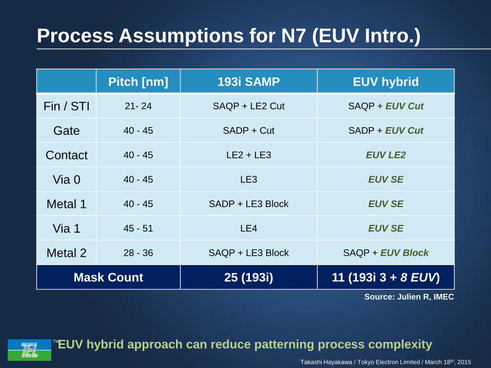
Process Assumptions for N7 (EUV Intro.)
Pitch [nm] 193i SAMP EUV hybrid
Fin / STI 21- 24 SAQP + LE2 Cut SAQP + EUV Cut
Gate 40 - 45 SADP + Cut SADP + EUV Cut
Contact 40 - 45 LE2 + LE3 EUV LE2
Via 0 40 - 45 LE3 EUV SE
Metal 1 40 - 45 SADP + LE3 Block EUV SE
Via 1 45 - 51 LE4 EUV SE
Metal 2 28 - 36 SAQP + LE3 Block SAQP + EUV Block
Mask Count 25 (193i) 11 (193i 3 + 8 EUV)
Source: Julien R, IMEC
EUV hybrid approach can reduce patterning process complexity
Page 15
Takashi Hayakawa / Tokyo Electron Limited / March 18th, 2015
TM
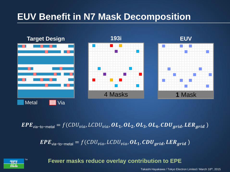
EUV Benefit in N7 Mask Decomposition
193i
4 Masks
EUV
1 Mask
Target Design
Metal Via
𝑬𝑷𝑬via−to−metal = 𝑓(𝐶𝐷𝑈𝑣𝑖𝑎, 𝐿𝐶𝐷𝑈𝑣𝑖𝑎 , 𝑶𝑳𝟏, 𝑶𝑳𝟐, 𝑶𝑳𝟑, 𝑶𝑳𝟒, 𝑪𝑫𝑼𝒈𝒓𝒊𝒅, 𝑳𝑬𝑹𝒈𝒓𝒊𝒅 )
𝑬𝑷𝑬via−to−metal = 𝑓(𝐶𝐷𝑈𝑣𝑖𝑎, 𝐿𝐶𝐷𝑈𝑣𝑖𝑎, 𝑶𝑳𝟏, 𝑪𝑫𝑼𝒈𝒓𝒊𝒅, 𝑳𝑬𝑹𝒈𝒓𝒊𝒅 )
Fewer masks reduce overlay contribution to EPE
Page 16
Takashi Hayakawa / Tokyo Electron Limited / March 18th, 2015
TM
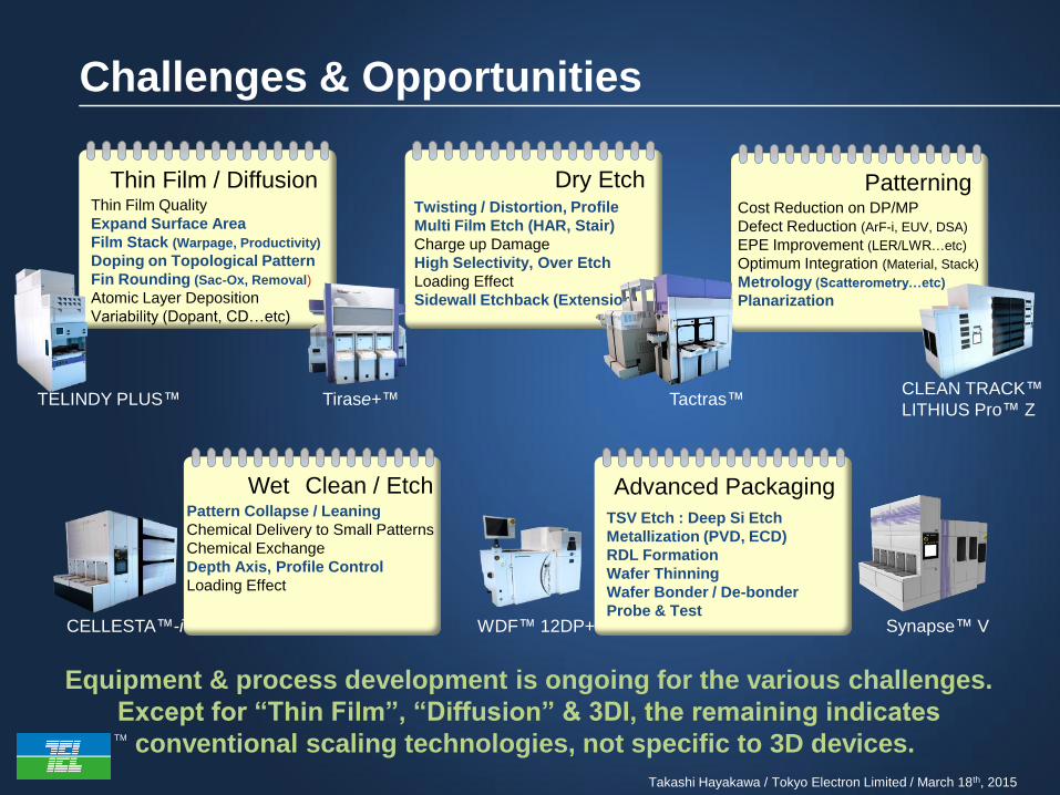
Challenges & Opportunities
Pattern Collapse / Leaning
Chemical Delivery to Small Patterns
Chemical Exchange
Depth Axis, Profile Control
Loading Effect
Wet Clean / Etch
Thin Film Quality
Expand Surface Area
Film Stack (Warpage, Productivity)
Doping on Topological Pattern
Fin Rounding (Sac-Ox, Removal)
Atomic Layer Deposition
Variability (Dopant, CD…etc)
Thin Film / Diffusion Twisting / Distortion, Profile
Multi Film Etch (HAR, Stair)
Charge up Damage
High Selectivity, Over Etch
Loading Effect
Sidewall Etchback (Extension)
Dry Etch Cost Reduction on DP/MP
Defect Reduction (ArF-i, EUV, DSA)
EPE Improvement (LER/LWR…etc)
Optimum Integration (Material, Stack)
Metrology (Scatterometry…etc)
Planarization
Patterning
TSV Etch : Deep Si Etch
Metallization (PVD, ECD)
RDL Formation
Wafer Thinning
Wafer Bonder / De-bonder
Probe & Test
Advanced Packaging
Equipment & process development is ongoing for the various challenges.
Except for “Thin Film”, “Diffusion” & 3DI, the remaining indicates
conventional scaling technologies, not specific to 3D devices.
TELINDY PLUS™ Tirase+™ Tactras™ CLEAN TRACK™
LITHIUS Pro™ Z
CELLESTA™-i Synapse™ V WDF™ 12DP+
Page 17
Takashi Hayakawa / Tokyo Electron Limited / March 18th, 2015
TM
• Almost all CMOS devices have adapted to 3D
structure, Capacitor, 3D NAND, FinFET…
• In parallel, scaling centric tool & process
development with economical cost is
important
Short Summary of Further Scaling Scenario
Productivity
Scaling
Performance
Page 18
Takashi Hayakawa / Tokyo Electron Limited / March 18th, 2015
TM
Mechanism of Pattern Collapse
Fluid on Wafer Evaporation of Fluid Pattern Collapse
Ref. : ECS2013, Advanced wafer drying technology for 1x node and beyond using Surface Modification Method
・ΔP = P2 – P1
・ΔP = γ/R = 2γcosθ/S
γ : Surface tension,
R : Radius of curvature
<Laplace Pressure>
・F = ( 2γcosθ/S ) *H*D
<Pattern Collapse Force>
Collapse force can be controlled by surface condition & hydrophobicity
Page 19
Takashi Hayakawa / Tokyo Electron Limited / March 18th, 2015
TM
Chemical Drying Method Comparison
Liquid IPA F-Solvent SMM**
Final Drying Liquid IPA HFE Water
*Surface Tension(mN/m) 22 14 73
Contact Angle(°)@SiO2 10 (0.98) 10 (0.98) 92 (-0.035)
* Value 20°C, **SMM : Surface Modification Method ( ) =cosθ
Pattern Feature :
Vertical line and space pattern with 18nm width
(1: 1 pitch, 2 dimensions)
Patterning substrate : Si (Young’s modulus : 112[GPa])
Ref. : ECS2013, Advanced wafer drying technology for 1x node and beyond using Surface Modification Method
Surface Modification Method successfully prevents failure due to collapse
Page 20
Takashi Hayakawa / Tokyo Electron Limited / March 18th, 2015
TM
Surface Modification Agent Reaction
Chemical Oxide
Si
θ
θ
Surface
Modification Agent Water
Modification
Agent Chemical
MAC is replaced by DIW
without drying
Drying
Ref. : ECS2013, Advanced wafer drying technology for 1x node and beyond using Surface Modification Method
Initial Post SMM
SMM
Control contact angle, cosθ = ~1.0, minimize collapse force
Page 21
Takashi Hayakawa / Tokyo Electron Limited / March 18th, 2015
TM
Experimental Results Ref.: ECS2013, Advanced wafer drying technology for 1x node and beyond using Surface Modification Method
Surface Modification Method:
Process time 120sec
Poly Si SiO2 SiN
Conventional (Liquid IPA dry)
Surface Modification Method
Surface modification method is effective in minimizing the failure
Page 22
Takashi Hayakawa / Tokyo Electron Limited / March 18th, 2015
TM
Etch Challenges : SAC (Self-Aligned Contact) 2
D P
lan
ar
Fin
FE
T
STI Ox CMP STI Ox Recess SiN Removal
STI Ox CMP STI Ox Recess &
Gate Height Control SiN Removal
Fin Corner
Rounding Sac-Ox Removal
# Process (Difference e.g. 32nm vs 22nm)
1 STI Ox Recess & Gate Height Control
2 Fin Corner Rounding
3 Sacrificial Ox Removal
4 Doping (Plasma Doping or Solid Phase Doping)
5 SAC (Self Aligned Contact)
6 Double Patterning
22nm & beyond technologies require SAC process
Page 23
Takashi Hayakawa / Tokyo Electron Limited / March 18th, 2015
TM
Model of SiO2 Selective Etch Over Si3N4 Ref. : AVS2014 Dielectric Etch Challenges and Evolutions
SEM Images : Wafer Temp. Split (Condition = CxFy/Ar/O2 Chemistry)
Higher wafer temperature condition is one of the effective solution to
suppress SiN shoulder loss during SAC etching
Page 24
Takashi Hayakawa / Tokyo Electron Limited / March 18th, 2015
TM
Investigation of Selectivity Difference Ref. : AVS2014 Dielectric Etch Challenges and Evolutions
At higher wafer temp., fluorocarbon (FC) deposition thickness on SiO decreases,
while FC deposition thickness on SiN is almost kept. In addition, C/F ratio
become higher, as wafer temp. become higher.
Atomic composition observed by XPS
Split : wafer temperature
TEM Images : SiO2 & SiN Surface, Split Wafer Temp.
Page 25
Takashi Hayakawa / Tokyo Electron Limited / March 18th, 2015
TM
To Realize Furthermore Highly Selective Etch Ref. : AVS2014 Dielectric Etch Challenges and Evolutions
ALE, Atomic Layer Etch, is one of the powerful candidate to realize ultra highly
selective SiO2 etching in SAC, because ALE has a strong potential to control the
thinner CF polymer and lower ion energy precisely in principle
JVST A 13(3), 1996, Athavale, Economou et al.
JVST A 32(2), 2014, D.Metzler, R.Bruce, S.Engelmann, E.
Joseph, Oehrlein.
JVST A 27(1), 2009,
Agarwal, Kushner et al.
JVST A 31(6), 2013, Park, Yeom et al.
Page 26
Takashi Hayakawa / Tokyo Electron Limited / March 18th, 2015
TM
New Technology : Quasi-ALE for SAC Ref. : AVS2014 Dielectric Etch Challenges and Evolutions
Separation of radical adsorption and ion bombardment step enables
independent control of radical and ion flux. With this scheme, precise control of
surface reaction layer by layer becomes possible by controlling process time.
Active by
Ion bombardment
+ + +
Ion Irradiation
(Only Ion w/o radical)
Γi:1E14-16 [cm-2]
Reactant Feed
Adsorb FC film
Radical
Transportation
Γr:1E14-16[cm-2]
Time
Initial
Si [100]:
6.8E14 [atoms/cm2]
Desorption
x N
Reaction of FC depo isn’t self-limited, so not mono layer but several atomic layers adsorb
in accordance with time and plasma condition of the adsorption step.
So we named this process “Quasi-ALE”.
Page 27
Takashi Hayakawa / Tokyo Electron Limited / March 18th, 2015
TM
Feasibility Study : Quasi-ALE for SAC Ref. : AVS2014 Dielectric Etch Challenges and Evolutions
Trade off relationship between SiO2 etch through capability and SiN loss amount
is improves by Quasi-ALE process
Quasi-ALE
0
10
20
30
40
50
60
70
0 50 100
Etch
am
ou
nt
[nm
]
Etch time [sec.]
SiO2
SiN
Conventional
CxFy/Ar/O2 Chemistry
Page 28
Takashi Hayakawa / Tokyo Electron Limited / March 18th, 2015
TM
Quasi-ALE Process Demonstration Ref. : AVS2014 Dielectric Etch Challenges and Evolutions
Quasi-ALE process shows the best SiN loss performance with keeping good
etch through capability on slit pattern compared to conventional one. ALE is one
of the strong candidate to overcome the issues related selectivity.
Conventional Method
Quasi-ALE
Post Ash Post HF dip
Post Ash Post HF dip Post Etch
SiN loss
3.5/5.6nm
Page 29
Takashi Hayakawa / Tokyo Electron Limited / March 18th, 2015
TM
Functional Diversification
CM
OS
Scali
ng
FEOL
Strained Si
High-k
Metal Gate
FinFET
Patterning
ArF
ArF
Immersion
EUV
Source :TEL based on ITRS
DP/MP
SiGe
NIL
Flip-Chip
Wire-Bonding
DRAM
NAND
STT-MRAM
ReRAM
Memory
DSA
Summary & Message
SiCOH
~2.7
FSG
Cu
SiCOH
~2.5
Metal Hardmask III-V
SOD
Air Gap
SiCOH
~2.2
HMC
MIS Contact
TFET
Post Cu Metal
CNT
Spin Transistor
BEOL
Cap Metal
Si Photonics
EB
3DI
Ge
Nanowire
3D NAND
PCRAM
NOR
Expanding Requirements : Scaling, Structure/Material, 450mm
2.5D
SAC
Mo
re M
oo
re
Advanced Packaging
More than Moore
Page 30
Takashi Hayakawa / Tokyo Electron Limited / March 18th, 2015
TM
• There are many technical challenges ahead for the
industry and we at Tokyo Electron will continue to
provide solutions to address them
• We support, and will continue to support 3D device
technology
• Productivity and cost effective process are
important factors for continuous scaling
• Collaboration and/or Eco-system is essential for
future technology development, and TEL will
welcome collaboration with potential partners
Summary & Message