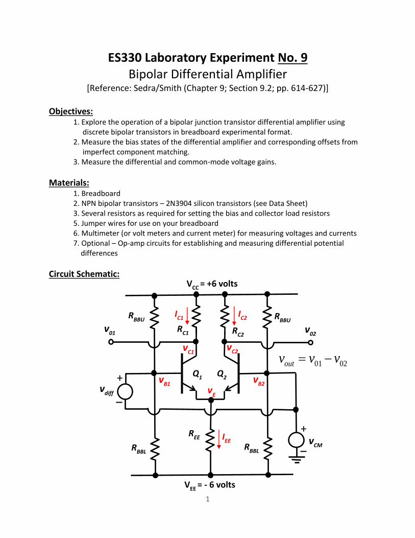
1 ES330 Laboratory Experiment No. 9 Bipolar Differential Amplifier [Reference: Sedra/Smith (Chapter 9; Section 9.2; pp. 614-627)] Objectives: 1. Explore the operation of a bipolar junction transistor differential amplifier using discrete bipolar transistors in breadboard experimental format. 2. Measure the bias states of the differential amplifier and corresponding offsets from imperfect component matching. 3. Measure the differential and common-mode voltage gains. Materials: 1. Breadboard 2. NPN bipolar transistors – 2N3904 silicon transistors (see Data Sheet) 3. Several resistors as required for setting the bias and collector load resistors 5. Jumper wires for use on your breadboard 6. Multimeter (or volt meters and current meter) for measuring voltages and currents 7. Optional – Op-amp circuits for establishing and measuring differential potential differences Circuit Schematic: V CC = +6 volts R C2 R C1 Q 1 Q 2 R EE v CM + + v diff v 01 v 02 V EE = - 6 volts R BBU R BBU R BBL R BBL 01 02 out v v v v C2 v C1 v B2 v B1 v E I C2 I C1 I EE
[Reference: Sedra/Smith (Chapter 9; Section 9.2; pp. 614-627)]
Objectives: 1. Explore the operation of a bipolar junction transistor differential amplifier using discrete bipolar transistors in breadboard experimental format. 2. Measure the bias states of the differential amplifier and corresponding offsets from imperfect component matching. 3. Measure the differential and common-mode voltage gains.
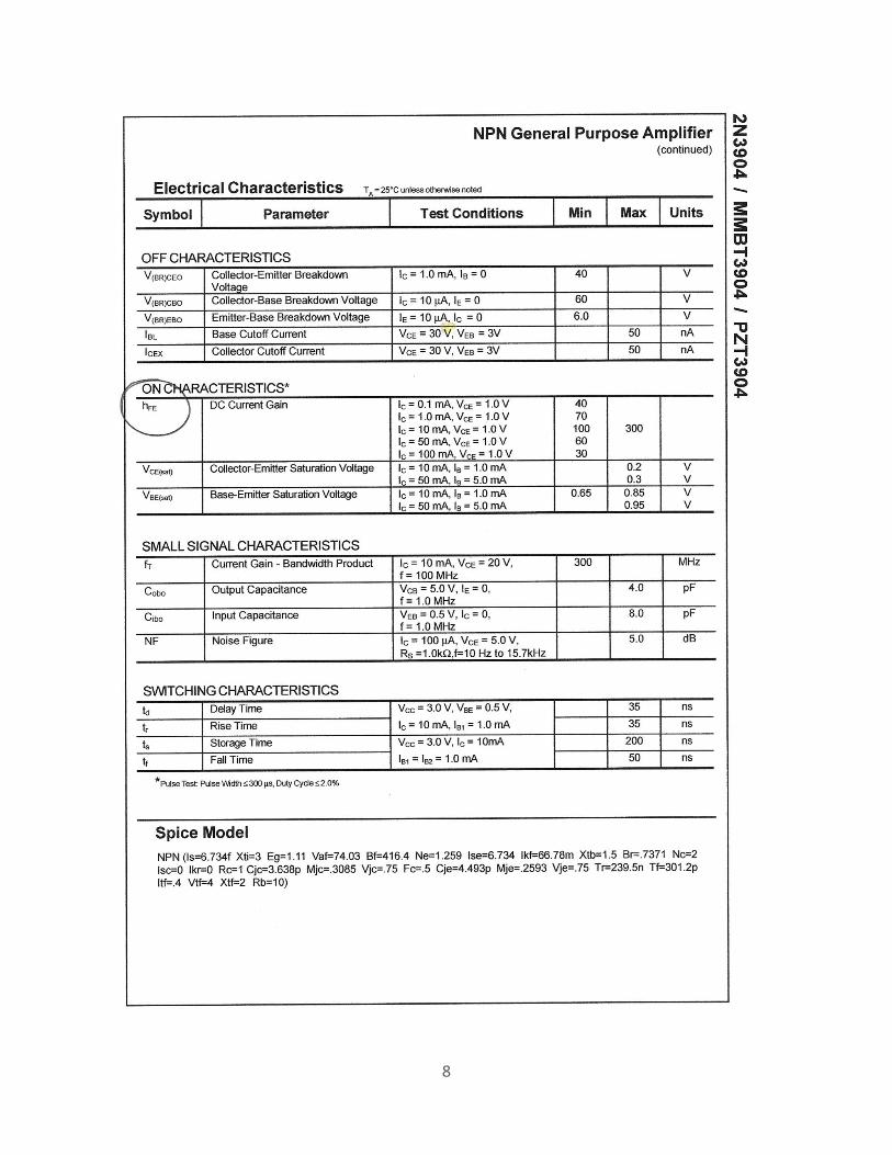
Materials: 1. Breadboard 2. NPN bipolar transistors – 2N3904 silicon transistors (see Data Sheet) 3. Several resistors as required for setting the bias and collector load resistors 5. Jumper wires for use on your breadboard 6. Multimeter (or volt meters and current meter) for measuring voltages and currents
7. Optional – Op-amp circuits for establishing and measuring differential potential differences
Circuit Schematic:
VCC
= +6 volts
RC2
RC1
Q1 Q
2
REE
v
CM
+
+
vdiff
v01
v02
VEE
= - 6 volts
RBBU
RBBU
RBBL
RBBL
01 02outv v v v
C2 v
C1
vB2
vB1
vE
IC2
IC1
IEE
2
Circuit Components: The parameters of the circuit are listed in the table below.
Component Value
Tail Current Resistor REE 5,300
Base resistors RBBU 10,000 (both matched if possible)
Base resistors RBBL 10,000 (both matched if possible)
NPN transistors 2N3904 (or an equivalent substitute as may be provided)
Collector resistors RC1 and RC2 6000 (both matched if possible)
VCC + 6 volts (nominal)
VEE - 6 volts (nominal)
This table lists component values needed for the differential amplifier circuit.
Parameter values for the 2N3904 bipolar transistor are provided in the 2N3904 Data Sheet in the appendix at the end of this document. Coupling capacitors are not included in the circuit schematic, however, they may be needed to keep whatever measurement probes connected to input terminals or output terminals from disturbing the DC potentials during your measurements.
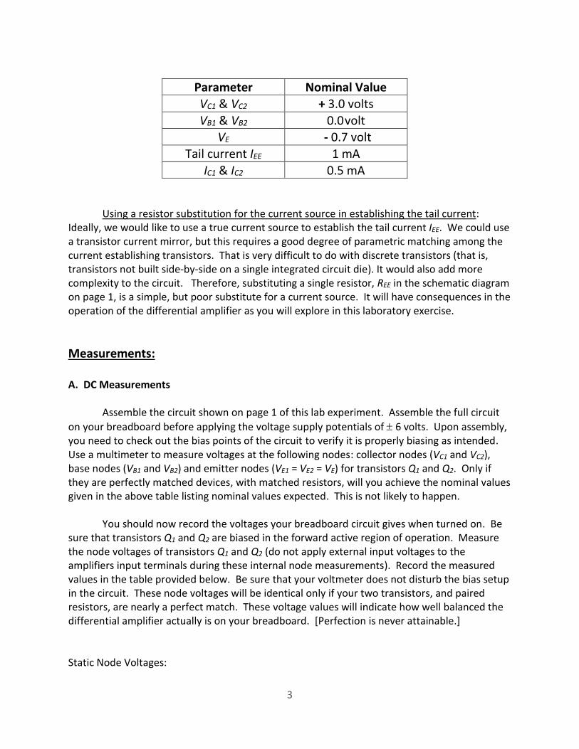
Selecting Bias Currents and Resistor Values: The quiescent bias points for transistors Q1 and Q2 are IC = 0.5 mA and VCE = 3.7 volts, with zero applied input voltages (i.e., Vdiff and VCM are nominally zero volts). Thus, the tail current will be IC1 + IC2 = IEE = 1 mA. Thus, we would expect the emitter node voltage VE to be
nominally - 0.7 volt (assumes the emitter-base voltages of both transistors to be VBE 0.7 volt). Under this assumption we expect base node voltages, VB1 and VB2, to be nominally at zero volts. With IC1 and IC2 equal to 0.5 mA, then let us choose approximately 3 volts to fall across the collector resistors (RC1 = RC2). To set the base node voltages close to zero volts the base voltage divider resistors RBBU and RBBL must be the same value (that assumes + 6 volts and – 6 volts for the voltage supplies).
For simplicity let us choose both resistors to be 10,000 ohms. (RBBU = RBBL = 10 k) You may
want to measure several 10 k resistors to select two resistors that have the best match, or
you can use a variable potentiometer in series with one of the 10 k resistors. Table summarizing design node voltages and currents:
3
Parameter Nominal Value VC1 & VC2 + 3.0 volts
VB1 & VB2 0.0 volt VE - 0.7 volt
Tail current IEE 1 mA
IC1 & IC2 0.5 mA Using a resistor substitution for the current source in establishing the tail current: Ideally, we would like to use a true current source to establish the tail current IEE. We could use a transistor current mirror, but this requires a good degree of parametric matching among the current establishing transistors. That is very difficult to do with discrete transistors (that is, transistors not built side-by-side on a single integrated circuit die). It would also add more complexity to the circuit. Therefore, substituting a single resistor, REE in the schematic diagram on page 1, is a simple, but poor substitute for a current source. It will have consequences in the operation of the differential amplifier as you will explore in this laboratory exercise.
Measurements: A. DC Measurements Assemble the circuit shown on page 1 of this lab experiment. Assemble the full circuit
on your breadboard before applying the voltage supply potentials of 6 volts. Upon assembly, you need to check out the bias points of the circuit to verify it is properly biasing as intended. Use a multimeter to measure voltages at the following nodes: collector nodes (VC1 and VC2), base nodes (VB1 and VB2) and emitter nodes (VE1 = VE2 = VE) for transistors Q1 and Q2. Only if they are perfectly matched devices, with matched resistors, will you achieve the nominal values given in the above table listing nominal values expected. This is not likely to happen. You should now record the voltages your breadboard circuit gives when turned on. Be sure that transistors Q1 and Q2 are biased in the forward active region of operation. Measure the node voltages of transistors Q1 and Q2 (do not apply external input voltages to the amplifiers input terminals during these internal node measurements). Record the measured values in the table provided below. Be sure that your voltmeter does not disturb the bias setup in the circuit. These node voltages will be identical only if your two transistors, and paired resistors, are nearly a perfect match. These voltage values will indicate how well balanced the differential amplifier actually is on your breadboard. [Perfection is never attainable.] Static Node Voltages:
4
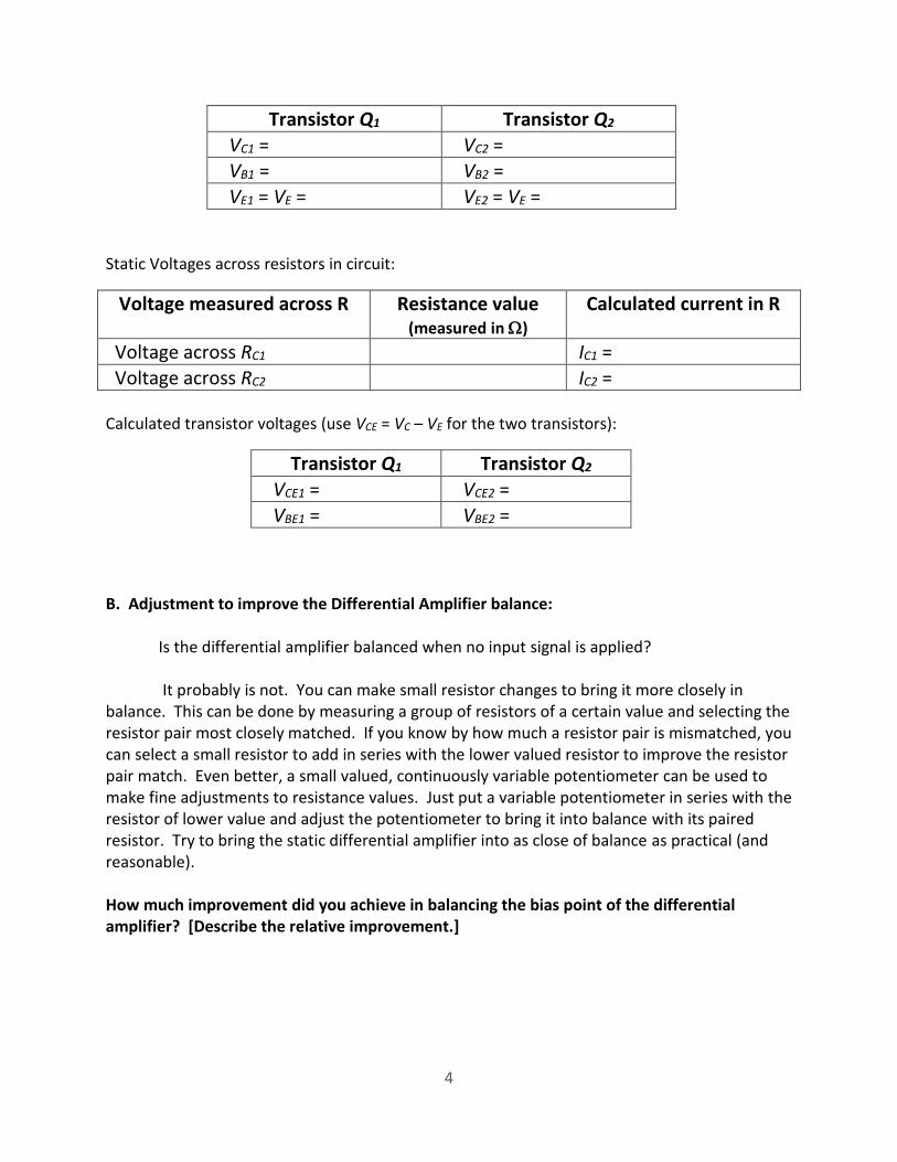
Transistor Q1 Transistor Q2
VC1 = VC2 = VB1 = VB2 =
VE1 = VE = VE2 = VE = Static Voltages across resistors in circuit:
Voltage measured across R Resistance value (measured in )
Calculated current in R
Voltage across RC1 IC1 =
Voltage across RC2 IC2 = Calculated transistor voltages (use VCE = VC – VE for the two transistors):
Transistor Q1 Transistor Q2
VCE1 = VCE2 =
VBE1 = VBE2 = B. Adjustment to improve the Differential Amplifier balance: Is the differential amplifier balanced when no input signal is applied? It probably is not. You can make small resistor changes to bring it more closely in balance. This can be done by measuring a group of resistors of a certain value and selecting the resistor pair most closely matched. If you know by how much a resistor pair is mismatched, you can select a small resistor to add in series with the lower valued resistor to improve the resistor pair match. Even better, a small valued, continuously variable potentiometer can be used to make fine adjustments to resistance values. Just put a variable potentiometer in series with the resistor of lower value and adjust the potentiometer to bring it into balance with its paired resistor. Try to bring the static differential amplifier into as close of balance as practical (and reasonable). How much improvement did you achieve in balancing the bias point of the differential amplifier? [Describe the relative improvement.]
5
Explain what you did to improve the bias point balance (with zero external applied input to the amplifier) of the differential stage. C. Output offset voltage error |VOS| with zero volt applied input voltage. [Reference: Section 9.4.2 starting with page 640 in Sedra & Smith] Assuming you have done your best (meaning within a reasonable amount of effort and time), now we want to determine the offset voltage error for an applied zero-volt differential input. In a differential amplifier you would like the differential output voltage to be zero volts when the applied input differential voltage is zero volts. If the differential output is not zero volts, then this is an offset error in the differential voltage gain of the differential amplifier. To test this parameter, DC connect both input nodes together (that is, short them together with a floating potential) and measure the differential output (if perfectly balanced it should give a differential output voltage error of zero volts). What reading did you get for this test? |VOS| = ________________________ Comment on how one might reduce the value of |VOS|.
6
D. AC Measurements Once the DC bias point of the differential amplifier is reasonably good, connect an AC signal generator (or function generator) differentially to the input to produce an AC voltage
gain from the amplifier. NOTE: to avoid upsetting the DC biasing, you will want to use 47 F capacitors as coupling capacitors to block any DC bias from the signal generator or function generator (just as were used the first two lab experiments). Be sure to limit the amplitude applied at the input to avoid overdriving the differential stage or saturating its output signal swing. You could also use single-ended measurements to AC characterize the differential gain of the amplifier. Be sure in that case to account for input signal division between the pair of inputs on the differential amplifier.
What differential voltage gain Ad did you measure? [See pages 623 and 624 in Sedra & Smith if you need further discussion.] Input signal level = ___________________ Output signal level = ___________________ Differential gain Ad = __________
Conclusions:
What have you learned from this laboratory experiment? Summarize your primary findings below. Write a summary describing what you gained (no pun intended) from doing this experiment.


![ES330 Laboratory Experiment No. 1 NPN Common-Emitter …ES330 Laboratory Experiment No. 1 NPN Common-Emitter Amplifier [Reference: Section 7.5.2 of Sedra & Smith (pp. 470-471)] ...](https://static.documents.pub/doc/80x56/5e4e56cb0406fa15a46f4ff6/es330-laboratory-experiment-no-1-npn-common-emitter-es330-laboratory-experiment.jpg)


![ES330 Laboratory Experiment No. 1 NPN Common … ES330 Laboratory Experiment No. 1 NPN Common-Emitter Amplifier [Reference: Section 7.5.2 of Sedra & Smith (pp. 470-471)] Objectives:](https://static.documents.pub/doc/80x56/5aded8fe7f8b9afd1a8be8ac/es330-laboratory-experiment-no-1-npn-common-es330-laboratory-experiment-no.jpg)

