This is information on a product in full production. July 2014 DocID025281 Rev 1 1/23 HDMI2C1-6C1 ESD protection and signal booster for HDMI™ source control stage interface Datasheet − production data Features • HDMI 1.3 and 1.4 compliant: from -40 to 85 °C • 8 kV contact ESD protection on connector side • Supports direct connection to low-voltage HDMI ASIC and/or CEC driver (down to 1.8 V) • High integration level in 1 package • DDC (I2C) link protection, bi-directional signal conditioning circuit, and dynamic pull-up • CEC bus protection, bi-directional level-shifter, backdrive protection, and independent structure from main power supply • HEAC link protection and line matching • HPD pull down and signal conditioning • Short-circuit protection on 5 V output • Over temperature protection • Proposed in QFN 18 leads 500 μm pitch Benefits • Speed-up hardware design and certification of HDMI application • Pin map sequence compliant with HDMI connector type A • Minimal PCB footprint in consumer area • Protection of ultra-sensitive HDMI ASICs • Ultra low power consumption in stand-by mode • Wake-up from stand-by through CEC bus • Improved HDMI interface ruggedness and user experience • Long and/or poor quality cable support Complies with the following standards • HDMI 1.3 and 1.4 version • IEC 61000-4-2 level 4 • JESD22-A114D level 2 Description The HDMI2C1-6C1 is an integrated ESD protection and signal conditioning device for control links of HDMI transmitters (Source). The HDMI2C1-6C1 is a simple solution that provides HDMI designers with an easy and fast way to reach full compliancy with the stringent HDMI CTS on a wide temperature range. Applications • Consumer and computer electronics HDMI Source device such as: – HD set-top boxes – DVD and Blu-Ray Disk systems – Notebook – PC graphic cards TM: HDMI: the HDMI logo and high definition multimedia interface are trademarks or registered trademarks of HDMI Licensing LLC. QFN_18L 3.5 x 3.5 pitch 0.5 mm www.st.com
Transcript
This is information on a product in full production.
July 2014 DocID025281 Rev 1 1/23
HDMI2C1-6C1
ESD protection and signal booster for HDMI™ source control stage interface
Datasheet − production data
Features
• HDMI 1.3 and 1.4 compliant: from -40 to 85 °C
• 8 kV contact ESD protection on connector side
• Supports direct connection to low-voltage HDMI ASIC and/or CEC driver (down to 1.8 V)
• High integration level in 1 package
• DDC (I2C) link protection, bi-directional signal conditioning circuit, and dynamic pull-up
• CEC bus protection, bi-directional level-shifter, backdrive protection, and independent structure from main power supply
• HEAC link protection and line matching
• HPD pull down and signal conditioning
• Short-circuit protection on 5 V output
• Over temperature protection
• Proposed in QFN 18 leads 500 µm pitch
Benefits
• Speed-up hardware design and certification of HDMI application
• Pin map sequence compliant with HDMI connector type A
• Minimal PCB footprint in consumer area
• Protection of ultra-sensitive HDMI ASICs
• Ultra low power consumption in stand-by mode
• Wake-up from stand-by through CEC bus
• Improved HDMI interface ruggedness and user experience
• Long and/or poor quality cable support
Complies with the following standards
• HDMI 1.3 and 1.4 version
• IEC 61000-4-2 level 4
• JESD22-A114D level 2
Description
The HDMI2C1-6C1 is an integrated ESD protection and signal conditioning device for control links of HDMI transmitters (Source).
The HDMI2C1-6C1 is a simple solution that provides HDMI designers with an easy and fast way to reach full compliancy with the stringent HDMI CTS on a wide temperature range.
Applications
• Consumer and computer electronics HDMI Source device such as:
– HD set-top boxes
– DVD and Blu-Ray Disk systems
– Notebook
– PC graphic cards
TM: HDMI: the HDMI logo and high definition multimedia interface are trademarks or registered trademarks of HDMI Licensing LLC.
The HDMI2C1-6C1 is a fully integrated ESD protection and signal conditioning device for control stage of HDMI™ transmitters (Source).
The component offers a bidirectional buffer, integrating signal conditioning and dynamic pull-up on DDC bus for maximum system robustness and signal integrity. A bidirectional CEC block is integrated, able to wake-up the application from stand-by mode (all power supply off, except the CEC power supply). The +5 V supplied to the cable is protected against accidental surge current and short circuit. All these features are provided in a single 18 leads QFN package featuring natural PCB routing and saving space on the board. The HEAC (HDMI Ethernet and Audio return Channels) function is supported, making the component fully compliant with HDMI™ 1.4 version.
The HDMI2C1-6C1 is a simple solution that provides HDMI™ designers with an easy and fast way to reach full compliancy with the stringent HDMI™ CTS on a wide temperature range. STMicroelectronics proposes also a large range of High Speed ESD protections and common mode filter (ECMF™ series) dedicated to the TMDS lanes giving the flexibility to the designer to filter and protect these high speed video links against ESD strikes and EMC issues. Last, a fully integrated version HDMI2C1-14HD exists, grouping equivalent control stage functional blocks, plus the high speed ESD protection for TMDS lanes.
Figure 1. Pin out, top view
HDP_IC
HD
P
UT
ILIT
Y
SDA_IC
CEC_IC
SCL_IC
FAULT 1
5
6 9
SCL
GND
CEC
VDD_CEC
SDA
GND
VD
D_
5V
5V
_O
UT
VD
D_
IC
VD
D_
CE
C_
IC
HE
AC
-
HE
AC
+
10
14
1518
Application information HDMI2C1-6C1
4/23 DocID025281 Rev 1
2 Application information
2.1 CEC line description
The CEC bus is described in the HDMI standard as the consumer electronics control. It provides control functions between all the various audiovisual equipment chained in the user's environment.
The CEC block integrated in the HDMI2C1-6C1 implements a level shifter, shifting the cable CEC line from +3.3 V CEC voltage (VDD_CEC) down to the ASIC power supply voltage (VDD_IC) that can be as low as 1.8 V. The Figure 2 shows the functional diagram of the integrated CEC block.
Figure 2. CEC link functional block diagram
In case of no activity on the CEC bus, or if the CEC driver is off (VDD_CEC = 0), the output CEC pin is put in high impedance mode (open circuit) protecting the circuitry and the application against hazardous backdrive.
The Figure 3 illustrates the normal operating mode of the CEC functional block when either the IC from the source or the sink drives the communication.
Figure 3. CEC simplified
CEC_IC
VDD_CEC_IC
CEC
VDD_CECVDD_CEC_IC
VDD_CEC
CEC
driver
UVLO
Ctrlcircuit
Enable
1
3
5
7
9
1112
1314
1516
1718
19
2
4
6
8
10
HDMI
connector
decoupling
de
co
up
lin
g
capacitance
ca
pa
cit
an
ce
RP
U_
CE
C_
IC
HB
M
IEC
61
00
0-4
-2
RP
U_
CE
C_
BU
SA
nti
ba
ck
dri
ve
dio
de
Cab
le s
ide
AS
IC s
ide
VDD_CEC_IC
CEC_IC
VDD_CEC
CEC
VTdown_CEC
VTup_CEC
VHYST_CEC
VDD_CEC_IC
CEC_IC
VDD_CEC
CEC
VIL_CEC_IC
VIH_CEC_IC
Block in highimpedance Level shifting
Source IC drivesSink drives through HDMI cable
Block in highimpedance Block in high
impedance Level shiftingBlock in highimpedance
t
t
t
t10%
90%
tFALL_CEC tRISE_CEC
DocID025281 Rev 1 5/23
HDMI2C1-6C1 Application information
23
In case the application is set in stand-by mode, the +5 V main supply of the application is generally powered off in order to reduce as much as possible the global power consumption. The CEC driver can be the only device still working in low power mode, allowing a wake up of the whole application through the CEC line. When the main power supply +5 V is switched off, and if the CEC bus is still active (VDD_CEC power in on state), the HDMI2C1-6C1 keeps the CEC bus working properly while all other outputs of the component are put in high impedance mode.
The CEC output (cable side) integrates a protection against ESD which is compliant with IEC61000-4-2 standard, level 4 (8kV contact).
2.2 DDC bus description
The DDC bus is described in the HDMI™ standards as the Display Data Channel. The topology corresponds to an I2C bus that must be compliant with the I2C bus specification version 2.1 (January 2000). The DDC bus is made of 2 lines: data line (SDA) and clock line (SCL). It is used to create a point to point communication link from the Source to the Sink. EEDID and HDCP protocols are especially flowing through this link, making this I2C communication channel a key element in the HDMI™ application.
The DDC block integrated in the HDMI2C1-6C1 allows a bidirectional communication between the cable and the ASIC. It is fully compliant with the HDMI™ 1.4 standard and its CTS, and with the I2C bus specification version 2.1. It is shifting the 5 V voltage from the cable (V5V_OUT) down to the ASIC voltage level (VDD_IC) that can be as low as 1.8 V. The Figure 4 shows the functional diagram of the DDC block integrated in the HDMI2C1-6C1 device.
Figure 4. The DDC functional block diagram (SCL and SDA lines)
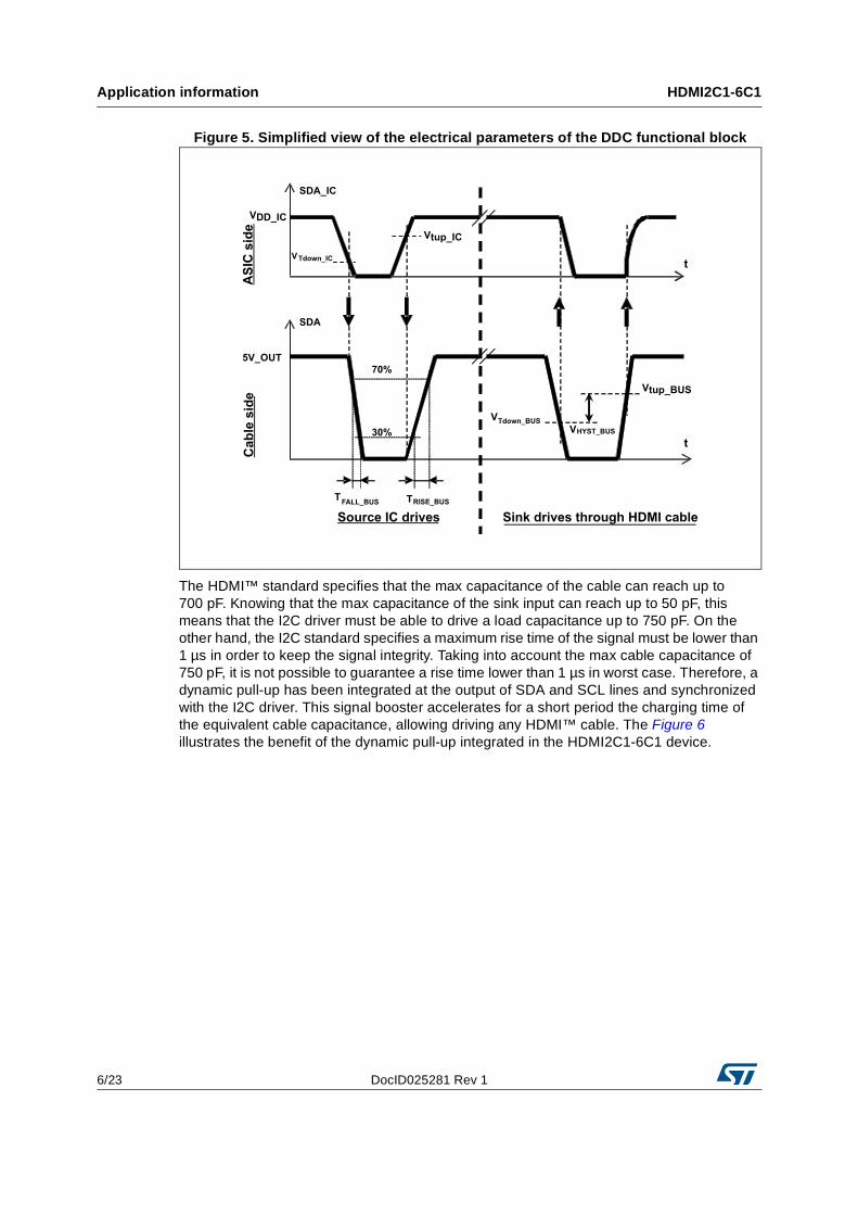
The Figure 5 illustrates the electrical parameter of the DDC block specified in Table 8.
SCL_IC
SDA_IC
VDD_IC
reshapingcircuit
VDD_5V
5V_OUT
SCL
SDA
VDD_IC
HDMI
ASIC
+5V
UVLO
VDD_5V
5V_OUT
Enable
Drive HDMI
connector
decouplingcapacitance
1
3
5
7
9
11
13
15
17
19
12
14
16
18
2
4
6
8
10
RP
U_
AS
IC
HB
M
RP
U_
BU
S
IEC
61
00
0-4
-2
dy
na
mic
pu
ll -
up
Application information HDMI2C1-6C1
6/23 DocID025281 Rev 1
Figure 5. Simplified view of the electrical parameters of the DDC functional block
The HDMI™ standard specifies that the max capacitance of the cable can reach up to 700 pF. Knowing that the max capacitance of the sink input can reach up to 50 pF, this means that the I2C driver must be able to drive a load capacitance up to 750 pF. On the other hand, the I2C standard specifies a maximum rise time of the signal must be lower than 1 µs in order to keep the signal integrity. Taking into account the max cable capacitance of 750 pF, it is not possible to guarantee a rise time lower than 1 µs in worst case. Therefore, a dynamic pull-up has been integrated at the output of SDA and SCL lines and synchronized with the I2C driver. This signal booster accelerates for a short period the charging time of the equivalent cable capacitance, allowing driving any HDMI™ cable. The Figure 6 illustrates the benefit of the dynamic pull-up integrated in the HDMI2C1-6C1 device.
5V_OUT
SDA
VDD_IC
SDA_IC
VTdown_IC
TRISE_BUS
Vtup_IC
70%
30%
VTdown_BUS
Vtup_BUS
VHYST_BUS
Source IC drives
AS
IC s
ide
Ca
ble
sid
e
Sink drives through HDMI cable
TFALL_BUS
t
t
DocID025281 Rev 1 7/23
HDMI2C1-6C1 Application information
23
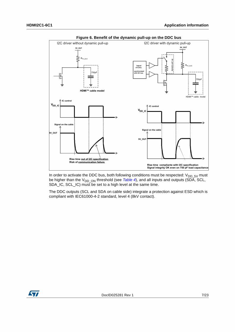
Figure 6. Benefit of the dynamic pull-up on the DDC bus
In order to activate the DDC bus, both following conditions must be respected: VDD_5V must be higher than the VDD_ON threshold (see Table 4), and all inputs and outputs (SDA, SCL, SDA_IC, SCL_IC) must be set to a high level at the same time.
The DDC outputs (SCL and SDA on cable side) integrate a protection against ESD which is compliant with IEC61000-4-2 standard, level 4 (8kV contact).
RPU_BUS
5V_OUT
750pF
dyn
am
ic p
ull -
up
HDMI™ cable model
Signal on the cable
IC control
5V_OUT
5V_OUT
V
V
DD_IC
DD_IC
IC control
Signal on the cable
Rise time out of I2C specification
Risk of communication failureRise time compliante with I2C specificationSignal integrity OK even on 750 pF load capacitance
I2C driver without dynamic pull-up I2C driver with dynamic pull-up
RPU_BUS
5V_OUT
HDMI™ cable model
750pF
logical
circuitry
synchronized
with I2C bus
Application information HDMI2C1-6C1
8/23 DocID025281 Rev 1
2.3 HEAC link and HPD line description
The HDMI2C1-6C1 proposes a unique solution in order to manage and protect both the HEAC and the HPD links. The Figure 7 shows an overview of the function diagram of the integrated block.
This block simplifies the design and the PCB layout of the HPD and HEAC functions. Simply connect the 2 pins from the HDMI connector to one side of the device, and then use the 3 dedicated outputs on the other side of the device to manage separately the HPD and the HEAC links.
Both HPD and Utility inputs (cable side) integrate a protection against ESD which is compliant with IEC61000-4-2 standard, level 4 (8 kV contact).
2.3.1 HPD line description
The HPD line is described in the HDMI standard as the hot plug detect function. This line is used by the source device in order to detect if a sink device is connected through an HDMI cable.
The integrated HPD block is pulling down the line via a current source. When the input voltage is detected to be higher than a threshold level, the signal is converted into a high state level on the ASIC side, at the voltage level of the ASIC power supply VDD_IC. Otherwise, CEC_IC pin remains in low state.
The electrical parameters relevant to the HPD block and specified by theTable 7 are illustrated in the Figure 8.
HPD
HPD_IC
Utility
HDMI
ASIC
or
IC
VDD_IC
matching
Utility / HEAC+
HPD / HEAC-
HEAC+
HEAC -
VDD_IC
HDMI
connector
1
3
5
7
9
11
13
15
17
19
12
14
16
18
2
4
6
8
10
IEC
61000-4
-2IE
C61000-4
-2
HB
M
deco
up
lin
gcap
acit
an
ce
DocID025281 Rev 1 9/23
HDMI2C1-6C1 Application information
23
Figure 8. Simplified view of the electrical parameters of the HPD block
2.3.2 HEAC link
The HEAC link is described in the HDMI 1.4 standards as the HDMI ethernet and audio return channel. It corresponds physically to one differential wired pair made of the Utility line and the HPD line. Two signals are transmitted through this link.
The first signal corresponds to the HDMI ethernet channel (HEC). The signal is transmitted in differential mode (bidirectional) through the HEAC link. It is specified by the 100Base-TX IEEE 802.3 standard (fast ethernet 100Mbps over twisted pair). Therefore, the HEC integrates an ethernet link into the video cable, enabling IP-based applications over the HDMI cable.
The second signal corresponds to the audio return channel (ARC). The signal is transmitted either in common mode (unidirectional, from sink to source) through the HEAC link. It is specified by the IEC 60958-1 standard. The ARC function integrates an upstream audio capability, simplifying the cabling of the audiovisual equipment. It is no more necessary to use a coaxial cable from TV to audio amplifier.
The HDMI2C1-6C1 helps the designer to implement this high added value HEAC function in the application, protecting the link against the ESD with no disturbance of the signal. It provides 2 distinct outputs HEAC+ and HEAC in order to ease as much as possible the PCB layout.
2.4 +5V protection and fault line
The +5 V power supply that the source device has to provide to the HDMI cable is described by the HDMI 1.4 standard. It must be protected against accidental short circuit that could occur on the cable side.
The HDMI2C1-6C1 device embeds a low drop current limiter. If an overcurrent is detected, the HDMI2C1-6C1 limits the current through the +5V power supply. If the current is too high (short circuit), the device opens the +5V.
Furthermore, the HDMI2C1-6C1 device embeds also an over temperature protection (OTP). If the internal temperature of the device is reaching a too high value, the +5V supply is opened in order to protect the application.
HPD_IC signal
Signal on HPD link
VIL_HPD
VIH_HPD
5V
Application information HDMI2C1-6C1
10/23 DocID025281 Rev 1
In case either the current limiter or the OTP is triggered, a logic signal is sent over the fault line in order to inform the HDMI™ ASIC that an abnormal situation has been detected (option).
An under voltage lockout (UVLO) is also integrated in the block. It checks the main +5 V power supply state, and enable the +5V_OUT only if the main power supply has reach a minimal value VDD_5V_ON.
The Figure 9 shows the functional diagram of the current limiter block.
Figure 9. +5V functional block diagram
To summarize, the short circuit protection and the over temperature protection features provide a high robustness level of the application. On top of this, the fault line can be used in order to improve the user experience.
The 5V_OUT pin integrates a protection against ESD which is compliant with IEC61000-4-2 standard, level 4 (8 kV contact). The decoupling capacitance is mandatory, according to the power management state of the art.
VDD_5V +5V_OUT
Ctrl
5V
FAULT
HDMI
ASIC
or
IC
VDD_IC
UVLO
Current
sensor
OTP
RPU_FAULT
HDMI
connector
Low drop current limiter
de
co
up
lin
g
de
co
up
lin
g
ca
pa
cit
an
ce
ca
pa
cit
an
ce
HB
MH
BM
IEC
61000-4
-2
1
3
5
7
9
11
13
15
17
19
12
14
16
18
2
4
6
8
10
DocID025281 Rev 1 11/23
HDMI2C1-6C1 Application information
23
2.5 Application block diagram
The Figure 10 shows a typical application block diagram proposal implementing all the possible options. The diagram shows that the CEC driver can be totally independent from the HDMI™ ASIC. In this way, even if the +5 V power supply and/or if the HDMI™ ASIC is sleeping in stand-by mode, the CEC bus is still active in low power mode. In this way, the designer has then the tools to optimize the power consumption of the global application in stand-by mode, and at the same time, has the possibility to implement a smart wake-up through the CEC bus enhancing the final user experience.
Figure 10. Application block diagram
Note: SCL_IC, SDA_IC, and CEC_IC have to be driven with an ASIC working with open drain outputs.
Table 1. Block diagrams references
Ref. Typical values Comment
R1 27 kΩ Pull-up resistance on CEC bus, specified by the HDMI standard
R2, R3 1.8 kΩ Pull-up resistances on DDC bus, specified by the HDMI standard
R4, R5 10 kΩ Pull-up resistance on DDC bus, ASIC side, value selected to be compliant with I2C levels
R6 270 kΩ to 1 ΜΩ Pull-up resistance on CEC line, ASIC side
R7 10 kΩ Pull-up resistance on FAULT line (option)
D1 BAT54Small schottky diode blocking backdrive current flowing toward the VDD_CEC supply
C1 to C5 100 nF Decoupling capacitance on power supplies
CECdriver
+5V
SCL_IC
SDA_IC SDA
SCL
CEC bus
VDD_CEC_IC
VDD_IC
VDD_IC
VDD_CEC
VDD_5V
VDD_IC
FAULT
HPD_IC
VDD_CEC_IC
CEC_IC
5V_OUT
HPD
SDA
SCL
CEC
VDD_CEC
Utility
VDD_ICHPD
DDC data
HPD / HEAC-
Utility / HEAC+HEAC-
HEAC+
over current
detect
HEAC-
HEAC+
HDMI2C1
HD
MIA
SIC
HD
MI
co
nn
ec
tor
- 6C1
+5V power
C4C3R2R3
C2
R1
D1
C1C5R6
R4
R5
DDC clock
R7
GND
Application information HDMI2C1-6C1
12/23 DocID025281 Rev 1
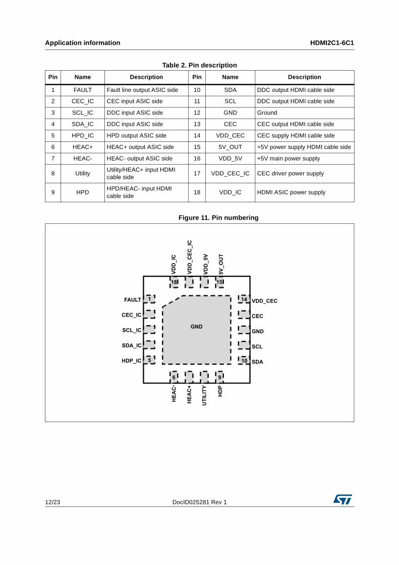
Figure 11. Pin numbering
Table 2. Pin description
Pin Name Description Pin Name Description
1 FAULT Fault line output ASIC side 10 SDA DDC output HDMI cable side
2 CEC_IC CEC input ASIC side 11 SCL DDC output HDMI cable side
3 SCL_IC DDC input ASIC side 12 GND Ground
4 SDA_IC DDC input ASIC side 13 CEC CEC output HDMI cable side
5 HPD_IC HPD output ASIC side 14 VDD_CEC CEC supply HDMI cable side
6 HEAC+ HEAC+ output ASIC side 15 5V_OUT +5V power supply HDMI cable side
7 HEAC- HEAC- output ASIC side 16 VDD_5V +5V main power supply
8 UtilityUtility/HEAC+ input HDMI cable side
17 VDD_CEC_IC CEC driver power supply
9 HPDHPD/HEAC- input HDMI cable side
18 VDD_IC HDMI ASIC power supply
HDP_IC
HD
P
UT
ILIT
Y
SDA_IC
CEC_IC
SCL_IC
FAULT 1
5
6 9
SCL
GND
CEC
VDD_CEC
SDA
GND
VD
D_
5V
5V
_O
UT
VD
D_
IC
VD
D_
CE
C_
IC
HE
AC
-
HE
AC
+
10
14
1518
DocID025281 Rev 1 13/23
HDMI2C1-6C1 Electrical characteristics
23
3 Electrical characteristics
Table 3. Absolute maximum ratings (limiting values)
Symbol Parameter Test conditions Value Unit
Vpp_BUSESD discharge on HDMI BUS side (pin 8 to 16), IEC 61000-4-2 level 4
2. Maximum load capacitance allowed on I2C entire link (cable + connector) is 750 pF in HDMI 1.4 specification.
3. Two pull-up resistors in parallel (sink 47 kΩ + source 2 kΩ).
4. Maximum capacitance allowed at connector output is 50 pF in HDMI 1.4 specification
Electrical characteristics HDMI2C1-6C1
16/23 DocID025281 Rev 1
Figure 12. CEC typical waveforms (IC to cable communication)
Figure 13. CEC typical waveforms (cable to IC communication)
Figure 14. DDC typical waveforms (IC to cable communication)
C3 = 500 mV/div
rise = 459.98 µs
fall = 2.34 µs
C2 = 1.00 V/div
200 µs/div
top = 3.29 V
base = -12.0 mV
C3 = 500 mV/div
rise = 120.02 µs
fall = 966.6 ns
C2 = 1.00 V/div
200 µs/div
top = 1.80 V
base = 31.0 mV
C3 = 500 mV/div
fall = 78.07 ns
C2 = 1.00 V/div
2 µs/div
top = 4.99 V
base = 90.0 mV
rise = 454.8 ns
DocID025281 Rev 1 17/23
HDMI2C1-6C1 Electrical characteristics
23
Figure 15. DDC typical waveforms (cable to IC communication)
Figure 16. HPD typical waveforms (timing)
Figure 17. HEAC single ended mode typical bandwidth
C3 = 500 mV/div
fall = 1.97 ns
C2 = 1.00 V/div
2 µs/div
top = 1.80 V
base = 17.8 mV
rise = 1.25 µs
C3 = 500 mV/div
fall = 9.47 ns
C2 = 1.00 V/div
1 µs/div
top = 1.80 V
base = -6.8 mV
rise = 37.83 ns
dB
100k 1M 10M 100M 1G 10G
-12
-11
-10
-9
-8
-7
-6
-5
-4
-3
-2
-1
0
HEAC+ HEAC-
F(Hz)
Package information HDMI2C1-6C1
18/23 DocID025281 Rev 1
4 Package information
• Epoxy meets UL94, V0
• Lead-free packages
In order to meet environmental requirements, ST offers these devices in different grades of ECOPACK® packages, depending on their level of environmental compliance. ECOPACK® specifications, grade definitions and product status are available at: www.st.com. ECOPACK® is an ST trademark.
Figure 18. QFN definitions
b
E2
e
L
D2
E
D
K
A
A1
DocID025281 Rev 1 19/23
HDMI2C1-6C1 Package information
23
Figure 19. QFN footprint recommendation (dimensions in mm)
Table 9. QFN dimension values
Ref
Dimensions
Millimeters Inches
Min. Typ. Max. Min. Typ. Max.
A 0.51 0.55 0.60 0.020 0.021 0.23
A1 0.00 0.02 0.05 0.00 0.00 0.001
b 0.18 0.25 0.30 0.007 0.009 0.011
D 3.50 0.137
D2 1.99 2.14 2.24 0.078 0.084 0.088
E 3.50 0.137
E2 1.99 2.14 2.24 0.078 0.084 0.088
e 0.50 0.019
L 0.30 0.40 0.50 0.011 0.015 0.019
K 0.20 0.007
0.300.50
0.20
2.20
2.2
0
3.60
3.6
0
0.50
0.5
0
Recommendation on PCB assembly HDMI2C1-6C1
20/23 DocID025281 Rev 1
5 Recommendation on PCB assembly
5.1 Stencil opening design
1. General recommendation on stencil opening design
a) Stencil opening dimensions: L (Length), W (Width), T (Thickness).
Figure 20. Stencil opening dimensions
b) General design rule
Stencil thickness (T) = 75 ~ 125 µm
2. Reference design
a) Stencil opening thickness: 100 µm
b) Stencil opening for leads: Opening to footprint ratio is 90%.
Figure 21. Recommended stencil window position
L
TW
Aspect Ratio WT----- 1.5≥=
Aspect AreaL W×
2T L W+( )---------------------------- 0.66≥=
0.300.50
0.20
2.20
2.2
0
3.60
3.6
0
0.50
0.5
0
13 µm
286 µm
300 µm
47
4 µ
m
50
0 µ
m
7 µm
300 µm
1.6 mm
1.6
mm
2.2 mm
2.2
mm
300 µm
Stencil window
Footprint
DocID025281 Rev 1 21/23
HDMI2C1-6C1 Recommendation on PCB assembly
23
5.2 Solder paste
1. Use halide-free flux, qualification ROL0 according to ANSI/J-STD-004.
2. “No clean” solder paste recommended.
3. Offers a high tack force to resist component displacement during PCB movement.
4. Use solder paste with fine particles: powder particle size 20-45 µm.
5.3 Placement
1. Manual positioning is not recommended.
2. It is recommended to use the lead recognition capabilities of the placement system, not the outline centering.
3. Standard tolerance of ± 0.05 mm is recommended.
4. 3.5 N placement force is recommended. Too much placement force can lead to squeezed out solder paste and cause solder joints to short. Too low placement force can lead to insufficient contact between package and solder paste that could cause open solder joints or badly centered packages.
5. To improve the package placement accuracy, a bottom side optical control should be performed with a high resolution tool.
6. For assembly, a perfect supporting of the PCB is recommended during solder paste printing, pick and place and reflow soldering by using optimized tools.
5.4 PCB design preference
1. To control the solder paste amount, closed vias are recommended instead of open vias.
2. The position of tracks and open vias in the solder area should be well balanced. Symmetrical layout is recommended, in case any tilt phenomena caused by asymmetrical solder paste amount due to the solder flow away.
5.5 Reflow profile
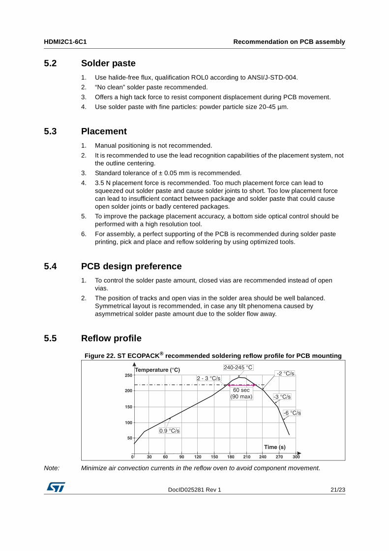
Figure 22. ST ECOPACK® recommended soldering reflow profile for PCB mounting
Note: Minimize air convection currents in the reflow oven to avoid component movement.
250
0
50
100
150
200
240210180150120906030 300270
-6 °C/s
240-245 °C
2 - 3 °C/s
Temperature (°C)-2 °C/s
-3 °C/s
Time (s)
0.9 °C/s
60 sec(90 max)
Ordering information HDMI2C1-6C1
22/23 DocID025281 Rev 1
6 Ordering information
Figure 23. Ordering information scheme
7 Revision history
Table 10. Ordering information
Order code Marking Package Weight Base qty Delivery mode
HDMI2C1-6C1 6HEAC QFN 22.3 mg 3,000 Tape and Reel
HDMI2C 1 - 6 C 1
HDMI and I2C compliant links
Number of protected links6 lines protected according to IEC 6100-4-2
VersionHD: Full speed of HDMI supported
Version
HDMI port type1: source ports
Table 11. Document revision history
Date Revision Changes
25-Jul-2014 1 Initial release
DocID025281 Rev 1 23/23
HDMI2C1-6C1
23
IMPORTANT NOTICE – PLEASE READ CAREFULLY
STMicroelectronics NV and its subsidiaries (“ST”) reserve the right to make changes, corrections, enhancements, modifications, and improvements to ST products and/or to this document at any time without notice. Purchasers should obtain the latest relevant information on ST products before placing orders. ST products are sold pursuant to ST’s terms and conditions of sale in place at the time of order acknowledgement.
Purchasers are solely responsible for the choice, selection, and use of ST products and ST assumes no liability for application assistance or the design of Purchasers’ products.
No license, express or implied, to any intellectual property right is granted by ST herein.
Resale of ST products with provisions different from the information set forth herein shall void any warranty granted by ST for such product.
ST and the ST logo are trademarks of ST. All other product or service names are the property of their respective owners.
Information in this document supersedes and replaces information previously supplied in any prior versions of this document.