Any opinions, findings, conclusions or recommendations expressed in this publication are those of the author(s) and do not necessarily reflect the views of the Office of Naval Research. NOTIONAL SYSTEM MODELS Technical Report Submitted to: The Office of Naval Research Contract Number: N0014-08-1-0080 Submitted by: Mike Andrus, Florida State University Matthew Bosworth, Florida State University Jonathan Crider, Purdue University Hamid Ouroua, University of Texas at Austin Enrico Santi, University of South Carolina Scott Sudhoff, Purdue University December, 2013 Approved for Public Release – Distribution Unlimited
Transcript
Any opinions, findings, conclusions or recommendations expressed in this publication are those of the author(s) and do not necessarily reflect the views of the Office of Naval Research.
NOTIONAL SYSTEM MODELS
Technical Report
Submitted to: The Office of Naval Research
Contract Number: N0014-08-1-0080
Submitted by: Mike Andrus, Florida State University
Matthew Bosworth, Florida State University Jonathan Crider, Purdue University
Hamid Ouroua, University of Texas at Austin Enrico Santi, University of South Carolina
Scott Sudhoff, Purdue University
December, 2013
Approved for Public Release – Distribution Unlimited
2000 Levy Avenue, Suite 140 | Tallahassee, FL 32310 | www.esrdc.com
MISSION STATEMENT The Electric Ship Research and Development Consortium brings together in a single entity the combined programs and resources of leading electric power research institutions to advance near- to mid-term electric ship concepts. The consortium is supported through a grant from the United States Office of Naval Research.
Fig. 5.1.1: Notional Power System. ............................................................................................... 7Fig. 5.1.2: Notional MVAC Zone. ................................................................................................. 8Fig. 5.1.3: Notional HFAC Zone. .................................................................................................. 8Fig. 5.1.4: Notional MVDC Zone. ................................................................................................. 9Fig. 5.3.1: Synchronous Generator Exciter Model. ..................................................................... 14Fig. 5.4.1: Droop Function of Speed Regulator without RTSC. .................................................. 17Fig. 5.4.2: Droop Function of Speed Regulator With RTSC. ...................................................... 18Fig. 5.4.3: Structure of the RTSC Consisting of Frequency Control and Phase Control. ........... 19Fig. 5.5.1: Generic Single-Shaft Gas Turbine Model [5.5.1]. ..................................................... 22Fig. 5.5.2: Generic Twin-Shaft Gas Turbine Model. ................................................................... 24Fig. 5.6.1: Synchronous Machine Fed Load Commutated Converter. ........................................ 26Fig. 5.6.2: DC Generator Circuit Breaker Control. ...................................................................... 32Fig. 5.7.1: DC Generator Exciter. ................................................................................................ 33Fig. 5.8.1: DC Propulsion Drive. ................................................................................................. 35Fig. 5.8.2: DC Link. ..................................................................................................................... 38Fig. 5.8.3: Resistor Brake Control. .............................................................................................. 39Fig. 5.8.4: Propulsion Control. ..................................................................................................... 40Fig. 5.8.5: DC Propulsion Supervisory Control. .......................................................................... 41Fig. 5.9.1: Propulsion Drive Transformer Rectifier. .................................................................... 42Fig. 5.10.1: DC Generic Pulsed Load. ......................................................................................... 46Fig. 5.10.2: AC Generic Pulsed Load. ......................................................................................... 46Fig. 5.10.3: GPL Supervisory Control. ........................................................................................ 50Fig. 5.14.1: Transformer Q-axis Equivalent Circuit. ................................................................... 58Fig. 5.14.2: Transformer D-axis Equivalent Circuit. ................................................................... 59Fig. 5.15.1: Zonal Active Rectifier. ............................................................................................. 61
iii
Fig. 5.15.2: Zonal Active Rectifier Supervisory Control. ............................................................ 62Fig. 5.15.3: Zonal Active Rectifier Output Voltage. ................................................................... 62Fig. 5.16.1: Zonal DC Load. ........................................................................................................ 64Fig. 5.16.2: Zonal DC Load Supervisory Control. ...................................................................... 65Fig. 5.18.1: Zonal AC Load. ........................................................................................................ 66Fig. 5.18.2: Zonal AC Load Supervisory Control. ...................................................................... 68Fig. 5.19.1: DC-DC Converter Topology. ................................................................................... 70Fig. 5.19.2: DC-DC Converter Control. ...................................................................................... 70Fig. 5.19.3: AVM Simplified Topology. ..................................................................................... 71Fig. 5.19.4: Supervisory Control of the DC-DC Converter. ........................................................ 73Fig. 5.19.5: Transformer Primary and Secondary Current Waveforms. ...................................... 74Fig. 5.20.1: DC Fault Detection Unit. .......................................................................................... 76Fig. 5.21.1: Non-Isolated Inverter Module. ................................................................................. 77Fig. 5.21.2: NIM Supervisory Control. ........................................................................................ 79Fig. 5.21.3: NIM q-axis Voltage. ................................................................................................. 80 LIST OF TABLES
Table 1: DC Operation .................................................................................................................. 48Table 2: AC Operation .................................................................................................................. 49
4
1 EXECUTIVE SUMMARY
The objective of this report is to set forth a group of time-domain models for the early-design stage study of shipboard power systems. These models are highly simplified abstractions of shipboard power system components. The motivation for the simplification is two-fold. First, at an early design stage it is doubtful if the parameters needed for a more detailed system representation would be available. A highly detailed simulation would be based on many assumptions leading to results which are no more indicative of actual performance than a highly simplified simulation. The second reason for the creation of highly simplified model is for the sake of computational speed, so that system simulations based on the component models will run at speeds compatible with the needs imposed by exploring the system behavior under a large variety of conditions. The types of model simplifications used are three-fold. First, throughout this report average-value models are used. In particular, the switching of the power semiconductors is only represented on an average-value basis. Secondly, reduced-order models are typically used. Thus, high-frequency dynamics have been neglected. Simulation based on these models cannot be used to predict behaviors such as the initial response to a fault. In general, temporal predictions of features on a time scale of ~100 ms or less will not be reliable. The third simplification that has been made is that many components are represented in the abstract based on the operation goals of the component rather than on the details of what might physically be present. The set of models provided herein is fairly extensive and adequate to serve as a basis for studying a variety of power system architectures. In particular, the set of models is currently being used to study a notional medium voltage ac shipboard power system, a notional high-frequency ac shipboard power system, and a notional dc shipboard power system. In order to support these studies, the models set forth include: turbines, turbine governors, wound-rotor synchronous machine based ac generators, generator paralleling controls, rectified wound-rotor synchronous machine based dc generation systems, ac input permanent magnet synchronous machine based propulsion drives, dc input permanent magnet synchronous machine based propulsion drives, hydrodynamic models, ac and dc pulsed load models, isolated dc/dc conversion models, dc loads, non-isolated dc/ac inverter modules, ac loads, active zonal rectifiers, circuit breakers and controls, as well as a variety of supporting components. For the purposes of brevity and because of the resources available, model validation results are not presented herein. However, comments on model maturity have been included with each component to provide the reader with a sense of the degree of model confidence for each component. Finally, the reader should be aware that a follow-on report will be delivered in the January 2014 time frame. This report will include an update of the models presented herein, but also include examples of their application in the simulation of notional medium voltage ac, high-frequency ac, and dc shipboard power distribution systems.
5
2 INTRODUCTION
As stated in the Executive Summary, this report is essentially a collection of simplified component models. The models are normally reduced-order in nature, and those models which correspond to components which include power electronics only represent the switching of the power semiconductor devices on an average value basis. The component models often are based on the intention of component rather than its physical implementation. Because of this, it is doubtful that temporal features on a time scale of 100 ms or less are accurately predicted. The organization of this report is as follows. In Section 3 – Nomenclature, the format for the documentation of each model is explained. The next section, Nominal System Architectures, details three notional power systems in order to provide context and motivation for those models selected to be in this report. The bulk of the report is in Section 5 – Component Models. Therein, each component model is individually discussed.
3 MODEL REPORTING STRUCTURE
The model structure adopted in this work consists of describing the model in terms of its mathematical definition. To this end, the model reporting structure consists of a description of the model inputs, outputs, parameters, interface equations, and states before describing the mathematical model equations. The input and output definition refers to the model time domain structure and not the component functionality. The next aspect of the model reporting structure is to address the status of the validation of each model. The final area of the model reporting is the relevant references.
Inputs: The inputs consist of the variables that are needed to either compute the time derivatives of the state variables of the model or to compute the output variables. Outputs: The model outputs are those variables associated with the model which are typically of direct interest to the system analyst or are typically needed by other system components. These variables are typically computed based on model state variables and/or model input variables. Parameters: The model parameters are those quantities in the model which are constant for a given component, such as control gains and circuit element values. Interface Equations: The interface equations are the algebraic equations that define the outputs of the component as a function of inputs and states that are solved by the system solver. States: The model states are those variables which are governed by ordinary differential equations and hence cannot change instantaneously. A major element of the every model is the computation of the time derivative of the state variables in terms of the inputs and states.
6
Model Equations: The model equations are a listing of the mathematical equations within the model that are needed to obtain the time-derivatives of the state variables and output variables in terms of the input variables and state variables. Validation: The model validation section provides comments on the model maturity and the confidence level of the appropriate model. References: The reference section lists the applicable references for the presented component model.
7
4 NOMINAL SYSTEM ARCHITECTURES
The component models discussed herein were motivated by the desire to study a variety of shipboard power systems. All of these systems utilize the notional system architecture depicted in Fig. 5.1.1. There are two main and two auxiliary power generation modules (main PGM1, main PGM2, auxiliary PGM1, and auxiliary PGM2). These power generation modules feed starboard and port side busses that form a ring bus through the bow and stern cross-hull disconnects. The generation systems consist of wound rotor synchronous machines (WRSM) driven by gas turbines. This distribution bus feeds four types of loads. There is a starboard and a port side propulsion motor as well as a high power pulsed load. The propulsion motors include a variable speed drive (VSD) that represents the power converters between the motor and the bus. The last load type is a zonal load that represents the ship service electrical components throughout the ship. Each zonal load center is in itself a small network. These zonal load centers differ based on the architecture of the notional system.
Fig. 4.1.1: Notional Power System.
There are three instantiations of this notional power system considered. The first is a
Medium Voltage AC (MVAC) power system. This zonal load center for this system is depicted in Fig. 5.1.2 and consists of ac distribution busses on the starboard and port side. The ac loads can therefore be fed from the ac bus through a transformer (T) while the zonal dc loads are fed through a zonal active rectifier (ZAR).
8
Fig. 4.1.2: Notional MVAC Zone.
The second version of the notional power system is a High Frequency AC (HFAC) power system. The zonal load center for this system is depicted in Fig. 5.1.3. Like the MVAC version, the HFAC version has ac distribution busses on the starboard and port side. The high frequency ac loads are fed from the ac bus through transformers (T) while the dc loads are fed through zonal active rectifier (ZAR) modules like in the MVAC system. Low frequency ac loads are fed off of the low voltage dc bus (LVDC) through non-isolated inverter modules (NIMs).
Fig. 4.1.3: Notional HFAC Zone.
9
The third instantiation of the notional power system is a Medium Voltage DC (MVDC) power system. The zonal load center for the MVDC system is depicted in Fig. 5.1.4. The starboard and port busses are dc busses that feed the dc loads through isolated dc/dc converters (IDCDC). Low-frequency (60 Hz) ac loads are fed through a non-isolated inverter module (NIM).
Fig. 4.1.4: Notional MVDC Zone.
10
5 COMPONENT MODELS
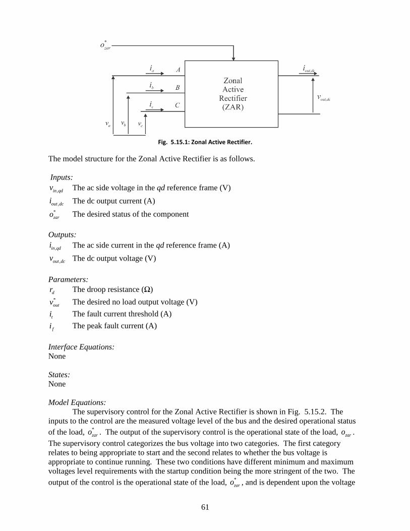
In this section, each of the component models needed to represent the MVAC, HFAC, and MVDC systems is represented.
5.1 Synchronous Reference Frame Estimator
The ac systems used herein feature multiple synchronous machines. Since the network equations must be solved in a single synchronous reference frame, the position of this reference frame must be defined. This model defines the position of the synchronous reference frame [5.1.1]. Note that this ‘model’ is different than most of the models in this report in that it does not represent a physical component. Rather, it defines the synchronous reference frame which is used for system analysis purposes. Nevertheless, it will be treated as if it were a component model for documentation purposes. Inputs:
rAGω Vector of angular electrical speeds of all active generators (rad/s) Outputs:
eω The estimated angular speed of the synchronous reference frame (rad/s) Parameters:
bAGP Vector of base power rating of all active generators (W) Interface Equations: None States: None Model Equations: The angular speed of the synchronous reference frame is a weighted average of the rotor speeds of all of the active generators. The weighting factor used is the base power of each generator. The calculation of the synchronous reference frame speed is found using
, ,
,
bAG i rAG ii AG
ebAG i
i AG
P
P
ωω ∈
∈
=∑
∑ (5.1.1)
Validation: This is not a component, but rather a definition. Hence validation is not relevant. References: [5.1.1] P. Krause, O. Wasynczuk, S. Sudhoff, and S. Pekarek, “Analysis of Electric Machinery
and Drive Systems,” 3rd Edition, New York: John Wiley and Sons/IEEE Press, 2013.
11
5.2 AC WRSM Generator Model
The ac wound rotor synchronous machine model in this work is that of a wound-field synchronous machine with two q-axis damper windings and one d-axis damper winding. The model is defined in [5.2.1] and outlined herein. The reduced order of the model refers to the neglecting of the fast stator dynamics in the model definition. The structure of the model is as follows.
Inputs:
eqdsv A vector of q- and d-axis terminal voltages ( e
qsv and edsv ) in the synchronous ref. frame (V)
rmω The mechanical rotor speed (rad/s)
fdv The referred field voltage (V)
eω The radian frequency of the synchronous reference frame (rad/s) Outputs:
eqdsi A vector of q- and d-axis currents ( e
qsi and edsi ) into the machine in the synchronous ref.
frame (A) eT The electrical torque of the machine (positive for motor operation) (Nm)
fdi The referred field current into the machine (A) Parameters:
sr The referred resistance of the stator windings (Ω)
1kqr The referred resistance of the 1st q-axis damper winding (Ω)
2kqr The referred resistance of the 2nd q-axis damper winding (Ω)
fdr The referred resistance of the d-axis field winding (Ω)
kdr The referred resistance of the d-axis damper winding (Ω)
mqL The q-axis mutual inductance (H)
mdL The d-axis mutual inductance (H)
1lkqL The referred leakage inductance of the 1st q-axis damper winding (H)
2lkqL The referred leakage inductance of the 2nd q-axis damper winding (H)
lfdL The referred leakage inductance of the d-axis field winding (H)
lkdL The referred leakage inductance of the d-axis damper winding (H) Interface Equations: The interface equation for the generator may be expressed
''
''
''
e e eqq qde e q
qds qdse e edq dd d
eeqdqd
Z Z eZ Z e
= +
v i
eZ
(5.2.1)
where
12
( )( )'' ''sin 22
e rqq s d qZ r L Lω δ= − − (5.2.2)
( ) ( )( )2'' '' '' sineqd r d d qZ L L Lω δ= − − (5.2.3)
( )( )'' ''sin 22
e rdq s d qZ r L Lω δ= + − (5.2.4)
( ) ( )( )2'' '' '' sinedd r q d qZ L L Lω δ= − − − (5.2.5)
and
( ) ( )( )'' '' ''sin cose
q r q de ω δ λ δ λ= + (5.2.6)
( ) ( )( )'' '' ''cos sined r q de ω δ λ δ λ= − + (5.2.7)
In (5.2.2) through (5.2.7), δ is the torque angle which is a state. The impedances in (5.2.2) through (5.2.5) have units of Ohms and the voltages in (5.2.6) through (5.2.7) have units of V. In (5.2.2) through (5.2.7),
1
''
1 2
1 1 1q ls
mq lkq lkq
L LL L L
−
= + + +
(5.2.8)
1
'' 1 1 1d ls
md lkd lfd
L LL L L
−
= + + +
(5.2.9)
and
1 2
1 2''
1 2
1
kq kqmq
lkq lkqq
mq mq
lkq lkq
LL LL LL L
λ λ
λ
+
=+ +
(5.2.10)
''
1
fdkdmd
lkd lfdd
md md
lkd lfd
LL LL LL L
λλ
λ
+
=+ +
(5.2.11)
Model States: δ Torque angle (rad)
13
1kqλ The referred Flux linkage of 1st q-axis damper winding (Vs)
2kqλ The referred Flux linkage of 2nd q-axis damper winding (Vs)
fdλ The referred Flux linkage of d-axis field winding (Vs)
kdλ The referred Flux linkage of d-axis damper winding (Vs)
Model Equations: The time derivative of the torque angle is calculated as
r eddtδ ω ω= − (5.2.12)
The time derivatives of the rotor states are found using the sequence
( )1 ''e e e eqds qd qds qd
−−=i Z v e (5.2.13)
( ) ( )( ) ( )
cos sinsin cos
e r δ δδ δ
− =
K (5.2.14)
r e r eqds qds=i K i (5.2.15)
( )
( )1 2 1 2 1
12 1 1
rlkq kq mq kq mq kq lkq mq qs
kqlkq lkq mq lkq mq
L L L L L ii
L L L L L
λ λ λ− + −=
+ + (5.2.16)
( )
( )2 1 2 1 2
21 2 2
rlkq kq mq kq mq kq lkq mq qs
kqlkq lkq mq lkq mq
L L L L L ii
L L L L L
λ λ λ− + −=
+ + (5.2.17)
( )
( )r
lfd kd md fd md kd lfd md dsfd
lkd lfd md lfd md
L L L L L ii
L L L L L
λ λ λ− + −=
+ + (5.2.18)
( )
( )r
lkd fd md kd md fd lkd md dskd
lfd lkd md lkd md
L L L L L ii
L L L L L
λ λ λ− + −=
+ + (5.2.19)
whereupon the time derivatives of the rotor states are found using
1
1 1kq
kq kq
dr i
dtλ
= − (5.2.20)
2
2 2kq
kq kq
dr i
dtλ
= − (5.2.21)
14
fdfd fd fd
dv r i
dtλ
= − (5.2.22)
kd
kd kdd r idtλ
= − (5.2.23)
The stator flux linkages are found
( )1 2r r
qs ls qs mq qs kq kqL i L i i iλ = + + + (5.2.24)
( )r rds ls ds md ds fd kdL i L i i iλ = + + + (5.2.25)
and the torque is calculated using
( )32 2
r re ds qs qs ds
PT i iλ λ= − (5.2.26)
Validation: This model has been widely used in the power engineering community for decades. Note that this model does not include saturation. Further, it is a reduced order model, so initial fault response will not be correctly predicted. References: [5.2.1] P. Krause, O. Wasynczuk, S. Sudhoff, and S. Pekarek, “Analysis of Electric Machinery
and Drive Systems,” 3rd Edition, New York: John Wiley and Sons/IEEE Press, 2013.
5.3 AC WRSM Exciter Model
The WRSM exciter model represents a rotating, rectifier type exciter based upon IEEEAC8B [5.3.1], and is depicted in Fig. 5.3.1.
Fig. 5.3.1: Synchronous Generator Exciter Model.
The model structure is as follows. Inputs:
qv The q-axis terminal voltage (V)
15
dv The d-axis terminal voltage (V) Outputs:
fdv The referred exciter voltage (V) Parameters:
refv The per-unit line-line reference voltage (pu)
PRK Automatic Voltage Regulator (AVR) proportional gain (pu)
IRK AVR integral gain (pu)
DRK AVR derivative gain (pu)
DRT AVR derivative time constant (s)
AK AVR power stage gain (pu)
AT AVR power stage time constant (s)
maxRv AVR positive ceiling voltage (pu)
minRv AVR negative ceiling voltage (pu)
ET Exciter field time constant (s)
EK Exciter field proportional gain (pu)
ratedv Rated line-line voltage of the synchronous machine (V) Interface Equations: None Model Equations: The model equations are not explicitly given here as they are readily formulated from Fig. 5.3.1. The per-unit line-line measured voltage is obtained from the q- and d-axis voltages using
2 232
q dc
rated
v vv
v+
= (5.3.1)
where ratedv is the rated rms line-neutral voltage of the synchronous machine.
The saturation block in Fig. 5.3.1 is defined as
( ) EBvES v Ae= (5.3.2)
where A (1.0119) and B (0.875) are calculated using selected points on the voltage saturation curve, i.e. the open-circuit voltage vs. exciter field voltage curve.
The physical field voltage is obtained by scaling VE, the per-unit value of the field voltage.
fd fd Ev k V= (5.3.3)
16
where 23 rated fd
fdr md
v rk
Lω=
(5.3.4)
Validation: This is a behavioral model commonly used in the power engineering community. However, it does not represent any physical excitation system. References: [5.3.1] L.M. Hajagos and M.J. Basler, "Changes to IEEE 421.5 recommended practice for
excitation system models for power stability studies", IEEE/PES 2005 Meeting, San Francisco, CA.
5.4 AC Generator Real Time Synchronization Controller
The AC generator synchronization controller is used for MVAC and HFAC systems, where synchronization of paralleled generators is important. In MVAC and HFAC power distribution systems for an Electric Ship, multiple AC generators are present. Depending on the system operating mode, the overall system may break up into unconnected subsystems – for example unconnected starboard and port busses fed by separate AC generators. At some point, system reconfiguration may cause previously disconnected parts of the electrical distribution system to be interconnected. This may lead to large transients if the overall system is not properly synchronized. This section describes a supervisory controller called Real-Time Synchronization Controller (RTSC), which solves this problem by keeping all parts of the electrical distribution system synchronized at all times, even when they are not electrically connected. This requires both frequency and phase synchronization for all AC generators. The RTSC accomplishes this by augmenting the conventional frequency droop control for generators. At any given time, one interconnected subsystem is considered the reference subsystem and all other systems are target subsystems. The RTSC forces the target subsystems to be phase-synchronized with the reference subsystem. For more information on the RTSC see [5.4.1]. The discussion refers to a set of generators, each consisting of a gas turbine, as described in Section 5.5, connected to an AC WRSM generator, as described in Sections 5.1 through 5.3. Inputs:
,rm refω Reference turbine speed (pu)
iP Output power of ith generator (W)
,refqdv A vector of q- and d-axis terminal voltages for the reference subsystem (V)
,targetqdv A vector of q- and d-axis terminal voltages for the target subsystem (V) Outputs:
ispeedω∆ Offset added to the common speed reference ,rm refω for the ith generator by the RTSC controller (pu)
Parameters:
17
iD Droop setting of speed regulator for ith generator (pu)
_rated iP Rated power of ith generator (W) 𝜔𝐼 Cutoff frequency of Low-Pass Filter I (rad/s) 𝜔𝐼𝐼 Cutoff frequency of Low-Pass Filter II (rad/s)
Model Equations:
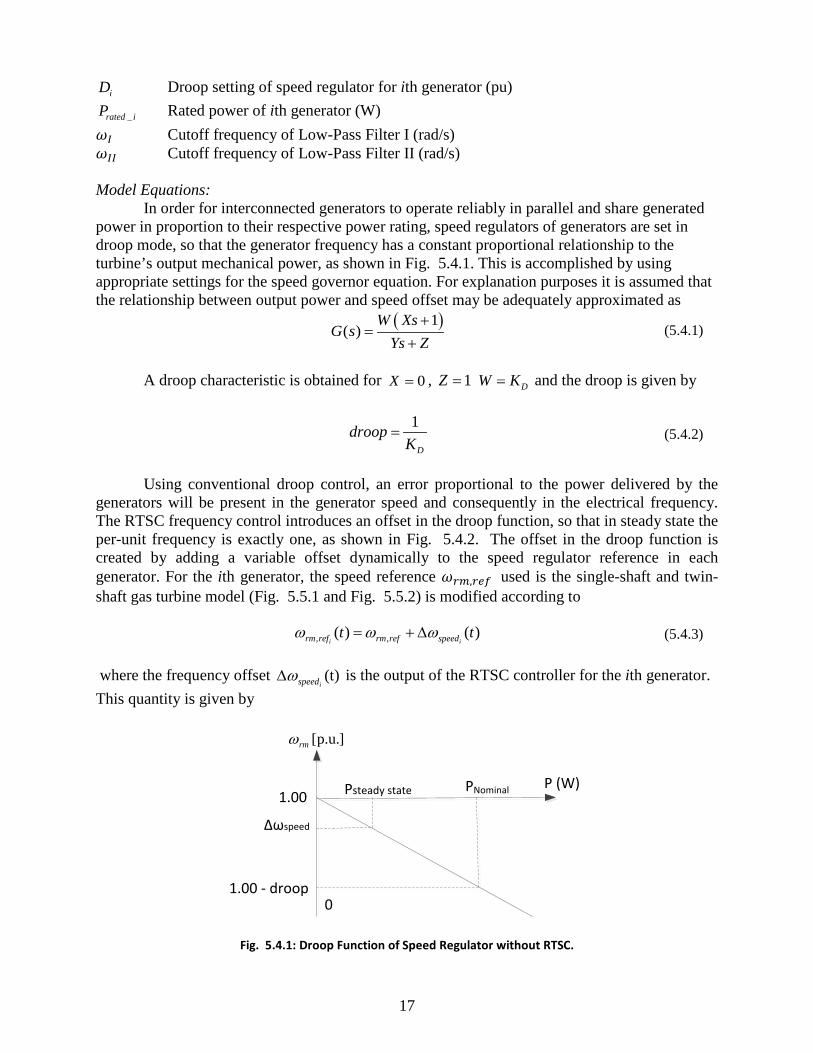
In order for interconnected generators to operate reliably in parallel and share generated power in proportion to their respective power rating, speed regulators of generators are set in droop mode, so that the generator frequency has a constant proportional relationship to the turbine’s output mechanical power, as shown in Fig. 5.4.1. This is accomplished by using appropriate settings for the speed governor equation. For explanation purposes it is assumed that the relationship between output power and speed offset may be adequately approximated as
( )1( )
W XsG s
Ys Z+
=+
(5.4.1)
A droop characteristic is obtained for 0X = , 1Z = DW K= and the droop is given by
1
D
droopK
= (5.4.2)
Using conventional droop control, an error proportional to the power delivered by the
generators will be present in the generator speed and consequently in the electrical frequency. The RTSC frequency control introduces an offset in the droop function, so that in steady state the per-unit frequency is exactly one, as shown in Fig. 5.4.2. The offset in the droop function is created by adding a variable offset dynamically to the speed regulator reference in each generator. For the ith generator, the speed reference 𝜔𝑟𝑚,𝑟𝑒𝑓 used is the single-shaft and twin-shaft gas turbine model (Fig. 5.5.1 and Fig. 5.5.2) is modified according to
ispeedω∆ is the output of the RTSC controller for the ith generator. This quantity is given by
1.00
1.00 - droop0
PNominal P (W)
∆ωspeed
Psteady state
]p.u.[rmω
Fig. 5.4.1: Droop Function of Speed Regulator without RTSC.
18
1.00
0
PNominal P (W)Psteady state1.00 + ∆ωspeed
1.00 – droop + ∆ωspeed
]p.u.[rmω
Fig. 5.4.2: Droop Function of Speed Regulator With RTSC.
1
_1
( )( )
i
n
ij jj
speed i n
ij rated jj
K P tt D
K Pω =
=
∆ = ⋅∑
∑ (5.4.4)
where iD is the droop setting of the speed regulator in the ith Generator, 𝑃𝑟𝑎𝑡𝑒𝑑_𝑗 is the rated active power of the jth Generator, 𝑃𝑗(𝑡) is the instantaneous output power of the jth Turbine Engine, 𝐾𝑖𝑗 represents the relationship between the Generators i and j: 𝐾𝑖𝑗 = 1 if the two generators are located in the same subsystem; 𝐾𝑖𝑗 = 0 if the two generators are located in different subsystems; 𝑛 is the total number of generators in the ESPS. The RTSC controller can determine the values of ijK based on the status of the circuit breakers on the power distribution busses. The ratio on the right hand side of (5.4.4) represents the percentage loading of the generators in the subsystem containing Generator 𝑖 with respect to their combined rated power. When implementing the RTSC in an ESPS, one subsystem is chosen as the reference subsystem and the other subsystems are set as the target subsystems. The criterion to choose reference subsystem is that it should have the largest power rating among all subsystems. As the control is implemented in software, the reference subsystem can be chosen dynamically according to system operating state. The complete structure of the RTSC is shown in Fig. 5.4.3.
19
Fig. 5.4.3: Structure of the RTSC Consisting of Frequency Control and Phase Control.
In the figure only two subsystems are shown for simplicity: a reference subsystem, consisting of Generators 1 – m, and a target subsystem, consisting of Generators m+1 – n. Additional subsystems would be shown as separate target subsystems. Both the reference and the target subsystem have Frequency Control, but only the target subsystem has Phase Control. The goal of Phase Control is to keep voltages of the target subsystem and the reference subsystem in phase at all times.
Inside the Frequency Control part of the controller, the frequency offset block calculates for each generator the frequency offset as a function of real power generated using (5.4.4). The frequency offset goes through a first-order lowpass filter called Low-Pass Filter II, having the form
1( )1
LPF II
II
G s sω
− =+
(5.4.5)
20
For generators 1 – m belonging to the reference subsystem, this offset is added to the speed reference as in (5.4.3). For generators m+1 – n belonging to the target subsystem, the RTSC control includes also phase control. In the Phase Control part of the controller, quantities ,refqdv and ,targetqdv are the vectors of q- and d-axis voltages for the reference and the target subsystem, respectively. Low-Pass Filter I (LPF-I) is a first-order lowpass filter used to eliminate the harmonics resulting from non-linear load current and it has the form
1( )
1LPF I
I
G s sω
− =+
(5.4.6)
For a generator having q-axis terminal voltage qv and d-axis terminal voltage dv , the Phase Calculation block calculates the absolute phase as
( )atan 2 ,v d qv vθ = (5.4.7)
The phase difference between the target subsystem and the reference subsystem voltages is calculated as
,target ,refv v vθ θ θ∆ = − (5.4.8) and sent to the Signal Processing block, which constrains its value from [-2π, 2π] to [-π, π] using phase wrap. The phase control offset is produced by the Gain block in Fig. 5.4.3 and is added to the frequency control offset. For details on the design of Low-Pass Filter I and Low-Pass Filter II, please refer to [5.4.1].
As a result of the RTSC control of Fig. 5.4.3 in steady state all subsystems operate at the nominal frequency (p.u. frequency of one) and the voltages of all target subsystems are in phase with the reference subsystem.
Validation:
This component model is of a control, not of a physical component. Therefore, it has to be considered in terms of effectiveness, not fidelity. The reader is referred to [5.4.1] for a discussion of the effectiveness of this control. References: [5.4.1] E. Santi, and Y. Zhang, “Design of Real-Time Synchronization Controller in Electric
Ship Power Systems,” ESRDC Report, 2013. [5.4.2] W.I. Rowen, “Simplified Mathematical Representations of Heavy-duty Gas Turbines”,
Journal of Engineering for Power, Vol. 105, 1983.
5.5 Generic Prime Mover Model
The gas turbine models used in this work consist of speed and acceleration control loops. The temperature control often associated with this type of gas turbine representation is omitted herein based upon the assumption that the critical turbine temperature will not be reached since
21
temperature changes occur mostly during the startup of the turbine. The transfer function representing the speed governor allows for either droop or isochronous control. Setting the speed governor transfer function coefficient X=0 results in droop control where the output of the governor is directly proportional to the speed error, as can be seen in the turbine model diagrams in Fig. 5.5.1 and Fig. 5.5.2.
5.5.1 Single-shaft Gas Turbine
The single-shaft gas turbine model is depicted in Fig. 5.5.1.
The structure of the turbine model is as follows. Inputs:
flbK Fuel control parameter (pu) a,b,c Valve control parameters (pu)
fsτ Fuel system time constant (s)
cT Combustor time delay (s)
cpτ Compressor time constant (s) Interface Equations: None
22
Fig. 5.5.1: Generic Single-Shaft Gas Turbine Model [5.5.1].
23
Model Equations: The per unit turbine speed is found by dividing by the nominal speed of the turbine. The output torque, mT in per-unit, is calculated using the turbine torque function [5.5.1]
( ) ( ),1 1 1
2m pu f fla rmflb
T KK
ω ω= − + − (5.5.1)
where fω is the output of the compressor block and the turbine shaft speed, rmω , is in per-unit. The actual torque in Nm is obtained using
,Nm ,m t m puT k T= (5.5.2) where
tPkω
= nominal
nominal
(5.5.3)
This gas turbine model and the overall parameters of the model can be different for gas turbines built by different manufacturers; however, the general model structure is an adequate representation for describing the dynamic behavior of a single-shaft gas turbine. Validation:
The validity of this model is discussed in [5.5.1]. References: [5.5.1] W.I. Rowen, “Simplified mathematical representations of heavy-duty gas turbines”,
Journal of Engineering for Power, Vol. 105, 1983.
5.5.2 Twin-shaft Gas Turbine
The model for the twin-shaft gas turbine is similar to the single-shaft gas turbine but with an additional control loop for the engine speed [5.5.2] and is depicted in Fig. 5.5.2.
flaK , flbK Fuel control parameters (pu) a,b,c Valve control parameters (pu)
fsτ Fuel system time constant (s)
cT Combustor time delay (s)
cpτ Compressor time constant (s)
gH Engine shaft inertial constant (pu)
Interface Equations: None Model Equations: The per-unit turbine speeds are converted to per-unit by dividing by the nominal turbine speed. The per-unit torque is converted to Nm using (5.5.2) and (5.5.3). The free turbine torque is calculated
( ) ( )1 0.6 1m f fla rmflb
T KK
ω ω= − + − (5.5.4)
The engine torque is calculated
( ) ( )1 3 1mg f fla gflb
T KK
ω ω= − + − (5.5.5)
The engine speed request is calculated
, 1 2g ref fp pω ω= + (5.5.6)
Validation: The validity of this model is discussed in [5.5.2].
References: [5.5.2] L.N. Hannet, G. Jee, and B. Fardanesh, “A governor/turbine model for a twin-shaft
combustion turbine,” IEEE Transactions on Power Systems, Vol. 10, no.1, pp. 133-140.
26
5.6 DC WRSM Generator Model
The dc WRSM model is depicted in Fig. 5.6.1 and consists of a WRSM connected to load commutated rectifier through an ac circuit breaker (CB). The component model is set forth in [5.6.1] and outlined herein.
rmω The mechanical rotor speed of the machine (rad/s)
fdv The referred field voltage (V) *gcbo The desired status of the generator circuit breaker
Outputs:
dcv The dc output voltage of the generator (V)
eT The electrical torque of the machine (positive for motor operation) (Nm)
fdi The referred field current into the machine (A) Parameters:
,mindcv The dc bus voltage threshold (V) glfi The load current fault threshold (A)
lL DC link inductance (H) C DC link capacitance (F)
sr The resistance of the stator windings (Ω)
1kqr The referred resistance of the 1st q-axis damper winding (Ω)
2kqr The referred resistance of the 2nd q-axis damper winding (Ω)
fdr The referred resistance of the d-axis field winding (Ω)
kdr The referred resistance of the d-axis damper winding (Ω)
mqL The q-axis mutual inductance (H)
27
mdL The d-axis mutual inductance (H)
1lkqL The referred leakage inductance of the 1st q-axis damper winding (H)
2lkqL The referred leakage inductance of the 2nd q-axis damper winding (H)
lfdL The referred leakage inductance of the d-axis field winding (H)
lkdL The referred leakage inductance of the d-axis damper winding (H) Interface Equations: None Model States:
dcv The dc output voltage of the generator (V)
dci The dc current through the dc link inductor (V)
1kqλ The referred Flux linkage of 1st q-axis damper winding (Vs)
2kqλ The referred Flux linkage of 2nd q-axis damper winding (Vs)
fdλ The referred Flux linkage of d-axis field winding (Vs)
kdλ The referred Flux linkage of d-axis damper winding (Vs) Model Equations:
The model equations for this component are broken in to six subsections. First, the subtransient model is defined, followed by the calculation of the firing and commutation angles. The third section considers the calculation of the stator currents and the fourth and fifth sections define the machine and dc link dynamics respectively. The final subsection relates to the exciter model.
5.6.1 Subtransient Model
It is useful to represent the reduced-order synchronous machine stator voltage equations in voltage-behind-reactance form utilizing subtransient quantities when coupled with a rectifier. For a synchronous machine with two q-axis damper windings and one d-axis damper winding, the subtransient inductances and flux linkages are expressed [5.6.1]
1
''
1 2
1 1 1q ls
mq lkq lkq
L LL L L
−
= + + +
(5.6.1)
1
'' 1 1 1d ls
md lkd lfd
L LL L L
−
= + + +
(5.6.2)
1 2
1 2''
1 2
1
kq kqmq
lkq lkqq
mq mq
lkq lkq
LL LL LL L
λ λ
λ
+
=+ +
(5.6.3)
28
''
1
fdkdmd
lkd lfdd
md md
lkd lfd
LL LL LL L
λλ
λ
+
=+ +
(5.6.4)
5.6.2 Firing Angle and Commutation Angle Calculations
The second step in modeling this system is the calculation of the firing angle and commutation angle. Assuming that that the circuit breaker is closed, the calculation of the firing angle ( β ) relative to rotor position is discussed in [5.6.1] and outlined herein. For uncontrolled operation the firing angle relative to rotor position is equal to minβ which is found by solving
( ) ( )'' '' '' ''min min min
ˆ3 cos sin 2 sin 2 03q d dc q di L L πλ β λ β β + + − − =
(5.6.5)
An intermediate variable K is the found by solving
( ) ( ) ( )'' '' '' '' '' ''2 1 ˆ3 sin cos cos 23 2q d d q q d dcK L L L L iπλ β λ β β = − + + − + − +
(5.6.6)
Whereupon the commutation angle, µ , is found by solving
( ) ( )
( ) ( )
'' ''
'' '' '' ''
3 sin cos
2 1 ˆcos 2 2 03 2
q d
q d q d dc
K
L L L L i
λ β µ λ β µ
πβ µ
− − + + + − − + − + + =
(5.6.7)
In the event that the circuit breaker is open, then minβ , K, and µ can all be set to zero as
they are unused.
5.6.3 Calculation of Stator Currents
The next step in the modeling of the system is the calculation of the average q and d axis currents. In the case that the circuit breaker is open, the q- and d-axis currents are set to zero. If the circuit breaker is closed, they are calculated using the following procedure.
The average values of the q and d axis currents are broken into commutation and conduction components. First, the conduction components are obtained using
,2 3 2ˆ ˆ cos cos
3 3qs cond dci i π πβ β µπ
= + − + + (5.6.8)
,2 3 2ˆ ˆ sin sin
3 3ds cond dci i π πβ β µπ
= + − + + (5.6.9)
29
During the interval following the firing of valve 3, the a-phase current is given by
( ) ( ) ( )( )( ) ( ) ( )
( ) ( )( ) ( ) ( )
'' ''
as '' '' '' ''
'' '' '' ''
'' '' '' ''
3 sin cosi
cos 2 2
2 1 ˆcos 2 23 2cos 2 2
q r d r
rq d q d r
q d r q d dc
q d q d r
K
L L L L
L L L L i
L L L L
λ θ β λ θ βθ
θ β
πθ β
θ β
+ + − +=
+ − − +
− + − + + −+ − − +
(5.6.10)
where rθ is the electrical rotor position offset such that valve 3 fires when rθ = 0. The q and d axis currents can be expressed in terms of the a-phase current as
( ) ( ) ( )qs as2 3 ˆi i sin sin
3 3r r r dc ri πθ θ θ β θ β = − + − + + (5.6.11)
( ) ( ) ( )ds as2 3 ˆi i cos cos
3 3r r r dc ri πθ θ θ β θ β = + + + + (5.6.12)
Therefore, the commutation component of the average q and d axis currents is given by
( ) ( ), qs qs qs qs qs3ˆ i 0 4i 2i 4i i
4 4 2 4qs comi µ µ µ µ µπ
= + + + + (5.6.13)
( ) ( ), ds ds ds ds ds3ˆ i 0 4i 2i 4i i
4 4 2 4ds comi µ µ µ µ µπ
= + + + + (5.6.14)
and the average q and d axis currents are found using
, ,ˆ ˆ ˆqs qs cond qs comi i i= + (5.6.15)
, ,ˆ ˆ ˆds ds cond ds comi i i= + (5.6.16)
5.6.4 Machine Dynamics
The next step is to calculate the flux linkages, the derivative of flux linkages, and the electrical torque of the machine which can be written as
'' ''ˆ
qs q qs qL iλ λ= + (5.6.17)
'' ''ˆds d ds dL iλ λ= + (5.6.18)
30
( )1 1 '' ''1
1
ˆ ˆkq kqkq q qs q ls qs
lkq
d rL i L i
dt Lλ
λ λ−
= − − + (5.6.19)
( )2 2 '' ''2
2
ˆ ˆkq kqkq q qs q ls qs
lkq
d rL i L i
dt Lλ
λ λ−
= − − + (5.6.20)
( )'' ''ˆ ˆkd kdkd d ds d ls ds
lkd
d r L i L idt Lλ λ λ−
= − − + (5.6.21)
( )'' ''ˆ ˆfd fdfd fd d ds d ls ds
lfd
d rv L i L i
dt Lλ
λ λ= − − − + (5.6.22)
The electrical torque of the synchronous machine (positive for generator operation) is found using
( )3 ˆ ˆ2 2e ds qs qs ds
PT i iλ λ= − − (5.6.23)
The mechanical dynamics of the synchronous machine generator are expressed
rmg pm e
dJ T Tdtω
= − (5.6.24)
where Tpm is the prime mover torque.
5.6.5 DC Link Dynamics
The dc link dynamics are computed by first computing the commutating inductance Lc is given by
( ) ( ) ( )'' '' '' ''1 sin 22 6c q d d qL L L L L πβ β = + + − +
(5.6.25)
and the transient commutating inductance expressed
( ) ( )'' '' '' '' sin 26t q d d qL L L L L πβ β = + + − −
(5.6.26)
The magnitude of the subtransient voltage is given by
( ) ( )2 2'' ''r q dE ω λ λ= + (5.6.27)
which is obtained from
'' ''q r de ω λ= (5.6.28)
31
'' ''d r qe ω λ= − (5.6.29)
Next, the phase angle of the subtransient voltage is calculated as
( )'' ''angle d qjφ λ λ= − (5.6.30) which is obtained from (5.6.28), (5.6.29), and
( )'' "angle q de jeφ = + (5.6.31) whereupon the firing angle relative to the voltage is given by
α β φ= − (5.6.32)
The time derivative of the average dc current is expressed as
( )
( )
3 3 3 ˆˆcos3 3ˆ ˆ( 0) cos
ˆ 3 3ˆ ˆ ˆ( 0) cos
ˆˆ ˆ( 0)
ˆ ˆ( 0)
dc l r c dc
g dc dcl t
dcdc g dc dc
dc l dcg dc
l
dc g dc
E v r L ic i E v
L L
diki c i E v
dt
v r i c iLki c i
α ω βπ π α
β π
απ
− − + ⋅ > + > + = − ⋅ > + >
− − ⋅ >
− ⋅ ≤
(5.6.33)
In (5.6.33), k is an artificial constant used to drive the dc link current to zero. The time derivative of the capacitor voltage is found as
( )
( )
ˆˆˆ 0 ( )ˆ
ˆˆ ˆ 0 ( )
dc gldc dc gldc
dc dc dc gl
i iv i idv C
dtkv v i i
−> + >
= − > + >
(5.6.34)
The terms to the right in (5.6.33) and (5.6.34) are Boolean, and that the over-bar denotes logical complement.
5.6.6 Generator Circuit Breaker Control
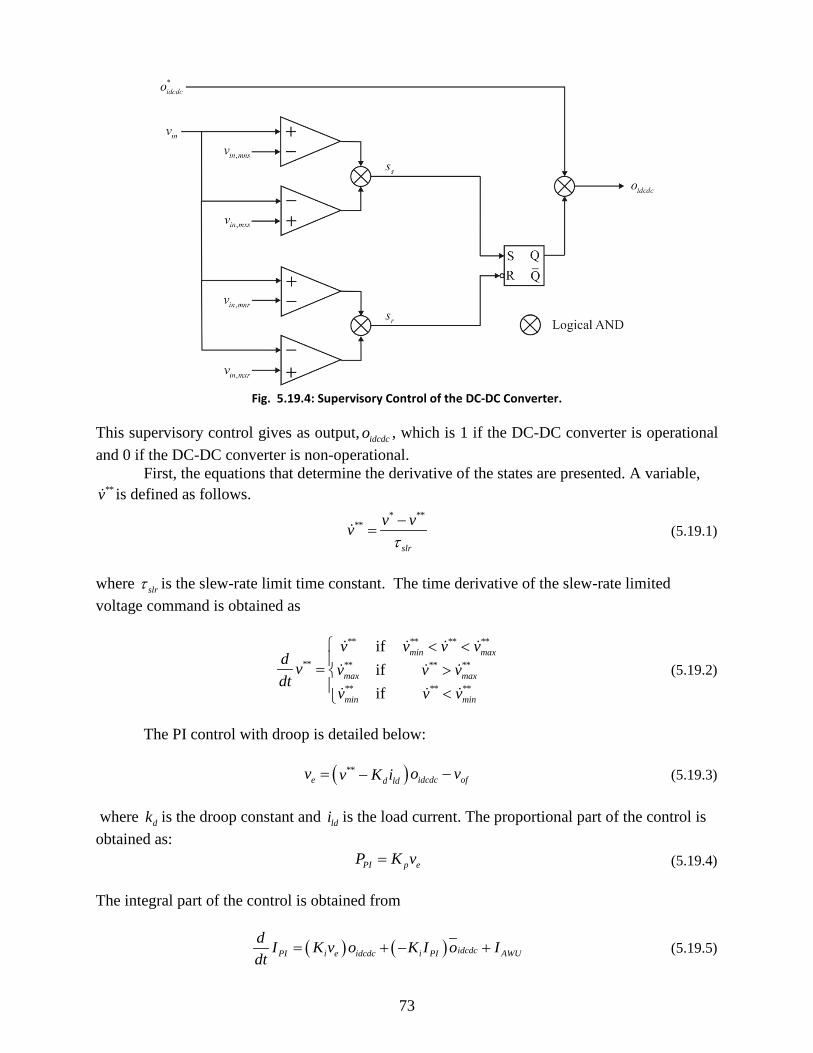
The circuit breaker control is depicted in Fig. 5.6.2. The inputs to the control are the desired status of the breaker, *
gcbo , the dc voltage, dcv , the minimum dc voltage, ,mindcv , the load
32
current, gli , and the fault current threshold, glfi . The output of the control is the circuit breaker status, gc .
Fig. 5.6.2: DC Generator Circuit Breaker Control.
When a fault occurs the load current will rise above the fault current threshold causing the breaker status to go low and the breaker to open. In order to check if the fault is cleared, a low voltage supply is placed on the dc bus to trickle charge it. If there is no fault, then the dc voltage will rise above the minimum dc voltage value and, assuming the desired circuit breaker state is high, the circuit breaker will close. If the fault is still in place, the dc voltage will not rise and the circuit breaker will remain open.
Validation:
The generator rectifier model has been used extensively. It may be rigorously derived, and has been shown to accurately predict experimentally observed results. The main limitation is for very heavily loaded cases in which the thyristor conduction pattern changes. References: [5.6.1] Sudhoff, S.D.; Corzine, K. A.; Hegner, H.J.; Delisle, D.E., "Transient and dynamic
average-value modeling of synchronous machine fed load-commutated converters," Energy Conversion, IEEE Transactions on , vol.11, no.3, pp.508,514, Sep 1996.
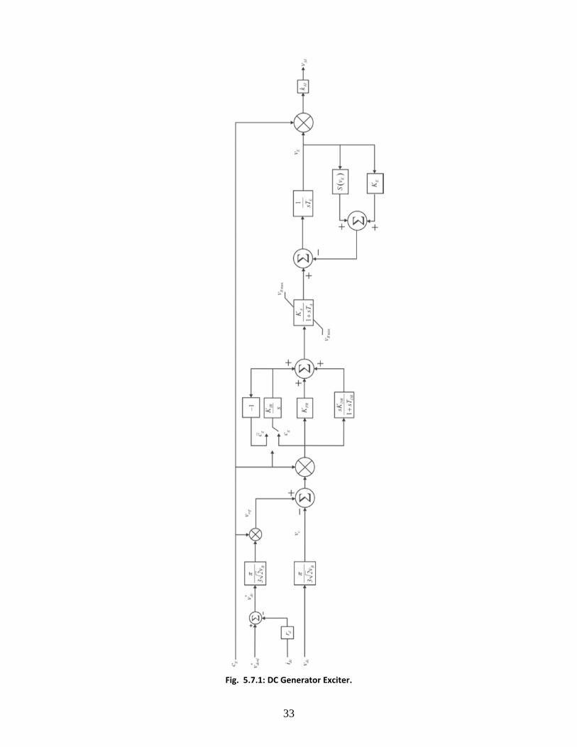
5.7 DC WRSM Exciter Model
The dc generator exciter is based upon IEEE AC8B [5.7.1] and is depicted in Fig. 5.7.1.
33
Fig. 5.7.1: DC Generator Exciter.
34
Inputs:
gc Circuit breaker status (1 is closed, 0 is open)
dci The measured dc current (A)
dcv The measured dc voltage (V) Outputs:
fdv The referred exciter voltage (V) Parameters:
*dcnlv The no load dc voltage (V)
ratedv The rated dc link voltage (V)
Bv Base voltage (V)
dr Droop resistance (Ω)
PRK Automatic Voltage Regulator (AVR) proportional gain (pu)
IRK AVR integral gain (pu)
DRK AVR derivative gain (pu)
DRT AVR derivative time constant (s)
AK AVR power stage gain (pu)
AT AVR power stage time constant (s)
maxRv AVR positive ceiling voltage (pu)
minRv AVR negative ceiling voltage (pu)
ET Exciter field time constant (s)
EK Exciter field proportional gain (pu) Interface Equations: None Model Equations: The droop resistance is found
* *dcnl dcfl
ddcfl
v vr
i−
= (5.7.1)
in which *
dcflv is the desired full load voltage and dcfli is the full load dc current. The reference voltage for the exciter, refv , is determined by converting the desired dc
voltage, *dcv , to the rms line-line representation needed by the exciter. The desired dc voltage is
obtained as the difference of the desired no load dc voltage and the dc current multiplied by dr . The reference voltage is modulated by the circuit breaker status, gc . The measured bus voltage for the exciter, Cv , is obtained as the rms line-line representation of the measured dc voltage.
35
The model equations for the exciter are not explicitly given here as they are readily formulated from Fig. 5.7.1.
The saturation block is defined as
0.875( ) 1.0119 EvES v e= (5.7.2)
The integral term of the PI control is switched between either the error between the
measured and reference voltages, or the negative of the integral term based upon the status of the circuit breaker. This winds down the integral term of the control if the circuit breaker opens due to a fault.
The referred field voltage is obtained from the per-unit field voltage Ev using
fd g fd Ev c k v= (5.7.3)
where fdk is defined by (5.3.4). Validation:
This is a behavioral model commonly used in the power engineering community to represent a rotating-rectifier type exciter and is discussed in [5.7.1]. References: [5.7.1] L.M. Hajagos and M.J. Basler, "Changes to IEEE 421.5 recommended practice for
excitation system models for power stability studies", IEEE/PES 2005 Meeting, San Francisco, CA.
5.8 Propulsion Drive Model
The propulsion drive consists of a dc link, an inverter, and a permanent magnet synchronous machine as depicted in Fig. 5.8.1. In ac applications, this drive modeled is used in conjunction with the rectifier model presented in the following section.
The dc link consists of a capacitor dcC and a braking resistor rbr . The inverter is an active current controlled inverter driving a slightly salient permanent magnet synchronous machine.
Fig. 5.8.1: DC Propulsion Drive.
36
The model structure is as follows Inputs:
dcv The dc bus voltage (V)
rmω The mechanical speed of the propulsion drive (rad/s) *pdo The desired operational status of the drive *rmω The desired mechanical speed of the propulsion drive (rad/s)
,estLT The estimated load torque of the propulsion drive (Nm) Outputs:
qsv The q-axis voltage of the propulsion motor (V)
dsv The d-axis voltage of the propulsion motor (V)
iP The power drawn from the inverter (W)
qsi The q-axis current into the propulsion motor (A)
dsi The d-axis current into the propulsion motor (A)
eT The output electrical torque of the propulsion motor (Nm) Parameters: P The number of poles in the PMAC
mλ The flux linkage due to the permanent magnet (Vs)
qL The q-axis inductance of the machine (H)
dL The d-axis inductance of the machine (H)
sr The stator resistance of the machine (Ω)
dcC The dc link capacitance value (F)
rbr The resistor brake resistance value (Ω)
pK The speed control proportional gain Nmrad/s
iK The speed control integral gain Nmrad
rmrω The rated mechanical speed of the drive (rad/s)
mxT The maximum allowable commanded torque (Nm)
mnT The minimum allowable commanded torque (Nm)
emxiT The maximum rate of change in commanded torque (Nm/s)
emniT The minimum rate of change in commanded torque (Nm/s)
nscτ The non-linear stabilizing control time constant (s)
fmxv The maximum non-linear stabilizing control voltage (V)
fmnv The minimum non-linear stabilizing control voltage (V)
nscn The order of the non-linear stabilizing control
iv∆ An allowed margin for error in the inverter voltage (V)
37
Interface Equations: States:
cv The dc link capacitor voltage (V) Model Equations:
5.8.1 PMAC Motor and Drive Model
The propulsion motor is a slightly salient PMSM. The model for this machine is defined in [5.8.1] and outlined herein. First, the electrical speed of the machine is
2r rmPω ω= (5.8.1)
where rmω is the mechanical speed of the machine, and P is the number of poles. The machine model is defined using a qd0 framework in the rotor reference frame. The reduced-order voltage equations in the rotor reference frame are presented in qd form as
r r rqs s qs r d ds r mv r i L iω ω λ= + + (5.8.2)
r r rds s ds r q qsv r i L iω= − (5.8.3)
where is the stator winding resistance, qL and dL are the q and d axis inductances, mλ is the flux linkage due to the permanent magnet, and rω is the angular velocity of the rotor. The inverter considered is an active current controlled inverter and so the currents obtained can be assumed to be the desired currents. Therefore the q and d axis currents are obtained using
*4
30
epdr
mqs
pd
T oPi
oλ
=
(5.8.4)
( )
( )2
0 or
4 and
2
pd aiv riv
rds fw fw fw fw
pd aiv rivfw
o v v
i b b a co v v
a
≥= − + −
<
(5.8.5)
where pdo is the operational status of the drive, aivv is the available inverter voltage, rivv is the required inverter voltage, and fwa , fwb , and fwc are defined as
2 2 2fw s r da r Lω= + (5.8.6)
2( ) 2r r
fw s qs r m r d s qs q rb r i L r i Lω λ ω ω= + − (5.8.7)
sr
38
2 21 ( )
3fw ri aivc v v= − (5.8.8)
The available inverter voltage is
aiv i iv v v= − ∆ (5.8.9)
where iv∆ represents an allowed margin. The required inverter voltage is
2 23 ( ) ( )r r
riv s qs r m r q qsv r i L iω λ ω= + + (5.8.10)
The inverter power is then found using
( )32
r r r ri qs qs ds dsP v i v i= + (5.8.11)
and the inverter current is
0
ipd
ii
pd
P ovi
o
=
(5.8.12)
5.8.2 DC Link and Resistor Brake
The dc link in the propulsion drive is depicted in Fig. 5.8.2. The dc link consists of a capacitor and the braking resistor.
Fig. 5.8.2: DC Link.
The equations defining the dc link are
c C
dc
dv idt C
= (5.8.13)
39
0 0
1
rb
rb outrb
rb
i vr
ο
ο
== =
(5.8.14)
in C rb outi i i i= + + (5.8.15)
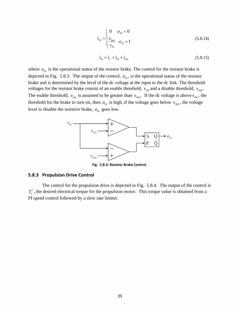
where rbo is the operational status of the resistor brake. The control for the resistor brake is depicted in Fig. 5.8.3. The output of the control, rbo , is the operational status of the resistor brake and is determined by the level of the dc voltage at the input to the dc link. The threshold voltages for the resistor brake consist of an enable threshold, rbev and a disable threshold, rbdv . The enable threshold, rbev is assumed to be greater than rbdv . If the dc voltage is above rbev , the threshold for the brake to turn on, then rbo is high, if the voltage goes below rbdv , the voltage level to disable the resistive brake, rbo goes low.
Fig. 5.8.3: Resistor Brake Control.
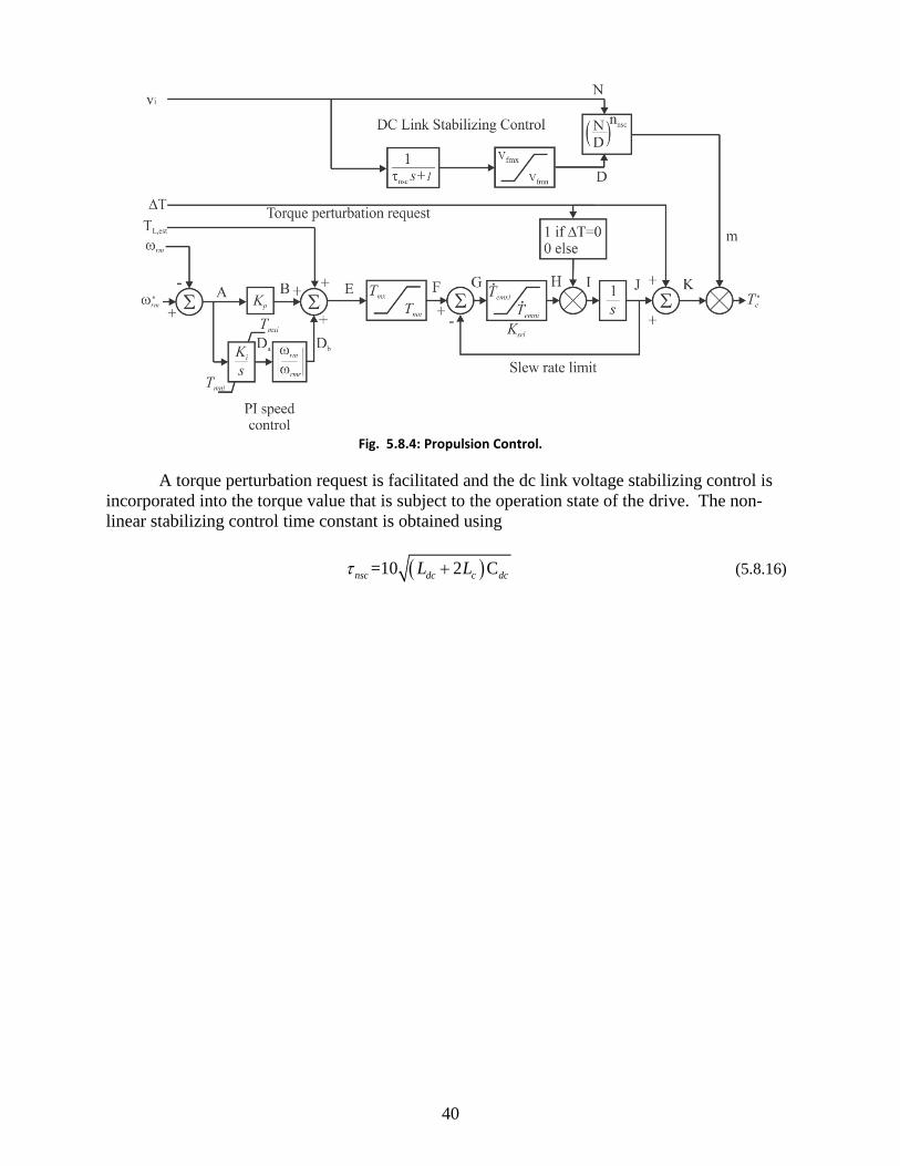
5.8.3 Propulsion Drive Control
The control for the propulsion drive is depicted in Fig. 5.8.4. The output of the control is *
eT , the desired electrical torque for the propulsion motor. This torque value is obtained from a PI speed control followed by a slew rate limiter.
40
Fig. 5.8.4: Propulsion Control.
A torque perturbation request is facilitated and the dc link voltage stabilizing control is incorporated into the torque value that is subject to the operation state of the drive. The non-linear stabilizing control time constant is obtained using
( )=10 2 Cnsc dc c dcL Lτ + (5.8.16)
41
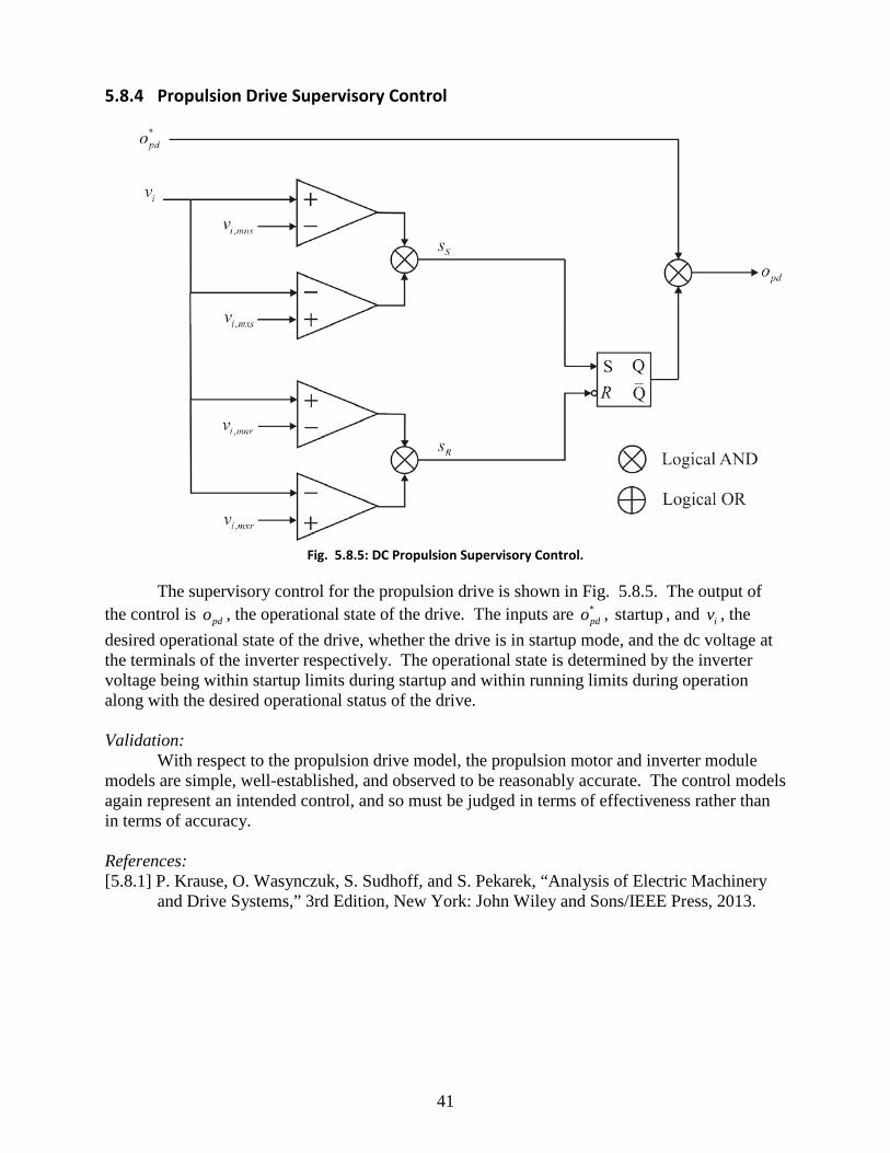
5.8.4 Propulsion Drive Supervisory Control
Fig. 5.8.5: DC Propulsion Supervisory Control.
The supervisory control for the propulsion drive is shown in Fig. 5.8.5. The output of the control is pdo , the operational state of the drive. The inputs are *
pdo , startup , and iv , the desired operational state of the drive, whether the drive is in startup mode, and the dc voltage at the terminals of the inverter respectively. The operational state is determined by the inverter voltage being within startup limits during startup and within running limits during operation along with the desired operational status of the drive. Validation: With respect to the propulsion drive model, the propulsion motor and inverter module models are simple, well-established, and observed to be reasonably accurate. The control models again represent an intended control, and so must be judged in terms of effectiveness rather than in terms of accuracy. References: [5.8.1] P. Krause, O. Wasynczuk, S. Sudhoff, and S. Pekarek, “Analysis of Electric Machinery
and Drive Systems,” 3rd Edition, New York: John Wiley and Sons/IEEE Press, 2013.
42
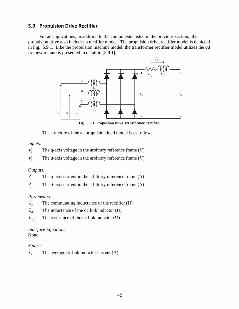
5.9 Propulsion Drive Rectifier
For ac applications, in addition to the components listed in the previous section, the propulsion drive also includes a rectifier model. The propulsion drive rectifier model is depicted in Fig. 5.9.1. Like the propulsion machine model, the transformer rectifier model utilizes the qd framework and is presented in detail in [5.9.1].
The structure of the ac propulsion load model is as follows. Inputs:
aqv The q-axis voltage in the arbitrary reference frame (V) adv The d-axis voltage in the arbitrary reference frame (V)
Outputs:
aqi The q-axis current in the arbitrary reference frame (A) aqi The d-axis current in the arbitrary reference frame (A)
Parameters:
cL The commutating inductance of the rectifier (H)
dcL The inductance of the dc link inductor (H)
Ldcr The resistance of the dc link inductor (Ω) Interface Equations: None States:
dci The average dc link inductor current (A)
43
Model Equations: The model inputs are the q and d axis voltages of the ac input in the arbitrary reference
frame and the outputs are the q and d axis currents in that same reference frame. To facilitate this, the frame-to-frame transformation
g a g a
qd qd =f K f (5.9.1)
is used where
( ) ( )( ) ( )
cos sin
sin cos
ga gaa g
ga ga
θ θ
θ θ
− =
K (5.9.2)
and where ‘g’ denotes a generator reference frame wherein the q-axis voltage is positive and the d-axis voltage is zero. Applying (5.9.2) with
( )angle a aga q dv jvθ = − − (5.9.3)
yields 2g
qv E= (5.9.4) and
0gdv = (5.9.5)
where 2 21
2a aq dE v v= + (5.9.6)
In (5.9.3) and (5.9.6), a
qv and adv are the q and d axis voltages to the left of the ac side inductor
cL in Fig. 5.9.1. The average dc voltage to the right of the rectifier is defined as
( )ˆ3 6 3 ˆˆ cos 2 dc
r C g dc cdiv E L i Ldt
α ωπ π
= − − (5.9.7)
where α is the firing delay angle. This average dc voltage can be related to dce by
ˆˆˆ dc
r Ldc dc dc dcdiv r i L edt
= + + (5.9.8)
Therefore
( )3 6 3 ˆcosˆ
2
Ldc c g dc dc
dcdc c
E r L i epi
L L
α ωπ π
− + − =
+
(5.9.9)
The derivative of the average dc current is expressed
(5.9.10)
44
ˆˆ fˆ fdcdc
dc
pididt ki
= −
where f is
( ) ( )ˆ ˆ0 0dc dcf i pi= ≥ ∪ > (5.9.11)
and k is a constant.
The commutation angle is determined using the following. First, assuming a firing delay angle of zero,
0sα = (5.9.12) The commutation angle is found using
( )ˆ2
acos cos6
c g dcs s s
L iE
ωµ α α
= − + −
(5.9.13)
This expression is only valid if several conditions are met. First,
( )ˆ2cos 1
6c e dc
sL i
Eωα − ≤ (5.9.14)
The second and third conditions are that 3sπµ ≤ and that s sµ α π+ ≤ . If these conditions are
met, then the firing delay angle and commutation angle are
sα α= (5.9.15)
and
sµ µ= (5.9.16) Otherwise the firing delay angle and commutation angle are taken to be
ˆ2
acos bound 1,1,3 6
c g dcL iE
ωπα = − −
(5.9.17)
and
3πµ = (5.9.18)
The expressions (5.9.17) and (5.9.18) assume 3-3 mode rectifier operation.
The first step in the calculation of the q and d axis currents is the calculation of the commutation interval currents defined as
(5.9.19)
45
,2 3 5 5ˆ ˆ sin sin
6 6
3 2 cos( )[cos( ) cos( )]
1 3 2 [cos(2 ) cos(2 2 )]4
gqg com dc
c g
c g
i i
EL
EL
π πµ α απ
α µ α απ ω
α α µπ ω
= + − − −
+ + −
+ − +
,2 3 5 5ˆ ˆ cos cos
6 6
3 2 cos( )[sin( ) sin( )]
1 3 2 3 2 1[sin(2 ) sin(2 2 )]4 2
gdg com dc
c g
c g c g
i i
EL
E EL L
π πµ α απ
α µ α απ ω
α α µ µπ ω π ω
= − + − + −
+ + −
+ − + −
(5.9.20)
The conduction interval ac currents are found using
,2 3 7 5ˆ ˆ sin sin
6 6g
qg cond dci i π πα α µπ
= + − + + (5.9.21)
,2 3 7 5ˆ ˆ cos cos
6 6g
dg cond dci i π πα α µπ
= − + + + + (5.9.22)
The ac currents are then the sum of the conduction and commutation interval ac currents.
, ,ˆ ˆ ˆqg q com q condi i i= + (5.9.23)
, ,ˆ ˆ ˆdg d com d condi i i= + (5.9.24)
These currents are then transformed back to the arbitrary reference frame using the inverse of the reference frame transformation (5.9.2). Namely, the currents into the rectifier are given by
( ) ( )ˆ ˆ ˆcos sina g gq q ga d gai i iθ θ= + (5.9.25)
( ) ( )ˆ ˆ ˆsin cosa g g
d q ga d gai i iθ θ= − + (5.9.26)
Validation: This is also a well-established model. The chief limitations that will arise are that the accuracy of the model deteriorates if the ac bus voltages become highly disturbed. Further, the rectifier model is only valid in the 2-3 and 3-3 modes of operation. Finally, if the dc link or ac side inductances saturate, the accuracy of the model will decrease.
46
References: [5.9.1] P. Krause, O. Wasynczuk, S. Sudhoff, and S. Pekarek, “Analysis of Electric Machinery
and Drive Systems,” 3rd Edition, New York: John Wiley and Sons/IEEE Press, 2013.
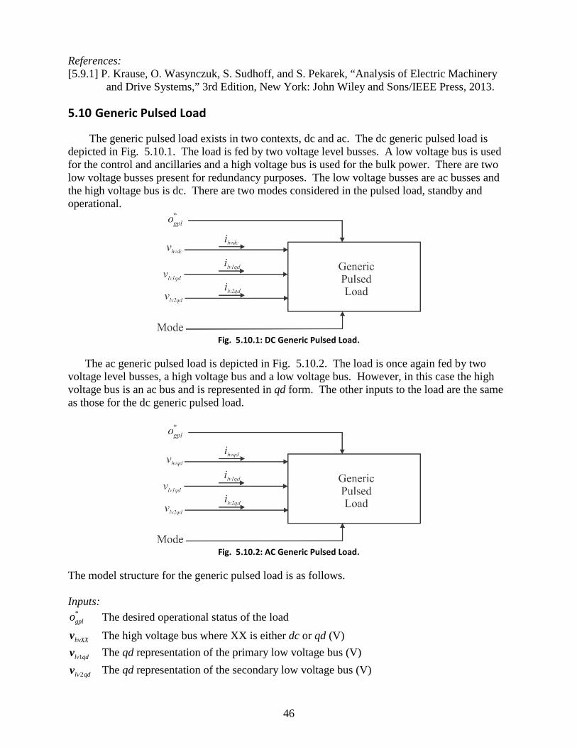
5.10 Generic Pulsed Load
The generic pulsed load exists in two contexts, dc and ac. The dc generic pulsed load is depicted in Fig. 5.10.1. The load is fed by two voltage level busses. A low voltage bus is used for the control and ancillaries and a high voltage bus is used for the bulk power. There are two low voltage busses present for redundancy purposes. The low voltage busses are ac busses and the high voltage bus is dc. There are two modes considered in the pulsed load, standby and operational.
Fig. 5.10.1: DC Generic Pulsed Load.
The ac generic pulsed load is depicted in Fig. 5.10.2. The load is once again fed by two voltage level busses, a high voltage bus and a low voltage bus. However, in this case the high voltage bus is an ac bus and is represented in qd form. The other inputs to the load are the same as those for the dc generic pulsed load.
Fig. 5.10.2: AC Generic Pulsed Load.
The model structure for the generic pulsed load is as follows. Inputs:
*gplo The desired operational status of the load
hvXXv The high voltage bus where XX is either dc or qd (V)
1lv qdv The qd representation of the primary low voltage bus (V)
2lv qdv The qd representation of the secondary low voltage bus (V)
47
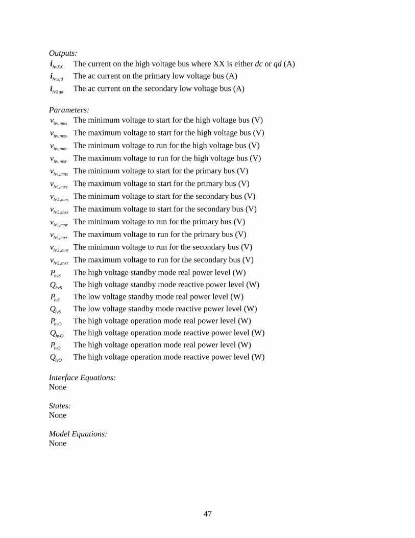
Outputs:
hvXXi The current on the high voltage bus where XX is either dc or qd (A)
1lv qdi The ac current on the primary low voltage bus (A)
2lv qdi The ac current on the secondary low voltage bus (A) Parameters:
hv,mnsv The minimum voltage to start for the high voltage bus (V)
hv,mxsv The maximum voltage to start for the high voltage bus (V)
hv,mnrv The minimum voltage to run for the high voltage bus (V)
hv,mxrv The maximum voltage to run for the high voltage bus (V)
1,lv mnsv The minimum voltage to start for the primary bus (V)
1,lv mxsv The maximum voltage to start for the primary bus (V)
2,lv mnsv The minimum voltage to start for the secondary bus (V)
2,lv mxsv The maximum voltage to start for the secondary bus (V)
1,lv mnrv The minimum voltage to run for the primary bus (V)
1,lv mxrv The maximum voltage to run for the primary bus (V)
2,lv mnrv The minimum voltage to run for the secondary bus (V)
2,lv mxrv The maximum voltage to run for the secondary bus (V)
hvSP The high voltage standby mode real power level (W)
hvSQ The high voltage standby mode reactive power level (W)
lvSP The low voltage standby mode real power level (W)
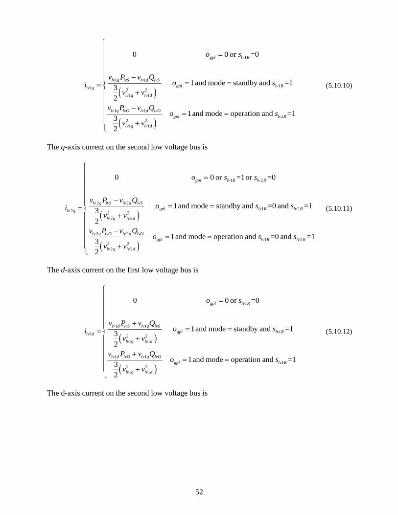
lvSQ The low voltage standby mode reactive power level (W)
hvOP The high voltage operation mode real power level (W)
hvOQ The high voltage operation mode reactive power level (W)
lvOP The high voltage operation mode real power level (W)
lvOQ The high voltage operation mode reactive power level (W) Interface Equations: None States: None Model Equations: None
48
5.10.1 DC Operation
For the dc application of the generic pulsed load, the high voltage bus is a dc bus where hvdcvis the dc voltage on the bus and hvdci is the dc current being drawn from the bus. The low voltage bus is represented in qd form as
lvXqlvXqd
lvXd
vv
=
v (5.10.1)
and
lvXqlvXqd
lvXd
ii
=
i (5.10.2)
where X can be either 1 or 2 depending on which low voltage bus being referred to.
The dc power for each bus is defined in Table 1. The values for these power levels are listed in the Nominal System Parameters section of the document.
Table 1: DC Operation
Mode Power Standby Operational
Phv PhvS PhvO Plv PlvS PlvO Qlv QlvS QlvO
5.10.2 AC Operation
In the ac application of the generic pulsed load the high voltage bus is an ac bus as well as the low voltage busses. In this case the high voltage bus, like the low voltage bus, is represented in qd form as
hvq
hvqdhvd
vv
v
=
(5.10.3)
and hvq
hvqdhvd
ii
i
=
(5.10.4)
The ac application of the generic pulsed load is similar to the dc operation, but also includes
the apparent power levels for the two modes for each bus. These power levels are listed in Table 2. The values for these power levels are listed in the Nominal System Parameters section of the document.
The supervisory control for the generic pulsed load is shown in Fig. 5.10.3. The inputs to the control are the desired operational status of the pulsed load, *
pdo , the measured high voltage bus level, hvmv , the measured first low voltage bus level, 1lv mv , and the measured second low voltage bus level, 2lv mv . The measured low voltage bus levels are obtained by
2 21
6lvXm lvXq lvXdv v v= + (5.10.5)
where X can be either 1 or 2 depending on which low voltage bus being referred to. The dc application high voltage measurement is equal to hvdcv , and the ac application high voltage bus measurement is obtained as
2 216hvm hvq hvdv v v= + (5.10.6)
50
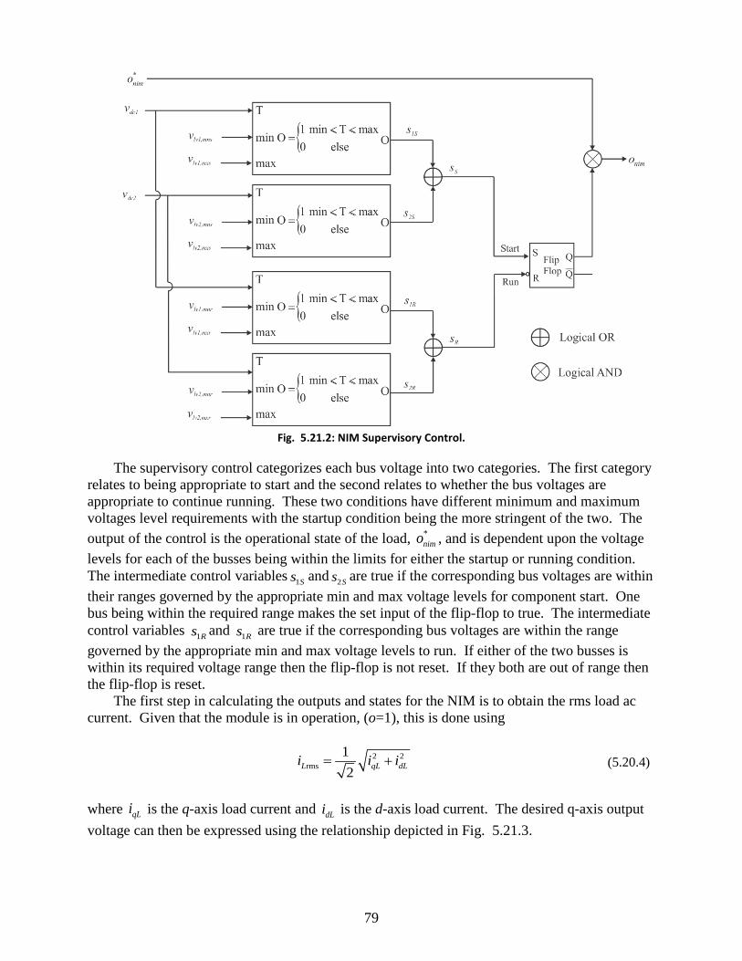
Fig. 5.10.3: GPL Supervisory Control.
There are two situations governed by the control. The first is during the startup condition and the second is during a running condition. These two conditions have different minimum and maximum voltage level requirements with the startup condition being the more stringent of the two. The output of the control is the operational state of the generic pulsed load and is dependent on the voltage levels for the three busses being within the limits for either the startup or running condition. The startup intermediate control variables hvSs , 1lv Ss , and 2lv Ss are true if the corresponding bus voltages are within their ranges governed by the appropriate min and max voltage levels. One of the low voltage busses must be within the required range and the high voltage bus must be within the required range in order for the operational state of the drive to be enabled. This same control scheme is used for the running condition which if not satisfied resets the operational state of the pulsed load.
51
5.10.4 Model Outputs
The outputs of the generic pulsed load are the currents for the three busses. For the dc application where the high voltage bus is dc, the high voltage bus current, hvi , is
0 0
1,mode standby
1,mode operational
gpl
hvShv gpl
hv
hvOgpl
hv
oPi ovP ov
=
= = =
= =
(5.10.7)
In the ac application of the pulsed load, the high voltage bus is an ac bus and therefore, the
q-axis current of the high voltage bus is
( )
( )
2 2
2 2
0 0
1, mode standby32
1, mode operation32
gpl
hvq hvS hvd hvSgplhvq
hvq hvd
hvq hvO hvd hvOgpl
hvq hvd
o
v P v Qoi
v v
v P v Qo
v v
= − = ==
+
−= =
+
(5.10.8)
and the d-axis current on the high voltage bus is
( )
( )
2 21 1
2 2
0 0
1, mode standby32
1, mode operation32
gpl
hvd hvS hvq hvSgplhvd
lv q lv d
hvd hvO hvq hvOgpl
hvq hvd
o
v P v Qoi
v v
v P v Qo
v v
= + = ==
+
+= =
+
(5.10.9)
Regardless of dc or ac application of the generic pulsed load, the low voltage bus is ac and
the q-axis current on the first low voltage bus is
52
( )
( )
1
1 111 2 2
1 1
1 11
2 21 1
0 0 or =0
1and mode standby and =132
1and mode operation and =132
gpl lv R
lv q lvS lv d lvSgpl lv Rlv q
lv q lv d
lv q lvO lv d lvOgpl lv R
lv q lv d
o s
v P v Qo si
v v
v P v Qo s
v v
= − = = =
+
−= =
+
(5.10.10)
The q-axis current on the second low voltage bus is
( )
( )
1 2
2 21 22 2 2
2 2
2 21 2
2 22 2
0 0 or =1or =0
1and mode standby and =0 and =132
1and mode operation and =0 and =132
gpl lv R lv R
lv q lvS lv d lvSgpl lv R lv Rlv q
lv q lv d
lv q lvO lv d lvOgpl lv R lv R
lv q lv d
o s s
v P v Qo s si
v v
v P v Qo s s
v v
=
−= = =
+
−= =
+
(5.10.11)
The d-axis current on the first low voltage bus is
( )
( )
1
1 111 2 2
1 1
1 11
2 21 1
0 0 or =0
1and mode standby and =132
1and mode operation and =132
gpl lv R
lv d lvS lv q lvSgpl lv Rlv d
lv q lv d
lv d lvO lv q lvOgpl lv R
lv q lv d
o s
v P v Qo si
v v
v P v Qo s
v v
= + = = =
+
+= =
+
(5.10.12)
The d-axis current on the second low voltage bus is
53
( )
( )
1 2
2 21 22 2 2
2 2
2 21 2
2 22 2
0 0 and =1and =0
1and mode standby and =0 and =132
1and mode operation and =0 and =32
gpl lv R lv R
lv d lvS lv q lvSgpl lv R lv Rlv d
lv q lv d
lv d lvO lv q lvOgpl lv R lv R
lv q lv d
o s s
v P v Qo s si
v v
v P v Qo s s
v v
=
+= = =
+
+= =
+1
(5.10.13)
If both of the low voltage busses are present and both hvi and hvi are high, then the first bus is
selected as the bus used to power the control and ancillaries of the GPL. Validation: The model is an abstraction of the requirement of a generic pulsed load (or constant power load) which consumes the desired power, but no internal dynamics are represented. References: None
5.11 Generic Hydrodynamic Load
The generic hydrodynamic load model is defined in [5.12.1-5.12.3] and outlined herein. The model structure is as follows.
Inputs:
propω Propeller angular frequency (rad/s) Outputs:
propT Counter torque exerted on shaft (Nm)
shipV Ship velocity (m/s) Parameters: ρ Density of salt water (kg/m3) D Propeller diameter (m)
rη Relative rotational efficiency (pu)
aV Propeller speed of advance (m/s) υ Modified advanced coefficient (pu)
( )QC υ Open water propeller torque coefficient function
( )Cτ υ Open water propeller thrust coefficient function
( )Tw shipV Taylor wake fraction
dT Thrust deduction factor
54
shipm Mass of ship (kg)
( )drag shipF V Hydrodynamic resistance (N vs knots) Interface equation: None States:
shipV Ship velocity (m/s) Model Equations: The model definition for the generic hydrodynamic load is given in [5.12.1] and outlined herein. First, the propeller speed of advance is found utilizing the Taylor Wake fraction as
( )( )T1 wa ship shipV V V= − (5.11.1)
Next, the thrust exerted on the ship is found using
2 2 2τC ( ) ( ( ) )(1 )ship a dF D V nD Tυ ρ= + − (5.11.2)
where
2propn
ωπ
= (5.11.3)
and
2 2( )a
nDV nD
υ =+
(5.11.4)
Next, the derivative of ship speed is found using
( )1 2 drag1 Fship
ship ship shipship
dVF F V
dt m = + − (5.11.5)
where 1shipF and 2shipF are the thrust exerted on the ship by propellers one and two. Finally, the counter torque on the propeller shaft is found using
32 2
QC ( ) ( ( ) )prop ar
DT V nDυ ρη
= +
(5.11.6)
Validation: The hydrodynamic represented here is general and valid for a given set of torque and thrust coefficients, and ship resistance, which all depend on various factors including propeller type, ship hull form, and operating conditions such as sea state conditions, and the presence of cavitation, for example. Further discussion and analysis of ship propulsion can be found in [5.12.4] and [5.12.5].
55
References: [5.12.1] E. J. Lecourt, Jr., “Using Simulation To Determine the Maneuvering Performance of the
WAGB-20,” Naval Engineer’s Journal, January 1998, pp. 171-188. [5.12.2] Syntek, “DD(X) Notional Baseline Modeling and Simulation Development Report,”
Internal Report, August 2003. [5.12.3] Robert F. Roddy, David E. Hess, and Will Faler, “Neural Network Predictions of the 4-
Quadrant Wageningen Propeller Series, NSWCCD-50-TR-2006/004, Naval Surface Warfare Center, Carderock Division, West Bethesda, MD, April 2006.
This section sets forth descriptions of the ac and dc line models. The dc line is a resistive line and the model structure is as follows. Inputs:
,dc xv The dc voltage at bus x (V)
,dc yv The dc voltage at bus y (V) Outputs:
,dc xyi The dc current through the line from bus x to bus y (A) Interface equation:
, , ,dc y dc x dc dc xyv v r i= − (5.12.1) States: None Model Equation:
, ,,
dc x dc ydc xy
dc
v vi
r−
= (5.12.2)
Validation: The chief sources of inaccuracy in this model are that temperature dependence and line inductance are neglected. This will cause the line model to tend to overestimate fault currents. References: None
56
5.12.2 AC Line
The ac line is an RL line and the model structure is as follows. Inputs:
,veqd x The vector of q- and d-axis voltages ( ,
eq xv and ,
ed xv ) at bus x of the line in the synchronous
ref. frame (V) ,ve
qd y The vector of q- and d-axis voltages ( ,eq yv and ,
ed yv ) at bus y of the line in the synchronous
ref. frame (V) eω The radian frequency of the synchronous reference frame (rad/s) Outputs:
,ieqd xy The q- and d-axis currents ( ,
eq xyi and ,
ed xyi ) through the line from bus x to bus y in the
synchronous ref. frame (A) Interface equation:
, , ,v v Z ie e e eqd y qd x qd qd xy= − (5.12.3)
where
eeqd
e
r LL r
ωω
= −
Z (5.12.4)
States: None Model Equations:
( ) ( )1
, , ,i Z v ve e e eqd xy qd qd x qd y
−= − (5.12.5)
Validation: This line model neglects temperature dependence. The line inductance is included, but only in a steady-state sense. Thus, fault current will tend to be overestimated. . In addition, it is assumed that the line is balanced and symmetrical. References: None
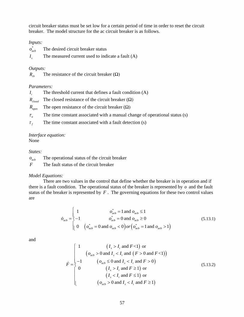
5.13 AC Circuit Breaker Model
The ac circuit breaker model represents the opening and closing of the breaker as a change
in resistance. This is done in such a way as to avoid discontinuities. The breaker either opens due to the measured current being greater than a threshold indicating a fault, or if the desired circuit breaker status ( *
acbo ) is open. If the breaker trips due to an over-current, the desired
57
circuit breaker status must be set low for a certain period of time in order to reset the circuit breaker. The model structure for the ac circuit breaker is as follows. Inputs:
*acbo The desired circuit breaker status
sI The measured current used to indicate a fault (A) Outputs:
cbR The resistance of the circuit breaker (Ω) Parameters:
tI The threshold current that defines a fault condition (A)
closedR The closed resistance of the circuit breaker (Ω)
openR The open resistance of the circuit breaker (Ω)
oτ The time constant associated with a manual change of operational status (s)
fτ The time constant associated with a fault detection (s) Interface equation: None States:
acbo The operational status of the circuit breaker F The fault status of the circuit breaker Model Equations: There are two values in the control that define whether the breaker is in operation and if there is a fault condition. The operational status of the breaker is represented by o and the fault status of the breaker is represented by F . The governing equations for these two control values are
( ) ( )
*
*
* *
1 1and 11 0 and 0
0 0 and 0 1and 1
acb acb
acb acb acb
acb acb acb acb
o oo o o
o o or o o
= ≤= − = ≥ = < = >
(5.13.1)
and
( )( )( )
( )( )( )
( )
1 and <1 or0 and and 0 and <1
1 0 and and 00 and 1 or
and 1 or0 and and 1
s t
acb s t
acb s t
s t
s t
acb s t
I I Fo I I F F
o I I FFI I FI I F
o I I F
> > < > − ≤ < >=
> ≥ < ≤
> < ≥
(5.13.2)
58
The derivatives of the control signals are then calculated as
1acbacb
o
do odt τ
= (5.13.3)
1
F
dF Fdt τ
= (5.13.4)
The status of the circuit breaker (open/closed) is then governed by
min( ,1 )acbc o F= − (5.13.5) and the resistance of the circuit breaker is
( ) ( )( )max max minlog( ) log log10 R c R RR − −= (5.13.6) Validation:
It must be recognized that this model is completely behavioral in nature. Functionally, it will operate as a circuit breaker and interrupt a fault current and be re-closable. However, the dynamics of the circuit breaker are not based on physics and so the model does not correctly portray the short-time scale behavior of circuit breaker operation. References: None
5.14 Transformer
The q and d-axis equivalent circuits for the transformer model are depicted in Fig. 5.14.1 and Fig. 5.14.2.
The equivalent resistance ( eqr ) and inductance ( eqL ) are found using
'eq p sr r r= + (5.14.1)
'
,l eq lp lsL L L= + (5.14.2) The model structure is as follows.
Inputs: ,p qdv The primary side voltage in the qd reference frame (V)
,s qdi The secondary side current in the qd reference frame (A)
eω The electrical speed of the synchronous reference frame (rad/s) Outputs:
,s qdv The secondary side voltage in the qd reference frame (V)
,p qdi The primary side current in the qd reference frame (A) Parameters:
pr The primary side winding resistance (Ω) '
sr The secondary side winding resistance referred to the primary side (Ω)
lpL The primary side winding leakage inductance (H) '
l sL The secondary side winding leakage inductance referred to the primary side (H)
pN The number of turns on the primary winding
sN The number of turns on the secondary winding Interface Equations:
',pq eq pq e l eq pd sqv r i L i vω= + + (5.14.3)
'
,pd eq pd e l eq pq sdv r i L i vω= − + (5.14.4)
60
States: None Model Equations: The relationship between the referred and non-referred quantities is
' psX sX
s
Nv v
N= (5.14.5)
and
' ssX sX
p
Ni iN
= (5.14.6)
where X can either be q or d.
'sX pXi i= (5.14.7)
Lastly, the resistance and inductance are referred using
2' p
s ss
Nr r
N
=
(5.14.8)
and 2
' pls l s
s
NL L
N
=
(5.14.9)
Validation: The model described assumes a balanced three phase transformer. The magnetizing inductance is assumed to be infinite, and the leakage saturation and temperature effects are ignored. Since this is a reduced-order model, initial fault currents will tend to be over-predicted. References: None
5.15 Zonal Active Rectifier
The Zonal Active Rectifier is depicted in Fig. 5.15.1.
61
Fig. 5.15.1: Zonal Active Rectifier.
The model structure for the Zonal Active Rectifier is as follows. Inputs:
,in qdv The ac side voltage in the qd reference frame (V)
,out dci The dc output current (A) *zaro The desired status of the component
Outputs:
,in qdi The ac side current in the qd reference frame (A)
,out dcv The dc output voltage (V) Parameters:
dr The droop resistance (Ω) *outv The desired no load output voltage (V)
ti The fault current threshold (A)
fi The peak fault current (A) Interface Equations: None States: None Model Equations: The supervisory control for the Zonal Active Rectifier is shown in Fig. 5.15.2. The inputs to the control are the measured voltage level of the bus and the desired operational status of the load, *
zaro . The output of the supervisory control is the operational state of the load, zaro . The supervisory control categorizes the bus voltage into two categories. The first category relates to being appropriate to start and the second relates to whether the bus voltage is appropriate to continue running. These two conditions have different minimum and maximum voltages level requirements with the startup condition being the more stringent of the two. The output of the control is the operational state of the load, *
zaro , and is dependent upon the voltage
62
levels of the buss being within the limits for either the startup or running condition. The intermediate control variables SS and RS are true if the bus voltage is within the ranges governed by the appropriate min and max voltage levels for component start or run. If the bus is within its required voltage range then the flip-flop is not reset. If it is out of range then the flip-flop is reset.
Fig. 5.15.2: Zonal Active Rectifier Supervisory Control.
The dc output voltage of the rectifier as a function of output current is depicted in Fig. 5.15.3.
Fig. 5.15.3: Zonal Active Rectifier Output Voltage.
The output voltage is therefore expressed
63
*
0 0 or 1and 1and
zar out f
out out d out zar out t
out zar out t
o i iv v r i o i i
mi c o i i
= >= − = < + = ≥
(5.15.1)
where
*d t out
f t
r i vmi i
−=
− (5.15.2)
and
( )*out d t f
f t
v r i ic
i i−
=−
(5.15.3)
The output power is found using
out out outP v i= (5.15.4) and the input power is found using
outin nl
inc
PP Pη
= + (5.15.5)
where
outinc
in
PP
η ∆=
∆ (5.15.6)
is the incremental efficiency. The q and d-axis currents can then be calculated using
2 2
23 in q
qq d
P vi
v v=
+ (5.15.7)
and
2 2
23 in d
dq d
P vi
v v=
+ (5.15.8)
Validation: The behavior of this component is based on what is possible in terms of power balance. It is an abstraction of a desired component performance. References: None
64
5.16 Type 1 DC Load
The Type 1 dc load is depicted in Fig. 5.16.1 and is a resistive load fed by one of two busses. The first input bus is the primary power source and the second bus supplies backup power.
Fig. 5.16.1: Zonal DC Load.
The model structure is defined as follows. Inputs:
*1dco The desired operational status of the load
1dcv The dc voltage on the primary bus (V)
2dcv The dc voltage on the secondary bus (V) Outputs:
1dci The dc current on the primary bus (A)
2dci The dc current on the secondary bus (A) Parameters:
1,lv mnsv The minimum voltage to start for the primary bus (V)
1,lv mxsv The maximum voltage to start for the primary bus (V)
2,lv mnsv The minimum voltage to start for the secondary bus (V)
2,lv mxsv The maximum voltage to start for the secondary bus (V)
1,lv mnrv The minimum voltage to run for the primary bus (V)
1,lv mxrv The maximum voltage to run for the primary bus (V)
2,lv mnrv The minimum voltage to run for the secondary bus (V)
2,lv mxrv The maximum voltage to run for the secondary bus (V)
dcr The resistance of the dc load (Ω) Interface Equations: None States: None Model Equations:
65
The supervisory control for the load is depicted in Fig. 5.16.2. The inputs to the supervisory control are the measured dc voltages on each of the two busses, 1dc mv and 2dc mv , and the desired operational status of the load, *
1dco .
Fig. 5.16.2: Zonal DC Load Supervisory Control.
The supervisory control categorizes each bus voltage into two categories. The first category relates to being appropriate to start and the second relates to whether the bus voltages are appropriate to continue running. These two conditions have different minimum and maximum voltages level requirements with the startup condition being the more stringent of the two. The output of the control is the operational state of the load, *
1dco , and is dependent upon the voltage levels for each of the busses being within the limits for either the startup or running condition. The intermediate control variables 1Ss and 2Ss are true if the corresponding bus voltages are within their ranges governed by the appropriate min and max voltage levels for component start. One bus being within the required range makes the set input of the flip-flop to true. The intermediate control variables 1Rs and 1Rs are true if the corresponding bus voltages are within the range governed by the appropriate min and max voltage levels to run. If either of the two busses is within its required voltage range then the flip-flop is not reset. If they both are out of range then the flip-flop is reset.
The output of the dc load model are the two load currents, 1dci and 2dci , which are given by
1 1
1 11 1
0 0 or 0
1and s 1
dc R
dc dcdc R
dc
o si v o
r
= == = =
(5.16.1)
66
1 2
2 21 1
0 0 or 0
1and 0
dc R
dc dcdc R
dc
o si v o s
r
= = = = =
(5.16.2)
Validation: The behavior of this component is based on what is possible in terms of power balance. It is an abstraction of a desired component performance. References: None
5.17 Type 2 DC Load
The type 2 dc load is the same configuration as the Type 1 dc load depicted in Fig. 5.16.1, but represents a constant power load. The model structure for this load is identical to that of the Type 1 dc load. The supervisory control for the load is identical to that of the Type 1 dc load depicted in Fig. 5.16.2 with the output being 2dco instead of 1dco .
The outputs of the Type 2 dc load model are the two load currents, 1dci and 2dci , which are given by
2 1
12 1
1
0 0 or 0
1and s 1
dc R
dc dcdc R
dc
o si P o
v
= == = =
(5.17.1)
2 2
22 1
2
0 0 or 0
1and 0
dc R
dc dcdc R
dc
o si P o s
v
= = = = =
(5.17.2)
5.18 AC Load
The ac load is an RL load fed by two ac busses and is depicted in Fig. 5.18.1. The first input bus is the primary power source and the second bus supplies backup power.
Fig. 5.18.1: Zonal AC Load.
The model structure is defined as follows.
67
Inputs: *aco The desired operational status of the load
1qdv The ac voltage on the primary bus (V)
2qdv The ac voltage on the secondary bus (V)
eω The electrical speed of the synchronous reference frame (rad/s) Outputs:
1qdi The ac current on the primary bus (A)
2qdi The ac current on the secondary bus (A) Parameters:
1,ac mnsv The minimum voltage to start for the primary bus (V)
1,ac mxsv The maximum voltage to start for the primary bus (V)
2,ac mnsv The minimum voltage to start for the secondary bus (V)
2,ac mxsv The maximum voltage to start for the secondary bus (V)
1,ac mnrv The minimum voltage to run for the primary bus (V)
1,ac mxrv The maximum voltage to run for the primary bus (V)
2,ac mnrv The minimum voltage to run for the secondary bus (V)
2,ac mxrv The maximum voltage to run for the secondary bus (V)
acr The resistance of the ac load (Ω)
acL The inductance of the ac load (Ω) Interface Equations: None States: None Model Equations:
The supervisory control for the ac load is depicted in Fig. 5.18.2. The inputs to the control
are the measured voltage levels for each of the busses and the desired operational status of the load, *
aco . The output of the supervisory control is the operational state of the load, aco .
68
Fig. 5.18.2: Zonal AC Load Supervisory Control.
The measured voltage levels for the two busses are found using
2 216acXm qX dXv v v= + (5.18.1)
where X can either be 1 or 2.
The supervisory control categorizes each bus voltage into two categories. The first category relates to being appropriate to start and the second relates to whether the bus voltages are appropriate to continue running. These two conditions have different minimum and maximum voltages level requirements with the startup condition being the more stringent of the two. The output of the control is the operational state of the load, *
aco , and is dependent upon the voltage levels for each of the busses being within the limits for either the startup or running condition. The intermediate control variables 1Ss and 2Ss are true if the corresponding bus voltages are within their ranges governed by the appropriate min and max voltage levels for component start. One bus being within the required range makes the set input of the flip-flop to true. The intermediate control variables 1Rs and 1Rs are true if the corresponding bus voltages are within the range governed by the appropriate min and max voltage levels to run. If either of the two busses is within its required voltage range then the flip-flop is not reset. If they both are out of range then the flip-flop is reset.
The model outputs for the ac load are the q and d axis currents for each of the busses, 1qi ,
1di , 2qi and 2di , which are computed as
69
1
1 1112 2 2
0 0 or 0
1and s 1
ac ac R
ac q ac dqac ac R
ac ac
o sr v L vi
or L
ωω
= = −= = = +
(5.18.2)
1
1 1112 2 2
0 0 or 0
1and s 1
ac ac R
ac d ac qdac ac R
ac ac
o sr v L vi
or L
ωω
= = += = = +
(5.18.3)
2
2 2212 2 2
0 0 or 0
1and s 0
ac ac R
ac q ac dqac ac R
ac ac
o sr v L vi
or L
ωω
= = −= = = +
(5.18.4)
2
2 2212 2 2
0 0 or 0
1and s 0
ac ac R
ac d ac qdac ac R
ac ac
o sr v L vi
or L
ωω
= = += = = +
(5.18.5)
Validation:
This component model is an exact steady-state model of a balanced RL load, neglecting temperature variations. It does not include dynamics. References: None
5.19 Isolated DC-DC Converter
The IDCDC converter considered herein is an isolated, peak-current controlled, uni-directional DC-DC converter [5.21.1]. The topology is shown in Fig. 5.19.1. The control of the DC-DC converter is shown in Fig. 5.19.2. A simplified equivalent circuit used to derive the average value model (AVM) is seen in Fig. 5.19.3.
70
Fig. 5.19.1: DC-DC Converter Topology.
Fig. 5.19.2: DC-DC Converter Control.
71
Fig. 5.19.3: AVM Simplified Topology.
The average value model of the IDCDC converter is as follows: Inputs:
*v The commanded output filter capacitor voltage (V) ifv The input voltage of the DC-DC converter (V)
ldi The load current drawn from the DC-DC converter (A) Outputs:
ifi The current drawn by the DC-DC converter (A)
ofv Output filter capacitor voltage (V) Parameters:
pcmL Input filter inductance (H)
pcmr Input filter inductor’s resistance (Ω)
pcmC Input filter capacitance (F)
mL Transformer magnetizing inductance (H)
lpL Transformer primary leakage inductance (H)
lpr Transformer primary leakage resistance (Ω)
lsL Transformer secondary leakage inductance (H)
lsr Transformer secondary leakage resistance (Ω)
1
2
NN
Transformer turns ratio (no units)
recL DC link inductance (H)
recr Resistance of DC link inductor (Ω)
72
scmL Output filter inductance (H)
scmr Output filter inductor’s resistance (Ω)
scmC Output filter capacitance (F)
pK Proportional constant (Ω-1)
iK Integral constant ((Ωs)-1)
dK Droop constant (Ω)
_pmax uli Upper limit of maximum transformer primary current (A)
_pmax lli Lower limit of maximum transformer primary current (A)
swf Switching frequency of transformer (Hz)
swT Time period of switching of transformer (s)
slrτ Slew rate limit constant (s)
awuτ Anti-windup constant (s) **minv Minimum rate of change of voltage command (Vs-1) **maxv Minimum rate of change of voltage command (Vs-1)
,in mnsv Minimum voltage required at input to enable operation (V)
,in mxsv Maximum voltage allowed at input to enable operation (V)
,in mnrv Minimum voltage required to remain operational (V)
,in mxrv Maximum voltage allowed to remain operational (V) Interface Equations: None States:
**v The slew-rate limited voltage command (control) (V) PII Integral term in the PI control (A)
ofv Output filter capacitor voltage (V) Model Equations:
A supervisory control which turns the DC-DC converter on only if the input voltage is within as certain range of voltage and turns the DC-DC converter off if the input voltage is out outside of another range of voltage has also been implemented apart from the main peak-current control. This can be seen in Fig. 5.19.4.
73
Fig. 5.19.4: Supervisory Control of the DC-DC Converter.
This supervisory control gives as output, idcdco , which is 1 if the DC-DC converter is operational and 0 if the DC-DC converter is non-operational.
First, the equations that determine the derivative of the states are presented. A variable, **v is defined as follows.
* ****
slr
v vvτ−
= (5.19.1)
where slrτ is the slew-rate limit time constant. The time derivative of the slew-rate limited voltage command is obtained as
** ** ** **
** ** ** **
** ** **
ififif
min max
max max
min min
v v v vd v v v vdt
v v v
< <= > <
(5.19.2)
The PI control with droop is detailed below:
( )**e idcdc ofd ldv o vv K i= −− (5.19.3)
where dk is the droop constant and ldi is the load current. The proportional part of the control is obtained as:
PI p eP K v= (5.19.4) The integral part of the control is obtained from
( ) ( ) idcdcPI i e idcdc i PI AWUd I K v o K I o Idt
= + − + (5.19.5)
74
( )pmax idcdcPI PIi oP I= + (5.19.6)
wherein AWUI is anti-windup, which is zero as long as the output of the control, pmaxi , is within the prescribed limits. If pmaxi is outside the prescribed limits, then the anti-windup can be defined as
_
__
( )
( )
i pmax ul pmaxpmax pmax_ul
awuAWU
i pmax ll pmaxpmax pmax ll
awu
K i ii i
IK i i
i i
τ
τ
−>
= − <
(5.19.7)
The time derivative of the output filter capacitor voltage, ofv is obtained as
of ldof
scm
i id vdt C
−= (5.19.8)
The output filter capacitor voltage, ofv is a state and an output. Thus, based on the equations presented above, the only two quantities that need to be derived are ofi and ifi . These are obtained based on approximating the transformer primary and secondary current waveforms. These are presented in Fig. 5.19.5.
Fig. 5.19.5: Transformer Primary and Secondary Current Waveforms.
75
The following constants are first described:
1
2
NKN
= (5.19.9)
( )
( ) ( )2
1 2 2
m m ls rec
m lplp ls rec ls rec
L L L K LC
L LL L K L L K L+ +
=++ + +
(5.19.10)
( )
( ) ( )2 2 2
m lpm
m lplp ls rec ls rec
L LLC
L LL L K L L K L
+=
++ + + (5.19.11)
The time in each of the regions: 1t , 2t and 3t , and 2i can be obtained as follows:
( )( )
( )
21
pmax
m lsif
lp ls m lp ls
i it
L Lv
L L L L L
+=
++ +
(5.19.12)
2
2
2of
rec
if of of
m lp m rec
v TswKLt
v Kv vC
L L L KL
=
− + +
(5.19.13)
3 1 22swTt t t= − − (5.19.14)
where
2 1 2 2if of
pmaxm m ls rec
v Kvi i C t
L L L K L
−= − + + (5.19.15)
Using these expressions, ofi and ifi are obtained as follows:
( )11
2if m
oflp ls m lp ls
Kv L ti
L L L L L=
+ + (5.19.16)
2 2
1 22 2
2
pmax pmax
ifsw
i i i it ti T
− + + + = (5.19.17)
Thus, the complete model has been defined.
Validation:
76
This model is a highly simplified version of the model set forth in [5.21.1]. Although some studies using the model have been compared to detailed waveform level models, and these comparisons have been generally favorable, the model must be viewed as relatively immature. References: [5.21.1] Suryanarayana, H.; Sudhoff, S.D., "Average-value modeling of a peak-current
controlled galvanically-isolated DC-DC converter for shipboard power distribution," Electric Ship Technologies Symposium (ESTS), 2013 IEEE , vol., no., pp.152,161, 22-24 April 2013.
5.20 DC Fault Detection Unit
The dc fault detection unit consists of a low voltage dc source connected to the DC bus. The unit is depicted in Fig. 5.20.1. This source is used to detect if a fault on the dc bus has been cleared such that the system can be brought back online.
Fig. 5.20.1: DC Fault Detection Unit.
During non-fault operation, there is no current sourced from the fault detection supply due to the series diode. When a fault occurs, the dc voltage of the bus collapses due to fault detection features of the dc bus source. The dc bus will stay at zero as long as the fault is present. Once the fault is cleared, the bus voltage will rise above a threshold defined by the fault detection unit supply voltage. This is an indication to the system that the fault has been cleared and the system can be brought back online. The model structure for the fault detection unit is as follows. Inputs:
dcv The dc voltage on the bus prior to the unit (V)
outi The dc current on the bus after the unit (A) Outputs:
outv The dc voltage on the bus after the unit (V)
dci The dc current in the bus prior to the unit (A) F The fault status of the system Parameters:
fduv The voltage level of the unit (V)
77
fdur The resistance of the unit (Ω) Interface Equations:
0 dc fdu
fdu dcfdudc fdu
fdu
v vv vi
v vr
≥ −= <
(5.20.1)
dc out fdui i i= − (5.20.2)
States: None Model Equations: The fault status is determined by the voltage level of the bus. If the bus voltage, outv , is less than the voltage level of the detection unit, then there is a fault on the system as the unit is unable to raise the bus voltage above the threshold. Therefore,
01
out fdu
out fdu
v vF
v v>=
= < (5.20.3)
Validation: This component could certainly be used and implemented in a power system, if desired. References: None
5.21 Non-Isolated Inverter Module
The Non-Isolated Inverter Module model is depicted in Fig. 5.21.1.
Fig. 5.21.1: Non-Isolated Inverter Module.
The component model structure is as follows. Inputs:
78
1dcv The dc voltage of the primary bus (V)
2dcv The dc voltage of the secondary bus (V)
qLi The q-axis load current (A)
dLi The d-axis load current (A) *nimo The desired operational status of the component
Outputs:
1dci The dc current drawn from the primary bus (A)
2dci The dc current drawn from the secondary bus (A)
qLv The q-axis voltage on the load side (V)
2dci The d-axis voltage on the load side (V)
outP The output power of the component (W) Parameters:
Lti The threshold level load current (A)
Lfi The fault level load current (A) C The capacitance of the dc bus (F) τ The time constant associated with the bus capacitance (s)
*qv The desired q-axis output voltage (V)
eω The electrical speed of the synchronous reference frame (rad/s) *LLv The desired line-line output voltage (V)
Interface Equations: None States:
qv The q-axis output voltage (V)
dv The d-axis output voltage (V) Model Equations:
The supervisory control for the NIM is depicted in Fig. 5.21.2. The inputs to the supervisory control are the measured dc voltages on each of the two busses, 1dcv and 2dcv , and the desired operational status of the load, *
nimo .
79
Fig. 5.21.2: NIM Supervisory Control.
The supervisory control categorizes each bus voltage into two categories. The first category relates to being appropriate to start and the second relates to whether the bus voltages are appropriate to continue running. These two conditions have different minimum and maximum voltages level requirements with the startup condition being the more stringent of the two. The output of the control is the operational state of the load, *
nimo , and is dependent upon the voltage levels for each of the busses being within the limits for either the startup or running condition. The intermediate control variables 1Ss and 2Ss are true if the corresponding bus voltages are within their ranges governed by the appropriate min and max voltage levels for component start. One bus being within the required range makes the set input of the flip-flop to true. The intermediate control variables 1Rs and 1Rs are true if the corresponding bus voltages are within the range governed by the appropriate min and max voltage levels to run. If either of the two busses is within its required voltage range then the flip-flop is not reset. If they both are out of range then the flip-flop is reset.
The first step in calculating the outputs and states for the NIM is to obtain the rms load ac current. Given that the module is in operation, (o=1), this is done using
2 2
rms12L qL dLi i i= + (5.20.4)
where qLi is the q-axis load current and dLi is the d-axis load current. The desired q-axis output voltage can then be expressed using the relationship depicted in Fig. 5.21.3.
80
Fig. 5.21.3: NIM q-axis Voltage.
In the above figure, the desired q-axis voltage is a constant determined by the desired line-line voltage until the rms load current reaches a threshold value where it ramps to zero before the load current can reach the fault threshold. The desired d-axis voltage is zero. Once the desired q-axis voltage is determined, the raw q and d axis currents are calculated using
( )*qir qL e d q q
Ci i Cv v vωτ
= + + − (5.20.5)
and
( )dir dL e q dCi i Cv vωτ
= − − (5.20.6)
where qv and dv are the states of the NIM. The rms raw inverter current is then calculated as
2 212mir qir diri i i= + (5.20.7)
If the raw rms inverter current, miri , is less than the threshold load current, Lti , then
qi qiri i= (5.20.8) and
di diri i= (5.20.9)
Otherwise,
2mir
qi qirLf
ii ii
=
(5.20.10)
and
2mir
di dirLf
ii ii
=
(5.20.11)
81
The states of the NIM are obtained from
1qqi qL e d
dvi i Cv
dt Cω = − − (5.20.12)
and
1d
di dL e qdv i i Cvdt C
ω = − + (5.20.13)
The output power is obtained from
( )32out q qi d diP v i v i= + (5.20.14)
and the dc current drawn by the NIM from the bus is
1
11
1
0 0 or 0
1and s 1
nim R
dc outnim R
dc
o si P o
v
= == = =
(5.20.15)
2
22
2
0 0 or 0
1and s 1
nim R
dc outnim R
dc
o si P o
v
= == = =
(5.20.16)
Validation: This is a very simple model of the desired behavior of an inverter module. The degree to which it holds is a function of the specific converter design. References: None