© IMEC 2010
EUV resist material performance, progress and process improvements at imecA.M. Goethals, A. Niroomand1, K. Ban2, K. Hosokawa,
F. Van Roey, I. Pollentier, C. Jehoul, D. Van den Heuvel
and K. Ronse
IMEC, Leuven, Belgium
On assignment from 1Micron, 2Hynix, 3Elpida
International EUVL Symposium, 17- 20 Oct 2010, Kobe
© IMEC 2010
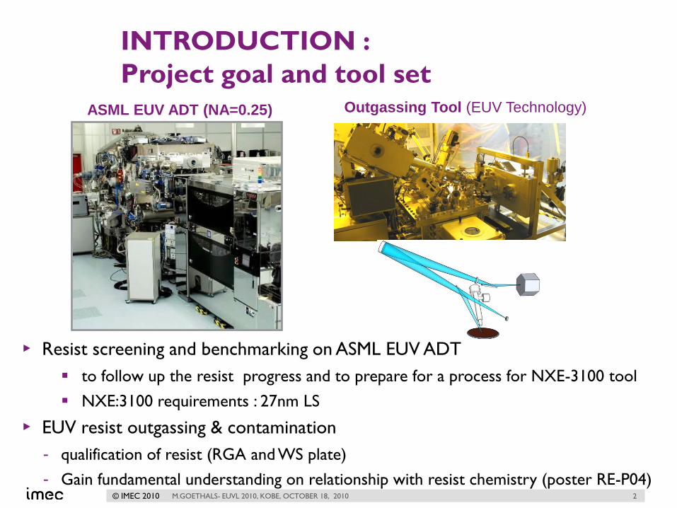
INTRODUCTION :
Project goal and tool set
▸ Resist screening and benchmarking on ASML EUV ADT
to follow up the resist progress and to prepare for a process for NXE-3100 tool
NXE:3100 requirements : 27nm LS
▸ EUV resist outgassing & contamination
- qualification of resist (RGA and WS plate)
- Gain fundamental understanding on relationship with resist chemistry (poster RE-P04)M.GOETHALS- EUVL 2010, KOBE, OCTOBER 18, 2010 2
Outgassing Tool (EUV Technology)ASML EUV ADT (NA=0.25)
© IMEC 2010
OUTGASSING : PAG TYPE
M.GOETHALS- EUVL 2010, KOBE, OCTOBER 18, 2010 3
Polymer
diffusion limited
Cation size
limited
cation
PAG
Several PAG cations are tested
towards WS contamination
Both small PAG cations as
well as very heavy PAG
cations give lower WS
contamination, however it is
expected that for S-
containing cations the high-
MW will result in less non-
cleanable contamination
Poster RE-P04
I. Pollentier
© IMEC 2010
OUTLINE
Introduction
Lithographic screening▸ Resist screening
▸ Underlayer screening
Benchmarking ▸ Lithographic performance
▸ Process defectivity
Process improvements▸ TBAH
▸ FIRM
M.GOETHALS- EUVL 2010, KOBE, OCTOBER 18, 2010 4
© IMEC 2010 5
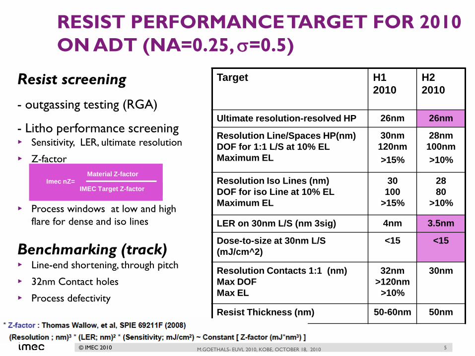
RESIST PERFORMANCE TARGET FOR 2010
ON ADT (NA=0.25, s=0.5)
Target H1
2010
H2
2010
Ultimate resolution-resolved HP 26nm 26nm
Resolution Line/Spaces HP(nm)
DOF for 1:1 L/S at 10% EL
Maximum EL
30nm
120nm
>15%
28nm
100nm
>10%
Resolution Iso Lines (nm)
DOF for iso Line at 10% EL
Maximum EL
30
100
>15%
28
80
>10%
LER on 30nm L/S (nm 3sig) 4nm 3.5nm
Dose-to-size at 30nm L/S
(mJ/cm^2)
<15 <15
Resolution Contacts 1:1 (nm)
Max DOF
Max EL
32nm
>120nm
>10%
30nm
Resist Thickness (nm) 50-60nm 50nm
M.GOETHALS- EUVL 2010, KOBE, OCTOBER 18, 2010
Resist screening
- outgassing testing (RGA)
- Litho performance screening▸ Sensitivity, LER, ultimate resolution
▸ Z-factor
▸ Process windows at low and high
flare for dense and iso lines
Benchmarking (track)▸ Line-end shortening, through pitch
▸ 32nm Contact holes
▸ Process defectivity
Imec nZ=Material Z-factor
IMEC Target Z-factor
© IMEC 2010
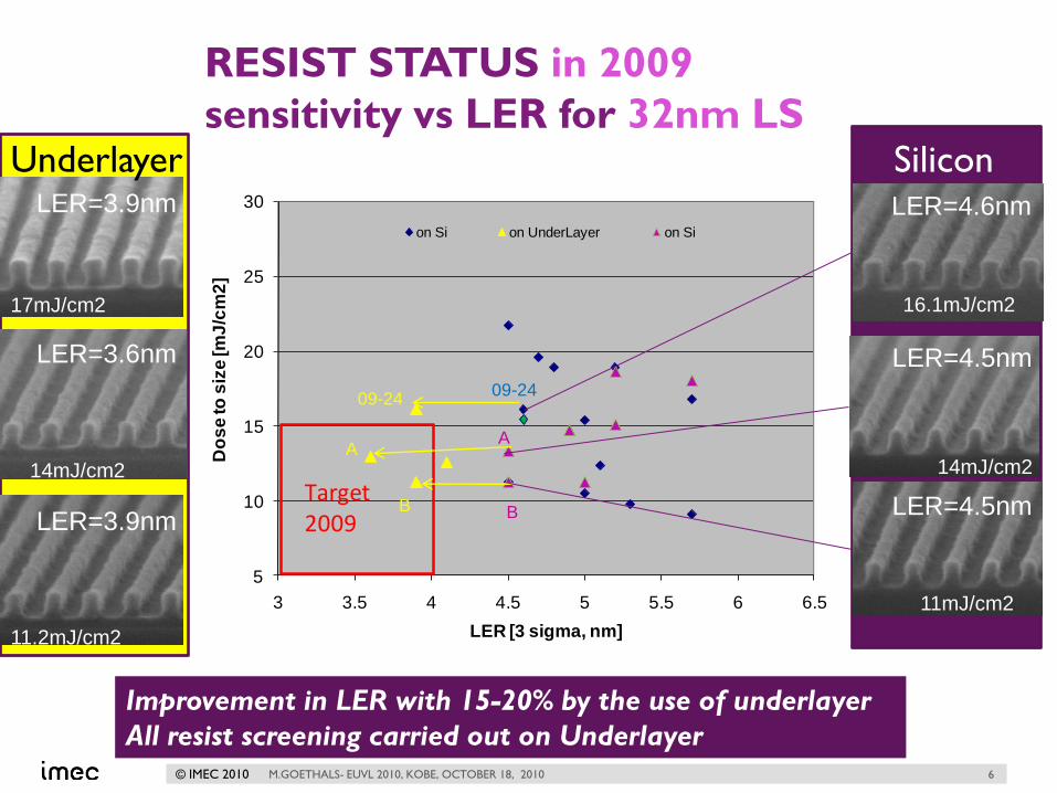
5
10
15
20
25
30
3 3.5 4 4.5 5 5.5 6 6.5
Do
se
to
siz
e [m
J/c
m2
]
LER [3 sigma, nm]
on Si on UnderLayer on Si
Target2009
RESIST STATUS in 2009
sensitivity vs LER for 32nm LS
M.GOETHALS- EUVL 2010, KOBE, OCTOBER 18, 2010 6
B
A
09-24
A
B
Improvement in LER with 15-20% by the use of underlayer
All resist screening carried out on Underlayer
LER=4.6nm
16.1mJ/cm2
14mJ/cm2
LER=4.5nm
11mJ/cm2
LER=4.5nm
Silicon LER=3.9nm
17mJ/cm2
14mJ/cm2
LER=3.6nm
11.2mJ/cm2
LER=3.9nm
Underlayer
09-24
© IMEC 2010
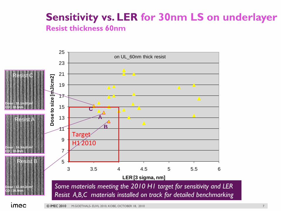
Sensitivity vs. LER for 30nm LS on underlayerResist thickness 60nm
M.GOETHALS- EUVL 2010, KOBE, OCTOBER 18, 2010 7
5
7
9
11
13
15
17
19
21
23
25
3 3.5 4 4.5 5 5.5 6
Do
se
to
siz
e [m
J/c
m2
]
LER [3 sigma, nm]
on UL_60nm thick resist
TargetH1 2010
B
A
C
Some materials meeting the 2010 H1 target for sensitivity and LER
Resist A,B,C materials installed on track for detailed benchmarking
Dose : 15.1mJ/cm2
CD : 30.5nm
Resist C
Dose : 14.3mJ/cm2
CD : 30.4nm
Resist A
Dose : 12.4mJ/cm2
CD : 30.4nm
Resist B
© IMEC 2010
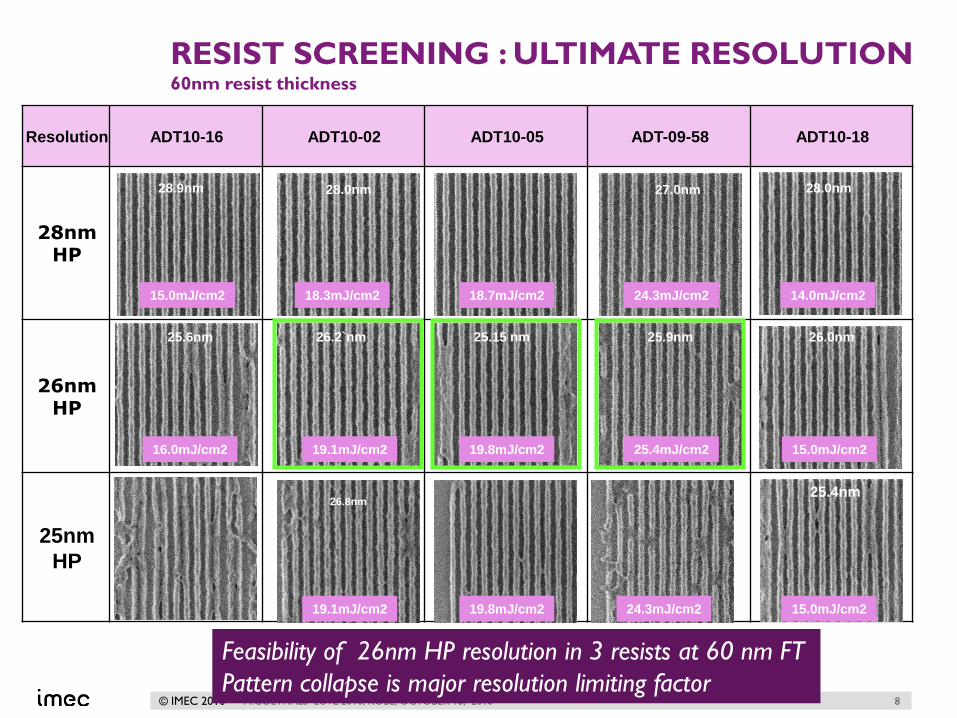
Resolution ADT10-16 ADT10-02 ADT10-05 ADT-09-58 ADT10-18
28nm HP
26nm HP
25nm
HP
RESIST SCREENING : ULTIMATE RESOLUTION60nm resist thickness
M.GOETHALS- EUVL 2010, KOBE, OCTOBER 18, 2010 8
18.7mJ/cm2
19.8mJ/cm2
19.8mJ/cm2
25.15 nm
27.0nm
24.3mJ/cm2
25.9nm
25.4mJ/cm2
24.3mJ/cm2
18.3mJ/cm2
28.0nm
26.2`nm
19.1mJ/cm2
26.8nm
19.1mJ/cm2
26.4nm
26.nm
27.2nm
2.
14.0mJ/cm2
15.0mJ/cm2
28.0nm
26.0nm
25.4nm
15.0mJ/cm2
28.9nm
15.0mJ/cm2
25.6nm
16.0mJ/cm2
Feasibility of 26nm HP resolution in 3 resists at 60 nm FT
Pattern collapse is major resolution limiting factor
© IMEC 2010
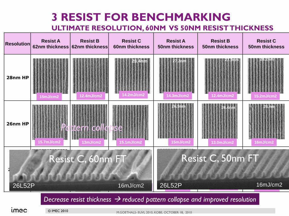
ResolutionResist A
62nm thickness
Resist B
62nm thickness
Resist C
60nm thickness
Resist A
50nm thickness
Resist B
50nm thickness
Resist C
50nm thickness
28nm HP
26nm HP
25nm HP
3 RESIST FOR BENCHMARKINGULTIMATE RESOLUTION, 60NM VS 50NM RESIST THICKNESS
M.GOETHALS- EUVL 2010, KOBE, OCTOBER 18, 2010
9
26.nm
28.4nm
14.2mJ/cm2
15.1mJ/cm2
15.1mJ/cm2
15mJ/cm2
15.7mJ/cm2
15.7mJ/cm2
12.4mJ/cm2
13mJ/cm2
13mJ/cm2
Decrease resist thickness reduced pattern collapse and improved resolution
Pattern collapse
14.3mJ/cm2
27.2nm
15mJ/cm2
26.9nm
15mJ/cm2
26.5nm
12.4mJ/cm2
27.9nm
13.0mJ/cm2
26.4nm
13.6mJ/cm2
26.nm
16mJ/cm2
16mJ/cm2
28.2nm
15.2mJ/cm2
26L52P
26L52P 16mJ/cm2 16mJ/cm226L52P
Resist C, 60nm FT Resist C, 50nm FT
© IMEC 2010
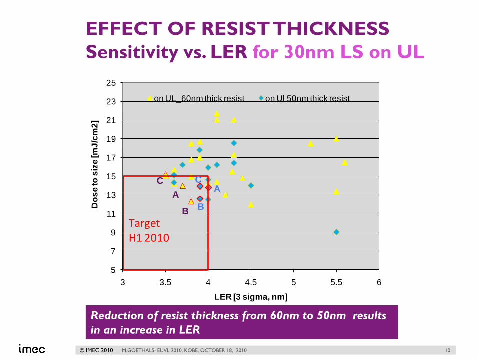
EFFECT OF RESIST THICKNESS
Sensitivity vs. LER for 30nm LS on UL
M.GOETHALS- EUVL 2010, KOBE, OCTOBER 18, 2010 10
Reduction of resist thickness from 60nm to 50nm results
in an increase in LER
5
7
9
11
13
15
17
19
21
23
25
3 3.5 4 4.5 5 5.5 6
Do
se
to
siz
e [m
J/c
m2
]
LER [3 sigma, nm]
on UL_60nm thick resist on Ul 50nm thick resist
TargetH1 2010
B
A
C
B
AC
© IMEC 2010
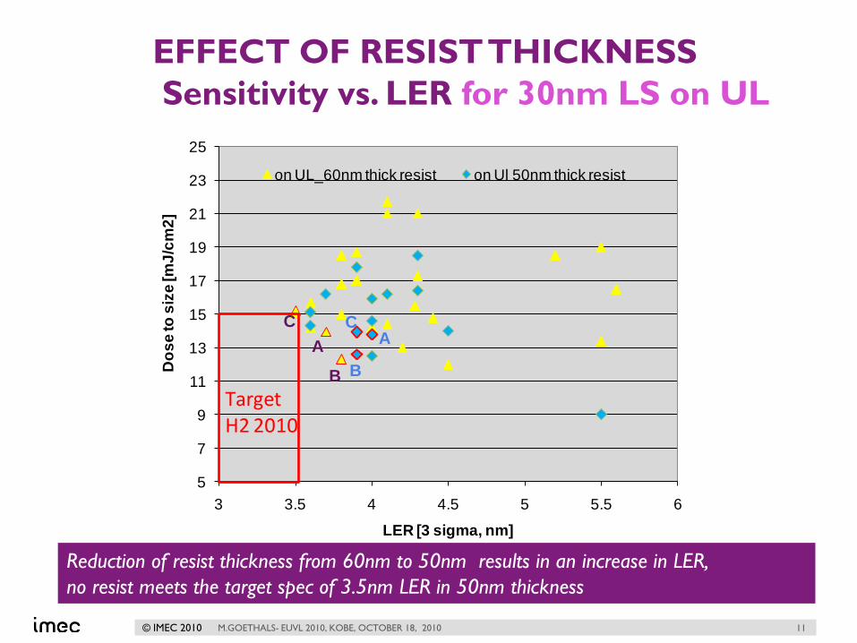
EFFECT OF RESIST THICKNESS
Sensitivity vs. LER for 30nm LS on UL
M.GOETHALS- EUVL 2010, KOBE, OCTOBER 18, 2010 11
Reduction of resist thickness from 60nm to 50nm results in an increase in LER,
no resist meets the target spec of 3.5nm LER in 50nm thickness
5
7
9
11
13
15
17
19
21
23
25
3 3.5 4 4.5 5 5.5 6
Do
se
to
siz
e [m
J/c
m2
]
LER [3 sigma, nm]
on UL_60nm thick resist on Ul 50nm thick resist
TargetH2 2010
B
A
C
B
AC
© IMEC 2010 12
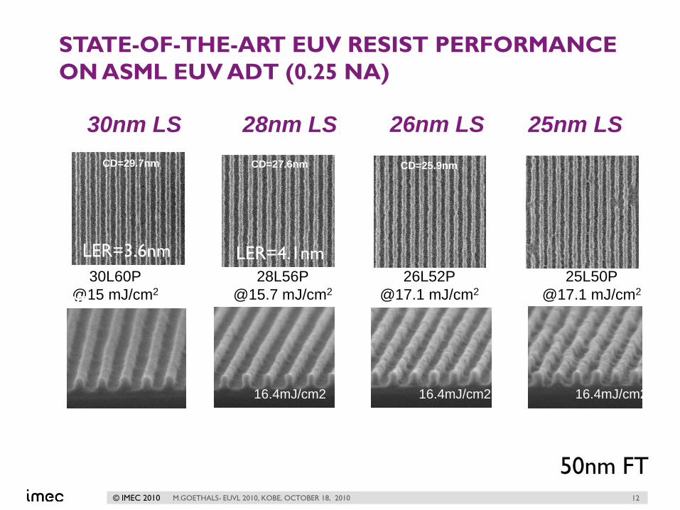
STATE-OF-THE-ART EUV RESIST PERFORMANCE
ON ASML EUV ADT (0.25 NA)
30L60P
@15 mJ/cm2
28L56P
@15.7 mJ/cm2
26L52P
@17.1 mJ/cm2
25L50P
@17.1 mJ/cm2
30nm LS 28nm LS 26nm LS 25nm LS
LER=4.5nm
M.GOETHALS- EUVL 2010, KOBE, OCTOBER 18, 2010
CD=25.9nmCD=27.6nm
16.4mJ/cm2 16.4mJ/cm2 16.4mJ/cm2
CD=30.8nmCD=29.7nm
LER=3.6nm LER=4.1nm
50nm FT
© IMEC 2010
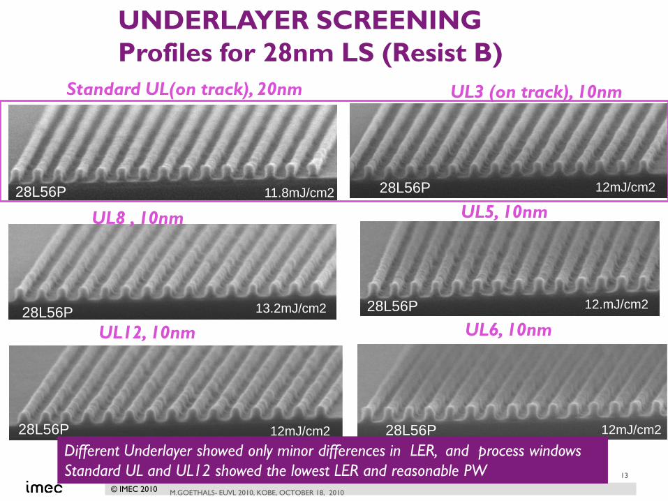
UNDERLAYER SCREENING
Profiles for 28nm LS (Resist B)
M.GOETHALS- EUVL 2010, KOBE, OCTOBER 18, 2010
13
11.8mJ/cm228L56P
13.2mJ/cm228L56P
Standard UL(on track), 20nm
UL8 , 10nm
12mJ/cm228L56P
UL3 (on track), 10nm
12.mJ/cm2
12mJ/cm228L56P
28L56P
UL5, 10nm
UL6, 10nmUL12, 10nm
12mJ/cm228L56P
Different Underlayer showed only minor differences in LER, and process windows
Standard UL and UL12 showed the lowest LER and reasonable PW
© IMEC 2010
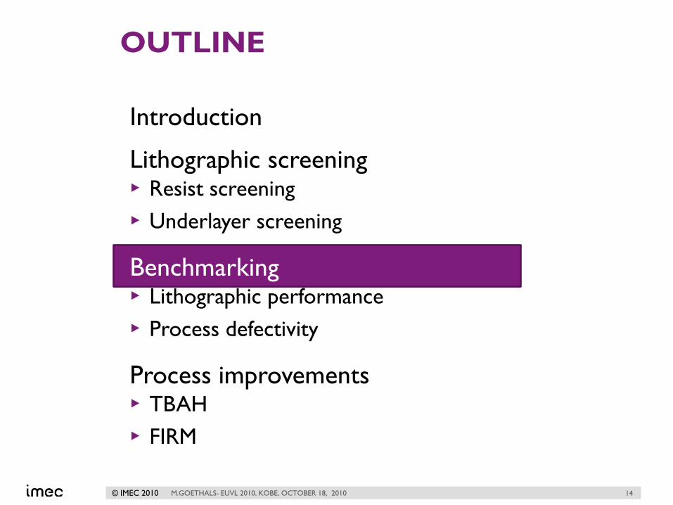
OUTLINE
Introduction
Lithographic screening▸ Resist screening
▸ Underlayer screening
Benchmarking ▸ Lithographic performance
▸ Process defectivity
Process improvements▸ TBAH
▸ FIRM
M.GOETHALS- EUVL 2010, KOBE, OCTOBER 18, 2010 14
© IMEC 2010
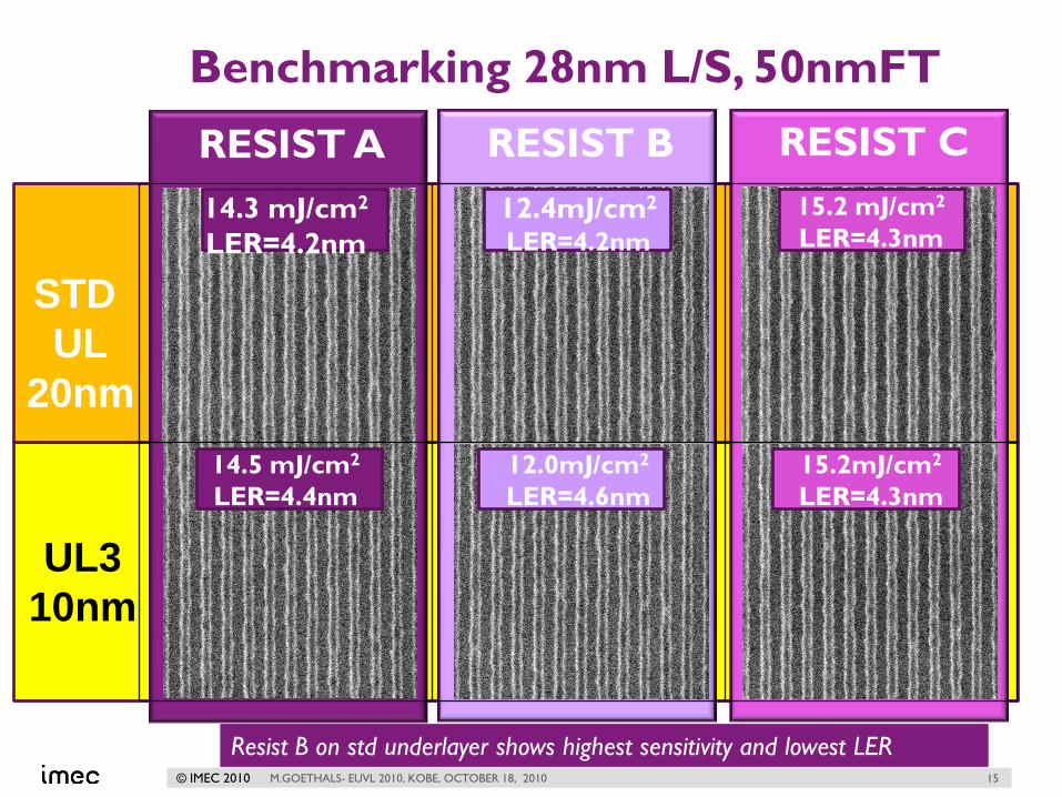
Benchmarking 28nm L/S, 50nmFT
STD
UL
20nm
UL3
10nm
RESIST A RESIST B RESIST C
15M.GOETHALS- EUVL 2010, KOBE, OCTOBER 18, 2010
14.3 mJ/cm2
LER=4.2nm
12.4mJ/cm2
LER=4.2nm
15.2 mJ/cm2
LER=4.3nm
14.5 mJ/cm2
LER=4.4nm
12.0mJ/cm2
LER=4.6nm
15.2mJ/cm2
LER=4.3nm
Resist B on std underlayer shows highest sensitivity and lowest LER
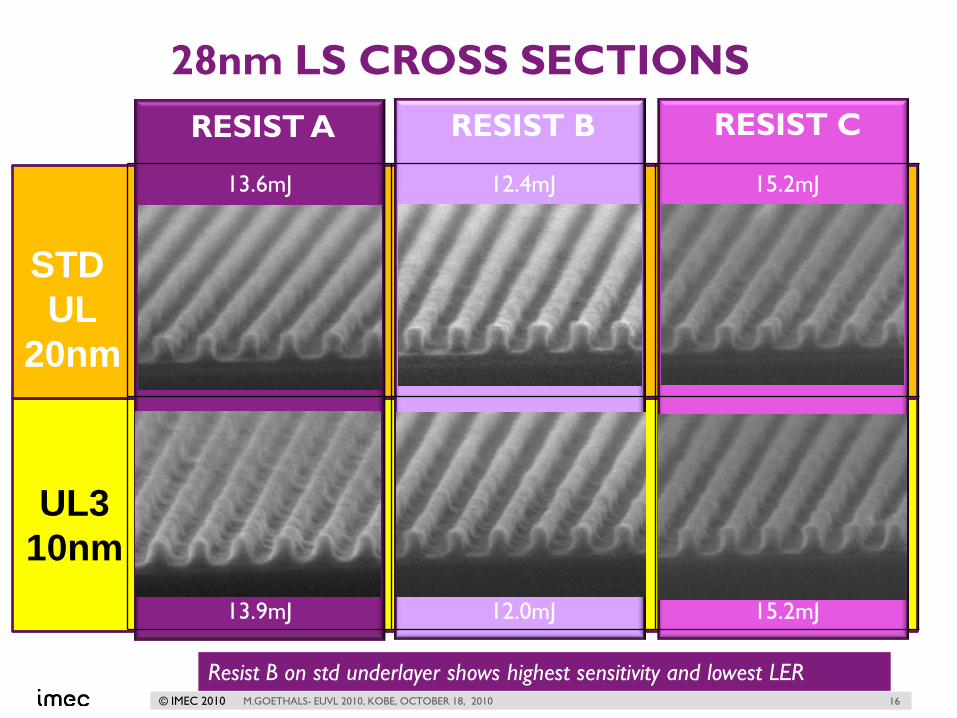
© IMEC 2010
13.6mJ 12.4mJ 15.2mJ
13.9mJ 12.0mJ 15.2mJ
28nm LS CROSS SECTIONS
STD
UL
20nm
UL3
10nm
RESIST A RESIST B RESIST C
16M.GOETHALS- EUVL 2010, KOBE, OCTOBER 18, 2010
Resist B on std underlayer shows highest sensitivity and lowest LER
© IMEC 2010
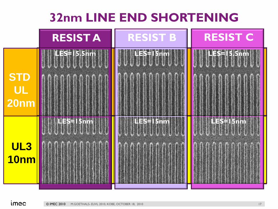
32nm LINE END SHORTENING
STD
UL
20nm
UL3
10nm
RESIST A RESIST B RESIST C
LES=15.5nm LES=15nm LES=15.5nm
LES=15nm LES=15nm LES=15nm
17M.GOETHALS- EUVL 2010, KOBE, OCTOBER 18, 2010
© IMEC 2010
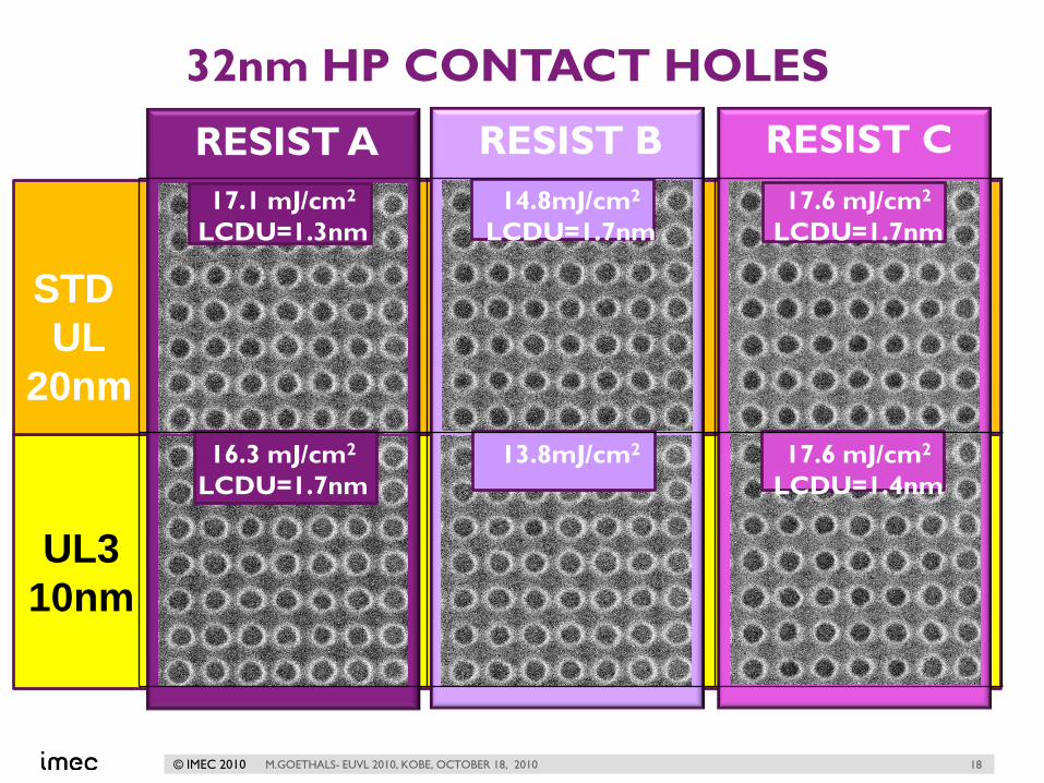
32nm HP CONTACT HOLES
STD
UL
20nm
UL3
10nm
RESIST A RESIST B RESIST C
18M.GOETHALS- EUVL 2010, KOBE, OCTOBER 18, 2010
17.1 mJ/cm2
LCDU=1.3nm
14.8mJ/cm2
LCDU=1.7nm
17.6 mJ/cm2
LCDU=1.7nm
16.3 mJ/cm2
LCDU=1.7nm
13.8mJ/cm2 17.6 mJ/cm2
LCDU=1.4nm
© IMEC 2010
OUTLINE
M.GOETHALS- EUVL 2010, KOBE, OCTOBER 18, 2010 19
Introduction
Lithographic screening▸ Resist screening
▸ Underlayer screening
Benchmarking ▸ Lithographic performance
▸ Process defectivity
Process improvements▸ TBAH
▸ FIRM
© IMEC 2010
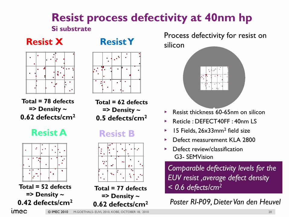
Resist process defectivity at 40nm hpSi substrate
M.GOETHALS- EUVL 2010, KOBE, OCTOBER 18, 2010 20
Process defectivity for resist on
silicon
▸ Resist thickness 60-65nm on silicon
▸ Reticle : DEFECT40FF : 40nm LS
▸ 15 Fields, 26x33mm2 field size
▸ Defect measurement KLA 2800
▸ Defect review/classification
G3- SEMVision
Comparable defectivity levels for the
EUV resist ,average defect density
< 0.6 defects/cm2
Total = 78 defects
=> Density ~
0.62 defects/cm2
Total = 62 defects
=> Density ~
0.5 defects/cm2
Total = 52 defects
=> Density ~
0.42 defects/cm2
Resist X Resist Y
Resist A
Total = 77 defects
=> Density ~
0.62 defects/cm2
Resist B
Poster RI-P09, Dieter Van den Heuvel
© IMEC 2010 21
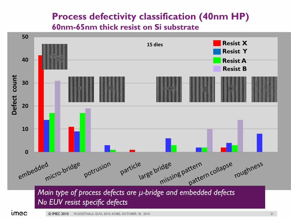
Process defectivity classification (40nm HP)60nm-65nm thick resist on Si substrate
M.GOETHALS- EUVL 2010, KOBE, OCTOBER 18, 2010
0
10
20
30
40
5015 dies
De
fect
co
un
t
Resist X
Resist B
Resist Y
Resist A
Main type of process defects are μ-bridge and embedded defects
No EUV resist specific defects
© IMEC 2010
0
10
20
30
40
50
60
70
15 diesResist B on std UL
Resist C on std UL
De
fect
co
un
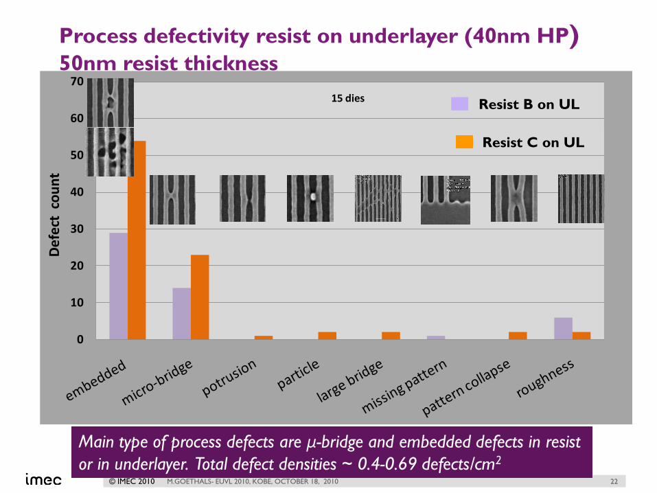
tProcess defectivity resist on underlayer (40nm HP)50nm resist thickness
M.GOETHALS- EUVL 2010, KOBE, OCTOBER 18, 2010 22
Main type of process defects are μ-bridge and embedded defects in resist
or in underlayer. Total defect densities ~ 0.4-0.69 defects/cm2
Resist B on UL
Resist C on UL
© IMEC 2010
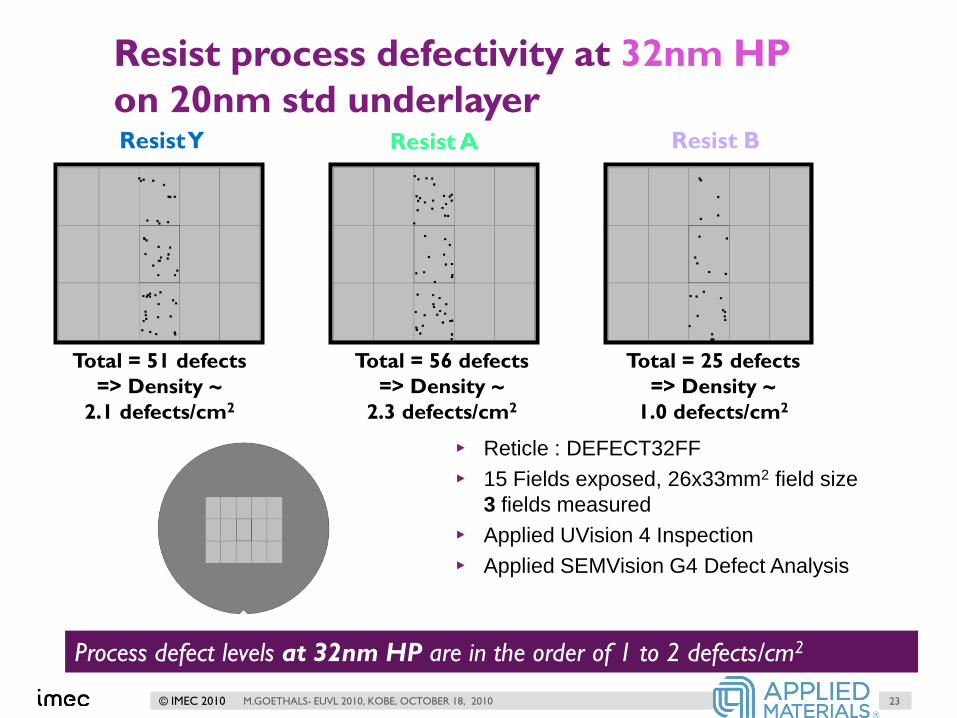
Resist process defectivity at 32nm HP
on 20nm std underlayer
Total = 51 defects
=> Density ~
2.1 defects/cm2
Total = 56 defects
=> Density ~
2.3 defects/cm2
Total = 25 defects
=> Density ~
1.0 defects/cm2
Resist Y Resist A Resist B
▸ Reticle : DEFECT32FF
▸ 15 Fields exposed, 26x33mm2 field size
3 fields measured
▸ Applied UVision 4 Inspection
▸ Applied SEMVision G4 Defect Analysis
Process defect levels at 32nm HP are in the order of 1 to 2 defects/cm2
23M.GOETHALS- EUVL 2010, KOBE, OCTOBER 18, 2010
© IMEC 2010
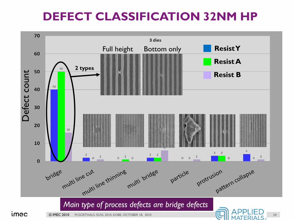
DEFECT CLASSIFICATION 32NM HP
24
Full height Bottom only
2 types
Resist Y
Resist B
Resist A
Main type of process defects are bridge defects
Defe
ct c
ount
M.GOETHALS- EUVL 2010, KOBE, OCTOBER 18, 2010
© IMEC 2010
OUTLINE
Introduction
Lithographic screening▸ Resist screening
▸ Underlayer screening
Benchmarking ▸ Lithographic performance
▸ Process defectivity
Process improvements▸ TBAH
▸ FIRM
M.GOETHALS- EUVL 2010, KOBE, OCTOBER 18, 2010 25
© IMEC 2010
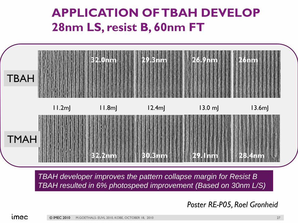
APPLICATION OF TBAH DEVELOP
28nm LS, resist B, 60nm FT
TMAH
11.2mJ 11.8mJ 12.4mJ 13.0 mJ 13.6mJ
TBAH developer improves the pattern collapse margin for Resist B
TBAH resulted in 6% photospeed improvement (Based on 30nm L/S)
32.2nm 30.3nm 29.1nm 28.4nm
TBAH
32.0nm 29.3nm 26.9nm 26nm
Poster RE-P05, Roel Gronheid
27M.GOETHALS- EUVL 2010, KOBE, OCTOBER 18, 2010
© IMEC 2010
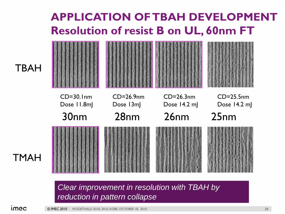
APPLICATION OF TBAH DEVELOPMENT
Resolution of resist B on UL, 60nm FT
30nm 28nm 26nm 25nm
CD=26.3nm
Dose 14.2 mJ
CD=25.5nm
Dose 14.2 mJ
CD=26.9nm
Dose 13mJ
CD=30.1nm
Dose 11.8mJ
TBAH
TMAH
Clear improvement in resolution with TBAH by
reduction in pattern collapse
28M.GOETHALS- EUVL 2010, KOBE, OCTOBER 18, 2010
© IMEC 2010
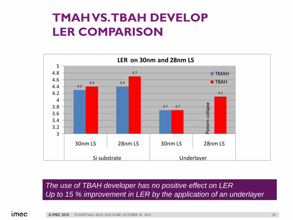
TMAH VS. TBAH DEVELOP
LER COMPARISON
The use of TBAH developer has no positive effect on LER
Up to 15 % improvement in LER by the application of an underlayer
29M.GOETHALS- EUVL 2010, KOBE, OCTOBER 18, 2010
4.34.4
3.7
4.4
4.7
3.7
4.1
33.23.43.63.8
44.24.44.64.8
5
30nm LS 28nm LS 30nm LS 28nm LS
Si substrate Underlayer
LER on 30nm and 28nm LS
TMAH
TBAH
© IMEC 2010
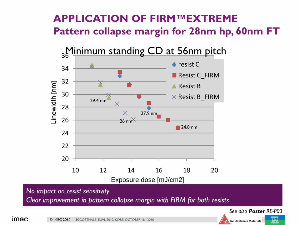
APPLICATION OF FIRM™EXTREME
Pattern collapse margin for 28nm hp, 60nm FT
30
20
22
24
26
28
30
32
34
36
10 12 14 16 18 20
resist C
Resist C_FIRM
Resist B
Resist B_FIRM29.4 nm
26 nm
24.8 nm
27.9 nm
Exposure dose [mJ/cm2]
No impact on resist sensitivity
Clear improvement in pattern collapse margin with FIRM for both resists
M.GOETHALS- EUVL 2010, KOBE, OCTOBER 18, 2010
See also Poster RE-P03
Minimum standing CD at 56nm pitch
© IMEC 2010
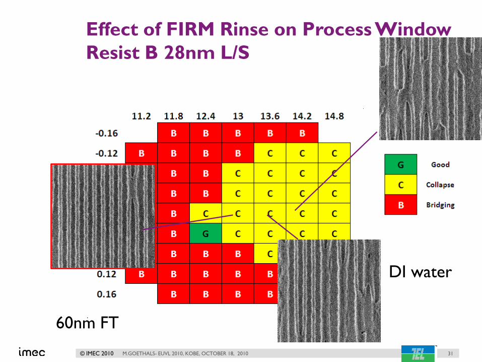
Effect of FIRM Rinse on Process Window
Resist B 28nm L/S
M.GOETHALS- EUVL 2010, KOBE, OCTOBER 18, 2010 31
DI water
60nm FT
© IMEC 2010
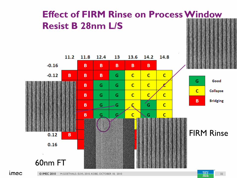
Effect of FIRM Rinse on Process Window
Resist B 28nm L/S
M.GOETHALS- EUVL 2010, KOBE, OCTOBER 18, 2010 32
PORFIRM Rinse
60nm FT
© IMEC 2010
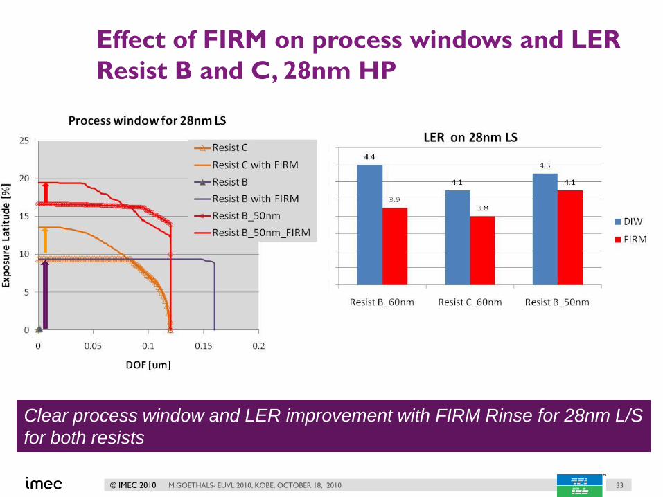
Effect of FIRM on process windows and LER
Resist B and C, 28nm HP
M.GOETHALS- EUVL 2010, KOBE, OCTOBER 18, 2010 33
Clear process window and LER improvement with FIRM Rinse for 28nm L/S
for both resists
© IMEC 2010
ResolutionResist B
DI-water
Resist B
FIRM
Resist C
Di-water
Resist C
FIRM
28nm HP
26nm HP
25nm HP
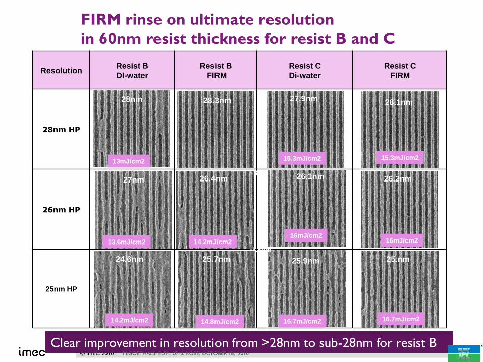
FIRM rinse on ultimate resolution
in 60nm resist thickness for resist B and C
34
Clear improvement in resolution from >28nm to sub-28nm for resist B
26.1nm
25.9nm
24.8nm
24.5nm
15.3mJ/cm2
16mJ/cm2
16.7mJ/cm2
13mJ/cm2
27.9nm
15.3mJ/cm2
28.1nm
26.2nm
16mJ/cm2
16.7mJ/cm2
25.nm
28nm
13mJ/cm2
13.6mJ/cm2
27nm
14.2mJ/cm2
24.6nm
28.3nm
14.2mJ/cm2
26.4nm
14.8mJ/cm2
25.7nm
M.GOETHALS- EUVL 2010, KOBE, OCTOBER 18, 2010
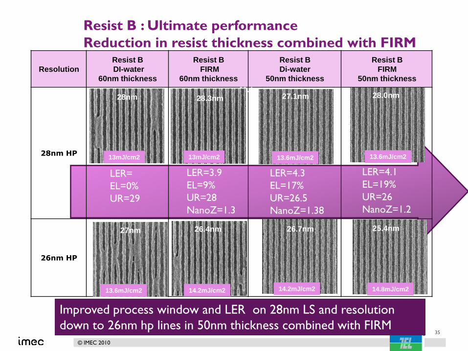
© IMEC 2010
Resolution
Resist B
DI-water
60nm thickness
Resist B
FIRM
60nm thickness
Resist B
Di-water
50nm thickness
Resist B
FIRM
50nm thickness
28nm HP
26nm HP
Resist B : Ultimate performance
Reduction in resist thickness combined with FIRM
35
28.4nm
15.3mJ/cm213mJ/cm2
27.9nm28nm
13mJ/cm2
28.3nm 27.1nm
13.6mJ/cm2 13.6mJ/cm2
28.0nm
M.GOETHALS- EUVL 2010, KOBE, OCTOBER 18, 2010
LER=3.9
EL=9%
UR=28
NanoZ=1.3
LER=
EL=0%
UR=29
13mJ/cm2
LER=4.3
EL=17%
UR=26.5
NanoZ=1.38
LER=4.1
EL=19%
UR=26
NanoZ=1.2
13.6mJ/cm2
27nm
14.2mJ/cm2
26.4nm 26.7nm
14.2mJ/cm2
25.4nm
14.8mJ/cm2
Improved process window and LER on 28nm LS and resolution
down to 26nm hp lines in 50nm thickness combined with FIRM
© IMEC 2010
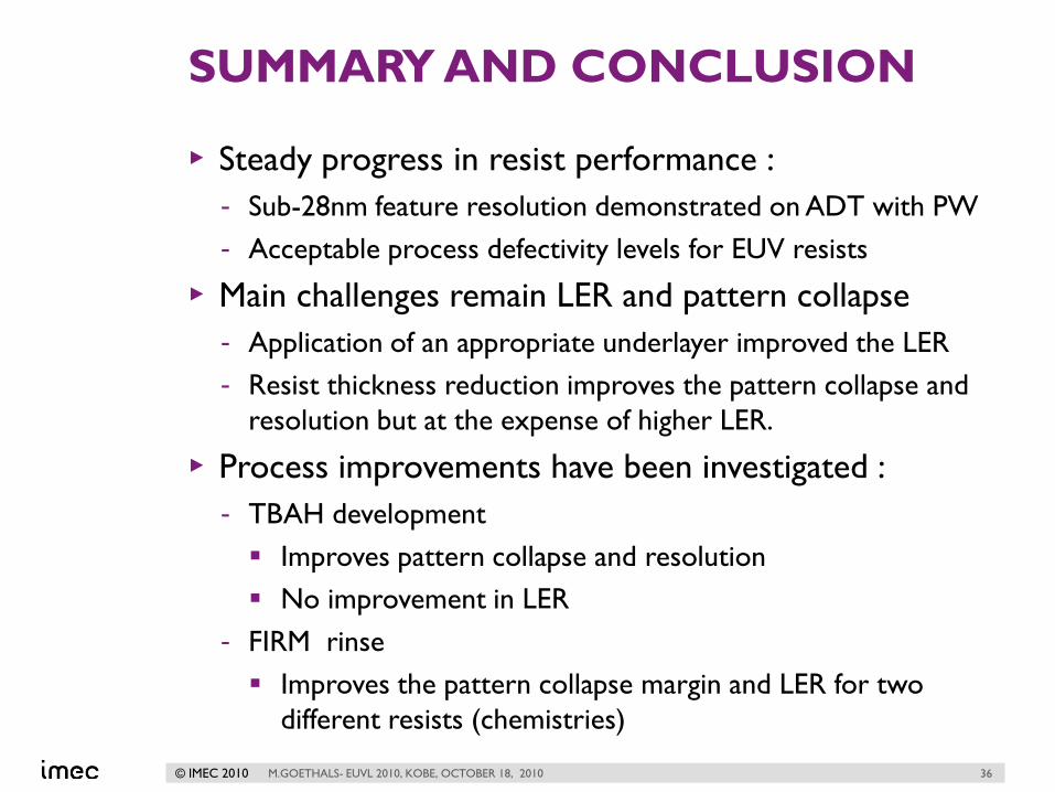
SUMMARY AND CONCLUSION
▸ Steady progress in resist performance :
- Sub-28nm feature resolution demonstrated on ADT with PW
- Acceptable process defectivity levels for EUV resists
▸ Main challenges remain LER and pattern collapse
- Application of an appropriate underlayer improved the LER
- Resist thickness reduction improves the pattern collapse and
resolution but at the expense of higher LER.
▸ Process improvements have been investigated :
- TBAH development
Improves pattern collapse and resolution
No improvement in LER
- FIRM rinse
Improves the pattern collapse margin and LER for two
different resists (chemistries)
M.GOETHALS- EUVL 2010, KOBE, OCTOBER 18, 2010 36
© IMEC 2010
ACKNOWLEDGMENTS
ASML▸ ADT team at IMEC
TEL ▸ Neil Bradon, Kathleen Nafus, Shane 0’Neill, Hideo Shite
IMEC▸ Roel Gronheid, Geert Vandenberghe, Eric Hendrickx, Jan
Hermans
Material suppliers ▸ For supplying the samples and useful discussions
AMAT▸ Moshe Rozentsvige, Kfir Dotan, Chris S. Ngai
Part of this work was sponsored by CATRENE through the project CT301 EXEPT
M.GOETHALS- EUVL 2010, KOBE, OCTOBER 18, 2010 37