Evaluation and optimization of NIR HgCdTe Avalanche Photodiode Arrays for Adaptive Optics and Interferometry Gert Finger a , Ian Baker b , Domingo Alvarez a , Derek Ives a , Leander Mehrgan a , Manfred Meyer a , Jörg Stegmeier a , Peter Thorne b and Harald J. Weller b . a European Southern Observatory, Karl Schwarzschildstrasse 2, D-85748-Garching, Germany. b SELEX Galileo Infrared Ltd, Southampton, Hants, SO15 OLG, UK. ABSTRACT The performance of the current high speed near infrared HgCdTe sensors operating in fringe trackers, wavefront sensors and tip-tilt sensors is severely limited by the noise of the silicon readout interface circuit (ROIC), even if state-of-the- art CMOS designs are used. A major improvement can only be achieved by the amplification of the photoelectron signal directly at the point of absorption by means of avalanche gain inside the infrared pixel. Unlike silicon, HgCdTe offers noiseless avalanche gain. This has been verified with the LPE grown 320x256 pixel c =2.5 m HgCdTe eAPD arrays from SELEX both on a prototype ROIC called SWALLOW and on a newly developed ROIC, specifically designed for AO applications, called SAPHIRA. The novel features of the new SAPHIRA ROIC, which has 32 parallel video chan- nels operating at 5 MHz, will be described, together with the new high speed NGC data acquisition system. Performance results will be discussed for both ROICs. The LPE material on the SWALLOW prototype was excellent and allowed operation at an APD gain as high as 33. Unfortunately, the LPE material of the first devices on the SAPHIRA ROIC suf- fers from problems which are now understood. However, due to the excellent performance of the SAPHIRA ROIC even with the limitations of present HgCdTe material, it is possible with simple double correlated sampling to detect test pat- terns with signal levels of 1 electron. An outlook will be given on further developments of heterojunctions grown by MOVPE, which eventually may replace eAPD arrays grown by LPE. Keywords: Keywords: avalanche photodiode, eAPD, HgCdTe, readout noise, excess noise. APD gain, cryogenic am- plifier, infrared, wavefront sensor, fringe tracker 1. INTRODUCTION Fringe tracking and infrared wavefront sensing are restricted to bright sources mainly because of the high readout speed (frame rate ~1kHz) required to cope with the changes of the wavefront distortions caused by the turbulent atmosphere. This entails opening up the analog bandwidth and limits the sensitivity of current CMOS readouts to values between 60 and 100 e- rms. The avalanche gain mechanism has already successfully been used as a noiseless gain mechanism inside infrared pixels to enhance the sensitivity in laser gated imaging. Hence, it seemed a logical next step to investigate whether this gain mechanism could also be employed for infrared wavefront sensing and fringe tracking. Since the inte- gration times for wavefront sensing are in the millisecond regime and the integration times for laser gated imaging are typically in the nanosecond range, then the cutoff wavelength of HgCdTe had to be changed from 4.2 microns to 2.5 microns to reduce the dark current to an acceptable level. The change of cutoff wavelength reduces both the dark current and the APD gain. The British company SELEX-Galileo Infrared Ltd had already accumulated considerable experience with eAPD arrays in laser gated three dimensional (3D) imaging. Therefore, three years ago ESO initiated at SELEX the development of HgCdTe eAPD arrays having cutoff wavelengths of c ~2.5 m. 2. HGCDTE EAPD TECHNOLOGY The solid state mechanisms for avalanche gain in HgCdTe have been well described and two recommended papers are [1] and [2], together with the reference lists. Figure 1 shows a potential energy schematic for a typical photodiode which
Transcript
Evaluation and optimization of NIR HgCdTe Avalanche Photodiode Arrays for Adaptive Optics and Interferometry
Gert Fingera, Ian Bakerb, Domingo Alvarez a, Derek Ivesa, Leander Mehrgana, Manfred Meyera, Jörg
Stegmeiera , Peter Thorneb and Harald J. Wellerb. aEuropean Southern Observatory, Karl Schwarzschildstrasse 2, D-85748-Garching, Germany.
b SELEX Galileo Infrared Ltd, Southampton, Hants, SO15 OLG, UK.
ABSTRACT
The performance of the current high speed near infrared HgCdTe sensors operating in fringe trackers, wavefront sensors and tip-tilt sensors is severely limited by the noise of the silicon readout interface circuit (ROIC), even if state-of-the- art CMOS designs are used. A major improvement can only be achieved by the amplification of the photoelectron signal directly at the point of absorption by means of avalanche gain inside the infrared pixel. Unlike silicon, HgCdTe offers noiseless avalanche gain. This has been verified with the LPE grown 320x256 pixel c=2.5m HgCdTe eAPD arrays from SELEX both on a prototype ROIC called SWALLOW and on a newly developed ROIC, specifically designed for AO applications, called SAPHIRA. The novel features of the new SAPHIRA ROIC, which has 32 parallel video chan-nels operating at 5 MHz, will be described, together with the new high speed NGC data acquisition system. Performance results will be discussed for both ROICs. The LPE material on the SWALLOW prototype was excellent and allowed operation at an APD gain as high as 33. Unfortunately, the LPE material of the first devices on the SAPHIRA ROIC suf-fers from problems which are now understood. However, due to the excellent performance of the SAPHIRA ROIC even with the limitations of present HgCdTe material, it is possible with simple double correlated sampling to detect test pat-terns with signal levels of 1 electron. An outlook will be given on further developments of heterojunctions grown by MOVPE, which eventually may replace eAPD arrays grown by LPE.
Fringe tracking and infrared wavefront sensing are restricted to bright sources mainly because of the high readout speed (frame rate ~1kHz) required to cope with the changes of the wavefront distortions caused by the turbulent atmosphere. This entails opening up the analog bandwidth and limits the sensitivity of current CMOS readouts to values between 60 and 100 e- rms. The avalanche gain mechanism has already successfully been used as a noiseless gain mechanism inside infrared pixels to enhance the sensitivity in laser gated imaging. Hence, it seemed a logical next step to investigate whether this gain mechanism could also be employed for infrared wavefront sensing and fringe tracking. Since the inte-gration times for wavefront sensing are in the millisecond regime and the integration times for laser gated imaging are typically in the nanosecond range, then the cutoff wavelength of HgCdTe had to be changed from 4.2 microns to 2.5 microns to reduce the dark current to an acceptable level. The change of cutoff wavelength reduces both the dark current and the APD gain. The British company SELEX-Galileo Infrared Ltd had already accumulated considerable experience with eAPD arrays in laser gated three dimensional (3D) imaging. Therefore, three years ago ESO initiated at SELEX the development of HgCdTe eAPD arrays having cutoff wavelengths of c ~2.5 m.
2. HGCDTE EAPD TECHNOLOGY
The solid state mechanisms for avalanche gain in HgCdTe have been well described and two recommended papers are [1] and [2], together with the reference lists. Figure 1 shows a potential energy schematic for a typical photodiode which
illustrates the single-carrier, cascade-like gain mechanism, together with the history-dependent behaviour that leads to the observed low excess noise factors. In HgCdTe this is an electron gain mechanism so the absorber must be P-type, which favours an N-on-P structure. Theoretical studies indicate that there is an optimum width for the depletion region (gain zone) of 1.5 to 2.5µm, at the lower end of this range there is a risk of gain saturation and tunneling currents; while at the upper end, alloy or phonon scattering starts to impact the ionisation threshold voltage. One of the reasons APD arrays have matured so quickly is that these conditions are easily met using near-standard manufacturing processes.
Figure 1 Band diagram illustrating history-dependent avalanche gain in HgCdTe. For NIR wavefront sensing the HgCdTe eAPD can give more than an order of magnitude improvement in signal-to-noise ratio. The well known advantages are: voltage controlled signal gain at the point of absorption, an excess noise factor close to unity, negligible non-uniformity and near zero power consumption. On the cautionary side, the excess noise fac-tor of HgCdTe eAPDs is often quoted as being close to unity but APD noise figures only describe the gain fluctuation. Noise due to dark current is not included and can be significant, particularly as it is gain-amplified in many devices. Prior to the astronomical applications the development of APDs was concentrated on 4.5 µm cutoff material, high gain and short integration times for burst illumination LIDAR type-applications. The astronomy devices essentially use the same process but with the LPE material grown at a shorter wavelength (2.5 µm). The longer integration times have elevated the importance of dark current and noisy pixels associated with excessive dark current for which there is not a strong database at 2.5 µm. The best arrays achieve a gain value of x33 at a bias of 12.4V for integration times of 5ms, although deep cooling is usually needed to suppress defective pixels. More investment will be needed by the astronomy communi-ty to extract the maximum signal-to-noise benefit from HgCdTe eAPDs. There are two HgCdTe technologies available for APD detectors at SELEX, including the 2nd generation LPE/via-hole process [3][4] and 3rd generation processes based on MOVPE (metalorganic vapor phase epitaxy), bump-bonded hybrids [5][6]. Figure 2 shows a schematic description of the technologies. Up to the present time, all short wavelength APD arrays have used the LPE/via-hole process and this has given very consistent exponential avalanche gain and outstanding reverse-bias breakdown voltage. It has the advantage of very beneficial junction geometry for avalanche gain and since the photons are absorbed at the top surface, it is sensitive over a wide spectral range. Dark currents are higher than MOVPE but for wavefront sensors and most interferometric applications, the dark current specification of <1e-9 A.cm2 is easily met. On the negative side for low flux/high gain applications the junction position and the fixed charge in the passivation needs to be more tightly controlled than with conventional focal plane arrays and this has led to some incon-sistency in the defect levels of APD arrays from batch to batch. Nevertheless the LPE/via-hole process provides the best science grade arrays at present.
Heavy hole mass – 0.55m0 - rapid energy loss due to phonon scatteringHole mobility << electron mobility
hv
Potential energy
P-type absorber
N-type region
Low doped avalanche region
Electron impact ionisation
Heavy hole mass – 0.55m0 - rapid energy loss due to phonon scatteringHole mobility << electron mobility
hv
Potential energy
P-type absorber
N-type region
Low doped avalanche region
Electron impact ionisation
Figure 2 Schematics of device structures used for APDs
3. PERFORMANCE WITH SWALLOW PROTOTYPE AND LPE/VIA-HOLE TECHNOLOGY
In a previous paper [7] it was demonstrated that an eAPD array hybridized to an existing SWALLOW ROIC can achieve classic avalanche gain up to x20 at a 9V bias, a readout noise of < 7 e- rms and a dark current compliant with the re-quirements of AO wavefront sensing [7]. The ROIC was modified to reduce the multiplexer glow by adding additional metal screens. Furthermore, a protection circuit had to be removed to allow high reverse bias voltages. LPE material of exceptionally high quality was grown and hybridized to the modified ME8 ROIC which allowed the application of bias voltages up to 13 V. The measured APD gain versus applied bias voltage is represented by black squares in Figure 3, the solid red curve is an exponential fit. At a bias voltage of 12.7 V the APD gain is 33.
Figure 3 APD gain as function of bias voltage.
Avalanche region n-
Graded composition
P+ to p-
N+
hvP absorber
Avalanche region n-
N+
hv
LPE/via-hole technology
MOVPE/mesa technology
Avalanche region n-
Graded composition
P+ to p-
N+
hvP absorber
Avalanche region n-
N+
hv
LPE/via-hole technology
MOVPE/mesa technology
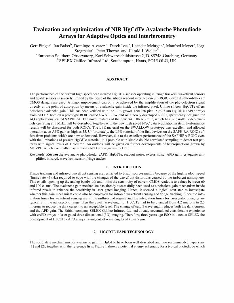
The integrating node of the unit cell in the SWALLOW multiplexer is directly accessible (see Figure 2 in [7]). Keeping the array common, at the anode side of the HgCdTe junction, at a fixed voltage and changing the voltage PRV on the cathode side of the junction, yields the number of digital ADU’s per Volt. The same calibration can be made by keeping the video output of the detector fixed and varying the external offset voltage of the symmetric preamplifier shown on the right side of Figure 13. The ratio of the voltage change at the integrating node and the detector output is the transfer function which was measured to be 0.58 for the SWALLOW ROIC. The conversion gain is derived from the photon transfer curve by measuring the variance versus the signal at different flux levels. The integration time was set to 6.9 ms and the flux was varied by changing the blackbody temperature. From the inverse slope of data in Figure 4 a gain of 12.8 electrons/ADU was retrieved which corresponds to a nodal capacitance of 69fF or a conversion gain of 2.30 V/electron. This agrees well with the values expected from design. The conversion gain as determined from Figure 4 was measured at different bias voltages corresponding to different APD gains. The noise figure or excess noise factor of APD’s is defined as the noise associated with the gain process. The result of this excess noise factor is that the noise increases with gain faster than the signal. Hence the signal to noise ratio of the detector is actually degraded by the APD gain if the excess noise factor is larger than 1. The excess noise factor can be determined by plotting the conversion gain normalized at unity APD gain as a function of reverse bias voltage and dividing by the APD signal gain. Since the conversion gain is proportional to the variance, the square root of the ob-tained curve is the excess noise factor. It is plotted in Figure 5 as a function of APD gain. The excess noise factor is less than 1.1 up to an APD gain of 33, a very encouraging result. As shown in Figure 6 the almost noiseless amplification of the avalanche process is a new and powerful tool to further boost the sensitivity of infrared detectors and overcome the readout noise floor of state of the art CMOS multiplexers. Two noise histograms are shown for correlated double sam-pling (CDS). The noise histogram for CDS at unity APD gain peaks at 124 e-rms. With an APD gain of 33 the readout noise is reduced to 3.2 e- rms, at a pixel rate of 5 MHz/channel. Further noise reduction is demonstrated with Fowler sampling, taking 8 Fowler pairs in combination with 4 sub-pixel samples. Sub-pixel sampling is described in chapter 0. The noise histogram for the 8 Fowler pairs in Figure 6 peaks at 1 e-rms. It was measured by taking the average of 4 ADC conversions per pixel.
Figure 4 Photon transfer curve of SWALLOW ME788 ROIC at unity APD gain and a reverse bias voltage of 0.91V.
Figure 6 Noise histogram of SWALLOW ME788 prototype eAPD array at operating temperature of T=40K. Noise: at unity APD gain with CDS 124 e-rms, at APD gain of 33 with CDS: 3.2 e-rms and with 8 Fowler pairs and 4 sub-pixel samples 1 e-rms
In Figure 7 the median of the Fowler readout noise is plotted versus the number of non-destructive readouts, for different operating temperatures. The APD gain was 33. The readout time of a single 320x256 pixel non-destructive frame is 5 ms for the SWALLOW ROIC, which only has 4 outputs. The number of non-destructive readouts on the horizontal axis of Figure 7 times 5 ms is the integration time for continuous non-destructive readouts. The temperature dependence for a large number of readouts is weak. The readout noise of 3 e-rms for CDS is reduced to <1.3 e-rms for 8 Fowler pairs. The minimum integration time for 8 Fowler pairs is 80 ms. At larger numbers of non-destructive readouts and longer integra-tion times the readout noise starts to rise because of the dark current and its associated shot noise.
Figure 7 Readout noise with Fowler sampling versus number of non-destructive readouts for APD gain of 33.
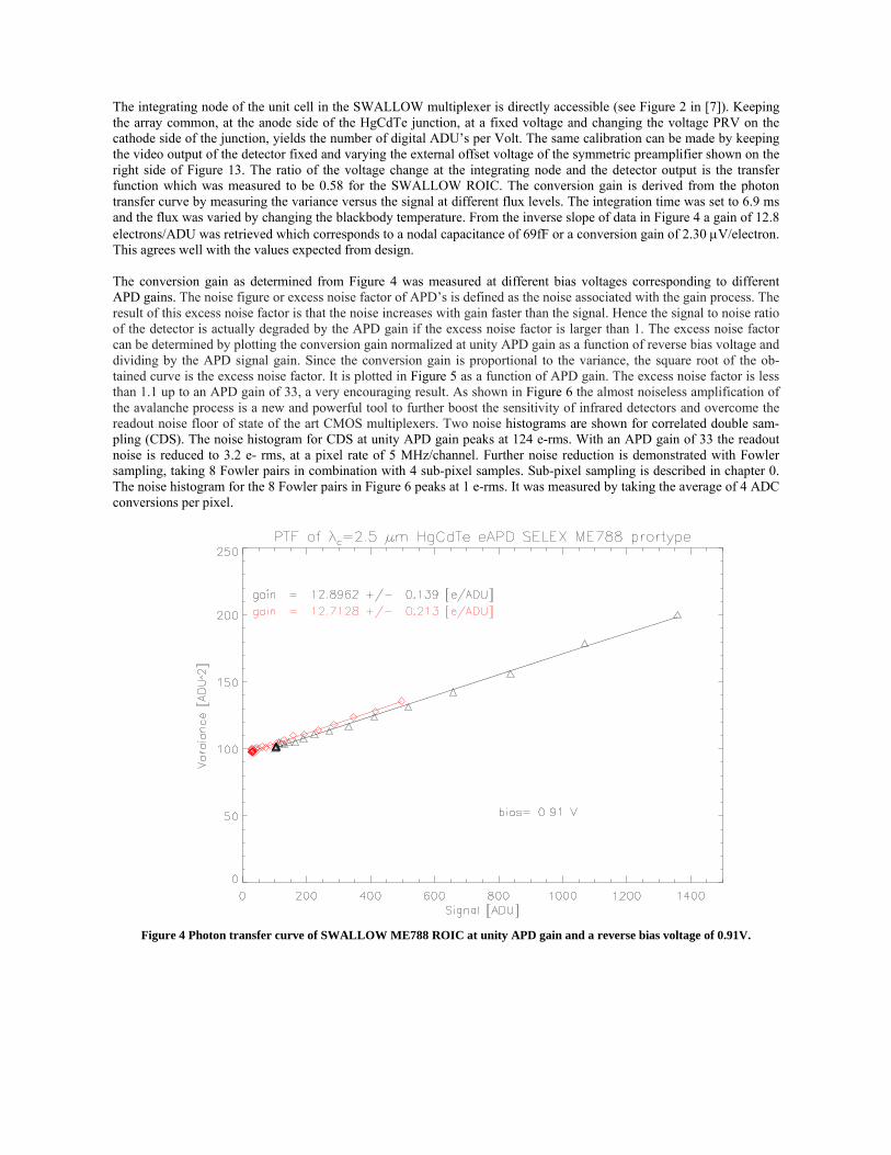
Figure 8 shows the cosmetic quality of flat-fielded images taken for the highest APD gain of 33 while operating the de-tector at temperatures of 30K (left image) and at 80K (right image). The flat-fields are the ratio of two difference images. One difference image was obtained by illuminating the detector with a blackbody at temperatures of 60C and 20C and the other difference image at temperatures of 50C and 20C. The cut levels of the image are 0 and 1. In Figure 9 the fraction of bad pixels is plotted as a function of temperature for different bias voltages. The uppermost curve taken at a bias of 12.8V corresponds to an APD gain of 33. The need for operating the detector below the tempera-ture of liquid nitrogen at high APD gain is evident. To meet this need a small low vibration Stirling-type pulse tube coo-ler running at 50Hz is being developed which has its warm end at T=80K and will provide a cooling power of 2W at a temperature of T=40K. It will be used in the wavefront sensors of the second generation VLTI instrument GRAVITY [10]. The detectors are operating in a liquid nitrogen cryostat and the pulse tube will only be used to cool the detector to temperatures below 77K. The quantum efficiency is a function of temperature as shown in Figure 10. It rises from 28.4% to 51.8% in H-band and from 37.6% to 66.6% in K-band when the detector is cooled from T=80K to T=40K. Apart from the improved cosmetics the gain in quantum efficiency is the second reason why it is desirable to operate the APD array at temperatures of 40K.
To demonstrate the sensitivity of the SWALLOW prototype sensor, a test pattern consisting of a grid of holes was illu-minated by an extended blackbody and imaged onto the detector. Taking differences of images observed at two blackbo-dy temperatures generates a pattern having a calibrated flux which is 1.75 electrons. It can be detected as shown in Fig-ure 11. The image is an average of 16 DCS frames taken with an integration time of 5 ms.
Figure 8 Comparison of the cosmetic quality of flat-fielded images at an APD gain of 33
Figure 9 Cosmetic quality versus temperature. Bad pixel of flat-field defined as deviating 30 % from median.
Figure 10 Quantum efficiency as function of temperature in H and K band.
Figure 11 Calibrated flux in circular holes corresponding to a signal difference of 1.7 electrons. The image is an average of 16
DCS frames taken with an integration time of 5 ms and an APD gain of 33
4. CUSTOM SPECIFIC SAPHIRA ROIC
The results obtained with c=2.5m NIR eAPD arrays have been very encouraging. However, it also became evident that the SWALLOW ROIC, which was developed for laser gated imaging was not ideally matched to the requirements of adaptive optics and interferometry. Therefore, ESO decided to fund a new custom specific ROIC design, tailored to the special needs of the wavefront sensing and fringe tracking needed for the second generation VLTI instrument GRAVI-TY. The main goal was to achieve better sensitivity by optimizing the CMOS design to target the lowest possible noise floor. Starting with a lower readout noise, the same sensitivity can be achieved with a lower APD gain an thus better cosmetic quality, a key issue of APD arrays at higher gain.
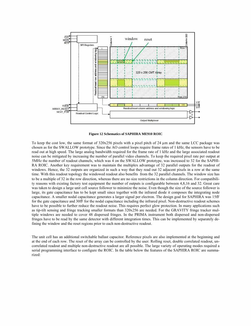
Figure 12 Schematics of SAPHIRA ME910 ROIC To keep the cost low, the same format of 320x256 pixels with a pixel pitch of 24 m and the same LCC package was chosen as for the SWALLOW prototype. Since the AO control loops require frame rates of 1 kHz, the sensors have to be read out at high speed. The large analog bandwidth required for the frame rate of 1 kHz and the large associated readout noise can be mitigated by increasing the number of parallel video channels. To keep the required pixel rate per output at 5MHz the number of readout channels, which was 4 on the SWALLOW prototype, was increased to 32 for the SAPHI-RA ROIC. Another key requirement was to maintain the multiplex advantage of 32 parallel outputs for the readout of windows. Hence, the 32 outputs are organized in such a way that they read out 32 adjacent pixels in a row at the same time. With this readout topology the windowed readout also benefits from the 32 parallel channels. The window size has to be a multiple of 32 in the row direction, whereas there are no size restrictions in the column direction. For compatibili-ty reasons with existing factory test equipment the number of outputs is configurable between 4,8,16 and 32. Great care was taken to design a large unit cell source follower to minimize the noise. Even though the size of the source follower is large, its gate capacitance has to be kept small since together with the infrared diode it composes the integrating node capacitance. A smaller nodal capacitance generates a larger signal per electron. The design goal for SAPHIRA was 15fF for the gate capacitance and 30fF for the nodal capacitance including the infrared pixel. Non-destructive readout schemes have to be possible to further reduce the readout noise. This requires perfect glow protection. In many applications such as tip-tilt sensing and fringe tracking smaller formats than 320x256 are needed. For the GRAVITY fringe tracker mul-tiple windows are needed to cover 48 dispersed fringes. In the PRIMA instrument both dispersed and non-dispersed fringes have to be read by the same detector with different integration times. This can be implemented by separately de-fining the window and the reset regions prior to each non-destructive readout. The unit cell has an additional switchable ballast capacitor. Reference pixels are also implemented at the beginning and at the end of each row. The reset of the array can be controlled by the user. Rolling reset, double correlated readout, un-correlated readout and multiple non-destructive readout are all possible. The large variety of operating modes required a serial programming interface to configure the ROIC. In the table below the features of the SAPHIRA ROIC are summa-rized:
Key features of SPAHIRA ROIC:
o format: 320 x 256 NIR HgCdTe Diode Array o full frame readout in less than 500s with 5MHz clock o lowest possible readout noise with special care to SFD design o high conversion gain : low capacitance of integrating node o multiple sub-frame windowing readout modes with multiplex advantage o nondestructive readout, Rolling-Reset (RR) and Read-Reset-Read (RrR) imaging modes o selectable reference pixels o SPI control interface o selectable internal or external array reset pulse o user programmable pixel voltage clamp o Internal slew rate and time constant control
In Figure 12 the shift register based addressing of the SAPHIRA windowing scheme is shown. For the row addresses, a bit stream of 256 bits have to be loaded and for the column addresses, 10 bits (320 pixel= 10x32 pixel) have to be loaded to address the required readout window. The reset regions have to be addressed in the same way. If a 5 MHz clock is used, then the download of the readout and reset windows takes 106.4 s. This overhead can be reduced with faster clocking. The separate window addressing capability for readout (green regions in Figure 12) and reset windows (yellow regions in Figure 12) makes it possible to have different integration times for different windows when the multiple non-destructive readout scheme is used. Furthermore, possible edge effects can be avoided when the reset region is made larger than the readout region.
5. CRYOGENIC PREAMPLIFIERS
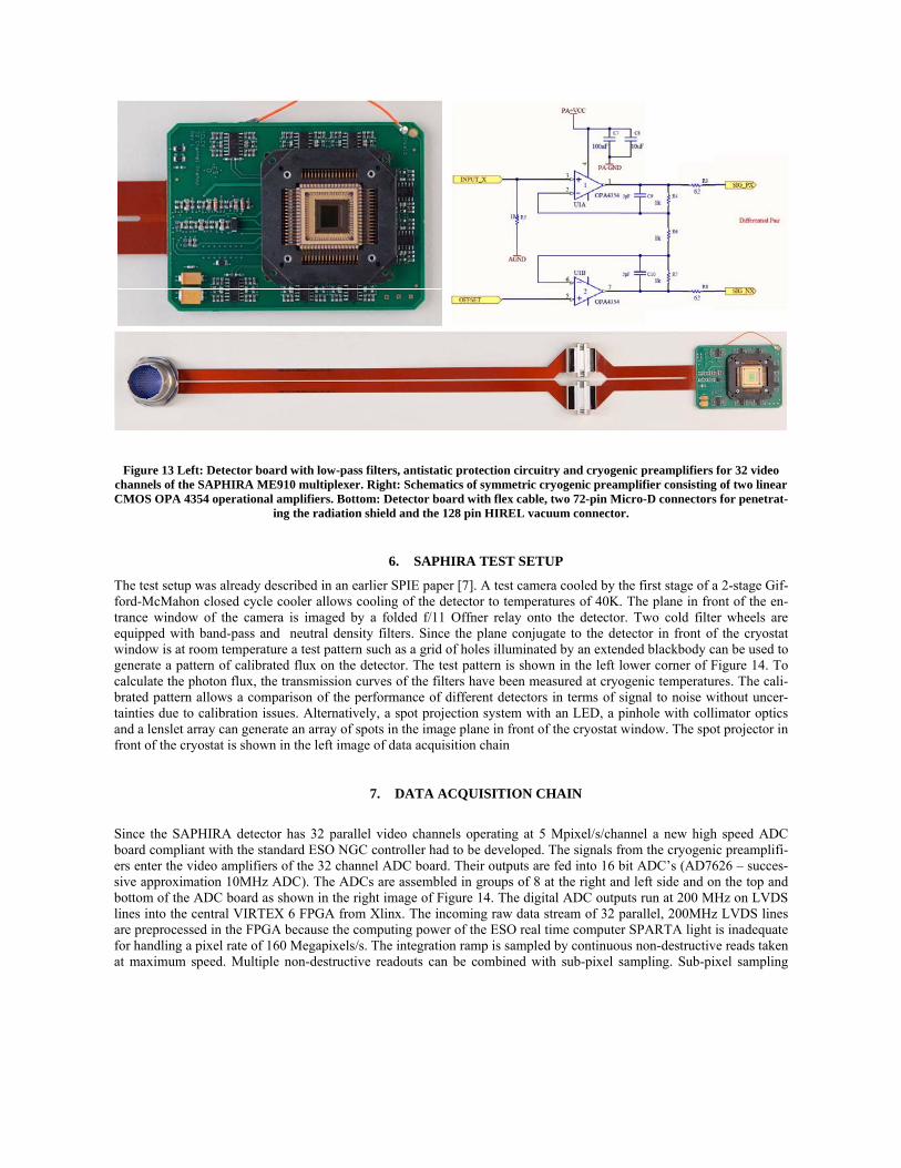
For the SAPHIRA array with 32 channels, the video outputs are amplified directly at the focal plane, on the detector board as shown in Figure 13. The robust and well proven symmetric preamplifier design used for the SWALLOW proto-type has been ported to the SAPHIRA detector. It was possible to integrate 64 preamplifiers into the same space con-straints defined by the original 4-channel SWALLOW preamplifier board, since a single IC is available which contains 4 op-amps which make up two channels. The preamplifier design matches the differential input stage of a newly developed 10 MHz, 32 channel ADC board which is described in chapter 0. The linear CMOS operational amplifier OPA4354 has a gain-bandwidth product of 100MHz and a noise of only 6.5nV/√Hz. It provides the required pixel speed of 5Mpixel/s/channel and operates reliably at cryogenic temperatures down to T=40K. The detector fan-out board with low-pass filters, antistatic protection and cryogenic preamplifiers is shown on the left side of Figure 13. N the right side is the schematics of the symmetric preamplifiers. The amplifier has a gain of x3. The inputs of the preamplifier are the video signal and an external reference voltage to compensate for the dc offset of the video signal. The outputs of the amplifier are two symmetric signals, SIG_PX and SIG_NX, which are routed through two flex boards and two 72-PIN Micro-D connectors, which penetrate the radiation shield and thermalise the flex-boards to the instrument temperature. In GRAV-ITY the optics of the Shack Hartmann wavefront sensor are cooled to liquid nitrogen temperature. From the radiation shield two 50 cm long flex-boards bring the signals to a single 128 pin HIREL hermetic connector and then via an exter-nal 4 meter long cable to the differential input stage of the ADC board in the NGC controller. The risetime and fall time of the video signal at the ADC input is ~ 80 ns. Symmetric amplification on the cold focal plane next to the detector makes the acquisition chain very robust and immune to noise pickup. However, there is a price to pay which is the increased power dissipation of 64 op-amps operating at 5 MHz (two per video output), next to the detector. The heat load of the preamplifiers in the present setup depends on the supply voltage of the op-amps. It can be decreased from 340 mW to 200mW by reducing the supply voltage from 4V to 3V. The power dissipation of the detector operating in the 32-channel mode at full speed and at high APD gain is only 150mW. A new revision of the detector board is in manufacture with special cooling planes for heat-sinking the dissipa-tion of the preamplifiers to the cold instrument. As far as possible the cooling power of the pulse tube should exclusively be reserved for cooling the detector.
Figure 13 Left: Detector board with low-pass filters, antistatic protection circuitry and cryogenic preamplifiers for 32 video channels of the SAPHIRA ME910 multiplexer. Right: Schematics of symmetric cryogenic preamplifier consisting of two linear CMOS OPA 4354 operational amplifiers. Bottom: Detector board with flex cable, two 72-pin Micro-D connectors for penetrat-
ing the radiation shield and the 128 pin HIREL vacuum connector.
6. SAPHIRA TEST SETUP
The test setup was already described in an earlier SPIE paper [7]. A test camera cooled by the first stage of a 2-stage Gif-ford-McMahon closed cycle cooler allows cooling of the detector to temperatures of 40K. The plane in front of the en-trance window of the camera is imaged by a folded f/11 Offner relay onto the detector. Two cold filter wheels are equipped with band-pass and neutral density filters. Since the plane conjugate to the detector in front of the cryostat window is at room temperature a test pattern such as a grid of holes illuminated by an extended blackbody can be used to generate a pattern of calibrated flux on the detector. The test pattern is shown in the left lower corner of Figure 14. To calculate the photon flux, the transmission curves of the filters have been measured at cryogenic temperatures. The cali-brated pattern allows a comparison of the performance of different detectors in terms of signal to noise without uncer-tainties due to calibration issues. Alternatively, a spot projection system with an LED, a pinhole with collimator optics and a lenslet array can generate an array of spots in the image plane in front of the cryostat window. The spot projector in front of the cryostat is shown in the left image of data acquisition chain
7. DATA ACQUISITION CHAIN
Since the SAPHIRA detector has 32 parallel video channels operating at 5 Mpixel/s/channel a new high speed ADC board compliant with the standard ESO NGC controller had to be developed. The signals from the cryogenic preamplifi-ers enter the video amplifiers of the 32 channel ADC board. Their outputs are fed into 16 bit ADC’s (AD7626 – succes-sive approximation 10MHz ADC). The ADCs are assembled in groups of 8 at the right and left side and on the top and bottom of the ADC board as shown in the right image of Figure 14. The digital ADC outputs run at 200 MHz on LVDS lines into the central VIRTEX 6 FPGA from Xlinx. The incoming raw data stream of 32 parallel, 200MHz LVDS lines are preprocessed in the FPGA because the computing power of the ESO real time computer SPARTA light is inadequate for handling a pixel rate of 160 Megapixels/s. The integration ramp is sampled by continuous non-destructive reads taken at maximum speed. Multiple non-destructive readouts can be combined with sub-pixel sampling. Sub-pixel sampling
means that more than one ADC conversion is made when a pixel is addressed. An average is then calculated which is equivalent to an analog low pass filter. This enables a very flexible user defined sampling scheme. The Fowler prepro-cessing of multiple non-destructive readouts in combination with sub-pixel sampling has been successfully tested with the SAPHIRA array. The ADC board has two 2.5 Gbit/s RocketI/O fiber transceivers which can also send the raw un-processed data stream to a newly developed PCIe interface board situated in a high end Linux pixel server PC with mul-ti-core CPUs. The interface to the AO WFS real time computer is a serial FPDP fiber link on the PCIe interface board.
Figure 14 Test rig for eAPD arrays. Left: Test camera IRATEC with spot projector and a lenslet array illuminating the image plane of detector in front of cryostat window. Middle: NGC high speed data acquisition system with Front end basic board and 32-channel ADC board. Right: 32-channel 10 MHz ADC board with VIRTEX-6 FPGA for real time high speed prepro-cessing of Fowler pairs with sub-pixel sampling.
8. SAPHIRA RESULTS
A major design effort was made to optimize the unit cell of the SAPHIRA ROIC in terms of sensitivity. A large low noise source follower with minimum gate capacitance was designed. The goal was to reduce both the noise voltage at the detector output and the gate capacitance of the source follower. A small capacitance at the integrating node increases the conversion gain in terms of Volt/electron. The first goal of lowering the noise floor was met as demonstrated by Figure 15. The noise histograms of the voltage measured at the detector outputs of the SWALLOW and the SAPHIRA ROICs are compared. The noise voltage of the SAPHIRA ROIC is 96 V, which is a factor of 3.3 lower than the noise voltage of 321 V measured with the SWALLOW ROIC. The transfer function of the SAPHIRA ROIC is 0.605, which is simi-lar to that measured for the SWALLOW device. The conversion gain was derived from the photon transfer curve by the same method as described in chapter 3. The conversion gain is 6.57 V/electron, at unity APD gain. This corresponds to a nodal capacitance of 24.3fF, which is in excellent agreement with the design value. Hence, the conversion gain of the SAPHIRA ROIC is a factor of 2.85 higher than the corresponding value of the SWALLOW prototype. The readout noise for single double correlated sampling is 30 e- rms, when reading out a 256x256 pixel window in 554 s. The main objec-tive of a low noise unit cell design is fully met by the SAPHIRA ROIC. The interpixel capacitance was checked by two methods. With the window reset method the capacitive coupling between pixels is directly measured in a similar way as with the single pixel reset method developed for the Hawaii-2RG array [8]. The array is uniformly illuminated with a large flux. During the stare time a small window is continuously reset. At
the edges of the reset window the coupling of the pixels adjacent to the reset window is measured. The coupling is < 2% as shown by the signal profile on the left side of Figure 16. The second method employs the autocorrelation calculated from a series of flat-field differences [9]. The autocorrelation of next neighboring pixels is caused by interpixel capacit-ance and is < 0.5% as shown on the right side of Figure 16. Therefore, the error of the conversion gain due to interpixel capacitance is < 2% when the variance instead of the integrated autocorrelation is used to derive the conversion gain from the photon transfer curve. At a temperature of 40K the conversion gain and the signal gain increase by exactly the same factor with increasing bias voltage. This is equivalent to an excess noise factor of 1. However, at T=80K the excess noise factor is 1.4 at high APD gain, possibly indicating some electrically active dislocations in the depletion region that are frozen out at lower temperature.
Figure 15 Noise comparison of of SAPHIRA ME910 ROIC and SWALLOW ME788 ROIC. APD gain=1. Noise at output of SAPHIRA ROIC: 96 V rms. Noise at output of SWALLOW ROIC: 321 V rms.
Figure 16 Interpixel capacitance of SAPHIRA array. Left: Capacitive coupling measured with the window reset method. Plot of trace through rest window. Capacitive coupling <2%. Right: Autocorrelation of next neighbors <0.5%
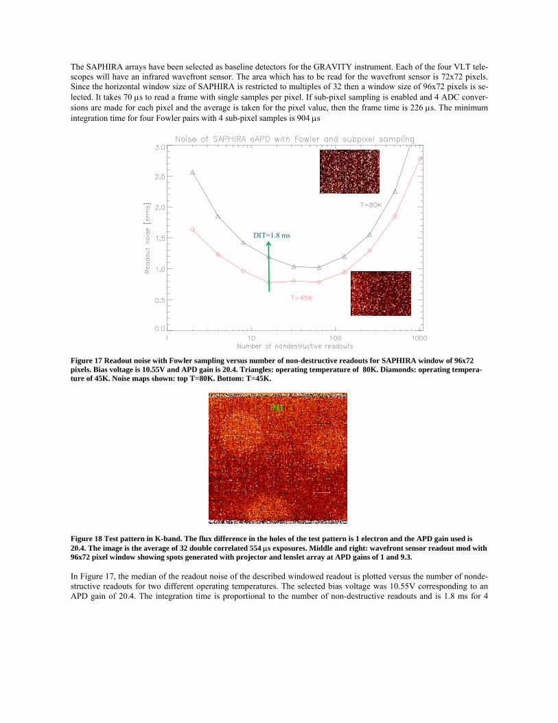
The SAPHIRA arrays have been selected as baseline detectors for the GRAVITY instrument. Each of the four VLT tele-scopes will have an infrared wavefront sensor. The area which has to be read for the wavefront sensor is 72x72 pixels. Since the horizontal window size of SAPHIRA is restricted to multiples of 32 then a window size of 96x72 pixels is se-lected. It takes 70 s to read a frame with single samples per pixel. If sub-pixel sampling is enabled and 4 ADC conver-sions are made for each pixel and the average is taken for the pixel value, then the frame time is 226 s. The minimum integration time for four Fowler pairs with 4 sub-pixel samples is 904 s
Figure 17 Readout noise with Fowler sampling versus number of non-destructive readouts for SAPHIRA window of 96x72 pixels. Bias voltage is 10.55V and APD gain is 20.4. Triangles: operating temperature of 80K. Diamonds: operating tempera-ture of 45K. Noise maps shown: top T=80K. Bottom: T=45K.
Figure 18 Test pattern in K-band. The flux difference in the holes of the test pattern is 1 electron and the APD gain used is 20.4. The image is the average of 32 double correlated 554 s exposures. Middle and right: wavefront sensor readout mod with 96x72 pixel window showing spots generated with projector and lenslet array at APD gains of 1 and 9.3. In Figure 17, the median of the readout noise of the described windowed readout is plotted versus the number of nonde-structive readouts for two different operating temperatures. The selected bias voltage was 10.55V corresponding to an APD gain of 20.4. The integration time is proportional to the number of non-destructive readouts and is 1.8 ms for 4
DIT=1.8 ms
Fowler pairs with an associated readout noise of 0.78 e-rms. Sub-electron readout noise is possible with the APD gain in combination with the described advanced sampling techniques. To further illustrate the potential of eAPDs, an average of 32 frames of 256x256 pixels taken with double correlated sampling, is shown in Figure 18. The pattern was taken with the grid of holes as described in chapter 6. The flux difference is 1 electron for an integration time of 554 s. The pattern is above the detection limit. On the right side of Figure 19, a 96x72 pixel wide windows shows the spots generated by a spot projector with a lenslet array at an APD gains of 1. On the left side the same exposure is shown with an APD gain of 9.3.
Figure 19 Wavefront sensor readout mod with 96x72 pixel sub-window showing spots generated with projector and lenslet array. Left: APD gain of 1. Right: APD gain of 9.3.
The first batch of SAPHIRA APD arrays were manufactured by SELEX to fully assess the ROIC and provide a baseline for the HgCdTe performance using the standard process. The SAPHIRA die size is larger than SWALLOW and this led to a thicker photoresist at the via-hole photolithographic stage. The resulting small via-hole caused a much smaller junc-tion diameter than normal. Unfortunately it is not possible to measure this without etching the surface and destroying the detector. The effect of a small junction diameter is that the depletion region is close to the crystal damage around the via-hole. Under high voltage bias the fields are locally excessive and create a hoste of undesirable effects, such as, early breakdown, noisy pixels and hot electron tunnelling into traps. The hot electron effects are reversible by removing the bias (zero bias cleaning) and annealing the array in vacuum at a temperature of 50C but the array degrades again when exposed to light. As a temporary measure each time the detector is reset, the bias voltage is first set to zero volts and then to the reverse bias voltage. To allow settling of the voltage levels an overhead of 50s has to be introduced for each re-set. On future batches of SAPHIRA the processing will be modified to drive the junction deeper. A new LPE array batch is expected within the next month with normal APD junction design.
9. PROTOTYPE EAPD ARRAYS USING THE MOVPE/MESA PROCESS
The MOVPE process is a wafer scale process with growth on a GaAs substrate and is now the standard FPA manufactur-ing process at SELEX, offering an intrinsically less expensive device than LPE. Compared with molecular beam epitaxy (MBE), MOVPE has a number of key strengths: the dopants are automatically activated during growth so there is no need to perform a high temperature post-growth anneal which may soften grades. There is also complete freedom to de-sign complex combinations of bandgaps and doping for the optimum performance. There are three more advantages of MOVPE compared with LPE. The MOVPE device structure is back-illuminated and so in eAPDs, short wavelength photons are absorbed high up in the structure and all of the photo-electrons can be swept to the avalanche region. It therefore has potentially the highest quantum efficiency for gain-multiplied carriers. Secondly, the device is based on mesa isolation of the pixels which gives near-ideal MTF and low crosstalk. Thirdly, the dark cur-rent can be two orders lower due to a much smaller absorber volume (factor of 6) compared with via-hole or planar structures and longer lifetime, extrinsically doped material.
A prototype batch of 2.5 µm MOVPE arrays has been recently manufactured to explore the breakdown characteristics, which was the main concern for MOVPE APD devices. This batch used a homojunction design to gain some compara-tive information on dark currents and quantum efficiency. The avalanche gain showed similar ionisation thresholds and exponents to LPE. The QE was measured to be 90% on gain-multiplied carriers which confirmed that the drift region efficiency was high. On the negative side, the dark current increased rapidly above 7V bias which probably reflected a higher dislocation density in this material growth system. Analysis showed that the dark current had trap-assisted tunne-ling (TAT) behaviour and originated around the junction region. A straightforward modification to reduce TAT currents is to widen the bandgap at the junction. This will be the subject of a future research program.
10. CONCLUSIONS
Using advanced sampling techniques sub-electron readout noise has been demonstrated with 320x256 pixel near infrared HgCdTe eAPD arrays on the new SAPHIRA ROIC which has been specifically developed for wavefront sensing and fringe tracking. The SAPHIRA ROIC has 32 parallel outputs with flexible window modes ideally matched to the needs of the VLTI instrument GRAVITY. In comparison to the SWALLOW ROIC the output noise voltage was reduced by a factor of 3.3and the conversion gain was increased by a factor of 2.8 to 6.57 V/electron at unity APD gain. This corres-ponds to a nodal capacitance of 24.3fF. Even though high sensitivity has been demonstrated with the SAPHIRA multip-lexer, recently delivered LPE arrays suffer from batch problems and exhibit non-uniform flat-fields at high APD gain, after exposure to light. It is desirable to get arrays with better cosmetic quality at high APD gain. Since the quality of arrays varies from batch to batch the growth technology has to mature further. A change from LPE to MOVPE is ex-pected to yield better quantum efficiency and lower dark current. More elaborate diode structures such as heterojunctions have the potential to combine low dark current, better cosmetics and high APD gain. Eventually, the avalanche gain may also become interesting for long exposures and improve the sensitivity of large science arrays.
REFERENCES
[1] Rothman J, Mollard L, Gout S et al, “History-Dependent Impact Ionisation Theory Applied to HgCdTe e-APDs”, Jn of Elec Mat, Vol 40, No 8, (2011).
[2] Kinch M.A, and Baker I.M, “HgCdTe Electron Avalanche Photodiodes”, Chapter 21, Mercury Cadmium Telluride - Growth, Properties and Applications, published by Wiley, (2011).
[3] Baker I.M, Crimes G.J, Parsons J.E. and O’Keefe E.S., “CdHgTe-CMOS hybrid focal plane arrays – a flexible solu-tion for advanced infrared systems”, Proc. SPIE, Vol 2269, p.636., (1994)
[4] Baker I.M. and Maxey C.D., “Summary of HgCdTe 2D array technology in the UK”, Jn. Elec. Mat, Vol 30, No.6, p.682, (2003).
[5] Hipwood L.G, Jones C.L, Shaw C, et al, “Affordable high-performance LW IRFPAs made from HgCdTe grown by MOVPE”, Proceedings of SPIE, 6206, 10-1, (2006).
[6] Hipwood L.G, Jones C.L, Walker D, et al., Proc. of SPIE, Vol 6542, 65420I, (2007). [7] Finger G., Baker I., Dorn R., Eschbaumer S., Ives D., Mehrgan L., Meyer,M., Stegmeier J., “Development of high-
speed, low-noise NIR HgCdTe avalanche photodiode arrays for adaptive optics and interferometry”, Proc. SPIE 7742, pp. 77421K (2010).
[8] Finger G., Garnett J., Bezawada N., Dorn R., Mehrgan L., Meyer M., Moorwood A., Stegmeier J., Woodhouse G., “Performance evaluation and calibration issues of large format infrared hybrid active pixel sensors used for ground- and space-based astronomy”, Nuclear Instruments and Methods in Physics Research Section A, Volume 565, Issue 1, pp. 241-250, (2006).
[9] Finger G., Meyer M., Mehrgan L., Moorwood A.F.M.; Stegmeier J., “Interpixel capacitance in large format CMOS hybrid arrays”, Proc. SPIE 6276E..62760F, (2006).
[10] Eisenhauer F. et al., “GRAVITY: Observing the Universe in Motion”, The Messenger, vol. 143, p. 16-24, (2011).