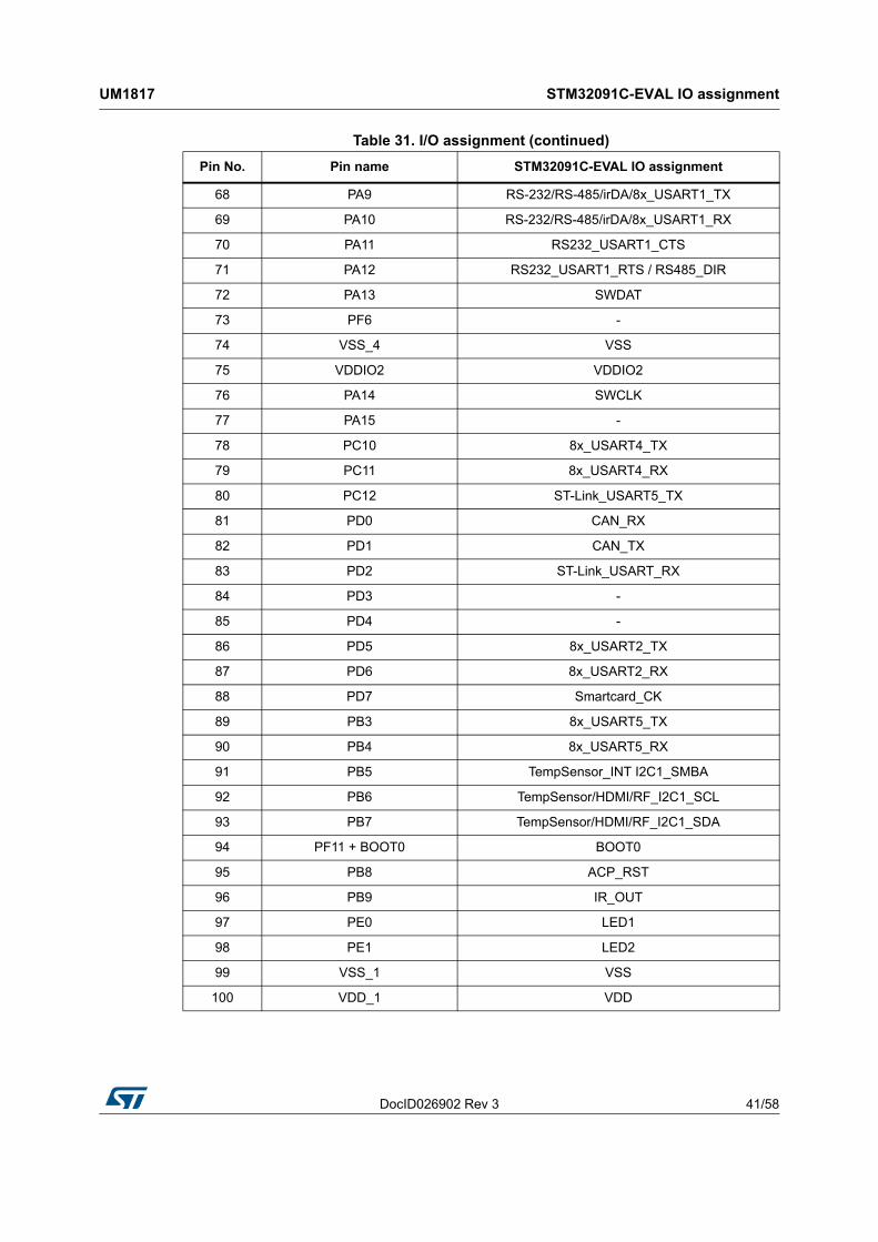
June 2016 DocID026902 Rev 3 1/58 1 UM1817 User manual Evaluation board with STM32F091VC MCU Introduction The STM32091C-EVAL evaluation board is designed as a complete demonstration and development platform for STMicroelectronics ARM ® Cortex ® -M0 core-based STM32F091VCT6 microcontroller, with two I 2 Cs, two SPIs, eight USARTs, one CAN, 12-bit ADC, 12-bit DAC, two GP comparators, internal SRAM and 256-Kbyte Flash memory , Touch sensing, CEC and SWD debugging support. The full range of hardware features on the board helps the user to evaluate all the peripherals (8x USARTs, RS-232, RS-485, Audio DAC, microphone ADC, Touch sensing buttons, TFT LCD, CAN, IrDA, IR LED, IR receiver, LDR, microSD card, CEC on two HDMI connectors, smartcard slot, RF-EEPROM and temperature sensor) and to develop applications. Extension headers make it possible to easily connect a daughterboard or wrapping board for a specific application. An ST-LINK/V2-1 is integrated on the board as an embedded in-circuit debugger and programmer for the STM32. Figure 1. STM32091C-EVAL evaluation board 1. Picture not contractual. www.st.com
Transcript
June 2016 DocID026902 Rev 3 1/58
1
UM1817User manual
Evaluation board with STM32F091VC MCU
Introduction
The STM32091C-EVAL evaluation board is designed as a complete demonstration and development platform for STMicroelectronics ARM® Cortex®-M0 core-based STM32F091VCT6 microcontroller, with two I2Cs, two SPIs, eight USARTs, one CAN, 12-bit ADC, 12-bit DAC, two GP comparators, internal SRAM and 256-Kbyte Flash memory, Touch sensing, CEC and SWD debugging support.
The full range of hardware features on the board helps the user to evaluate all the peripherals (8x USARTs, RS-232, RS-485, Audio DAC, microphone ADC, Touch sensing buttons, TFT LCD, CAN, IrDA, IR LED, IR receiver, LDR, microSD card, CEC on two HDMI connectors, smartcard slot, RF-EEPROM and temperature sensor) and to develop applications. Extension headers make it possible to easily connect a daughterboard or wrapping board for a specific application. An ST-LINK/V2-1 is integrated on the board as an embedded in-circuit debugger and programmer for the STM32.
• STM32F091VCT6 microncontroller with 256-Kbyte Flash memory and 32-Kbyte RAM
• Three 5 V power supply options: power jack, ST-LINK/V2-1 USB connector or daughterboard
• Stereo audio jack which supports headset with microphone connected to DAC and ADC of the STM32F091VCT6
• 2-Gbyte (or more) SPI interface microSD card
• I2C compatible serial interface temperature sensor
• RF-EEPROM
• RS-232 and RS-485 communication
• IrDA transceiver
• IR LED and IR receiver
• SWD debug support, ST-LINK/V2-1 embedded
• 240x320 TFT color LCD connected to SPI interface of STM32F091VCT6
• Joystick with 4-direction control and selector
• Reset, Tamper and user-buttons
• 4-color user LEDs and two LEDs as STM32 low-power alarm
• Extension connector for daughterboard or wrapping board
• STM32 voltage choice fixed 3.3 V or adjustable from 1.65 V to 3.6 V
• Touch sensing buttons
• RTC with backup battery
• CAN2.0A/B compliant connection
• Light dependent resistor (LDR)
• Potentiometer
• Two HDMI connectors with DDC and CEC
• Smartcard slot
• 8x USARTs chain connector
1.2 Demonstration software
Demonstration software is preloaded in the STM32F091VCT6 Flash memory for easy demonstration of the device peripherals in stand-alone mode. For more information and to download the latest version available, refer to the STM32091C-EVAL demonstration software available on the www.st.com website.
1.3 Order code
To order the evaluation board for the STM32F091VCT6 MCU, use the order code STM32091C-EVAL.
DocID026902 Rev 3 7/58
UM1817 Overview
57
1.4 Delivery recommandations
Before using the board for the first time, the user should check that it has not been visibly damaged during the shipment, and that no components are unplugged or missing.
When the board is extracted from its plastic bag, check that no component remains in the bag.
The main components to verify are:
1. The 8 MHz crystal (X2) which may have been removed from its socket by a shock.
2. The microSD card which may have been ejected from the CN8 connector (right side of the board).
3. The dual-interface EEPROM board (ANT7-M24LR-A) which may have been unplugged from the CN2 connector (top left corner of the board).
For all information concerning the version of the MCU used on the board, its specification and possible related limitations, visit the ST web site www.st.com to download relevant datasheet and errata sheet.
Hardware layout and configuration UM1817
8/58 DocID026902 Rev 3
2 Hardware layout and configuration
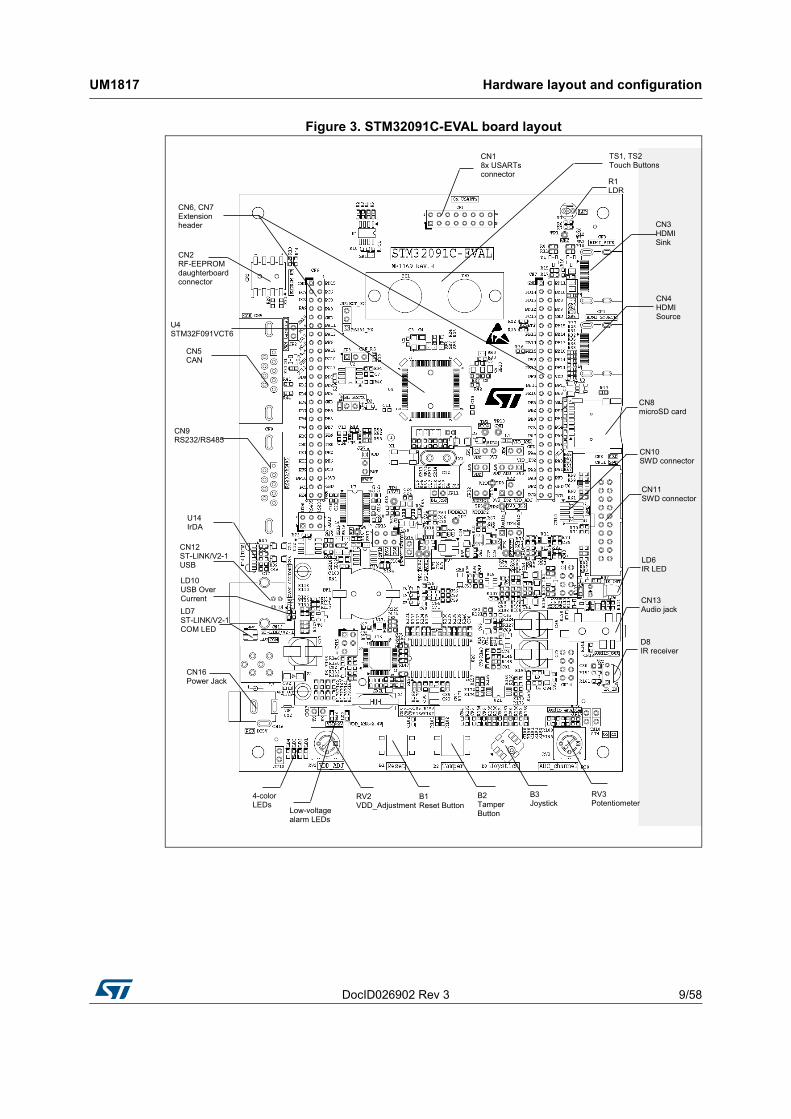
The STM32091C-EVAL evaluation board is designed around the STM32F091VCT6 (100-pin LQFP package). The hardware block diagram Figure 2 illustrates the connection between the STM32F091VCT6 and the peripherals (8x USARTs, RS-232, RS-485, Audio DAC, microphone ADC, Touch sensing buttons, TFT LCD, CAN, IrDA, IR LED, IR receiver, LDR, microSD card, CEC on two HDMI connectors, smartcard slot, RF-EEPROM and Temperature sensor) and Figure 3 helps the user to locate these features on the actual evaluation board. The Figure 4 and the Table 1 show the board mechanical dimensions.
Figure 2. Hardware block diagram
DocID026902 Rev 3 9/58
UM1817 Hardware layout and configuration
57
Figure 3. STM32091C-EVAL board layout
CN2 RF EEPROMdaughterboardconnector
CN3 HDMI Sink
CN12 ST-LINK/V2-1 USB
CN11 SWD connector
CN13 Audio jack LD7
ST-LINK/V2-1 COM LED
B2 Tamper Button
B1 Reset Button
4 colorLEDs
RV3 Potentiometer
RV2VDD_Adjustment
CN16 Power Jack
U14 IrDA
U4 STM32F091VCT6
CN6, CN7 Extension header
CN10 SWD connector
CN18x USARTs connector
CN4 HDMI Source
D8IR receiver
LD6 IR LED
CN8 icroSD card
B3 Joystick
CN9 RS232/RS485
TS1, TS2 Touch Buttons
Low voltagealarm LEDs
CN5 CAN
R1 LDR
LD10 USB Over Current
Hardware layout and configuration UM1817
10/58 DocID026902 Rev 3
Figure 4. Mechanical dimensions
Table 1. Mechanical dimensions
Symbol Size (mm) Symbol Size (mm) Symbol Size (mm)
A 68.58 e 77.44 P1 26.67
a1 2.54 H 11 P2 111.76
a2 2.54 Lx 5.715 Q1 24.12
B 36 Ly 5.715 Q2 17.70
D 3.5 Mx 19.08 X 114.3
d 3.2 My 23.81 Y 172.72
DocID026902 Rev 3 11/58
UM1817 Hardware layout and configuration
57
2.1 Embedded ST-LINK/V2-1
The ST-LINK/V2-1 programming and debugging tool is integrated on the STM32091C-EVAL evaluation board. Compared to ST-LINK/V2 the changes are listed below.
The new features supported on ST-LINK/V2-1 are:
• USB software re-enumeration
• Virtual COM port interface on USB
• Mass storage interface on USB
• USB power management request for more than 100 mA power on USB
This feature is no more supported on ST-LINK/V2-1:
• SWIM interface
For all general information concerning debugging and programming features common between V2 and V2-1 refer to the ST-LINK/V2 in-circuit debugger/programmer for STM8 and STM32ST-LINK/V2 User manual (UM1075).
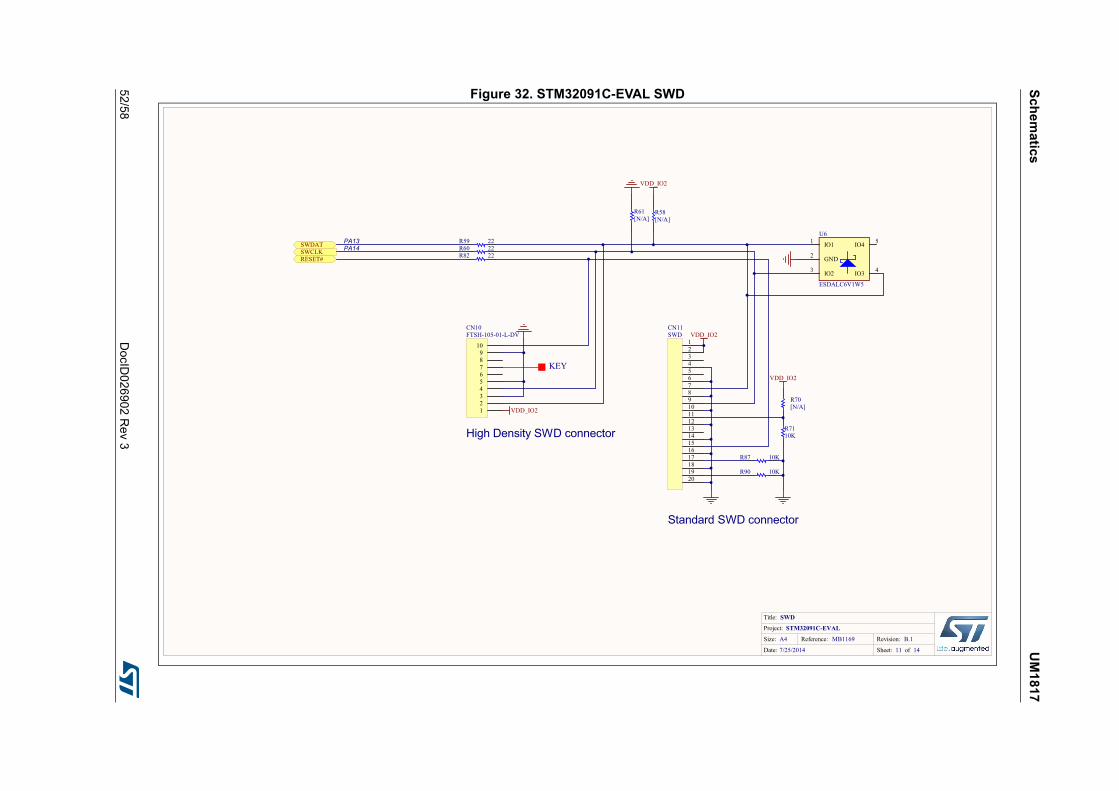
Note: It is possible to power the board via CN12 (Embedded ST-LINK/V2-1 USB connector) even if an external tools is connected to CN10 (High density SWD connector) or CN11 (SWD connector).
2.1.1 Drivers
The ST-LINK/V2-1 requires a dedicated USB driver, which can be found at the www.st.com website for Windows® 7 and 8. On Windows® XP the ST-LINK/V2-1 driver requires WinUsb to be installed before using the ST-LINK/V2-1 (either available from Microsoft website or included in the USB driver for ST-LINK/V2 for XP).
In case the STM32091C-EVAL evaluation board is connected to the PC before the driver is installed, some STM32091C-EVAL interfaces may be declared as “Unknown” in the PC device manager. In this case the user must install the driver files, and update the driver of the connected device from the device manager.
Note: Prefer using the “USB Composite Device” handle for a full recovery.
Figure 5. USB Composite Device
Hardware layout and configuration UM1817
12/58 DocID026902 Rev 3
2.1.2 ST-LINK/V2-1 firmware upgrade
The ST-LINK/V2-1 embeds a firmware upgrade mechanism for in-situ upgrade through the USB port. As the firmware may evolve during the life time of the ST-LINK/V2-1 product (for example new functionalities, bug fixes, support for new microcontroller families), it is recommended to visit the www.st.com website before starting to use the STM32091C-EVAL board and periodically, in order to stay up-to-date with the latest firmware version.
2.2 Board power supply
STM32091C-EVAL evaluation board is designed to be powered by 5 V DC power supply and to be protected by PolyZen from wrong power plug-in event. It is possible to configure the evaluation board to use any of the following three sources for the power supply:
• 5 V DC power adapter connected to CN16 (the Power jack on the board showed as PSU on JP15 silkscreen and called E5V). The external power supply is not provided with the board.
• 5 V DC power from CN12 (the USB Type-B connector of ST-LINK/V2-1, that is showed as STlk on JP15 silkscreen and called U5V). If the USB enumeration succeeds (as explained below), the ST-LINK U5V power is enabled, by asserting the PWR_EN pin. This pin is connected to a power switch (ST890), which powers the board. This power switch features also a current limitation to protect the PC in case of short-circuit on the board. If overcurrent (more than 600 mA) happens on board, the LED LD10 is lit.
• 5 V DC power from CN7 (the extension connector for daughterboard, that is showed as D5V on JP15 silkscreen).
STM32091C-EVAL evaluation board can be powered from ST-LINK USB connector CN12 (U5V), but only the ST-LINK part has the power before USB enumeration, because the host PC only provides 100 mA to the board at that time. During the USB enumeration, the STM32091C-EVAL board asks for the 300 mA power to the host PC. If the host is able to provide the required power, the enumeration finishes by a “SetConfiguration” command and then, the power transistor U23 (ST890) is switched ON, the red LED LD5 is turned ON, thus STM32091C-EVAL board can consume maximum 300 mA current, but not more. If the host is not able to provide the requested current, the enumeration fails. Therefore the ST890 (U23) remains OFF and the STM32 part including the extension board will not be powered. As a consequence the red LED LD5 remains turned OFF. In this case it is mandatory to use an external power supply as extra power supply.
E5V (from PSU) or D5V can be used as external power supply in case the current consumption of the STM32091C-EVAL board exceeds the allowed current on the USB. In this condition it is still possible to use the USB for communication, for programming or debugging only, but it is mandatory to power the board first using E5V or D5V, then connecting the USB cable to the PC. Proceeding this way the enumeration succeeds thanks to the external power source.
The following power sequence procedure must be respected:
4. Connect jumper JP15 for PSU or D5V side
5. Check that JP18 is removed
6. Connect the external power source to PSU or D5V (daughterboard mounted)
7. Check red LED LD5 is turned ON
8. Connect the PC to USB connector CN12
DocID026902 Rev 3 13/58
UM1817 Hardware layout and configuration
57
If this order is not respected, the board may be powered by VBUS first then E5V or D5V, and the following risks may be encountered:
1. If more than 300 mA current is needed by the board, the PC may be damaged or current can be limited by PC. As a consequence the board is not powered correctly.
2. 300 mA is requested at enumeration (since JP18 must be OFF), so there is risk that the request is rejected and the enumeration does not succeed if the PC cannot provide such current. Consequently the board is not powered (LED LD5 remains OFF).
Note: In case the board is powered by a USB charger, there is no USB enumeration, so the led LD5 remains set to OFF permanently and the board is not powered. Only in this specific case the jumper JP18 needs to be set to ON, to allow the board to be powered anyway.
Figure 6 helps to understand the structure of the power source on the evaluation board.
Figure 6. Structure of the power source
The power source is selected by setting the related jumpers JP15, JP7 and JP10 as described in Table 2.
Hardware layout and configuration UM1817
14/58 DocID026902 Rev 3
Table 2. Power source related jumpers
Jumper Description
JP15
JP15 is used to select one of the three possible power supply resources. For power supply jack (CN16) to the STM32091C-EVAL only, JP15 is set as shown to the right:
For power supply from the daughterboard connectors (CN7) to STM32091C-EVAL only, JP15 is set as shown to the right:
For power supply from USB (CN12) of ST-LINK/V2-1 to STM32091C-EVAL only, JP15 is set as shown to the right: (Default Setting)
For power supply from power supply jack (CN16) to both STM32091C-EVAL and daughterboard connected on CN6 and CN7, JP15 is set as shown to the right (daughterboard must not have its own power supply connected)
JP7
The Vbat pin of STM32F091VCT6 is connected to VDD when JP7 is set as shown to the right (Default setting):
The Vbat pin of STM32F091VCT6 is connected to the 3 V battery when JP7 is set as shown to the right:
JP10
The VDDIO2 pin of STM32F091VCT6 is connected to 3.3V when JP10 is set as shown to the right (Default setting):
The VDDIO2 pin of STM32F091VCT6 is connected to VDD_ADJ when JP10 is set as shown to the right:
PSU
D5V
STlk
PSU
D5V
STlk
PSU
D5V
STlk
PSU
D5V
STlk
1 2 3
1 2 3
1 2 3
1 2 3
DocID026902 Rev 3 15/58
UM1817 Hardware layout and configuration
57
2.3 STM32 power-mode configuration
Total three power modes are supported on the board that are configured by setting the related jumpers JP5, JP6, JP8, JP9 and JP12 as described in Table 3 and in the Notes below.
• Mode1: The VDD and VDDA are connected together and powered by fixed 3.3 V.
• Mode2: The VDD and VDDA are connected together and powered by adjustable voltage from 1.65 V to 3.6 V.
• Mode3: The VDD is powered by adjustable voltage from 1.65 V to 3.6 V while VDDA is powered by fixed 3.3 V.
Note:1 JP8 allows current measurement on VDD_MCU. Current measurement is performed by replacing JP8 by an ammeter.
Note:2 JP12 allows current measurement on VDDIO2. Current measurement is performed by replacing JP12 by an ammeter.
Note:3 JP6 allows to connect analog power source VDD_ANA to the STM32 VDDA. JP6 must be opened (to disconnect VDDA from all analog power VDD_ANA which is connected to analog circuits on the board) for STM32 Idd measurement.
Note:4 LD8 is lit when VDD < 2V and in this case STM32 is not functional. LD9 is lit when VDDA < 2.4 V and in this case analogue parts in STM32F091VCT6 are not functional.
The LED LD5 is lit when the STM32091C-EVAL evaluation board is powered by the 5 V correctly.
Table 4 shows the low-voltage limitations that might apply depending on the characteristics of some peripheral components. Components might work incorrectly when the power level is lower than the limitation.
Table 3. Power mode related jumpers
Power modePower mode configuration VDD_MCU Idd
measurement (On JP8)JP9 JP5
Mode1
OK
NOT allowed
Mode2 OK
Mode3 NOT allowed
1 2 3 1 2 3
1 2 3 1 2 3
1 2 3 1 2 3
1 2 3 1 2 3
Hardware layout and configuration UM1817
16/58 DocID026902 Rev 3
CAUTION:
1. JP8 and JP12 are not allowed to be opened; otherwise STM32F091VCT6 would be damaged due to a lack of power supply on its power pins.
2. Risk of explosion if battery is replaced by an incorrect type. Dispose of used batteries according to the instructions.
2.4 Clock source
Two clock sources are available on the STM32091C-EVAL evaluation board for STM32F091VCT6 and RTC embedded.
• X1, 32 KHz crystal for embedded RTC
• X2, 8 MHz crystal with socket for STM32F091VCT6 microcontroller, it can be removed from socket when internal RC clock is used.
See Table 5 and Table 6.
Table 4. Low-voltage limitation
Peripheral Component IO name Low-voltage limitation
Audio amplifier U18 Audio input 2.2 V (VDDA)
Microphone amplifier U15 Audio output 2.7 V (VDDA)
CAN CN5 CAN 3 V (VDDIO2)
Smartcard CN19 USART2 2.7 V (VDD)
Table 5. 32 KHz crystal X1 related solder bridges
Jumper Description
SB11
PC14 is connected to the 32KHz crystal when SB11 is open.
(Default setting)
PC14 is connected to extension connector CN6 when SB11 is closed. In such case R54 must be removed to avoid disturbance due to the 32 Khz quartz.
SB12
PC15 is connected to the32 KHz crystal when SB12 is open.
(Default setting)
PC15 is connected to extension connector CN6 when SB12 is closed. In such case R55 must be removed to avoid disturbance due to the 32 Khz quartz.
Table 6. 8MHz crystal X2 related solder bridges
Jumper Description
SB13
PF0 is connected to the 8 MHz crystal when SB13 is open.
(Default setting)
PF0 is connected to the extension connector CN7 when SB13 is closed. In such case C18 and X2 must be removed.
DocID026902 Rev 3 17/58
UM1817 Hardware layout and configuration
57
2.5 Reset source
The reset signal of STM32091C-EVAL evaluation board is low active and the reset sources include:
• Reset button B1
• Debugging tools from SWD connector CN10 and CN11
• Daughterboard from CN7
• Embedded ST-LINK/V2-1
• RS-232 connector CN9 for ISP.
Note: The jumper JP11 must be closed for RESET handled by pin 8 of the RS-232 connector CN9 (CTS signal). Refer to Section 2.8 for details.
2.6 Boot option
The STM32091C-EVAL evaluation board is able to boot from:
• Embedded user Flash
• System memory with boot loader for ISP
• Embedded SRAM for debugging
The boot option is configured by setting one jumper cap on CN7 between pin 22 and pin 24 and one option bit (see Table 7).
The BOOT0 can also be configured via RS-232 connector CN9, as shown in Table 8.
SB14
PF1 is connected to 8MHz crystal when SB14 is open.
(Default setting)
PF1 is connected to extension connector CN7 when SB14 is closed. In such case R56 must be removed to avoid disturbance due to the 8 Mhz quartz.
Table 6. 8MHz crystal X2 related solder bridges (continued)
Table 7. Boot related switch
Switch configuration
bit12 in USER OPTION BYTES
Boot from
CN7 pin 22 and pin 24 opened
X STM32091C-EVAL boot from User Flash. (Default setting)
CN7 pin 22 and pin 24 closed by jumper
0 STM32091C-EVAL boot from Embedded SRAM.
CN7 pin 22 and pin 24 closed by jumper
1 STM32091C-EVAL boot from System Memory.
Hardware layout and configuration UM1817
18/58 DocID026902 Rev 3
2.7 Audio
STM32091C-EVAL evaluation board supports stereo audio playback and microphone recording by an external headset connected on audio jack CN13. Audio play is connected to DAC output of the STM32F091VCT6 through an audio amplifier and microphone on headset is connected to ADC input of the STM32F091VCT6 through a microphone amplifier. Audio amplifier is enabled or disabled by setting JP17 and mono/stereo playback is selected by setting JP14, refer to Table 9 for details.
Audio amplifier operates correctly when VDDA > 2.2V and microphone amplifier operates correctly when VDDA > 2.7V.
2.8 RS-232, RS-485 and IrDA
The RS-232 (with hardware flow control CTS and RTS), the RS-485 and the IrDA communication are supported by the D-type 9-pins RS-232/RS-485 connectors CN9, and by the IrDA transceiver U14 which is connected to the USART1 of the STM32F091VCT6 on the STM32091C-EVAL evaluation board. The signal Bootloader_RESET (shared with CTS signal) and the Bootloader_BOOT0 (shared with DSR signal) are added on the RS-232 connector CN9 for ISP support.
USART1_Rx is chosen by setting of JP13, refer to Table 10 for details.
Table 8. Boot0 related jumpers
Jumper Description
JP4
The Bootloader_BOOT0 is managed by pin 6 of the connector CN9 (RS-232 DSR signal) when JP4 is closed. This configuration is used for the bootloader application only.
Default Setting: Not fitted
Table 9. Audio related jumpers
Jumper Description
JP17Speaker amplifier U18 is enabled when JP17 is closed (Default setting)
Speaker amplifier U18 is disabled when JP17 is open
JP14
Mono playback is enabled when JP14 is set as shown to the right (Default setting):
Stereo playback is enabled when JP14 is set as shown to the right:
1 2 3
1 2 3
DocID026902 Rev 3 19/58
UM1817 Hardware layout and configuration
57
The RS-485 communication is supported by the RS-485 transceiver ST3485EBDR which is connected to pin 4 and pin 9 of D-type 9-pins connectors CN9 (share same connector with USART1), see Table 11.
2.9 Touch sensing buttons
Two touch sensing buttons are supported on the STM32091C-EVAL evaluation board and they are connected to three capacitive sensing channels (PD[12:14]) in group8 with active shield being connected to two capacitive sensing channels (PB11 and PB12) in group6 (see Table 12).
Table 10. RS-232 and IrDA related jumpers
Jumper Description
JP13
RS232_RX is connected to RS-232 transceiver and RS-232 communication is enabled when JP13 is set as shown to the right (Default setting):
RS485_RX is connected to RS-485 transceiver and RS-485 communication is enabled when JP13 is set as shown to the right:
IrDA_RX is connected to IrDA transceiver and IrDA communication is enabled when JP13 is set as shown to the right:
Table 11. RS-485 related solder bridges
Jumper Description
SB15, SB18The external failsafe biasing are enabled when solder bridges SB15 and SB18 are closed
Default Setting: Not fitted
SB19The bus termination is enabled when solder bridge SB19 is closed.
Default Setting: Not fitted
SB16The AC termination is disabled when solder bridge SB16 is closed for high baud rate communication.
Default Setting: Not fitted
RS232
RS485
IrDA
RS232
RS485
IrDA
RS232
RS485
IrDA
Hardware layout and configuration UM1817
20/58 DocID026902 Rev 3
Note: Touch sensing buttons are fully functional only when the STM32091C-EVAL board is powered on in power mode 1 (both VDD and VDDA are connected to fixed 3.3 V). It is potentially necessary to adjust the capacitor value of C8 and the firmware to adapt them to the voltage range from 1.65 V to 3.6 V of VDD on power-mode 2 and 3.
2.10 microSD card
The 2-Gbyte (or more) microSD card connected to SPI1 port (Shared with color LCD) of the STM32F091VCT6 is available on the board. microSD card detection is managed by standard IO port PE11 and it should be set with internal pull-up.
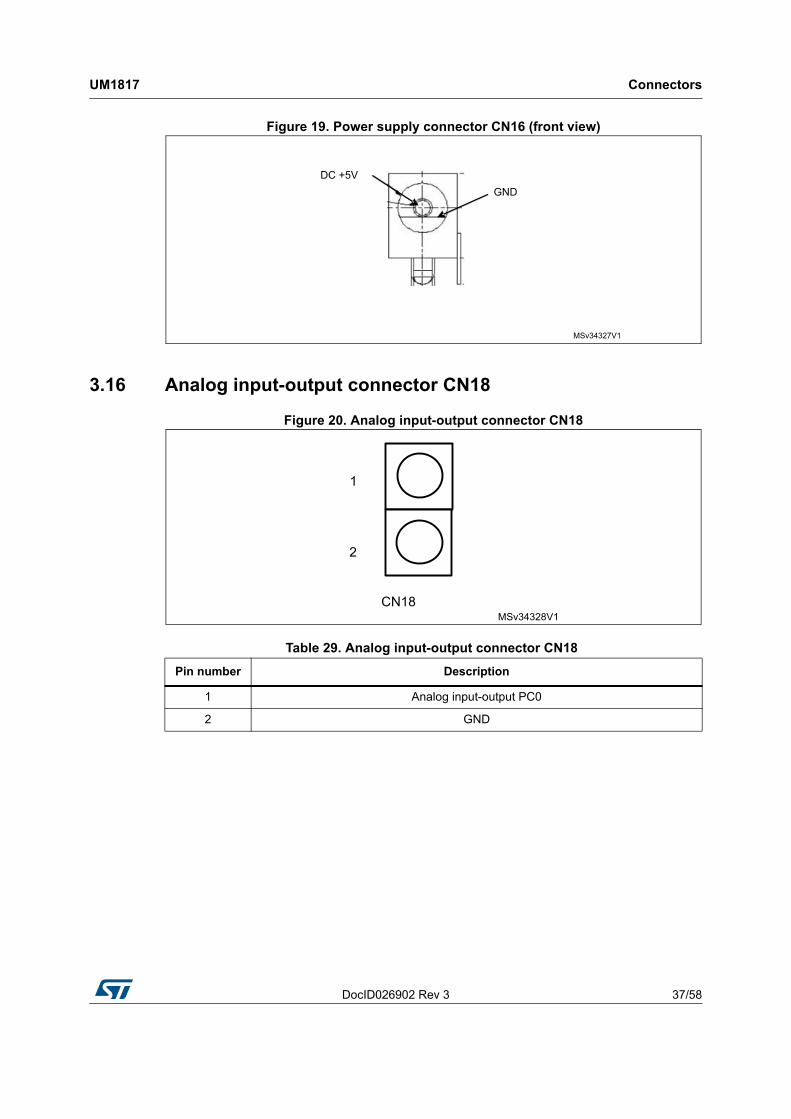
2.11 Analog input
The two-pin header CN18 and the 10K ohm potentiometer RV3 are connected to PC0 of STM32F091VCT6 as analog input. A low-pass filter is implemented by replacing R191 and C101 with the right value of resistor and capacitor as requested by end user’s application.
Table 12. Touch sensing buttons related solder bridges
Solder Bridge Description
SB7
PD13 is connected to touch slider when SB7 is open.
(Default setting)
PD13 is connected to extension connector CN7 when SB7 is closed. In such case R24 must be removed to avoid disturbance due to the touch button.
SB8
PD12 is connected to touch slider when SB8 is open.
(Default setting)
PD12 is connected to extension connector CN7 when SB8 is closed. In such case R25 must be removed to avoid disturbance due to the touch button.
SB6
PD14 is connected to sampling capacitor when SB6 is open.
(Default setting)
PD14 is connected to extension connector CN7 when SB6 is closed. In such case C4 must be removed to avoid disturbance due to the capacitor.
SB9
PB12 is connected to shield when SB9 is open.
(Default setting)
PB12 is connected to extension connector CN6 when SB9 is closed. In such case R30 must be removed to avoid disturbance due to the shield.
SB10
PB11 is connected to shield charge capacitor when SB10 is open.
(Default setting)
PB11 is connected to extension connector CN6 when SB10 is closed. In such case R37 must be removed to avoid disturbance due to the capacitor.
DocID026902 Rev 3 21/58
UM1817 Hardware layout and configuration
57
2.12 LDR (Light Dependent Resistor)
The VDDA is divided by resistor bridge of LDR VT9ON1 and 8.2K resistor and connected to PA1 (COM1_IN+/ADC IN1) as shown below in Figure 7 on the STM32091C-EVAL evaluation board.
Figure 7. GP comparator 1
It is possible to compare LDR output with 1/4 band gap, 1/2 band gap, 3/4 band gap, band gap and DAC1 OUT and to connect LDR output to ADC IN1 for AD conversion.
2.13 Temperature sensor
A temperature sensor STLM75M2F is connected to I2C1 bus of the STM32F091VCT6, and share same I2C1 bus with RF-EEPROM and DDC on HDMI_Source connector CN4.
I2C address of temperature sensor is 0b100100 (A0), A0 can be 0 or 1, depending on the setting of SB1, see Table 13.
Hardware layout and configuration UM1817
22/58 DocID026902 Rev 3
Note: The temperature result measured from STLM75M2F would be a little higher than the ambient temperature due to the power dissipation of the components on the board.
2.14 Smartcard
STMicroelectronics smartcard interface chip ST8024L is used on the STM32091C-EVAL evaluation board for asynchronous 1.8 V, 3 V and 5 V smartcards. It performs all supply protection and control functions based on the connections with the STM32F091VCT6 listed in Table 14.
Smartcard operates correctly when VDD > 2.7 V.
2.15 CAN
STM32091C-EVAL evaluation board supports one channel of CAN2.0A/B compliant CAN bus communication based on 3.3 V CAN transceiver. The high-speed mode, standby mode and slope-control mode are available and selectable by setting JP3 (see Table 15).
Table 13. Temperature sensor or related solder bridge
Solder Bridge Description
SB1
I2C address A0 is 0 when SB1 is open
(Default setting)
I2C address A0 is 1 when SB1 is closed.
Table 14. Connection between ST8024L and STM32F091VCT6
Signals of ST8024L Description Connect to STM32F091VCT6
1.8 V VCC operation selection. Logic high selects 1.8 V operation and overrides any setting on the 5 V/3 V pin.
PC1
DocID026902 Rev 3 23/58
UM1817 Hardware layout and configuration
57
CAN operates correctly when VDDIO2 > 3V.
2.16 RF-EEPROM
A RF-EEPROM module ANT7-M24LR-A is mounted on connector CN2 and connected to I2C1 bus of the STM32F091VCT6, this bus shares same I2C1 bus with the temperature sensor U1 and DDC on HDMI_Source connector CN4.
The I2C address of the RF-EEPROM daughterboard is 0b1010000.
2.17 HDMI CEC
Two HDMI connectors CN3 and CN4 are available on the STM32091C-EVAL board.
• The connector CN3 is HDMI sink connector with:
– DDC connected to I2C2 of the STM32F091VCT6
– HPD controlled by I/O PD11 through transistor T1
– CEC connected to PB10 through transistor T2
• The connector CN4 is HDMI source connector with:
– DDC connected to I2C1 of the STM32F091VCT6 and shared with the temperature sensor and RF-EEPROM
– HPD controlled by I/O PD10
– CEC connected to PB10 through transistor T2
– HDMI 5 V powered by power switch U3
The signals TDMS D+[0..2], TDMS_CLK+, TDMS D-[0..2], TDMS_CLK- on these two HDMI connectors are connected together.
The CEC injector mode is enabled by some PCB reworks for debugging purpose only:
Note: The I/O PD11 must be set in open-drain output mode by firmware when working as an HPD signal control on the HDMI sink connector CN3.
Table 15. CAN related jumpers
Jumper Description
JP3
CAN transceiver is working in standby mode when JP3 is set as shown to the right:
CAN transceiver is working in high-speed mode when JP3 is set as shown to the right: (default setting)
CAN transceiver is working in slope-control mode when JP3 is open.
JP2CAN terminal resistor is enabled when JP2 is fitted.
Default setting: Not fitted
1 2 3
1 2 3
Hardware layout and configuration UM1817
24/58 DocID026902 Rev 3
2.18 IR LED and IR receiver
The IR receiver TSOP34836 is connected to PC6 of the STM32F091VCT6 and a current around 100 mA on IR LED is driven by PB9 through transistors T4 and T5 on the board.
Note: The IR LED may be driven by PB9 directly with 20 mA current when SB20 is closed and R116 is removed.
2.19 8x USARTs
USART chain could be routed to a 2*8 header so that some jumpers could be used to connect them to demonstrate 8x USART channels in daisy chain.The data flow is showed in the below Figure 8.
Figure 8. USART data flow
At the end both data sent at USART1_TX and data received at USART_RX can be compared and validated thanks to USARTs chain on CN1.
Warning: USART1/4/8 belongs to VDDIO2 power domain and USART2/3/5/6/7 belongs to VDDIO power domain, so the same voltage level for VDDIO and VDDIO2 is needed, to demonstrate USART chain application on this header.
2.20 Display and input devices
The 2.4” color TFT LCD connected to SPI1 port of the STM32F091VCT6 and 4-general- purpose-color LEDs (LD 1,2,3,4) are available as display device. The 4-direction joystick (B3) with selection key, which connects to PA0 and supports wakeup feature, and Tamper button (B2) are also available as input devices (see Table 16).
USART1_TX USART2_RX
USART2_TX USART3_RX
USART3_TX USART4_RX
USART4_TX USART5_RX
USART5_TX USART6_RX
USART6_TX USART7_RX
USART7_TX USART8_RX
USART8_TX USART1_RX
DocID026902 Rev 3 25/58
UM1817 Hardware layout and configuration
57
Note: The bi-directional voltage translator is implemented on SPI MOSI signal between the STM32F091VCT6 and the LCD to support 3-wires serial interface for various voltage level interface. The direction of this voltage translator is controlled by I/O PE9 (the I/O PE15 is working as MOSI when PE9 is high or as MISO when PE9 is LOW).
1,3,4,6,7,9,10,12TMDS differential signal pair connected to CN4
16 I2C2_SDA (PB14)
13 CEC (PB10) 2,5,8,11,17 GND
14 NC 18 HDMI_5V_Sink
15 I2C2_SCL (PB13) 19HPD (PD11 through
transistor)
Connectors UM1817
28/58 DocID026902 Rev 3
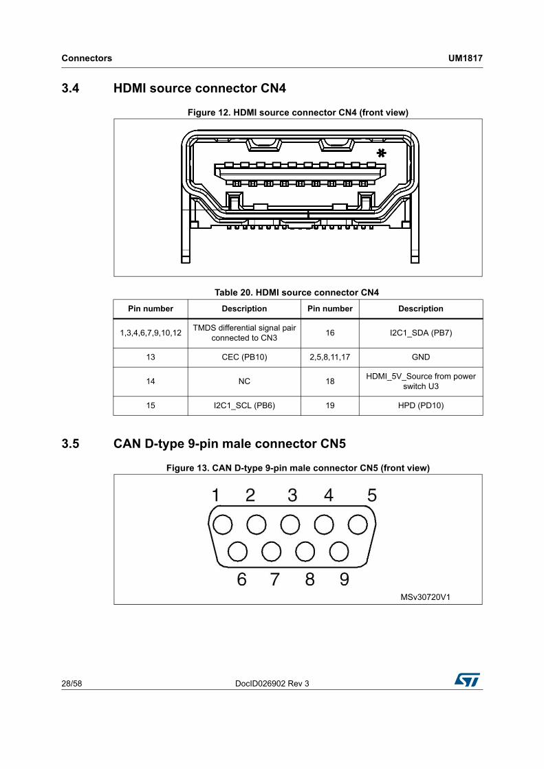
3.4 HDMI source connector CN4
Figure 12. HDMI source connector CN4 (front view)
3.5 CAN D-type 9-pin male connector CN5
Figure 13. CAN D-type 9-pin male connector CN5 (front view)
Table 20. HDMI source connector CN4
Pin number Description Pin number Description
1,3,4,6,7,9,10,12TMDS differential signal pair
connected to CN316 I2C1_SDA (PB7)
13 CEC (PB10) 2,5,8,11,17 GND
14 NC 18HDMI_5V_Source from power
switch U3
15 I2C1_SCL (PB6) 19 HPD (PD10)
DocID026902 Rev 3 29/58
UM1817 Connectors
57
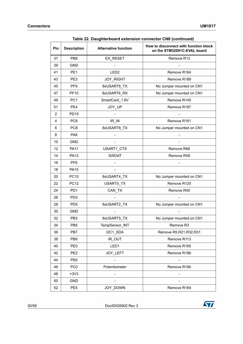
3.6 Daughterboard extension connectors CN6 and CN7
Two 52-pin male headers CN6 and CN7 are used to connect with daughterboard or standard wrapping board to the STM32091C-EVAL evaluation board. All GPIOs are available on it. The space between these two connectors, position of power, GND and RESET pin are defined as a standard which allows developing common daughterboards for several STM32 evaluation boards. The standard width between CN6 pin 1 and CN7 pin 1 is 2700 mils (68.58 mm). Most of evaluation boards implement this standard.
Each pin on CN6 and CN7 can be used by a daughterboard after disconnecting it from the corresponding function block on the STM32091C-EVAL evaluation board. Refer to Table 22 and Table 23 for details.
Table 21. CAN D-type 9-pin male connector CN5
Pin number Description Pin number Description
1,4,8,9 NC 7 CANH
2 CANL 3,5,6 GND
Table 22. Daughterboard extension connector CN6
Pin Description Alternative functionHow to disconnect with function block
on the STM32091C-EVAL board
1 GND - -
3 PC7 - -
5 PC9 8xUSART8_RX No Jumper mounted on CN1
7 PA9 8xUSART1_TX/USART1_TX Remove R52, No Jumper mounted on CN1
9 PA10 8xUSART1_RX/USART1_RX no Jumper mounted on JP1
Pin Description Alternative FunctionHow to disconnect with function block
on STM32091C-EVAL board
DocID026902 Rev 3 33/58
UM1817 Connectors
57
3.8 RS-232 and RS-485 connector CN9
Figure 15. RS-232 and RS-485 connector CN9 (front view)
Table 24. microSD connector CN8
Pin number Description
1 NC
2 SDcard_CS (PE12)
3 SDcard_DIN (PE15)
4 +3V3
5 SDcard_CLK (PE13)
6 Vss/GND
7 SDcard_DOUT (PE14)
8 NC
10 SDcard_detect (PE11)
Table 25. RS-232 and RS-485 connector CN9
Pin number Description
1 NC
2 RS232_RX (PA10)
3 RS232_TX (PA9)
4 RS485_A
5 GND
6 Bootloader_BOOT0
7 RS232_RTS (PA12)
8 RS232_CTS (PA11)/Bootloader_RESET
9 RS485_B
Connectors UM1817
34/58 DocID026902 Rev 3
3.9 High density SWD connector CN10
Figure 16. High density SWD debugging connector CN10 (top view)
Table 26. High density SWD connector CN10
Pin number Description
1 VDDIO2
3 GND
5 GND
7 KEY
9 GND
2 SWDAT (PA13)
4 SWCLK (PA14)
6 NC
8 NC
10 RESET#
DocID026902 Rev 3 35/58
UM1817 Connectors
57
3.10 Standard SWD connector CN11
Figure 17. Standard SWD debugging connector CN11 (top view)
Table 27. Standard SWD debugging connector CN11
Pin number Description
1 VDDIO2
3 NC
5 NC
7 SWDAT (PA13)
9 SWCLK (PA14)
11 10K pull-down
13 NC
15 RESET#
17 10K pull-down
19 10K pull-down
2 VDDIO2
4 GND
6 GND
8 GND
10 GND
12 GND
14 GND
16 GND
18 GND
20 GND
Connectors UM1817
36/58 DocID026902 Rev 3
3.11 ST-LINK/V2-1 USB Type-B connector CN12
The USB connector CN12 is used to connect embedded ST-LINK/V2-1 to PC for debugging of board.
Figure 18. USB Type-B connector CN12 (front view)
3.12 Audio jack CN13
A 3.5 mm stereo audio jack CN13 connected to audio DAC and ADC is available on the STM32091C-EVAL board.
3.13 FT LCD connector CN14
A TFT color LCD board is mounted on CN14. Refer to Section 2.20 for details.
3.14 ST-LINK/V2-1 programming connector CN15
The connector CN15 is used only for embedded ST-LINK/V2-1 programming during board manufacturing. It is not populated by default and not for end user.
3.15 Power connector CN16
The STM32091C-EVAL evaluation board can be powered from a DC 5 V power supply via the external power supply jack (CN16) shown in Figure 16. The central pin of CN16 must be positive.
Table 28. USB Type-B connector CN12
Pin number Description
1 VBUS (power)
2 DM
3 DP
4 GND
5,6 Shield
DocID026902 Rev 3 37/58
UM1817 Connectors
57
Figure 19. Power supply connector CN16 (front view)
STMicroelectronics NV and its subsidiaries (“ST”) reserve the right to make changes, corrections, enhancements, modifications, and improvements to ST products and/or to this document at any time without notice. Purchasers should obtain the latest relevant information on ST products before placing orders. ST products are sold pursuant to ST’s terms and conditions of sale in place at the time of order acknowledgement.
Purchasers are solely responsible for the choice, selection, and use of ST products and ST assumes no liability for application assistance or the design of Purchasers’ products.
No license, express or implied, to any intellectual property right is granted by ST herein.
Resale of ST products with provisions different from the information set forth herein shall void any warranty granted by ST for such product.
ST and the ST logo are trademarks of ST. All other product or service names are the property of their respective owners.
Information in this document supersedes and replaces information previously supplied in any prior versions of this document.