General Description The MAX6870/MAX6871 EEPROM-configurable, multi- voltage supply sequencers/supervisors monitor several voltage detector inputs, two auxiliary inputs, and four general-purpose logic inputs. The MAX6870/MAX6871 feature programmable outputs for highly configurable power-supply sequencing applications. The MAX6870 features six voltage detector inputs and eight program- mable outputs, while the MAX6871 features four voltage detector inputs and five programmable outputs. Manual reset and margin disable inputs offer additional flexibility. All voltage detectors offer two configurable thresholds for undervoltage/overvoltage or dual undervoltage detection. One high voltage input (IN1) provides detec- tor threshold voltages from +2.5V to +13.2V in 50mV increments, or from +1.25V to +7.625V in 25mV incre- ments. A bipolar input (IN2) provides detector threshold voltages from ±2.5V to ±15.25V in 50mV increments, or from ±1.25V to ±7.625V in 25mV increments. Positive inputs (IN3–IN6) provide detector threshold voltages from +1V to +5.5V in 20mV increments, or from +0.5V to +3.05V in 10mV increments. Programmable output stages control power-supply sequencing or system resets/interrupts. Programmable output options include: active-high, active-low, open- drain, weak pullup, push-pull, and charge pump. Programmable timing delay blocks configure each output to wait between 25μs and 1600ms before deasserting. A fault register logs the condition that caused each output to assert (undervoltage, overvoltage, manual reset, etc.). An internal 10-bit ADC monitors the voltage detector inputs, and two auxiliary inputs through a multiplexer that automatically sequences through all inputs every 200ms. A SMBus TM -/I 2 C T -compatible, serial data inter- face programs and communicates with the configuration EEPROM, the configuration registers, the internal 4kb user EEPROM, the ADC registers, and the fault registers of the MAX6870/MAX6871. The MAX6870/MAX6871 are available in a 7mm x 7mm x 0.8mm 32-pin thin QFN package and operate over the extended -40°C to +85°C temperature range. Applications Telecommunications/Central Office Systems Networking Systems Servers/Workstations Basestations Storage Equipment Multimicroprocessor/Voltage Systems Features ♦ Six (MAX6870) or Four (MAX6871) Configurable Input Voltage Detectors One High Voltage Input (+1.25V to +7.625V or +2.5V to +13.2V Thresholds) One Bipolar Voltage Input (±1.25V to ±7.625V or ±2.5V to ±15.25V Thresholds) Four (MAX6870) or Two (MAX6871) Positive Voltage Inputs (+0.5V to +3.05V or +1V to +5.5V Thresholds) ♦ Four General-Purpose Logic Inputs ♦ Two Configurable Watchdog Timers ♦ Eight (MAX6870) or Five (MAX6871) Programmable Outputs Active-High, Active-Low, Open-Drain, Weak Pullup, Push-Pull, Charge-Pump Timing Delays from 25μs to 1600ms ♦ 10-Bit Internal ADC Monitors the Input Voltage Detectors and Two Auxiliary Inputs ♦ Margining Disable and Manual Reset Controls ♦ Internal 1.25V Reference or External Reference Input ♦ 4kb Internal User EEPROM Endurance: 100,000 Erase/Write Cycles Data Retention: 10 Years ♦ I 2 C/SMBus-Compatible Serial Configuration/Communication Interface ♦ ±1% Threshold Accuracy MAX6870/MAX6871 EEPROM-Programmable Hex/Quad Power-Supply Sequencers/Supervisors with ADC ________________________________________________________________ Maxim Integrated Products 1 Ordering Information 19-3384; Rev 1; 9/04 For pricing, delivery, and ordering information, please contact Maxim/Dallas Direct! at 1-888-629-4642, or visit Maxim’s website at www.maxim-ic.com. EVALUATION KIT AVAILABLE Pin Configurations, Typical Operating Circuit, and Selector Guide appear at end of data sheet. PART TEMP RANGE PIN- PACKAGE PKG CODE MAX6870ETJ -40°C to +85°C 32 Thin QFN T3277-2 MAX6871ETJ -40°C to +85°C 32 Thin QFN T3277-2 SMBus is a trademark of Intel Corp.
Transcript
General DescriptionThe MAX6870/MAX6871 EEPROM-configurable, multi-voltage supply sequencers/supervisors monitor severalvoltage detector inputs, two auxiliary inputs, and fourgeneral-purpose logic inputs. The MAX6870/MAX6871feature programmable outputs for highly configurablepower-supply sequencing applications. The MAX6870features six voltage detector inputs and eight program-mable outputs, while the MAX6871 features four voltagedetector inputs and five programmable outputs. Manualreset and margin disable inputs offer additional flexibility.
All voltage detectors offer two configurable thresholdsfor undervoltage/overvoltage or dual undervoltagedetection. One high voltage input (IN1) provides detec-tor threshold voltages from +2.5V to +13.2V in 50mVincrements, or from +1.25V to +7.625V in 25mV incre-ments. A bipolar input (IN2) provides detector thresholdvoltages from ±2.5V to ±15.25V in 50mV increments, orfrom ±1.25V to ±7.625V in 25mV increments. Positiveinputs (IN3–IN6) provide detector threshold voltagesfrom +1V to +5.5V in 20mV increments, or from +0.5Vto +3.05V in 10mV increments.
Programmable output stages control power-supplysequencing or system resets/interrupts. Programmableoutput options include: active-high, active-low, open-drain, weak pullup, push-pull, and charge pump.Programmable timing delay blocks configure each outputto wait between 25µs and 1600ms before deasserting. Afault register logs the condition that caused each outputto assert (undervoltage, overvoltage, manual reset, etc.).
An internal 10-bit ADC monitors the voltage detectorinputs, and two auxiliary inputs through a multiplexerthat automatically sequences through all inputs every200ms. A SMBusTM-/I2CT-compatible, serial data inter-face programs and communicates with the configurationEEPROM, the configuration registers, the internal 4kbuser EEPROM, the ADC registers, and the fault registersof the MAX6870/MAX6871.
The MAX6870/MAX6871 are available in a 7mm x 7mmx 0.8mm 32-pin thin QFN package and operate overthe extended -40°C to +85°C temperature range.
ApplicationsTelecommunications/Central Office SystemsNetworking SystemsServers/WorkstationsBasestationsStorage EquipmentMultimicroprocessor/Voltage Systems
Features♦ Six (MAX6870) or Four (MAX6871) Configurable
Input Voltage DetectorsOne High Voltage Input (+1.25V to +7.625V or
+2.5V to +13.2V Thresholds)One Bipolar Voltage Input (±1.25V to ±7.625V
or ±2.5V to ±15.25V Thresholds)Four (MAX6870) or Two (MAX6871) Positive
Voltage Inputs (+0.5V to +3.05V or +1V to +5.5V Thresholds)
♦ Four General-Purpose Logic Inputs
♦ Two Configurable Watchdog Timers
♦ Eight (MAX6870) or Five (MAX6871)Programmable Outputs
ELECTRICAL CHARACTERISTICS(VIN1 = +6.5V to +13.2V, VIN2 = +10V, VIN3 to VIN6 = +2.7V to +5.5V, AUXIN_ = GPI_ = GND, MARGIN = MR = DBP, TA = -40°C to+85°C, unless otherwise noted. Typical values are at TA = +25°C.) (Notes 1 and 2)
Stresses beyond those listed under “Absolute Maximum Ratings” may cause permanent damage to the device. These are stress ratings only, and functionaloperation of the device at these or any other conditions beyond those indicated in the operational sections of the specifications is not implied. Exposure toabsolute maximum rating conditions for extended periods may affect device reliability.
All Voltages referenced to GNDIN3–IN6, ABP, SDA, SCL, A0, A1,
GPI1–GPI4, MR, MARGIN, PO5–PO8 (MAX6870), PO3/PO4/PO5 (MAX6871)............-0.3V to +6V
IN1, PO1–PO4 (MAX6870), PO1/PO2 (MAX6871)....-0.3V to +14VIN2 ...........................................................................-20V to +20VDBP, AUXIN1, AUXIN2, REFIN.................................-0.3V to +3VInput/Output Current (all pins)..........................................±20mA
Continuous Power Dissipation (TA = +70°C)32-Pin 7mm x 7mm Thin QFN (derate 33.3mW/°C above +70°C).............................2667mW
Operating Temperature Range ...........................-40°C to +85°CMaximum Junction Temperature .....................................+150°CStorage Temperature Range .............................-65°C to +150°CLead Temperature (soldering, 10s) .................................+300°C
PARAMETER SYM B O L CONDITIONS MIN TYP MAX UNITS
VIN1Voltage on IN1 to ensure the device is fullyoperational, IN3 to IN6 = GND
4.0 13.2Operating Voltage Range(Note 3) VIN3 to
VIN6
Voltage on any one of IN3 to IN6 to ensurethe device is fully operational, IN1 = GND
2.7 5.5
V
IN1 Supply Voltage(Note 3)
VIN1PMinimum voltage on IN1 to guarantee that thedevice is powered through IN1
6.5 V
Undervoltage Lockout VUVLOMinimum voltage on one of IN3 to IN6 toguarantee the device is EEPROM configured.
2.5 V
VIN1 = +13.2V, IN2 to IN6 = GND, no load 1.2 1.5
Supply Current ICC Writing to configuration registers or EEPROM,no load
1.3 2mA
VIN1 (50mV increments) 2.5 13.2
VIN1 (25mV increments) 1.250 7.625
VIN2 (50mV increments) ±2.50 ±15.25
VIN2 (25mV increments) ±1.250 ±7.625
VIN3 to VIN6 (20mV increments) 1.0 5.5
Threshold Range VTH
VIN3 to VIN6 (10mV increments) 0.50 3.05
V
TA = +25°C -1.0 +1.0IN1 to IN6 positive,VIN_ falling TA = -40°C to +85°C -1.5 +1.5
TA = +25°C -1.5 +1.5-15.25V ≤ VIN2 ≤ -5V,VIN2 falling TA = -40°C to +85°C -2 +2
%
TA = +25°C -75 +75
Threshold Accuracy
-5V ≤ VIN2 ≤ 0, VIN2falling TA = -40°C to +85°C -100 +100
mV
Threshold Hysteresis VTH-HYST 0.3 % VTH
Reset Threshold TemperatureCoefficient
∆VTH/°C 10ppm/
°C
Threshold-Voltage DifferentialNonlinearity
VTH DNL -1 +1 LSB
MA
X6
87
0/M
AX
68
71
EEPROM-Programmable Hex/QuadPower-Supply Sequencers/Supervisors with ADC
Note 1: Specifications guaranteed for the stated global conditions. The device also meets the parameters specified when 0 < VIN1< +6.5V, and at least one of VIN3 through VIN6 is between +2.7V and +5.5V, while the remaining VIN3 through VIN6 are between 0 and +5.5V.
Note 2: Device may be supplied from any one of IN_, except IN2.Note 3: The internal supply voltage, measured at ABP, equals the maximum of IN3 to IN6 if VIN1 = 0, or equals +5.4V if VIN1 >
+6.5V. For +4V < VIN1 < +6.5V and VIN3 through VIN6 > +2.7V, the input that powers the device cannot be determined.Note 4: 100% production tested at TA = +25°C and TA = +125°C. Specifications at TA = -40°C are guaranteed by design.Note 5: VIN_ > 0.3 x ADC range.Note 6: Does not include the inaccuracy of the external +1.25V voltage reference.Note 7: DNL implicitly guaranteed by design in a sigma-delta converter.Note 8: CBUS = total capacitance of one bus line in pF. Rise and fall times are measured between 0.1 x VBUS and 0.9 x VBUS.Note 9: Input filters on SDA, SCL, A0, and A1 suppress noise spikes < 50ns.Note 10: An additional cycle is required when writing to configuration memory for the first time.
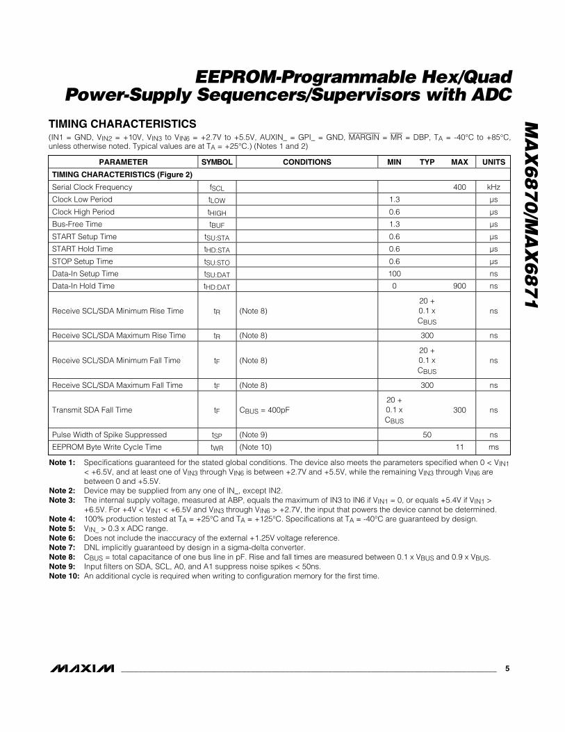
TIMING CHARACTERISTICS(IN1 = GND, VIN2 = +10V, VIN3 to VIN6 = +2.7V to +5.5V, AUXIN_ = GPI_ = GND, MARGIN = MR = DBP, TA = -40°C to +85°C,unless otherwise noted. Typical values are at TA = +25°C.) (Notes 1 and 2)
PARAMETER SYM B O L CONDITIONS MIN TYP MAX UNITS
TIMING CHARACTERISTICS (Figure 2)
Serial Clock Frequency fSCL 400 kHz
Clock Low Period tLOW 1.3 µs
Clock High Period tHIGH 0.6 µs
Bus-Free Time tBUF 1.3 µs
START Setup Time tSU:STA 0.6 µs
START Hold Time tHD:STA 0.6 µs
STOP Setup Time tSU:STO 0.6 µs
Data-In Setup Time tSU:DAT 100 ns
Data-In Hold Time tHD:DAT 0 900 ns
Receive SCL/SDA Minimum Rise Time tR (Note 8)20 +0.1 xCBUS
ns
Receive SCL/SDA Maximum Rise Time tR (Note 8) 300 ns
Receive SCL/SDA Minimum Fall Time tF (Note 8)20 +0.1 xCBUS
ns
Receive SCL/SDA Maximum Fall Time tF (Note 8) 300 ns
Transmit SDA Fall Time tF CBUS = 400pF20 +0.1 xCBUS
300 ns
Pulse Width of Spike Suppressed tSP (Note 9) 50 ns
EEPROM Byte Write Cycle Time tWR (Note 10) 11 ms
MA
X6
87
0/M
AX
68
71
EEPROM-Programmable Hex/QuadPower-Supply Sequencers/Supervisors with ADC
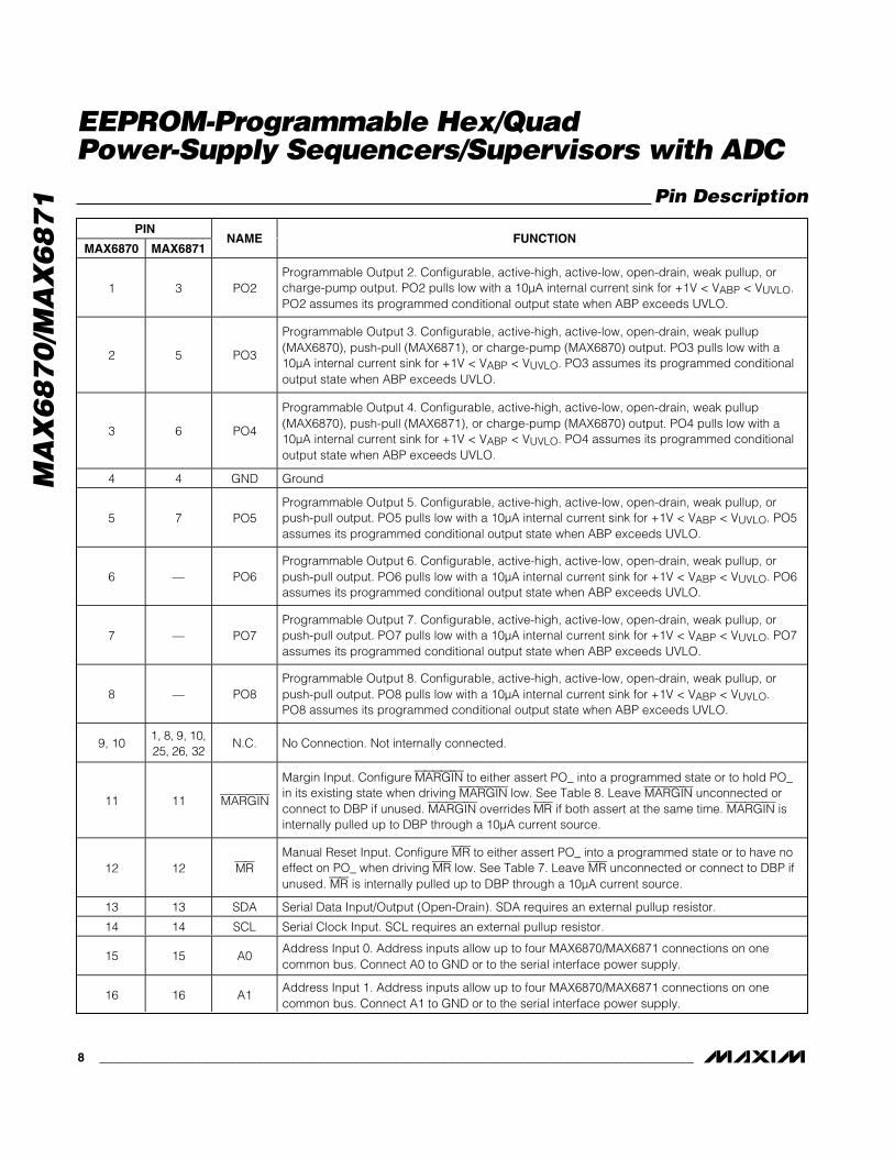
1 3 PO2Programmable Output 2. Configurable, active-high, active-low, open-drain, weak pullup, orcharge-pump output. PO2 pulls low with a 10µA internal current sink for +1V < VABP < VUVLO.PO2 assumes its programmed conditional output state when ABP exceeds UVLO.
2 5 PO3
Programmable Output 3. Configurable, active-high, active-low, open-drain, weak pullup(MAX6870), push-pull (MAX6871), or charge-pump (MAX6870) output. PO3 pulls low with a10µA internal current sink for +1V < VABP < VUVLO. PO3 assumes its programmed conditionaloutput state when ABP exceeds UVLO.
3 6 PO4
Programmable Output 4. Configurable, active-high, active-low, open-drain, weak pullup(MAX6870), push-pull (MAX6871), or charge-pump (MAX6870) output. PO4 pulls low with a10µA internal current sink for +1V < VABP < VUVLO. PO4 assumes its programmed conditionaloutput state when ABP exceeds UVLO.
4 4 GND Ground
5 7 PO5Programmable Output 5. Configurable, active-high, active-low, open-drain, weak pullup, orpush-pull output. PO5 pulls low with a 10µA internal current sink for +1V < VABP < VUVLO. PO5assumes its programmed conditional output state when ABP exceeds UVLO.
6 — PO6Programmable Output 6. Configurable, active-high, active-low, open-drain, weak pullup, orpush-pull output. PO6 pulls low with a 10µA internal current sink for +1V < VABP < VUVLO. PO6assumes its programmed conditional output state when ABP exceeds UVLO.
7 — PO7Programmable Output 7. Configurable, active-high, active-low, open-drain, weak pullup, orpush-pull output. PO7 pulls low with a 10µA internal current sink for +1V < VABP < VUVLO. PO7assumes its programmed conditional output state when ABP exceeds UVLO.
8 — PO8Programmable Output 8. Configurable, active-high, active-low, open-drain, weak pullup, orpush-pull output. PO8 pulls low with a 10µA internal current sink for +1V < VABP < VUVLO.PO8 assumes its programmed conditional output state when ABP exceeds UVLO.
9, 101, 8, 9, 10,25, 26, 32
N.C. No Connection. Not internally connected.
11 11 MARGIN
Margin Input. Configure MARGIN to either assert PO_ into a programmed state or to hold PO_in its existing state when driving MARGIN low. See Table 8. Leave MARGIN unconnected orconnect to DBP if unused. MARGIN overrides MR if both assert at the same time. MARGIN isinternally pulled up to DBP through a 10µA current source.
12 12 MRManual Reset Input. Configure MR to either assert PO_ into a programmed state or to have noeffect on PO_ when driving MR low. See Table 7. Leave MR unconnected or connect to DBP ifunused. MR is internally pulled up to DBP through a 10µA current source.
13 13 SDA Serial Data Input/Output (Open-Drain). SDA requires an external pullup resistor.
14 14 SCL Serial Clock Input. SCL requires an external pullup resistor.
15 15 A0Address Input 0. Address inputs allow up to four MAX6870/MAX6871 connections on onecommon bus. Connect A0 to GND or to the serial interface power supply.
16 16 A1Address Input 1. Address inputs allow up to four MAX6870/MAX6871 connections on onecommon bus. Connect A1 to GND or to the serial interface power supply.
MA
X6
87
0/M
AX
68
71
EEPROM-Programmable Hex/QuadPower-Supply Sequencers/Supervisors with ADC
17 17 GPI4General-Purpose Logic Input 4. An internal 10µA current source pulls GPI4 to GND. ConfigureGPI4 to control watchdog timer functions or the programmable outputs.
18 18 GPI3General-Purpose Logic Input 3. An internal 10µA current source pulls GPI3 to GND. ConfigureGPI3 to control watchdog timer functions or the programmable outputs.
19 19 GPI2General-Purpose Logic Input 2. An internal 10µA current source pulls GPI2 to GND. ConfigureGPI2 to control watchdog timer functions or the programmable outputs.
20 20 GPI1General-Purpose Logic Input 1. An internal 10µA current source pulls GPI1 to GND. ConfigureGPI1 to control watchdog timer functions or the programmable outputs.
21 21 ABP
Internal Power-Supply Output. Bypass ABP to GND with a 1µF ceramic capacitor. ABP powersthe internal circuitry of the MAX6870/MAX6871. ABP supplies the input voltage to the internalcharge pumps when the programmable outputs are configured as charge-pump outputs. Donot use ABP to supply power to external circuitry.
22 22 DBPInternal Digital Power-Supply Output. Bypass DBP to GND with a 1µF ceramic capacitor. DBPsupplies power to the EEPROM memory and the internal logic circuitry. Do not use DBP tosupply power to external circuitry.
23 23 AUXIN2Auxiliary Input 2. A 10-bit ADC monitors the input voltage at AUXIN2. The high-impedanceAUXIN2 input accepts input voltages up to VREFIN. AUXIN2 does not influence EEPROM-configurable power-supply sequencing or reset detection functions.
24 24 AUXIN1Auxiliary Input 1. A 10-bit ADC monitors the input voltage at AUXIN1. The high-impedanceAUXIN1 input accepts input voltages up to VREFIN. AUXIN1 does not influence EEPROM-configurable power-supply sequencing or reset detection functions.
25 — IN6Voltage Input 6. Configure IN6 to detect voltage thresholds between +1V and +5.5V in 20mVincrements, or +0.5V to +3.05V in 10mV increments. For improved noise immunity, bypass IN6to GND with a 0.1µF capacitor installed as close to the device as possible.
26 — IN5Voltage Input 5. Configure IN5 to detect voltage thresholds between +1V and +5.5V in 20mVincrements, or +0.5V to +3.05V in 10mV increments. For improved noise immunity, bypass IN5to GND with a 0.1µF capacitor installed as close to the device as possible.
27 27 IN4Voltage Input 4. Configure IN4 to detect voltage thresholds between +1V and +5.5V in 20mVincrements, or +0.5V to +3.05V in 10mV increments. For improved noise immunity, bypass IN4to GND with a 0.1µF capacitor installed as close to the device as possible.
28 28 IN3Voltage Input 3. Configure IN3 to detect voltage thresholds between +1V and +5.5V in 20mVincrements, or +0.5V to +3.05V in 10mV increments. For improved noise immunity, bypass IN3to GND with a 0.1µF capacitor installed as close to the device as possible.
29 29 IN2
Bipolar Voltage Input 2. Configure IN2 to detect negative voltage thresholds from -2.5V to-15.25V in 50mV increments or -1.25V to -7.625V in 25mV increments. Alternatively, configureIN2 to detect positive voltage thresholds from +2.5V to +15.25V in 50mV increments or +1.25Vto +7.625V in 25mV increments. For improved noise immunity, bypass IN2 to GND with a 0.1µFcapacitor installed as close to the device as possible.
MA
X6
87
0/M
AX
68
71
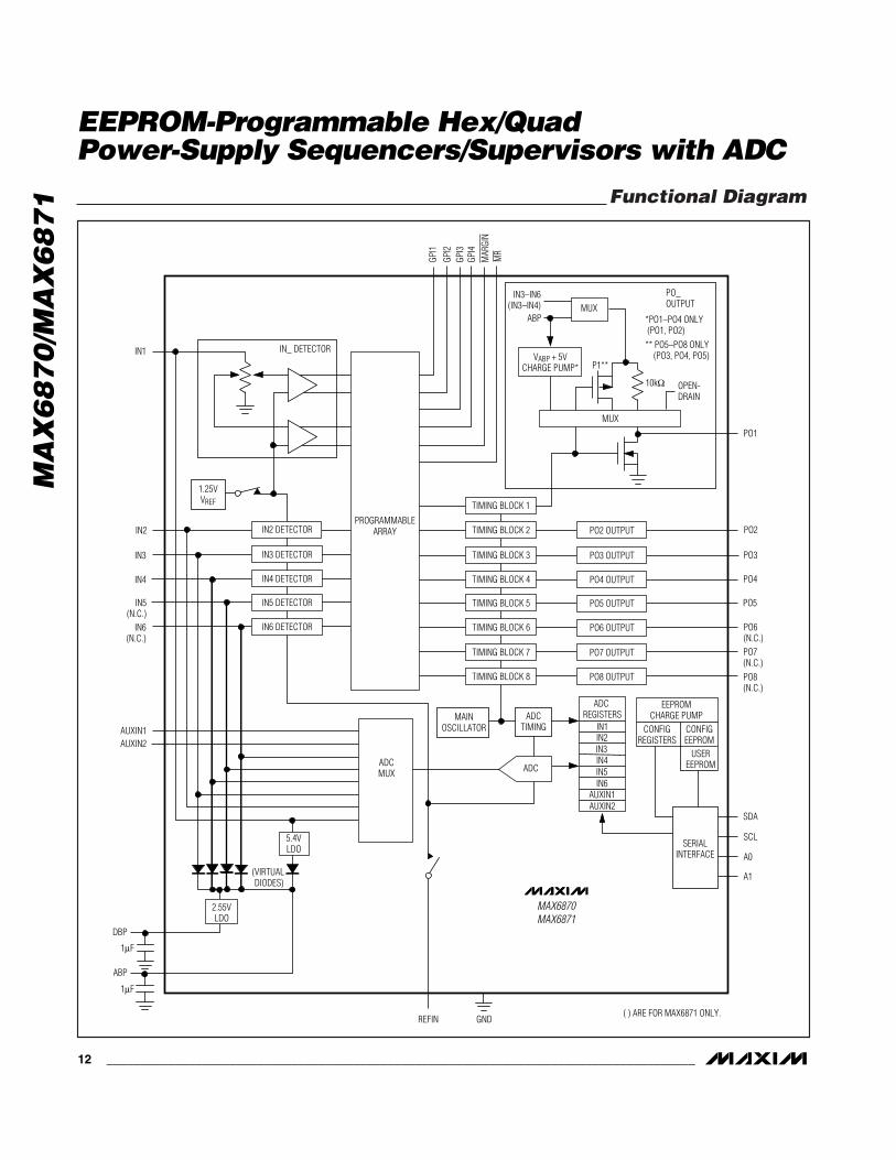
Detailed DescriptionThe MAX6870/MAX6871 EEPROM-configurable, multi-voltage supply sequencers/supervisors monitor severalvoltage-detector inputs, two auxiliary inputs and fourgeneral-purpose logic inputs, and feature programma-ble outputs for highly-configurable, power-supplysequencing applications. The MAX6870 features sixvoltage-detector inputs and eight programmable out-puts, while the MAX6871 features four voltage-detectorinputs and five programmable outputs. Manual resetand margin disable inputs simplify board-level testingduring the manufacturing process. The MAX6870/MAX6871 feature an accurate internal 1.25V reference.For greater accuracy, connect an external +1.25V ref-erence to REFIN.
All voltage detectors provide two configurable thresh-olds for undervoltage/overvoltage or dual undervoltagedetection. One high-voltage input (IN1) provides detec-tor threshold voltages from +1.25V to +7.625V in 25mVincrements or +2.5V to +13.2V in 50mV increments. A bipolar input (IN2) provides detector threshold volt-ages from ±1.25V to ±7.625V in 25mV increments, or±2.5V to ±15.25V in 50mV increments. Positive inputs(IN3–IN6) provide detector threshold voltages from+0.5V to +3.05V in 10mV increments, or +1.0V to +5.5Vin 20mV increments.
An internal 10-bit ADC monitors the voltage-detectorinputs and two auxiliary inputs through a multiplexerthat automatically sequences through all inputs every200ms. The host controller communicates with theMAX6870/MAX6871s’ internal 4kb user EEPROM, configuration EEPROM, configuration registers, ADCregisters, and fault registers through an SMBus/I2C-compatible serial interface (see Figure 1).
Programmable output options include active-high,active-low, open-drain, weak pullup, push-pull, andcharge pump. Select the charge-pump output featureto drive n-channel FETs for power-supply sequencing(see the Applications Information section). The outputsswing between 0 and (VABP + 5V) when configured forcharge-pump operation.
Program each output to assert on any voltage-detectorinput, general-purpose logic input, watchdog timer,manual reset, or other output stages. Programmabletiming-delay blocks configure each output to waitbetween 25µs and 1600ms before deasserting. A faultregister logs the conditions that caused each output toassert (undervoltage, overvoltage, manual reset, etc.).
The MAX6870/MAX6871 feature two watchdog timers,adding flexibility. Program each watchdog timer to assertone or more programmable outputs. Program each
EEPROM-Programmable Hex/QuadPower-Supply Sequencers/Supervisors with ADC
30 30 IN1High Voltage Input 1. Configure IN1 to detect voltage thresholds from +2.5V to +13.2V in 50mVincrements or +1.25V to +7.625V in 25mV increments. For improved noise immunity, bypassIN1 to GND with a 0.1µF capacitor installed as close to the device as possible.
31 31 REFIN
Reference Voltage Input. Configure the MAX6870/MAX6871 to use either an internal referenceor external reference (see Table 9). When configured for an internal reference, leave REFINunconnected. When configured for an external reference, connect a +1.225V to +1.275Vreference to REFIN.
32 2 PO1Programmable Output 1. Configurable active-high, active-low, open-drain, weak pullup, orcharge-pump output. PO1 pulls low with a weak 10µA internal current sink for +1V < VABP< VUVLO. PO1 assumes its programmed conditional output state when ABP exceeds UVLO.
— — EP Exposed Paddle. Exposed paddle is internally connected to GND.
MA
X6
87
0/M
AX
68
71
EEPROM-Programmable Hex/QuadPower-Supply Sequencers/Supervisors with ADC
watchdog timer to clear on a combination of one GPI_input and one programmable output, one of the GPI_inputs only, or one of the programmable outputs only.The initial and normal watchdog timeout periods areindependently programmable from 6.25ms to 102.4s.
A virtual diode-ORing scheme selects the input that pow-ers the MAX6870/MAX6871. The MAX6870/MAX6871
derive power from IN1 if VIN1 > +6.5V or from the highestvoltage on IN3–IN6 if VIN1 < +2.7V. The power sourcecannot be determined if +4V < VIN1 < +6.5V and oneof VIN3 through VIN6 > +2.7V. The programmable out-puts maintain the correct programmed logic state forVABP > VUVLO. One of IN3 through IN6 must begreater than +2.7V or IN1 must be greater than +4V fordevice operation.
MA
X6
87
0/M
AX
68
71
EEPROM-Programmable Hex/QuadPower-Supply Sequencers/Supervisors with ADC
Powering the MAX6870/MAX6871The MAX6870/MAX6871 derive power from the positivevoltage-detector inputs: IN1, or IN3–IN6. A virtual diode-ORing scheme selects the positive input that suppliespower to the device (see the Functional Diagram). IN1must be at least +4V or one of IN3–IN6 (MAX6870)/IN3/IN4 (MAX6871) must be at least +2.7V to ensuredevice operation. An internal LDO regulates IN1 downto +5.4V.
The highest input voltage on IN3–IN6 (MAX6870)/IN3/IN4 (MAX6871) supplies power to the device, unlessVIN1 ≥ +6.5V, in which case IN1 supplies power to thedevice. For +4V < VIN1 < +6.5V and one of VIN3 throughVIN6 > +2.7V, the input power source cannot be deter-mined due to the dropout voltage of the LDO. Internalhysteresis ensures that the supply input that initially pow-ered the device continues to power the device whenmultiple input voltages are within 50mV of each other.
ABP powers the analog circuitry; bypass ABP to GNDwith a 1µF ceramic capacitor installed as close to thedevice as possible. The internal supply voltage, mea-sured at ABP, equals the maximum of IN3– IN6(MAX6870)/IN3/IN4 (MAX6871) if VIN1 = 0, or equals+5.4V when VIN1 > +6.5V. Do not use ABP to providepower to external circuitry.
The MAX6870/MAX6871 also generate a digital supplyvoltage (DBP) for the internal logic circuitry and theEEPROM; bypass DBP to GND with a 1µF ceramiccapacitor installed as close to the device as possible.The nominal DBP output voltage is +2.55V. Do not useDBP to provide power to external circuitry.
ADCThe MAX6870/MAX6871 feature an internal 10-bit ADCthat monitors the voltage-detector inputs and auxiliaryinputs through an internal multiplexer that sequencesthrough all input voltages in 200ms. Registers 50h to5Fh store the ADC data. Read the ADC data from theMAX6870/MAX6871 with the serial interface. The ADCstrictly monitors input voltages and has no effect onpower-supply sequencing, reset detection, or the pro-grammable outputs.
InputsThe MAX6870/MAX6871 contain multiple logic and volt-age-detector inputs. Each voltage-detector input issimultaneously monitored for primary and secondarythresholds. The primary threshold must be an under-voltage threshold. The secondary threshold may be anundervoltage or overvoltage threshold. Table 1 summa-rizes these various inputs.
Table 1. Programmable Features
FEATURE DESCRIPTION
High Voltage Input(IN1)
• Primary undervoltage threshold• Secondary overvoltage or undervoltage threshold• +2.5V to +13.2V threshold in 50mV increments• +1.25V to +7.625V threshold in 25mV increments
Bipolar Voltage Input(IN2)
• Primary undervoltage threshold• Secondary overvoltage or undervoltage threshold• ±2.5V to ±15.25V threshold in 50mV increments• ±1.25V to ±7.625V threshold in 25mV increments
Positive Voltage InputIN3–IN6 (MAX6870)IN3, IN4 (MAX6871)
• Primary undervoltage threshold• Secondary overvoltage or undervoltage threshold• +1V to +5.5V threshold in 20mV increments• +0.5V to +3.05V threshold in 10mV increments
• Active high or active low• Open-drain, weak pullup, or charge-pump output• Weak pullup to IN3–IN6 (IN3 or IN4 for MAX6871) or ABP• Dependent on MR, MARGIN, IN_, GPI1–GPI4 , WDI1 and WDI2, and/or PO_• Programmable timeout periods of 25µs, 1.5625ms, 6.25ms, 25ms, 50ms, 200ms, 400ms, or 1.6s
Programmable OutputsPO5–PO8 (MAX6870),
PO3, PO4, PO5(MAX6871)
• Active high or active low• Open-drain, weak pullup, or push-pull output• Weak pullup to IN3–IN6 (IN3 or IN4 for MAX6871) or ABP• Push-pull to IN3–IN6 (IN3 or IN4 for MAX6871)• Dependent on MR, MARGIN, IN_, GPI1–GPI4 , WDI1 and WDI2 , and/or IN_• Programmable timeout periods of 25µs, 1.5625ms, 6.25ms, 25ms, 50ms, 200ms, 400ms, or 1.6s
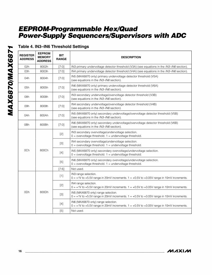
Set the primary and secondary threshold voltages foreach voltage-detector input with registers 00h–0Bh.Each primary threshold voltage must be an undervolt-age threshold. Configure each secondary thresholdvoltage as an undervoltage or overvoltage threshold(see register 0Ch). Set the threshold range for eachvoltage detector with register 0Dh.
High Voltage Input (IN1)IN1 offers threshold voltages of +2.5V to +13.2V in50mV increments, or +1.25V to +7.625V in 25mV incre-ments. Use the following equations to set the thresholdvoltages for IN1:
where VTH is the desired threshold voltage and x is thedecimal code for the desired threshold (Table 2). Forthe +2.5V to +13.2V range, x must equal 214 or less,otherwise the threshold exceeds the maximum operat-ing voltage of IN1.
Bipolar Voltage Input (IN2)IN2 offers negative thresholds from -2.5V to -15.25V in50mV increments, or from -1.25V to -7.625V in 25mVincrements. Alternatively, IN2 offers positive thresholdsfrom +2.5V to +15.25V in 50mV increments, or +1.25Vto +7.625V in 25mV increments. Use the followingequations to set the threshold voltages for IN2:
xV V
Vfor V to V rangeTH= + +
− ..
. . 1 25
0 0251 25 7 625
xV V
Vfor V to V rangeTH= + +
− ..
. . 2 5
0 052 5 13 2
MA
X6
87
0/M
AX
68
71
EEPROM-Programmable Hex/QuadPower-Supply Sequencers/Supervisors with ADC
• Active high or active low logic levels• Configure GPI_ as inputs to watchdog timers or programmable output stages
Watchdog Timers
• Clear dependent on any combination of one GPI_ input and one programmable output, a GPI_ inputonly, or a programmable output only
• Initial watchdog timeout period of 6.25ms, 25ms, 100ms, 400ms, 1.6s, 6.4s, 25.6s, or 102.4s• Normal watchdog timeout period of 6.25ms, 25ms, 100ms, 400ms, 1.6s, 6.4s, 25.6s, or 102.4s• Watchdog enable/disable• Initial watchdog timeout period enable/disable
Auxiliary Inputs(AUXIN1, AUXIN2)
• Monitored by the internal 10-bit ADC
Manual Reset Input(MR)
• Forces PO_ into the active output state when MR = GND• PO_ deassert after MR releases high and the PO_ timeout period expires• PO_ cannot be a function of MR only
Margining Input(MARGIN)
• Holds PO_ in existing state or asserts PO_ to a programmed output state, independent of changes inmonitored inputs or watchdog timers, when MARGIN = GND
• Overrides MR when both assert at the same time
Reference Input(REFIN)
• Internal +1.25V reference voltage• Goes high-impedance when internal reference selected• External reference voltage input from +1.225V to +1.275V• Sets ADC voltage range
10-Bit ADC*
• Monitors IN_, AUXIN1, and AUXIN2• Completes conversion of all eight inputs in 200ms• Reference voltage sets ADC range• Read ADC data from SMBus/I2C interface
Write Disable • Locks user EEPROM based on PO_
Configuration Lock • Locks configuration EEPROM
*ADC does not control programmable outputs.
where VTH is the desired threshold voltage and x is thedecimal code for the desired threshold (Table 3).
IN3–IN6IN3–IN6 offer positive voltage detectors monitor volt-ages from +1V to +5.5V in 20mV increments, or +0.5Vto +3.05V in 10mV increments. Use the following equa-tions to set the threshold voltages for IN_:
where VTH is the desired threshold voltage and x is thedecimal code for the desired threshold (Table 4). Forthe +1V to +5.5V range, x must equal 225 or less, oth-erwise the threshold exceeds the maximum operatingvoltage of IN3–IN6.
xV V
Vfor V to V rangeTH= + +
− ..
. . 0 5
0 010 5 3 05
xV V
Vfor V to V rangeTH= + +
− .
. 1
0 021 5 5
xV V
Vfor V to V rangeTH= + +
− ..
. . 1 25
0 0251 25 7 625
xV V
Vfor V to V rangeTH= + +
− ..
. . 2 5
0 052 5 15 25
xV V
Vfor V to V range
TH=
( )− −
− − .
. . .
1 25
0 0251 25 7 625
xV V
Vfor V to V rangeTH=
( )−
− −−
.
. . .
2 5
0 052 5 15 25
MA
X6
87
0/M
AX
68
71
EEPROM-Programmable Hex/QuadPower-Supply Sequencers/Supervisors with ADC
IN2 range selection.00 = -2.5V to -15.25V range in 50mV increments.01 = -1.25V to -7.625V range in 25mV increments.10 = +2.5V to +15.25V range in 50mV increments.11 = +1.25V to +7.625V range in 25mV increments.
MA
X6
87
0/M
AX
68
71
EEPROM-Programmable Hex/QuadPower-Supply Sequencers/Supervisors with ADC
[1]IN 3 r ang e sel ecti on.0 = + 1V to + 5.5V r ang e i n 20m V i ncr em ents. 1 = + 0.5V to + 3.05V r ang e i n 10m V i ncr em ents.
[2]IN 4 r ang e sel ecti on.0 = + 1V to + 5.5V r ang e i n 20m V i ncr em ents. 1 = + 0.5V to + 3.05V r ang e i n 10m V i ncr em ents.
[3]IN 5 ( M AX 6870 onl y) r ang e sel ecti on.0 = + 1V to + 5.5V r ang e i n 20m V i ncr em ents. 1 = + 0.5V to + 3.05V r ang e i n 10m V i ncr em ents.
[4]IN 6 ( M AX 6870 onl y) r ang e sel ecti on.0 = + 1V to + 5.5V r ang e i n 20m V i ncr em ents. 1 = + 0.5V to + 3.05V r ang e i n 10m V i ncr em ents.
0Dh 800Dh
[5] Not used.
AUXIN1 and AUXIN2The AUXIN1 and AUXIN2 high-impedance analog inputsare intended to monitor two additional system voltagesnot required for power-supply sequencing or reset pur-poses. The internal 10-bit ADC monitors AUXIN1 andAUXIN2 and stores the data in the ADC registers (Table
5). AUXIN1 and AUXIN2 do not assert any of the pro-grammable outputs. The AUXIN1 and AUXIN2 inputsaccept power-supply voltages or other system voltagesscaled to the +1.25V ADC input voltage range.
GPI1–GPI4The GPI1–GPI4 programmable logic inputs controlpower-supply sequencing (programmable outputs),reset/interrupt signaling, and watchdog functions (seethe Configuring the Watchdog Timers (Registers3Ch–3Fh) section). Configure GPI1–GPI4 for active-lowor active-high logic (Table 6). GPI1–GPI4 internally pulldown to GND through a 10µA current sink.
MRThe manual reset (MR) input initiates a reset condition.Register 40h determines the programmable outputs thatassert while MR is low (Table 7). All affected programma-ble outputs remain asserted (see the ProgrammableOutputs section) for their PO_ timeout periods after MRreleases high. An internal 10µA current source pulls MRto DBP. Leave MR unconnected or connect to DBP ifunused. A programmable output cannot depend solelyon MR.
MA
X6
87
0/M
AX
68
71
EEPROM-Programmable Hex/QuadPower-Supply Sequencers/Supervisors with ADC
Table 5. ADC Registers for AUXIN1 andAUXIN2 (Read Only)REGISTERADDRESS
BITRANGE
DESCRIPTION
5Ch [7:0] AUXIN1 measured value, 8 MSBs.
[1:0] AUXIN1 measured value, 2 LSBs.5Dh
[7:2] Not used.
5Eh [7:0] AUXIN2 measured value, 8 MSBs.
[1:0] AUXIN2 measured value, 2 LSBs.5Fh
[7:2] Not used.
Table 6. GPI1–GPI4 Active Logic StatesREGISTERADDRESS
BITRANGE
D ESC R IPT IO N
[0] G P I1. 0 = acti ve l ow . 1 = acti ve hi g h.
[1] G P I2. 0 = acti ve l ow . 1 = acti ve hi g h.
[2] G P I3. 0 = acti ve l ow . 1 = acti ve hi g h.3Bh
[3] G P I4. 0 = acti ve l ow . 1 = acti ve hi g h.
Table 7. Programmable Output Behavior and MR
REGISTERADDRESS
EEPROMMEMORYADDRESS
BITRANGE
DESCRIPTION
[0] PO1 (MAX6870 only). 0 = PO1 independent of MR. 1 = PO1 asserts when MR = low.
[1] PO2 (MAX6870 only). 0 = PO2 independent of MR. 1 = PO2 asserts when MR = low.
[2]PO3 (MAX6870)/PO1 (MAX6871). 0 = PO3/PO1 independent of MR.1 = PO3/PO1 asserts when MR = low.
[3]PO4 (MAX6870)/PO2 (MAX6871). 0 = PO4/PO2 independent of MR.1 = PO4/PO2 asserts when MR = low.
[4]PO5 (MAX6870)/PO3 (MAX6871). 0 = PO5/PO3 independent of MR.1 = PO5/PO3 asserts when MR = low.
[5]PO6 (MAX6870)/PO4 (MAX6871). 0 = PO6/PO4 independent of MR.1 = PO6/PO4 asserts when MR = low.
[6]PO7 (MAX6870)/PO5 (MAX6871). 0 = PO7/PO5 independent of MR.1 = PO7/PO5 asserts when MR = low.
40h 8040h
[7] PO8 (MAX6870 only). 0 = PO8 independent of MR. 1 = PO8 asserts when MR = low.
MA
X6
87
0/M
AX
68
71 MARGIN
MARGIN allows system-level testing while power sup-plies exceed the normal ranges. Registers 41h and 42hdetermine whether the programmable outputs assert toa predetermined state or hold the last state as MARGINis driven low (Table 8). Drive MARGIN low to set theprogrammable outputs in a known state while system-
level testing occurs. Leave MARGIN unconnected orconnect to DBP if unused. An internal 10µA currentsource pulls MARGIN to DBP. The internal ADC contin-ually monitors IN_ while MARGIN is low. The state ofeach programmable output does not change while MARGIN = GND. MARGIN overrides MR if both assert atthe same time.
EEPROM-Programmable Hex/QuadPower-Supply Sequencers/Supervisors with ADC
(MAX6870 only)0 = output held in existing state.1 = output asserts high or low (see 42h[0]).
[1]PO2
(MAX6870 only)0 = output held in existing state.1 = output asserts high or low (see 42h[1]).
[2]PO3 (MAX6870)PO1 (MAX6871)
0 = output held in existing state.1 = output asserts high or low (see 42h[2]).
[3]PO4 (MAX6870)PO2 (MAX6871)
0 = output held in existing state.1 = output asserts high or low (see 42h[3]).
[4]PO5 (MAX6870)PO3 (MAX6871)
0 = output held in existing state.1 = output asserts high or low (see 42h[4]).
[5]PO6 (MAX6870)PO4 (MAX6871)
0 = output held in existing state.1 = output asserts high or low (see 42h[5]).
[6]PO7 (MAX6870)PO5 (MAX6871)
0 = output held in existing state.1 = output asserts high or low (see 42h[6]).
41h 8041h
[7]PO8
(MAX6870 only)0 = output held in existing state.1 = output asserts high or low (see 42h[7]).
[0]PO1
(MAX6870 only)0 = output asserts low if 41h[0] = 1.1 = output asserts high if 41h[0] = 1.
[1]PO2
(MAX6870 only)0 = output asserts low if 41h[1] = 1.1 = output asserts high if 41h[1] = 1.
[2]PO3 (MAX6870)PO1 (MAX6871)
0 = output asserts low if 41h[2] = 1.1 = output asserts high if 41h[2] = 1.
[3]PO4 (MAX6870)PO2 (MAX6871)
0 = output asserts low if 41h[3] = 1.1 = output asserts high if 41h[3] = 1.
[4]PO5 (MAX6870)PO3 (MAX6871)
0 = output asserts low if 41h[4] = 1.1 = output asserts high if 41h[4] = 1.
[5]PO6 (MAX6870)PO4 (MAX6871)
0 = output asserts low if 41h[5] = 1.1 = output asserts high if 41h[5] = 1.
[6]PO7 (MAX6870)PO5 (MAX6871)
0 = output asserts low if 41h[6] = 1.1 = output asserts high if 41h[6] = 1.
42h 8042h
[7]PO8
(MAX6870 only)0 = output asserts low if 41h[7] = 1.1 = output asserts high if 41h[7] = 1.
REFINThe MAX6870/MAX6871 feature an internal +1.25V volt-age reference. The voltage reference sets the thresholdof the voltage detectors and provides a reference volt-age for the internal ADC. Program register 44h to usethe internal reference or an external reference (Table9). Leave REFIN unconnected when using the internalreference. REFIN accepts an external reference in the+1.225V to +1.275V range.
Programmable OutputsThe MAX6870 features eight programmable outputs,while the MAX6871 features five programmable outputs.Selectable output-stage configurations include: active lowor active high, open drain, weak pullup, push-pull, orcharge pump. During power-up, the programmable out-puts pull to GND with an internal 10µA current sink for 1V< VABP < VUVLO. The programmable outputs remain intheir active states until PO_ timeout period expires, andall of the programmed conditions are met for each output.Any output programmed to depend on no conditionalways remains in its active state (Table 22). An active-high configured output is considered asserted when thatoutput is logic-high. No output can depend solely on MR.
The positive voltage monitors generate fault signals(logical 0) to the MAX6870/MAX6871’s logic array whenan input voltage is below the programmed undervolt-age threshold, or when that voltage is above the over-voltage threshold. The negative voltage monitor (IN2)generates a fault signal to the logic array when theinput voltage is less negative than the undervoltagethreshold, or when that voltage is more negative thanthe overvoltage threshold.
Registers 0Eh through 3Ah and 40h configure each ofthe programmable outputs. Programmable timingblocks set the PO_ timeout period from 25µs to 1600msfor each programmable output. See register 3Ah (Table22) to set the active state (active-high or active-low) foreach programmable output and registers 11h, 15h,1Ch, 23h, 2Ah, 31h, 35h, and 39h to select the outputstage types (Tables 23 and 24), and PO_ timeout peri-ods (Table 25) for each output.
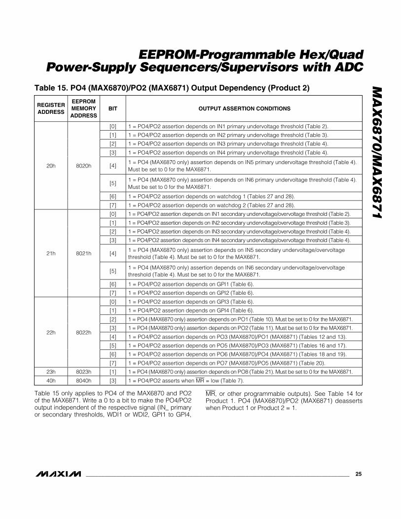
Control selected programmable outputs with a sum ofproducts (Tables 10–21). Each product allows a differ-ent set of conditions to assert each output. OutputsPO3 (MAX6870)/PO1 (MAX6871) and PO6 (MAX6870)/PO4 (MAX6871) allow two sets of different conditions toassert each output. Outputs PO1 and PO2 (MAX6870only), PO7 (MAX6870)/PO5 (MAX6871), and PO8(MAX6870 only) allow only one set of conditions toassert each output.
For example, Product 1 of the PO3 (MAX6870—Table12) programmable output may depend on the IN1 pri-mary undervoltage threshold, and the states of GPI1,PO1, and PO2. Write a one to R16h[0], R17h[6], andR18h[3:2] to configure Product 1 as indicated. IN1must be above the primary undervoltage threshold(Table 2), GPI1 must be inactive (Table 6), and PO1(Tables 10 and 22) and PO2 (Tables 12 and 23) mustbe in their deasserted states for Product 1 to be a logi-cal 1. Product 1 is equivalent to the logic statement:V1A • GPI1 • PO1 • PO2.
Product 2 of PO3 (MAX6870, Table 13) may depend onan entirely different set of conditions, or the same condi-tions, depending on the system requirements. Forexample, Product 2 may depend on the IN1 undervolt-age threshold, and the states of GPI2 and WDI1. Writeones to R19h[6, 0] and R1Ah[7] to configure Product 2as indicated. IN1 must be above the primary undervolt-age threshold (Table 2), GPI2 must be inactive (Table6), and the WDI1 timer must not have expired (Tables27 and 28) for Product 2 to be a logical 1. Product 2 isequivalent to the logic statement: V1A • GPI2 • WDI1.PO3 deasserts if either Product 1 or Product 2 is a logi-cal 1. The logical statement: Product 1 + Product 2determines the state of PO3.
MA
X6
87
0/M
AX
68
71
EEPROM-Programmable Hex/QuadPower-Supply Sequencers/Supervisors with ADC
Table 10 only applies to PO1 of the MAX6870. Write a 0to a bit to make the PO1 output independent of therespective signal (IN1–IN6 primary or secondary
thresholds, WDI1 or WDI2, GPI1–GPI4, MR, or otherprogrammable outputs).
EEPROM-Programmable Hex/QuadPower-Supply Sequencers/Supervisors with ADC
Table 11 only applies to PO2 of the MAX6870. Write a 0to a bit to make the PO2 output independent of therespective signal (IN1–IN6 primary or secondary
thresholds, WDI1 or WDI2, GPI1–GPI4, MR, or otherprogrammable outputs).
MA
X6
87
0/M
AX
68
71
EEPROM-Programmable Hex/QuadPower-Supply Sequencers/Supervisors with ADC
Table 12 only applies to PO3 of the MAX6870 and PO1of the MAX6871. Write a 0 to a bit to make the PO3/PO1output independent of the respective signal (IN_ primaryor secondary thresholds, WDI1 or WDI2, GPI1–GPI4,
MR, or other programmable outputs). See Table 13 forProduct 2. PO3 (MAX6870)/PO1 (MAX6871) deassertswhen Product 1 or Product 2 = 1.
EEPROM-Programmable Hex/QuadPower-Supply Sequencers/Supervisors with ADC
Table 13 only applies to PO3 of the MAX6870 and PO1of the MAX6871. Write a 0 to a bit to make the PO3/PO1output independent of the respective signal (IN_ primaryor secondary thresholds, WDI1 or WDI2, GPI1–GPI4,
MR, or other programmable outputs). See Table 12 forProduct 1. PO3 (MAX6870)/PO1 (MAX6871) deassertswhen Product 1 or Product 2 = 1.
MA
X6
87
0/M
AX
68
71
EEPROM-Programmable Hex/QuadPower-Supply Sequencers/Supervisors with ADC
Table 14 only applies to PO4 of the MAX6870 and PO2of the MAX6871. Write a 0 to a bit to make the PO4/PO2output independent of the respective signal (IN_ primaryor secondary thresholds, WDI1 or WDI2, GPI1–GPI4,
MR, or other programmable outputs). See Table 15 forProduct 2. PO4 (MAX6870)/PO2 (MAX6871) deassertswhen Product 1 or Product 2 = 1.
EEPROM-Programmable Hex/QuadPower-Supply Sequencers/Supervisors with ADC
[4]1 = P O4 ( M AX 6870 onl y) asser ti on d ep end s on IN 5 p r i m ar y und er vol tag e thr eshol d ( Tab l e 4) .M ust b e set to 0 for the M AX 6871.
[5]1 = P O4 ( M AX 6870 onl y) asser ti on d ep end s on IN 6 p r i m ar y und er vol tag e thr eshol d ( Tab l e 4) .M ust b e set to 0 for the M AX 6871.
[6] 1 = PO4/PO2 assertion depends on watchdog 1 (Tables 27 and 28).
1Dh 801Dh
[7] 1 = PO4/PO2 assertion depends on watchdog 2 (Tables 27 and 28).
[0] 1 = P O4/P O2 asser ti on d ep end s on IN 1 second ar y und er vol tag e/over vol tag e thr eshol d ( Tab l e 2) .
[1] 1 = P O4/P O2 asser ti on d ep end s on IN 2 second ar y und er vol tag e/over vol tag e thr eshol d ( Tab l e 3) .
[2] 1 = P O4/P O2 asser ti on d ep end s on IN 3 second ar y und er vol tag e/over vol tag e thr eshol d ( Tab l e 4) .
[3] 1 = P O4/P O2 asser ti on d ep end s on IN 4 second ar y und er vol tag e/over vol tag e thr eshol d ( Tab l e 4) .
[4]1 = PO4 (MAX6870 only) assertion depends on IN5 secondary undervoltage/overvoltagethreshold (Table 4). Must be set to 0 for the MAX6871.
[5]1 = PO4 (MAX6870 only) assertion depends on IN6 secondary undervoltage/overvoltagethreshold (Table 4). Must be set to 0 for the MAX6871.
[6] 1 = PO4/PO2 assertion depends on GPI1 (Table 6).
1Eh 801Eh
[7] 1 = PO4/PO2 assertion depends on GPI2 (Table 6).
[0] 1 = PO4/PO2 assertion depends on GPI3 (Table 6).
[1] 1 = PO4/PO2 assertion depends on GPI4 (Table 6).
[2] 1 = P O4 ( M AX 6870 onl y) asser ti on d ep end s on P O1 ( Tab l e 10) . M ust b e set to 0 for the M AX 6871.
[3] 1 = P O4 ( M AX 6870 onl y) asser ti on d ep end s on P O2 ( Tab l e 11) . M ust b e set to 0 for the M AX 6871.
[4] 1 = P O4/P O 2 asser ti on d ep end s on P O3 ( M AX 6870) /P O 1 ( M AX 6871) ( Tab l es 12 and 13) .
[5] 1 = P O4/P O 2 asser ti on d ep end s on P O5 ( M AX 6870) /P O 3 ( M AX 6871) ( Tab l es 16 and 17) .
[6] 1 = P O4/P O 2 asser ti on d ep end s on P O6 ( M AX 6870) /P O 4 ( M AX 6871) ( Tab l es 18 and 19) .
Table 15 only applies to PO4 of the MAX6870 and PO2of the MAX6871. Write a 0 to a bit to make the PO4/PO2output independent of the respective signal (IN_ primaryor secondary thresholds, WDI1 or WDI2, GPI1 to GPI4,
MR, or other programmable outputs). See Table 14 forProduct 1. PO4 (MAX6870)/PO2 (MAX6871) deassertswhen Product 1 or Product 2 = 1.
MA
X6
87
0/M
AX
68
71
EEPROM-Programmable Hex/QuadPower-Supply Sequencers/Supervisors with ADC
Table 16 only applies to PO5 of the MAX6870 and PO3of the MAX6871. Write a 0 to a bit to make the PO5/PO3output independent of the respective signal (IN_ primaryor secondary thresholds, WDI1 or WDI2, GPI1–GPI4,
MR, or other programmable outputs). See Table 17 forProduct 2. PO5 (MAX6870)/PO3 (MAX6871) deassertswhen Product 1 or Product 2 = 1.
EEPROM-Programmable Hex/QuadPower-Supply Sequencers/Supervisors with ADC
Table 17 only applies to PO5 of the MAX6870 and PO3of the MAX6871. Write a 0 to a bit to make the PO5/PO3output independent of the respective signal (IN_ primaryor secondary thresholds, WDI1 or WDI2, GPI1–GPI4,
MR, or other programmable outputs). See Table 16 forProduct 1. PO5 (MAX6870)/PO3 (MAX6871) deassertswhen Product 1 or Product 2 = 1.
MA
X6
87
0/M
AX
68
71
EEPROM-Programmable Hex/QuadPower-Supply Sequencers/Supervisors with ADC
Table 18 only applies to PO6 of the MAX6870 and PO4of the MAX6871. Write a 0 to a bit to make the PO6/PO4output independent of the respective signal (IN_ primaryor secondary thresholds, WDI1 or WDI2, GPI1–GPI4,
MR, or other programmable outputs). See Table 19 forProduct 2. PO6 (MAX6870)/PO4 (MAX6871) deassertswhen Product 1 or Product 2 = 1.
EEPROM-Programmable Hex/QuadPower-Supply Sequencers/Supervisors with ADC
Table 19 only applies to PO6 of the MAX6870 and PO4of the MAX6871. Write a 0 to a bit to make the PO6/PO4output independent of the respective signal (IN_ primaryor secondary thresholds, WDI1 or WDI2, GPI1–GPI4,
MR, or other programmable outputs). See Table 18 forProduct 1. PO6 (MAX6870)/PO4 (MAX6871) deassertswhen Product 1 or Product 2 = 1.
MA
X6
87
0/M
AX
68
71
EEPROM-Programmable Hex/QuadPower-Supply Sequencers/Supervisors with ADC
Table 20 only applies to PO7 of the MAX6870 and PO5of the MAX6871. Write a 0 to a bit to make the PO7/PO5output independent of the respective signal (IN_ primary
or secondary thresholds, WDI1 or WDI2, GPI1–GPI4,MR, or other programmable outputs).
EEPROM-Programmable Hex/QuadPower-Supply Sequencers/Supervisors with ADC
Table 21 only applies to PO8 of the MAX6870. Write a 0to a bit to make the PO8 output independent of therespective signal (IN1–IN6 primary or secondarythresholds, WDI1 or WDI2, GPI1–GPI4, MR, or otherprogrammable outputs).
Output Stage ConfigurationsIndependently program each programmable output asactive-high or active-low (Table 22). Additionally, pro-gram each programmable output as weak pullup, push-pull, open-drain, or charge pump (Tables 23 and 24).Every programmable output can be configured asopen-drain or weak pullup; however, only PO1–PO4(MAX6870) or PO1/PO2 (MAX6871) can be configured
as charge-pump outputs, and only PO5–PO8(MAX6870) or PO3/PO4/PO5 (MAX6871) can be config-ured as push-pull outputs. Finally, set the PO_ timeoutperiod for each programmable output (Table 25).
An internal 10kΩ resistor provides the pullup resistancefor outputs configured as weak pullup stages. Programeach weak pullup output stage to refer to ABP or one ofthe IN3–IN6 inputs. The programmable outputs source upto 10mA and sink up to 4mA when configured as push-pull stages. Program each push-pull output stage to ref-erence to one of IN3–IN6. PO1–PO4 (MAX6870)/PO1/P02 (MAX6871) pull to VABP + 5V when configuredas charge-pump outputs.
MA
X6
87
0/M
AX
68
71
EEPROM-Programmable Hex/QuadPower-Supply Sequencers/Supervisors with ADC
Charge-Pump Output ConfigurationConfigure the programmable outputs of the MAX6870/MAX6871 as charge-pump outputs to drive n-channelFETs for power-supply sequencing applications. OnlyPO1–PO4 (MAX6870) or PO1 and PO2 (MAX6871) can beconfigured as charge-pump output stages. The charge-pump output high voltage is typically VABP+5.5V when unloaded.
Push-Pull Output ConfigurationThe MAX6870/MAX6871’s programmable outputs sink4mA and source 10mA when configured as push-pulloutputs. Only PO5–PO8 (MAX6870), or PO3/PO4/PO5(MAX6871) can be configured as push-pull outputstages. The push-pull output stages refer to any ofIN3–IN6 (MAX6870)/IN3/IN4 (MAX6871) as configuredin Tables 23 and 24. Use the push-pull output configu-ration to drive loads with fast rise/fall times, or thosewith low impedance.
Weak Pullup Output ConfigurationThe MAX6870/MAX6871’s programmable outputs sink4mA when configured as weak pullups. The weak pullupof 10kΩ refers to any of IN3–IN6 (MAX6870)/IN3/IN4(MAX6871) or ABP as configured in Tables 23 and 24.All programmable outputs of the MAX6870/MAX6871may be configured as weak pullups.
Open-Drain Output ConfigurationConnect an external pullup resistor from the program-mable output to an external voltage when configured asan open-drain output. PO1–PO4 (PO1 and PO2 for theMAX6871) may be pulled up to +13.2V. PO5–PO8(PO3–PO5 for the MAX6871) may be pulled up to avoltage less than or equal to ABP. Choose the pullupresistor depending on the number of devices connect-ed to the open-drain output and the allowable currentconsumption. The open-drain output configuration
allows wire-ORed connections, and provides flexibilityin setting the pullup current.
Configuring the MAX6870/MAX6871The MAX6870/MAX6871 factory-default configurationsets all registers to 00h except 3Ah, which is set to FFh.Each device requires configuration before full power isapplied to the system. To configure the MAX6870/MAX6871, first apply an input voltage to IN1 or one ofIN3–IN6 (MAX6870)/IN3/IN4 (MAX6871) (see thePowering the MAX6870/MAX6871 section). VIN1 > +4Vor one of VIN3–VIN6 > +2.7V, to ensure device operation.Next, transmit data through the serial interface. Use theblock write protocol to quickly configure the device. Writeto the configuration registers first to ensure the device isconfigured properly. After completing the setup proce-dure, use the read word protocol to verify the data fromthe configuration registers. Lastly, use the write wordprotocol to write this data to the EEPROM registers. Aftercompleting EEPROM register configuration, apply fullpower to the system to begin normal operation. The non-volatile EEPROM stores the latest configuration uponremoval of power. Write 0’s to all EEPROM registers toclear the memory.
Software RebootA software reboot allows the user to restore the EEPROM configuration to the volatile registers withoutcycling the power supplies. Use the send byte com-mand with data byte 88h to initiate a software reboot.The 3.5ms (max) power-up delay also applies after asoftware reboot.
SMBus/I2C-Compatible Serial InterfaceThe MAX6870/MAX6871 feature an I2C/SMBus-compati-ble serial interface consisting of a serial data line (SDA)and a serial clock line (SCL). SDA and SCL allow bidirec-tional communication between the MAX6870/MAX6871
and the master device at clock rates up to 400kHz. Figure2 shows the interface timing diagram. TheMAX6870/MAX6871 are transmit/receive slave-onlydevices, relying upon a master device to generate aclock signal. The master device (typically a microcon-troller) initiates data transfer on the bus and generatesSCL to permit that transfer.
A master device communicates to the MAX6870/MAX6871 by transmitting the proper address followed bycommand and/or data words. Each transmit sequence isframed by a START (S) or REPEATED START (SR) condi-tion and a STOP (P) condition. Each word transmittedover the bus is 8 bits long and is always followed by anacknowledge pulse.
SCL is a logic input, while SDA is a logic input/open-drain output. SCL and SDA both require external pullup
resistors to generate the logic-high voltage. Use 4.7kΩfor most applications.
Bit TransferEach clock pulse transfers one data bit. The data onSDA must remain stable while SCL is high (Figure 3),otherwise the MAX6870/MAX6871 register a START orSTOP condition (Figure 4) from the master. SDA andSCL idle high when the bus is not busy.
Start and Stop ConditionsBoth SCL and SDA idle high when the bus is not busy. Amaster device signals the beginning of a transmissionwith a START (S) condition (Figure 4) by transitioningSDA from high to low while SCL is high. The masterdevice issues a STOP (P) condition (Figure 4) by transi-tioning SDA from low to high while SCL is high. A STOP
STOPCONDITION
REPEATED STARTCONDITION
STARTCONDITION
tHIGH
tLOW
tR tF
tSU:DAT tSU:STAtSU:STOtHD:STA
tBUF
tHD:STA
tHD:DAT
SCL
SDA
STARTCONDITION
Figure 2. Serial-Interface Timing Details
DATA LINE STABLE,DATA VALID
SDA
SCL
CHANGE OF DATA ALLOWED
Figure 3. Bit Transfer
PS
STARTCONDITION
SDA
SCL
STOPCONDITION
Figure 4. Start and Stop Conditions
condition frees the bus for another transmission. The busremains active if a REPEATED START condition is gener-ated, such as in the block read protocol (see Figure 7).
Early STOP ConditionsThe MAX6870/MAX6871 recognize a STOP condition atany point during transmission except if a STOP conditionoccurs in the same high pulse as a START condition. Thiscondition is not a legal I2C format. At least one clockpulse must separate any START and STOP condition.
Repeated START ConditionsA REPEATED START (SR) condition may indicate achange of data direction on the bus. Such a changeoccurs when a command word is required to initiate aread operation (see Figure 7). SR may also be usedwhen the bus master is writing to several I2C devicesand does not want to relinquish control of the bus. TheMAX6870/MAX6871 serial interface supports continu-ous write operations with or without an SR conditionseparating them. Continuous read operations requireSR conditions because of the change in direction ofdata flow.
AcknowledgeThe acknowledge bit (ACK) is the 9th bit attached to any8-bit data word. The receiving device always generates
an ACK. The MAX6870/MAX6871 generate an ACKwhen receiving an address or data by pulling SDA lowduring the 9th clock period (Figure 5). When transmittingdata, such as when the master device reads data backfrom the MAX6870/MAX6871, the MAX6870/MAX6871wait for the master device to generate an ACK.Monitoring ACK allows for detection of unsuccessfuldata transfers. An unsuccessful data transfer occurs ifthe receiving device is busy or if a system fault hasoccurred. In the event of an unsuccessful data transfer,the bus master should reattempt communication at alater time. The MAX6870/MAX6871 generate a NACKafter the slave address during a software reboot, whilewriting to the EEPROM, or when receiving an illegalmemory address.
Slave AddressThe MAX6870/MAX6871 slave address conforms to thefollowing table:
MA
X6
87
0/M
AX
68
71
EEPROM-Programmable Hex/QuadPower-Supply Sequencers/Supervisors with ADC
71 SA7 through SA4 represent the standard interface
address (1010) for devices with EEPROM. SA3 and SA2correspond to the A1 and A0 address inputs of theMAX6870/MAX6871 (hard-wired as logic-low or logic-high). SA0 is a read/write flag bit (0 = write, 1 = read).
The A0 and A1 address inputs allow up to fourMAX6870/MAX6871 devices to connect to one bus.Connect A0 and A1 to GND or to the serial interfacepower supply (see Figure 6).
Send ByteThe send byte protocol allows the master device to sendone byte of data to the slave device (see Figure 7). Thesend byte presets a register pointer address for a sub-sequent read or write. The slave sends a NACK insteadof an ACK if the master tries to send an address that isnot allowed. If the master sends 80h, 81h, or 82h, thedata is ACK. This could be start of the write byte/wordprotocol, and the slave expects at least one furtherdata byte. If the master sends a stop condition, theinternal address pointer does not change. If the mastersends 84h, this signifies that the block read protocol isexpected, and a repeated start condition should follow.The device reboots if the master sends 88h. The sendbyte procedure follows:
1) The master sends a start condition.
2) The master sends the 7-bit slave address and awrite bit (low).
3) The addressed slave asserts an ACK on SDA.
4) The master sends an 8-bit data byte.
5) The addressed slave asserts an ACK on SDA.
6) The master sends a stop condition.
Write Byte/WordThe write byte/word protocol allows the master deviceto write a single byte in the register bank, preset anEEPROM (configuration or user) address for a subse-quent read, or to write a single byte to the configurationor user EEPROM (see Figure 7). The write byte/wordprocedure follows:
1) The master sends a start condition.
2) The master sends the 7-bit slave address and awrite bit (low).
3) The addressed slave asserts an ACK on SDA.
4) The master sends an 8-bit command code.
5) The addressed slave asserts an ACK on SDA.
6) The master sends an 8-bit data byte.
7) The addressed slave asserts an ACK on SDA.
8) The master sends a stop condition or sends another8-bit data byte.
9) The addressed slave asserts an ACK on SDA.
10)The master sends a stop condition.
To write a single byte to the register bank, only the 8-bitcommand code and a single 8-bit data byte are sent.The command code must be in the range of 00h to 45h.The data byte is written to the register bank if the com-mand code is valid. The slave generates a NACK atstep 5 if the command code is invalid.
To preset an EEPROM (configuration or user) addressfor a subsequent read, the 8-bit command code and asingle 8-bit data byte are sent. The command codemust be 80h if the write is to be directed into the config-uration EEPROM, or 81h or 82h, if the write is to be
EEPROM-Programmable Hex/QuadPower-Supply Sequencers/Supervisors with ADC
Slave Address–equivalent to chip-select line of a 3-wire interface.
Slave Address–equivalent to chip-select line of a 3-wire interface.
S ADDRESS WR ACK COMMAND ACK DATA ACK P
7 bits 8 bits 8 bits
Slave Address–equivalent to chip-select line of a 3-wire interface.
Command Byte–selects registerbeing written.
Data Byte–data goes into theregister set by the commandbyte if the command is below50h. If the command is 80h,81h, or 82h, the data bytepresets the LSB of an EEPROMaddress.
1 0
0
0 0
10
Figure 7. SMBus/I2C Protocols
MA
X6
87
0/M
AX
68
71 directed into the user EEPROM. If the command code is
80h, the data byte must be in the range of 00h to 45h. Ifthe command code is 81h or 82h, the data byte can be00h to FFh. A NACK is generated in step 7 if none of theabove conditions are true.
To write a single byte of data to the user or configurationEEPROM, the 8-bit command code and a single 8-bitdata byte are sent. The following 8-bit data byte is writ-ten to the addressed EEPROM location.
Block WriteThe block write protocol allows the master device towrite a block of data (1 to 16 bytes) to the EEPROM orto the register bank (see Figure 7). The destinationaddress must already be set by the send byte or writebyte protocol and the command code must be 83h. Ifthe number of bytes to be written causes the addresspointer to exceed 45h for the configuration register orconfiguration EEPROM, the address pointer stays at45h, overwriting this memory address with the remain-ing bytes of data. The last data byte sent is stored atregister address 45h. If the number of bytes to be writ-ten exceeds the address pointer FFh for the user EEP-ROM, the address pointer loops back to 00h, andcontinues writing bytes until all data is written. Theblock write procedure follows:
1) The master sends a start condition.
2) The master sends the 7-bit slave address and awrite bit (low).
3) The addressed slave asserts an ACK on SDA.
4) The master sends the 8-bit command code forblock write (83h).
5) The addressed slave asserts an ACK on SDA.
6) The master sends the 8-bit byte count (1 to 16 bytes) N.
7) The addressed slave asserts an ACK on SDA.
8) The master sends 8-bits of data.
9) The addressed slave asserts an ACK on SDA.
10) Repeat steps 8 and 9 one time.
11) The master generates a stop condition.
Receive ByteThe receive byte protocol allows the master device toread the register content of the MAX6870/MAX6871(see Figure 7). The EEPROM or register address mustbe preset with a send byte or write word protocol first.Once the read is complete, the internal pointer increas-es by one. Repeating the receive byte protocol reads
the contents of the next address. The receive byte pro-cedure follows:
1) The master sends a start condition.
2) The master sends the 7-bit slave address and aread bit (high).
3) The addressed slave asserts an ACK on SDA.
4) The slave sends 8 data bits.
5) The master asserts a NACK on SDA.
6) The master generates a stop condition.
Block ReadThe block read protocol allows the master device toread a block of 16 bytes from the EEPROM or registerbank (see Figure 7). Read fewer than 16 bytes of databy issuing an early STOP condition from the master, orby generating a NACK with the master. The send byteor write byte protocol predetermines the destinationaddress with a command code of 84h. The block readprocedure follows:
1) The master sends a start condition.
2) The master sends the 7-bit slave address and awrite bit (low).
3) The addressed slave asserts an ACK on SDA.
4) The master sends 8 bits of the block read command(84h).
5) The slave asserts an ACK on SDA, unless busy.
6) The master generates a repeated start condition.
7) The master sends the 7-bit slave address and aread bit (high).
8) The slave asserts an ACK on SDA.
9) The slave sends the 8-bit byte count (16).
10)The master asserts an ACK on SDA.
11)The slave sends 8 bits of data.
12)The master asserts an ACK on SDA.
13)Repeat steps 8 and 9 fifteen times.
14)The master generates a stop condition.
Address PointersUse the send byte protocol to set the register addresspointers before read and write operations. For the con-figuration registers, valid address pointers range from00h to 45h. Register addresses outside of this rangeresult in a NACK being issued from the MAX6870/MAX6871. When using the block write protocol, the
EEPROM-Programmable Hex/QuadPower-Supply Sequencers/Supervisors with ADC
address pointer automatically increments after eachdata byte, except when the address pointer is alreadyat 45h. If the address pointer is already 45h, and moredata bytes are being sent, these subsequent bytesoverwrite address 45h repeatedly, leaving only the lastdata byte sent stored at this register address.
For the configuration EEPROM, valid address pointersrange from 8000h to 8045h. Registers 8046h to 804Fhare reserved and should not be overwritten. Registeraddresses from 8050h to 80FFh return a NACK fromthe MAX6870/MAX6871. When using the block writeprotocol, the address pointer automatically incrementsafter each data byte, except when the address pointeris already at 8045h. If the address pointer is already8045h, and more data bytes are being sent, these sub-sequent bytes overwrite address 8045h repeatedly,leaving only the last data byte sent stored at this regis-ter address.
For the user EEPROM, valid address pointers rangefrom 8100h to 81FFh and 8200h to 82FFh. Block writeand block read protocols allow the address pointer toreset (to 8100h or 8200h) when attempting to write orread beyond 81FFh or 82FFh.
Configuration EEPROMThe configuration EEPROM addresses range from 8000hto 8045h. Write data to the configuration EEPROM toautomatically set up the MAX6870/MAX6871 upon power-up. Data transfers from the configuration EEPROM to theconfiguration registers when ABP exceeds UVLO duringpower-up or after a software reboot. After ABP exceedsUVLO, an internal 1MHz clock starts after a 5µs delay,and data transfer begins. Data transfer disables access
to the configuration registers and EEPROM. The datatransfer from EEPROM to configuration registers takes3.5ms (max). Read configuration EEPROM data at anytime after power-up or software reboot. Write commandsto the configuration EEPROM are allowed at any timeafter power-up or software reboot, unless the configura-tion lock bit is set (see Table 30). The maximum cycletime to write a single byte is 11ms (max).
User EEPROMThe 512 byte user EEPROM addresses range from8100h to 82FFh (see Figure 8). Store software-revisiondata, board-revision data, and other data in these reg-isters. The maximum cycle time to write a single byte is11ms (max).
Configuration Register Bank and EEPROMThe configuration registers can be directly modified bythe serial interface without modifying the EEPROM afterthe power-up procedure terminates and the configura-tion EEPROM data has been loaded into the configura-tion register bank. Use the write byte or block writeprotocols to write directly to the configuration registers.Changes to the configuration registers take effectimmediately and are lost upon power removal.
At device power-up, the register bank loads configura-tion data from the EEPROM. Configuration data may bedirectly altered in the register bank during applicationdevelopment, allowing maximum flexibility. Transfer thenew configuration data, byte by byte, to the configura-tion EEPROM with the write byte protocol. The nextdevice power-up or software reboot automatically loadsthe new configuration.
MA
X6
87
0/M
AX
68
71
EEPROM-Programmable Hex/QuadPower-Supply Sequencers/Supervisors with ADC
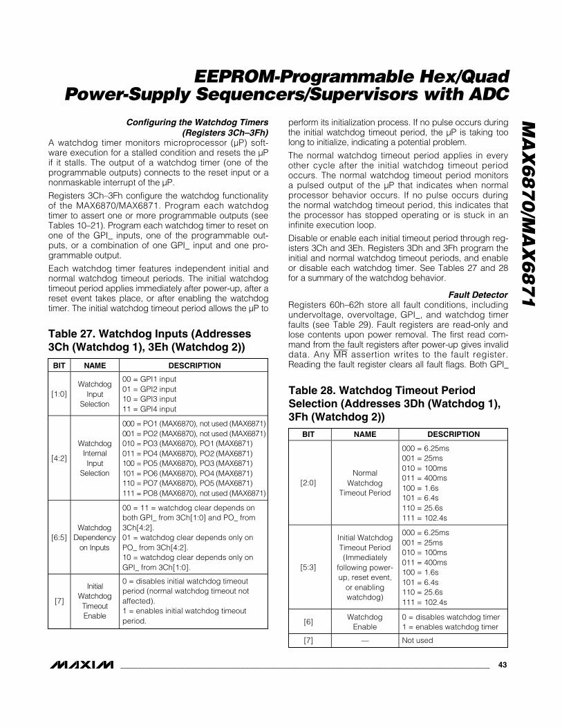
Configuring the Watchdog Timers(Registers 3Ch–3Fh)
A watchdog timer monitors microprocessor (µP) soft-ware execution for a stalled condition and resets the µPif it stalls. The output of a watchdog timer (one of theprogrammable outputs) connects to the reset input or anonmaskable interrupt of the µP.
Registers 3Ch–3Fh configure the watchdog functionalityof the MAX6870/MAX6871. Program each watchdogtimer to assert one or more programmable outputs (seeTables 10–21). Program each watchdog timer to reset onone of the GPI_ inputs, one of the programmable out-puts, or a combination of one GPI_ input and one pro-grammable output.
Each watchdog timer features independent initial andnormal watchdog timeout periods. The initial watchdogtimeout period applies immediately after power-up, after areset event takes place, or after enabling the watchdogtimer. The initial watchdog timeout period allows the µP to
perform its initialization process. If no pulse occurs duringthe initial watchdog timeout period, the µP is taking toolong to initialize, indicating a potential problem.
The normal watchdog timeout period applies in everyother cycle after the initial watchdog timeout periodoccurs. The normal watchdog timeout period monitorsa pulsed output of the µP that indicates when normalprocessor behavior occurs. If no pulse occurs duringthe normal watchdog timeout period, this indicates thatthe processor has stopped operating or is stuck in aninfinite execution loop.
Disable or enable each initial timeout period through reg-isters 3Ch and 3Eh. Registers 3Dh and 3Fh program theinitial and normal watchdog timeout periods, and enableor disable each watchdog timer. See Tables 27 and 28for a summary of the watchdog behavior.
Fault DetectorRegisters 60h–62h store all fault conditions, includingundervoltage, overvoltage, GPI_, and watchdog timerfaults (see Table 29). Fault registers are read-only andlose contents upon power removal. The first read com-mand from the fault registers after power-up gives invaliddata. Any MR assertion writes to the fault register.Reading the fault register clears all fault flags. Both GPI_
000 = P O1 ( M AX 6870) , not used ( M AX 6871) 001 = P O2 ( M AX 6870) , not used ( M AX 6871) 010 = P O3 ( M AX 6870) , P O1 ( M AX 6871) 011 = P O4 ( M AX 6870) , P O2 ( M AX 6871) 100 = P O5 ( M AX 6870) , P O3 ( M AX 6871) 101 = P O6 ( M AX 6870) , P O4 ( M AX 6871) 110 = P O7 ( M AX 6870) , P O5 ( M AX 6871) 111 = P O8 ( M AX 6870) , not used ( M AX 6871)
[6:5]Watchd og
D ep end encyon Inp uts
00 = 11 = watchdog clear depends onboth GPI_ from 3Ch[1:0] and PO_ from3Ch[4:2].01 = watchdog clear depends only onPO_ from 3Ch[4:2].10 = watchdog clear depends only onGPI_ from 3Ch[1:0].
and WDI_ bits assert if any of the GPI_ inputs are config-ured as watchdog inputs (WDI_) and a watchdog faultoccurs.
Configuration LockLock the configuration register bank and configurationEEPROM contents after initial programming by settingthe lock bit high (see Table 30). Locking the configura-tion prevents write operations to all registers except theconfiguration lock register. Clear the lock bit to recon-figure the device.
Write DisableA unique write disable feature protects the MAX6870/MAX6871 from inadvertent user EEPROM writes. Asinput voltages that power the serial interface, a µP, or anyother writing devices fall, unintentional data may be writ-ten onto the data bus. The user EEPROM write disablefunction (see Table 31) ensures that unintentional datadoes not corrupt the MAX6870/MAX6871 EEPROM data.
EEPROM-Programmable Hex/QuadPower-Supply Sequencers/Supervisors with ADC
[0]1 = IN1 falls below secondary undervoltage threshold or rises above secondary overvoltage threshold,depending on the settings in register 0Ch (see Tables 2, 3, and 4).
[1]1 = IN2 falls below secondary undervoltage threshold or rises above secondary overvoltage threshold,depending on the settings in register 0Ch (see Tables 2, 3, and 4).
[2]1 = IN3 falls below secondary undervoltage threshold or rises above secondary overvoltage threshold,depending on the settings in register 0Ch (see Tables 2, 3, and 4).
[3]1 = IN4 falls below secondary undervoltage threshold or rises above secondary overvoltage threshold,depending on the settings in register 0Ch (see Tables 2, 3, and 4).
[4]1 = IN5 (MAX6870 only) falls below secondary undervoltage threshold or rises above secondaryovervoltage threshold, depending on the settings in register 0Ch (see Tables 2, 3, and 4).
[5]1 = IN6 (MAX6870 only) falls below secondary undervoltage threshold or rises above secondaryovervoltage threshold, depending on the settings in register 0Ch (see Tables 2, 3, and 4).
61h
[7:6] Not used.
[0] 1 = WDI1 asserted.
[1] 1 = WDI2 asserted.
[2] 1 = GPI1 asserted.
[3] 1 = GPI2 asserted.
[4] 1 = GPI3 asserted.
[5] 1 = GPI4 asserted.
[6] 1 = MR asserted.
62h
[7] Not used.
Applications InformationConfiguration Download at Power-up
The configuration of the MAX6870/MAX6871 (undervolt-age/overvoltage thresholds, PO_ timeout periods,watchdog behavior, programmable output conditionsand configurations, etc.) depends on the contents ofthe EEPROM. The EEPROM is comprised of bufferedlatches that store the configuration. The local volatilememory latches lose their contents at power-down.Therefore, at power-up, the device configuration mustbe restored by downloading the contents of the EEP-ROM (non-volatile memory) to the local latches. Thisdownload occurs in a number of steps:
1) Programmable outputs go high impedance with nopower applied to the device.
2) When ABP exceeds +1V, all programmable out-puts are weakly pulled to GND through a 10µAcurrent sink.
3) When ABP exceeds UVLO, the configuration EEP-ROM starts to download its contents to the volatileconfiguration registers. The programmable outputsassume their programmed conditional output statewhen download is complete.
4) Any attempt to communicate with the device prior tothis download completion results in a NACK beingissued from the MAX6870/MAX6871.
MA
X6
87
0/M
AX
68
71
EEPROM-Programmable Hex/QuadPower-Supply Sequencers/Supervisors with ADC
[0]0 = write not disabled if PO1 asserts (MAX6870).1 = write disabled if PO1 asserts (MAX6870). Set to 0 (MAX6871).
[1]0 = write not disabled if PO2 asserts (MAX6870).1 = write disabled if PO2 asserts (MAX6870). Set to 0 (MAX6871).
[2]0 = write not disabled if PO3 (MAX6870)/PO1 (MAX6871) asserts.1 = write disabled if PO3 (MAX6870)/PO1 (MAX6871) asserts.
[3]0 = write not disabled if PO4 (MAX6870)/PO2 (MAX6871) asserts.1 = write disabled if PO4 (MAX6870)/PO2 (MAX6871) asserts.
[4]0 = write not disabled if PO5 (MAX6870)/PO3 (MAX6871) asserts.1 = write disabled if PO5 (MAX6870)/PO3 (MAX6871) asserts.
[5]0 = write not disabled if PO6 (MAX6870)/PO4 (MAX6871) asserts.1 = write disabled if PO6 (MAX6870)/PO4 (MAX6871) asserts.
[6]0 = write not disabled if PO7 (MAX6870)/PO5 (MAX6871) asserts.1 = write disabled if PO7 (MAX6870)/PO5 (MAX6871) asserts.
43h 8043h
[7]0 = write not disabled if PO8 asserts (MAX6870).1 = write disabled if PO8 asserts (MAX6870). Set to 0 (MAX6871).
MA
X6
87
0/M
AX
68
71 Forcing Programmable
Outputs High During Power-UpA weak 10µA pulldown holds all programmable outputslow during power-up until ABP exceeds the undervolt-age lockout (UVLO) threshold. Applications requiring aguaranteed high programmable output for ABP down toGND require external pullup resistors to maintain thelogic state until ABP exceeds UVLO. Use 20kΩ resis-tors for most applications.
Driving High-Side MOSFETSwitches with the MAX6870/MAX6871
High-side MOSFET switches are commonly used inpower-supply sequencing applications. First, configurethe programmable output of the MAX6870/MAX6871 asan active-low charge-pump output and set the condi-tions to assert this output. Connect the programmableoutput to the gate of an n-channel MOSFET. As theconditions to deassert this output are met, the outputdeasserts high (VABP +5V), turning on the FET, thusallowing the voltage on the drain to pass through to thedownstream device (see Figure 9).
Uses for General-Purpose Inputs (GPI1–GPI4)
Watchdog TimerProgram GPI_ as an input to one of the watchdogtimers in the MAX6870/MAX6871. The GPI_ input musttoggle within the watchdog timeout period, otherwiseany programmable output dependent on the watchdogtimer asserts.
Additional Manual Reset FunctionsThe PO7 (MAX6870)/PO5 (MAX6871) programmableoutputs allow a single set (Product 1 only) of conditionsto assert the output. Program the set of conditions todepend on one of the GPI_ inputs. Any output thatdepends on GPI_ asserts when GPI_ is held in itsactive state, effectively acting as a manual reset input.
Other Fault Signals from µCConnect a general purpose output from a µC to one ofthe GPI_ inputs to allow interrupts to assert any outputof the MAX6870/MAX6871. Configure one of the pro-grammable outputs to assert on whichever GPI_ inputconnects to the general purpose output of the µC.
Uses for AUXIN1 and AUXIN2Analog Output of Current-Sense Amplifier
Figure 10 shows the MAX6870/MAX6871 in a current-sensing application with the MAX4374. The MAX4374generates an analog output voltage (OUT) proportionalto the voltage difference between RS+ and RS- and alatched comparator output (COUT) indicating an over-current condition. Connect OUT to AUXIN1 to providecontinuous monitoring of the load current on the 12Vsupply. The internal ADC of the MAX6870/MAX6871digitizes VOUT and stores the results in read-only regis-ters 5Ch through 5Fh. COUT latches high for VCIN >600mV, and clears with the RESET input of the MAX4374.Configure GPI1 as an active-high input and configurePO7 (MAX6870)/PO5 (MAX6871) to depend on GPI1.PO7/PO5 asserts to its active state when an overcurrentcondition exists.
EEPROM-Programmable Hex/QuadPower-Supply Sequencers/Supervisors with ADC
Temperature Sensor OutputsFigure 11 shows the MAX6870/MAX6871 in a tempera-ture-sensing application with the DS600. The DS600generates an analog output voltage proportional to thesensed temperature through VOUT and logic outputs onTO and TO (only TO is shown). The internal ADC of theMAX6870/MAX6871 digitizes the analog output voltageof the DS600 and stores the results in read-only regis-ters 5Ch through 5Fh. VTH sets the threshold voltagethat VOUT must exceed for TO to generate a logic-highsignal. VTH must be less than 1.25V, otherwise theovercurrent condition will occur after the internal ADCattains its full-scale input voltage. Configure GPI1 as anactive-high input and configure PO7 (MAX6870)/PO5(MAX6871) to depend on GPI1. When VOUT increasesabove VTH, TO asserts high, causing PO7/PO5 toassert to its active state.
Monitoring Other VoltagesUse AUXIN_ to monitor any voltage up to 1.25V. Theinternal ADC of the MAX6870/MAX6871 digitizes the volt-age and stores the results in read-only registers 5Chthrough 5Fh. The internal ADC cycles through the volt-age monitor inputs and the auxiliary inputs every 200ms.
Layout and BypassingFor better noise immunity, bypass each of the voltagedetector inputs to GND with 0.1µF capacitors installedas close to the device as possible. Bypass ABP andDBP to GND with 1µF capacitors installed as close tothe device as possible. ABP and DBP are internallygenerated voltages and should not be used to supplypower to external circuitry.
Configuration Latency PeriodA delay of less than 5µs occurs between writing to theconfiguration registers and the time when thesechanges actually take place, except when changingone of the voltage-detector thresholds. Changing avoltage-detector threshold typically takes 150µs. Whenchanging EEPROM contents, a software reboot orcycling of power is required for these changes to trans-fer to volatile memory.
Chip InformationPROCESS: BiCMOS
MA
X6
87
0/M
AX
68
71
EEPROM-Programmable Hex/QuadPower-Supply Sequencers/Supervisors with ADC
Package Information(The package drawing(s) in this data sheet may not reflect the most current specifications. For the latest package outline information,go to www.maxim-ic.com/packages.)
EEPROM-Programmable Hex/QuadPower-Supply Sequencers/Supervisors with ADC
Maxim cannot assume responsibility for use of any circuitry other than circuitry entirely embodied in a Maxim product. No circuit patent licenses areimplied. Maxim reserves the right to change the circuitry and specifications without notice at any time.
Maxim Integrated Products, 120 San Gabriel Drive, Sunnyvale, CA 94086 408-737-7600 ____________________ 51
Package Information (continued)(The package drawing(s) in this data sheet may not reflect the most current specifications. For the latest package outline information,go to www.maxim-ic.com/packages.)