ECE1371 Advanced Analog Circuits Lecture 2 EXAMPLE DESIGN– PART 1 Richard Schreier [email protected]Trevor Caldwell [email protected]ECE1371 2-2 Course Goals • Deepen understanding of CMOS analog circuit design through a top-down study of a modern analog system The lectures will focus on Delta-Sigma ADCs, but you may do your project on another analog system. • Develop circuit insight through brief peeks at some nifty little circuits The circuit world is filled with many little gems that every competent designer ought to recognize.
Review: Simulated MOD2 PSDInput at 50% of FullScale
10–3 10–2 10–1–140
–120
–100
–80
–60
–40
–20
0
SQNR = 86 dB@ OSR = 128
40 dB/decade
Theoretical PSD(k = 1)
Simulated spectrum
Normalized Frequency (f /fs )
dB
FS
/NB
W
(smoothed)
NBW = 5.7×10⁻⁷
ECE1371 2-10
Review: Advantages of ∆Σ• ADC: Simplified Anti-Alias Filter
Since the input is oversampled, only very highfrequencies alias to the passband. These can oftenbe removed with a simple RC section.If a continuous-time loop filter is used, the anti-aliasfilter can often be eliminated altogether.
• DAC: Simplified Reconstruction FilterThe nearby images present in Nyquist-ratereconstruction can be removed digitally.
+ Inherent LinearitySimple structures can yield very high SNR.
Signal Swing• So far, we have not paid any attention to how
much swing the op amps can support, or to themagnitudes of u, Vref, x1 and x2
• For simplicity, assume:the full-scale range of u is ±1 V,the op-amp swing is also ±1 V andVref = 1 V
• We still need to know the ranges of x1 and x2 inorder to accomplish dynamic-range scaling
ECE1371 2-27
Dynamic-Range Scaling• In a linear system with known state bounds, the
states can be scaled to occupy any desiredrange
z 1– xα2
α1
z 1–
β2
β1
x k⁄ k β2
kβ1
α2 k⁄
α1 k⁄
e.g. one state oforiginal system:
state scaledby 1/k:
ECE1371 2-28
State Swings in MOD2Linear Theory
• If u is constant and e is white with power, then , ,
and
Q1z−1
zz−1
U VE
X1 X2
V z 1– U 1 z 1––( )2E+=
X 1z
z 1–------------ U V–( ) U 1 z 1––( )E–= =
X 2 V E– z 1– U 2– z 1– z 2–+( )E+= =
σe2 1 3⁄= x 1 u= σx 1
2 2σe2 2 3⁄= =
x 2 u= σx 22 5σe
2 5 3⁄= =
ECE1371 2-29
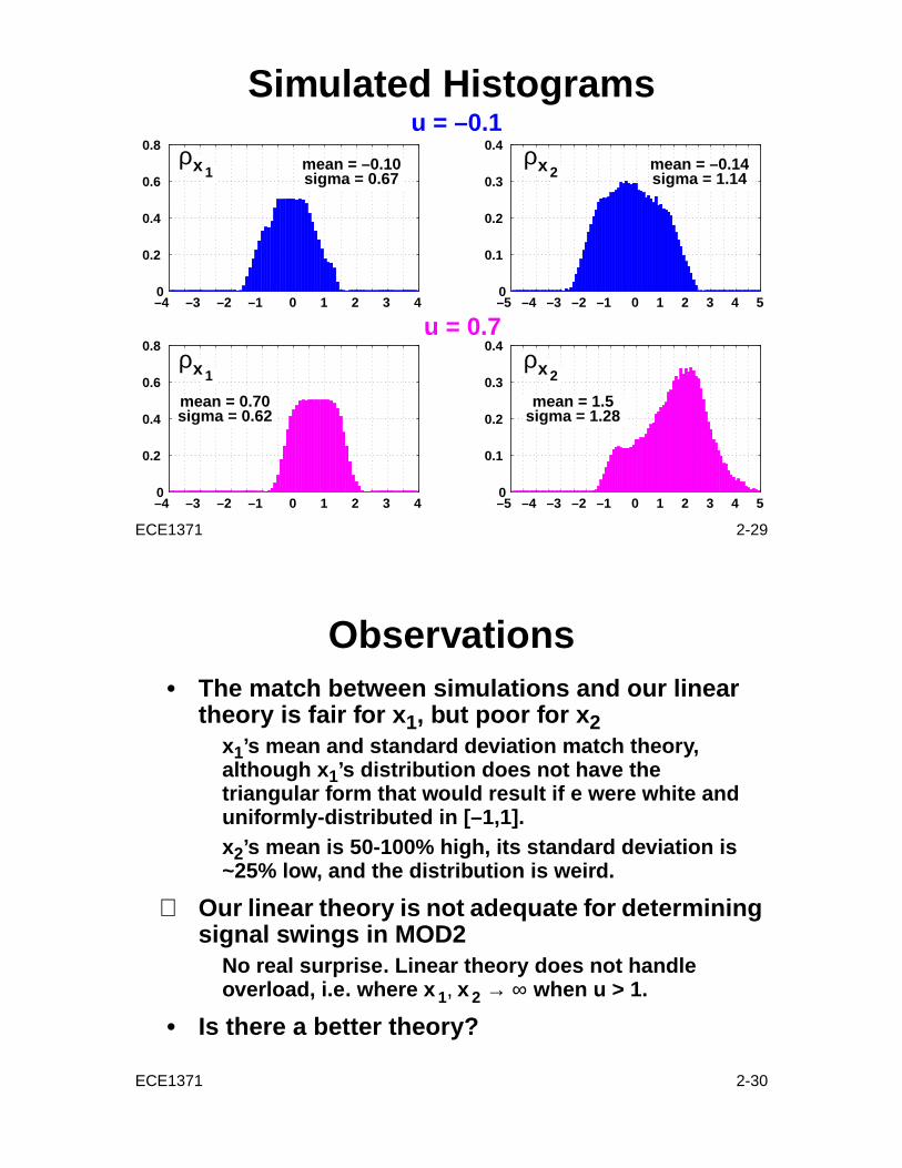
Simulated Histograms
–4 –3 –2 –1 0 1 2 3 40
0.2
0.4
0.6
0.8
–5 –4 –3 –2 –1 0 1 2 3 4 50
0.1
0.2
0.3
0.4
–4 –3 –2 –1 0 1 2 3 40
0.2
0.4
0.6
0.8
–5 –4 –3 –2 –1 0 1 2 3 4 50
0.1
0.2
0.3
0.4
ρx 2ρx 1
ρx 2ρx 1
mean = –0.10sigma = 0.67
mean = –0.14sigma = 1.14
mean = 0.70sigma = 0.62
mean = 1.5sigma = 1.28
u = –0.1
u = 0.7
ECE1371 2-30
Observations• The match between simulations and our linear
theory is fair for x1, but poor for x2x1’s mean and standard deviation match theory,although x1’s distribution does not have thetriangular form that would result if e were white anduniformly-distributed in [–1,1].x2’s mean is 50-100% high, its standard deviation is~25% low, and the distribution is weird.
⇒ Our linear theory is not adequate for determiningsignal swings in MOD2
No real surprise. Linear theory does not handleoverload, i.e. where when u > 1.
• Is there a better theory?
x 1 x 2, ∞→
ECE1371 2-31
MOD2’s Dynamics• Second-order DT system with a step nonlinearity
For a constant input, follow parabolictrajectories in state-space, except when crossing thestep (i.e. when x2 changes sign).
• If the image is inside the original, we have apositively-invariant set
x 1 n( ) x 2 n( ),( )
-2 -1 0 1 2-3
-2
-1
0
1
2
3
4
-2 -1 0 1 2-3
-2
-1
0
1
2
3
4
x1 x1
x2x2
A
B
C
D
D+
D–
A
B–C
B+
u 1 π⁄=
One clock tickparabolictrajectory
ECE1371 2-32
MOD2 DC-Input State Bounds• By computing the state-space trajectories with u
as a parameter, Hein & Zakhor [ISCAS 1991]determined invariant sets analytically andthereby arrived at the following bounds for
:
• Note that the bound on asIn order to use this formula for dynamic-rangescaling, we need to restrict the u to a fraction of full-scale.
u 1≤x 1 u 2+≤
x 25 u–( )2
8 1 u–( )------------------------≤
x 2 ∞→ u 1→
ECE1371 2-33
Comparison with Simulation
0 0.2 0.4 0.6 0.8 1 0
2
4
6
8
10
u
x 2 ∞
x 1 ∞
simulation
analyticboundsx
∞
ECE1371 2-34
State Bounds for MOD2Nonlinear Theory
So we do have some better theory, but it
1 Appears to be conservativeEspecially for u close to FS.
2 Predicts that x2 can be arbitrarily largeSimulations indicate that x2 does get big as ,but not quite as big as the theory predicts.
3 Assumes the input is constantAttempts to generalize the method for arbitraryinputs could only prove stability for .Inputs with have been constructed whichdrive MOD2 unstable!
u 1→
u ∞ 0.1<u ∞ 0.3=
ECE1371 2-35
Example Hostile Input
• Input signal chosen to cause the comparator inMOD2 to make bad decisions
Requires knowledge of MOD2’s internal state.
• Inputs like this are unlikely to occur in practice
u ∞ 0.3=
0 100 200
–0.3
0
0.3
u
ECE1371 2-36
Scaled MOD2• Take and
The first integrator should not saturate.The second integrator will not saturate for dc inputsup to –3 dBFS and possibly as high as –1 dBFS.
• Our scaled version of MOD2 is then
x 1 ∞ 3= x 2 ∞ 9=
Q1z−1
zz−1
U V9
Omit since
X1’ X2’
sgn(ky ) = sgn(y )1/91/3
1/3 1/3
ECE1371 2-37
First Integrator (INT1)Shared Input/Reference Caps
• How do we determine C?
Vu
2•v
1
1 2
2•v
Vx1
2•v
1
1 2
2•v
+Vref –Vref
C
C
3C
3C
+Vref –Vref zz−1
U
3/1
3/1
V
CM of Vref = CM of Vu
ECE1371 2-38
kT/C Noise
• Fact: Regardless of the value of R, the mean-square value of the voltage on C is
where k = 1.38 ×10⁻²³ J/K is Boltzmann’sconstant and T is the temperature in Kelvin
The ms noise charge is .
R C vn
v n2 kT
C--------=
qn2 C2v n
2 kTC= =
ECE1371 2-39
Derivation of kT/C Noise• Equipartition of Energy physical principle:
“In a system at thermal equilibrium, the averageenergy associated with any degree of freedom iskT.”
This applies to the kinetic energy of atoms (alongeach axis of motion), vibrational energy in moleculesand to the potential energy in electrical components.
• Fact: The energy stored in a capacitor is
• So, according to equipartition, ,or
12
12---CV 2
12---CV 2 1
2---kT=
V 2 kTC
--------=
ECE1371 2-40
Implications for an SC Integrator• Each charge/discharge operation has a random
componentThe amplifier plays a role during phase 2, but we’llassume that the noise in both phases is just kT/C.We’ll revisit this assumption in Lecture 10.
• For a given cap, these random components areessentially uncorrelated, so the noise is white
2 1
1 2C1
q1
q22
1 qt = q1+q2
qt2 q1
2 q22+ 2kT C1= =
q12 q2
2 kT C1= =
ECE1371 2-41
Integrator Implications (cont’d)• This noise charge is equivalent to a noise
voltage with ms value added tothe input of the integrator:
• This noise power is spread uniformly over allfrequencies from 0 to
⇒ The power in the band is
v n2 2kT C1⁄=
zz−1
C1 C2
vn
f s 2⁄
0 f B,[ ] v n2 OSR⁄
ECE1371 2-42
Differential Noise
• Twice as many switched caps⇒ twice as much noise power
• The input-referred noise power in our differentialintegrator is
Second Integrator (INT2)Separate Input and Feedback Caps
Vx12
1
Vx22
1C
9C
9C
zz−1
X1
9/1
3/1
V1•v
2
1•v
3C
C
2
21•v1•v
Vref
1
23C
1
CM of Vx1 CM of Vref CM of op amp input
ECE1371 2-45
INT2 Absolute Capacitor Sizes• In-band noise of second integrator is greatly
attenuated
⇒ Capacitor sizes not dictated by thermal noise
• Charge injection errors and desired ratioaccuracy set absolute size
A reasonable size for a small cap is currently ~10 fF.
ωBπ
OSR--------------=
INT1 gain @ pb edge: A 1 3⁄ωB
---------- OSR3π
--------------= =
INT2 noise attenuation: OSR A2⋅> 106≈
ECE1371 2-46
Behavioral Schematic
ECE1371 2-47
VerificationOpen-loop verification
1 Loop filter
2 ComparatorSince MOD2 is a 1-bit system, all that can go wrongis the polarity and the timing. Usually the timing ischecked by (1), so this verification step is notneeded.
Closed-loop verification
3 Swing of internal states
4 Spectrum: SQNR, STF gain
5 Sensitivity, start-up, overload recovery, …
ECE1371 2-48
Loop-Filter Check— Theory• Open the feedback loop, set u = 0 and drive an
impulse through the feedback path
• If x2 is as predicted then the loop filter is correctAt least for the feedback signal, which implies thatthe NTF will be as designed.
Hey! You Cheated!• An impulse is {1,0,0,…}, but a binary DAC can
only output ±1, i.e. it cannot produce a 0
Q: So how can we determine the impulse responseof the loop filter through simulation?
A: Do two simulations: one with v = {–1,–1,–1,…}and one with v = {+1,–1,–1,…}.Then take the difference.According to superposition, the result is theresponse to v = {2,0,0,…}, so divide by 2.
To keep the integrator states from growing tooquickly, you could also use v = {–1,–1,+1,–1,…} andthen v = {+1,–1,+1,–1,…}.
Implementation Summary1 Choose a viable SC topology and manually
verify timing
2 Do dynamic-range scalingYou now have a set of capacitor ratios.Verify operation: loop filter, timing, swing, spectrum.
3 Determine absolute capacitor sizesVerify noise.
4 Determine op-amp specs and construct atransistor-level schematic
Verify everything.
5 Layout, fab, debug, document, get customers,sell by the millions, go public, …
ECE1371 2-55
NLCOTD: Kelvin Connection• How to measure V accurately when is a
significant fraction of R?
• Use dedicated wires for sensingAlso called a “4-wire,” “Force/Sense” or “Current/Potential” connection. Common in power supplies.
Rp ωLp+
R V+
–
Rp Lp
ECE1371 2-56
Differential vs. Single-Ended• Differential is more complicated and has more
caps and more noise ⇒ single-ended is better?
• Same capacitor area ⇒ same SNRDifferential is generally preferred due to rejection ofeven-order distortion and common-mode noise/interference.
C/2±V
±VC/2
±VC
SNR 2V( )2 2⁄4kT C 2⁄( )⁄-------------------------------- CV 2
4kT------------= = SNR V 2 2⁄
2kT C⁄-------------------- CV 2
4kT------------= =
ECE1371 2-57
Double-Sampled Input
• Doubles the effective input signal
• Allows C1 to be the size for the same SNR
• Doubles the sampling rate of the signal, therebyeasing AAF further
2
1
2
1C1
Vu
C12
21
1
1 4⁄
ECE1371 2-58
Shared vs. Separate Input Caps• Separate caps ⇒ More noise:
• But using separate caps allows input CM to bedifferent from reference CM, and so is oftenpreferred in a general-purpose ADC
C1
C2
C
V1
V2
V1 input:
V2 input:
V2 gain / V1 gain:
vn2 referred to V1:
Total noise referred to V1:
v n12 2kT C1⁄=
v n22 2kT C2⁄=
C2 C1⁄
v n2C2 C1⁄
2kT C1⁄( ) 1 C2 C1⁄+( )
ECE1371 2-59
Signal-Dependent Ref. Loading• Another practical concern is the current draw
from the reference
• If the reference current is signal-related,harmonic distortion can result
Vref α ωtsin
Vref,actual
ADC OutputV in
V ref 1 ε ωtsin–( )---------------------------------------------
V in
V ref----------- 1 ε ωtsin+( )≈∝
ECE1371 2-60
Shared Caps and Ref. Loading
C
Vu
2•v
1
1 2
2•v
2•v
1
1 2
2•v
+Vref –Vref
C
C
+Vref –Vref
C
q+Vref
Vu
qC V ref V u 2⁄–( ) , v +1=
C V ref V u 2⁄+( ) , v –1=
=
ECE1371 2-61
Thus
• If , then also containsa component at and thus I contains acomponent at .
• Since , the signal-dependent reference current in our circuit canproduce 3rd-harmonic distortion
Also, the load presented to the driving circuit isdependent on v and this noisy load can causetrouble.
• With separate caps, the reference current issignal-independent
Yet another reason for using separate caps.
I CT---- V ref v V⋅ u 2⁄–( )=
u A ωutsin= v u error+=ωu
ω 2ωu=
ADC Output V in 1 ε ωtsin+( )∝
ECE1371 2-62
Unipolar Reference
• Be careful of the timing of v relative to theintegration phase!
1
2
1
2
1•v + 2•v
Vref
1 2
v (n ) v (n +1)
1 2
C
q = v •C•Vref
v DAC
ECE1371 2-63
Single-Ended InputShared Caps
Vu
2•v
1
1 2
2•v
1•v
1
2 2
1•v
C
C
Vref
Vref
Full-scale range of Vu is[0,Vref].
1 2
v (n ) v (n +1)
1 2
ECE1371 2-64
Homework #2Construct a differential switched-capacitorimplementation of MOD2 using ideal elements andverify it. Your circuit should accept a single-endedinput and use a unipolar 1-V reference.
Scale the circuit such that [0,2] V is the half-scaleinput range ([–1,3] V would be the full-scale inputrange) and such that the op amp swing is 0.5 Vp,diff at–6 dBFS.
Choose capacitor values such that the SNR with a–6 dBFS input should be ~90 dB when OSR = 256.
ECE1371 2-65
What You Learned TodayAnd what the homework should solidify
1 MOD2 implementation
2 Switched-capacitor integratorSC summer & DAC too


![[Howard Schreier] PROC SQL by Example Using SQL w(BookFi.org)](https://static.documents.pub/doc/80x56/55cf992b550346d0339bfb2b/howard-schreier-proc-sql-by-example-using-sql-wbookfiorg.jpg)


![DC-to-DC Switching-Regulator Insights—Achieving Longer ... · By Sridhar Gurram [sridhar.gurram@analog.com] Oliver Brennan [oliver.brennan@analog.com] Tim Wilkerson [tim.wilkerson@analog.com]](https://static.documents.pub/doc/80x56/61219f3deb944c100772c8e6/dc-to-dc-switching-regulator-insightsaachieving-longer-by-sridhar-gurram-sridhargurram.jpg)


