48


Examples
1
EMPro 2012October 2012
Examples

Examples
2
© Agilent Technologies, Inc. 2000-20115301 Stevens Creek Blvd., Santa Clara, CA 95052 USANo part of this documentation may be reproduced in any form or by any means (includingelectronic storage and retrieval or translation into a foreign language) without prioragreement and written consent from Agilent Technologies, Inc. as governed by UnitedStates and international copyright laws.
AcknowledgmentsMentor Graphics is a trademark of Mentor Graphics Corporation in the U.S. and othercountries. Microsoft®, Windows®, MS Windows®, Windows NT®, and MS-DOS® are U.S.registered trademarks of Microsoft Corporation. Pentium® is a U.S. registered trademarkof Intel Corporation. PostScript® and Acrobat® are trademarks of Adobe SystemsIncorporated. UNIX® is a registered trademark of the Open Group. Java™ is a U.S.trademark of Sun Microsystems, Inc. SystemC® is a registered trademark of OpenSystemC Initiative, Inc. in the United States and other countries and is used withpermission. MATLAB® is a U.S. registered trademark of The Math Works, Inc.. HiSIM2source code, and all copyrights, trade secrets or other intellectual property rights in and tothe source code in its entirety, is owned by Hiroshima University and STARC.
The following third-party libraries are used by the NlogN Momentum solver:
"This program includes Metis 4.0, Copyright © 1998, Regents of the University ofMinnesota", http://www.cs.umn.edu/~metis , METIS was written by George Karypis([email protected]).
Intel@ Math Kernel Library, http://www.intel.com/software/products/mkl
SuperLU_MT version 2.0 - Copyright © 2003, The Regents of the University of California,through Lawrence Berkeley National Laboratory (subject to receipt of any requiredapprovals from U.S. Dept. of Energy). All rights reserved. SuperLU Disclaimer: THISSOFTWARE IS PROVIDED BY THE COPYRIGHT HOLDERS AND CONTRIBUTORS "AS IS"AND ANY EXPRESS OR IMPLIED WARRANTIES, INCLUDING, BUT NOT LIMITED TO, THEIMPLIED WARRANTIES OF MERCHANTABILITY AND FITNESS FOR A PARTICULAR PURPOSEARE DISCLAIMED. IN NO EVENT SHALL THE COPYRIGHT OWNER OR CONTRIBUTORS BELIABLE FOR ANY DIRECT, INDIRECT, INCIDENTAL, SPECIAL, EXEMPLARY, ORCONSEQUENTIAL DAMAGES (INCLUDING, BUT NOT LIMITED TO, PROCUREMENT OFSUBSTITUTE GOODS OR SERVICES; LOSS OF USE, DATA, OR PROFITS; OR BUSINESSINTERRUPTION) HOWEVER CAUSED AND ON ANY THEORY OF LIABILITY, WHETHER INCONTRACT, STRICT LIABILITY, OR TORT (INCLUDING NEGLIGENCE OR OTHERWISE)ARISING IN ANY WAY OUT OF THE USE OF THIS SOFTWARE, EVEN IF ADVISED OF THEPOSSIBILITY OF SUCH DAMAGE.
AMD Version 2.2 - AMD Notice: The AMD code was modified. Used by permission. AMDcopyright: AMD Version 2.2, Copyright © 2007 by Timothy A. Davis, Patrick R. Amestoy,and Iain S. Duff. All Rights Reserved. AMD License: Your use or distribution of AMD or anymodified version of AMD implies that you agree to this License. This library is freesoftware; you can redistribute it and/or modify it under the terms of the GNU LesserGeneral Public License as published by the Free Software Foundation; either version 2.1 ofthe License, or (at your option) any later version. This library is distributed in the hopethat it will be useful, but WITHOUT ANY WARRANTY; without even the implied warranty ofMERCHANTABILITY or FITNESS FOR A PARTICULAR PURPOSE. See the GNU LesserGeneral Public License for more details. You should have received a copy of the GNULesser General Public License along with this library; if not, write to the Free SoftwareFoundation, Inc., 51 Franklin St, Fifth Floor, Boston, MA 02110-1301 USA Permission ishereby granted to use or copy this program under the terms of the GNU LGPL, providedthat the Copyright, this License, and the Availability of the original version is retained onall copies.User documentation of any code that uses this code or any modified version ofthis code must cite the Copyright, this License, the Availability note, and "Used bypermission." Permission to modify the code and to distribute modified code is granted,provided the Copyright, this License, and the Availability note are retained, and a noticethat the code was modified is included. AMD Availability:http://www.cise.ufl.edu/research/sparse/amd
UMFPACK 5.0.2 - UMFPACK Notice: The UMFPACK code was modified. Used by permission.UMFPACK Copyright: UMFPACK Copyright © 1995-2006 by Timothy A. Davis. All RightsReserved. UMFPACK License: Your use or distribution of UMFPACK or any modified versionof UMFPACK implies that you agree to this License. This library is free software; you canredistribute it and/or modify it under the terms of the GNU Lesser General Public Licenseas published by the Free Software Foundation; either version 2.1 of the License, or (atyour option) any later version. This library is distributed in the hope that it will be useful,but WITHOUT ANY WARRANTY; without even the implied warranty of MERCHANTABILITYor FITNESS FOR A PARTICULAR PURPOSE. See the GNU Lesser General Public License formore details. You should have received a copy of the GNU Lesser General Public Licensealong with this library; if not, write to the Free Software Foundation, Inc., 51 Franklin St,Fifth Floor, Boston, MA 02110-1301 USA Permission is hereby granted to use or copy thisprogram under the terms of the GNU LGPL, provided that the Copyright, this License, andthe Availability of the original version is retained on all copies. User documentation of any

Examples
3
code that uses this code or any modified version of this code must cite the Copyright, thisLicense, the Availability note, and "Used by permission." Permission to modify the codeand to distribute modified code is granted, provided the Copyright, this License, and theAvailability note are retained, and a notice that the code was modified is included.UMFPACK Availability: http://www.cise.ufl.edu/research/sparse/umfpack UMFPACK(including versions 2.2.1 and earlier, in FORTRAN) is available athttp://www.cise.ufl.edu/research/sparse . MA38 is available in the Harwell SubroutineLibrary. This version of UMFPACK includes a modified form of COLAMD Version 2.0,originally released on Jan. 31, 2000, also available athttp://www.cise.ufl.edu/research/sparse . COLAMD V2.0 is also incorporated as a built-infunction in MATLAB version 6.1, by The MathWorks, Inc. http://www.mathworks.com .COLAMD V1.0 appears as a column-preordering in SuperLU (SuperLU is available athttp://www.netlib.org ). UMFPACK v4.0 is a built-in routine in MATLAB 6.5. UMFPACK v4.3is a built-in routine in MATLAB 7.1.
Errata The ADS product may contain references to "HP" or "HPEESOF" such as in filenames and directory names. The business entity formerly known as "HP EEsof" is now partof Agilent Technologies and is known as "Agilent EEsof". To avoid broken functionality andto maintain backward compatibility for our customers, we did not change all the namesand labels that contain "HP" or "HPEESOF" references.
Warranty The material contained in this document is provided "as is", and is subject tobeing changed, without notice, in future editions. Further, to the maximum extentpermitted by applicable law, Agilent disclaims all warranties, either express or implied,with regard to this documentation and any information contained herein, including but notlimited to the implied warranties of merchantability and fitness for a particular purpose.Agilent shall not be liable for errors or for incidental or consequential damages inconnection with the furnishing, use, or performance of this document or of anyinformation contained herein. Should Agilent and the user have a separate writtenagreement with warranty terms covering the material in this document that conflict withthese terms, the warranty terms in the separate agreement shall control.
Technology Licenses The hardware and/or software described in this document arefurnished under a license and may be used or copied only in accordance with the terms ofsuch license. Portions of this product include the SystemC software licensed under OpenSource terms, which are available for download at http://systemc.org/ . This software isredistributed by Agilent. The Contributors of the SystemC software provide this software"as is" and offer no warranty of any kind, express or implied, including without limitationwarranties or conditions or title and non-infringement, and implied warranties orconditions merchantability and fitness for a particular purpose. Contributors shall not beliable for any damages of any kind including without limitation direct, indirect, special,incidental and consequential damages, such as lost profits. Any provisions that differ fromthis disclaimer are offered by Agilent only.
Restricted Rights Legend U.S. Government Restricted Rights. Software and technicaldata rights granted to the federal government include only those rights customarilyprovided to end user customers. Agilent provides this customary commercial license inSoftware and technical data pursuant to FAR 12.211 (Technical Data) and 12.212(Computer Software) and, for the Department of Defense, DFARS 252.227-7015(Technical Data - Commercial Items) and DFARS 227.7202-3 (Rights in CommercialComputer Software or Computer Software Documentation).
Examples
4
Antenna . . . . . . . . . . . . . . . . . . . . . . . . . . . . . . . . . . . . . . . . . . . . . . . . . . . . . . . . . . . . . . 5 Microstrip Dipole Antenna . . . . . . . . . . . . . . . . . . . . . . . . . . . . . . . . . . . . . . . . . . . . . . . . . 6 Microstrip Patch Antenna . . . . . . . . . . . . . . . . . . . . . . . . . . . . . . . . . . . . . . . . . . . . . . . . . 8 Patch Antenna with TNC Connector . . . . . . . . . . . . . . . . . . . . . . . . . . . . . . . . . . . . . . . . . . 11
Waveguide and Component . . . . . . . . . . . . . . . . . . . . . . . . . . . . . . . . . . . . . . . . . . . . . . . . . 13 Scanning Microwave Microscopy Experiment . . . . . . . . . . . . . . . . . . . . . . . . . . . . . . . . . . . . 14 Coaxial Waveguide Low Pass Filter . . . . . . . . . . . . . . . . . . . . . . . . . . . . . . . . . . . . . . . . . . 18 Magic Tee . . . . . . . . . . . . . . . . . . . . . . . . . . . . . . . . . . . . . . . . . . . . . . . . . . . . . . . . . . . . 21 Waveguide Power Divider . . . . . . . . . . . . . . . . . . . . . . . . . . . . . . . . . . . . . . . . . . . . . . . . . 23 Waveguide to Coaxial Transition . . . . . . . . . . . . . . . . . . . . . . . . . . . . . . . . . . . . . . . . . . . . 25
Planar RF Component . . . . . . . . . . . . . . . . . . . . . . . . . . . . . . . . . . . . . . . . . . . . . . . . . . . . . 27 Differential Vias . . . . . . . . . . . . . . . . . . . . . . . . . . . . . . . . . . . . . . . . . . . . . . . . . . . . . . . . 28 Low Pass Filter . . . . . . . . . . . . . . . . . . . . . . . . . . . . . . . . . . . . . . . . . . . . . . . . . . . . . . . . 30 LTCC Balun . . . . . . . . . . . . . . . . . . . . . . . . . . . . . . . . . . . . . . . . . . . . . . . . . . . . . . . . . . . 32 Microstrip Line . . . . . . . . . . . . . . . . . . . . . . . . . . . . . . . . . . . . . . . . . . . . . . . . . . . . . . . . 34
Eigenmode Solver . . . . . . . . . . . . . . . . . . . . . . . . . . . . . . . . . . . . . . . . . . . . . . . . . . . . . . . . 36 Eigenmode Solver on a DC-SIR Cylinder . . . . . . . . . . . . . . . . . . . . . . . . . . . . . . . . . . . . . . 37
General Examples . . . . . . . . . . . . . . . . . . . . . . . . . . . . . . . . . . . . . . . . . . . . . . . . . . . . . . . . 38 Agilent Phone . . . . . . . . . . . . . . . . . . . . . . . . . . . . . . . . . . . . . . . . . . . . . . . . . . . . . . . . . 39 Agilent Phone with Phantom . . . . . . . . . . . . . . . . . . . . . . . . . . . . . . . . . . . . . . . . . . . . . . . 41 QFN Package . . . . . . . . . . . . . . . . . . . . . . . . . . . . . . . . . . . . . . . . . . . . . . . . . . . . . . . . . 43 RCS of Aircraft . . . . . . . . . . . . . . . . . . . . . . . . . . . . . . . . . . . . . . . . . . . . . . . . . . . . . . . . 45

Examples
5
AntennaThis section provides information about the following topics:
Microstrip Dipole Antenna (example)Microstrip Patch Antenna (example)Patch Antenna with TNC Connector (example)
Examples
6
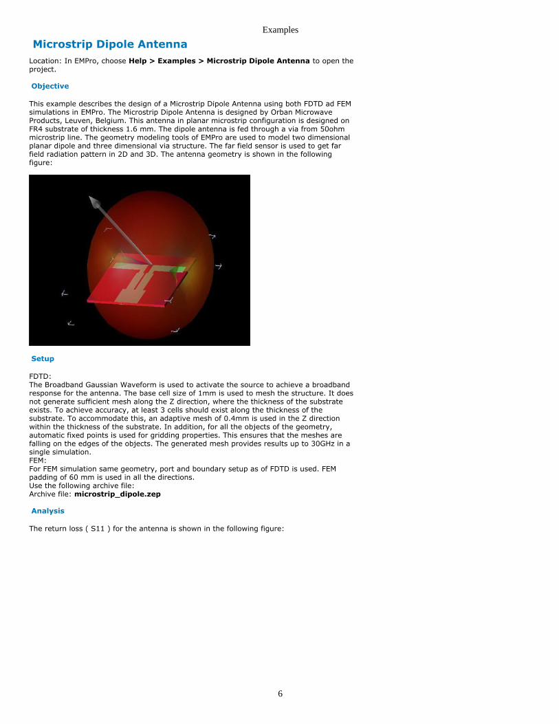
Microstrip Dipole AntennaLocation: In EMPro, choose Help > Examples > Microstrip Dipole Antenna to open theproject.
Objective
This example describes the design of a Microstrip Dipole Antenna using both FDTD ad FEMsimulations in EMPro. The Microstrip Dipole Antenna is designed by Orban MicrowaveProducts, Leuven, Belgium. This antenna in planar microstrip configuration is designed onFR4 substrate of thickness 1.6 mm. The dipole antenna is fed through a via from 50ohmmicrostrip line. The geometry modeling tools of EMPro are used to model two dimensionalplanar dipole and three dimensional via structure. The far field sensor is used to get farfield radiation pattern in 2D and 3D. The antenna geometry is shown in the followingfigure:
Setup
FDTD:The Broadband Gaussian Waveform is used to activate the source to achieve a broadbandresponse for the antenna. The base cell size of 1mm is used to mesh the structure. It doesnot generate sufficient mesh along the Z direction, where the thickness of the substrateexists. To achieve accuracy, at least 3 cells should exist along the thickness of thesubstrate. To accommodate this, an adaptive mesh of 0.4mm is used in the Z directionwithin the thickness of the substrate. In addition, for all the objects of the geometry,automatic fixed points is used for gridding properties. This ensures that the meshes arefalling on the edges of the objects. The generated mesh provides results up to 30GHz in asingle simulation.FEM:For FEM simulation same geometry, port and boundary setup as of FDTD is used. FEMpadding of 60 mm is used in all the directions.Use the following archive file:Archive file: microstrip_dipole.zep
Analysis
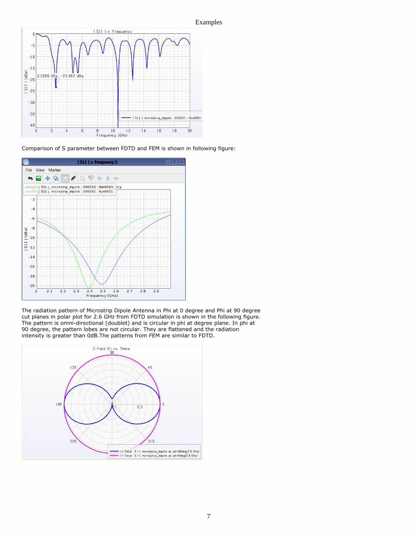
The return loss ( S11 ) for the antenna is shown in the following figure:
Examples
7
Comparison of S parameter between FDTD and FEM is shown in following figure:
The radiation pattern of Microstrip Dipole Antenna in Phi at 0 degree and Phi at 90 degreecut planes in polar plot for 2.6 GHz from FDTD simulation is shown in the following figure.The pattern is omni-directional (doublet) and is circular in phi at degree plane. In phi at90 degree, the pattern lobes are not circular. They are flattened and the radiationintensity is greater than 0dB.The patterns from FEM are similar to FDTD.
Examples
8
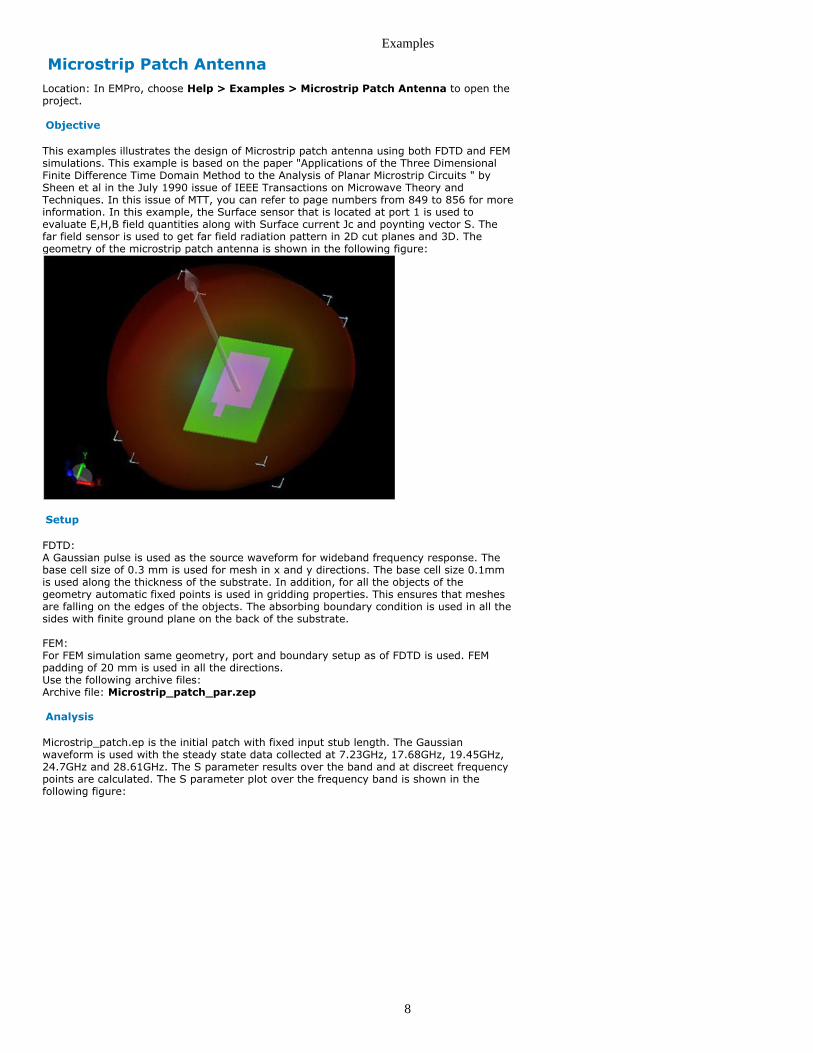
Microstrip Patch AntennaLocation: In EMPro, choose Help > Examples > Microstrip Patch Antenna to open theproject.
Objective
This examples illustrates the design of Microstrip patch antenna using both FDTD and FEMsimulations. This example is based on the paper "Applications of the Three DimensionalFinite Difference Time Domain Method to the Analysis of Planar Microstrip Circuits " bySheen et al in the July 1990 issue of IEEE Transactions on Microwave Theory andTechniques. In this issue of MTT, you can refer to page numbers from 849 to 856 for moreinformation. In this example, the Surface sensor that is located at port 1 is used toevaluate E,H,B field quantities along with Surface current Jc and poynting vector S. Thefar field sensor is used to get far field radiation pattern in 2D cut planes and 3D. Thegeometry of the microstrip patch antenna is shown in the following figure:
Setup
FDTD:A Gaussian pulse is used as the source waveform for wideband frequency response. Thebase cell size of 0.3 mm is used for mesh in x and y directions. The base cell size 0.1mmis used along the thickness of the substrate. In addition, for all the objects of thegeometry automatic fixed points is used in gridding properties. This ensures that meshesare falling on the edges of the objects. The absorbing boundary condition is used in all thesides with finite ground plane on the back of the substrate.
FEM:For FEM simulation same geometry, port and boundary setup as of FDTD is used. FEMpadding of 20 mm is used in all the directions.Use the following archive files:Archive file: Microstrip_patch_par.zep
Analysis
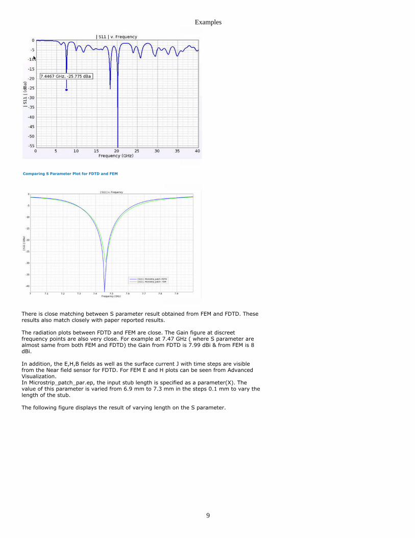
Microstrip_patch.ep is the initial patch with fixed input stub length. The Gaussianwaveform is used with the steady state data collected at 7.23GHz, 17.68GHz, 19.45GHz,24.7GHz and 28.61GHz. The S parameter results over the band and at discreet frequencypoints are calculated. The S parameter plot over the frequency band is shown in thefollowing figure:
Examples
9
Comparing S Parameter Plot for FDTD and FEM
There is close matching between S parameter result obtained from FEM and FDTD. Theseresults also match closely with paper reported results.
The radiation plots between FDTD and FEM are close. The Gain figure at discreetfrequency points are also very close. For example at 7.47 GHz ( where S parameter arealmost same from both FEM and FDTD) the Gain from FDTD is 7.99 dBi & from FEM is 8dBi.
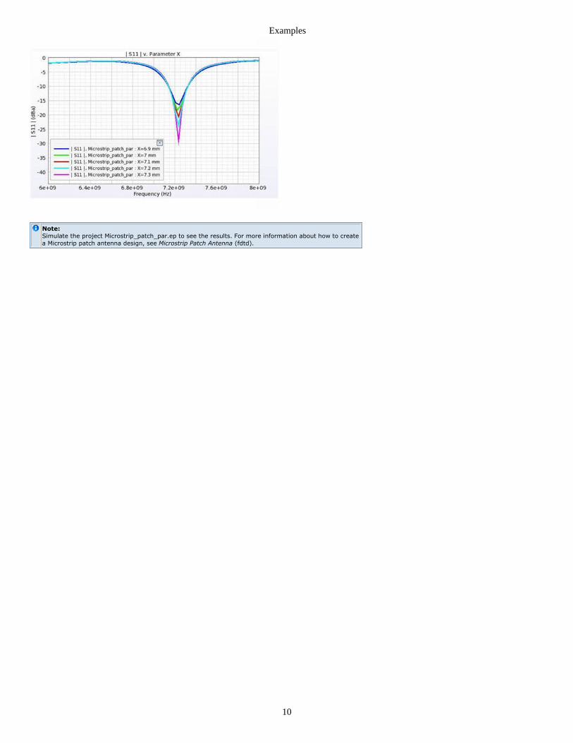
In addition, the E,H,B fields as well as the surface current J with time steps are visiblefrom the Near field sensor for FDTD. For FEM E and H plots can be seen from AdvancedVisualization.In Microstrip_patch_par.ep, the input stub length is specified as a parameter(X). Thevalue of this parameter is varied from 6.9 mm to 7.3 mm in the steps 0.1 mm to vary thelength of the stub.
The following figure displays the result of varying length on the S parameter.
Examples
10
Note:Simulate the project Microstrip_patch_par.ep to see the results. For more information about how to createa Microstrip patch antenna design, see Microstrip Patch Antenna (fdtd).
Examples
11
Patch Antenna with TNC ConnectorLocation: In EMPro, choose Help > Examples > Patch Antenna with TNC
Objective
This example illustrates the application of EMPro in designing a microstrip patch antennawith a TNC connector using FEM simulator. The TNC connector feeds the antenna fromback-side of the antenna. The design band is C band. The patch antenna is designed on asubstrate of 2.47 dielectric constant having thickness of 3.2 mm. The far field sensor isused to get far field radiation pattern in 2D cut planes and 3D.
The geometry of the microstrip patch antenna with TNC connector is shown in thefollowing figure:
Setup
FEM:FEM padding of 20 mm in upper Z, 0 mm in lower z and 30 mm in x and y directions areused. Absorbing boundary condition is used in all the directions.Waveguide port is used at the input of TNC connector.
Use the following archive files:Archive files: Patch_with_TNC.zep
Analysis
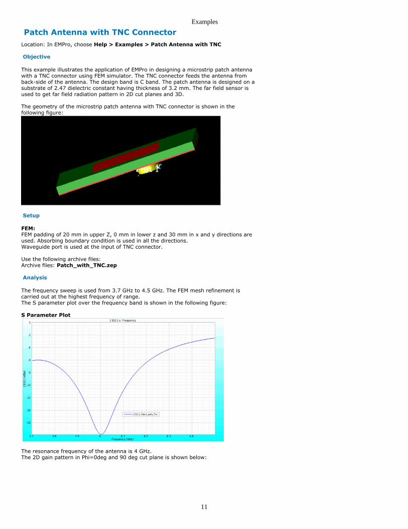
The frequency sweep is used from 3.7 GHz to 4.5 GHz. The FEM mesh refinement iscarried out at the highest frequency of range.The S parameter plot over the frequency band is shown in the following figure:
S Parameter Plot
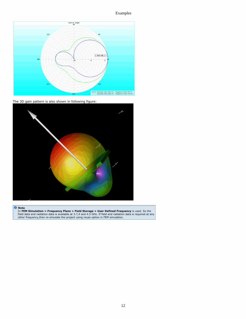
The resonance frequency of the antenna is 4 GHz.The 2D gain pattern in Phi=0deg and 90 deg cut plane is shown below:
Examples
12
The 3D gain pattern is also shown in following figure:
NoteIn FEM Simulation > Frequency Plans > Field Storage > User Defined Frequency is used. So thefield data and radiation data is available at 3.7,4 and 4.5 GHz. If field and radiation data is required at anyother frequency,then re-simulate the project using reuse option in FEM simulation.

Examples
13
Waveguide and ComponentThis section provides information about the following topics:
Scanning Microwave Microscopy Experiment (example)Magic Tee (example)Waveguide Power Divider (example)Waveguide to Coaxial Line Transition (example)Coaxial Waveguide Low Pass Filter (example)
Examples
14
Scanning Microwave Microscopy ExperimentLocation: In EMPro, choose Help > Examples > Scanning Microwave MicroscopyExperiment to open the project.
Objective
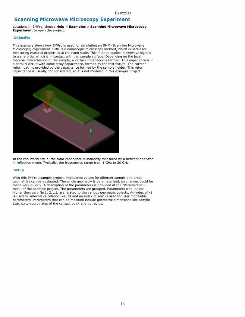
This example shows how EMPro is used for simulating an SMM (Scanning MicrowaveMicroscopy) experiment. SMM is a nanoscopic microscopy method, which is useful formeasuring material properties at the nano scale. This method applies microwave signalsto a sharp tip, which is in contact with the sample surface. Depending on the localmaterial characteristic of the sample, a certain impedance is formed. This impedance is ina parallel circuit with some stray capacitance, formed by the test fixture. The currentreturn path is provided by the capacitance formed by the sample holder. This returncapacitance is usually not considered, so it is not modeled in this example project.
In the real world setup, the total impedance is indirectly measured by a network analyzerin reflection mode. Typically, the frequencies range from 1 GHz to 20 GHz.
Setup
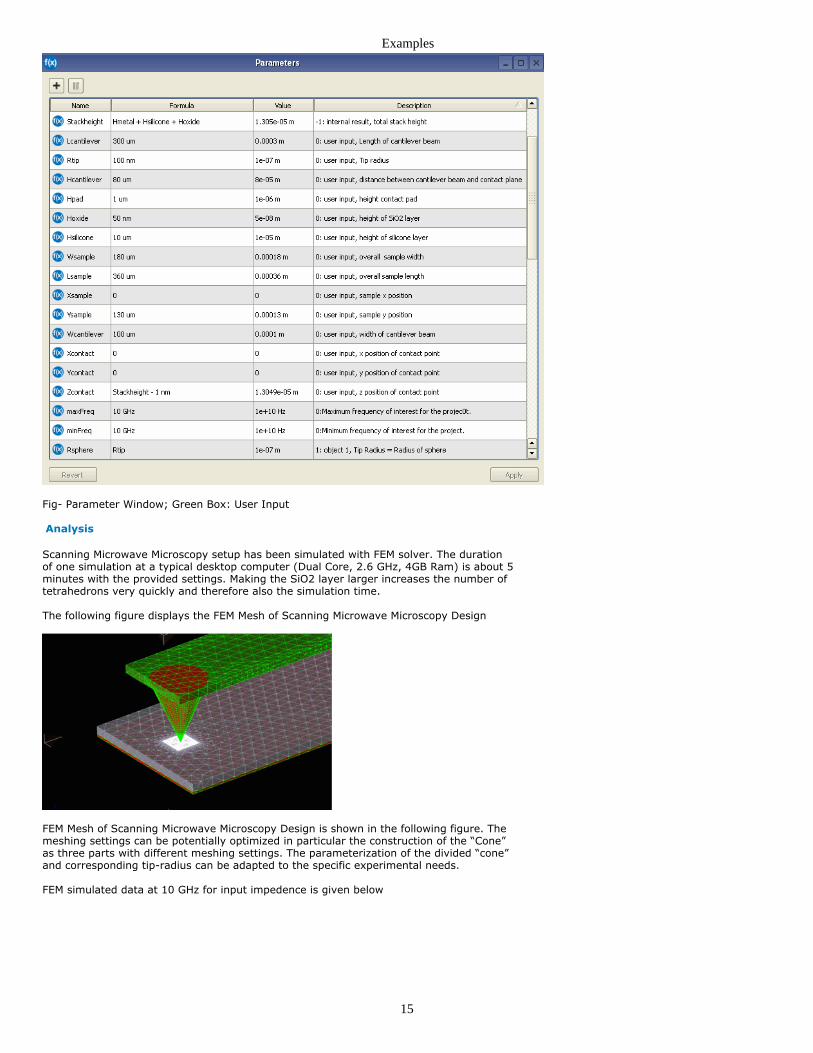
With this EMPro example project, impedance values for different sample and probegeometries can be evaluated. The whole geometry is parameterized, so changes could bemade very quickly. A description of the parameters is provided at the "Parameters" –menu of the example project. The parameters are grouped. Parameters with indiceshigher than zero (ie 1, 2, …), are related to the various geometric objects. An index of -1is used for internal calculation results and an index of zero is used for user modifiableparameters. Parameters that can be modified include geometric dimensions like samplesize, x,y,z-coordinates of the contact point and tip radius.
Examples
15
Fig- Parameter Window; Green Box: User Input
Analysis
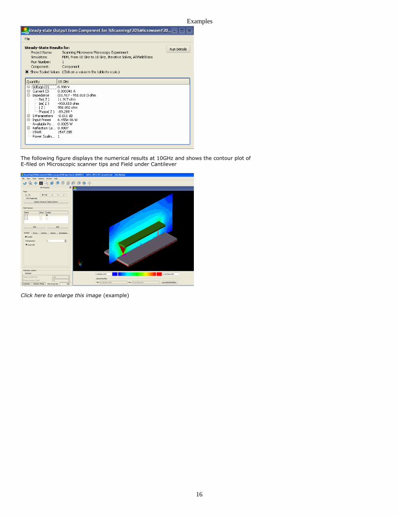
Scanning Microwave Microscopy setup has been simulated with FEM solver. The durationof one simulation at a typical desktop computer (Dual Core, 2.6 GHz, 4GB Ram) is about 5minutes with the provided settings. Making the SiO2 layer larger increases the number oftetrahedrons very quickly and therefore also the simulation time.
The following figure displays the FEM Mesh of Scanning Microwave Microscopy Design
FEM Mesh of Scanning Microwave Microscopy Design is shown in the following figure. Themeshing settings can be potentially optimized in particular the construction of the “Cone”as three parts with different meshing settings. The parameterization of the divided “cone”and corresponding tip-radius can be adapted to the specific experimental needs.
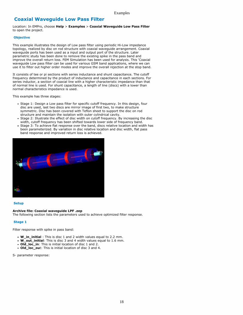
FEM simulated data at 10 GHz for input impedence is given below
Examples
16
The following figure displays the numerical results at 10GHz and shows the contour plot ofE-filed on Microscopic scanner tips and Field under Cantilever
Click here to enlarge this image (example)

Examples
17
Examples
18
Coaxial Waveguide Low Pass FilterLocation: In EMPro, choose Help > Examples > Coaxial Waveguide Low Pass Filterto open the project.
Objective
This example illustrates the design of Low pass filter using periodic Hi-Low impedancetopology, realized by disc on rod structure with coaxial waveguide arrangement. Coaxialwaveguide ports has been used as a input and output port of the structure. Laterparametric study has been done to remove the existing spike in the pass band andimprove the overall return loss. FEM Simulation has been used for analysis. This ‘Coaxialwaveguide Low pass filter can be used for various GSM band applications, where we canuse it to filter out higher order modes and improve the overall rejection at the stop band.
It consists of tee or pi sections with series inductance and shunt capacitance. The cutofffrequency determined by the product of inductance and capacitance in each sections. Forseries inductor, a section of coaxial line with a higher characteristic impedance than thatof normal line is used. For shunt capacitance, a length of line (discs) with a lower thannormal characteristics impedance is used.
This example has three stages:
Stage 1: Design a Low pass filter for specific cutoff frequency. In this design, fourdisc are used, last two discs are mirror image of first two, to make structuresymmetric. Disc has been covered with Teflon sheet to support the disc on rodstructure and maintain the isolation with outer cylindrical cavity.Stage 2: Illustrate the effect of disc width on cutoff frequency. By increasing the discwidth, cutoff frequency has been shifted towards lower side of frequency band.Stage 3: To achieve flat response over the band, discs relative location and width hasbeen parameterized. By variation in disc relative location and disc width, flat passband response and improved return loss is achieved.
Setup
Archive file: Coaxial waveguide LPF .zepThe following section lists the parameters used to achieve optimized filter response.
Stage 1
Filter response with spike in pass band:
W_in_initial : This is disc 1 and 2 width values equal to 2.2 mm.W_out_initial: This is disc 3 and 4 width values equal to 1.6 mm.Old_loc_in: This is initial location of disc 1 and 2.Old_loc_out: This is initial location of disc 3 and 4.
S- parameter response:
Examples
19
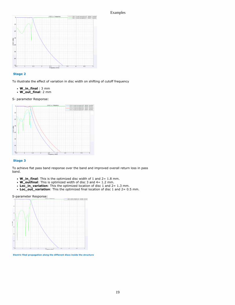
Stage 2
To illustrate the effect of variation in disc width on shifting of cutoff frequency
W_in_final : 3 mmW_out_final: 2 mm
S- parameter Response:
Stage 3
To achieve flat pass band response over the band and improved overall return loss in passband.
W_in_final: This is the optimized disc width of 1 and 2= 1.8 mm.W_outfinal: This is optimized width of disc 3 and 4= 1.2 mm.Loc_in_variation: This the optimized location of disc 1 and 2= 1.3 mm.Loc_out_variation: This the optimized final location of disc 1 and 2= 0.5 mm.
S-parameter Response:
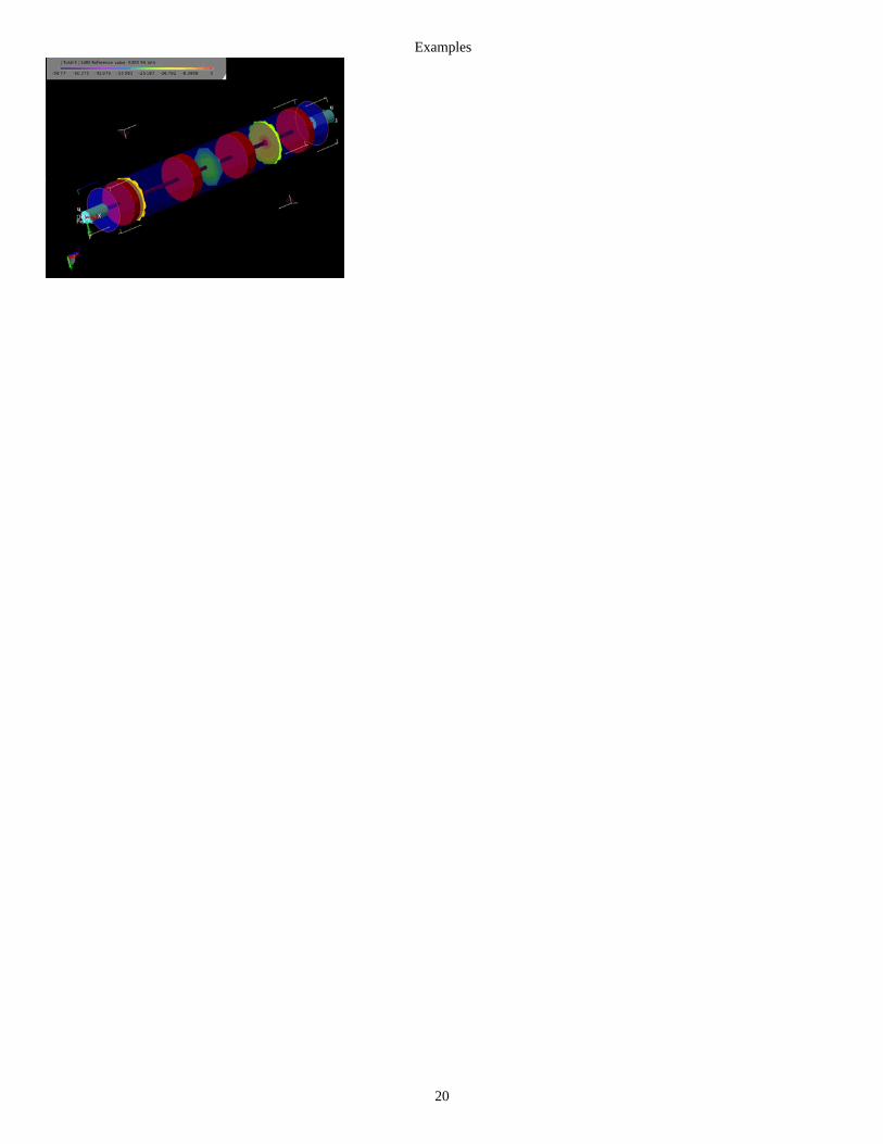
Electric filed propagation along the different discs inside the structure
Examples
20
Examples
21
Magic TeeLocation: In EMPro, choose Help > Examples > Magic Tee to open the project.
Objective
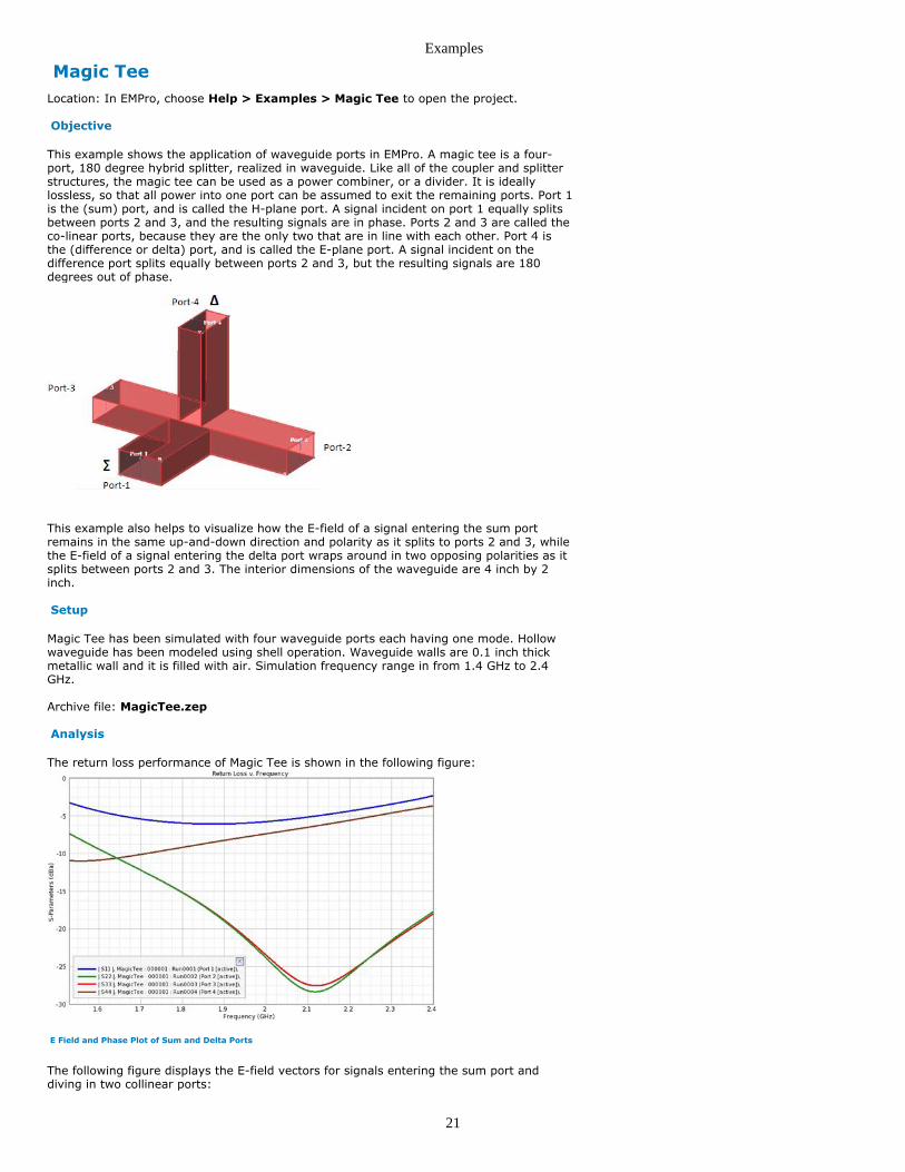
This example shows the application of waveguide ports in EMPro. A magic tee is a four-port, 180 degree hybrid splitter, realized in waveguide. Like all of the coupler and splitterstructures, the magic tee can be used as a power combiner, or a divider. It is ideallylossless, so that all power into one port can be assumed to exit the remaining ports. Port 1is the (sum) port, and is called the H-plane port. A signal incident on port 1 equally splitsbetween ports 2 and 3, and the resulting signals are in phase. Ports 2 and 3 are called theco-linear ports, because they are the only two that are in line with each other. Port 4 isthe (difference or delta) port, and is called the E-plane port. A signal incident on thedifference port splits equally between ports 2 and 3, but the resulting signals are 180degrees out of phase.
This example also helps to visualize how the E-field of a signal entering the sum portremains in the same up-and-down direction and polarity as it splits to ports 2 and 3, whilethe E-field of a signal entering the delta port wraps around in two opposing polarities as itsplits between ports 2 and 3. The interior dimensions of the waveguide are 4 inch by 2inch.
Setup
Magic Tee has been simulated with four waveguide ports each having one mode. Hollowwaveguide has been modeled using shell operation. Waveguide walls are 0.1 inch thickmetallic wall and it is filled with air. Simulation frequency range in from 1.4 GHz to 2.4GHz.
Archive file: MagicTee.zep
Analysis
The return loss performance of Magic Tee is shown in the following figure:
E Field and Phase Plot of Sum and Delta Ports
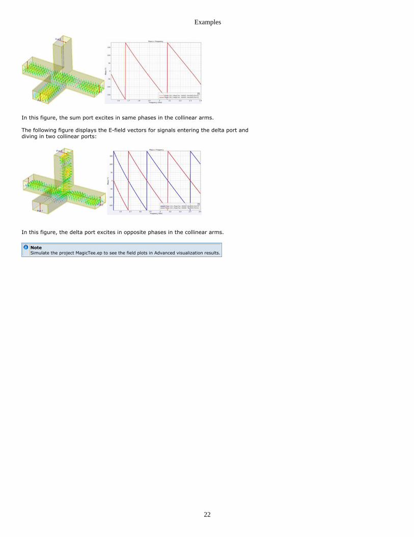
The following figure displays the E-field vectors for signals entering the sum port anddiving in two collinear ports:
Examples
22
In this figure, the sum port excites in same phases in the collinear arms.
The following figure displays the E-field vectors for signals entering the delta port anddiving in two collinear ports:
In this figure, the delta port excites in opposite phases in the collinear arms.
NoteSimulate the project MagicTee.ep to see the field plots in Advanced visualization results.
Examples
23
Waveguide Power DividerLocation: In EMPro, choose Help > Examples > Waveguide Power Divider
Objective
This example describes the design of waveguide power divider with waveguide ports usingFEM engine of EMPro.
Setup
The waveguide used in power divider is WR159. This is equal power divider with input armpower divided into two output arm each having equal -3dB power. The design band is Cband and a matching section is used to get return loss( S11) better than -10 dB between4.5 Ghz and 7.5 GHz.Archive files: Waveguide_power_divider.zep
Analysis
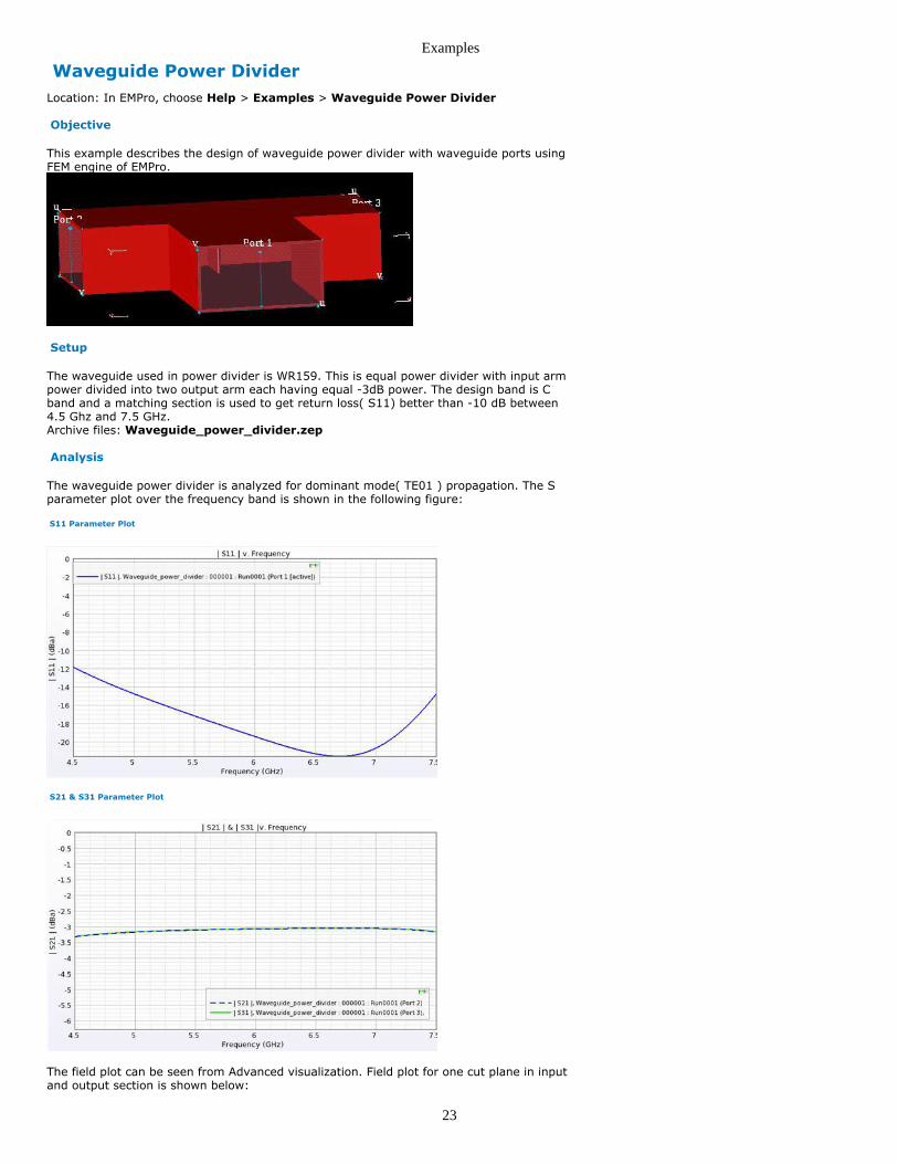
The waveguide power divider is analyzed for dominant mode( TE01 ) propagation. The Sparameter plot over the frequency band is shown in the following figure:
S11 Parameter Plot
S21 & S31 Parameter Plot
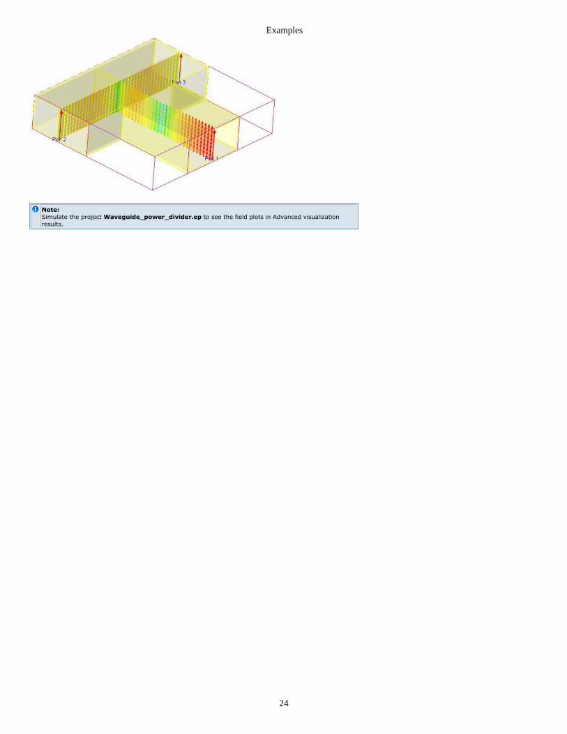
The field plot can be seen from Advanced visualization. Field plot for one cut plane in inputand output section is shown below:
Examples
24
Note:Simulate the project Waveguide_power_divider.ep to see the field plots in Advanced visualizationresults.
Examples
25
Waveguide to Coaxial TransitionLocation: In EMPro, choose Help > Examples > Waveguide to Coax.
Objective
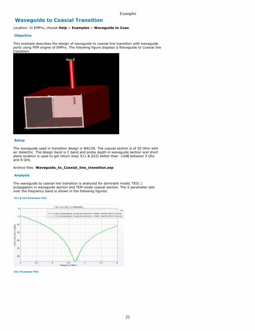
This example describes the design of waveguide to coaxial line transition with waveguideports using FEM engine of EMPro. The following figure displays a Waveguide to Coaxial linetransition:
Setup
The waveguide used in transition design is WR159. The coaxial section is of 50 Ohm withair dielectric. The design band is C band and probe depth in waveguide section and shortplane location is used to get return loss( S11 & S22) better than -10dB between 5 Ghzand 8 GHz.
Archive files: Waveguide_to_Coaxial_line_transition.zep
Analysis
The waveguide to coaxial line transition is analyzed for dominant mode( TE01 )propagation in waveguide section and TEM mode coaxial section. The S parameter plotover the frequency band is shown in the following figures:
S11 & S22 Parameter Plot
S21 Parameter Plot
Examples
26
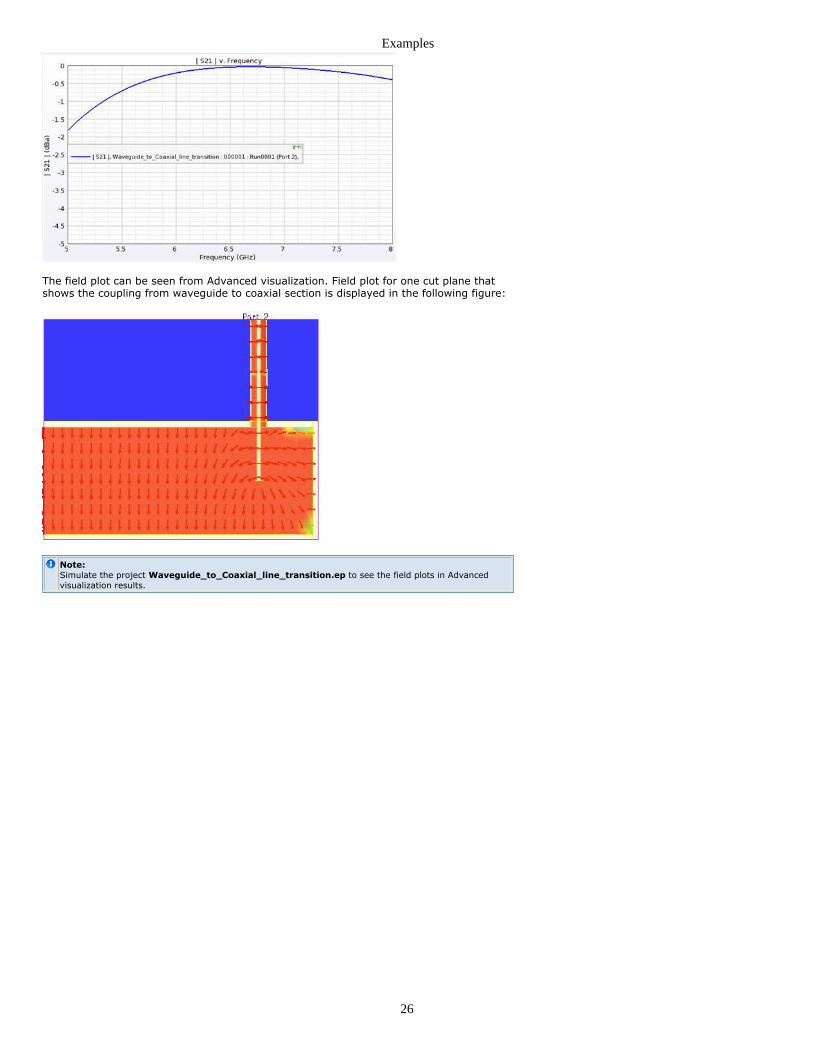
The field plot can be seen from Advanced visualization. Field plot for one cut plane thatshows the coupling from waveguide to coaxial section is displayed in the following figure:
Note:Simulate the project Waveguide_to_Coaxial_line_transition.ep to see the field plots in Advancedvisualization results.

Examples
27
Planar RF ComponentThis section provides information about the following topics:
Low Pass Filter (example)LTCC Balun (example)Microstrip Line (example)
Examples
28
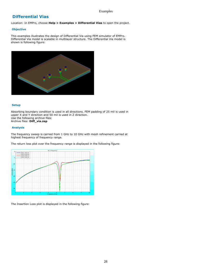
Differential ViasLocation: In EMPro, choose Help > Examples > Differential Vias to open the project.
Objective
This examples illustrates the design of Differential Via using FEM simulator of EMPro.Differential Via model is scalable in multilayer structure. The Differential Via model isshown is following figure:
Setup
Absorbing boundary condition is used in all directions. FEM padding of 25 mil is used inupper X and Y direction and 50 mil is used in Z direction.Use the following archive files:Archive files: Diff_via.zep
Analysis
The frequency sweep is carried from 1 GHz to 10 GHz with mesh refinement carried athighest frequency of frequency range.
The return loss plot over the frequency range is displayed in the following figure:
The Insertion Loss plot is displayed in the following figure:

Examples
29
NoteIn the Setup FEM Simulation window, access the Frequency Plan tab and choose User definedfrequency in Field Storage. The field data is available at 1,5 and 10 GHz. If field data is required at anyother frequency, again simulate the project by using reuse option in FEM simulation.
Examples
30
Low Pass FilterLocation: In EMPro, choose Help > Examples > Low Pass Filter to open the project.
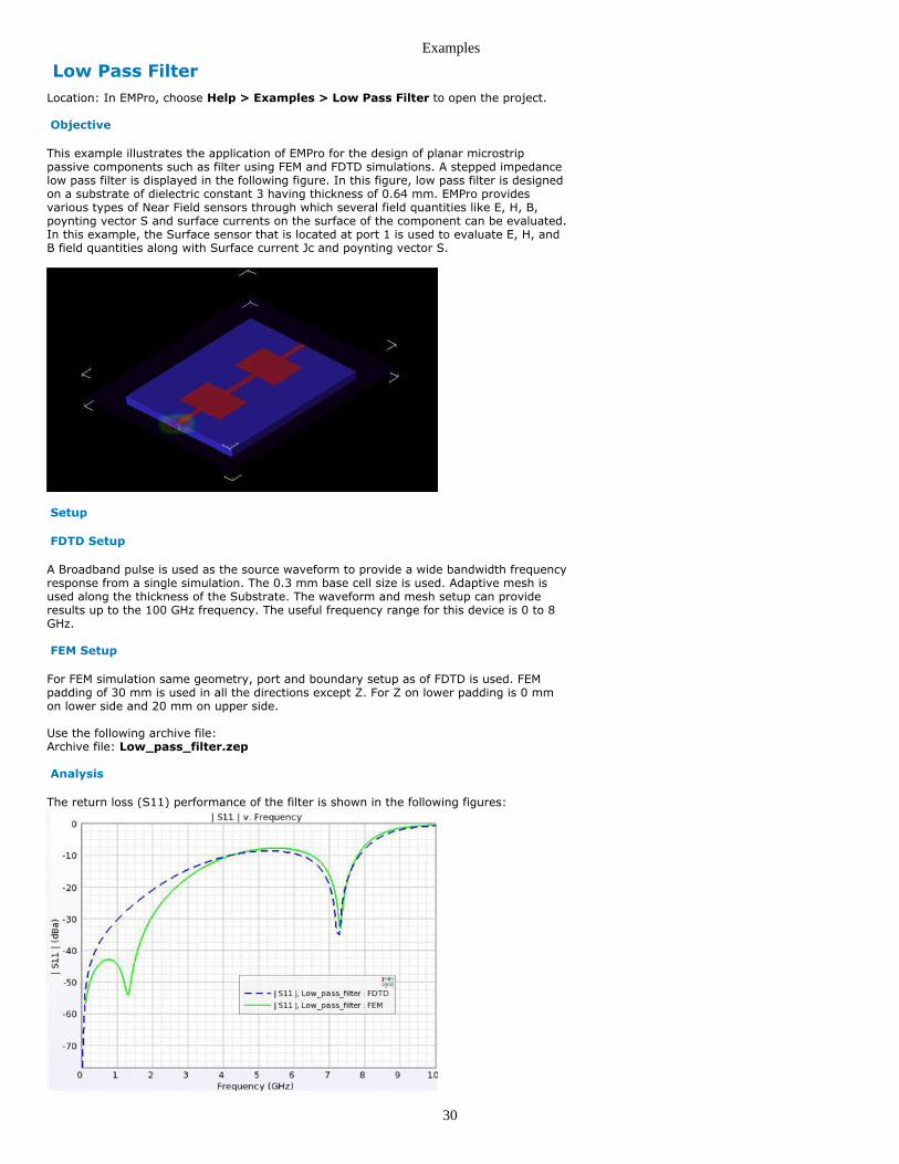
Objective
This example illustrates the application of EMPro for the design of planar microstrippassive components such as filter using FEM and FDTD simulations. A stepped impedancelow pass filter is displayed in the following figure. In this figure, low pass filter is designedon a substrate of dielectric constant 3 having thickness of 0.64 mm. EMPro providesvarious types of Near Field sensors through which several field quantities like E, H, B,poynting vector S and surface currents on the surface of the component can be evaluated.In this example, the Surface sensor that is located at port 1 is used to evaluate E, H, andB field quantities along with Surface current Jc and poynting vector S.
Setup
FDTD Setup
A Broadband pulse is used as the source waveform to provide a wide bandwidth frequencyresponse from a single simulation. The 0.3 mm base cell size is used. Adaptive mesh isused along the thickness of the Substrate. The waveform and mesh setup can provideresults up to the 100 GHz frequency. The useful frequency range for this device is 0 to 8GHz.
FEM Setup
For FEM simulation same geometry, port and boundary setup as of FDTD is used. FEMpadding of 30 mm is used in all the directions except Z. For Z on lower padding is 0 mmon lower side and 20 mm on upper side.
Use the following archive file:Archive file: Low_pass_filter.zep
Analysis
The return loss (S11) performance of the filter is shown in the following figures:
Examples
31
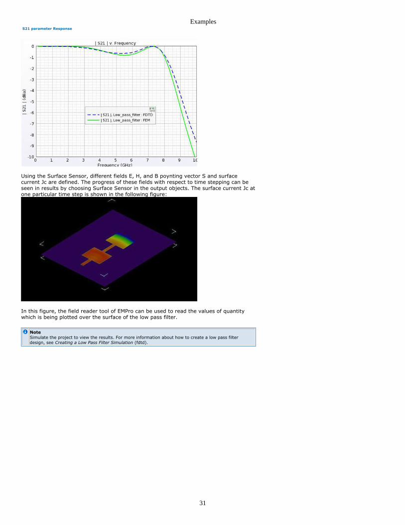
S21 parameter Response
Using the Surface Sensor, different fields E, H, and B poynting vector S and surfacecurrent Jc are defined. The progress of these fields with respect to time stepping can beseen in results by choosing Surface Sensor in the output objects. The surface current Jc atone particular time step is shown in the following figure:
In this figure, the field reader tool of EMPro can be used to read the values of quantitywhich is being plotted over the surface of the low pass filter.
NoteSimulate the project to view the results. For more information about how to create a low pass filterdesign, see Creating a Low Pass Filter Simulation (fdtd).
Examples
32
LTCC BalunLocation: In EMPro, choose Help > Examples > LTCC Balun to open the project.
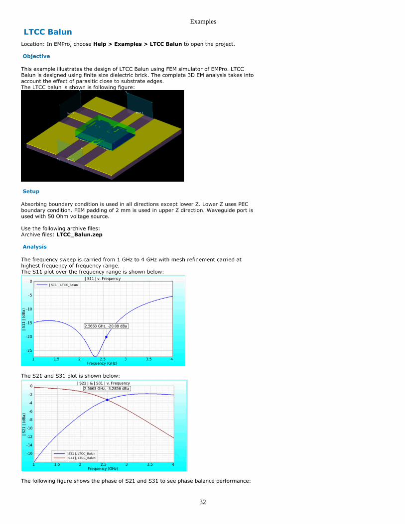
Objective
This example illustrates the design of LTCC Balun using FEM simulator of EMPro. LTCCBalun is designed using finite size dielectric brick. The complete 3D EM analysis takes intoaccount the effect of parasitic close to substrate edges.The LTCC balun is shown is following figure:
Setup
Absorbing boundary condition is used in all directions except lower Z. Lower Z uses PECboundary condition. FEM padding of 2 mm is used in upper Z direction. Waveguide port isused with 50 Ohm voltage source.
Use the following archive files:Archive files: LTCC_Balun.zep
Analysis
The frequency sweep is carried from 1 GHz to 4 GHz with mesh refinement carried athighest frequency of frequency range.The S11 plot over the frequency range is shown below:
The S21 and S31 plot is shown below:
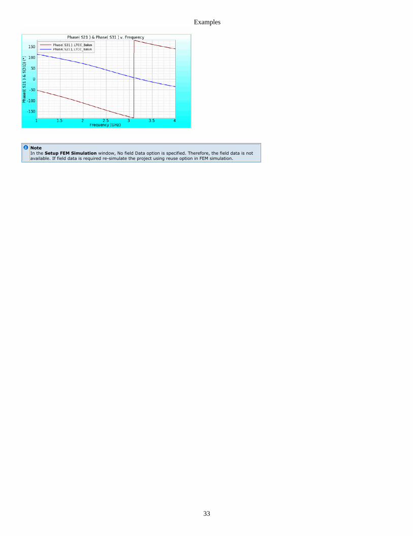
The following figure shows the phase of S21 and S31 to see phase balance performance:
Examples
33
NoteIn the Setup FEM Simulation window, No field Data option is specified. Therefore, the field data is notavailable. If field data is required re-simulate the project using reuse option in FEM simulation.
Examples
34
Microstrip LineLocation: In EMPro, choose Help > Examples > Microstrip Line 50 ohm to open theproject.
Objective
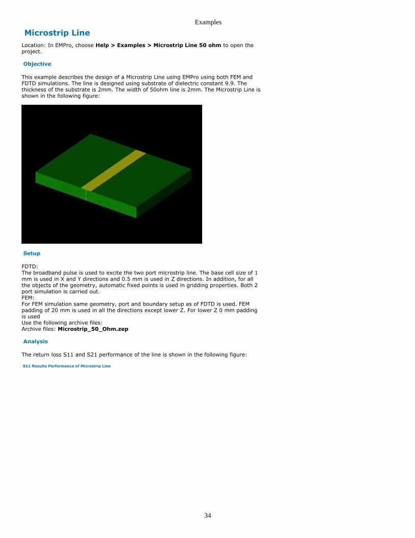
This example describes the design of a Microstrip Line using EMPro using both FEM andFDTD simulations. The line is designed using substrate of dielectric constant 9.9. Thethickness of the substrate is 2mm. The width of 50ohm line is 2mm. The Microstrip Line isshown in the following figure:
Setup
FDTD:The broadband pulse is used to excite the two port microstrip line. The base cell size of 1mm is used in X and Y directions and 0.5 mm is used in Z directions. In addition, for allthe objects of the geometry, automatic fixed points is used in gridding properties. Both 2port simulation is carried out.FEM:For FEM simulation same geometry, port and boundary setup as of FDTD is used. FEMpadding of 20 mm is used in all the directions except lower Z. For lower Z 0 mm paddingis usedUse the following archive files:Archive files: Microstrip_50_Ohm.zep
Analysis
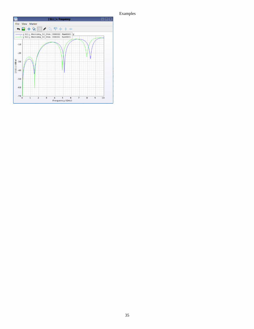
The return loss S11 and S21 performance of the line is shown in the following figure:
S11 Results Performance of Microstrip Line
Examples
35

Examples
36
Eigenmode SolverThis section provides information about the following topics:
Eigenmode Solver on a DC-SIR Cylinder (example)
Examples
37
Eigenmode Solver on a DC-SIR CylinderLocation: In EMPro, choose Help > Examples > Eigenmode Solver on a DC-SIRCylinder to open the project.
Objective
In this example, a double coaxial stepped impedance resonator (DC-SIR) is simulated.Currently, EMPro does not support cylindrical boundaries. For cylindrical or other non-rectangle cavities, it is important to put a rectangular metal background to avoid externalartificial cavities between the metal walls and FEM boundaries.
Setup
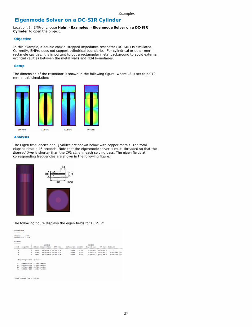
The dimension of the resonator is shown in the following figure, where L3 is set to be 10mm in this simulation:
Analysis
The Eigen frequencies and Q values are shown below with copper metals. The totalelapsed time is 46 seconds. Note that the eigenmode solver is multi-threaded so that theElapsed time is shorter than the CPU time in each solving pass. The eigen fields atcorresponding frequencies are shown in the following figure:
The following figure displays the eigen fields for DC-SIR:

Examples
38
General ExamplesThis section provides information about the following topics:
Agilent Phone (example)Agilent Phone with Phantom (example)QFN Package (example)RCS of Aircraft (example)Twisted Wire Pair (fdtd)
Examples
39
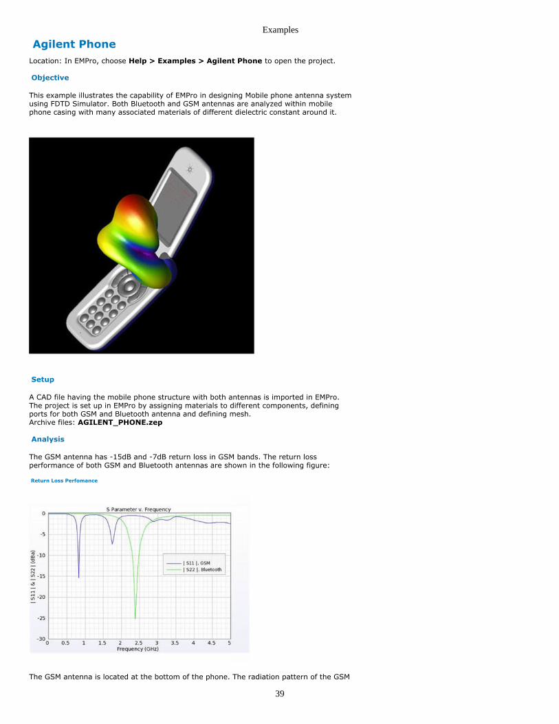
Agilent PhoneLocation: In EMPro, choose Help > Examples > Agilent Phone to open the project.
Objective
This example illustrates the capability of EMPro in designing Mobile phone antenna systemusing FDTD Simulator. Both Bluetooth and GSM antennas are analyzed within mobilephone casing with many associated materials of different dielectric constant around it.
Setup
A CAD file having the mobile phone structure with both antennas is imported in EMPro.The project is set up in EMPro by assigning materials to different components, definingports for both GSM and Bluetooth antenna and defining mesh.Archive files: AGILENT_PHONE.zep
Analysis
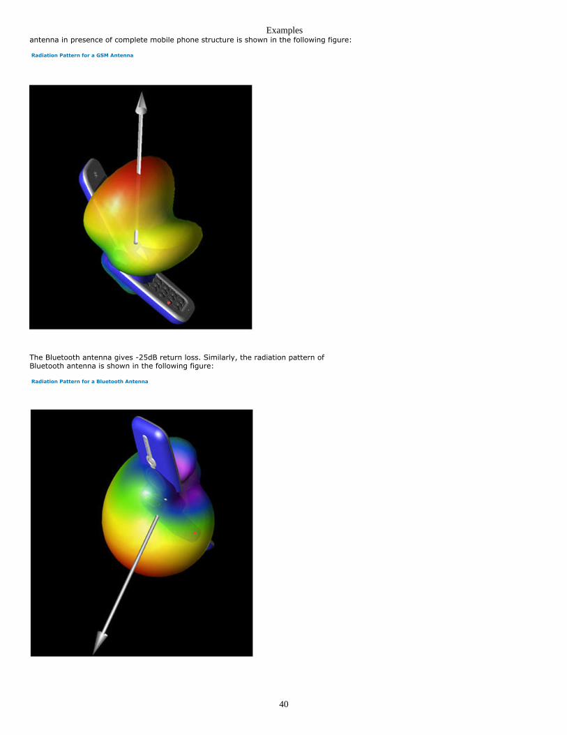
The GSM antenna has -15dB and -7dB return loss in GSM bands. The return lossperformance of both GSM and Bluetooth antennas are shown in the following figure:
Return Loss Perfomance
The GSM antenna is located at the bottom of the phone. The radiation pattern of the GSM
Examples
40
antenna in presence of complete mobile phone structure is shown in the following figure:
Radiation Pattern for a GSM Antenna
The Bluetooth antenna gives -25dB return loss. Similarly, the radiation pattern ofBluetooth antenna is shown in the following figure:
Radiation Pattern for a Bluetooth Antenna
Examples
41
Agilent Phone with PhantomLocation: In EMPro, choose Help > Examples > Agilent Phone with Phantom to openthe projects.
Objective
This example illustrates the SAR calculation capability of EMPro using FDTD simulator. Themobile phone structure with radiating GSM antenna is analyzed in the presence of ahuman head structure to calculate the SAR maximum and average data.
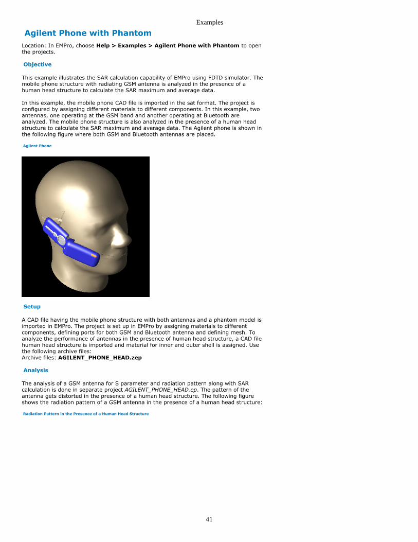
In this example, the mobile phone CAD file is imported in the sat format. The project isconfigured by assigning different materials to different components. In this example, twoantennas, one operating at the GSM band and another operating at Bluetooth areanalyzed. The mobile phone structure is also analyzed in the presence of a human headstructure to calculate the SAR maximum and average data. The Agilent phone is shown inthe following figure where both GSM and Bluetooth antennas are placed.
Agilent Phone
Setup
A CAD file having the mobile phone structure with both antennas and a phantom model isimported in EMPro. The project is set up in EMPro by assigning materials to differentcomponents, defining ports for both GSM and Bluetooth antenna and defining mesh. Toanalyze the performance of antennas in the presence of human head structure, a CAD filehuman head structure is imported and material for inner and outer shell is assigned. Usethe following archive files:Archive files: AGILENT_PHONE_HEAD.zep
Analysis
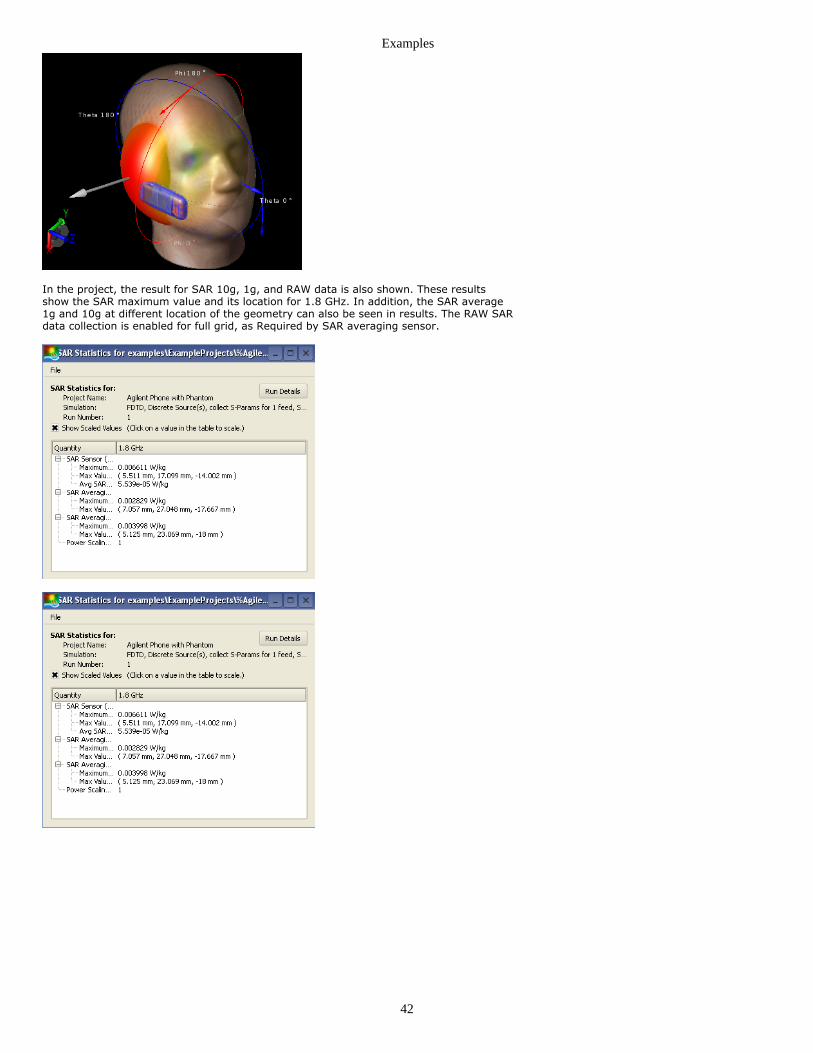
The analysis of a GSM antenna for S parameter and radiation pattern along with SARcalculation is done in separate project AGILENT_PHONE_HEAD.ep. The pattern of theantenna gets distorted in the presence of a human head structure. The following figureshows the radiation pattern of a GSM antenna in the presence of a human head structure:
Radiation Pattern in the Presence of a Human Head Structure
Examples
42
In the project, the result for SAR 10g, 1g, and RAW data is also shown. These resultsshow the SAR maximum value and its location for 1.8 GHz. In addition, the SAR average1g and 10g at different location of the geometry can also be seen in results. The RAW SARdata collection is enabled for full grid, as Required by SAR averaging sensor.
Examples
43
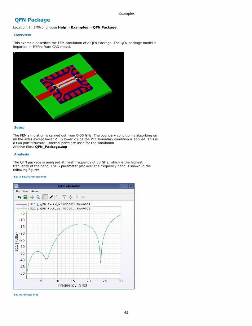
QFN PackageLocation: In EMPro, choose Help > Examples > QFN Package.
Overview
This example describes the FEM simulation of a QFN Package. The QFN package model isimported in EMPro from CAD model.
Setup
The FEM simulation is carried out from 0-30 GHz. The boundary condition is absorbing onall the sides except lower Z. In lower Z side the PEC boundary condition is applied. This isa two port structure. Internal ports are used for the simulationArchive files: QFN_Package.zep
Analysis
The QFN package is analyzed at mesh frequency of 30 GHz, which is the highestfrequency of the band. The S parameter plot over the frequency band is shown in thefollowing figure:
S11 & S22 Parameter Plot
S21 Parameter Plot
Examples
44
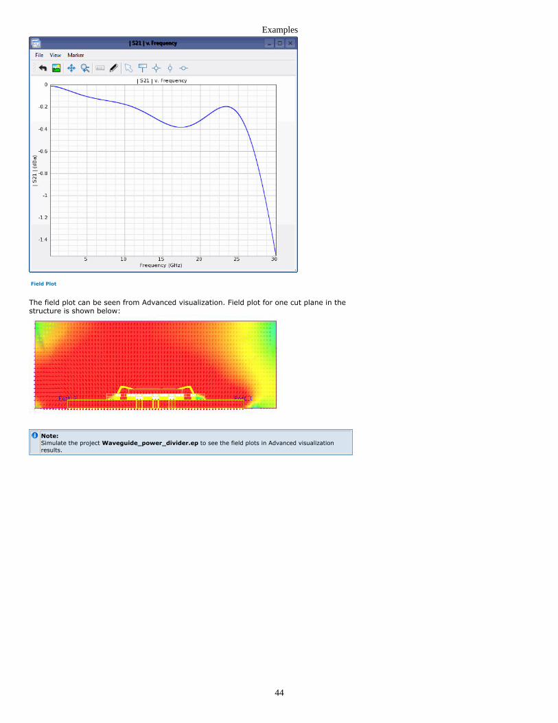
Field Plot
The field plot can be seen from Advanced visualization. Field plot for one cut plane in thestructure is shown below:
Note:Simulate the project Waveguide_power_divider.ep to see the field plots in Advanced visualizationresults.
Examples
45
RCS of AircraftLocation: In EMPro, choose Help > Examples > Example Projects > RCS of Aircraftto open the project.
Objective
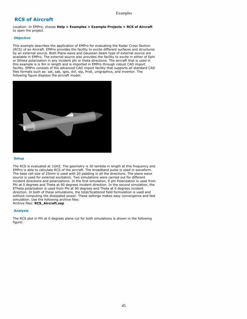
This example describes the application of EMPro for evaluating the Radar Cross Section(RCS) of an Aircraft. EMPro provides the facility to excite different surfaces and structuresby an external source. Both Plane wave and Gaussian beam type of external source areavailable in EMPro. The external source also provides the facility to excite in either of Ephior Etheta polarization in any incident phi or theta directions. The aircraft that is used inthis example is is 9m in length and is imported in EMPro through robust CAD importfacility. EMPro consists of the advanced CAD import facility that supports all standard CADfiles formats such as: sat, sab, iges, dxf, stp, ProE, unigraphics, and inventor. Thefollowing figure displays the aircraft model:
Setup
The RCS is evaluated at 1GHZ. The geometry is 30 lambda in length at this frequency andEMPro is able to calculate RCS of the aircraft. The broadband pulse is used in waveform.The base cell size of 25mm is used with 20 padding in all the directions. The plane wavesource is used for external excitation. Two simulations were carried out for differentincident directions and polarizations. In the first simulation, E phi Polarization is used fromPhi at 0 degrees and Theta at 90 degrees incident direction. In the second simulation, theETheta polarization is used from Phi at 90 degrees and Theta at 0 degrees incidentdirection. In both of these simulations, the total/Scattered field formulation is used andwithout computing the dissipated power. These settings makes easy convergence and fastsimulation. Use the following archive files:Archive files: RCS_Aircraft.zep
Analysis
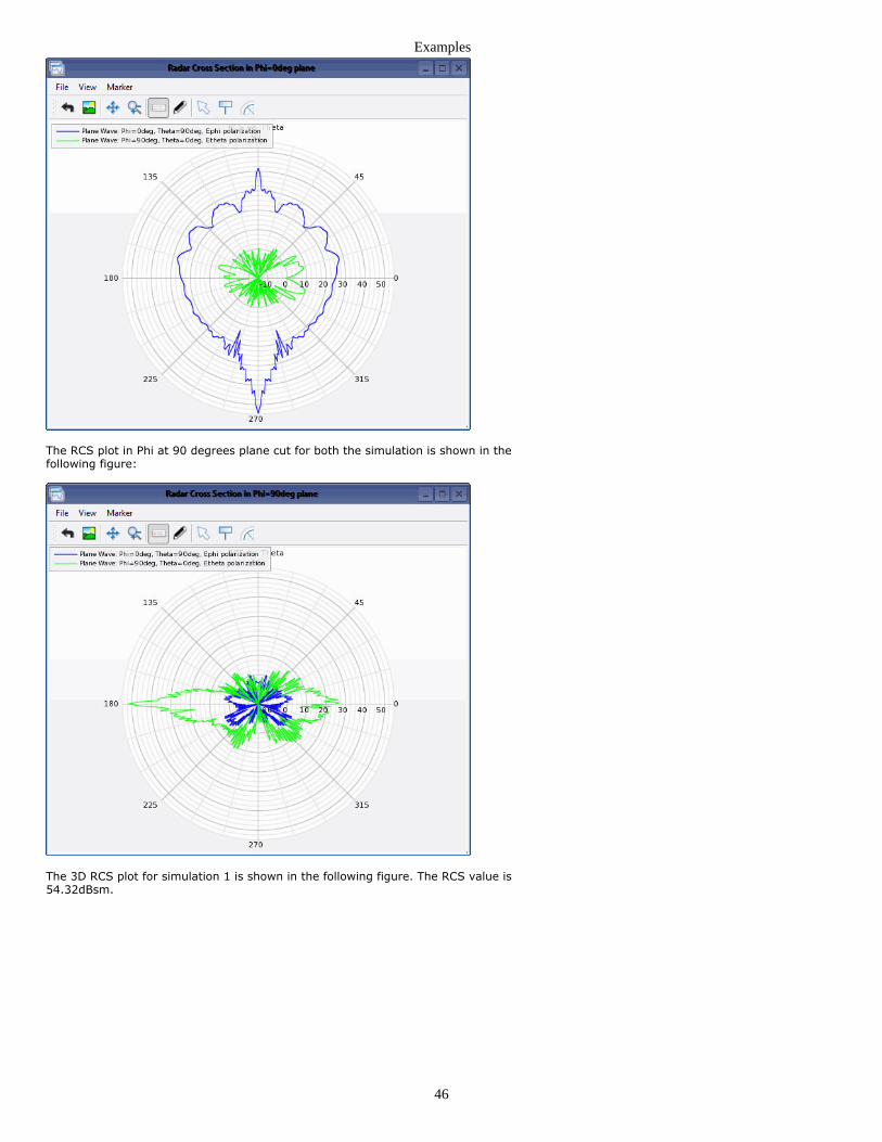
The RCS plot in Phi at 0 degrees plane cut for both simulations is shown in the followingfigure:
Examples
46
The RCS plot in Phi at 90 degrees plane cut for both the simulation is shown in thefollowing figure:
The 3D RCS plot for simulation 1 is shown in the following figure. The RCS value is54.32dBsm.
Examples
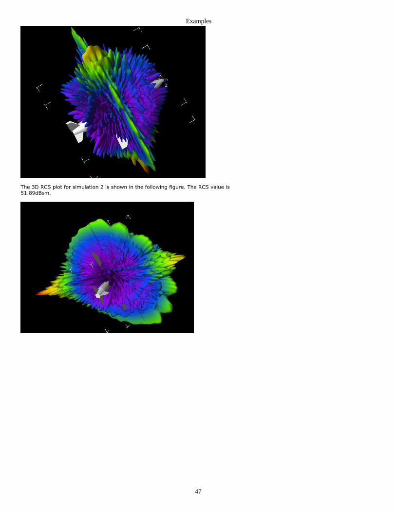
47
The 3D RCS plot for simulation 2 is shown in the following figure. The RCS value is51.89dBsm.


