Digital Controller Eases Design Of Interleaved PFC For Multi-kilowatt Converters
by Rosario Attanasio, Giuseppe Di Caro, Sebastiano Messina, and Marco Torrisi, STMicroelectronics,
Schaumburg, Ill. and Catania, Italy
In power supply applications requiring higher power up to and beyond a kilowatt, the design of power factor correction (PFC) boost converters using interleaved stages rather than a single stage becomes advantageous.
That’s because the combination of multiple interleaved stages allows for use of smaller, lower-profile
components including smaller filter components. However, the controller IC options that have been available to date have required specialized design and programming skills in order to implement PFC at the kilowatt level,
while also imposing performance restrictions due to bandwidth limitations associated with digital control of the
compensation loop.
To overcome these difficulties, a new digital controller has been developed that is suitable for multi-channel interleaved PFC topologies operating in continuous conduction mode (CCM). The operation and application of
this IC, the STNRGPF01, are presented in this article.
The main characteristics and specifications of the controller are provided in the first section. The control structure is then discussed: this is based on a semi-digital control scheme where the time critical functions such
as fast overcurrent protection and input current control are performed using analog parts to attain precise,
cycle-by-cycle regulation.
All the non-time-critical functions, such as multiplier, feed-forward compensation, voltage protections and
voltage control loop are implemented digitally. The experimental results for a 3-kW three-channel interleaved
PFC prototype, provided in the last section of the article, show the suitability of the proposed approach and the benefits of combining digital and analog control techniques.
Benefits And Challenges Of Interleaved PFC
In applications where the required power is greater than 1 kW and where the form factor is a design constraint,
interleaved converters are often used. Interleaving of PFCs consists of using two or more active single-switch stages (Fig. 1), each rated for a lower power, instead of a single stage rated for the full power and more
challenging to design.
Fig. 1. Interleaved boost PFC with N active channels.
The main advantages of an interleaved converter are ripple cancellation, reduction of magnetic component size and volume, lower EMI and better thermal management. By interleaving, the equivalent inductor current ripple
is reduced and it is completely cancelled for some precise values of duty cycle (i.e. D = 0.5 for two-channel boost; D = 0.33 and D = 0.66 for three-channels PFCs).
The ripple-cancellation effect, which is a consequence of operating the paralleled stages with a phase shift equal
to 360 degrees divided by the number of stages, is also very important not only for EMI and power density but also for efficiency.
Few analog ICs are available for the implementation of interleaved topologies. Most of them limit the designer
to the use of two interleaved PFC stages operated in critical conduction mode (CrCM) with constant on time (COT) control. This allows the use of these controllers in applications rated up to about 800 W. Only very few
ICs are suitable for continuous conduction mode (CCM) control.
That’s significant because CCM is very important and almost mandatory as the power requirement of the application increases. In any case, some of the functions required for compliance with new regulatory standards
(i.e. ENERGY STAR) such as phase shedding, needed to ensure low standby power and flat efficiency curves,
are difficult to manage and implement in analog controllers, especially as the number of active phases
increases.
On the other hand digital controllers are available. They are more flexible compared to analog ICs and also
more expensive. Powerful MCUs and DSPs allow the implementation of advanced functions, the use of more
sophisticated topologies and provide interface and communication peripherals. But they require a lot of engineering resources, skills and time to be programmed. In addition, full digital control has bandwidth
limitations compared to an analog implementation.
This article presents the STNRGPF01, a three-channel interleaved CCM PFC digital controller, and discusses the associated control and configuration strategy to provide the flexibility of digital control and the fast dynamics of
analog controllers. Ease of use and fast development time are other advantages highlighted throughout the
article.
The STNRGPF01 Controller
The STNRGPF01 is a digital configurable ASIC developed by STMicroelectronics. It is able to drive up to three
channels in CCM interleaved PFC boost topologies to meet the IEC 61000-3-2 standard for electrical equipment.
The architecture is shown in the block diagram of Fig. 2. The controller is built around an 8-bit CPU with a 16-MHz clock and it can be configured using a dedicated software tool.
Fig.2. The STNRGPF01 PFC controller architecture.
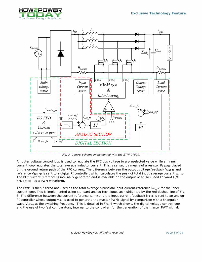
The measurement block uses 10-bit analog-to-digital converters (ADCs) with up to eight configurable channels.
This block is used for the acquisition of the feedback signals necessary for the implementation of the control scheme shown in Fig. 3.
Fig. 4. Detail of the generation of the PWM0 master signal for interleaved PFC control.
The outputs of the two comparators, COMP2 and COMP3, are sent to the driving and interleaving block where the three PWM signals used to control the three power switches are generated.
The interleaving operation is highlighted in Fig. 5. The master signal (PWM0) rising and falling edges are used
to determine the phase shift and the duty cycle of each of the two slave signals by means of two event-driven state machines embedded in the STNRGPF01 (SMED1 and SMED2 for PWM1 and SMED4 and SMED5 for PWM2).
The output of the SMEDs are SET & RESET signals processed by two flip-flops in order to generate the PWMs
signals for the two slave channels. The phase delay of the slave signals is determined by synchronizing the SMEDs with a timer counter managed by the CPU and triggered by PWM0.
The digital section, highlighted in Fig. 3 by the green dashed line, is also used for input voltage and load feed-
forward functions. When the mains voltage changes suddenly or a load current step occurs a fast transient
response is present. Finally, the programming block has I2C and UART interface, which can also be used for monitoring and communication functions.
Designing The Current-Control Loop
The interleaved boost converter small-signal transfer functions are obtained using the state-space averaging (SSA) method and a linearization operation (Taylor’s series around an operating point). It is useful in order to
calculate the PI regulators’ parameters and satisfy bandwidth and phase margin stability requirements. For the
sake of simplicity it was assumed that:
1) The converter works in CCM mode only.
2) Active and passive components are ideal.
3) The parallel boost inductors are identical and the total power is shared symmetrically in the three channels.
4) The perturbations on the mains voltage are neglected and this is assumed to be constant during several switching cycles.
In the following equations the notation “~” indicates small-signal variables while the uppercase letters refer to
steady-state operating point variables. The control-to-input current transfer function is shown in equation 1.
From this it is clear that the control-to-input current transfer function depends on the number of channels and
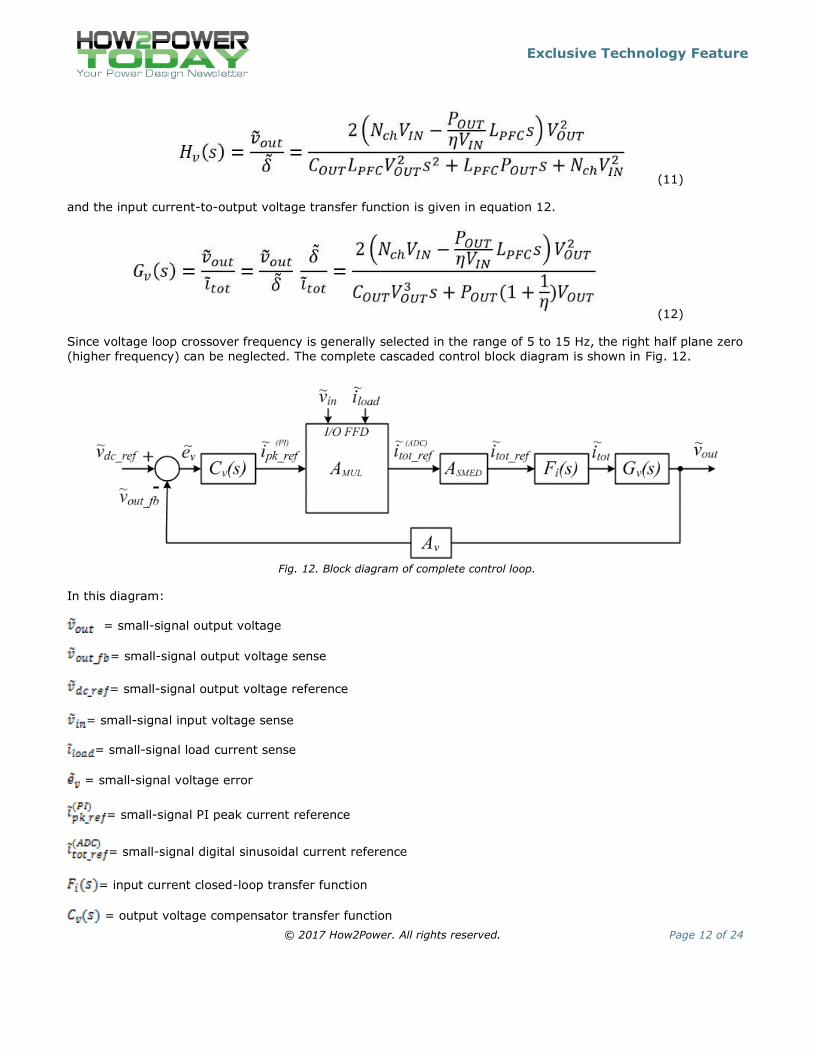
input voltage value for a fixed output power and regulated output voltage value. In the high-frequency region the following approximation can be used to simplify equation 1.
(2)
Figs. 6 and 7 show the Bode diagrams of the control-to-input current transfer function for different values of the
input voltage and number Nch of active channels respectively.
-20
0
20
40
60
80
Ma
gn
itu
de
(d
B)
10-1
100
101
102
103
104
-135
-90
-45
0
45
90
Ph
ase
(d
eg
)
Gi(s) vs V
IN
Frequency (Hz)
VIN
=90V
VIN
=115V
VIN
=140V
VIN
=185V
VIN
=230V
VIN
=265V
Fig. 6. Bode diagram of control-to-input current transfer function for different values of input
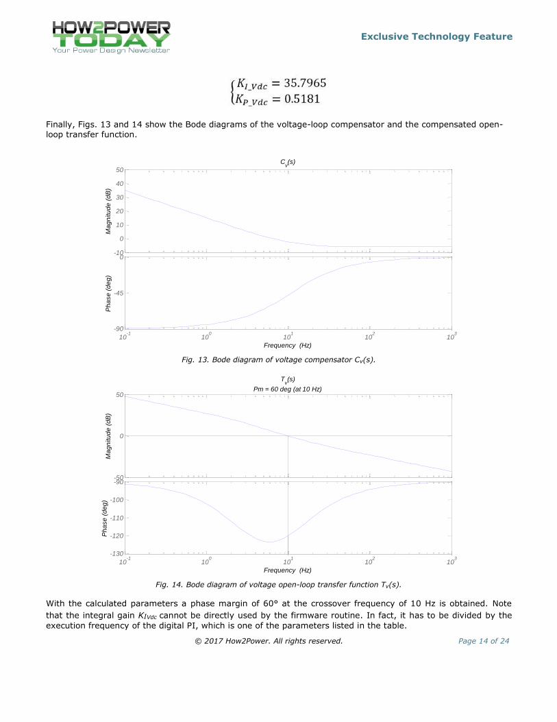
Based on these parameters and the previous guidelines for the placement of the poles and zero, the type-2 compensator amplifier parameters can be calculated as follows.
Starting from the selection of Ri, a 5.6-kΩ resistor is used. The value of Rf is then calculated so that the error
amplifier brings the control-to-input current transfer function to 0 dB at the desired closed-loop crossover frequency. Looking at the Bode plot in Fig. 7 the required gain of the error amplifier is given by:
(9)
Hence the value of Rf is calculated as
A 2.4-kΩ resistor can be used.
The high-frequency pole capacitor is calculated from equation 10.
(10)
and a 1-nF capacitor is selected for the implementation.
Lastly, using equations 6 and 8 the value the value of Cfz can be calculated as:
A 15-nF capacitor is then used.
The Bode plot of the current compensator amplifier is shown in Fig. 10 while the plot of the current open loop
where the A-D converter gain is taken into account as
(23)
This current reference is available as a PWM signal on pin 19 of the device so it has to be filtered by a proper
analog circuit in order to be used as the reference of the current control loop.
Experimental Results
The described control concept was used to implement a 3-kW three-channel interleaved boost converter. The
following specifications were used for this prototype:
Input voltage range, VIN = 90 to 265 Vac
Line frequency range, f = 47 to 63 Hz
Output power, POUT = 3 kW (1.5 kW at 115 V)
Output voltage, VOUT = 400 V
Switching Frequency, fsw = 111 kHz
Cycle-by-cycle regulation
Input voltage and load feed-forwards
Phase shedding function
Number of interleaved channels, Nch = 3.
A picture of the 3-kW three-channel interleaved PFC is shown in Fig. 16. The implementation achieves a power
density of 52 W/in3 thanks to a compact layout and the small size of the magnetic components, which are a consequence of the interleaving effect and switching frequency selection.
Fig. 16. Implementation of a 3-kW three-channel interleaved PFC.
The STNRGPF01 controller is placed on the vertically mounted PCB. The connector on the upper left hand side of this board is used to program the controller. The programming and customization of the controller functions can
be done by using a dedicate software tool called E-design suite.[5]
The design parameters reported above can be used as inputs to the software together with other specific parameters (mainly the ones reported in the table above) such as current and voltage control-loop bandwidth.
In this way a complete design is automatically generated including a schematic and bill of materials. The design
of both the analog and digital controllers discussed in the previous sections of this article are provided as well.
Most importantly, a binary code customized for the application input parameters is generated. This binary code
can be downloaded into the STNRGPF01 through the programming port. By doing so, there is no need to write
and debug complex code and the development time is dramatically reduced.
The main waveforms of the converter operating at full load in steady-state conditions when supplied from a
115-Vac source are shown in Fig. 17.
Fig. 17. Main converter waveforms in steady state.
The interleaving effect on the currents is clear. The PFC operates in CCM condition having 120° of phase shift
between the phases. The master PWM signal is shown by the yellow trace and has a duty cycle of about 60%.
The dynamic response of the converter can be appreciated in Fig. 18. The PFC is initially unloaded with the dc
bus voltage regulated at 430 Vdc with burst-mode control. As soon as a 2-kW load is applied, the output
voltage is quickly regulated at the reference value corresponding to 400 V. The initial undershoot is effectively reduced by the load feed forward action triggered by the load step.
Fig. 20 shows a similar transient response when the 2-kW load is suddenly applied while the converter is not operating in burst mode as a 400-W load is already supplied. A 10% to 100% (and 100% to 10%) load
transition is highlighted in Fig. 21. The PFC is supplied directly from the ac grid at 230 Vac. The dynamic
response is fast and the dc bus voltage is tightly regulated at the reference value.
Fig. 20. Transient response, from 0.4 kW to 2 kW to 0.4 kW.
Fig. 21. A 10% to 100% load transition with 230-Vac input; load current (blue), input current
The line voltage and current measurements are shown in the next two figures for the case where input is 115 Vac and a 1.5-kW load is applied (Fig. 22) and where input is 230 Vac and the nominal rated power is drawn
(Fig. 23). An almost unity power factor is achieved in both cases. The current is almost perfectly in phase with
the line voltage and has a very low harmonic distortion both at low input voltage and high input voltage.
Fig. 22. PFC input voltage and current at 1.5 kW with 115-Vac input.
Fig. 23. PFC input voltage and current at 3 kW with 230-Vac input.
Note that in Fig. 23 the input ac voltage includes some harmonic distortions. Even so, given the fast dynamic response of the proposed control scheme, the line current follows the reference current without distortion and
delay. In both of the cases illustrated in Figs. 22 and 23 the zero crossing distortion is minimal.
Fig. 24 shows that the current THD is well below 10% both at 115 Vac and 230 Vac even if the load is as low as 20% of the nominal value. At full power the THD is below 3% if the PFC is supplied at 115 Vac and it is equal to
3% at 230 Vac and full power. The power factor is shown in Fig. 25 as a function of the output load, with values
higher than 0.99 at low power.
The measured efficiency is shown in Fig. 26. The phase shedding control strategy results in a flat efficiency
curve, ideal to meet the most stringent requirement of new standards and regulations.
The precise Voltech PM6000 digital power meter was used to measure the PF and THD of the line current as well as the efficiency of the PFC. The maximum power that the converter can manage is de-rated at 115 Vac input
for thermal reasons.
Fig. 24. Current THD% at 115 Vac (blue) and 230 Vac (purple).
A new device called the STNRGPF01, which is suitable for CCM interleaved boost PFC converters, was presented
in this article. This device implements a semi-digital control scheme to combine the advantages of analog cycle-
by-cycle regulation with the flexibility of a digital system.
In explaining this control scheme, the design of both the analog and the digital sections, which control the input
current and output voltage regulation, respectively, were discussed and a step-by-step procedure was provided
that the power supply designer can use to determine the main parameters necessary for the implementation of these control functions. This procedure is also used in a configuration software called E-design and intended to
help the designer in achieving quick prototyping and configuration of the chip.
An evaluation board was realized in order to test the STNRGPF01 and verify the achievable performance of a 3-
kW three-channel interleaved PFC. The test results show very good performance in terms of efficiency, PF and current THD. The measured efficiency at 230 Vac was about 99% (from 40% to full load). The achieved current
THD was 3% (lower than 3% at low line, 1.5 kW) and the PF was higher than 0.99 for an output power higher
than 20% of nominal.
References
1. “Designing a high power factor switching pre-regulator with the L4981 continuous mode,”
STMicroelectronics application note AN628.
2. “STNRGPF01 Three-channel interleaved CCM PFC digital controller,” STMicroelectronics datasheet
DS10246.
3. “Designing a CCM PFC pre-regulator based on the L4984D,” STMicroelectronics application note AN4149.
4. “STNRGPF01 digital controller for interleaved PFC,” STMicroelectronics reference manual RM0446.
Rosario Attanasio is an application engineering manager at STMicroelectronics for the
Americas region, focusing on offline power supplies, industrial and lighting applications. Prior
to covering this position he served as a senior application engineer at STMicroelectronics, Italy. Rosario graduated from University of Catania in 2003 and received a PhD in electrical
engineering from the same university in 2006.
Giuseppe Di Caro is a computer science engineer. In 1982 he joined to STMicroelectronics in
Catania, where for 20 years he worked as system administrator of UNIX networks. His current activity is firmware development for advanced power electronics systems with digital control.
Sebastiano Messina received the degree in electrical engineering from the University of Catania, Italy, in 1996. From 1996 to 2001 he worked as designer engineer developing high-
voltage power systems. In 2001 he joined STMicroelectronics in Catania, Italy. Since then, he
has been working as field application engineer for lighting and power electronics systems. His current activity includes product definition for high power converters and research of new
control architectures for power conversion systems.
Marco Torrisi received the M.S. degree cum laude in electrical engineering in 2014 from the
University of Catania. In 2001 he worked at CePTIT Lab for University of Catania mainly
focusing on control algorithms for grid connected power systems. Since 2015 he has been working as application development engineer with main focus on advanced power converters.
For further reading on power factor correction in power supply applications, see the How2Power Design Guide,
select the Advanced Search option and select “Power Factor Correction” in the Popular Topics category.