Executing Simulink models on FPGA in a LabVIEW environment Master of Science Thesis in Integrated Electronic System Design OLOF KINDGREN Department of Computer Science and Engineering CHALMERS UNIVERSITY OF TECHNOLOGY UNIVERSITY OF GOTHENBURG Göteborg, Sweden, September 2009
Transcript
Executing Simulink models on FPGAin a LabVIEW environmentMaster of Science Thesis in Integrated Electronic System Design
OLOF KINDGREN
Department of Computer Science and EngineeringCHALMERS UNIVERSITY OF TECHNOLOGYUNIVERSITY OF GOTHENBURGGöteborg, Sweden, September 2009
The Author grants to Chalmers University of Technology and University of Gothenburg the non-exclusive right to publish the Work electronically and in a non-commercial purpose make it accessible on the Internet. The Author warrants that he/she is the author to the Work, and warrants that the Work does not contain text, pictures or other material that violates copyright law.
The Author shall, when transferring the rights of the Work to a third party (for example a publisher or a company), acknowledge the third party about this agreement. If the Author has signed a copyright agreement with a third party regarding the Work, the Author warrants hereby that he/she has obtained any necessary permission from this third party to let Chalmers University of Technology and University of Gothenburg store the Work electronically and make it accessible on the Internet.
Executing Simulink models on FPGA in a LabVIEW environment
Department of Computer Science and EngineeringChalmers University of TechnologySE-412 96 GöteborgSwedenTelephone + 46 (0)31-772 1000
Department of Computer Science and EngineeringGöteborg, Sweden September 2009
Abstract
This paper describes the tools, methods and problems of converting Simulinkmodels to IP blocks for FPGA and run them in the LabVIEW FPGA environ-ment. The conversion from Simulink models is performed with MathworksSimulink HDL Coder, Xilinx System Generator and by manually writingHDL code to investigate the different aspects of the workflow.
A proof-of-concept model is implemented with different parts convertedwith different methods. The analysis show that the automatic tools are usefulfor quickly implementing and verifiying DSP models. It is also noticed thatthe tools in many cases produce suboptimal code and in these cases hand-written code is the only option. The target platform, National InstrumentscompactRIO, is considered useful as there are high-level communication read-ily available, simplifying the integration with other components. The biggestproblem with the RIO platforms is the lack of control a developer has, oncethe IP is inserted in the LabVIEW FPGA design flow.
Traditionally there have been different design flows for developing systemsfor hardware and software. This forces the system designer to decide whereto deploy the different parts of a system and define an interface betweenthem early in the development process. Later on, these choices can turnout to produce a suboptimal solution. When the need arises to refactor asystem between the different platforms, it has to be reimplemented for thenew platform, using the old system as a reference. As the two platformsrequire different tool chains, design methodologies and engineering skills, alot of manual development and verification might be needed. Lately therehave been attempts to overcome this problem. The RIO[2] platforms fromNational Instrumens tries to bridge the gap between software and FPGAdevelopment by providing hardware units with FPGA, I/O, and a processorrunning a realtime OS. FPGA development for these platforms is incorpo-rated in the LabVIEW design flow and high-level communication protocolsbetween the components allow easier refactoring of a system between FPGA,realtime OS and a PC. External IP blocks can be integrated on the FPGA,allowing access to existing systems developed for FPGA.
One class of such systems especially well suited for FPGA is DSP appli-cations. For developing DSP applications in software, Simulink is often used.Simulink is a data flow programming tool with a large number of functionblocks and an environment for simulation and verification. The advantages ofusing high-level data flow programming to build DSP systems for FPGA hasbeen recognized and several tools have been created to aid in the transitionto FPGA.
The purpose of this master thesis is to examine some of the tools, meth-ods and potential problems of converting existing Simulink models writtenfor execution in software to HDL code, for implementation in the LabVIEWFPGA environment. The idea is to combine and benefit from the high speedand low latency of FPGA, the consistent programming environment of Lab-VIEW and the widespread use of Simulink models.
In Section 2 the proposed workflow is presented, together with a fewalternative methods, when applicable. Section 3 describes a model that hasbeen implemented as a proof-of-concept. This model, along with generalobservations is analyzed in Section 4 and a summarized conclusion is foundin Section 5, together with notes of what was left out in the writing of thisthesis.
Figure 1 on page 5 shows an overview of the different formats that canbe used and how to translate between them.
4
VI VI VI
XML CLIP NGC
FPGAdesigner VHDL
XST/Synplify
SystemGenerator
SimulinkHDL coder Simulink FPGA
designer
LabVIEW FPGA LabVIEW RT LabVIEW Windows
User
File format
Tool
Data flow
Tool chain
Figure 1: Toolchain overview
2 Workflow
Integrating a Simulink model written for execution in software into the Lab-VIEW FPGA environment requires several intermediate steps, and can bedone in different ways with different tools. The ultimate goal, however is tohave a net list or synthesisable HDL code which is functionally equivalent tothe original Simulink model and can be imported into LabVIEW.
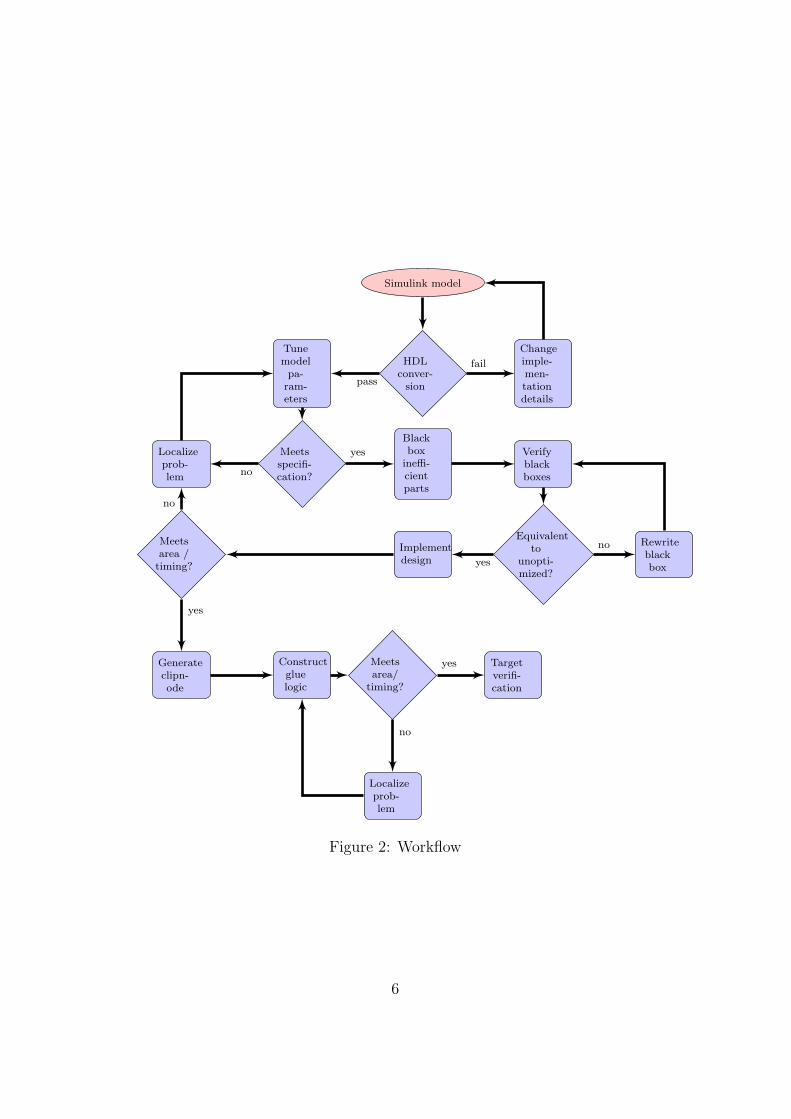
Every modification that occur to the model during the conversion mayhave an impact on function, chip area, precision and speed. It is thereforeimportant to be able to verify the correctness of the model at all stages inthe conversion. In some cases this can be done by testing for equivalencewith the previous iteration. When changes to the model has to be made in away that no longer makes it equivalent to the previous iteration, the modelshould instead be checked against the original specifications. An outline ofthe workflow is summarized in Figure 2 on page 6.
2.1 Preparing the model
Only a subset of the function blocks and features in Simulink can be real-ized in FPGA. Therefore the first step to make the model ready for HDLgeneration is to identify incompatibilities. This includes:
• Using a fixed-step discrete time solver instead of continuous states toemulate clocked logic design.
5
Simulink model
HDLconver-
sion
Changeimple-men-tationdetails
Tunemodel
pa-ram-eters
Meetsspecifi-cation?
Localizeprob-lem
Blackbox
ineffi-cientparts
Verifyblackboxes
Equivalentto
unopti-mized?
Rewriteblackbox
Implementdesign
Meetsarea /
timing?
Generateclipn-ode
Constructgluelogic
Meetsarea/
timing?
Localizeprob-lem
Targetverifi-cation
fail
pass
no
yes
no
yes
yes
no
no
yes
Figure 2: Workflow
6
• Replacing all floating point arithmetics with fixed-point.
• Only use blocks for which there exists a corresponding HDL implemen-tation.
The model may not be able to directly use a fixed-step discrete time solver,which is a prerequisite for converting the model. In some cases models mayneed to undergo too drastic changes to be candidates for implementation inFPGA, while others can be used after some redesign.
The use of fixed-point arithmetics instead of floating point will in mostcases introduce some precision loss. The amount of precision loss is relatedto the size of the fixed-point signal paths and the method used to roundfixed-point numbers. This is a trade-off between silicon area and precisionand must be taken into consideration.
Simulink HDL Coder maintains a list of blocks that have a HDL imple-mentation, and any model can be checked against this list. The number ofsupported blocks increase for every version of Simulink HDL Coder, and atthe time of writing, the list included most arithmetic operations, tools forfilter design and support writing embedded M Code. Some blocks, such asgraphical output or file I/O, have no equivalent implementation in FPGAand are therefore excluded. Other native Simulink blocks may not yet beported and must therefore be built from more primitive blocks.
2.2 Generating HDL code
Starting out from a Simulink model there are three proposed ways to turnthis into HDL. The whole model can be implemented using one method ordifferent methods can be used for subsets of the model. The three methodsanalyzed here are:
• Convert with Simulink HDL coderMathworks Simulink HDL Coder[3] is a tool for converting a modelbuilt in Simulink directly to VHDL or Verilog, and is aimed at rapidprototyping. All native Simulink blocks however are not supported bySimulink HDL Coder and the model must therefore be built using thesupported subset of blocks. To automate the process Simulink HDLCoder can analyze a model and inform the designer of what needs tobe done. If all criterias are met, the model can be translated to HDL.If changes were made to the model it should be compared with theoriginal model by cosimulating them inside of Simulink. In addition tothe generated code, Simulink HDL Coder can also provide test benches
7
with stimuli to aid in the HDL verification process. Using SimulinkHDL Coder is assumed to be the preferred way of generating HDLcode in this report, since it requires the least effort when dealing withexisting Simulink models. The other methods are primarily used ascomplements when using Simulink HDL coder is not applicable.
• Build an equivalent Xilinx System Generator modelXilinx System Generator[8] provides a library of Simulink blocks thatare designed for implementation in Xilinx FPGA. Using only theseblocks, Xilinx System Generator can synthezise the model into netlistswith an optional HDL wrapper. The blocks on the Simulink blockdiagram are mostly implemented as Xilinx IP blocks, such as thoseavailable from Xilinx Core Generator. Xiling System Generator alsogenerates a large amount of VHDL macro functions to handle dataconversion between the blocks. As only System Generator blocks aresupported in this workflow, a Simulink model must be manually con-verted from using native Simulink blocks. For verification of modelcorrectness, the two models can be cosimulated inside of Simulink tocheck for equivalence.
• Write equivalent HDL codeBy analyzing the behaviour of the model, HDL code representing anequivalent model can be written manually. In order to test the equiv-alence of the HDL implementation with the Simulink model, SimulinkHDL Coder can provide test benches for ModelSim and a few otherlogic simulators. These test benches contain pregenerated input andoutput vectors based on the original model to be used as stimuli. Thisis meant as a last resort, as the emphasis of this paper is on automatedconversion methods.
2.3 Optimizing HDL code
Even if the generated HDL code can be synthezised and meets the specifi-cations, the design might be suboptimal for FPGA implementation. Manyof the default implementations of the Simulink blocks are optimized for lowlatency, to mimic their software equivalents, which generally have no latency.This can however have a negative impact on speed and area when a FPGA isthe target. A test build of the generated code is therefore needed to ensurethat the code meets these requirements.
Should the code not satisfy the demands for area and speed the problemshould be localized. There are then several ways of improving the code, while
8
still taking advantage of the automatically generated test benches and theSimulink environment.
2.3.1 Tuning the model
Many arithmetic blocks grow linearly or even exponentially depending on thesize of the bus width of the input and output data. For a DSP applicationthere can be much to gain by minimizing the needed bus width in the signalchain, as a too wide bus will use up excessive resources without adding anybenefit. Narrowing down the bus too much will have a negative impact onSNR1 due to rounding errors, and can also effect the functional requirementson the design. The SNR can often be related to the bit width as 6dB perextra bit[6].
A different approach is to completely change the implementation of someblock. Complex blocks generally have more options to choose from, but evena simple function such as an adder can have several implementations, eachfocused on small area, high clock speed or low latency. There are also moregeneric parameters to take into consideration, such as providing synchronous,asynchronous or no reset at all to a block.
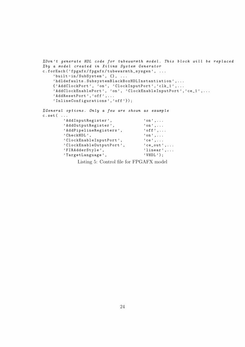
Simulink HDL coder provides a way to specify these parameters in a con-trol file, which is consulted when the HDL code is generated. The parameterscan be set for individual blocks, classes of blocks or whole subsystems. Partsof a commented control file is included in Listing 5 on page 23. Using SystemGenerator these parameters are instead specified directly in the blocks used.
2.3.2 Black-boxing
If changing bit widths or tweaking model parameters won’t give the desiredresults, or if there is no feasible way to implement a part of the designwith Simulink HDL Coder or System Generator, that part of the model canbe black-boxed. Black-boxing a subset of a model prevents the tool fromgenerating HDL code for that part. Instead it can be replaced with a netlistor external HDL code which is compiled with the rest of the model aftersynthesis. The black box can still contain a Simulink model which is usedfor simulating the behaviour inside of Simulink.
1Signal to Noise Ratio. Defines the amplitude of a signal compared to the backgroundnoise
9
2.4 Integrating with LabVIEW
The LabVIEW software environment is a dataflow programming languagefor software development for many targets, including Mac and PC as wellas several embedded platforms. The user interface together with a blockdiagram containing functional code is called a VI (Virtual Instrument), asit originally was made to emulate desktop instruments such as oscilloscopesand signal generators.
This concept has also been expanded to generate FPGA load files forthe RIO platforms from a block diagram. The RIO platforms are a seriesof hardware units from National Instruments containing a FPGA and I/O.Several of these systems also contain a CPU running a realtime OS andonboard memory, effectively turning it into an embedded computer with adedicated FPGA for I/O handling.
The generated load file contains the code generated from the block di-agram and a wrapper which LabVIEW uses internally to handle all FPGAI/O. The I/O consist both of communication with the host system for theFPGA, and any I/O modules that may be present on the selected platform.This prevents the developer from having direct access to the I/O, and insteadrelying on higher-level LabVIEW defined communication protocols. The in-tention of this is to reduce the amount of custom protocols and glue logicthat needs to be written.
When building a block diagram, the developer has access to many Lab-VIEW function blocks, such as integer and fixed-point arithmetics, signalgeneration and analysis tools and many of the built-in dataflow design pat-terns. In addition to the built-in function blocks, there is also a system calledCLIP[5] to include external IP blocks. CLIP allows developers to access thetop-level entity of a IP block as if it was a built-in function block. To inserta CLIP into a LabVIEW project an XML description file is used to provideinformation about the IP to LabVIEW. The XML file describes the following:
• Connection between HDL entity names and LabVIEW signal names
• Which HDL entity signals that should be used for clock and reset.
• The frequency the CLIP should be compiled for
• Files that should be included when building the CLIP
• Name of the top entity
Clock and reset signals are handled transparently in LabVIEW. All othersignals are passed to the VI and can be used to connect the CLIP to other
10
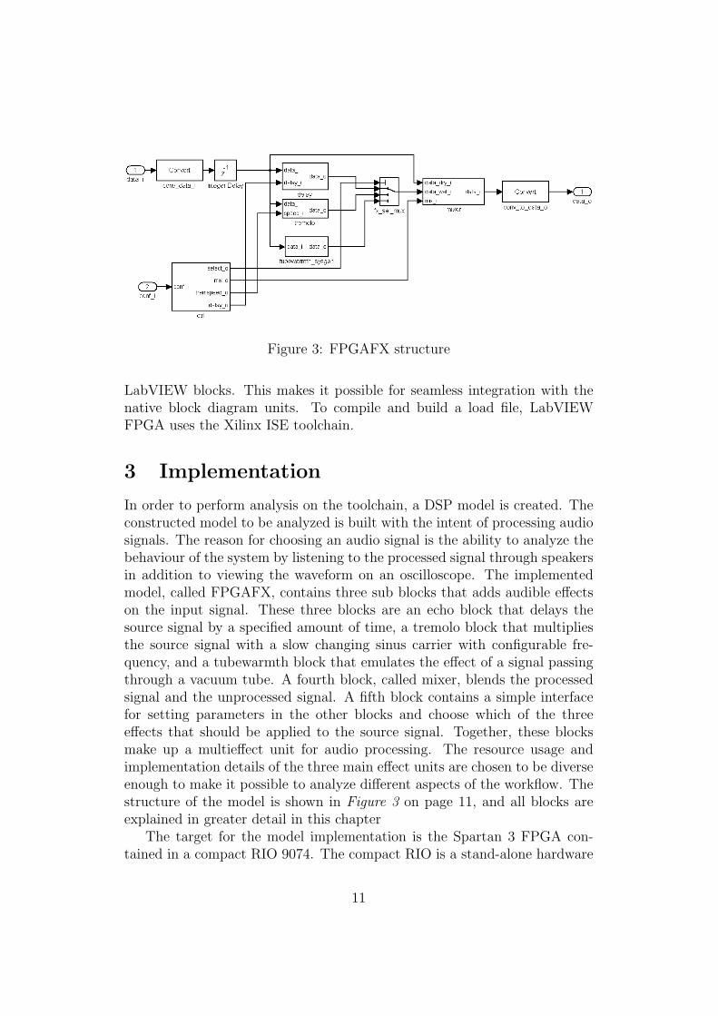
Figure 3: FPGAFX structure
LabVIEW blocks. This makes it possible for seamless integration with thenative block diagram units. To compile and build a load file, LabVIEWFPGA uses the Xilinx ISE toolchain.
3 Implementation
In order to perform analysis on the toolchain, a DSP model is created. Theconstructed model to be analyzed is built with the intent of processing audiosignals. The reason for choosing an audio signal is the ability to analyze thebehaviour of the system by listening to the processed signal through speakersin addition to viewing the waveform on an oscilloscope. The implementedmodel, called FPGAFX, contains three sub blocks that adds audible effectson the input signal. These three blocks are an echo block that delays thesource signal by a specified amount of time, a tremolo block that multipliesthe source signal with a slow changing sinus carrier with configurable fre-quency, and a tubewarmth block that emulates the effect of a signal passingthrough a vacuum tube. A fourth block, called mixer, blends the processedsignal and the unprocessed signal. A fifth block contains a simple interfacefor setting parameters in the other blocks and choose which of the threeeffects that should be applied to the source signal. Together, these blocksmake up a multieffect unit for audio processing. The resource usage andimplementation details of the three main effect units are chosen to be diverseenough to make it possible to analyze different aspects of the workflow. Thestructure of the model is shown in Figure 3 on page 11, and all blocks areexplained in greater detail in this chapter
The target for the model implementation is the Spartan 3 FPGA con-tained in a compact RIO 9074. The compact RIO is a stand-alone hardware
11
Figure 4: Compact RIO overview
unit with a FPGA situated between pluggable IO modules and a 400MHzPPC CPU running a real-time OS. The I/O modules used in this setup con-sists of a NI cRIO-9215 A/D converter and a NI 9263 D/A converter. TheCPU runs a VxWorks OS with an application to monitor and control theFPGA. The load file for the FPGA consists of both HDL code generatedfrom LabVIEW block diagrams and external HDL code imported as a CLIP,that make up the user defined parts of the FPGA. During the building of theload file, LabVIEW also inserts code for I/O handling, as seen in Figure 4on page 12
3.1 Test environment
As seen in Figure 5 on page 13, the model recieves its input from an analogsource via a NI cRIO-9215 A/D converter. The processed signal is sent to aPC over ethernet or directly to a NI 9263 D/A converter.
The FPGA uses the fsys = 40MHz onboard clock available on the com-pact RIO platform, and a common sampling rate, which is a fraction of fsys
for the A/D and the D/A converters. As audio is the intended input, a sam-pling rate of fsys/1814 ≈ 22050Hz is used for the system. The word lengthof the system is 16 bits.
The model under analysis is packaged as a CLIP called FPGAFX andis placed between FIFOs to provide protection from jitter in communicationboth with the I/O module and the CPU.
The analog output is connected to an oscilloscope and a speaker to provideboth visual and audible feedback.
Configuration of the FPGA parameters are controlled from the CPU onthe compact RIO.
12
A/D FIFO FPGAFX FIFO
FIFO
CPU
D/A
PC Sound card
Figure 5: Test environment
X
X
+-
sdry
mixmaxmix
swet
sout
Figure 6: Mixer
3.2 Mixer
The purpose of the mixer is to mix two audio sources, in this case the un-processed (dry) signal with the processed (wet) signal. Assuming the mixsignal has a range [0 : mixmax[ the mixed output signal can be described assout = swet ·mix + sdry · (mixmax −mix).
For the fixed-point implementation mix is implemented as a 8-bit un-signed number without a decimal part, and therefore mixmax = 1. Usingmod((2n−1)−mix, 2n) = mod(2n−1+mix+1, 2n) = mix the equation canbe simplified to sout = swet ·mix + sdry ·mix). The original implementationis shown in Figure 6 on page 13
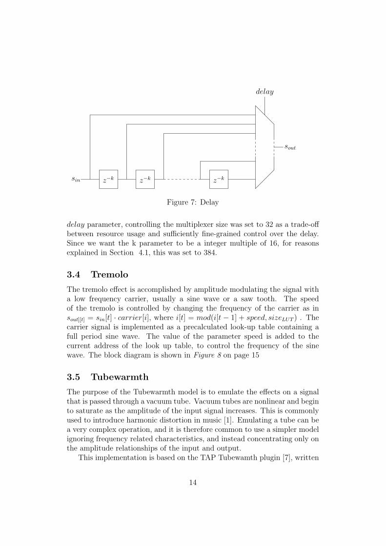
3.3 Delay
The delay model shown in Figure 7 on page 14 is implemented as a chainof delay elements, each delaying the signal k cycles. The signal is tappedoff between every shift register, and a multiplexer selects which tap to out-put, thereby controlling the delay time. The algorithm can be described assout[t] = sin[t− k · delay · Ts].
The maximum delay time is limited by the available FPGA resources thatcan be used for the delay chain, and was found to be around 12000 elements,resulting in a maximum delay of ≈ 0.5s for the given sampling rate. The
13
z−k z−k z−ksin
sout
delay
Figure 7: Delay
delay parameter, controlling the multiplexer size was set to 32 as a trade-offbetween resource usage and sufficiently fine-grained control over the delay.Since we want the k parameter to be a integer multiple of 16, for reasonsexplained in Section 4.1, this was set to 384.
3.4 Tremolo
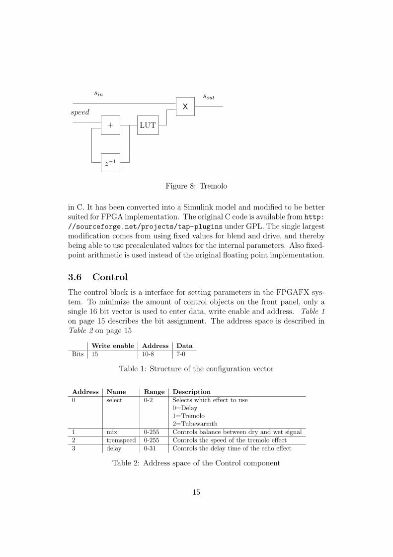
The tremolo effect is accomplished by amplitude modulating the signal witha low frequency carrier, usually a sine wave or a saw tooth. The speedof the tremolo is controlled by changing the frequency of the carrier as insout][t] = sin[t] · carrier[i], where i[t] = mod(i[t − 1] + speed, sizeLUT ) . Thecarrier signal is implemented as a precalculated look-up table containing afull period sine wave. The value of the parameter speed is added to thecurrent address of the look up table, to control the frequency of the sinewave. The block diagram is shown in Figure 8 on page 15
3.5 Tubewarmth
The purpose of the Tubewarmth model is to emulate the effects on a signalthat is passed through a vacuum tube. Vacuum tubes are nonlinear and beginto saturate as the amplitude of the input signal increases. This is commonlyused to introduce harmonic distortion in music [1]. Emulating a tube can bea very complex operation, and it is therefore common to use a simpler modelignoring frequency related characteristics, and instead concentrating only onthe amplitude relationships of the input and output.
This implementation is based on the TAP Tubewamth plugin [7], written
14
z−1
+ LUT
X
sin
speed
sout
Figure 8: Tremolo
in C. It has been converted into a Simulink model and modified to be bettersuited for FPGA implementation. The original C code is available from http:
//sourceforge.net/projects/tap-plugins under GPL. The single largestmodification comes from using fixed values for blend and drive, and therebybeing able to use precalculated values for the internal parameters. Also fixed-point arithmetic is used instead of the original floating point implementation.
3.6 Control
The control block is a interface for setting parameters in the FPGAFX sys-tem. To minimize the amount of control objects on the front panel, only asingle 16 bit vector is used to enter data, write enable and address. Table 1on page 15 describes the bit assignment. The address space is described inTable 2 on page 15
Write enable Address DataBits 15 10-8 7-0
Table 1: Structure of the configuration vector
Address Name Range Description0 select 0-2 Selects which effect to use
0=Delay1=Tremolo2=Tubewarmth
1 mix 0-255 Controls balance between dry and wet signal2 tremspeed 0-255 Controls the speed of the tremolo effect3 delay 0-31 Controls the delay time of the echo effect
During the conversion of FPGAFX several complications were brought toattention. Some of these were solved by a slight modification of the model,or by changing implementation parameters. Others prevented the conversionfrom being executed automatically and required manual intervention to solve.This section describes the specific problems and solutions for the FPGAFXmodel, giving a context for some of the general problems that can arise inthe conversion process.
4.1 Delay
The delay model consists primarly of memory capable elements. The numberof elements grow linearly with the length and width of the delay chain. Asthere are several different types of memory capable elements in an FPGA,such as RAM, flip-flops and shift registers, different implementations canproduce vastly different results regarding resorce usage.
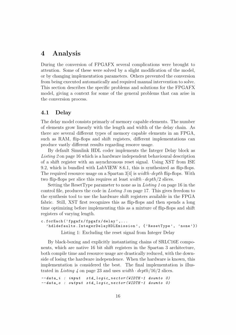
By default Simulink HDL coder implements the Integer Delay block asListing 2 on page 16 which is a hardware independent behavioural descriptionof a shift register with an asynchronous reset signal. Using XST from ISE9.2, which is bundled with LabVIEW 8.6.1, this is synthesized as flip-flops.The required resource usage on a Spartan 3[4] is width·depth flip-flops. Withtwo flip-flops per slice this requires at least width · depth/2 slices.
Setting the ResetType parameter to none as in Listing 1 on page 16 in thecontrol file, produces the code in Listing 3 on page 17. This gives freedom tothe synthesis tool to use the hardware shift registers available in the FPGAfabric. Still, XST first recognizes this as flip-flops and then spends a longtime optimizing before implementing this as a mixture of flip-flops and shiftregisters of varying length.
Listing 1: Excluding the reset signal from Integer Delay
By black-boxing and explicitly instantiating chains of SRLC16E compo-nents, which are native 16 bit shift registers in the Spartan 3 architecture,both compile time and resource usage are drastically reduced, with the down-side of losing the hardware independence. When the hardware is known, thisimplementation is considered the best. The final implementation is illus-trated in Listing 4 on page 23 and uses width · depth/16/2 slices.
--data : signal array(0 to DEPTH -1) of std_logic_vector(WIDTH -1 downto 0)
process (clk ,rst)begin
if rising_edge(clk) thenif ce = ’1’ then
data <= data(DEPTH -2 downto 0) & data_i;end if;
end if;end process;data_o <= data(DEPTH -1);
Listing 3: Behavioral description of a shift-register without reset
The resource usage of the different cases is summarized in Table 3 onpage 17
Available SRLC16E Default No resetNumber of Slices 20480 7700 35457 17200Number of Slice Flip Flops 40960 20 55153 23275Number of 4 input LUTs 40960 15358 30434 28868
Table 3: Resource usage of the delay block with different implementations
4.2 Tremolo
When implementing the Tremolo block in Simulink HDL Coder, the originalidea was to use the built-in Sine lookup table, which takes advantage ofquarter-wave symmetry. This was not possible due to a flaw in the HDLgeneration that prevented a signed and an unsigned number in the internalrepresentation of the Sine lookup table block. Instead an ordinary lookup
17
table was used. In this case this was not a problem since the differences inresource usage was relatively small. This, however, highlights some of theunexpected problems that one can come across, and have to work around, inthe conversion stage.
4.3 Tubewarmth
The tubewarmth model uses several arithmetic functions such as multipliers,adders and a square root. The square root especially has several alternativeimplementations that vary in area, speed, accuracy and latency.
Using the tubewarmth block created from the Simulink HDL coder modelwas not possible to do on the Spartan 3 FPGA, due to insufficient resources.Aside from using a large amount of the available logic, the tubewarmth blockuses all available 18x18 multipliers, leaving no resources to the LabVIEWgenerated HDL code.
As a first attempt to solve this, the logic for generating the internal pa-rameters was replaced with precalculated constants. Also, the internal signalpaths were made as narrow as possible without losing noticable audio qual-ity. Investigation of the RTL schematics and build logs revealed that thesquare root blocks was responsible for the largest part of the resource usage.Simulink HDL coder uses the multiply/add algorithm and produces combi-natorial code. This has the advantage of being the closest to a model writtenfor software, but does not incorporate well into the pipelining methodologyused in FPGA/ASIC design. It also uses a lot of chip area.
The solution to this was to black-box the Tubewarmth sub block andinstead build an equivalent model using Xilinx System Generator. Modelscreated with Xilinx System Generator is targeted at a specific FPGA, andcan therefore take advantage of the hardware resources in a more efficientway. Also, many of the implementations are based on iterative CORDICalgorithms, which can save considerable amounts of logic.
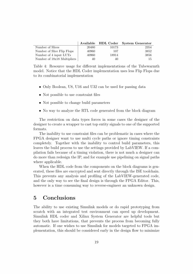
For reference, both implementations were synthesized for Spartan 3 out-side of the LabVIEW environment. The relevant resource usages are sum-marized in Table 4 on page 19
4.4 CLIP
The integration of the model as a CLIP has some limitations. Most of thelimitations are intentional to easily fit the CLIP into the LabVIEW designflow, and to hide low level FPGA behaviour.
• CLIP cannot access FPGA pins directly
18
Available HDL Coder System GeneratorNumber of Slices 20480 10173 2354Number of Slice Flip Flops 40960 107 3852Number of 4 input LUTs 40960 18914 3856Number of 18x18 Multipliers 40 40 15
Table 4: Resource usage for different implementations of the Tubewarmthmodel. Notice that the HDL Coder implementation uses less Flip Flops dueto its combinatorial implementation
• Only Boolean, U8, U16 and U32 can be used for passing data
• Not possible to use constraint files
• Not possible to change build parameters
• No way to analyze the RTL code generated from the block diagram
The restriction on data types forces in some cases the designer of thedesigner to create a wrapper to cast top entity signals to one of the supportedformats.
The inability to use constraint files can be problematic in cases where theFPGA designer want to use multi cycle paths or ignore timing constraintscompletely. Together with the inability to control build parameters, thisleaves the build process to use the settings provided by LabVIEW. If a com-pilation fails because of a timing violation, there is not much a designer cando more than redesign the IP, and for example use pipelining on signal pathswhere applicable.
When the HDL code from the components on the block diagrams is gen-erated, these files are encrypted and sent directly through the ISE toolchain.This prevents any analysis and profiling of the LabVIEW-generated code,and the only way to see the final design is through the FPGA Editor. This,however is a time consuming way to reverse-engineer an unknown design.
5 Conclusions
The ability to use existing Simulink models or do rapid prototyping fromscratch with an integrated test environment can speed up development.Simulink HDL coder and Xilinx System Generator are helpful tools butthey both have limitations, that prevents the process from becoming fullyautomatic. If one wishes to use Simulink for models targeted to FPGA im-plementation, this should be considered early in the design flow to minimize
19
manual intervention as much as possible. Still, the ability to black box someparts of the design is a necessary feature because of the limitations SimulinkHDL Coder currently contains.
With Simulink HDL Coder, implementation of many blocks fails to takeadvantage of dedicated hardware resources. In the delay model, the SRLC16Eprimitives were far from optimally utilized when synthesized with XST. Thiscould be compared with other synthesis tools such as Synopsis Synplify pro,but as there was no access to other tools this was considered to be outsidethe scope of this thesis.
Another problem with Simulink HDL Coder is the choice of block im-plementations that highlight the inherent differences between software andhardware modelling. Many designs require non-uniform step sizes whichprevent them from being used, at least directly, as a clocked design. Themodels that can use fixed step-sizes most probably contain blocks that needone or none cycles to execute, after which their state is updated to the nextiteration. An equivalent HDL implementation often produces large combi-natorial logic nets, which is badly suited for FPGA. This can be seen in theTubewarmth model where the square root block and the multipliers were solarge that they consumed five times as many LUTs as the System Generatorimplementation.
A fundemental reason for this is that Simulink HDL Coder provides nobuilt-in handshaking mechanism telling the blocks when the previous blockis done calculating and the next are ready to input data. LabVIEW FPGAand System Generator uses handshaking, which allows the blocks to consumeseveral cycles while still maintaining the data.
There were also more subtle failings of the HDL generation in SimulinkHDL Coder , such as the inability to use the sine lookup table. Limitationssuch as these hinders the workflow when working with Simulink HDL Coder.
On the other hand, Xilinx System Generator requires a manual conver-sion to the supported blocks. This means that an extra conversion step isintroduced, requiring another round of verification. But once this is done,the close integration with the rest of the Xilinx platform and the behind-the-scenes knowledge makes this a powerful tool for resource-efficient implemen-tations. The downside in this case is that it is not as easy to implement in anexisting design as Simulink HDL coder, and it is directly targeted towardsXilinx hardware.
Both tools are primarly used for DSP programming. Other types ofsystems may still be easier to implement by hand, and it is therefore a goodthing that there are ways to incorporate external HDL Code in the designflow.
Once the generated IP is in the LabVIEW FPGA environment it is easy
20
to incorporate it in the LabVIEW design flow, but there are also more po-tential problems. LabVIEW FPGA 8.6.1, which is the current version atthis time of writing, uses Xilinx ISE 9.2 as a backend for building the FPGAload file. ISE 9.2 is a worse performer than ISE 10.1, and as ISE 11 is re-cently released, it is even more dated. Also, what LabVIEW FPGA gains insimplicity, it also loses in control. There is no way to specify constraints orsetting parameters for the Xilinx tool chain. Every timing violation makesthe build process fail. Together with the inability to analyse the LabVIEWgenerated code, due to the encryption of the HDL files, this makes build-ing for a LabVIEW supported FPGA targets a trial-and-error process, whenthe limits are pushed. Still, LabVIEW FPGA is a powerful platform forrapid prototyping, and with the CLIP system, designs can easily be movedto stand-alone FPGA with a different I/O layer if needed.
The toolchain tested is very useful for implementing DSP systems fromSimulink on FPGA. The simulation and verification tools are also of greathelp, as it minimizes the amount of redundant test benches that needs to bewritten, which also mimimizes the need to verify the verification environmentmore than necessary. There are however some rough edges to this, and theability to use hand-written HDL code is still required. The toolchain will notreplace the manual work as cutting edge designs need the options to finetuneconstraints and analyze every part of the design. On the other hand, this isnot the target application. The tools are developed to give system designersand LabVIEW programmers the possibility to use FPGA in their designflow. Experienced FPGA programmers can then provide them with highperformance IP cores that are black boxed for LabVIEW.
During the writing of this paper I also learned about Synplify DSP, witha scope similar to that of System Generator and Simulink HDL Coder. Un-fortunately there was no access to the tool.
References
[1] Merlin Blencowe, Chapter 1: The common cathode, triode gain stage,http://www.freewebs.com/valvewizard1/Common_Gain_Stage.pdf.
[2] National Instruments Corporation, About RIO Technology, http://www.ni.com/fpga/rio.htm.
[3] The MathWorks Inc, Simulink HDL Coder product overview, http://
port (d : in std_logic_vector(width -1 downto 0);ce : in std_logic;clk : in std_logic;q : out std_logic_vector(width - 1 downto 0));
end srlc16e_vec;
architecture rtl of srlc16e_vec is--Declare the native 16 bit shift registers of a Spartan 3
component SRLC16Eport (
d : in std_logic;ce : in std_logic;clk : in std_logic;a0 : in std_logic;a1 : in std_logic;a2 : in std_logic;a3 : in std_logic;q : out std_logic;q15 : out std_logic );
end component;begin
--Generate a 20 bit wide Shift registers.
g_srl_w: for i in 0 to width - 1 generatei_srl : SRLC16E port map(d(i),ce,clk ,’1’,’1’,’1’,’1’,open ,q(i));
end generate g_srl_w;end rtl;
Listing 4: Hardware specific description of a shift-register
function c = fpgafx_ctrl
c = hdlnewcontrol(mfilename );
c.generateHDLFor(’fpgafx/fpgafx ’);
%Don ’t generate HDL code for delay model. This block will be replaced