Dev Bhoomi Institute Of Technology Department of Electrical and Electronics Engineering LABORATORY MANUAL PRACTICAL INSTRUCTION SHEET EXPERIMENT NO. ISSUE NO. : ISSUE DATE: 10-July-2010 REV. NO. : REV. DATE : PAGE: 1 LABORATORY Name & Code: PEE653:Power Electronics Lab SEMESTER: VI Prepared By- Mr.Shubham Chamoli Approved By- Mr. Rohit Kumar Experiment No-1 Theory and Concept Objective : To study V-I characteristics of SCR and measure latching and holding currents. APPARATUSREQUIRED: THEORY: Fig (a) Elemantry circuit for obtaining thyrsistor V-I characteristics
Transcript
Dev Bhoomi Institute Of Technology Department of Electrical and Electronics
Engineering
LABORATORY
MANUAL
PRACTICAL INSTRUCTION SHEET
EXPERIMENT NO. ISSUE NO. : ISSUE DATE:
10-July-2010
REV. NO. : REV. DATE :
PAGE: 1
LABORATORY Name & Code: PEE653:Power Electronics Lab SEMESTER: VI
Prepared By- Mr.Shubham Chamoli Approved By- Mr. Rohit Kumar
Experiment No-1
Theory and Concept Objective: To study V-I characteristics of SCR and measure latching and holding currents.
APPARATUSREQUIRED:
THEORY:
Fig (a) Elemantry circuit for obtaining thyrsistor V-I characteristics
Dev Bhoomi Institute Of Technology Department of Electrical and Electronics
Engineering
LABORATORY
MANUAL
PRACTICAL INSTRUCTION SHEET
EXPERIMENT NO. ISSUE NO. : ISSUE DATE:
10-July-2010
REV. NO. : REV. DATE :
PAGE: 2
LABORATORY Name & Code: PEE653:Power Electronics Lab SEMESTER: VI
Prepared By- Mr.Shubham Chamoli Approved By- Mr. Rohit Kumar
Fig (b) Static V-I characteristics of thyrsistor
An elementary circuit diagram for obtaining static V-I characteristics of a thyristor is shown in Fig. 4.2
(a). The anode and cathode are connected to main source through the load. The gate and cathode are fed
from a source Es which provides positive gate current from gate to cathode.
Fig. 4.2 (b) shows static V-I characteristics of a thyristor. Here Va is the anode voltage across thyristor
terminals A, K and Ia is the anode current. Typical SCR V-I characteristic
Dev Bhoomi Institute Of Technology Department of Electrical and Electronics
Engineering
LABORATORY
MANUAL
PRACTICAL INSTRUCTION SHEET
EXPERIMENT NO. ISSUE NO. : ISSUE DATE:
10-July-2010
REV. NO. : REV. DATE :
PAGE: 3
LABORATORY Name & Code: PEE653:Power Electronics Lab SEMESTER: VI
Prepared By- Mr.Shubham Chamoli Approved By- Mr. Rohit Kumar
shown in Fig. 4.2 (b) reveals that thyrsistor has three basic modes of operation; namely, reverse blocking
mode, forward blocking (off-state) mode and forward conduction (on-state) mode. These three modes of
operation are now discussed below:
Reverse Blocking Mode: When cathode is made positive with respect to anode with switch S open, Fig.
4.2 (a), thyristor is reverse biased as shown in Fig. 4.3 (a). Junctions J1 J3 are seen to be reverse biased
whereas junction J2 is forward biased. The device behaves as if two diodes are connected in series with
reverse voltage applied across them. A small leakage current of the order of a few milliamperes (or a few
microamperes depending upon the SCR rating) flows. This is reverse blocking mode, called the off-state,
of the thyristor. If the reverse voltage is increased, then at a critical breakdown level, called reverse break-
down voltage VBR, an avalanche occurs at J1 and J3 and the reverse current increases rap-idly. A large
current associated with VBR gives rise to more losses in the SCR. This may lead to thyristor damage as
the junction temperature may exceed its permissible tempera-ture rise. It should, therefore, be ensured that
maximum working reverse voltage across a thyristor does not exceed VBR. When reverse voltage applied
across a thyristor is less than VBR, the device offers a high impedance in the reverse direction. The SCR
in the reverse blocking mode may therefore be treated as an open switch.
Note that V-I characteristic after avalanche breakdown during reverse blocking mode is applicable only
when load resistance is zero, Fig. 4.2 (b). In case load resistance is present, a large anode current
associated with avalanche breakdown at VBR would cause substantial voltage drop across load and as a
result, V-I characteristic in third quadrant would bend to the right of vertical line drawn at VBR.
Forward Blocking Mode: When anode is positive with respect to the cathode, with gate circuit open,
thyristor is said to be forward biased as shown in Fig. 4.3 (b). It is seen from this figure that junctions J1,
J3 are forward biased but junction J2 is reverse biased. In this mode, a small current, called forward
leakage current, flows as shown in Figs. 4.2 (b) and 4.3 (b). In case the forward voltage is increased, then
the reverse biased junction J2 will have an avalanche breakdown at a voltage called forward break over
voltage VB0. When forward voltage is less than VBO, SCR offers high impedance. Therefore, a thyristor
can be treated as an open switch even in the forward blocking mode.
Forward Conduction Mode: In this mode, thyristor conducts currents from anode to cathode with a very
small voltage drop across it. A thyristor is brought from forward blocking mode to forward conduction
mode by turning it on by exceeding the forward breakover voltage or by applying a gate pulse between
gate and cathode. In this mode, thy-ristor is in on-state and behaves like a closed switch. Voltage drop
across thyristor in the on state is of the order of 1 to 2 V depending on the rating of SCR. It may be seen
from Fig. 4.2 (b) that this voltage drop increases slightly with an increase in anode current. In conduction
mode, anode current is limited by load impedance alone as voltage drop across SCR is quite small. This
small voltage drop v across the device is due to ohmic drop in the four layers.
Dev Bhoomi Institute Of Technology Department of Electrical and Electronics
Engineering
LABORATORY
MANUAL
PRACTICAL INSTRUCTION SHEET
EXPERIMENT NO. ISSUE NO. : ISSUE DATE:
10-July-2010
REV. NO. : REV. DATE :
PAGE: 4
LABORATORY Name & Code: PEE653:Power Electronics Lab SEMESTER: VI
Prepared By- Mr.Shubham Chamoli Approved By- Mr. Rohit Kumar
CIRCUIT DIAGRAM:
PROCEDURE:
1. Connections are made as shown in the circuit diagram.
2. The value of gate current IG, is set to convenient value by adjusting VGG.
3. By varying the anode cathode voltage VAA gradually in step by step, note down the cor-responding
values of VAK and IA . Note down VAK and IA at the instant of firing of SCR and after firing (by
reducing the voltmeter ranges and ammeter ranges) then increase the supply voltage VAA . Note down
corresponding values of VAK and IA.
4. The point at which SCR fires, gives the value of break over voltage VBO.
5. A graph of VAK V/S IA is to be plotted.
6. The on state resistance can be calculated from the graph by using a formula.
7. The gate supply voltage VGG is to be switched off.
8. Observe the ammeter reading by reducing the anode cathode supply voltage VAA .The point at which
ammeter reading suddenly goes to zero gives the value of holding current IH
9. Steps no.2, 3, 4, 5, 6, 7, 8 are repeated for another value of gate current IG .\
Dev Bhoomi Institute Of Technology Department of Electrical and Electronics
Engineering
LABORATORY
MANUAL
PRACTICAL INSTRUCTION SHEET
EXPERIMENT NO. ISSUE NO. : ISSUE DATE:
10-July-2010
REV. NO. : REV. DATE :
PAGE: 5
LABORATORY Name & Code: PEE653:Power Electronics Lab SEMESTER: VI
Prepared By- Mr.Shubham Chamoli Approved By- Mr. Rohit Kumar
OBSERVATION:
RESULTS AND DISCUSSION:
The V-I characteristics of silicon controlled rectifier is plotted on the graph which is true according to theory.
PRECAUTIONS: 1. Keep your hand away from main supply.
2. Do not switch on the power supply unless you have checked the circuit connections as per the circuit
diagram.
Dev Bhoomi Institute Of Technology Department of Electrical and Electronics
Engineering
LABORATORY
MANUAL
PRACTICAL INSTRUCTION SHEET
EXPERIMENT NO. ISSUE NO. : ISSUE DATE:
10-July-2010
REV. NO. : REV. DATE :
PAGE: 6
LABORATORY Name & Code: PEE653:Power Electronics Lab SEMESTER: VI
Prepared By- Mr.Shubham Chamoli Approved By- Mr. Rohit Kumar
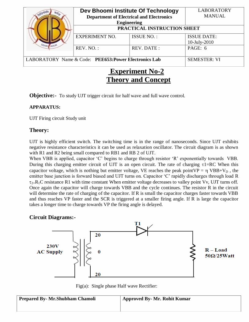
Experiment No-2
Theory and Concept
Objective:- To study UJT trigger circuit for half wave and full wave control.
APPARATUS:
UJT Firing circuit Study unit
Theory:
UJT is highly efficient switch. The switching time is in the range of nanoseconds. Since UJT exhibits
negative resistance characteristics it can be used as relaxation oscillator. The circuit diagram is as shown
with R1 and R2 being small compared to RB1 and RB 2 of UJT.
When VBB is applied, capacitor ‘C’ begins to charge through resistor ‘R’ exponentially towards VBB.
During this charging emitter circuit of UJT is an open circuit. The rate of charging 1=RC When this
capacitor voltage, which is nothing but emitter voltage, VE reaches the peak pointVP = VBB+VD , the
emitter base junction is forward biased and UJT turns on. Capacitor ‘C’ rapidly discharges through load R
2=R1C resistance R1 with time constant When emitter voltage decreases to valley point Vv, UJT turns off.
Once again the capacitor will charge towards VBB and the cycle continues. The resistor R in the circuit
will determine the rate of charging of the capacitor. If R is small the capacitor charges faster towards VBB
and thus reaches VP faster and the SCR is triggered at a smaller firing angle. If R is large the capacitor
takes a longer time to charge towards VP the firing angle is delayed.
Circuit Diagrams:-
Fig(a): Single phase Half wave Rectifier:
Dev Bhoomi Institute Of Technology Department of Electrical and Electronics
Engineering
LABORATORY
MANUAL
PRACTICAL INSTRUCTION SHEET
EXPERIMENT NO. ISSUE NO. : ISSUE DATE:
10-July-2010
REV. NO. : REV. DATE :
PAGE: 7
LABORATORY Name & Code: PEE653:Power Electronics Lab SEMESTER: VI
Prepared By- Mr.Shubham Chamoli Approved By- Mr. Rohit Kumar
Fig(b): Single phase Full wave Rectifier
PROCEDURE:
I. Firing of SCR using UJT for half wave rectifier:-
1) Switch ON the mains supply observe and note down the wave forms at the different points in the circuit
and also the trigger O/ps – T1, & T1’.
2) Make sure that the pulse transformer O/ps T1 & T1’ are proper and synchronized.
3) Now make the connections as given the circuit diagram for Half wave rectifier using AC source,UJT
relaxation Oscillator, SCR(T1)and a suitable load (50Ohms/25wattResistor)
4) Now switch ON the mains supply, observe and note down the output waveforms across load And SCR.
5) Draw the wave forms at different firing angle – 120, 90 & 60 for both Half & full wave rectifier
6) In the UJT firing Circuit the firing angle can be varied from 150degree to 30degree approximately.
7) We cannot vary from exact 0degree to 180degree as we vary in single phase converter firing circuit.
8) This is one of the simplest method of SCR triggering.
9) We can also fire SCR’s in the different Power circuits like Single phase half controlled converter,
Single phase AC voltage controller using both SCR and Triac.
II. Firing of SCR using UJT for Full wave rectifier:- 1) Switch ON the mains supply observe and note down the wave forms at the different points in the circuit
and also the trigger O/ps – T1, & T1’.
2) Make sure that the pulse transformer O/ps T1 & T1’ are proper and synchronized.
Now make the connections as given the circuit diagram for Full wave rectifier
using AC source, UJT relaxation Oscillator, SCR’s(T1andT2)and a suitable
Dev Bhoomi Institute Of Technology Department of Electrical and Electronics
Engineering
LABORATORY
MANUAL
PRACTICAL INSTRUCTION SHEET
EXPERIMENT NO. ISSUE NO. : ISSUE DATE:
10-July-2010
REV. NO. : REV. DATE :
PAGE: 8
LABORATORY Name & Code: PEE653:Power Electronics Lab SEMESTER: VI
Prepared By- Mr.Shubham Chamoli Approved By- Mr. Rohit Kumar
load(50Ohms/25wattResistor)
3) Now switch ON the mains supply, observe and note down the output waveforms across load And SCR.
4) Draw the wave forms at different firing angle – 120, 90 & 60 for both Half & full wave rectifier
5) In the UJT firing Circuit the firing angle can be varied from 150degree to 30degree approximately.
6) We cannot vary from exact 0degree to 180degree as we vary in single phase converter firing circuit.
7) This is one of the simplest method of SCR triggering.
8) We can also fire SCR’s in the different Power circuits like Single phase half controlled converter
,Single phase AC voltage controller using both SCR and Triac.
a. UJT Relaxation Oscillator:
1) To Study oscillator using UJT, short CF to the diode bridge rectifier to get filtered DC output.
2) Now we will get the equidistant pulses at the o/p of pulse transformer.
3) The frequency of the pulses can be varied by varying the potentiometer RC.
4) Draw the wave forms at different points by varying RC.
Observation Table:
Table1:- Synchronized UJT triggering circuit for HWR:-
Table 2: Synchronized UJT triggering circuit for FWR:-
Dev Bhoomi Institute Of Technology Department of Electrical and Electronics
Engineering
LABORATORY
MANUAL
PRACTICAL INSTRUCTION SHEET
EXPERIMENT NO. ISSUE NO. : ISSUE DATE:
10-July-2010
REV. NO. : REV. DATE :
PAGE: 9
LABORATORY Name & Code: PEE653:Power Electronics Lab SEMESTER: VI
Prepared By- Mr.Shubham Chamoli Approved By- Mr. Rohit Kumar
NOTE:- a) At lower firing angles SCR may not turn on due to the fact that UJT takes some time (charging
time) to generate first firing pulse. b)At higher firing angles SCR may not turn on due to the fact that VAK
is insufficient to turn-on SCR.
RESULT:- UJT Relaxation oscillator and UJT HALF & FULL WAVE CONTROLLED CIRCUITS is
constructed and its performance is studied
Dev Bhoomi Institute Of Technology Department of Electrical and Electronics
Engineering
LABORATORY
MANUAL
PRACTICAL INSTRUCTION SHEET
EXPERIMENT NO. ISSUE NO. : ISSUE DATE:
10-July-2010
REV. NO. : REV. DATE :
PAGE: 10
LABORATORY Name & Code: PEE653:Power Electronics Lab SEMESTER: VI
Prepared By- Mr.Shubham Chamoli Approved By- Mr. Rohit Kumar
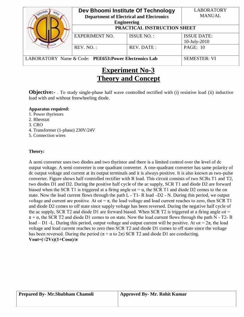
Experiment No-3
Theory and Concept
Objective:- . To study single-phase half wave controlled rectified with (i) resistive load (ii) inductive
load with and without freewheeling diode.
Apparatus required: 1. Power thyristors
2. Rheostat
3. CRO
4. Transformer (1-phase) 230V/24V
5. Connection wires
Theory:
A semi converter uses two diodes and two thyristor and there is a limited control over the level of dc
output voltage. A semi converter is one quadrant converter. A one-quadrant converter has same polarity of
dc output voltage and current at its output terminals and it is always positive. It is also known as two-pulse
converter. Figure shows half controlled rectifier with R load. This circuit consists of two SCRs T1 and T2,
two diodes D1 and D2. During the positive half cycle of the ac supply, SCR T1 and diode D2 are forward
biased when the SCR T1 is triggered at a firing angle ωt = α, the SCR T1 and diode D2 comes to the on
state. Now the load current flows through the path L - T1- R load –D2 - N. During this period, we output
voltage and current are positive. At ωt = π, the load voltage and load current reaches to zero, then SCR T1
and diode D2 comes to off state since supply voltage has been reversed. During the negative half cycle of
the ac supply, SCR T2 and diode D1 are forward biased. When SCR T2 is triggered at a firing angle ωt =
π + α, the SCR T2 and diode D1 comes to on state. Now the load current flows through the path N - T2- R
load – D1 -L. During this period, output voltage and output current will be positive. At ωt = 2π, the load
voltage and load current reaches to zero then SCR T2 and diode D1 comes to off state since the voltage
has been reversed. During the period (π + α to 2π) SCR T2 and diode D1 are conducting.
Vout=(√2Vs)(1+Cosα)/π
Dev Bhoomi Institute Of Technology Department of Electrical and Electronics
Engineering
LABORATORY
MANUAL
PRACTICAL INSTRUCTION SHEET
EXPERIMENT NO. ISSUE NO. : ISSUE DATE:
10-July-2010
REV. NO. : REV. DATE :
PAGE: 11
LABORATORY Name & Code: PEE653:Power Electronics Lab SEMESTER: VI
Prepared By- Mr.Shubham Chamoli Approved By- Mr. Rohit Kumar
Circuit Diagram:
Procedure:
1. Make the connections as per the circuit diagram.
2. Connect CRO and voltmeter across the load.
3. Keep the potentiometer at the minimum position.
4. Switch on the step down ac source.
5. Check the gate pulses at G1-K1 & G2-K2, respectively.
6. Observe the wave form on CRO and note the triggering angle ‘α’ and
7. Note the corresponding reading of the voltmeter. Also note the value of Maximum amplitude Vm from
the waveform.
8. Set the potentiometer at different positions and follow the step given in (6) for every position.
9. Tabulate the readings in the observation column.
Dev Bhoomi Institute Of Technology Department of Electrical and Electronics
Engineering
LABORATORY
MANUAL
PRACTICAL INSTRUCTION SHEET
EXPERIMENT NO. ISSUE NO. : ISSUE DATE:
10-July-2010
REV. NO. : REV. DATE :
PAGE: 12
LABORATORY Name & Code: PEE653:Power Electronics Lab SEMESTER: VI
Prepared By- Mr.Shubham Chamoli Approved By- Mr. Rohit Kumar
Waveform:
Observation Table:
Result: Thus the operation of single phase half controlled converter using R and RL load has studied and the
output waveforms has been observed.
Dev Bhoomi Institute Of Technology Department of Electrical and Electronics
Engineering
LABORATORY
MANUAL
PRACTICAL INSTRUCTION SHEET
EXPERIMENT NO. ISSUE NO. : ISSUE DATE:
10-July-2010
REV. NO. : REV. DATE :
PAGE: 13
LABORATORY Name & Code: PEE653:Power Electronics Lab SEMESTER: VI
Prepared By- Mr.Shubham Chamoli Approved By- Mr. Rohit Kumar
Experiment No-4
Theory and Concept
Objective:- . To study single phase (i) fully controlled (ii) half controlled bridge rectifiers with resistive
and inductive loads
Apparatus required: 1. Power thyristors
2. Rheostat
3. CRO
4. Transformer (1-phase) 230V/24V
5. Connection wires
Theory:-
Phase controlled AC-DC converters employing thyristor are extensively used for changing constant ac
input voltage to controlled dc output voltage. In phase-controlled rectifiers, a thyristor is tuned off as AC
supply voltage reverse biases it, provided anode current has fallen to level below the holding current.
Controlled rectifiers have a wide range of applications, from small rectifiers to large high voltage direct
current (HVDC) transmission systems. They are used for electrochemical processes, many kinds of motor
drives, traction equipment, controlled power supplies, and many other applications.
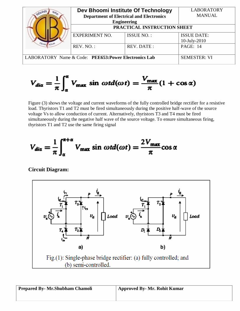
Single-Phase Full-Wave Controlled Rectifier
Once of the types of controlled rectifier is fully controlled and semiconductor rectifier. A fully-controlled
circuit contains only thyristers (semiconductor controlled rectifiers (SCR)), whereas a semi-controlled
rectifier circuit is made up of both SCR and diodes as shown in Fig.(1). Due to presence of diodes, free-
wheeling operation takes place without allowing the bridge output voltage to become negative.
In a semi-controlled rectifier, control is affected only for positive output voltage, and no control is
possible when its output voltage tends to become negative since it is clamped at zero volts.
As shown in Fig. (2), thyristor T1 can be fired into the ON state at any time provided that voltage vT1 > 0.
The firing pulses are delayed by an angle a with respect to the instant where diodes would conduct.
Thyristor T1 remains in the ON state until the load current tries to go to a negative value. Thyristor T2 is
fired into the ON state when vT2 > 0, which corresponds in Fig. (2) to the condition at which v2 > 0. The
mean value of the load voltage with resistive load is given by:
Dev Bhoomi Institute Of Technology Department of Electrical and Electronics
Engineering
LABORATORY
MANUAL
PRACTICAL INSTRUCTION SHEET
EXPERIMENT NO. ISSUE NO. : ISSUE DATE:
10-July-2010
REV. NO. : REV. DATE :
PAGE: 14
LABORATORY Name & Code: PEE653:Power Electronics Lab SEMESTER: VI
Prepared By- Mr.Shubham Chamoli Approved By- Mr. Rohit Kumar
Figure (3) shows the voltage and current waveforms of the fully controlled bridge rectifier for a resistive
load. Thyristors T1 and T2 must be fired simultaneously during the positive half-wave of the source
voltage Vs to allow conduction of current. Alternatively, thyristors T3 and T4 must be fired
simultaneously during the negative half wave of the source voltage. To ensure simultaneous firing,
thyristors T1 and T2 use the same firing signal
Circuit Diagram:
Dev Bhoomi Institute Of Technology Department of Electrical and Electronics
Engineering
LABORATORY
MANUAL
PRACTICAL INSTRUCTION SHEET
EXPERIMENT NO. ISSUE NO. : ISSUE DATE:
10-July-2010
REV. NO. : REV. DATE :
PAGE: 15
LABORATORY Name & Code: PEE653:Power Electronics Lab SEMESTER: VI
Prepared By- Mr.Shubham Chamoli Approved By- Mr. Rohit Kumar
Procedure:
1. Connect the single phase full wave controlled rectifier circuit shown in Fig.(1-a) on the power electronic trainer.
2. Turn on the power
3. Plot the input and output waveforms on the same graph paper.
4. Measure the average and RMS output voltage by connect the AVO meter across load resistance.
5. Turn off the power
Waveforms:
Dev Bhoomi Institute Of Technology Department of Electrical and Electronics
Engineering
LABORATORY
MANUAL
PRACTICAL INSTRUCTION SHEET
EXPERIMENT NO. ISSUE NO. : ISSUE DATE:
10-July-2010
REV. NO. : REV. DATE :
PAGE: 16
LABORATORY Name & Code: PEE653:Power Electronics Lab SEMESTER: VI
Prepared By- Mr.Shubham Chamoli Approved By- Mr. Rohit Kumar
The following tasks you can perform through alter table command.
Dev Bhoomi Institute Of Technology Department of Electrical and Electronics
Engineering
LABORATORY
MANUAL
PRACTICAL INSTRUCTION SHEET
EXPERIMENT NO. ISSUE NO. : ISSUE DATE:
10-July-2010
REV. NO. : REV. DATE :
PAGE: 17
LABORATORY Name & Code: PEE653:Power Electronics Lab SEMESTER: VI
Prepared By- Mr.Shubham Chamoli Approved By- Mr. Rohit Kumar
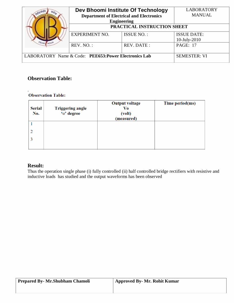
Observation Table:
.
Result: Thus the operation single phase (i) fully controlled (ii) half controlled bridge rectifiers with resistive and
inductive loads has studied and the output waveforms has been observed
Dev Bhoomi Institute Of Technology Department of Electrical and Electronics
Engineering
LABORATORY
MANUAL
PRACTICAL INSTRUCTION SHEET
EXPERIMENT NO. ISSUE NO. : ISSUE DATE:
10-July-2010
REV. NO. : REV. DATE :
PAGE: 18
LABORATORY Name & Code: PEE653:Power Electronics Lab SEMESTER: VI
Prepared By- Mr.Shubham Chamoli Approved By- Mr. Rohit Kumar
Experiment No-5
Theory & Concept
Objective:- To study three-phase fully/half controlled bridge rectifier with resistive and inductive loads
Apparatus Required: 1. Power electronic trainer.
2. Connection wires.
3. Oscilloscope.
Theory: Phase controlled AC-DC converters employing thyristor are extensively used for changing constant ac
input voltage to controlled dc output voltage. In phasecontrolled rectifiers, a thyristor is tuned off as AC
supply voltage reverse biases it, provided anode current has fallen to level below the holding current.
Controlled rectifiers have a wide range of applications, from small rectifiers to large high voltage direct
current (HVDC) transmission systems. They are used for electrochemical processes, many kinds of motor
drives, traction equipment, controlled power supplies, and many other applications Three- phase Full
wave controlled rectifier: Fig(1-a) shows the three-phase bridge rectifier. The configuration does not need
any special transformer, and works as a 6-pulse rectifier. The series characteristic of this rectifier produces
a dc voltage twice the value of the half-wave rectifier .
The load average voltage is given by:
Dev Bhoomi Institute Of Technology Department of Electrical and Electronics
Engineering
LABORATORY
MANUAL
PRACTICAL INSTRUCTION SHEET
EXPERIMENT NO. ISSUE NO. : ISSUE DATE:
10-July-2010
REV. NO. : REV. DATE :
PAGE: 19
LABORATORY Name & Code: PEE653:Power Electronics Lab SEMESTER: VI
Prepared By- Mr.Shubham Chamoli Approved By- Mr. Rohit Kumar
Fig(3) shows the voltages of each half-wave bridge of this topology and , the total instantaneous dc
voltage vD, and the anode-to-cathode voltage vAK in one of the bridge thyristors. The maximum value of
vak= √3 Vmax, which is the same as that of the half-wave converter
Circuit Diagram:
Dev Bhoomi Institute Of Technology Department of Electrical and Electronics
Engineering
LABORATORY
MANUAL
PRACTICAL INSTRUCTION SHEET
EXPERIMENT NO. ISSUE NO. : ISSUE DATE:
10-July-2010
REV. NO. : REV. DATE :
PAGE: 20
LABORATORY Name & Code: PEE653:Power Electronics Lab SEMESTER: VI
Prepared By- Mr.Shubham Chamoli Approved By- Mr. Rohit Kumar
Procedure:
1. Connect the three-phase full wave controlled rectifier circuit shown in Fig.(1-a) on the power electronic
trainer.
2. Turn on the power
3. By use oscilloscope, plot the input and output waveforms on the same graph paper" same axis".
4. Measure the average and RMS output voltage by connect the AVO meter across load resistance.
5. Turn off the power
6. Use an inductive load. With L=100mH measure the output voltage and plot the output waveform.
7. Repeat step 6 with L=100mH measure the output voltage and plot the output waveforms.
8. Repeat step 6 & 7 with connect the freewheeling diode across the load.
9. Connect the three-phase bridge half-control rectifier circuit shown in Fig.(1- b).
10. Repeat steps (2-7).
Observation Table:
Dev Bhoomi Institute Of Technology Department of Electrical and Electronics
Engineering
LABORATORY
MANUAL
PRACTICAL INSTRUCTION SHEET
EXPERIMENT NO. ISSUE NO. : ISSUE DATE:
10-July-2010
REV. NO. : REV. DATE :
PAGE: 21
LABORATORY Name & Code: PEE653:Power Electronics Lab SEMESTER: VI
Prepared By- Mr.Shubham Chamoli Approved By- Mr. Rohit Kumar
Waveforms:
Result: Thus the operation of three-phase fully/half controlled bridge rectifier with resistive and
inductive loads and waveforms are observed.
Dev Bhoomi Institute Of Technology Department of Electrical and Electronics
Engineering
LABORATORY
MANUAL
PRACTICAL INSTRUCTION SHEET
EXPERIMENT NO. ISSUE NO. : ISSUE DATE:
10-July-2010
REV. NO. : REV. DATE :
PAGE: 22
LABORATORY Name & Code: PEE653:Power Electronics Lab SEMESTER: VI
Prepared By- Mr.Shubham Chamoli Approved By- Mr. Rohit Kumar
Experiment No-6
Theory & Concept
Objective:- To study single-phase ac voltage regulator with resistive and inductive loads
Apparatus required: Trainer Kit
CRO
Patch chords
Theory:
R- Load An AC voltage regulator consists of two SCRs connected in anti parallel During positive half cycle, the
SCR2 is forward biased. The current flow is through terminal P – SCR2 – the load and the terminal N.
During the negative half cycle the SCR1 is forward biased. The current flow is through terminal N –
SCR2 – load –terminal P.
The firing angle of the SCRs is kept at 450 If tha delay angles of the two SCRs are equal, and the input
voltage is Vm sinωt, the RMS output voltage will be given by formula stated in model calculation.
Thus by varying α from 0 to π, the RMS value of output voltage can be controlled from RMS input
voltage to 0
R- L Load
During the positive half cycle SCR2 is triggered into a firing angle delay of α, the current rises slowly due
to the inductor. The current continues to flow even after the supply voltage reverses, due to the energy
stored in the inductor.
As long as the SCR2 conducts, the conduction drop across it will reverse bias SCR1 , hence it will not
conduct even if gating signal is applied. It can be triggered into conduction during the negative half cycle
after SCR2 turns OFF. The wave forms are shown for both
continuous and discontinuous current
Dev Bhoomi Institute Of Technology Department of Electrical and Electronics
Engineering
LABORATORY
MANUAL
PRACTICAL INSTRUCTION SHEET
EXPERIMENT NO. ISSUE NO. : ISSUE DATE:
10-July-2010
REV. NO. : REV. DATE :
PAGE: 23
LABORATORY Name & Code: PEE653:Power Electronics Lab SEMESTER: VI
Prepared By- Mr.Shubham Chamoli Approved By- Mr. Rohit Kumar
Circuit Diagram:
Dev Bhoomi Institute Of Technology Department of Electrical and Electronics
Engineering
LABORATORY
MANUAL
PRACTICAL INSTRUCTION SHEET
EXPERIMENT NO. ISSUE NO. : ISSUE DATE:
10-July-2010
REV. NO. : REV. DATE :
PAGE: 24
LABORATORY Name & Code: PEE653:Power Electronics Lab SEMESTER: VI
Prepared By- Mr.Shubham Chamoli Approved By- Mr. Rohit Kumar
Procedure: R –Load
1. Connect anode of SCR2 to the cathode of SCR1
2. Connect the 24V AC positive terminal to anode of SCR2
3. Connect R load terminal between cathode of SCR1 and 24V AC output.
4. Connect the CRO across the load
5. Connect the voltmeter across the load terminals
6. Connect G2 & K2 of firing circuit to G2 & K2 of SCR 2
7. Switch ON the trainer kit
8. Place the switch S2 in SCR mode
9. Switch ON the 24V AC supply
10. Switch ON the denounce switch.
11. Note down the peak value of voltage Vm , triggering angle α and conduction angle γ
12. By varying the firing angle the output can be varied
13. Plot the graph Vm versus α and γ
RL – Load
1. Connect R and L in series then connect the load terminals between cathode of SCR1 and 24V ac input.
2. Repeat the above steps
3. Observe the waveforms
Observation Table:
Dev Bhoomi Institute Of Technology Department of Electrical and Electronics
Engineering
LABORATORY
MANUAL
PRACTICAL INSTRUCTION SHEET
EXPERIMENT NO. ISSUE NO. : ISSUE DATE:
10-July-2010
REV. NO. : REV. DATE :
PAGE: 25
LABORATORY Name & Code: PEE653:Power Electronics Lab SEMESTER: VI
Prepared By- Mr.Shubham Chamoli Approved By- Mr. Rohit Kumar
Waveform:
Dev Bhoomi Institute Of Technology Department of Electrical and Electronics
Engineering
LABORATORY
MANUAL
PRACTICAL INSTRUCTION SHEET
EXPERIMENT NO. ISSUE NO. : ISSUE DATE:
10-July-2010
REV. NO. : REV. DATE :
PAGE: 26
LABORATORY Name & Code: PEE653:Power Electronics Lab SEMESTER: VI
Prepared By- Mr.Shubham Chamoli Approved By- Mr. Rohit Kumar
Results: The SCR based single phase AC voltage controller or regulator with R & RL load is studied and the
required graphs are plotted.
Dev Bhoomi Institute Of Technology Department of Electrical and Electronics
Engineering
LABORATORY
MANUAL
PRACTICAL INSTRUCTION SHEET
EXPERIMENT NO. ISSUE NO. : ISSUE DATE:
10-July-2010
REV. NO. : REV. DATE :
PAGE: 27
LABORATORY Name & Code: PEE653:Power Electronics Lab SEMESTER: VI
Prepared By- Mr.Shubham Chamoli Approved By- Mr. Rohit Kumar
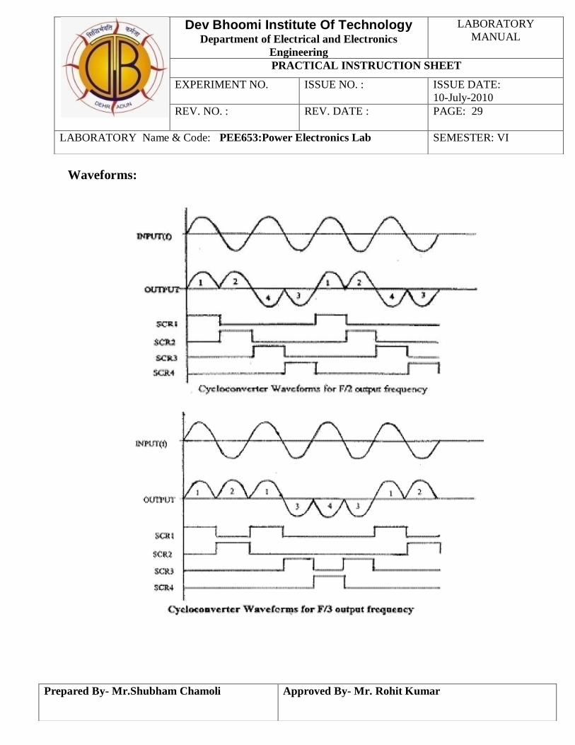
Experiment No-7
Theory & Concept
Objective:- To study single phase cyclo-converter.


![Computer Graphics. Lab Manual - dbit.ac.in · [Type the document title] Dev Bhoomi Institute Of Technology Tushar Anthwal Page 2 Computer Graphics Lab. 1. Syllabus from the university](https://static.documents.pub/doc/80x56/5d4fba3588c993374f8b6a30/computer-graphics-lab-manual-dbitacin-type-the-document-title-dev-bhoomi.jpg)


