Experimental Techniques for the Mechanical Characterization of One-Dimensional Nanostructures Y. Zhu & C. Ke & H.D. Espinosa Received: 7 March 2006 / Accepted: 15 September 2006 / Published online: 11 January 2007 # Society for Experimental Mechanics 2007 Abstract New materials and nanostructures with su- perior electro-mechanical properties are emerging in the development of novel devices. Engineering appli- cation of these materials and nanostructures requires accurate mechanical characterization, which in turn requires development of novel experimental tech- niques. In this paper, we review some of the existing experimental techniques suitable to investigate the mechanics of one-dimensional (1D) nanostructures. Particular emphasis is placed on techniques that allow comparison of quantities measured in the tests with predictions arising from multiscale computer simula- tions on a one to one basis. We begin with an overview of major challenges in the mechanical characterization of 1D nanostructures, followed by a discussion of two distinct types of experimental techniques: nanoinden- tation/atomic force microscopy (AFM) and in-situ electron microscopy testing. We highlight a recently developed in-situ transmission and scanning electron microscopy testing technique, for investigating the mechanics of thin films and 1D nanostructures, based on microelectromechanical systems (MEMS) technol- ogy. We finally present the coupled field (electro and mechanical) characterization of a NEMS bistable switch in-situ a scanning electron microscope (SEM). Keywords Nanomechanics . In-situ microscopy . MEMS . Carbon nanotubes . Nanowires . NEMS Introduction The discovery of carbon nanotubes (CNTs) by Iijima in the early 1990s sparked an entirely new paradigm for making devices and elicited major fundamental developments within science and technology [1]. Nanowires, nanotubes, and nanobelts of a variety of materials were successfully synthesized and then employed in manufacturing prototype devices in the lab [2, 3]. These nanostructures exhibited not only outstanding mechanical properties [4] but also unique electrical [5], thermal [6] and optical properties [7]. As such, they were envisioned in applications where either material multifunctionality is desirable (e.g., nano- composites [8]) or in those where new architectures are required to achieve major performance enhance- ments (e.g., nano-motors [9], nano-switches [10] and nano-sensors [11]). From an engineering viewpoint, electro-mechanical characterization of these nano- structures is essential for the reliable design of such devices. It is well known that strong size dependent mechan- ical properties arise as the characteristic dimension of the structure approaches or is smaller than 100 nm. This has greatly motivated the mechanics community to investigate nanoscale mechanical behavior from both computational and experimental perspectives. An interesting feature emerging from the mechanics of nanostructures is that they provide an excellent platform for gaining insight into fundamental mecha- nisms of material deformation and failure. Indeed, the systems contain a limited number of atoms and possible equilibrium configurations, which can be identified in real time by means of in-situ X-ray and transmission electron microscopy (TEM). In addition, Experimental Mechanics (2007) 47: 7–24 DOI 10.1007/s11340-006-0406-6 Y. Zhu : C. Ke : H.D. Espinosa (*, SEM member) Department of Mechanical Engineering, Northwestern University, 2145 Sheridan Road, Evaston, IL 60208-3111, USA e-mail: [email protected]SEM
Transcript
Experimental Techniques for the MechanicalCharacterization of One-Dimensional Nanostructures
Y. Zhu & C. Ke & H.D. Espinosa
Received: 7 March 2006 /Accepted: 15 September 2006 / Published online: 11 January 2007# Society for Experimental Mechanics 2007
Abstract New materials and nanostructures with su-
perior electro-mechanical properties are emerging in
the development of novel devices. Engineering appli-
cation of these materials and nanostructures requires
accurate mechanical characterization, which in turn
requires development of novel experimental tech-
niques. In this paper, we review some of the existing
experimental techniques suitable to investigate the
mechanics of one-dimensional (1D) nanostructures.
Particular emphasis is placed on techniques that allow
comparison of quantities measured in the tests with
predictions arising from multiscale computer simula-
tions on a one to one basis. We begin with an overview
of major challenges in the mechanical characterization
of 1D nanostructures, followed by a discussion of two
distinct types of experimental techniques: nanoinden-
tation/atomic force microscopy (AFM) and in-situ
electron microscopy testing. We highlight a recently
developed in-situ transmission and scanning electron
microscopy testing technique, for investigating the
mechanics of thin films and 1D nanostructures, based
on microelectromechanical systems (MEMS) technol-
ogy. We finally present the coupled field (electro and
mechanical) characterization of a NEMS bistable
switch in-situ a scanning electron microscope (SEM).
Keywords Nanomechanics . In-situ microscopy .
MEMS . Carbon nanotubes . Nanowires . NEMS
Introduction
The discovery of carbon nanotubes (CNTs) by Iijima
in the early 1990s sparked an entirely new paradigm
for making devices and elicited major fundamental
developments within science and technology [1].
Nanowires, nanotubes, and nanobelts of a variety of
materials were successfully synthesized and then
employed in manufacturing prototype devices in the
lab [2, 3]. These nanostructures exhibited not only
outstanding mechanical properties [4] but also unique
electrical [5], thermal [6] and optical properties [7]. As
such, they were envisioned in applications where either
material multifunctionality is desirable (e.g., nano-
composites [8]) or in those where new architectures
are required to achieve major performance enhance-
ments (e.g., nano-motors [9], nano-switches [10] and
nano-sensors [11]). From an engineering viewpoint,
electro-mechanical characterization of these nano-
structures is essential for the reliable design of such
devices.
It is well known that strong size dependent mechan-
ical properties arise as the characteristic dimension of
the structure approaches or is smaller than 100 nm.
This has greatly motivated the mechanics community
to investigate nanoscale mechanical behavior from
both computational and experimental perspectives.
An interesting feature emerging from the mechanics
of nanostructures is that they provide an excellent
platform for gaining insight into fundamental mecha-
nisms of material deformation and failure. Indeed, the
systems contain a limited number of atoms and
possible equilibrium configurations, which can be
identified in real time by means of in-situ X-ray and
transmission electron microscopy (TEM). In addition,
Experimental Mechanics (2007) 47: 7–24
DOI 10.1007/s11340-006-0406-6
Y. Zhu :C. Ke :H.D. Espinosa (*, SEM member)Department of Mechanical Engineering, NorthwesternUniversity, 2145 Sheridan Road,Evaston, IL 60208-3111, USAe-mail: [email protected]
SEM
because of the limited number of atoms, these systems
can be atomistically modeled within the reach of
currently available computational power. For instance,
CNTs offer a unique system for the study of fracture at
the atomic scale because fracture of a single molecule
involves only chemical bonds breaking at this scale
without other structural complications such as grain
boundaries [12]. Likewise, single crystalline metallic
nanowires provide the opportunity to investigate
dislocation nucleation and their mutual interaction or
interaction with surfaces [13]. Therefore, from a
scientific viewpoint, direct comparison between nano-
mechanical tests and atomistic simulations on a one-to-
one basis becomes feasible and has the potential to
lead to important new discoveries in the context of
system reliability.
While theory and simulations are based on somewhat
developed theories such as quantum mechanics and
molecular mechanics, the experimental techniques used
to investigate the mechanics of nanostructures is much
less evolved in spite of the fact that some important
progress has been made [4, 14, 15]. Moreover, current
experimental data are either insufficient or inconsis-
tent, which suggest the need for efforts in developing
standardized nanomechanical testing methods.
In this paper, we review recent advances in exper-
imental techniques for nano-mechanical testing, main-
ly focusing on one-dimensional (1D) nanostructures.
We begin by providing an overview of major chal-
lenges in the mechanical characterization of 1D nano-
structures. Next, we group the available experimental
techniques into two categories: nanoindentation/atom-
ic force microscopy (AFM) and in-situ electron
microscopy testing. We discuss these techniques with
special emphasis on specimen fabrication, load/dis-
placement resolutions, and real time imaging capabil-
ities. In particular, we highlight two novel in-situ
electron microscopy testing techniques recently devel-
oped in our lab: a nanoscale material testing system (n-
MTS) and in-situ SEM electromechanical testing of
NEMS. Finally, we close the article with concluding
remarks and future research directions.
Challenges in the Mechanical Characterizationof 1D Nanostructures
Property measurements of 1D nanostructures, such
as nanowires and CNTs, are extremely challenging be-
cause of their miniscule size. As such, early studies
of their mechanical properties focused on theoreti-
cal analyses and numerical simulations. Owing to ad-
vances in scanning probe and electron microscopies,
nanoscale experimental techniques utilizing these
tools have been developed. The main challenges in
the experimental study of 1D nanostructures include:
(1) manufacturing, manipulation and positioning of
specimens with nanometer accuracy; (2) application
and measurement of forces in the nano-Newton level,
and (3) measurement of mechanical deformation with
nanometer resolution.
Manipulation and Positioning of Specimens
One of the key steps in nanoscale mechanical testing is
the manipulation and positioning, with nanometer
resolution and high throughput, of specimens at
desired locations. For tensile testing, this becomes
even more challenging compared to other types of
testing methods, since the specimens must be free-
standing and clamped at both ends. Methods for
manipulation and positioning of nanostructures are
briefly summarized next.
Random dispersion
In this technique, a small aliquot of the 1D nano-
structures in suspension is dropped onto a surface
containing prefabricated trenches or holes. Statistically,
some of the nanostructures are suspended across the
gap with random orientation. Typically such configura-
tion is identified by SEM and the end of the nano-
structure fixed to the substrate by electron beam induced
deposition (EBID) of a gas precursor. Examples are
carbon residues present in a scanning electron microscope
(SEM) chamber [4], and external precursors such as
employed, in combination with atomic probe microsco-
py, for the bending testing of nanostructures.
Nanomanipulation
Commonly two tools are employed for nanomanipula-
tion: AFMs and multiaxes manipulators. AFM was
used to both image and manipulate carbon nanotubes
and nanowires. A BNanoManipulator^ AFM system,
comprising an advanced visual interface for manual
control of the AFM tip and tactile presentation of the
AFM data, was developed [17]. In addition, Veeco
Instruments (Woodbury, New York) developed the
BNanoMan^ system for high-resolution imaging, high
definition nanolithography and direct nanoscale in-
plane manipulation.
Electron microscopy provides the imaging capabil-
ity for manipulating nanostructures with nanometer
8 Exp Mech (2007) 47: 7–24
SEM
resolution. Various nanomanipulators, based on multi-
axes piezo actuation, were designed to work inside either
SEMs [4, 18] or TEMs [19, 20], see Fig. 1(a). These
manipulators are usually composed of both a coarse
micrometer-resolution translation stage and a fine nano-
meter-resolution translation stage, with the latter based
on piezo-driven mechanisms capable of subnanometer
motions. The manipulators typically have the capability
of motion in three linear degrees of freedom, and some
possess additional rotational degrees of freedom.
External field alignment
DC and AC/DC electric fields were used for the
alignment of nanowires [21], nanotubes [22, 23] and
bioparticles [24]. Microfabricated electrodes are typi-
cally used to create electric field gradients in the gap
between them. A droplet containing nanostructures in
suspension is dispensed into the gap with a micropi-
pette. The applied electric field aligns the nanostruc-
tures, due to the dielectrophoresis effect, which results
in the bridging of the electrodes by a single nano-
structure, see Fig. 1(b). Certain electric circuits were
used to ensure the manipulation of one single nano-
structure [23, 24].
Huang et al. [25] demonstrated another method for
aligning nanowires. A laminar flow was employed to
achieve preferential orientation of nanowires on
chemically patterned surfaces. Magnetic fields have
also been used to align carbon nanotubes [26].
Directed self-assembly
Self-assembly is a method of constructing nanostruc-
tures by forming stable bonds between organic or non-
organic molecules and substrates. Rao et al. [27]
reported an approach for large-scale assembly of
carbon nanotubes with high-throughput. Dip Pen
Nanolithography (DPN) [28], was employed to func-
tionalize the specific surface regions either with polar
chemical groups such as amino (–NH2/–NH3+) or
carboxyl (–COOH/–COOj), or with non-polar groups
such as methyl (–CH3). When the substrate with
functionalized surfaces was dipped into a liquid
suspension containing carbon nanotubes, the nano-
tubes were attracted towards the polar regions and
self-assembled to form pre-designed structures, usually
within 10 s, with a yield higher than 90%, see Fig. 1(c).
The reported method is scalable to large arrays of
nanotube devices by using high-throughput patterning
Fig. 1 (a) A MWNT acrossthe gap in a freestandingMEMS device by a nanoma-nipulator (scale bar: 5 mm).(b) A MWNT across the gapbetween two electrodes byelectric field alignment (scalebar: 2.73 mm) (Reprinted withpermission from [23]. * 2003Elsevier Ltd.). (c) Topogra-phy (30�30 mm2) of an arrayof individual SWNTs by di-rect-assembly method. Thefriction-force image (inset)shows a single SWNT (darkline), and the regions con-taining 2-mercaptoimidazole(bright area) and ODT (darkarea) (Reprinted with per-mission from [27]. * 2003Nature Publishing Group).(d) A 2-nm diameter individ-ual SWNT bridging twoislands by direct growthmethod. The bright regions atthe upper right and lower-leftcorners of the image are theedges of two diagonal islands(scale bar: 500 nm) (Reprin-ted with permission from [31].* 1998 Nature PublishingGroup)
Exp Mech (2007) 47: 7–24 9
SEM
methods such as photolithography, stamping or mas-
sively parallel DPN or nano fountain probes (NFP) [29].
Direct growth
Instead of manipulating and aligning nanostructures
after their synthesis, researchers also examined meth-
ods for controlled direct growth. Dai and co-workers
[30, 31] reported several growth approaches for CNTs.
The idea is to pattern a catalyst in an arrayed fashion
and control the growth of CNTs between specific
catalytic sites, see Fig. 1(d). He et al. [32] recently
succeeded in direct growth of Si nanowires between
two preexisting single-crystal Si microelectrodes with
<111> sidewalls. The catalysts were deposited on the
sidewalls of the electrodes and Si epitaxially grown
perpendicularly to the <111> surfaces.
Direct growth is a very promising method to
prepare specimens for nanomechanical characteriza-
tion. It does not involve the nano-welding steps used in
EBID technique, which brings foreign materials, e.g.,
carbon and platinum, onto the surface of nanostruc-
tures. Such contamination might cause some spurious
effects on the properties being measured.
High Resolution Displacement and Force
Measurements
Various microscopy techniques such as SEM, TEM
and AFM, have been widely used in characterizing
nanostructures. These instruments provide effective
ways of measuring dimensions and deformation with
nanometer resolution. Atomic force microscopy uses
a sharp tip at the end of a cantilever, which is driven
by a piezoelectric scanner. The instrument resolution
is a function of the cantilever stiffness, laser beam op-
tical detection, and software for data reduction. Elec-
tron microscopy uses high-energy electron beams for
sample imaging through surface scattering (SEM) and
volume diffraction (TEM). A field emission gun SEM
has a point-to-point resolution of about 1 nm and the
TEM is capable of achieving a point-to-point resolu-
tion of 0.1õ0.2 nm. The resolution of the SEM is
limited by the interaction volume between the electron
beam and the sample surface; while the resolution of
TEM is limited by the spread in energy of the electron
beam, and the quality of the microscope optics. The
imaging capabilities of these instruments have been
used to measure specimen deformation as well as beam
deflection and in turn forces.
Commercial force sensors usually cannot reach
nano-Newton resolution. Therefore, cantilevers have
been effectively employed as force sensors [4, 33],
provided that their spring constants have been accu-
rately calibrated. Alternatively, microfabricated
frames [14] and microelectromechanical systems
(MEMS) [15] offer the capability to measure force
with nano-Newton resolution. We will further discuss
testing devices and their resolution in the section of
BA New MEMS-Based Nanoscale Material Testing
System^.
Experimental Approaches
Mechanical testing at the nanoscale is rapidly evolving
but it remains challenging due to the fact that at least
one characteristic dimension of the specimen is only
within a few hundred nanometers to a few nanometers.
As discussed in the preceding section, specimen
fabrication and/or mounting into the testing devices is
far from trivial. Likewise, load and displacement
measurements with resolutions of nano-Newton (nN)
and nano-meter (nm) or better are required.
From a mechanical characterization viewpoint,
previously developed experimental techniques can be
grouped into two categories: nanoindentation/AFM
testing, and in-situ electron microscopy testing. Nano-
indentation and AFM testing make use of commer-
cially available instruments to apply load and measure
deformation simultaneously. Typically, these instru-
ments load the structure in bending mode, although
other loading conditions can be achieved, as we will
discuss subsequently. In-situ SEM and TEM testing
require special loading stages that can be placed inside
the instruments with the TEM requiring stages only a
few millimeters in size. Due to the point-to-point
resolution of these field emission instruments, these
techniques are probably the most powerful in eluci-
dating deformation mechanisms by real-time imaging
of defect nucleation and propagation. Although a
variety of techniques have been developed for in-situ
TEM testing, few achieve quantitative and simulta-
neous load and deformation measurements. In the
following subsections, we will review these techniques
with a special emphasis on two aspects: 1) fabrication
of specimens including effective approaches to manip-
ulate and position specimens onto miniature loading
stages; 2) testing mode and associated load and
displacement resolutions.
Nanoindentation and Atomic Force Microscopy
A nanoindenter is an instrument that continuously
monitors contact load and position. Using feedback
control and independent sensing of load and displace-
10 Exp Mech (2007) 47: 7–24
SEM
ment, both load and displacement controlled experi-
ments can be performed. Typically, the instrument
load resolution is about 75 nN and the position of the
indenter tip can be determined with an accuracy of
about 0.1 nm. An AFM is an instrument originally
designed to obtain very high-resolution three-dimen-
sional topographical images of surfaces. In an AFM, a
sharp tip at the end of a cantilever is brought into
contact with the sample surface by moving the tip or
sample with piezoelectric-driven scanners. The sam-
ple-tip interaction force causes a cantilever deflection,
which is typically measured by a laser beam impinging
a four quadrant optical detector. Hence, AFM can be
readily applied to mechanical testing by applying force
to the specimen and measuring deformation. The
applied force is computed as the cantilever deflection
times the cantilever stiffness. Since deflection can be
measured with an accuracy within 0.02 nm, for a
typical lever force constant of 10 N/m the force
resolution can be as good as 0.2 nN. It is the load
and displacement resolution of these two instruments
that has been exploited in the nanomechanical char-
acterization of 1D nanostructures. Several experimen-
tal configurations were developed requiring the
preparation of freestanding samples with the proper
boundary conditions and geometric features.
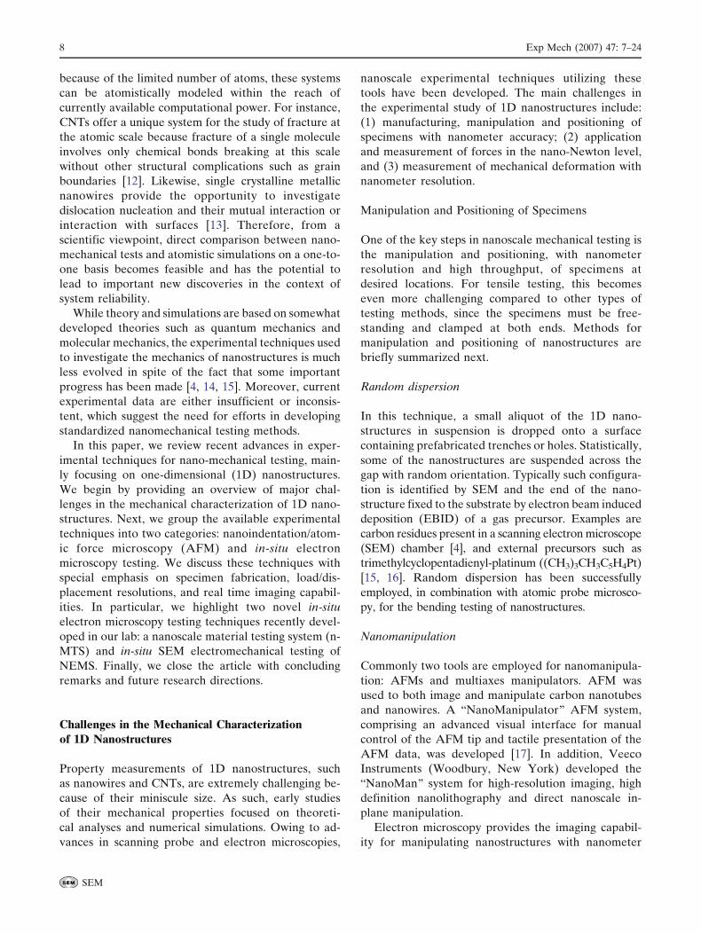
AFM can be operated in several different modes for
the mechanical characterization of 1D nanostructures;
namely, lateral force mode, contact mode, and force
microscopy mode. In the lateral force mode, two
methods of sample preparations and loading config-
urations have been used. In the first method, nano-
structures were dispersed randomly on a substrate and
some of them were pinned selectively by microfabri-
cated islands [34]. Then AFM was used to bend the
cantilevered nanostructures laterally [Fig. 2(a)]. From
the measured load-deflection signatures, the elastic
modulus, strength and toughness were obtained using
continuum mechanics. This technique was applied to
multi-walled carbon nanotubes (MWNTs) and silicon
carbide nanorods [34]. It is straightforward to imple-
ment, however, it cannot eliminate the effect of
adhesion and friction from the substrate. To overcome
this drawback, in the second method, nanostructures
were suspended over a microfabricated trench [35, 36].
The specimens were positioned similarly to the first
method except that one additional step consisting of
the etching of the substrate under the pinned nano-
structure. Another approach consisted in the etching
of a trench followed by random dispersion of nano-
structures around the trench. After a desirable nano-
structure across the trench was identified, EBID of
platinum or other materials was employed to clamp it.
AFM was used to bend the double-clamped nano-
structure laterally, see Fig. 2(b). This technique was
used to test single-walled carbon nanotube ropes [35]
and gold nanowires [36].
In the contact mode, nanostructures are also
clamped at both ends. MWNTs randomly dispersed
on an alumina ultrafiltration membrane with 200 nm
pores were tested in this fashion. The AFM was used
to deflect the suspended nanotubes vertically to obtain
load-deflection signatures, see Fig. 2(c). In this exam-
ple, the adhesion between the nanotubes and the
membrane was found sufficiently strong to fix the
two ends [33].
The force microscopy technique employs essentially
a tensile testing configuration. One end of the speci-
men is attached to the AFM tip and the other end to a
substrate. This technique was applied to measure the
quantized plastic deformation of gold nanowires [37].
As shown in Fig. 2(d), both the AFM cantilever and
the substrate were coated with a thin layer of gold. A
gold nanowire was formed when the AFM cantilever
was pressed against the substrate. A piezo-positioner
was used to displace the substrate and deform the
nanowire in tension. The force was measured from the
cantilever deflection and the deformation of the nano-
wire was determined as the difference between piezo
motion and cantilever deflection. This technique has
also been effectively employed in understanding the
mechanics of single biomolecules, proteins and nano-
fibers [38–40].
Nanoindentation has been used widely in mechan-
ical characterization of thin films. Recently, it has been
extended to testing of 1D nanostructures [41, 42]. The
hardness and elastic modulus of silver nanowires were
measured using a Hysitron Troboscope nanoindenter
[41]. The nanowires were simply dispersed on the
substrate. An array of nanoscale indents were success-
fully made on the wire by direct indention. It was
found that the silver nanowire has comparable hard-
ness and elastic modulus to bulk silver [41]. However,
since the geometry of indentation of a nanowire differs
significantly from that of a half-space, the standard
Oliver–Pharr method of analysis is not applicable.
Instead, a contact model was developed for the
interpretation of nanowire nanoindentation on a flat
substrate. Following this new model, Nix and co-
workers measured the hardness of GaN and ZnO
nanowires [42]. In addition, Waters et al. investigated
the shell buckling of individual MWNT using this
technique [43]. For the nanoindentation test, the
sample preparation is relatively simple; however, the
testing requires very careful and precise alignment and
positioning of the indenter tip. Moreover, due to the
Exp Mech (2007) 47: 7–24 11
SEM
comparable size of the indenter tip and the nanowire
diameter, the contact model can still be applied for
data analysis.
Besides nanoindentation, it is worth mentioning two
innovative applications of nanoindenters in mechanical
characterization: thin film tension and micro-pillar
compression. In the first method, so called membrane
deflection experiment (MDE), the nanoindenter load
and displacement measurement capabilities were
employed to perform tensile testing of freestanding
thin films by means of a loading configuration and
specimen design in which membrane stressing is
achieved. The test consists of transversely loading a
membrane fixed at both ends and spanning a micro-
machined window, Fig. 3(a,b). The membrane has a
double dog bone shape such that bending effects at the
ends and where the load is applied do not control
failure [44]. In this configuration a line-load at the
center of the span is applied to impose a prescribed
deflection history. Simultaneously, an interferometer
focused on the bottom side of the membrane records
deflection and local deformation. The result is direct
tension in the gauged regions of the membrane with
load and deflection being measured independently
[45]. By means of this technique strong size effects in
plasticity and fracture of freestanding polycrystalline
face-center cubic (FCC) thin films were identified [46].
The testing methodology was recently extended to
study fracture toughness of freestanding thin films [47].
The nanoindenter was also employed in the com-
pression testing of micro-pillars. The pillars were
fabricated from a bulk single crystal using FIB [48] or
were electroplated [49]. Using the displacement con-
trol capability of the nanoindenter, pillars of various
sizes were loaded in compression and deformed
plastically well into the finite deformation regime, see
tions revealed that when the diameter of the micro-
pillars becomes smaller than a few tens of micrometers,
the basic processes of plastic deformation are signifi-
cantly modified.
Both nanoindenter and AFM techniques were
found to possess the capability to record load–
displacement histories with high resolution and reli-
ability. In addition, sample preparation is fairly
straightforward. However, a major drawback of these
techniques is that in general they do not achieve
sample imaging while the test is being performed, i.e.,
observing the sample deformation process while re-
cording load and displacement is not possible. An
approach to overcome this limitation is the incorpora-
Fig. 2 (a) A cantilever nano-tube deflected by an AFM inthe lateral force mode(Reprinted with permissionfrom [34]. * 1997 AmericanAssociation for the Advance-ment of Science). (b) A dou-ble-clamped nanowiredeflected by an AFM in thelateral force mode (Reprintedwith permission from [36].* 2005 Nature PublishingGroup). (c-1) A MWNT sus-pended over a porous alumi-na membrane; (c-2) TheMWNT deflected verticallyby an AFM in contact mode(Reprinted with permissionfrom [33]. *1999 AmericanPhysical Society). (d) A goldnanowire stretched by anAFM in force microscopymode (Reprinted with per-mission from [37]. * 2000National Academy of Scien-ces USA)
12 Exp Mech (2007) 47: 7–24
SEM
tion of nanoindenter, AFM or other systems, e.g.,
MEMS, inside the SEM and TEM.
In-situ Scanning and Transmission Electron
Microscopy Testing
In-situ SEM and/or TEM testing allows the usage of
high magnifications and in some instances the real
time observation of failure initiation. While in-situ
SEM testing represents a major advance in mechanical
characterization at the nanoscale, atomic resolution
and real time imaging of defect nucleation and
propagation is generally not possible. In-situ TEM
testing is required for this purpose. Over the years, a
large number of in-situ TEM studies were pursued on
thin film samples [51, 52]; however, the limitation of
traditional in-situ TEM is its lack of quantitative load
and displacement measurement capabilities. As we will
discuss below, such capabilities for in-situ TEM testing
have been recently developed. Resonating the speci-
men inside the SEM or TEM by means of electrostatic
fields is a straightforward technique for mechanical
measurements, which has proved to be a useful
method for 1D nanostructures [19]. However, it does
not provide in-situ observation of the specimen defor-
mation history and details about defect initiation and
propagation. Therefore, we will not discuss this
technique in more detail in this paper.
An example of in-situ SEM tensile testing of 1-D
nanostructures, mounted by nanomanipulation on a
loading system, is the testing of MWNTs, which was
performed using double AFM cantilevers in a 5-axes
nanomanipulation system based on piezo-actuation [4],
see Fig. 4(a). An individual nanotube was clamped to
two AFM tips by EBID of carbonaceous material
present inside the SEM chamber. A relatively stiff
cantilever, connected to one of the piezoactuators, was
used to deform the sample while the force was
calculated based on the deflection of a soft cantilever.
The sample deformation was recorded by SEM
imaging. Experiments revealed a Bsword-in-sheath^failure mechanism with fracture of the outer shell
although direct observation of the shell atomic struc-
ture was not possible. Such imaging becomes feasible
when the experiment is performed inside a TEM, as
we will discuss later.
Co-fabricated thin films attached to a loading frame,
containing a beam for load sensing purposes, were
Fig. 3 (a) Experimental set-up for MDE testing. (b) Atypical thin film Au specimenafter tested by MDE. Defor-mation bands and fracture areobserved (Reprinted withpermission from [63]. * 2005National Academy of Scien-ces USA). (c) Experimentalsetup for micro-compressiontesting of FIB-machined mi-cro-pillar. (d) A typical Nispecimen after testing exhib-iting multiple slip lines(Reprinted with permissionfrom [49]. * 2005 ElsevierLtd.)
Exp Mech (2007) 47: 7–24 13
SEM
achieved through microfabrication [14], see Fig. 4(b).
The loading frame design was such that it could be
placed on both SEM and TEM stages. In this
configuration, load is applied by external piezo-actua-
ing at high magnification, which is needed to identify
atomic defect nucleation and propagation. Using this
technique, elastic, plastic, and fracture behavior of
FCC metals with an average grain size of 50 nm was
investigated. Following similar principles, in-situ TEM
nanoindentation of thin films was achieved [53]. The
indenter was mounted on a piezo-actuator but the
system did not possess load measurement capabilities.
Dislocation nucleation and their interaction with
surfaces and other material defects were investigated
using this technique [53].
As stated above, one of the most widely employed
loading mechanisms inside SEM and TEM instruments
is piezo-actuation. This is the case because it can
impose deformation with sub-nanometer motion reso-
lution. However, load sensing must be performed
independently, which is usually achieved by SEM or
TEM imaging of a flexible member attached to the
sample in series. A major limitation of this approach is
that both sample deformation and load are deduced
from the microscopic imaging of the sample and
testing apparatus. When high magnifications are
employed, these two measurements cannot be made
simultaneously. This limitation may be overcome by
sensing load without the need of imaging, for instance,
electronically [54]. Such a device integrating an
actuator and an electronic load sensor has been
recently developed by Espinosa and co-workers.
Details about its design, resolution and measurements
performed with such device are given next.
A New MEMS-Based Nanoscale Material
Testing System
We developed a MEMS-based nanoscale material
testing system (n-MTS) for in situ AFM/SEM/TEM
testing of 1D nanostructures. A unique feature of the
implemented n-MTS is that it incorporates a capacitive
sensor to measure load electronically. This scheme
makes possible the continuous observation of the
specimen deformation and failure, at high magnifica-
tions, while independently measuring the applied load.
The n-MTS can be used to test 1D nanostructures as
well as nanoscale thin films [15, 55].
The n-MTS consists of three parts: actuator, load
sensor, and a co-fabricated specimen or gap for place-
ment of a 1D nanostructures, see Fig. 5(a). Two types of
actuators were employed in the device design: a comb
drive electrostatic actuator and an in-plane thermal
actuator. The comb drive actuator achieves force-control
while the thermal actuator achieves displacement-con-
trol, i.e., it prescribes the specimen displacement as a
function of actuator supplied voltage [56].
Details of the principles used in electrostatic and
thermal actuation, were described by Kahn et al. [57],
Chu et al. [58], and Zhu et al. [56]. The load sensor in
the n-MTS consists of a rigid shuttle with one set of
Fig. 4 (a) A MWNT mounted between two opposing AFM tips and stretched uniaxially (Reprinted with permission from [4]. * 2000American Association for the Advancement of Science). (b) A microfabricated tensile testing frame including a co-fabricatedfreestanding thin film and a force sensor (a slender beam). The chip is actuated by an external piezoelectric actuator (Reprinted withpermission from [14]. * 2004 National Academy of Sciences USA)
14 Exp Mech (2007) 47: 7–24
SEM
movable fingers and two sets of stationary fingers. A
lumped model of the sensor consists of two capacitors
in series. The displacement of the shuttle causes the in-
crease of one capacitance and the decrease of the other.
Within a moderate displacement range, the capacitance
change is proportional to the displacement [54]. The
load sensor is anchored to the substrate by four folded
beams that are designed with a range of stiffness suited
for testing various materials of interest (see Espinosa
et al. [55] for details).
Measuring capacitance changes with sub-femto-
Farad resolution, as required in this application, is
quite challenging. We used the so-called charge
sensing method to overcome this challenge [59]. A
commercially available integrated circuit (IC) based
on this method, Universal Capacitive Readout MS3110
(Microsensors, Costa Mesa, CA), was successfully
employed. In the SEM implementation of the n-MTS,
the MEMS chip was positioned very close to the
sensing IC chip (MS3110) in order to minimize stray
capacitance and electromagnetic interference. Both
chips were placed on a custom-made printed circuit
board with grounded shields on both sides [15, 55], see
Fig. 5(b). In the TEM implementation, Fig. 5(c), the
ization of the MEMS actuator and calibration of the
load sensor was performed in-situ the SEM [15, 54].
We demonstrated the system possesses a displacement
resolution of 1 nm, which translates to a load
resolution of õ12 nN for a sensor stiffness of 11.8 N/m.
Using this two-chip architecture, nanoscale free-
standing polysilicon beams were tested successfully
inside the SEM. A dog-bone shaped Poly-Si specimen
with a trapezoidal cross-section was obtained by nano-
machining using focused ion beam (FIB) (Fig. 6). Two
platinum (Pt) lines (with a spacing of 2.5 mm) were de-
posited by EBID in a dual beam FIB/SEM instrument
(FEI, Hillsboro, Oregon) for deformation measure-
ments. Measured stress–strain curves are shown in
Fig. 6(c). A Young_s modulus of 155T5 GPa and failure
strengths of 0.7 GPa and 1.42 GPa, respectively, were
identified. Examination of the failure surface, Fig. 6(d),
revealed a mirror region at the top right corner of the
fracture surface, which is typical of brittle fracture
initiation [60–62].
1D nanostructures (NWs and NTs) were also tested
inside the SEM. To mount the specimen onto the
device, nanomanipulation was performed in a FIB/
SEM dual beam instrument [15]. A nanomanipulator
possessing 1 nm resolution in three orthogonal direc-
tions (Klocke Nanotechnik, Germany) was used to
pick up, displace and mount the specimen onto the n-
MTS. Figure 7a–d show images corresponding to these
Fig. 5 The n-MTS includingactuator, load sensor andspecimen. Four folded beamssupport the load sensor. (a)Testing device used in in-situTEM. (b) Experimental setupfor in-situ SEM testing.MEMS device chip is posi-tioned near the MS3110 chipon a printed circuit board.The setup is connected to apower supply, a digital multi-meter and a computer outsidethe SEM by means of achamber feedthrough. (c) In-situ TEM holder (containinga feedthrough and eight elec-tric contact pads) along with a5 mm�10 mm MEMS chip. Inan actual experiment, theMEMS chip is flipped, placedin the TEM holder and fixedby the left and right clamps(Reprinted with permissionfrom [15]. * 2005 NationalAcademy of Sciences USA)
Exp Mech (2007) 47: 7–24 15
SEM
steps for the case of nanowire. After EBID welding
the nanowire to a tungsten tip, connected to the
manipulator, the nanowire was brought in contact with
the MEMS device (Fig. 7). Contact was confirmed by
electron beam and ion beam imaging through two
different views. The free end, in contact with the
actuator shuttle, was then welded using a Pt precursor
and EBID. FIB was then employed to cut the nano-
wire such that the other end was freed from the
nanomanipulator. The manipulator tip was then
employed to push down this free end until it made
contact with the sensor shuttle. A second Pt nano-weld
was then performed. Through this general procedure,
several 1D nanostructures were successfully mounted
and tested.
The stress–strain curve measured for a Pd nanowire
is plotted in Fig. 7(e). The nanowire strain was
obtained by measuring the gap between actuator and
load sensor shuttles. For this purpose a digital image
correlation scheme was used with the shuttle edges
used as markers. Assuming that no sliding occurred
between the nanowire and the two welded ends, the
gap size increase during tensile loading was considered
as the nanowire elongation. Hence, strain was com-
puted as the ratio between gap size increase and its
initial length (distance between welding points). Ex-
amination of Fig. 7(e) reveals a Young_s modulus of
99.4T6.6 GPa, which is about 20–30% lower than that
of a polycrystalline Pd. Another feature revealed by
the test was that the nanowire remained elastic and did
not yield nor fracture up to an applied stress of 1.5
GPa. This value is much higher than the yield stress of
nanocrystalline Pd in bulk form but smaller than the
yield stress predicted by molecular dynamics simula-
tions. This confirms that when the structure size scales
down, its strength increases and tends to approach the
theoretical strength of the material [63].
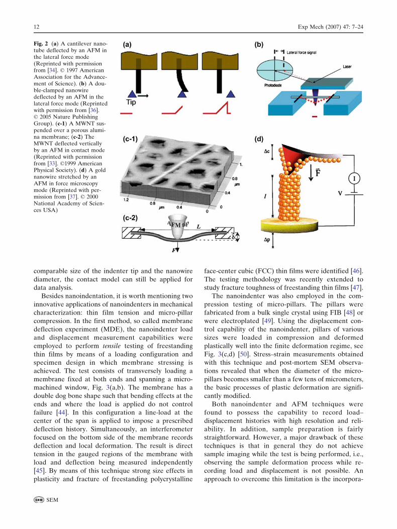
We have also tested MWCNTs in-situ the SEM and
TEM under various electron and ion radiation con-
ditions [55]. The nanotube geometries, radiation con-
ditions and measurement are given in Espinosa et al.
[55]. Figure 8(a) is a plot of load-elongation for the
tested MWCNTs. The plot shows that as the radiation
dose increases, the stiffness of the specimen also
increases. The reason for this stiffness increase under
tensile loading was inferred from the acquired electron
microscopy images. These images revealed that when
MWCNTs are subjected to ion beam radiation (high
radiation dose), the entire cross section breaks, as
shown in Fig. 8(b). By contrast, when MWCNTs are
Fig. 6 In-situ SEM test of a freestanding polysilicon film. (a) Dog-bone shaped tensile test specimen. (b) Magnified view of twoPt displacement markers deposited by EBID. (c) Stress–strain curves of two in-situ SEM tests. Both specimens were 6 mm long and1.6 mm thick. One had a top width of 0.34 mm and a bottom width of 0.87 mm, while the other had a top width of 0.42 mm and a bottomwidth of 1.04 mm. (d) Fracture surface of polysilicon beam showing a mirror region indicative of brittle fracture initiation (Reprintedwith permission from [15]. * 2005 National Academy of Sciences USA)
16 Exp Mech (2007) 47: 7–24
SEM
subjected to e-beam radiation a telescopic failure is
observed with the number of outer shell undergoing
fracture a function of the radiation dose. Multiple shells
fracturing rather than only the outer shell was observed
when the experiment was performed in-situ the TEM at
an operating voltage of 200 kV, see Fig. 8(c). For
experiments conducted in-situ the SEM at an operat-
ing voltage of 5 kV, a single outer shell failure
consistent with previously results reported in the
literature was observed. This suggests that the electron
and ion beam radiation introduces vacancies and
crosslinks between the shells. This is corroborated in
the literature through experimentation and first prin-
ciple calculations [64, 65].
Fig. 7 Images illustrating thenanomanipulation procedureemployed to mount a nano-wire on a NEMS testingsystem. (a) Approach andcontact the nanowire to theMEMS platform. (b) Weldone end of the nanowire usingEBID of Pt gas. (c) Cut theother end using FIB. (d)Weld the other end. (a) and(c) are SEM images, (b) and(d) are FIB images. There is a52- view angle difference be-tween SEM and FIB.(e) Stress–strain curve of a Pdnanowire exhibiting lowerYoung_s modulus and higherstrength than its bulk coun-terpart (Reprinted with per-mission from [15]. * 2005National Academy ofSciences USA)
Exp Mech (2007) 47: 7–24 17
SEM
Another aspect of interest is the stress–strain
behavior of the tested nanostructures so we present
and discuss them in the sequel. Note that in the
process of transforming load–displacement curves into
stress–strain curves, the issue of how to define the tube
cross sectional area arises. In previous in-situ SEM
work, when only the outermost shell carries the load,
the cross section was defined as OD�t (where OD is
the outer diameter of the MWNT and t is the intershell
spacing, about 0.34 nm). However, when crosslinking
between multiple shells exists, a new definition for the
cross sectional area is needed. For this purpose, we
take the in-situ SEM measured modulus (based on
only one shell failure) as the true modulus of the
material and infer the number of failed shells at peak
load by matching the calculated Young_s modulus. For
the CVD grown MWNTs tested in this study, the in-
situ SEM test revealed a Young_s modulus of
315.8T10.8 GPa, which is very similar to the one
reported for arc-grown MWCNT. Figure 9 plots the
stress–strain curves obtained for the tested MWNTs
when subjected to various radiation conditions. The
number of shells used in the calculations is reported in
the same figure. Failure stresses in the range of 12–20
GPa were measured. Note that these stresses are well
below the theoretical stresses predicted for single-
walled nanotubes using quantum and molecular me-
chanics simulations [12]. These authors demonstrate
by means of molecular mechanics calculations that
defects of a few nanometers in size are needed to
explain the measured failure stresses. A distribution of
such defects along the tube length would also explain
the low modulus experimentally measured.
In-situ SEM Electromechanical Testing of a NEMS
Bistable Switch
In addition to the single component testing of CNTs
and NWs, testing of these 1D nanostructures as part of
a NEMS is also needed. For instance, prototype
carbon nanotube based NEMS devices were demon-
strated, such as non-volatile random access memory
elements (NRAM) [66], nanotweezers [67], tunable
oscillator [68], nanorelays [69], and nano-switches [70].
Recently, a cantilever MWCNT-based NEMS device
with close-loop feedback control was developed in our
lab [10]. In this section and as an example of advances
in this area, we will describe such device and present
in-situ SEM experiments suitable for electromechani-
cal characterization.
The device consists of a conductive nanotube
mounted on one electrode (top electrode) as a
cantilever freestanding above another electrode (bot-
tom electrode), Fig. 10(a). A resistor and a power
supply complete the device circuit. When the applied
voltage U<VPI (pull-in voltage), the electrostatic field
acting on the CNT is balanced by the elastic energy
arising from the deformation of the cantilever. The
CNT cantilever remains in an Bupper^ equilibrium
position and the deflection is controlled by the applied
voltage. Above a certain pull-in voltage (the system
becomes unstable) and the CNT accelerates towards
Fig. 8 (a) Load-elongation measurements corresponding toCVD-grown MWCNT specimens tested under various irradia-tion conditions. (b) A typical fracture surface of a MWCNTsubjected to ion beam irradiation showing failure of the entirecross-sectional area. (c) A typical fracture surface of a MWCNTsubjected to e-beam irradiation at 200 kV showing telescopicfailure with multiple-shells broken (Reprinted with permissionfrom [55]. * 2006 Institute of Electrical and ElectronicsEngineers)
18 Exp Mech (2007) 47: 7–24
SEM
the bottom electrode. When the tip of the CNT is very
close to the bottom electrode (e.g., Dõ0.7 nm),
tunneling current flows between the tip-electrode
junction. Due to the existence of the resistor R in the
circuit, the voltage applied to the CNT drops, weak-
ening the electric field. Because of the accumulated
kinetic energy, the CNT continues to move downwards
and the tunneling current increases, weakening the
electric field further. The elastic force becomes larger
than the electrostatic force and the CNT decelerates
and changes its direction of motion. Thus the CNT
becomes arrested and oscillates around a lower
equilibrium position. Due to system damping, the
kinetic energy of the CNT is dissipated and the CNT
stops in this position with stable current in the circuit.
If the applied voltage U decreases, the CNT cantilever
starts retracting. When the voltage U decreases beyond
a certain value, called pull-out voltage, VPO, the CNT
cantilever is released from its lower equilibrium
position and returns back to its upper equilibrium
position. At the same time, the current in the device
diminishes substantially. The pull-in and pull-out
processes form a hysteretic loop in voltage–current
space, Fig. 10(c). The upper and lower equilibrium
positions correspond to BON^ and BOFF^ states,
respectively. The existence of a tunneling current and
the feedback resistor make the Blower^ equilibrium
state very robust, which is essential to some applica-
0
4
8
12
16
20
0 1 2 3 4 5 6
Strain (%)
Str
ess
(GP
a)Test #1 Test #2
Test #3 Test #4
Test #6
Fig. 9 Stress–strain curves for the tested MWNTs. See text fordefinition of cross-sectional area (Reprinted with permissionfrom [55]. * 2006 Institute of Electrical and ElectronicsEngineers)
(a)
Ri > 0
U
CNT
Δ
H r
x
1000
Pull-inPull-out
0 10 20 30 40
100
10
1
0.1
Δ (n
m)
U (volt)
I (A
)
Pull-inPull-out1E-12
1E-10
1E-08
1E-06
0
0 10 20 30 40
U (volt)
(c)(b)
Fig. 10 (a) Schematic of feedback controlled CNT based device with tip tunneling. H is the step height and D is the gap between thedeflected tip and the bottom electrode. Representative characteristic of pull-in and pull-out processes for the feedback-controllednanocantilever device: (b) Relationship between the gap D and the applied voltage U. (c) Relationship between the current i in thecircuit and the applied voltage U. (Reprinted with permission from [10] * 2004, American Institute of Physics)
Exp Mech (2007) 47: 7–24 19
SEM
tions of interest such as switches, random access
memory elements and logic devices. The mathematical
modeling of the device was reported in various
publications [16, 69, 72].
An important activity in novel NEMS development
is the ability to experimentally characterize them. For
the case of the bistable switch described above, we
pursued this endeavor by performing instrumented in-
situ SEM experiments. The employed test configura-
tion is schematically shown in Fig. 11(a) [10, 71]. By
tungsten probe tip by electron beam induced deposi-
tion of platinum. A second electrode employed in the
configuration, Fig. 11(a), consisted of a silicon chip
coated with a 5-nm-thick Cr adhesion layer and a 50 nm
Au film. This chip was glued onto the side of a Teflon
block and vertically mounted in the SEM x–y–z stage.
The Teflon block with the Au electrode was tilted to
meet one of the following testing condition: 1) only the
edge could be viewed under the SEM electron beam
such that the gap between the nanotube cantilever and
the electrode was easily measured; 2) the electrode
surface could be viewed so that the electrode surface
and the mechanical contact between the nanotube and
the electrode could be clearly observed. Using an
electric feedthrough, the two electrodes were connected
to a resistor R=1 GW and to a current–voltage electronic
measurement unit (Keithley 4200 SCS). The nanotube
cantilever welded to the manipulator probe was dis-
placed until a desired distance (typically 0.5õ3 mm,
depending on the length and the diameter of nano-
tubes) between the freestanding CNT and Au electrode
was reached. The pull-in behavior of the device (gap–
voltage curve), in particular, the pull-in voltage, and the
pull-in/pull-out behavior of the device (current–voltage
curve) were examined systematically using this testing
configuration.
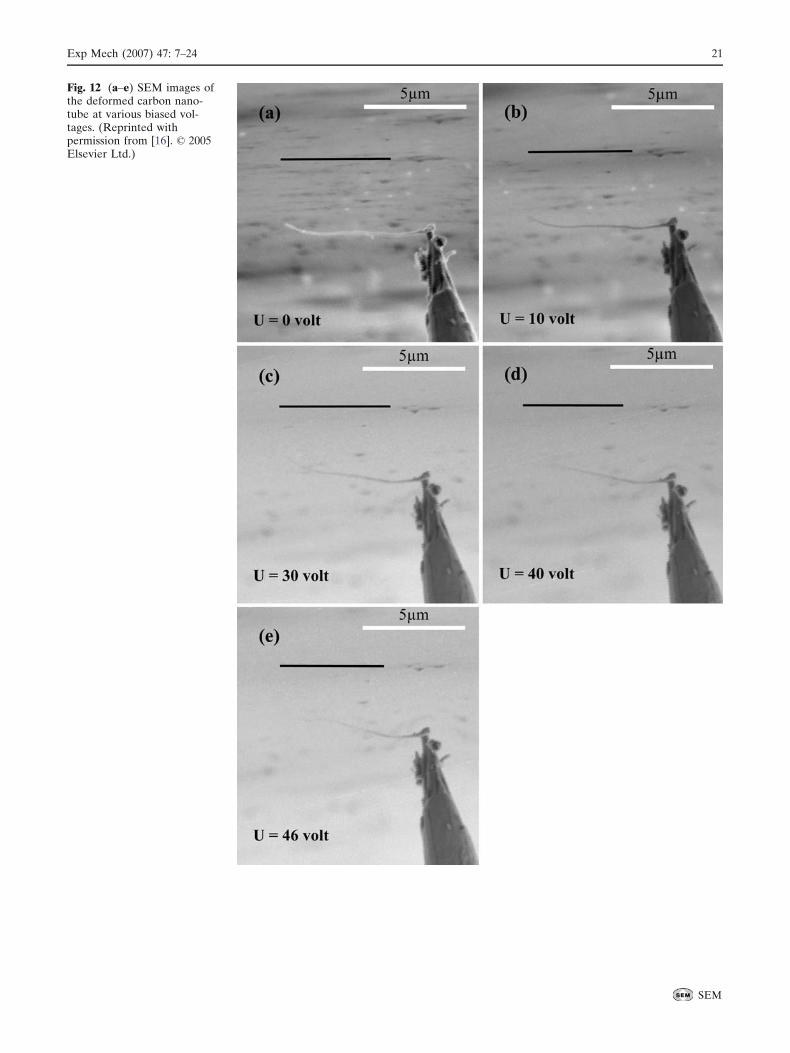
Figure 11(b) shows the measured experimental gap–
voltage (D–U) curve and the theoretical prediction
[72–74], for a multiwalled carbon nanotube cantilever
6.8-mm-long and outer diameter of 47 nm placed
parallel to the electrode with a gap size of 3 mm [16].
Figure 12(a–e) show the SEM images of the deflection
of the carbon nanotube as it was subjected to
increasing applied voltages [16]. A feature on the
electrode, located in the same horizontal plane con-
taining the cantilever nanotube, is schematically
marked as a solid black line in Fig. 12(a–e). Measured
deflections and pull-in voltage, 48 V, were in good
agreement with the theoretical prediction of Vin=47.8
V. Figure 11(c) shows an experimentally measured
current–voltage (I–U) curve during the pull-in/pull-out
processes and the theoretical prediction for a nanotube
Fig. 11 (a) Schematic of the experimental configurationemployed for in-situ SEM electrostatic actuation of MWNTs.(b) Measured D–V characteristic curve during pull-in process andcomparison with analytical predictions. (Reprinted with permis-sion from [16]. * 2005 Elsevier Ltd.) (c) Measured I–Vcharacteristic curve during the pull-in/pull-out processes andcomparison with analytical predictions. The arrows show thedirection in which the hysteretic loop is described during theincrease and decrease of the driving voltage U (Reprinted withpermission from [71]. * 2006 WILEY-VCH Verlag GmbH andCo, KGaA Weinheim)
20 Exp Mech (2007) 47: 7–24
SEM
Fig. 12 (a–e) SEM images ofthe deformed carbon nano-tube at various biased vol-tages. (Reprinted withpermission from [16]. * 2005Elsevier Ltd.)
Exp Mech (2007) 47: 7–24 21
SEM
9-mm-long [71]. The measured I–U curve exhibited the
theoretically predicted bi-stability and hysteretic loop.
The arrows show the direction in which the hysteretic
loop was traveled during the increase and decrease of
the driving voltage U. The measurement exhibits a
background noise of about 0.1 pA, which is typical in
these measurements.
It is worth mentioning that the aforementioned in-
situ electro-mechanical SEM testing methodology is
generic and as such it can be advantageously employed
to investigate other types of nanotube- or nanowire-
based nanoelectromechanical devices.
Concluding Remarks
In this article we reviewed recently developed exper-
imental techniques for the mechanical characterization
of 1D nanostructures of particular relevance to emerg-
ing MEMS and NEMS technologies. It was highlighted
that: 1) a variety of methods have been developed to
facilitate the manipulation and positioning of 1D
nanostructures; 2) nanoindenter and especially AFM
have become indispensable tools for nanomechanical
testing due to their extraordinarily high load and
displacement resolution; 3) an effort has been made
in developing MEMS based testing apparatuses, which
can be easily placed inside AFMs, SEMs and TEMs,
such that continuous imaging of the specimen can be
pursued at high magnifications while electronically and
independently measuring load.
Unfortunately, but perhaps not surprisingly, the
data from nanomechanical measurements are often
contradictory. For example, the Young_s modulus of
CNTs was reported to be between 0.1 to more than
1 TPa. In this review we have provided some insight
into possible sources leading to such inconsistency. Dif-
ferent material fabrication methods may lead to differ-
ent atomic defect sizes and types. Moreover, different
nanomechanical testing techniques, from bending to
uniaxial tension configurations with and without real
time electron beam imaging, possess a range of reso-
lutions. These findings demonstrate that there is a high
need for the development of standardized metrology
techniques. In this regard, we have described a novel
nanoscale material testing system based on MEMS
technology, [15, 54] which may serve as a baseline
example. Such approach seems promising and could
be extended to a variety of electro-thermal-mechanical
characterization configurations. In this regard, a major
challenge has been identified, which is the manipulation
and positioning of individual nanostructures onto the
nanoscale testing systems. The feasibility of this task by
mounting and welding individual nanowires and CNTs
onto MEMS testing devices was demonstrated [15].
However, the procedure is quite time consuming and
gives low yield. Other approaches consisting of direct
synthesis of 1D nanostructures on the testing system
should be pursued. An example in this direction is the
growth of silicon nanowires between two existing elec-
trodes [32]. New synthesis methods should also be
investigated to directly synthesize metallic and other
nanowires.
While here we have focused on the characterization
of mechanical properties, it is recognized that electro-
mechanical-thermal characterization is equally impor-
tant due to the multifunctional features of nanodevices.
In this regard, both experimentation and multiscale
analysis of the electro-mechanical-thermal behavior
under device operational conditions needs to be pur-
sued. Such endeavor is quite challenging but at the same
time scientifically stimulating. An example involving
the in-situ SEM testing of a CNT-based NEMS was
demonstrated. Nonetheless, such testing is just in its
infancy. Another area that requires particular atten-
tion is the scaling up of device nanofabrication to two
dimensional arrays. Approaches involving the directed
self-assembly of CNTs and NWs seems promising in
this respect [32] and should be further investigated.
Finally, key to the future of nanomechanics will be
direct comparison between nanomechanical experiments
and multiscale simulations of the tested nanostructures.
Quantum mechanics and atomistic simulations have
been able to predict unique nanomechanical behaviors
but they are based on various types of approximations.
Hence, the predicted capability of theoretical predictions
needs to be assessed by experimentation. With further
advances in nanomechanical testing techniques and real
time high atomic resolution observations, the source of
defects, their nucleation, interaction and evolution will
become more quantitative. In turn advances in multi-
scale modeling will make possible a combined experi-
mental–computational approach clearly required to
make further advances in nanoscale material science
and its applications.
Acknowledgments The authors acknowledge the support fromthe FAA through Award No. DTFA03-01-C-00031, AROthrough Award No. W911NF-05-1-0088, and the NSF throughawards No. CMS-0120866, DMR-0315561. Work was alsosupported in part by the Nanoscale Science and EngineeringInitiative of the National Science Foundation under NSF AwardNumber EEC-0118025. SEM calibration and testing wereperformed at the EPIC facility of NUANCE center at North-western University. Nanomanipulation was carried out in theCenter for Microanalysis of Materials, University of Illinois,which is partially supported by the U.S. Department of Energy
22 Exp Mech (2007) 47: 7–24
SEM
under grant DEFG02-96-ER45439. We thank I. Petrov, J.Mabon and M. Marshall for many useful discussions and forfacilitating the microscopy work reported in this manuscript.
References
1. Iijima S (1991) Helical microtubules of graphitic carbon.Nature 354(6348):56–58.
2. Xia YN, Yang PD, Sun YG, Wu YY, Mayers B, Gates B,Yin YD, Kim F, Yan YQ (2003) One-dimensional nano-structures: Synthesis, characterization, and applications. AdvMater 15(5):353–389.
3. Ke CH, Espinosa HD (2006) Nanoelectromechanical Sys-tems (NEMS) and modeling. Handbook of Theoretical andComputational Nanotechnology. American Scientific Pub-lishers.
4. Yu MF, Lourie O, Dyer MJ, Moloni K, Kelly TF, Ruoff RS(2000) Strength and breaking mechanism of multiwalled carbonnanotubes under tensile load. Science 287(5453):637–640.
5. Wildoer JWG, Venema LC, Rinzler AG, Smalley RE,Dekker C (1998) Electronic structure of atomically resolvedcarbon nanotubes. Nature 391(6662):59–62.
6. Li DY, Wu YY, Kim P, Shi L, Yang PD, Majumdar A (2003)Thermal conductivity of individual silicon nanowires. ApplPhys Lett 83(14):2934–2936.
7. Duan XF, Huang Y, Agarwal R, Lieber CM (2003) Single-nanowire electrically driven lasers. Nature 421(6920):241–245.
8. Dalton AB, Collins S, Munoz E, Razal JM, Ebron VH,Ferraris JP, Coleman JN, Kim BG, Baughman RH (2003)Super-tough carbon-nanotube fibres — These extraordinarycomposite fibres can be woven into electronic textiles.Nature 423(6941):703.
9. Fennimore AM, Yuzvinsky TD, Han WQ, Fuhrer MS,Cumings J, Zettl A (2003) Rotational actuators based oncarbon nanotubes. Nature 424(6947):408–410.
10. Ke CH, Espinosa HD (2004) Feedback controlled nano-cantilever device. Appl Phys Lett 85(4):681–683.
11. Cui Y, Wei QQ, Park HK, Lieber CM (2001) Nanowire nano-sensors for highly sensitive and selective detection of biolog-ical and chemical species. Science 293(5533):1289–1292.
12. Zhang SL, Mielke SL, Khare R, Troya D, Ruoff RS, SchatzGC, Belytschko T (2005) Mechanics of defects in carbonnanotubes: Atomistic and multiscale simulations. Phys RevB 71(11).
13. Gall K, Diao JK, Dunn ML (2004) The strength of goldnanowires. Nano Lett 4(12):2431–2436.
14. Haque MA, Saif MTA (2004) Deformation mechanisms infree-standing nanoscale thin films: A quantitative in situtransmission electron microscope study. Proc Natl Acad SciUSA 101(17):6335–6340.
15. Zhu Y, Espinosa HD (2005) An electromechanical materialtesting system for in situ electron microscopy and applica-tions. Proc Natl Acad Sci USA 102(41):14503–14508.
16. Ke CH, Pugno N, Peng B, Espinosa HD (2005) Experimentsand modeling of carbon nanotube-based NEMS devices. JMech Phys Solids 53(6):1314–1333.
17. Falvo MR, Clary GJ, Taylor RM, Chi V, Brooks FP, WashburnS, Superfine R (1997) Bending and buckling of carbon nano-tubes under large strain. Nature 389(6651):582–584.
18. Williams PA, Papadakis SJ, Falvo MR, Patel AM, SinclairM, Seeger A, Helser A, Taylor RM, Washburn S, SuperfineR (2002) Controlled placement of an individual carbonnanotube onto a microelectromechanical structure. ApplPhys Lett 80(14):2574–2576.
19. Poncharal P, Wang ZL, Ugarte D, de Heer WA (1999)Electrostatic deflections and electromechanical resonancesof carbon nanotubes. Science 283(5407):1513–1516.
20. Cumings J, Zettl A (2000) Low-friction nanoscale linearbearing realized from multiwall carbon nanotubes. Science289(5479):602–604.
21. Smith PA, Nordquist CD, Jackson TN, Mayer TS, MartinBR, Mbindyo J, Mallouk TE (2000) Electric-field assistedassembly and alignment of metallic nanowires. Appl PhysLett 77(9):1399–1401.
22. Chen XQ, Saito T, Yamada H, Matsushige K (2001)Aligning single-wall carbon nanotubes with an alternating-current electric field. Appl Phys Lett 78(23):3714–3716.
23. Chung J, Lee J (2003) Nanoscale gap fabrication andintegration of carbon nanotubes by micromachining. SensActuators A-Phys 104(3):229–235.
24. Hughes MP, Morgan H (1998) Dielectrophoretic trapping ofsingle sub-micrometre scale bioparticles. J Phys D Appl Phys31(17):2205–2210.
25. Huang Y, Duan XF, Wei QQ, Lieber CM (2001) Directedassembly of one-dimensional nanostructures into functionalnetworks. Science 291(5504):630–633.
26. Fujiwara M, Oki E, Hamada M, Tanimoto Y, Mukouda I,Shimomura Y (2001) Magnetic orientation and magneticproperties of a single carbon nanotube. J Phys Chem A105(18):4383–4386.
27. Rao SG, Huang L, Setyawan W, Hong SH (2003) Large-scaleassembly of carbon nanotubes. Nature 425(6953):36–37.
28. Piner RD, Zhu J, Xu F, Hong SH, Mirkin CA (1999) BDip-pen^ nanolithography. Science 283(5402):661–663.
29. Kim KH, Moldovan N, Espinosa HD (2005) A nanofountainprobe with sub-100 nm molecular writing resolution. Small1(6):632–635.
30. Dai HJ (2000) Controlling nanotube growth. Physics World13(6):43–47.
31. Kong J, Soh HT, Cassell AM, Quate CF, Dai HJ (1998)Synthesis of individual single-walled carbon nanotubes onpatterned silicon wafers. Nature 395(6705):878–881.
32. He RR, Gao D, Fan R, Hochbaum AI, Carraro C, MaboudianR, Yang PD (2005) Si nanowire bridges in microtrenches:Integration of growth into device fabrication. Adv Mater 17(17):2098–+.
33. Salvetat JP, Briggs GAD, Bonard JM, Bacsa RR, Kulik AJ,Stockli T, Burnham NA, Forro L (1999) Elastic and shearmoduli of single-walled carbon nanotube ropes. Phys RevLett 82(5):944–947.
34. Wong EW, Sheehan PE, Lieber CM (1997) Nanobeammechanics: Elasticity, strength, and toughness of nanorodsand nanotubes. Science 277(5334):1971–1975.
35. Walters DA, Ericson LM, Casavant MJ, Liu J, Colbert DT,Smith KA, Smalley RE (1999) Elastic strain of freelysuspended single-wall carbon nanotube ropes. Appl PhysLett 74(25):3803–3805.
36. Wu B, Heidelberg A, Boland JJ (2005) Mechanical propertiesof ultrahigh-strength gold nanowires. Nat Mat 4(7):525–529.
37. Marszalek PE, Greenleaf WJ, Li HB, Oberhauser AF,Fernandez JM (2000) Atomic force microscopy capturesquantized plastic deformation in gold nanowires. Proc NatlAcad Sci USA 97(12):6282–6286.
38. Marszalek PE, Li HB, Oberhauser AF, Fernandez JM (2002)Chair–boat transitions in single polysaccharide moleculesobserved with force-ramp AFM. Proc Natl Acad Sci USA99(7):4278–4283.
39. Rief M, Gautel M, Oesterhelt F, Fernandez JM, Gaub HE(1997) Reversible unfolding of individual titin immunoglob-ulin domains by AFM. Science 276(5315):1109–1112.
Exp Mech (2007) 47: 7–24 23
SEM
40. Tan EPS, Goh CN, Sow CH, Lim CT (2005) Tensile test of asingle nanofiber using an atomic force microscope tip. ApplPhys Lett 86(7).
41. Li XD, Hao HS, Murphy CJ, Caswell KK (2003) Nano-indentation of silver nanowires. Nano Lett 3(11):1495–1498.
42. Feng G, Nix WD, Yoon Y, Lee CJ (2006) A study of themechanical properties of nanowires using nanoindentation. JAppl Phys 99(7).
43. Waters JF, Guduru PR, Jouzi M, Xu JM, Hanlon T, Suresh S(2005) Shell buckling of individual multiwalled carbonnanotubes using nanoindentation. Appl Phys Lett 87(10).
44. Pugno N, Peng B, Espinosa HD (2005) Predictions of strengthin MEMS components with defects —A novel experimental–theoretical approach. Int J Solids Struct 42(2):647–661.
45. Espinosa HD, Prorok BC, Fischer M (2003) A methodol-ogy for determining mechanical properties of freestandingthin films and MEMS materials. J Mech Phys Solids51(1):47–67.
46. Espinosa HD, Prorok BC, Peng B (2004) Plasticity sizeeffects in free-standing submicron polycrystalline FCC filmssubjected to pure tension. J Mech Phys Solids 52(3):667–689.
47. Espinosa HD, Peng B (2005) A new methodology toinvestigate fracture toughness of freestanding MEMS andadvanced materials in thin film form. J MicroelectromechSys 14(1):153–159.
49. Greer JR, Oliver WC, Nix WD (2005) Size dependence ofmechanical properties of gold at the micron scale in theabsence of strain gradients. Acta Mater 53(6):1821–1830.
50. Zhang H, Schuster BE, Wei Q, Ramesh KT (2006) Thedesign of accurate micro-compression experiments. ScrMater 54(2):181–186.
51. Cheng S, Spencer JA, Milligan WW (2003) Strength andtension/compression asymmetry in nanostructured and ultra-fine-grain metals. Acta Mater 51(15):4505–4518.
52. Legros M, Dehm G, Balk TJ, Arzt E, Bostrom O, GergaudP, Thomas O, Kaouache B (2003) Material Sciences SocietySymposium Proceedings.
53. Minor AM, Morris JW, Stach EA (2001) Quantitative in situnanoindentation in an electron microscope. Appl Phys Lett79(11):1625–1627.
54. Zhu Y, Moldovan N, Espinosa HD (2005) A microelectrome-chanical load sensor for in situ electron and x-ray microscopytensile testing of nanostructures. Appl Phys Lett 86(1).
55. Espinosa HD, ZhuY, Moldovan N (2005) Design andoperation of a MEMS-based material testing system for in-situ electron microscopy testing of nanostructures. Acceptedby Journal of Microelectromechanical Systems.
56. Zhu Y, Corigliano A, Espinosa HD (2006) A thermalactuator for nanoscale in-situ microscopy testing: Designand characterization. J Micromech Microeng 16(2):242–253.
60. Greek S, Ericson F, Johansson S, Furtsch M, Rump A (1999)Mechanical characterization of thick polysilicon films:Young_s modulus and fracture strength evaluated withmicrostructures. J Micromech Microeng 9(3):245–251.
61. Sharpe WN, Jackson KM, Hemker KJ, Xie ZL (2001) Effectof specimen size on Young_s modulus and fracture strengthof polysilicon. J Microelectromech Sys 10(3):317–326.
62. Tsuchiya T, Tabata O, Sakata J, Taga Y (1998) Specimen sizeeffect of tensile strength of surface-micromachined polycrys-talline silicon thin films. J Microelectromech Sys 7(1): 106–113.
63. Espinosa HD, Berbenni S, Panico M, Schwarz KW (2005)An interpretation of size-scale plasticity in geometricallyconfined systems. Proc Natl Acad Sci USA 102(47):16933–16938.
64. Huhtala M, Krasheninnikov AV, Aittoniemi J, Stuart SJ,Nordlund K, Kaski K (2004) Improved mechanical loadtransfer between shells of multiwalled carbon nanotubes.Phys Rev B 70(4).
65. Kis A, Csanyi G, Salvetat JP, Lee TN, Couteau E, Kulik AJ,Benoit W, Brugger J, Forro L (2004) Reinforcement ofsingle-walled carbon nanotube bundles by intertube bridg-ing. Nat Mat 3(3):153–157.
66. Rueckes T, Kim K, Joselevich E, Tseng GY, Cheung CL,Lieber CM (2000) Carbon nanotube-based nonvolatilerandom access memory for molecular computing. Science289(5476):94–97.
67. Kim P, Lieber CM (1999) Nanotube nanotweezers. Science286(5447):2148–2150.
69. Kinaret JM, Nord T, Viefers S (2003) A carbon-nanotube-based nanorelay. Appl Phys Lett 82(8):1287–1289.
70. Jang JE, Cha SN, Choi Y, Amaratunga GAJ, Kang DJ,Hasko DG, Jung JE, Kim JM (2005) Nanoelectromechanicalswitches with vertically aligned carbon nanotubes. Appl PhysLett 87(16).
71. Ke CH, Espinosa HD (2006) In-situ Electron MicroscopyElectro-Mechanical Characterization of a NEMS BistableDevice, Small 2(12):1484–1489.
72. Dequesnes M, Rotkin SV, Aluru NR (2002) Calculation ofpull-in voltages for carbon-nanotube-based nanoelectrome-chanical switches. Nanotechnology 13(1):120–131.
73. Ke CH, Espinosa HD, Pugno N (2005) Numerical analysis ofnanotube based NEMS devices —Part II: Role of finitekinematics, stretching and charge concentrations. TransASME-J App Mech 72(5):726–731.
74. Ke CH, Espinosa HD (2005) Numerical analysis of nano-tube-based NEMS devices —Part I: Electrostatic chargedistribution on multiwalled nanotubes. Trans ASME-J AppMech 72(5):721–725.


![Investigation of mechanical degradation mechanism onto the ......[1] Jack W. Ekin, Experimental Techniques for Low-Temperature Measurements : Cryostat Design, Material Properties,](https://static.documents.pub/doc/80x56/5f0442b77e708231d40d19b1/investigation-of-mechanical-degradation-mechanism-onto-the-1-jack-w-ekin.jpg)


