+ All Categories
Home > Documents > Exploration of Novel Tunnel Barrier Materials for STT-RAM · Exploration of Novel Tunnel Barrier...

Exploration of Novel Tunnel Barrier Materials for STT-RAM · Exploration of Novel Tunnel Barrier...

Date post: 27-May-2018
Category:
Upload: hoangdiep
View: 219 times
Download: 0 times
Share this document with a friend
30
Exploration of Novel Tunnel Barrier Materials for STT-RAM Wei Chen Wei Chen Condensed Matter Seminar 04/24/08 1 Wei Chen Advisor: Dr. Stuart Wolf Department of Physics University of Virginia Funded by DARPA and DMEA Collaborator: NIST, Freescale
Transcript

Exploration of Novel Tunnel Barrier Materials for STT-RAM

Wei Chen

Wei Chen Condensed Matter Seminar 04/24/081

Wei Chen Advisor: Dr. Stuart Wolf

Department of PhysicsUniversity of Virginia

Funded by DARPA and DMEACollaborator: NIST, Freescale

Outline

• Introduction and Motivation• Background Theory• Experiment Setups

Wei Chen Condensed Matter Seminar 04/24/082

• Experiment Setups• Results & Discussion• Summary & Future Plan

Outline

• Introduction and Motivation• What is Magnetic Tunnel Junction (MTJ)?• MRAM: Major Application of MTJ• New Solution: Spin Torque Transfer!

Wei Chen Condensed Matter Seminar 04/24/083

• New Solution: Spin Torque Transfer!

• Background Theory• Experiment Setups• Results & Discussion• Summary & Future Plan

Magnetic Tunnel Junction

AFM

Pinned FM

Tunnel Barrier

Free FM

Wei Chen Condensed Matter Seminar 04/24/084

[Spintronics Class Lecture Notes, Stuart Wolf, Spring 2007]

Basic Structure of Exchange Biased MTJ

Free FM

Substrate

MRAM: Major Application of MTJ

Wei Chen Condensed Matter Seminar 04/24/085

[Spintronics Class Lecture Notes, Stuart Wolf, Spring 2007]

Potential Advantages:• Compatibility with CMOS• Density and speed of DRAM • Less power than FLASH

Main Challenges:

MRAM: Major Application of MTJ

Field Switching MRAM cannot be effectively scaled down (65nm node)!

Wei Chen Condensed Matter Seminar 04/24/086

• Less power than FLASH• Unlimited writing cycles• Truly Non-volatile

u

B

K V

k T

• 1T-1MTJ cell structure limited by the size of transistor!• Thermal Stability Factor:

down (65nm node)!

Spin Torque Transfer Switching

Key Advantage compared with conventional field switching: • Highly Scalablewriting

Wei Chen Condensed Matter Seminar 04/24/087

• A spin-polarized current injected into a ferromagnetic layer can induce a torque on its magnetization, hence rotate the magnetization.

• Highly Scalablewriting current scales down with cell size with constant Jc!

Key Advantages and Potentials of STTRAM

Wei Chen Condensed Matter Seminar 04/24/088

• Excellent write selectivity ~ localized spin-injection within cell

• Highly Scalable ~ write current scales down with cell size

• Low power ~ low write current

• Simpler Architecture ~ no write lines, no bypass line and no cladding

• High Speed ~ Few nanoseconds

=> Too high to be practical! ( )

Spin Torque Transfer Switching

ηπδα

h

MHeMJ ss

c

)2(2 +=

0.1) kA/m, 1420 ,5.2:(Co A/cm10~ 28 === αδ sc MnmJ

Model by Slonczewski:

26 /10 cmA

Wei Chen Condensed Matter Seminar 04/24/089

=> Too high to be practical! ( )26 /10 cmA

What we could engineer:•Ms Saturation Magnetization Decrease• α Gilbert damping parameter Decrease• η Spin Transfer Efficiency Increase

Novel Barrier Exploration

• Only ~70% with AlOx-MTJs.• TMR record with MgO barrier: Over 300%! MgO increases η (spin transfer efficiency) significantly!

Wei Chen Condensed Matter Seminar 04/24/0810

significantly!

New Barriers Exploration Increase η :• Oxides: VOx, TiOx, TaOx• Nitrides: BN

• prevent the oxidation of under layer FM

• large gap provides robust tunneling

Smart Barrier for MTJsChallenge for SMT-MTJs:High Jc “Writing” voltage very close to junction break down voltage

VO2: • Structural phase transformation from Monoclinic to Rutile at ~340K • Current Driven transition

10-1

100

Monoclinic Rutile Read in high R phase for highest MR%

Wei Chen Condensed Matter Seminar 04/24/0811

280 320 360 40010-4

10-3

10-2

10

ρρ ρρ (Ω

·cm

)

T (K)

Transition temperature: ~ 340 K

[Work by Kevin West]

for highest MR%

Write in low R phasefor lowest power!

Outline

• Introduction and Motivation• Background Theory

• Spin-dependent Transport• Spin Polarized Electron Tunneling: FM-I-FM

Wei Chen Condensed Matter Seminar 04/24/0812

• Spin Polarized Electron Tunneling: FM-I-FM• AFM/FM Exchange Bias

• Experiment Setups• Results & Discussion• Summary & Future Plan

Spin-dependent Transport

Wei Chen Condensed Matter Seminar 04/24/0813

Density of State diagram for ferromagnetic metal: g↑ > g↓

[Spintronics Class Lecture Notes, Stuart Wolf, Spring 2007][Mark Jonson, J. Phys. Chem. B (2005), 109, 14278-14291]

current through ferromagnetic metal

Spin Polarized Electron Tunneling: FM-I-FM

Julliere’s model:• spin conserved tunneling•

↑↓↓↑

↓↓↑↑

+=

+=

2121

2121

NNNNG

NNNNG

AP

p

Wei Chen Condensed Matter Seminar 04/24/0814

21

21

1

2

PP

PP

G

GG

R

RR

R

RTMR

Ap

APp

P

PAP

P −=

−=−=∆=

↓↑

↓↑

↓↑

↓↑

+−

=

+−

=

22

222

11

111

NN

NNP

NN

NNP

Exchange Bias

Wei Chen Condensed Matter Seminar 04/24/0815

[J.Nogues, Ivan Schuller, JMMM192(1999) 203-232]

FMFM

AFMFMexEB tMa

SSJH 2

2=

Outline

• Introduction and Motivation• Background Theory• Experiment Setups

Wei Chen Condensed Matter Seminar 04/24/0816

• Experiment Setups• Reactive Biased Target Ion Beam Deposition• Lithographic patterning process• CIPTech Measurement

• Results & Discussion• Summary & Future Plan

Reactive Biased Target Ion Beam Deposition

Wei Chen Condensed Matter Seminar 04/24/0817

• Low Energy Ion Source (5-50eV)

• High Temperature ~ 700 °C

• Smooth Surface/Interface Layer

• Control Phase Formation

• Combinatorial Growth Complex Oxides

Lithographic Patterning (I)

Unpatterned MTJ Film (Cross-section View)

• i) Apply mask, develop photo resister (PR)• ii) Dry etching to define junction structure; leave PR for next-step lift-off process

Wei Chen Condensed Matter Seminar 04/24/0818

Cross-section View Plane View

lift-off process

i) ii)

Lithographic Patterning (II)

• iii) Deposition of ~ 300nm SiO2 by rf-sputtering as passivation layer• iv) Dissolve PR in Acetone to finish lift-off process• v) Apply and develop another

iii)

Wei Chen Condensed Matter Seminar 04/24/0819

• v) Apply and develop another layer of mask, deposit and define Ti/Au contact layer by lift-off

iv)

v)

Cross-section View

Plane View

Top Contacts

Bottom Contacts

CIPTech Measurement

• Fast, nondestructive, and accurateway to measure TMR without patterning!• Collaboration with NIST

Wei Chen Condensed Matter Seminar 04/24/0820

D. C. Worledge, etc. APL, 83, 84 (2003)

Outline

• Introduction and Motivation• Background Theory• Experiment Setups

Wei Chen Condensed Matter Seminar 04/24/0821

• Experiment Setups• Results & Discussion• Summary & Future Plan

MTJ with AlOx Barrier (I)

15nm Ta

6nm CoFeB

~1nm AlOx

0

100

200

M(m

icro

em

u)

Wei Chen Condensed Matter Seminar 04/24/0822

~1nm AlOx

5nm Ta3nm CoFeB

Si/SiO2 Substrate

-50 -40 -30 -20 -10 0 10 20 30 40 50

-200

-100M(m

icro

em

u)

H(Oe)

Black: 1SccmO2 5min Oxidation

Blue: 5SccmO2 2mins Oxidation

Red: 5SccmO2 4mins Oxidation

Better oxidized AlOx barrier provides better separated switching!

AlOx-MTJ Stack

MTJ with AlOx Barrier (II)

8.2279

8.2280

8.2281

8.2282

8.2283

Res

ista

nce

(oh

m)

TMR Measurement of MJT Unit @ 5K

Wei Chen Condensed Matter Seminar 04/24/0823

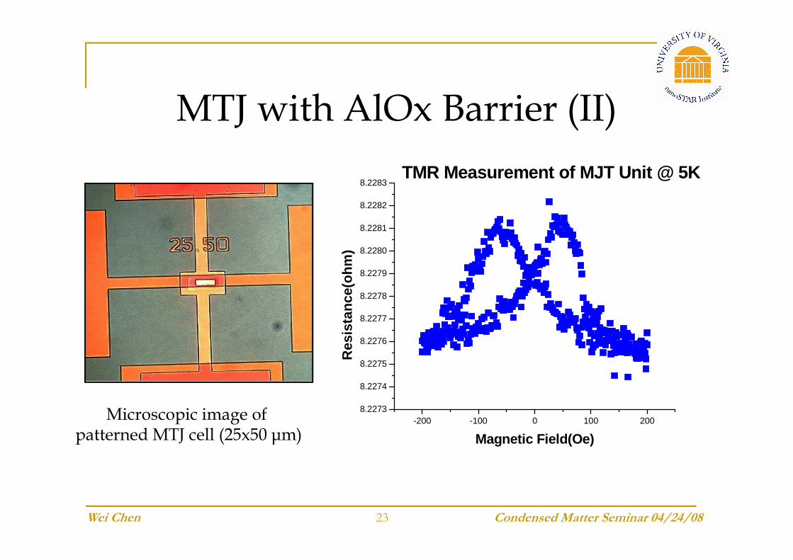
Microscopic image of patterned MTJ cell (25x50 µm)

-200 -100 0 100 2008.2273

8.2274

8.2275

8.2276

8.2277

8.2278

Res

ista

nce

(oh

m)

Magnetic Field(Oe)

Ar/O2 Flow Rate (Sccm) Resistance (Ohm) Change

(RT->~100C)

5.5 200K->30K

• Growth condition: on top of sub/CoFeB(1nm)/V(0.5nm)• VOx thickness: ~50nm

VOx Recipe Development

Wei Chen Condensed Matter Seminar 04/24/0824

5.5 200K->30K

6 680K->150K

6.5 2,500K->400K

7 Too insulating

6 (with enhanced ion energy~50eV)

57K Ohm->200 Ohm (Temperature:50K->250K )

IrMn/CoFeB Exchange Bias

50

100

Mo

men

t (m

icro

em

u)

15nm Ru

10nm IrMn(AFM)

5nm CoFeB (FM) Exchange Bias

Wei Chen Condensed Matter Seminar 04/24/0825

-600 -400 -200 0 200 400 600

-100

-50

0

Mo

men

t (m

icro

em

u)

H(Oe)

20nm Ru

5nm Ta

Si/SiO2 Substrate

10nm IrMn(AFM) Exchange Bias

Hex ~ 250 Oe

MTJ with VOx Barrier (I)

50

100

150

M (

mic

ro e

mu

)

M vs H @ 305K

10nm Ru

5nm CoFeB (FM)

5nm CoFeB (FM)5nm Ta

1~2nm VOx

Pinned Layer

Free Layer Tunnel Barrier

Wei Chen Condensed Matter Seminar 04/24/0826

-600 -400 -200 0 200 400 600-150

-100

-50

0

M (

mic

ro e

mu

)

H (Oe)

***The sample is measured after annealing in forming gas(95%Ar 5%H2) at 250C, 4kOe for 1hr

20nm Ru

5nm Ta

Si/SiO2 Substrate

10nm IrMn(AFM)

5nm CoFeB ( )Pinned Layer

VOx-MTJ Stack

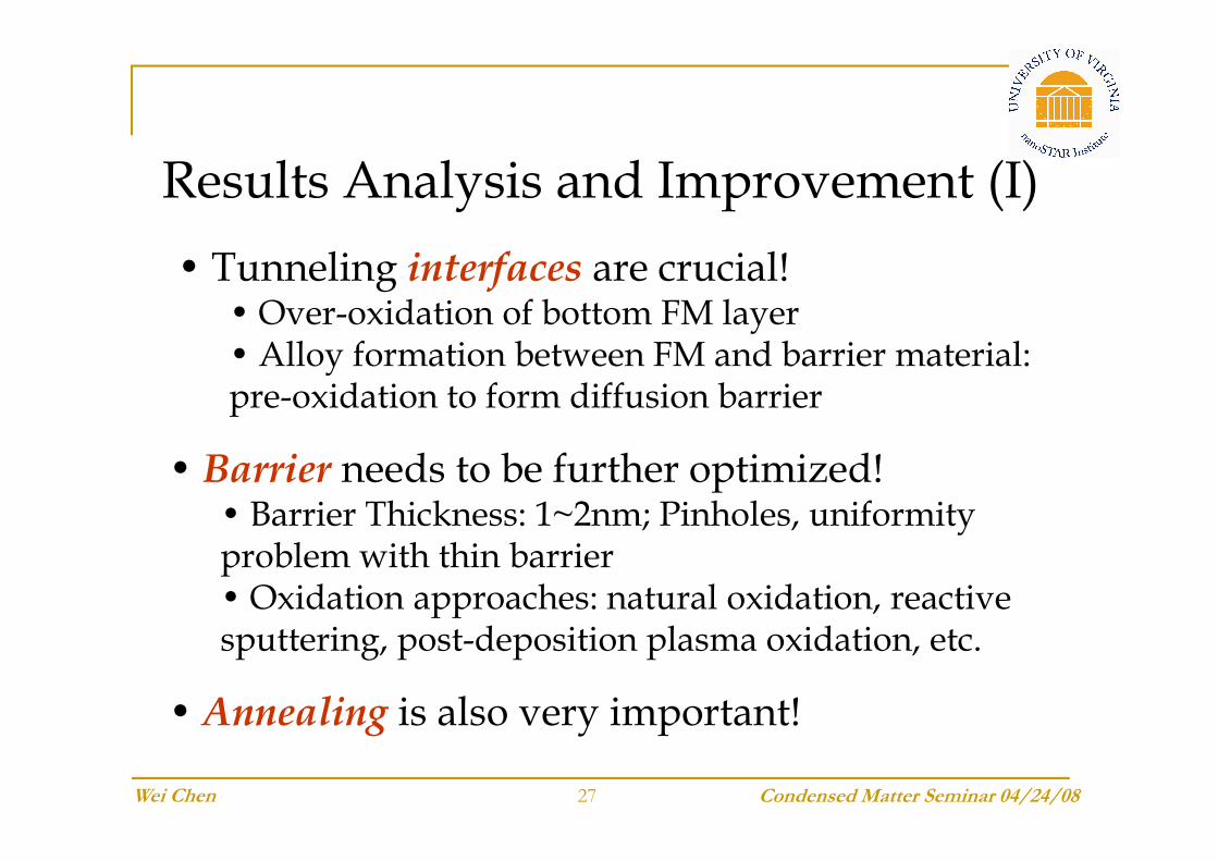
Results Analysis and Improvement (I)

• Tunneling interfaces are crucial!• Over-oxidation of bottom FM layer • Alloy formation between FM and barrier material: pre-oxidation to form diffusion barrier

Wei Chen Condensed Matter Seminar 04/24/0827

• Barrier needs to be further optimized!• Barrier Thickness: 1~2nm; Pinholes, uniformity problem with thin barrier• Oxidation approaches: natural oxidation, reactive sputtering, post-deposition plasma oxidation, etc.

• Annealing is also very important!

Results Analysis and Improvement (II)

Dry etching is crucial in defining MTJ unit, and it could be further optimization!Solutions:

Wei Chen Condensed Matter Seminar 04/24/0828

Solutions:• Using tilted rotating stage• Reactive Etching Ar+Cl2

Utilizing more tools to facilitate the lithographic processing:AFM, SEM, EBL, etc.

Summary

• Growth of Prototype AlOx-MTJ

• Development of Basic Patterning Process

Wei Chen Condensed Matter Seminar 04/24/0829

• Development of Basic Patterning Process

• VOx Material Exploration

• Preliminary VOx-MTJ Experiments

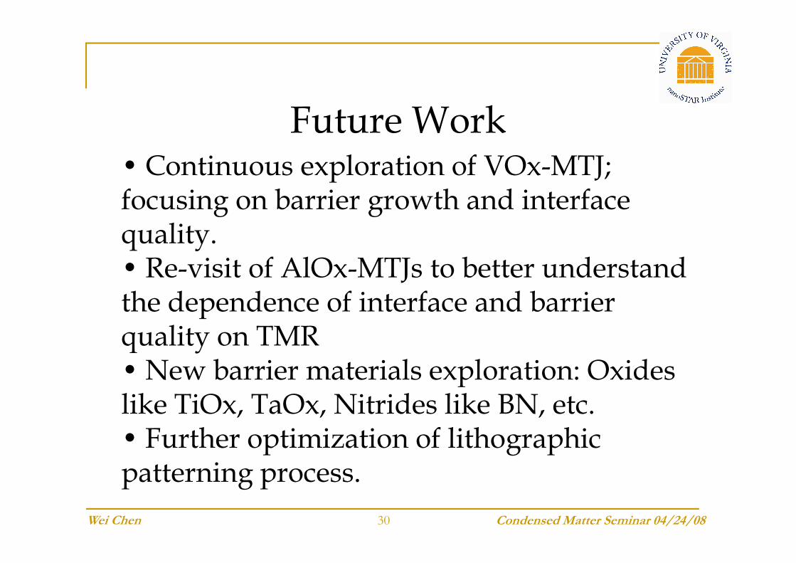
Future Work• Continuous exploration of VOx-MTJ; focusing on barrier growth and interface quality.• Re-visit of AlOx-MTJs to better understand

Wei Chen Condensed Matter Seminar 04/24/0830

• Re-visit of AlOx-MTJs to better understand the dependence of interface and barrier quality on TMR• New barrier materials exploration: Oxides like TiOx, TaOx, Nitrides like BN, etc. • Further optimization of lithographic patterning process.


Recommended