J. Instrum. Soc. India 32 (4) 239 - 247 EXTERNAL DEVICE CONTROL USING IBM PC’s CENTRONICS PRINTER PORT P. Thimmaiah, K.R. Rao and E.R. Gopal Department of Physics and Electronics, Sri Krishnadevaraya University Anantapur - 515 003, Andhra Pradesh ABSTRACT IBM PCs with parallel printer ports are widely available in teaching and research laboratories. This paper describes a novel system for controlling any equipment in general, positioning with stepping motors in particular via the parallel Centronics printer port of an IBM PC or compatible. Techniques are presented for exploring the unused parallel port or exploiting the Centronics printer port for control. Programs are developed for position control of stepper motor using Macro Assembler MASM 86. 1. INTRODUCTION Personal computers (PCs) are widely used in research and development laboratories and teaching laboratories for software development and analysis purposes. PCs can also be used in measurement and control of outside world devices. This method of controlling the external device by connecting it to the PC is known as interfacing. PC interfacing with the outside world calls for extra hardware in the form of plug-in-cards 1,2 . These cards which are popularly known as IEEE/GPIB data acquisition cards and digital input-output timer (DIOT) cards are available on the market. These cards can be purchased and inserted in the plug-and-play ISA sockets of the PC mother board and can be interfaced with the outside device. These cards are costly and difficult to mount inside the PC because the cabinet of the PC has to be removed for mounting the card on the PC mother board and correct base address which doesn’t clash with hardware resources of the PC has to be chosen. Recent IBM PC compatible mother boards doesn’t provide ISA socket, unless otherwise requested for. Further, the present standard PCI compatible data acquisition/add-on cards are prohibitively costly. These cards are not suitable for laptops which doesn’t provide neither ISA nor PCI vacant slots. Problems of these types can be overcome by choosing Centronics parallel printer port to interface the external devices with the computer. Such a parallel port does exist on laptops also! The parallel printer adapter card can also be used for general purpose input/output (I/O) operations. The on-board printer/parallel port interface provides an 8-bit digital output register,
Transcript
239J. Instrum. Soc. India 32 (4) 239 - 247
EXTERNAL DEVICE CONTROL USING IBM PC’sCENTRONICS PRINTER PORT
P. Thimmaiah, K.R. Rao and E.R. GopalDepartment of Physics and Electronics, Sri Krishnadevaraya University
Anantapur - 515 003, Andhra Pradesh
ABSTRACT
IBM PCs with parallel printer ports are widely available in teaching and researchlaboratories. This paper describes a novel system for controlling any equipment ingeneral, positioning with stepping motors in particular via the parallel Centronics printerport of an IBM PC or compatible. Techniques are presented for exploring the unusedparallel port or exploiting the Centronics printer port for control. Programs are developedfor position control of stepper motor using Macro Assembler MASM 86.
1. INTRODUCTIONPersonal computers (PCs) are widely used in research and development laboratories and
teaching laboratories for software development and analysis purposes. PCs can also be usedin measurement and control of outside world devices. This method of controlling the externaldevice by connecting it to the PC is known as interfacing. PC interfacing with the outsideworld calls for extra hardware in the form of plug-in-cards1,2. These cards which are popularlyknown as IEEE/GPIB data acquisition cards and digital input-output timer (DIOT) cards areavailable on the market. These cards can be purchased and inserted in the plug-and-play ISAsockets of the PC mother board and can be interfaced with the outside device. These cardsare costly and difficult to mount inside the PC because the cabinet of the PC has to be removedfor mounting the card on the PC mother board and correct base address which doesn’t clashwith hardware resources of the PC has to be chosen. Recent IBM PC compatible motherboards doesn’t provide ISA socket, unless otherwise requested for. Further, the presentstandard PCI compatible data acquisition/add-on cards are prohibitively costly. These cardsare not suitable for laptops which doesn’t provide neither ISA nor PCI vacant slots.
Problems of these types can be overcome by choosing Centronics parallel printer port tointerface the external devices with the computer. Such a parallel port does exist on laptopsalso!
The parallel printer adapter card can also be used for general purpose input/output (I/O)operations. The on-board printer/parallel port interface provides an 8-bit digital output register,
240
a 5-bit input register, 4-bit output register which can be altered to read, and an output registerbit that can be enabled to generate an interrupt on level 7 (IRQ 7). On certain IBM compatiblePC mother/daughter boards, provision is made in the form of jumper(s) to alter the addressof the parallel port(s), so that it will not clash with the address of other parallel ports (suchas LPT 2). All the I/O port bits are brought to a 25-pin D connector for interfacing3.
The Centronics parallel printer port (LPT 1) facility provided on the PC is exploited inthe present study to control the positioning of stepper motor. A sample application is given inthis paper. Programs are developed for position control of stepper motor using Macro AssemblerMASM 86.
2. HARDWARE OPERATIONThe hardware description is divided into two parts. The first part describes the utilization
of already existing Centronics parallel port facility on PC and the second part describes thehardware development done in the present study for interfacing and controlling stepper motorwith IBM PC via Centronics printer port.
2.1 Centronics Parallel PortIt is an advantage that all the IBM compatible PCs will provide Centronics port, including
laptops. The IBM compatible PCs will have one or two parallel printer ports designated asLPT 1 and LPT 2. The base addresses of these ports will be displayed whenever the system(PC) is powered on. It looks like
Parallel Port (s): 378, 278
If there is only one parallel port provided by the system hardware, then the display shows
Parallel Port : 378
The base address of the parallel port displayed are hexadecimal number, i.e., they haveto be read as 378 H, 278H for LPT 1 and LPT 2 respectively. There is no hard and fast rulethat all IBM compatible PCs provide the Centronics parallel port base address at 378H. It canbe located in any one of three base addresses: 278H, 378H or 3BCH.
The base addresses of the parallel port(s) supported by the system can also be found bychecking the BIOS data area (Parallel port data area: 00408H-0040FH, Four words: LPT 1 -LPT 4 of the system). The number of parallel ports supported by the PC can be known byinvoking the BIOS interrupt INT 11H. This is a function call (BIOS) used to determine theequipments attached to the PC4.
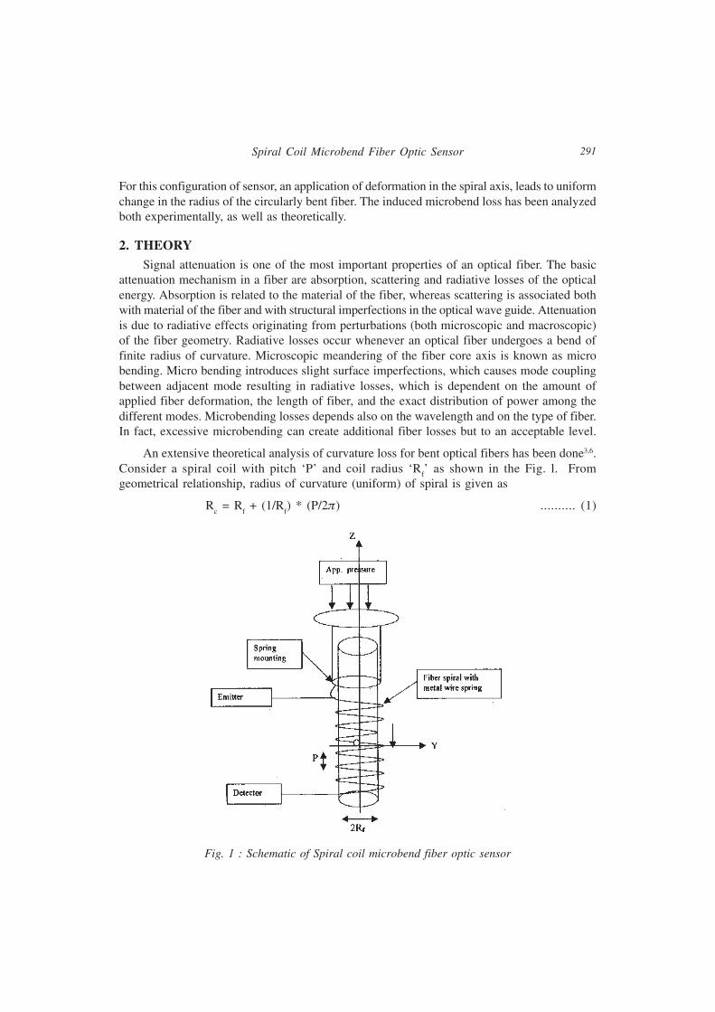
The Centronics parallel printer port pin configuration is shown in Figure 1. It effectivelyconsist of twelve output lines and five input lines, From the view point of the software, theIBM PC printer port consist of three hardware ports located at three successive addresses.The first port controls the eight data lines, the second port for reading the status (by the PC)of the printer and the third port to send control signals (from PC) to the printer. By just alteringthe on-board hardware of the PC, one can convert the data and control ports of the printer asinput ports. The acknowledge input line (pin 10 of D connector) can be used to trigger
P. Thimmaiah, K.R. Rao and E.R. Gopal
241
Fig.1 The Centronics parallel printer port configuration.
Fig.2 The pin designations of status and control ports.
hardware interrupt in the computer. This is possible by the IRQ of the control port. The pindesignations of the status and control ports are shown in Figure 2. The status port is readonly. As mentioned earlier the data and control ports can be configured as read/write ports5.
External Device Control using IBM PC’s Centronics Printer Port
242
2.2 Hardware description of the stepper motor interfaceThe stepper motor used in the present study is the one which was collected from
junk of a dismantled, obselete 5 ¼” floppy drive mechanism. This is a tiny stepper motorand gives a stepping angle of 1.8O in each step. Further, mounting and handling of themotor are easy. The average maximum current drawn by the motor is approximately200 mA.
A suitable power amplifier is designed for configuring the transistor pair (SL100, TIP122)in Darlington configuration, To isolate the PC hardware from the interface hardware, optoisolators (MCT2E) are used.
The stepping motor is clamped to a board as shown in Figure 3. As depicted inFigure 4, the four signal lines to drive the power amplifier via the LEDs of opto isolators areobtained from the four LSBs of the data port of the Centronics parallel printer port of the PC.
3. SOFTWARE OPERATIONThe software to drive the stepper motor is written in assembly language using macro
assembler MASM 86. A BIN file is created using EXE2BIN command. This file occupiesvery less memory space on the hard disk. Thus, whenever the file name: STEPPER is typedon the command line, the program is executed by the PC. The program is written in such away that it gets terminated at a pressing of any ASCII key on the key board. The programtermination keeps the motor in power down mode.
In conventional DIOT cards, 8255s are used to accomplish the parallel interfacing. Thisscheme needs 8255 to be initialized first, before using the ports. In the present work, the useof Centronics parallel port doesn’t need any initialization.
Fig.3. Photograph of the stepper motor clamped to a board
P. Thimmaiah, K.R. Rao and E.R. Gopal
243
The flow chart for rotating the motor at a stepping angle of 1.8O continuously is shownin Fig. 5. During this process of rotation, if the user presses any of the ASCII key, the programgets terminated by keeping the motor in the power down mode.
The software listing of the program is depicted at the end of the paper.
4. SAMPLE APPLICATIONA linear voltage variation for single-slope/dual-slope analog-to-digital conversion technique
is needed. In the present study, such a linear voltage variation with time is obtained by thecombination of stepper motor with a multi-turn potentiometer. The linear variation of voltage(Fig. 6) is realised by linear variation of potentiometer with the stepper motor whose rotationis controlled via the Centronics printer interface port.
Fig.4. The interface circuit developed in the present work.
External Device Control using IBM PC’s Centronics Printer Port
244
Fig.5. Flow chart for rotating the stepper motor at a stepping angle of 1.8O.
Fig.6. Photograph of the Oscilloscope trace obtained during the linear voltage variationobtained by stepper motor rotation.
P. Thimmaiah, K.R. Rao and E.R. Gopal
245
5. PERFORMANCEThe software and hardware developed in the present study were tested on both 50 MHz
80386 machine and Pentium III machine working at 1 GHz. It is found that the Centronicsprinter port addresses were different in these machines.
6. CONCLUSIONThe scheme of interfacing the outside world devices with PC via Centronics printer port
provides a convenient and versatile method of realizing input/output port. The case study ofinterfacing stepping motor with PC via Centronics port opens gates for control applications.Further, it is a good hardware and software exercise for a student when implemented as anexperiment in the laboratory.
of Liquids”, J. Instrum. Soc. India, 31, 256-261 (2001).
2. G.S. Babu, K.R. Rao and E.R. Gopal, “A PC-Based Amplitude Ratio Measurement”, Acta CienciaIndica, 27, 4, 291-295 (2001).
3. PC Hardware; Complete Reference, Zacker and Rourke, Tata McGraw Hill, 2000.
4. Assembly Language Programming and Architecture of the IBM PC, Yu and Marut, TataMcGraw Hill, 2000.
5. The Pentium Microprocessor, Antonakos, Pearson Edition, 2001.
External Device Control using IBM PC’s Centronics Printer Port
246 P. Thimmaiah, K.R. Rao and E.R. Gopal
247External Device Control using IBM PC’s Centronics Printer Port
248
EVALUATION OF FUZZY LOGIC CONTROLLER FORRESISTANCE SPOT WELDING PROCESS
Madhubala T. Kadavarayar, K Asok Kumar* and S. Arumugam**Department of Physics, Regional Engineering College, Tiruchirappalli 620 015.
*WRI, Bharat Heavy Electricals Ltd., Tiruchirappalli 620 014.**Department of Physics, Bharathidasan University, Tiruchirappalli 620 024.
ABSTRACT
The fuzzy logic based resistance spot welding controller with primary side feedback isevaluated in the present work. The controller is evaluated under three influencing factorsnamely, fit up, secondary impedance, and surface condition (rusted). Spot welding trialsare conducted on 1 mm + 1mm low carbon steel sheets. Tensile shear loads and nuggetdiameters are measured in addition to recording of current and voltage waveforms as afunction of time. Dynamic resistance and firing delay are derived from the waveforms ofcurrent and voltage. The present study reveals that the controller performance issatisfactory in maintaining the consistency of weld quality against the three factorsstudied.
1. INTRODUCTIONResistance spot welding is a very popular welding method and is used extensively in mass
production of consumer goods, automobiles and sheet metal products. With adaptation of ISO9000 and TQM, it is essential to have process control at every stage of product manufacturingin industries to ensure the quality of products making use of resistance welding as a fabricationprocess. In this regard, extensive use of sophisticated resistance spot welding controllers withfeedback capabilities is essential. Although a number of controllers are available in the market[1,2], there is less awareness among resistance welding users in India about relative merits ofdifferent types of feedback controllers. The present work aims at bringing out a possibleapproach for evaluation of resistance welding controllers and assessing the performance ofthe fuzzy logic based dynamic resistance controller.
2. EXPERIMENTALIn the present work, for the evaluation of the controller, cold rolled sheet of low carbon
steel of 1 mm to 1 mm is used. For spot welding trials, a rocker arm type spot welding machineof 30 KVA capacity is used with a primary feedback type fuzzy logic based dynamic resistancecontroller [3]. The electrode tip diameter of 6 mm is selected.
J. Instrum. Soc. India 32 (4) 248 - 260
249
The effect of the three critical factors, namely fit up, secondary impedance, and surfacecondition, are studied in order to test the performance of the controller. Fit up is consideredas one of the factors as it is very difficult to maintain the exact fit up between the sheets[4] in such industries as the automobile and sheet metal industries. In the present work, asheet of 1mm is sandwiched between two sheets of 1mm to 1mm to artificially create poorfit up condition. The effect of impedance is considered as another influencing factor,since in many applications, resistance welding is used in the processing of large sizematerial. In such cases, introduction of large size material in the secondary of thetransformer in the spot welding machine will introduce variation in current at differentpositions. Hence, in this study a plate of mild steel (size: 100*150*10mm) is introduceddeliberately to increase the impedance in the secondary side. In order to study the influenceof surface cleanliness on the quality of the welds, trials are under taken with rusted carbonsteel sheets.
A computer based data acquisition system (HBM make) is used to record current andvoltage as a function of time while welding. Toroid coil is used for measurement ofcurrent and a pick up coil in the electrode tips is used to measure the voltage [5]. Thepurpose of recording current and voltage is to assess the exact firing angle anddynamic resistance for every cycle [6-8] so that the controller feedback performance canbe analyzed.
The firing delay is an important parameter in determining the performance of thecontroller. The firing delay is the distance between the crossover point and the starting ofthe next half cycle. This can be measured from the voltage waveform. Both the firing delayand dynamic resistance for each cycle is computed and plotted as a function of time foreach welding condition. For testing of spot weld integrity, the transverse tensile shear testis performed in a universal testing machine. After tensile shear testing, nugget diameter ismeasured for all the joints. Nugget diameters are measured at two positions perpendicularto each other and the average value is recorded.
3. RESULTS AND DISCUSSION
For evaluation of fuzzy logic type dynamic resistance controller [3], current and voltageas a function of time are recorded while spot welding. The trials are conducted with fuzzycontrol ON/OFF condition for each of the influencing parameters namely fit up, surfacecondition, and the secondary impedance. Ten trials are conducted in each setting with theestablished welding conditions (8kA rms current, 8 cycles, load 100 kgf). Two weld cyclesare used. The first weld cycles (2 cycles) are used for ensuring the consistency ofsurface condition. In the second weld cycles, the fuzzy logic based dynamic resistancecontrol is exercised. The average and standard deviation values of the test results for thesetrials are considered for evaluation. Table 1 summarizes the tensile shear load and nuggetdiameter results.
Evaluation of Fuzzy Logic Controller for Resistance Spot Welding Process
Table 1 : Tensile shear loads and nugget diameters for various conditions
Condition
Fig. 1. : Current - Poor Fit up Condition
Madhubala T. Kadavarayar, K Asok Kumar and S. Arumugam
251
3.1 Influence of poor fit upBehavior of current and voltage : Figures 1 and 2 show the graphical recordings of
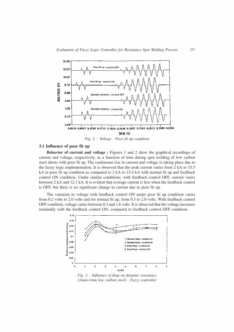
current and voltage, respectively, as a function of time during spot welding of low carbonsteel sheets with poor fit up. The continuous rise in current and voltage is taking place due tothe fuzzy logic implementation. It is observed that the peak current varies from 2 kA to 15.5kA in poor fit up condition as compared to 2 kA to 15.4 kA with normal fit up and feedbackcontrol ON condition. Under similar conditions, with feedback control OFF, current variesbetween 2 kA and 12.1 kA. It is evident that average current is less when the feedback controlis OFF, but there is no significant change in current due to poor fit up.
The variation in voltage with feedback control ON under poor fit up condition variesfrom 0.2 volts to 2.0 volts and for normal fit up, from 0.3 to 2.0 volts. With feedback controlOFF condition, voltage varies between 0.3 and 1.8 volts. It is observed that the voltage increasesnominally with the feedback control ON, compared to feedback control OFF condition.
Fig. 2. : Voltage - Poor fit up condition
Fig. 3. : Influence of fitup on dynamic resistance(1mm+1mm low carbon steel) - Fuzzy controller
Evaluation of Fuzzy Logic Controller for Resistance Spot Welding Process
252
Behavior of dynamic resistance: Figure 3 shows the graphical recordings of dynamicresistance (during second weld stage alone) as a function of time in different conditions i.e.,normal or poor fit up with feedback control ON or OFF. From the curves, it is observed thatthe dynamic resistance reaches peak value in the second cycle irrespective of controllerfeedback condition.
In case of poor fit up with feedback control ON, initially dynamic resistance changesfrom 87 to 137 micro ohms i.e. an increase by 63%. Followed by that it drops to 120 microohms (13% drop). Subsequently there is an overall increase in dynamic resistance of 8 microohms in the remaining cycles i.e. around 6.6% increase.
In case of normal fit up, initially, the increase in the dynamic resistance is about 30%from the initial value of 114 micro ohms at first cycle. In the fourth cycle, it drops to a minimumof 114 micro ohms (30%). Subsequently, the overall increase in dynamic resistance in theremaining cycles is 16.6%. The percentage of increase of resistance is more in the first twocycles with poor fit up condition as compared to normal fit up due to the poor formation ofcontact at the interface.
Fig. 4. : Influence of poor fit up on firing delay(1mm+1mm low carbon steel) - Fuzzy controller
Behavior of firing delay: Figure 4 shows the graphical recordings of firing delay fordifferent conditions. Under feedback control ON and OFF condition in both normal fit up andpoor fit up condition, the firing delay was ranging between 0.42 and 4.58 milliseconds. Underfeedback control ON condition with poor fit up and feedback control OFF with normal fitup, variation in firing delay ranges from 2.5 to 4.58 milliseconds. The major variation in firingangles were noticed only in the last four cycles. With feedback control ON and poor fit up,the increase in firing angle shows that there is a decrease in current with poor fit up due tocorrective action of the controller. The current recordings again support this observation.Further, similar behavior was reported for learning curve type constant current controller byJerry E. Gould[3] under different fit up conditions.
Madhubala T. Kadavarayar, K Asok Kumar and S. Arumugam
253
Tensile shear test and nugget diameter measurement results: Table 1 shows the tensileshear test and nugget diameter measurement results. It is found that with poor fit up of 1mm,the tensile shear load marginally increases from 606 kgf to 622 kgf with feedback controlON condition. The standard deviation of tensile shear load value in poor fit up condition is82.2 as against the normal condition value of 13.4. but, the nugget diameter decreases form5.3 mm in normal fit up condition to 4.6 mm in poor fit up condition. The standard deviationof nugget diameter in the case of poor fit up condition is 1.13 mm as against the normalcondition value of 0.32 mm. This means that there is reduction both in tensile shear load valueand nugget diameter due to poor fit up. But, the scatter or standard deviation value for boththe measured values is marginally increasing under poor fit up condition and when the constantcurrent feedback control is OFF.
Fig. 5. : Current - Secondary Impedance
3.2 Influence of Secondary ImpedanceBehavior of current and voltage : Figure 5 and 6 show the graphical recordings of
current and voltage, as a function of time during spot welding of low carbon steel sheetswith high secondary impedance. The continuous rise in current and voltage is taking placedue to the fuzzy logic implementation. It is observed that the peak current varies from 2.2 kAto 15.6 kA whereas the variation with no impedance and feedback control ON is 2.3 to 15.5kA. There is no significant change in the current waveforms for both the conditions.
The variations in voltage ranges from 0.2 volts to 2.0 volts in high impedance conditionwith feedback control ON. The same in the case of no impedance and control ON is 0.3 to2.0 volts. It is observed that there is no significant change in voltage in either case.
Evaluation of Fuzzy Logic Controller for Resistance Spot Welding Process
254
Fig. 7. : Influence of secondary impedance on dynamic resistance(1mm+1mm low carbon steel) - Fuzzy controller
Behavior of dynamic resistance : Figure 7 shows the graphical recordings of dynamicresistance as a function of time in different conditions i.e., no impedance with feedback controlON and OFF and high secondary impedance with control ON and OFF. From the curves, itis observed that dynamic resistance reaches peak value in the second cycle irrespective offeedback control condition. In case of high secondary impedance with control ON, dynamicresistance changes from 93 to 134 micro ohms i.e., an increase by 43%. Followed by that,
Fig. 6. : Voltage - Secondary Impedance
Madhubala T. Kadavarayar, K Asok Kumar and S. Arumugam
255
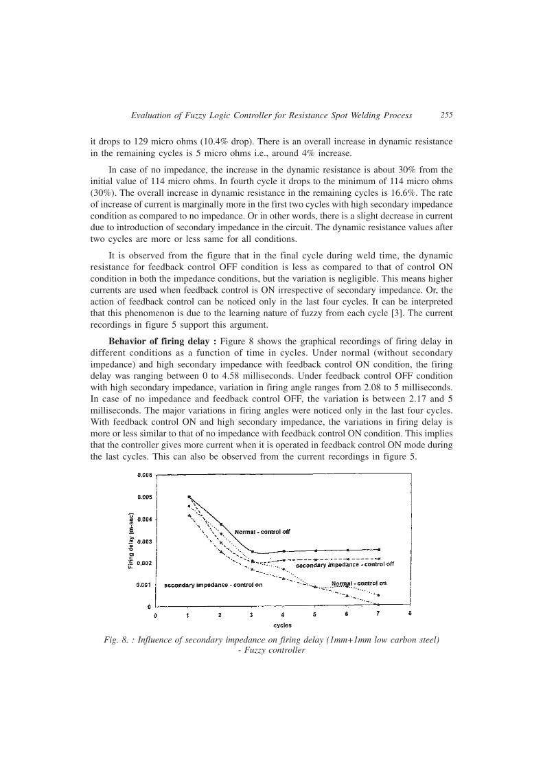
it drops to 129 micro ohms (10.4% drop). There is an overall increase in dynamic resistancein the remaining cycles is 5 micro ohms i.e., around 4% increase.
In case of no impedance, the increase in the dynamic resistance is about 30% from theinitial value of 114 micro ohms. In fourth cycle it drops to the minimum of 114 micro ohms(30%). The overall increase in dynamic resistance in the remaining cycles is 16.6%. The rateof increase of current is marginally more in the first two cycles with high secondary impedancecondition as compared to no impedance. Or in other words, there is a slight decrease in currentdue to introduction of secondary impedance in the circuit. The dynamic resistance values aftertwo cycles are more or less same for all conditions.
It is observed from the figure that in the final cycle during weld time, the dynamicresistance for feedback control OFF condition is less as compared to that of control ONcondition in both the impedance conditions, but the variation is negligible. This means highercurrents are used when feedback control is ON irrespective of secondary impedance. Or, theaction of feedback control can be noticed only in the last four cycles. It can be interpretedthat this phenomenon is due to the learning nature of fuzzy from each cycle [3]. The currentrecordings in figure 5 support this argument.
Behavior of firing delay : Figure 8 shows the graphical recordings of firing delay indifferent conditions as a function of time in cycles. Under normal (without secondaryimpedance) and high secondary impedance with feedback control ON condition, the firingdelay was ranging between 0 to 4.58 milliseconds. Under feedback control OFF conditionwith high secondary impedance, variation in firing angle ranges from 2.08 to 5 milliseconds.In case of no impedance and feedback control OFF, the variation is between 2.17 and 5milliseconds. The major variations in firing angles were noticed only in the last four cycles.With feedback control ON and high secondary impedance, the variations in firing delay ismore or less similar to that of no impedance with feedback control ON condition. This impliesthat the controller gives more current when it is operated in feedback control ON mode duringthe last cycles. This can also be observed from the current recordings in figure 5.
Fig. 8. : Influence of secondary impedance on firing delay (1mm+1mm low carbon steel)- Fuzzy controller
Evaluation of Fuzzy Logic Controller for Resistance Spot Welding Process
256
Tensile shear test and nugget diameter measurement results: Table 1 shows thetensile shear test results and nugget diameter results. It is found that with high secondaryimpedance, the tensile shear load marginally decreases from 606 kgf to 605 kgf with feedbackcontrol ON condition. The standard deviation with secondary impedance condition is 22.1 asagainst the normal condition value of 13.4. But, the nugget diameter decreases from 5.3 mmin normal condition to 4.6 mm at high impedance condition. The standard deviation in thecase of high impedance condition is 0.28 mm as against the normal condition value of 0.32mm. There is only marginal variation of tensile shear load and nugget diameter.
3.3 Influence of Surface ConditionBehavior of current and voltage: Figures 9 and 10 show the graphical recordings of
current and voltage, respectively, as a function of time during spot welding of low carbon
Fig. 9. : Current - Poor Surface Condition
Fig. 10. : Voltage - Poor Surface Condition
Madhubala T. Kadavarayar, K Asok Kumar and S. Arumugam
257
steel plates with rusted surfaces. The continuous rise in current and voltage is taking placedue to the fuzzy logic implementation. In the case of rusted surfaces and feedback controlON, it is observed that the peak current varies from 2.3 kA to 16.1 kA. The variations involtage ranges from 0.4 volts to 2.66 volts. With normal surface and feedback control ONcondition, the variation in current is between 2.3 to 15.4 kA and voltage varies between 0.3to 2 volts. With feedback control OFF and rusted surfaces, these values are between 2.0 to12.6 kA and 0.3 to 1.8 volts. It is noticed that the increase in current is more gradual in caseof rusted surfaces as compared to the normal condition. This may be due to the initial highresistance exhibited by the oxide layer on the surface.
Behavior of dynamic resistance: Figure 11 shows the graphical recordings of dynamicresistance as a function of time with the conditions of normal cleaned plates with feedbackcontrol ON and OFF, rusted sheets with feedback control ON and OFF. From the curves, itis observed that dynamic resistance reaches peak value in the second cycle irrespective offeedback control ON or OFF except in rusted sheet and control ON condition. In the case ofpoor surface conditions with feedback control ON, dynamic resistance changes from 116 to191 micro ohms i.e., an increase by 64.6%. Followed by that, it drops to 160 micro ohms(16.2% drop). There is an overall change in dynamic resistance in the remaining cycles of 5micro ohms i.e., around 3% increase. In case of normal surfaces, the increase in the dynamicresistance is 30% from 114 micro ohms. In the fourth cycle, it drops to the minimum of 114micro ohms (30%). The overall increase in dynamic resistance in the remaining cycles is16.6%.
It is evident from the figure that the dynamic resistance values are higher for rusted sheetsin the first 5 cycles. This is due to higher contact resistance offered by the rusted surfacesin the first few cycles. When the feedback control is ON, there is variation in dynamicresistance between the rusted surfaces and the normal surfaces only in the first five cycles.There is reduction in current in the case of rusted sheets in the first cycle as observed in thecurrent waveform. In the last 4 cycles, as the bulk heating takes place, the dynamic resistanceof the rusted plates well be same as that of the normal plates. When rusted surfaces are present,there is significant increase in the dynamic resistance overall.
Fig. 11. : Influence of surface condition on dynamic resistance (1mm+1mm low
Evaluation of Fuzzy Logic Controller for Resistance Spot Welding Process
258
Behavior of firing delay : Figure 12 shows the graphical recordings of firing delay indifferent conditions as a function of time in cycles. With feedback control ON, normal/rustedsurface condition, the firing delay was ranging between 4.2 to 4.58 milliseconds. Underfeedback control OFF condition with rusted surfaces, variation in firing angles ranges from1.67 to 4.58 milliseconds. With normal surface and feedback control OFF, the variation infiring delay is between 2.5 and 5 milliseconds. The major variations in firing angles were noticedonly in the last four cycles. This implies that controller gives more current when it is operatedin feedback control ON mode in the last four cycles. This can be attributed to the high contactresistance in the initial cycles.
Fig. 12. : Influence of surface condition on dynamic resistance(1mm+1mm low carbon steel) - Fuzzy controller
Tensile shear test and nugget diameter measurement results: Table 1 shows thetensile shear test results and nugget diameter results. It is found that with rusted surfaces,the tensile shear load marginally increases from 606 kgf to 630 kgf with control on condition.The standard deviation of tensile shear load in rusted surface condition is 30.55 as against thenormal condition value of 13.4. But, the nugget diameter decreases from 5.3 mm in normalcondition to 4.8 mm at rusted surface condition. The standard deviation of nugget diameterin the case of rusted surface condition is 0.71 mm as against the normal condition value of0.32 mm. There is only marginal variation of tensile shear load value and nugget diameter.But, the scatter or standard deviation value for both the measured values is increasing underpoor surface condition and when the constant current feedback control is OFF.
4. DISCUSSIONThe results of tensile shear test and nugget diameter measurement can be plotted in a
single graph to study the relative significance of the three factors namely fit up, surfacecondition, and secondary impedance as proposed by H. Polrolniczak [9]. Figure 13 showsthe typical curve of significance of different influencing parameters with tensile shear load asresponse. In this case, the tensile shear load is expressed as ratio of actual shear load andexpected load as per DVS specification for lmm + 1mm (640 kgf). Likewise, a graphrepresenting nugget diameter ratio as response in Y-axis and the typical plot are shown in
Madhubala T. Kadavarayar, K Asok Kumar and S. Arumugam
259
figure 14. It is found from the tensile shear load ratio that only in the case of feedback controlOFF condition the weld strength has been reduced. This indicates that the controller is ableto perform well against all three influencing variables. On the contrary, nugget diameter ratiorevealed that all the factors including the controller mode reduce the nugget diameter fromthat of normal condition weld. But the reduction in ON mode is less than 10% and provedthat adaptation of control maintains the nugget diameter more than 90% against poor fit up,secondary impedance and rusted surface condition. The steepness of curves 3 and 5 in figure14 (feedback control OFF with poor fit up and secondary impedance) shows that there issignificant effect on nugget diameter compared to poor surface condition.
Fig. 14. : Nugget diameter results for fuzzy controller
Fig. 13. : Tensile shear test results for fuzzy controller
5. CONCLUSIONSBased on the present studies, with resistance spot welding of 1mm + 1mm low carbon
steel, the following conclusions can be drawn.
1. Fuzzy logic dynamic resistance based spot welding controller is able to ensure theconsistency of tensile shear load and the nugget diameter against the fit up, secondaryimpedance, and surface condition.
Evaluation of Fuzzy Logic Controller for Resistance Spot Welding Process
260
2. The response of the controller for the variation of fit up, secondary impedance andsurface condition is different.
3. Process waveform analysis revealed that the fit up, high secondary impedance, andsurface condition affected the process stability only in the initial few cycles of welding timebut subsequently there is no significant effect on spot weld quality due to the compensationby the controller.
REFERENCES1. “Correlation of process recordings with weld quality and evaluation of the controllers”,
K. Asok Kumar, Dr. W. Faber, N. Winkler, Workshop on Trends in resistance welding in Indianindustries, Welding Research Institute and Indian Institute of Welding, Tiruchirappalli, India,November 1995.
2. “Feedback controller to achieve 100% weld quality- state of art”, S. Manoharan, V.R. Samuel,K. Asok Kumar, Dr. K.G.K. Murti, Workshop on Trends in resistance welding in Indianindustries, Welding Research Institute and Indian Institute of Welding, Tiruchirappalli, India,November 1995.
3. “Method of controlling resistance welding using Fuzzy reasoning”, Miyachi TechnosCorporation, European patent office, publication number 0 669 182 2A.
4. “Effect of fit up conditions when using constant current control systems for resistance spotwelding”, Jerry E. Gould, Menachem Kimchi, Tom Mitchell, International Congress andExposition, Detroit, Michigan, U.S.A., 1993.
5. “Evaluation of dynamic resistance as quality criterion for resistance spot welding”, K. AsokKumar, S. Manoharan, V.R. Samuel, Dr. K.G.K. Murti, Welding in automobile industry, nationalseminar, IIW, Jamshedpur, April 1996.
6. “Monitoring dynamic resistance during the formation of resistance spot welding”, Peter Kuy,Welding Journal, 1974.
7. “Significance of dynamic resistance curves in the theory and practice of resistance spotwelding”, S. Bhattacharya and D. Andrews, Welding and Metal Fabrication, September 1974.
8. “Characterization spot welding behavior by dynamic electrical parameter monitoring”, D.W.Dickinson, et al, Welding Journal, June 1980, p. 170 S.
9. “Equipment for quality control of resistance spot welding – A comparison of their capabilitiesand their selection criteria”, H. Polrolniczak, Proceedings of resistance welding conference,Duisburg, Germany, 1989, p. 80.
Madhubala T. Kadavarayar, K Asok Kumar and S. Arumugam
261
MODELING OF PIEZO - ELECTRIC FILMTHICKNESS MONITOR USING PSPICE
A. K. Walunj* and A. D. Shaligram***Department of Electronic Science, Poona College Camp, Pune- 411001.
**Department of Electronic Science, Pune University, Pune- 411007.
ABSTRACT
Thin films are deposited on various substrates using vaccum evaporation deposition orsputtering techniques. Online Thickness Monitors are generally used in such systems.This paper is an attempt to model thickness monitor using PSpice. Equivalent circuitmodel of the piezo-electric crystal is chosen and a crystal oscillator circuit performanceis analyzed. We thickness of the deposited film alters the L and C parameters. This changeis included in the simulation files using different values corresponding to different filmthickness. The Tran analysis request probes the piezo-electric circuit performance. PSpiceis used as a very powerful and accurate simulation tool to monitor the film thickness.The results of simulations presented for different material thickness of a crystal are ingood agreement with experiments.
1. INTRODUCTIONThe best technique for a specific application or process depends upon the film type, the
thickness of the thin, the accuracy desired, and the use of the film. These criteria includesuch properties as film thickness, film transparency, film hardness, thickness uniformity,substrate smoothness, substrate optical properties and substrate size. In many cases there isno single best technique and the particular one chosen will be determined by the personalpreferences of the investigator.
There are various mechanical, electrical and magnetic methods for measuring filmthickness. Most of these methods will not be considered in detail because of their inherentlimitations and narrow applications. However the electrical properties which lend themselvesfor film thickness measurement are dielectric strength (breakdown voltage), capacitance andresistance of the film. Because of the unreliability of electrical breakdown voltage as an inductorof film thickness this technique is not recommended. Capacitance measurements aresometimes used for determining the thickness of dielectric films deposited on conductingsubstrates. The capacitance is inversely proportional to the film thickness, directly proportionalto the area of the which is deposited on the dielectric film (provided the area is large enoughto keep edge effects to a minimum) and directly proportional to the dielectric constant of thefilm. Problematical requirements for this measurement are that there must be no pinholes in
J. Instrum. Soc. India 32 (4) 261- 268
262
the film and that the dielectric constant must be accurately known. Usually the dielectricconstant of the film is strongly dependent on the deposition conditions.
Since there are other more accurate thickness- measuring techniques for dielectric films,capacitance measurements are useful for determining the dielectric constant of thin films[1].Thin film ferroelectrics are used at microwaves. If the thickness of the film is comparablewith the correlation radius the size effect appears in the film, i,e. dielectric permitivity of filmdepends on its thickness[2].
The frequency of vibration of the crystal is the crystal is inversely proportional to itsthickness and there are mechanical limits to how thin crystal can be cut and polished. Crystalscan be manufactured to have fundamental frequencies from few kHz up to about 10 MHz.Higher frequencies can be obtained by operating the crystal in overtone mode, which producesmultiples of the fundamental [3]. Thus the properties, thickness monitors used for manufacturingof crystals or crystal based instruments requires special attention and care is utmost in thedesign and development of such products. Such crystals oscillators are the standard meansof maintaining the frequency of radio transmitting stations at the assigned values and alsofind extensive use in the reception of signal from transmitter stations of specified frequenciesfor example, in connection with aircraft-to-ground radio communications.
Piezo-electric materials
The most accurate and stable oscillators uses piezoelectric crystals in place of LC circuits.The piezoelectric effect is found in number of materials including quartz and certainmanufactured ceramics materials. Quartz is the material most commonly used for very stableoscillators. Piezoelectric properties are exhibited by a number of natural crystal substances ofwhich the most important are quartz, Rochelle salt, and tourmaline, The effect is exhibited tothe greatest degree by Rochelle salt, which is used in crystal microphones and loudspeakers.Quartz though exhibiting the piezoelectric effect to a smaller degree than Rochelle salt isemployed for low frequency control in oscillators because of its permanence, lowtemperature coefficient and high Q. Tourmaline is similar in these respects to quartz but ismore expensive [4]. The piezoelectric effect is an electromechanical process where theapplication of an alternating voltage creates a mechanical stress in the material, which causesthe material to vibrate. The crystal has a natural mechanical resonant frequency and thevibrations are greatest when the applied electrical signal corresponds to this mechanicalresonant frequency.
Film Thickness MonitorsIn conventional crystal monitors and controllers for thin film technology, the quartz crystal
in the sensor in the sensor head determines the frequency of operation of the RF power supply.That is the power supply must oscillate at the crystal fundamental resonant frequency duringnormal operation the crystal’s mass increases (due to deposition) and its mechanical propertieschange. The coupling between the crystal and the RF drive electronics at the fundamentalfrequency weakens and eventually crashes when the crystal hops to a higher harmonicfrequency. The measurement circuit based on the history changes in the fundamental frequencyis unable to resolve the information and measurement’ fails’ [5].
A. K. Walunj and A. D. Shaligram
263
Epitaxy is a deposition process that has a thin film of single crystal material applied to asilicon wafer. Usually, but not always, it is the thin layer of crystal is the same compositionas the crystal wafer. One example of where epitaxy is used is during the fabrication of lightemitting diodes. Carefully made materials and doping process are used in conjunction withhigh temperature diffusions with the help of epitaxy techniques to generate the light. Epitaxyis also make the collector and base regions for transistors [6].
Computer aided simulation is a powerful aid and during the design or analysis of electroniccircuits, instruments and semiconductor devices. The conventional film thickness monitorsand techniques require to set start and stop time, substrate on which deposition of film wouldbe deposited using suitable processes. It involves large amount of processing time and materialcost for the production of variety of thickness of semiconductor devices leads to constructthe desired circuit or instrument. As these techniques are useful but found to complex, lowprecision and time consuming thus need to develop and use of Faster technique to controlthese limitations.
PSpice i.e. PC version of Simulation Program with Integrated Circuit Emphasis has becomea common tool for analogue and digital simulations and widely used, even for mixed modecircuit design or process and analysis. It allows the designer to construct entirely new circuitmodel i.e. crystal without fabricating the actual circuit or without deposition of actual film onthe desired substrate under the control or film thickness monitoring or supervision. The circuitperformance and reliability or any failure can be tested by replacing the equivalent electricalcircuit or model and analyzed for different variable parameters and hence monitoring theprocess. This technique is more precise, faster, and cost effective.
The most widely known and used circuit simulation program is PSpice, originally developedby Laurence Negal, in 1975 at the university of California at Berkeley. It is a general purposecircuit simulator that simulates circuits and performs variety of analysis. It also allows userto use available models and external models. Computer circuit simulation is now consideredas an essential step in the design of semiconductor devices, circuits etc. because withoutsimulation the number of “trial runs” necessary to produce a working circuit would greatlyincrease cost of circuit[7].
2. (A) CRYSTAL MODEL
A crystal consists of a thin plate of quartz, a few millimeters in diameters withelectrodes on opposite faces. Wires are attached to the metal electrodes and it is sealed into ametal case. As far as the electrical equivalent circuits associated with a vibrating quartzcrystals are concerned the crystal can be replaced by the resonant circuit LCC1R of Fig. l.Here C1 represents the electrostatic capacitance between the crystal electrodes when the crystalis not vibrating and the series combination of L, C and R represents the electricalequivalent of the vibrational characteristics of the material. The inductance L is the electricalequivalent of the crystal mass that is effective in the vibration, C is the electrical equivalentof the mechanical compliance, while R represents the electrical equivalent of themechanical friction.
Modeling of Piezo - Electric Film thickness monitor using PSpice
264
(B) Model Parameters :
The magnitudes of L, C, R and C1 that enter into the equivalent electrical network of thevibrating quartz crystal depend upon the way in which the crystal is cut, its size and the typeof vibrations involved. Numerical values can be calculated when these factors are known andhave of which those listed in Table 1. are for a typical quartz crystal [8].
Resonant frequency Q = 23,000 (approx.)(thickness vibration)
Series resonance.........427.4 kc
Parallel resonance........430.1 kc
Table 1 : Characteristics of a Typical Quartz Crystal
3. EXPERIMENTAL SETUPElectrical circuits involving piezoelectric crystals can be therefore analyzed by replacing
the crystal with its model i.e. equivalent electrical network and then determining the behaviorof the resulting circuits or an instruments. Which would help to predict the oscillator utmostresponse, accuracy and stability corresponding to crystal thickness and change in the itscharacteristics can easily be monitored. PSpice is used as tool to monitor and probe the crystaloscillator frequency response with time. The Tran command does the essential transient analysisof a crystal oscillator circuit, The Probe analysis request displays the various fundamentalfrequencies pertaining to different film thickness and crystal parameters used in before actuallythey are designed and produced by the manufacturer or for the design and development ofnew instrument.
The number of circuits were created and every time the circuit file was created by usingPSpice format. It also facilitates to write different circuit files with different circuit data andparameters under the single file name and allows to simulate the circuit results in few seconds.
A. K. Walunj and A. D. Shaligram
265
To meet with the desired frequency performance andspecifications of a suitable crystal oscillator circuit for knownparameters it is often required to pass through number ofiterations. A quartz crystal can be used to control thefrequency of oscillator by so locating the crystal in theoscillator circuit that the equivalent network of the crystali.e. crystal model as depicted in Fig. 1(a) and fig. (2)respectively.
It becomes the part of the resonant circuit that wouldnormally control the frequency. Typical crystal oscillatorcircuit is a generic circuit that uses two MOSFET’s namelyM1 (NMOS), M2 (PMOS) and a X-Tal in such manner thatit forms a series LCR network placed in between input andoutput n 1 and 4 along with a VDD =+5V DC regulatedpower supply as illustrated in Fig. 2.
Fig. 2. Crystal OssillatorCircuit
4. RESULTS AND CONCLUSIONSThe sensor crystal oscillator circuit designed to be used with industry standard MHz sensor
crystals. The oscillator’s characteristics enable it to obtain the exact film deposition on itssurface and the change in dimensions and leads to change its electrical equivalent parametersinductance, capacitance and resistance (less net effect) as shown in table 1 and 2 respectively.
● Total shunt or mounting Capacitance ……………………………..(C1) = 5.8 Pf.
● Elasticity i.e. Crystal equivalent Capacitance………………………(C) = 0.042 Pf.
● Mech.. Friction i.e. Resistance…………………………………….. (R ) = 50 W
Pspice probes the transient waveforms of the crystal oscillators and provides theperformance readily for different materials of varying thicknesses as illustrated in the Fig. 3
Table 2 : Crystal frequency as function of Mass i.e. inductance
Modeling of Piezo - Electric Film thickness monitor using PSpice
266
Table 3 : Crystal frequency as function of Film thickness or Capacitance
● Total shunt or mounting Capacitance …………………………….(C1) = 5.8 Pf.● Mass of the quartz crystal is analogous to inductance…………….(L) = 3.3 Henry.● Mech.. Friction i.e. Resistance………………………………….... (R ) = 50 W
Fig. 3. Transient analysis of a typical Piezo-electric Crystal oscillator circuit
Film Thickness Calculation : Early investigators noted that if one assumed that the additionof material to the crystal surface produced the same effect as the addition of an equal massof quartz. The following equation could be used to relate the film thickness to the change incrystal frequency
TK = N Pq (fq –f) / Pf f2
……………………(1)
A. K. Walunj and A. D. Shaligram
267
Where N=1.668 x 10 cm/sec Frequency constant for an AT cut quartz crystal vibratingin the thickness shear mode.
Pq = density of quartz (gm/cubic cm)=2.65 gm/ccf = Resonant frequency of the uncoated crystal.Fq = Resonant frequency of the loaded crystalTK = Film thicknessPq = Density of the film (gm/cubic cm)
This equation is proved to be adequate in most cases. However the constant ofproportionality is not actually constant because the term contains the crystal frequency whichof course changes. Because the achievable frequency change was small the change in scalefactor fell within acceptable limits.
In the late 1960’s improvements in sensor crystals and oscillator circuits resulted in asignificant increases in achievable frequency shift. At the same time, low cost integrated digitalcircuit became available allowing a significant increase in basic instrument accuracy so thatthe frequency squared term in the scale factor became important.
Substituting 1/period for frequency results in the following equation:
TK NqP (t tq)/ Pf ................... (II)
Where t = period of the loaded crystal (sec)
and tq = period of the unloaded crystal (sec)
Note that the constant of proportionality in this equation is constant.
The original assumption that the addition of a foreign material to the surface of the crystalproduced the same effect as that of the addition of an equal mass of quartz was, of coursequestionable. Crystals heavily loaded with certain materials showed significant and predictabledeviation between the film thickness measured and that predicted by equation II. Analysis ofthe loaded crystals as a one dimensional composite resonator of quartz and deposited film ledto the equation below.
Where : R = the acoustic impedance ratio which is obtained by dividing the acousticimpedance of quartz by the acoustic impedance of the deposited film.
This equation introduces another term into the relationship: the ratio of the acousticimpedance of quartz to the acoustic impedance of the deposited film. The acoustic impedanceis that associated with the transmission of a sheer wave in the material. Note that if the acousticimpedance ratio is equal to one, quartz, equation III reduces to equation II,
● Although the above equation still involves a number of simplifying assumptions, its abilityto accurately predict the film thickness of most commonly deposited materials has beendemonstrated.
● The use of microprocessors allows an equation as complex as equation 3 to be solvedeconomically and implemented in the Monitor . The actual film mass on the crystal isthen determined by applying the acoustic impedance correction factor.
Modeling of Piezo - Electric Film thickness monitor using PSpice
268
● At the start of the deposit or at zero the initial equivalent quartz mass and the initialscorrected film mass is stored. For each subsequent measurement the new corrected totalfilm mass is calculated and the film mass deposited since the start of deposit is determinedby subtracting the initial film mass from the total film mass.
● The film thickness on the crystal is calculated by dividing the film mass by the film density.
● The film thickness on the substrates is then calculated by multiplying the film thicknesson the crystal by a tooling factor. If the acoustic impedance parameter is changedfollowing a deposition, both the total and the initial film masses are recalculated. Thisallows the effect of the changed parameter value to be immediately displayed[9].
Fig. 4 is the plot of frequency as a function of different crystal masses and the natureshows that the frequency is decrease with increase in film mass. The frequency is inverselyproportional to the change in film capacitance as shown in Fig. 5. Hence the simulated resultsIs found to be benh mark of success of thin Film designing and monitoring process. Whichsaves time, efforts and material cost in manufacturing of desired semiconductor devices andcircuit applications.
REFERENCES1. L.L Maissel and R. Glang, “Handbook of Thin Film Technology”, MacGraw Hill-Inc., 1970.
2. T. E, Price Analog, “Electronics an integrated PSpice approach, Printice Hall, Europe, 1997.
3. F. E. Temen, “Electronics and Radio Engineering”, MacGraw Hill International EEE series, IVEd.1986.
6. O.G. Vendik and S. P. Zahko, “Modeling of Size Effects On Dielectric Response
7. Martin o’ Hara, Modeling of board level DC-DC Convetoers in SFICE, Electronic Productdesign, July, 1998.
8. Digital Thickness Monitor Model : DTM -1Ql, Operation and Maintenance Manual, Hind highVacuum Co. Pvt. Ltd, Bangalore.
Fig.4. Frequency variation function ofcrystal mass
Fig.5. Frequency variation as a functionof crystal capacitance
A. K. Walunj and A. D. Shaligram
269
DEVELOPMENT OF AN INSTRUMENT FORSOIL MOISTURE MEASUREMENT
S.R. Chaudhari*, S.A. Deuskar* and A.D. ShaligramDepartment of Electronic Science, University of Pune, Pune – 411007.
*Modern College, Shivajinagar, Pune - 411005.
ABSTRACT
This paper describes an attempt to develop low cost instrument for the measurement ofsoil moisture. There is variety of methods to determine percentage soil moisture. In thepresent work thermister based soil moisture sensor is used. The sensor is based onthermal conductivity. The heat transferred from the sensor to the soil is a function ofmoisture content in it. The calibration is performed to estimate soil moisture as a functionof change of resistance using thermister, which is compared with conventional gravimetricmethod. The sensor is optimized for its characteristics. This instrument finds direct usein the applications like automatic irrigation systems, where numbers of sensors areinstalled in the field. The flexibility and presetting arrangement are provided in order toadjust the irrigation rate for finite yield of crops. Further, online data acquisition of soilmoisture measurements can be done.
1. INTRODUCTIONIn the present work, thermister based moisture sensor[1] is developed using the principle
of thermal conductivity. This soil moisture sensor is used to design an instrument for themeasurement of soil moisture. The sensor is dipped into the soil where the moisture is to beestimated. The principle of the working of this type of soil moisture sensor is heat transferredfrom it towards the soil in predetermined time. The heat is generated in the sensor using small
heater and it is measured in terms of change of resistance of thermister, which is embeddednearby it. The thermister is used in current to voltage circuit where the moisture level is directlycorrelated with output voltage. An astable multivibrator using IC 555 monitors the heatingperiod of the sensor and cooling time of it up to the initial temperature. The ON time of theAstable multivibrator is designed, to make heater ON and conduct the heat through sensorinto the soil, when heater is made OFF, i.e. output of astable multivibrator in OFF time thepulse is generated by using differentiator, which drives the sample and hold circuit. The sampleand hold circuit holds the value of the output voltage of current to voltage converter. Sincethe thermister is used in feedback path of the current to voltage converter, the heat-transferredrate in predetermined time is measured in terms of voltage. The transfer of heat into the soilis strongly dependent on soil moisture content. Hence the soil moisture level can be determined
J. Instrum. Soc. India 32 (4) 269 - 274
270
in terms of output voltage. Using Analog to digital converter circuit the voltage is displayedon seven- segment display. This voltage with proper difference amplifier directly indicates themoisture level of the soil. Also this voltage is compared with comparator circuit, with presetvalue as per required for irrigation schedule and the irrigation solenoid valve can be controlledproperly. For better irrigation to the field number of sensors are to be used across the field.
2. THEORETICAL BACKGROUNDThe thermal properties of the soil are strongly dependent on soil moisture content. Hence
to measure soil moisture, the temperature gradient calibrated at various soil moisture levelscan be used. Soil thermal conductivity measurements describe the soil properties, which governthe flow of heat through the soil. The thermal conductivity is
defined as the quantity of heat that flows through a unit area in a unit time under a unittemperature gradient[2]. In the present work, heat is generated using 6.2 Ohm wire woundresistor enclosed in an aluminum rod, where the temperature is measured by placing thermisternearby to the resistor. The rod, which is now soil moisture sensor, is to be placed inside thesoil 4-5 cm inside, then by passing the current through the heater for predetermined time theflow of the heat from the sensor towards the soil is measured.
As shown in fig (1) aluminum rod of length 7 cm and diameter of 2 cm is tapered insideto fix a NTC thermister (68 Kohm) and a wire wound resistor (6.2 ohm). They are sealedtogether by using wax.
Fig. 1. : Thermister based sensor
The above parameters like size of Aluminum rod, heater dimensions, and its value areoptimized after much experimentation and also by using a computer model program. The soilmoisture measurement by using this type of sensor is verified by other well known gravimetricprocess.
S.R. Chaudhari, S.A. Deuskar and A.D. Shaligram
271
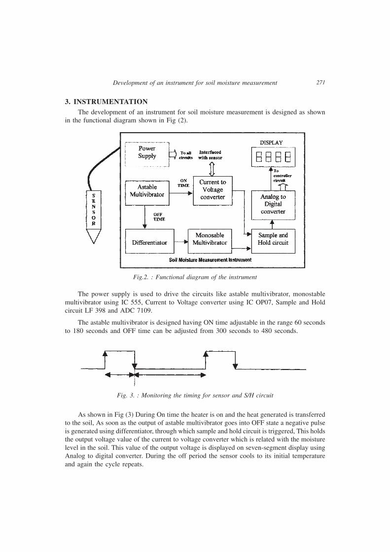
3. INSTRUMENTATIONThe development of an instrument for soil moisture measurement is designed as shown
in the functional diagram shown in Fig (2).
The power supply is used to drive the circuits like astable multivibrator, monostablemultivibrator using IC 555, Current to Voltage converter using IC OP07, Sample and Holdcircuit LF 398 and ADC 7109.
The astable multivibrator is designed having ON time adjustable in the range 60 secondsto 180 seconds and OFF time can be adjusted from 300 seconds to 480 seconds.
Fig.2. : Functional diagram of the instrument
Fig. 3. : Monitoring the timing for sensor and S/H circuit
As shown in Fig (3) During On time the heater is on and the heat generated is transferredto the soil, As soon as the output of astable multivibrator goes into OFF state a negative pulseis generated using differentiator, through which sample and hold circuit is triggered, This holdsthe output voltage value of the current to voltage converter which is related with the moisturelevel in the soil. This value of the output voltage is displayed on seven-segment display usingAnalog to digital converter. During the off period the sensor cools to its initial temperatureand again the cycle repeats.
Development of an instrument for soil moisture measurement
272
The output from the Analog to digital converter is compared with comparator. Thecomparator is preset at a reference voltage level as per requirement of the irrigation controlsolenoid valve. Hence this instrument can be used in automatic irrigation system. The facilitiesare provided to the instrument to adjust the timings according to the different soil type, cropetc. The sensor is provided with four-pin connector. The back panel view of the instrumentis shown in fig (4).
Fig. 4. : The back panel view of the instrument
4. EXPERIMENTAL WORKIn the development of this instrument, a thermal conductivity model using “C” language
program is used to optimize the sensor. The program calculates the thermal conductivity fordifferent parameters such as heater parameters, type of metal, its mass and area, types of soilwith heat transfer rates are verified. Selections of the material of the rod, its dimension, typeand size of the heater are chosen using software model, so as to suit for measuring soil moisturein shortest possible time. The Heat transferred is measured by using transient heat flow, whichis considered more accurate than steady state method. Transient methods minimize effects ofwater movement due to temperature gradients and do not require long time for the temperaturegradient to stabilize.
Referring the gravimetric method uses the soil samples used in calibration of theinstrument. To measure soil moisture, first the complete dry soil[3][4] is prepared. 120 gm ofsoil is heated at 105°C for 24 hours. Weighing and drying repeatedly in oven up to.
1 gm accuracy confirmed the dryness. The soil is kept in desiccators so as to protect itfrom humidity. Then 100 gm of the dry soil is taken into sample pot, which is used as 0%soil moisture level sample. The sensor is dipped into it to measure moisture level. Repetativeobservations are taken ten times for the same moisture level. Then by adding 10 ml of water
S.R. Chaudhari, S.A. Deuskar and A.D. Shaligram
273
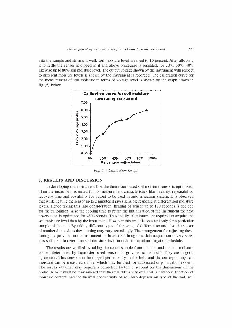
into the sample and stirring it well, soil moisture level is raised to 10 percent. After allowingit to settle the sensor is dipped in it and above procedure is repeated. for 20%, 30%, 40%likewise up to 80% soil moisture level. The output voltage shown by the instrument with respectto different moisture levels is shown by the instrument is recorded. The calibration curve forthe measurement of soil moisture m terms of voltage level is shown by the graph drawn infig (5) below.
5. RESULTS AND DISCUSSIONIn developing this instrument first the thermister based soil moisture sensor is optimized.
Then the instrument is tested for its measurement characteristics like linearity, repeatability,recovery time and possibility for output to be used in auto irrigation system. It is observedthat while heating the sensor up to 2 minutes it gives sensible response at different soil moisturelevels. Hence taking this into consideration, heating of sensor up to 120 seconds is decidedfor the calibration. Also the cooling time to retain the initialization of the instrument for nextobservation is optimized for 480 seconds. Thus totally 10 minutes are required to acquire thesoil moisture level data by the instrument. However this result is obtained only for a particularsample of the soil. By taking different types of the soils, of different texture also the sensorof another dimensions these timing may vary accordingly. The arrangement for adjusting thesetiming are provided in the instrument on backside. Though the data acquisition is very slow,it is sufficient to determine soil moisture level in order to maintain irrigation schedule.
The results are verified by taking the actual sample from the soil, and the soil moisturecontent determined by thermister based sensor and gravimetric method[5], They are in goodagreement. This sensor can be dipped permanently in the field and the corresponding soilmoisture can be measured online, which may be used for automated drip irrigation system.The results obtained may require a correction factor to account for the dimensions of theprobe. Also it must be remembered that thermal diffusivity of a soil is parabolic function ofmoisture content, and the thermal conductivity of soil also depends on type of the sod, soil
Fig. 5. : Calibration Graph
Development of an instrument for soil moisture measurement
274
texture, organic matters in soil and compaction of soil molecules. Hence the calibration formoisture measurement sensor may be slightly modified according to these parameters relatedto the soil properties.
REFERENCES1. S.R. Chaudhari, S.A. Deuskar and A.D. Shaliyram,* Paper presented at NSAI 2001, Chandigarh.
*(Development of thermister based soil moisture meter for use in mobile weather station”).
2. J.P. Holman, “Heat Transfer S I METRIC EDITION ”, McGraw Hill publications. (1989)PP 1-14.
3. N.L Bote and V.B. Vaidya, “Measurement of soil moisture”, Center of Advanced studies inAgricultural Meteorology, College of Agriculture, Pune- 5. (1997)
4. Prof. N.L, Bote, “Soil Moisture and its Measurement”, Center of Advanced studies inAgricultural Meteorology, College of Agriculture, and Pune-5. (1997)
5. Web site: http://www.eosdis.ornl.gov/FIFE/Dataset Soil Moisture Gravimetric Data.html “FIFESoil moisture Gravimetric Data Set Guide Document.”
S.R. Chaudhari, S.A. Deuskar and A.D. Shaligram
275
A PERSONAL DOSIMETER READER SYSTEM FORNUCLEAR EMERGENCIES
A. S. Rathore, D. K. Gupta, Manish Mishra, Anil Goyal, H. C. Samaria,and R. L. Chouhan
Defence Laboratory, Jodhpur-342011
ABSTRACT
The existence of Nuclear weapons presents military commanders with vast problems.The main worry of the commander is to know the radiation exposure status of the unitunder his command. The RPL Dosimeter Reader system enables the commander to knowthe radiation exposure status of the unit members. This is a portable instrument capableof measuring Gamma and Neutron radiation doses registered by a personal dosimeterworn on wrist by combat unit members during nuclear emergencies. The dosimeter is asmall unit containing RPL glass and PIN diode for Gamma and Neutron doses respectively.
This unit enables the commander to assess the dose received by the unit under hiscommand and to incorporate this information in to overall planning. The locket worn byeach member of the combat group records the radiation dose and keeps the informationsecret, This instrument is simple to operate and working with a single 12V dc battery.
1. INTRODUCTIONThere are four types of radiation that can be considered as an outcome of Nuclear weapon
i.e. alpha, beta, gamma and neutron radiations. From military stand point alpha and betaradiations can be regarded as contaminant category and effect can be reduced by a respiratorand purposely designed clothing whereas gamma and neutron radiations are penetrating radiationbecomes the major hazard. The wrist watch concept gives the convenient method of wearingdosimeter which can be incorporated with sensors RPL glass and PIN diode for Gamma andNeutron doses respectively.
A personal dosimeter reader system has been developed for measuring gamma and neutronradiations registered by a watch type personal dosimeter, the Reader system has been developedindigenously. This instrument displays the Neutron radiation dose and the total dose i.e.summation of Neutron and Gamma radiation dose. This instrument has been accepted forintroduction into services after environmental testings as per the Table L2 of JSS 55555 [7].This paper describes the design details of the dosimeter reader system.
2. PRINCIPLE OF OPERATIONThe dosimeter is a passive, small, light weight unit containing two sensors viz. a RPL
glass and a PIN diode for the recording of Gamma and Neutron radiation doses respectively.
J. Instrum. Soc. India 32 (4) 275 - 279
276
The Gamma radiation detection is accomplished using specially produced Silver activatedPhosphate Glass which exhibits a property known as Radiophotoluminescence. This is thecreation of luminescence centre in the glass (by the action of X-ray or Gamma ray) whichsubsequently be excited by ultraviolet light to produce the orange light emission. Without X-ray or gamma ray irradiation the light emitted is purple and can be readily differentiated fromradiophotoluminescent light by optical filtering. The radiophotoluminescence is proportionalto the radiation dose up to 1200 cGy. Received doses are additive and are independent ofdose rate or direction.
The Neutron radiation detection is accomplished by a specially developed silicon PINoperating in high current density region[1]. This is a wide base silicon PIN diode operating inrelatively high current density so that conductivity of base region is determined by the densityof injected charge carners. This density is a function of carrier diffusion length (L), which isdependent on carrier life time. Thus L= % (TD) where D is diffusion constant. The densityof injected charge carrier is a function of the L which is dependent on carrier life time T.Exposure to fast neutron creates lattice vacancies and interstitial atoms within the crystal latticegiving additional recombination centres which reduces the lifetime of carriers in the base region.This decreases the carrier diffusion length and hence the carrier density for a given appliedvoltage[2]. If a constant current is passed through the diode in forward direction, the resultof fast neutron irradiation leads to an increase of forward voltage which can be used todetermine the dose received.
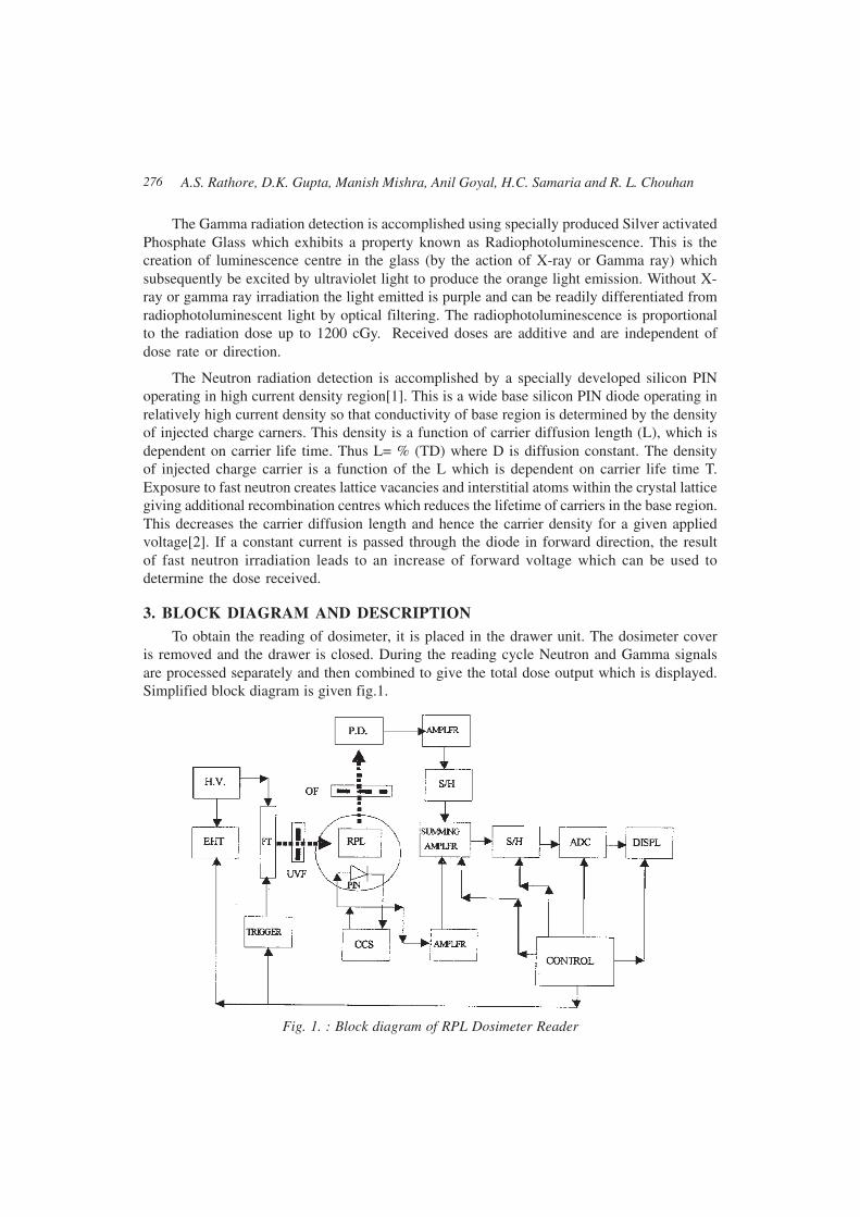
3. BLOCK DIAGRAM AND DESCRIPTIONTo obtain the reading of dosimeter, it is placed in the drawer unit. The dosimeter cover
is removed and the drawer is closed. During the reading cycle Neutron and Gamma signalsare processed separately and then combined to give the total dose output which is displayed.Simplified block diagram is given fig.1.
Fig. 1. : Block diagram of RPL Dosimeter Reader
A.S. Rathore, D.K. Gupta, Manish Mishra, Anil Goyal, H.C. Samaria and R. L. Chouhan
277
In the Gamma channel the nondestructive reading is accomplished by illuminating oneedge of the RPL glass with Ultra Violet light and measuring resultant luminescence emittedfrom the upper face of glass. A short pulse of UV light is selected from the light spectrum ofxenon flash lamp by ultra-violet pass filter. The energy of 2.8 joules approx. required by flashlamp is stored in capacitor situated in the flash unit. The unit also houses a circuitry whichtriggers the flash tube. The orange luminescence emitted from the glass is selected by suitablepass filter and presented to photodiode in the gamma channel. The silicon photodiode convertslight signals into electrical current which is fed to low impedance input of gamma amplifier.The gamma channel integrates the photodiode current and produces a peak output voltagewhich is proportional to gamma dose. This out put is fed to the sample and hold circuit in themain amplifier for further processing. The gain of the main amplifier is independently adjustableto allow to compensate temperature coefficients of gamma glass & neutron diode. Thecalibration of gamma channel is done by radiation hardened glass to give a predetermined dosereading.
In the N- channel the reading of diode is accomplished by supplying a pulse of 100 mAcurrent for 4 mSec and measuring the forward voltage drop. The offset voltage is set by astandard zero neutron PIN diode. The diode forward voltage is amplified by N- amplifier andfed to main amplifier and it is summed with gamma signal and then displayed. The gain of N-channel amplifier is set by another standard pin diode during calibration. The final combinedsignal is stored for a short duration in main amplifier A, during this period a sample is takenby display unit, which displays the reading for 20 Secs.
4. ELECTRONIC SUBSYSTEMSThe system operation is achieved by number of operational amplifiers and CMOS ICs.
Five printed circuits boards are designed to meet the performance requirement of the equipment.The printed circuit boards can be categorised as follows:
4.1 - Trigger CircuitIt is housed at upper portion of the instrument which takes the input from front panel
switches and generates various trigger signals for constant current source, sample and holdfor neutron, gamma and summing amplifier, flash trigger, display ON period etc.
4.2 - Control and Hold Amplifier CircuitThis unit works in accordance with the signals from trigger circuit and generates output
for display. The neutron dose and gamma dose signals are amplified. A summingamplifier and hold circuits are provided in this card to give the output voltage proportional tothe radiation doses.
4.3 - EHT CircuitThis circuit is located at rear bottom portion of the instrument housed in a steel casing
and generates 1000 to 1300V I3C approx. to charge the energy storage capacitor for flashtube operation.
A Personal Dosimeter Reader System for Nuclear Emergencies
278
4.4 - Flash CircuitIt receives trigger signal from trigger circuit and discharges the electrical energy of the
capacitor through the flash tube to generate UV flash.
4.5 - Display circuitThis circuit consist of CMOS ICs and seven segment display to form a digital panel meter
and located at the front panel. The voltage corresponding to neutron and gamma signal isconverted to digital signal and displayed.
5. CONSTRUCTIONAL DETAILSThe RPL Dosimeter reader is made of Die cast aluminium body. A cover is provided at
the front panel which can be opened / closed by screws. All the operating switches and visualdisplays are located at the front panel except the power supply connector, ON/OFF switchand fuse are at the rear side of the instrument. A moveable drawer has been provided at thefront panel to house the dosimeter locket which can be guided and aligned into the equipmentto take the measurement of the doses received by the lockets. Dimensions of the readeris 425 mm X 250 mm X 300 mm and weight is approximately 15 Kg.
6. MEASUREMENT AND METHODThe reader is calibrated with the help of reference locket and front panel controls. A set
of personal dosimeters with different gamma and neutron dose values ranging from low tohigh is taken. These dosimeters are read on the reader unit. A plot between the actual doseand the measured dose is shown in the fig.2. The accuracy of the reading was found to bewithin ± 10% which is good enough for any radiation measurement instrument.
Fig. 2. : A plot between the actual dose and the measured dose
A.S. Rathore, D.K. Gupta, Manish Mishra, Anil Goyal, H.C. Samaria and R. L. Chouhan
279
7. CONCLUSIONThe indigenously developed RPL dosimeter reader is a very useful nuclear instrument
for the measurement of neutron and gamma radiation accumulated in the dosimeter in therange 1 - 1200 Rads and has fulfilled the requirement of Indian Army. The dosimeter is issuedto every individual soldier working in contaminated area during nuclear emergencies and thereader is kept in the base unit. The locket is read on the reader and the dose record is maintainedfor every individual. The soldier will not come to know his dose record however the commanderof the unit will be knowing the doses taken by every individual which helps in avoiding anycasualty. The instrument is indigenously designed and developed except three criticalcomponents. This development in India will be a support to the national technologicalindependence.
ACKNOWLEDGEMENTThe authors would like to thank Sh. R. K. Syal, Director Defence Laboratory, Jodhpur,
Dr. M. P. Chacharkar, Head, Isotope Division for support and encouragement during the work.The authors also express their sincere thanks to Dr. A R. Reddy, former Director Defencelaboratory, Jodhpur and Sh. P. K. Bhatnagar, Jt. Director, Defence laboratory, Jodhpur for hishelp and guidance throughout the development the RPL Dosimeter Reader. We are also thankfulto production agency Instrumentation Limited, Kota for sincere efforts in developing theinstrument.
REFERENCES1. P.K. Bhatnagar, “Fast neutrons irradiation for fabrication of narrow forward voltage p-i-n
diodes”, Nucl. Instr. And Meth. in phy. A329 (1993)
3. G.C. Messenger and M.S. Ash, “The effects of Radiation on Electronic systems” Van NostradReinfold, New York, 1986
4. W. Shockley, Electrons and holes in the semiconductors (Van Nostrad Reinfold, New York,1950)
5. Glen F. Knoll, “Radiation detection and measurements”, John Willey & Sons, 1979
6. Jacob Millman, “Microelectronics”, McGraw International editions, 1988
7. Joint Services Specifications JSS 55555 “Environmental test methods for Electronic andElectrical Equipment” Directorate of standardisation, Ministry of Defence, 1977.
A Personal Dosimeter Reader System for Nuclear Emergencies
280
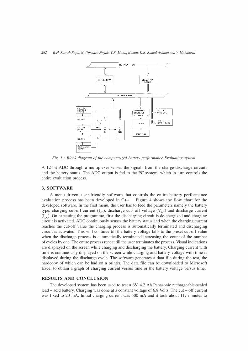
COMPUTERISED BATTERY PERFORMANCEEVALUATOR FOR SEALED MAINTENANCE FREE
LEAD-ACID BATTERIES
R.H. Suresh Bapu, N. Upendra Nayak, T.K. Manoj Kumar,K.R. Ramakrishnan and Y. Mahadeva
Electrochemical Research Institute, Karaikudi – 630 006
ABSTRACT
A computerized on-line battery performance evaluator has been designed and developed.It mainly consists of charge – discharge circuits and an interfacing add – on card. Thesystem has been used to evaluate 6V, 4.2 Ah maintenance free lead – acid battery. Thedesign aspects of the system and the results obtained are presented in this paper.
1. INTRODUCTIONCharge – discharge characteristics of a battery determine its quality. These characteristics
have also been used to evaluate the additives in the plates of lead – acid batteries1. Charge –discharge modules with different power capacities have been used to test the lead – acidbatteries and plate additives for various applications2-5. Nowadays maintenance free lead – acidbatteries have become prominent for various applications such as in industrial electronics,automobiles, entertainment electronics etc. The standard method of evaluating them is to chargethe battery at constant voltage till the current falls to preset cut – off value and discharge ata constant current till the voltage reaches the critical cut- off value. This forms a single cycle.The number of such cycles depend on the quality of the battery, more the number better thelife of the battery. In this paper a computerized battery performance evaluator for maintenancefree lead – acid batteries has been discussed.
2. HARDWAREThe battery performance evaluator system mainly consists of a charging circuit, a
discharging circuit, PC – add on card and a personal computer system.
2.1 Battery Charging CircuitFigure 1 shows the block diagram of the battery charging circuit. It mainly consists of
a Digital to Analog converter (DAC), amplifier circuits, a sense resistor and a multiplexer.Charging, is carried out at a constant voltage till the charging current falls to the cut-off valuewhen the charging circuit is de-activated. Constant charging voltage is generated using a 12
J. Instrum. Soc. India 32 (4) 280 - 284
281
– bit DAC. As the maximum output of the DAC is only 5V, it is further amplified to the requiredvoltage with the D.C amplifier. The gain of the D.C amplifier is set depending on the voltagerating of the battery to be charged. This voltage is fed to a power amplifier, which has beendesigned to give a maximum current of 5 Amps. The output from the power amplifier chargesthe battery under test. A sense resistor in series with the battery senses the charging current.A differential amplifier amplifies the voltage drop across the sense resistor and outputs it to amultiplexer. The multiplexer output is sensed by the PC through an Analog to Digital converter(ADC) and the DAC is de-activated when the charging current reaches the cut-off value.
2.2 Battery Discharging Circuit
Fig. 1. : Block diagram of the battery charging circuit
Figure 2 shows the block diagram of the battery discharging circuit. It consists of anotherDAC, a d.c.electronic load, battery under test, an attenuator and a multiplexer. The battery isdischarged under constant current and when its voltage falls to cut-off value, discharging isterminated. An electronic module has been designed to act as a load, which discharges thebattery under test at a constant current. While in discharge, the battery voltage is sensed bythe multiplexer through an attenuator connected to the battery. When the battery voltage fallsto the preset cut-off value, the DAC is de-activated terminating the discharging process.
Figure 3 shows the detailed block diagram of the computerized battery performanceevaluating system. The signals from and to the battery charge – discharge module are interfacedto PC using an add-on card. The PC add-on card consists of two 12-bit DACs, oneProgrammable Peripheral Interface (PPI), one 12-bit ADC and a multiplexer. DACs 1 and 2feed the initial voltages to the charging and discharging modules respectively. Depending onthe preset logic the I/O lines of the PPI activate the driver circuits, which in turn energize therelays 1 and 2. Relays 1 and 2 activate the battery charging and discharging circuits respectively:
Fig. 2. : Block diagram of the battery discharging circuit
Computerised Battery Performance Evaluator for sealed maintenance free Lead-Acid Batteries
282
A 12-bit ADC through a multiplexer senses the signals from the charge-discharge circuitsand the battery status. The ADC output is fed to the PC system, which in turn controls theentire evaluation process.
3. SOFTWAREA menu driven, user-friendly software that controls the entire battery performance
evaluation process has been developed in C++. Figure 4 shows the flow chart for thedeveloped software. In the first menu, the user has to feed the parameters namely the batterytype, charging cut-off current (I
CC), discharge cut- off voltage (V
DC) and discharge current
(IDC). On executing the programme, first the discharging circuit is de-energized and chargingcircuit is activated. ADC continuously senses the battery status and when the charging currentreaches the cut-off value the charging process is automatically terminated and dischargingcircuit is activated. This will continue till the battery voltage falls to the preset cut-off valuewhen the discharge process is automatically terminated increasing the count of the numberof cycles by one. The entire process repeat till the user terminates the process. Visual indicationsare displayed on the screen while charging and discharging the battery. Charging current withtime is continuously displayed on the screen while charging and battery voltage with time isdisplayed during the discharge cycle. The software generates a data file during the test, thehardcopy of which can be had on a printer. The data file can be downloaded to MicrosoftExcel to obtain a graph of charging current versus time or the battery voltage versus time.
RESULTS AND CONCLUSIONThe developed system has been used to test a 6V, 4.2 Ah Panasonic rechargeable-sealed
lead – acid battery. Charging was done at a constant voltage of 6.8 Volts. The cut – off currentwas fixed to 20 mA. Initial charging current was 500 mA and it took about 117 minutes to
Fig. 3 : Block diagram of the computerized battery performance Evaluating system
R.H. Suresh Bapu, N. Upendra Nayak, T.K. Manoj Kumar, K.R. Ramakrishnan and Y. Mahadeva
283
Fig. 5 : Charging characteristics of a 6V 4.2Ah rechargeable sealed lead acid battery
reach the current cut – off value. Figure 5 shows the variation of charging current with time.The discharging current was fixed to 0.1C i.e. 420 mA and the voltage cut-off was fixed at6.25 Volts. Battery had an initial voltage of 6.56 Volts and decreased to the cut – off value inabout 47 minutes. Figure 6 shows the variation of battery voltage with respect to time duringdischarge cycle. These results indicate that the system works satisfactorily. So the systemgives not only the number of cycles but also the charge, discharge characteristics with respect
Fig. 6 : Discharging characteristics of a 6V4.2 Ah rechargeable sealed lead acid battery
Fig. 4 : Flow chart of the developed system
Computerised Battery Performance Evaluator for sealed maintenance free Lead-Acid Batteries
284
to time. The developed battery performance evaluator can be used to test the maintenancefree lead-acid batteries of 2, 6 and 12 volts rating with different ampere-hour capacities.
REFERENCES1. R.Flores, L.M. Blanco “Electrochemical evaluation of additives for lead – acid batteries under
high-discharge condition”, Journal of Power Sources 78, 30 – 34 (1999)
2. R.C. Bharadwaj “Constant & pulse power capabilities of lead – acid batteries made with thinmetal films for different application” Journal of Power Sources 78, 130 – 138 (1999)
3. T.G. Chang, D.M. Jochim “Structural changes of active materials and failure mode of avalue regulated lead – acid battery in rapid – charge and conventional charge cycling. Ibid.91, 177 – 192 (2000)
4. D. Paulov, G. Petkova, M. Dimitrov, M Shiormi, M. Isubota ”Influence of fast charge on thelife cycle of positive lead – acid battery plates” Ibid. 87, 39-56 (2000)
5. M. Dimitrov, D. Paulov “Influence of grid alloy and fast charge on battery cycle life andstructure of the active mass of lead – acid batteries” Journal of Power sources 93, 234 – 257(2001).
R.H. Suresh Bapu, N. Upendra Nayak, T.K. Manoj Kumar, K.R. Ramakrishnan and Y. Mahadeva
285
GRAPHICAL PRESENTATION OF DATA ACQUIREDTHROUGH DATA ACQUISITION SYSTEM,
USING LCD MODULE
A.K. Pansare*, M.T. Tipugade* and A.M. Narsale***Western Regional Instrumentation Centre, Mumbai - 400098
**Dept. of Physics, Univ. of Mumbai, Mumbai - 400098
ABSTRACT
Liquid crystal display graphics modules are being increasingly used in the presentationof data in graphical format. The conventional alphanumeric LCD modules are not suitablefor display of high resolution graphical information; they can only be used to displayalphanumeric characters and character graphics. The LCD graphics module overcomesthis limitation of the conventional LCD modules. Using these modules the informationcan be displayed both in graphical format and as alphanumeric characters.
In the present application to display particle size analysis information, it was necessaryto display the results acquired through the data acquisition system in a graphical manner.The results after suitable data processing can be presented in tabular, x-y graph or bar-graph format. The microcontroller software is user friendly and enables the easy selectionof the format for display. The software also permits to enter the experimental parametersand displays these on the LCD module. The experimental conditions can also bedisplayed. The paper discusses the design features, and algorithms used for the displayof data in various formats.
1. INTRODUCTIONThe use of liquid crystal display for presentation of data had been so far restricted to the
use of alphanumeric LCD modules. However, with the easy availability of LCD graphicsmodules, they are being increasingly used for presentation of data in graphical format. Theconventional alphanumeric LCD modules are not suitable for display of high resolution graphicalinformation and can only be used to display alphanumeric characters and character graphics.The LCD graphics module overcomes this limitation of the conventional LCD modules. Usingthese modules, the data and information can be displayed both in graphical format and asalphanumeric characters.
2. FEATURES OF THE LCD MODULEThe Graphic LCD Module (1), from M/s Oriole, consists of LCD panel with CMOS LSI
integrated circuits for LCD driving. The module has full dot matrix graphic display and has amatrix of 240 x 128 dots. It is possible to display graphics as well as characters; thus, numerics,alphabets, special characters, graphs, charts and patterns etc. can easily be displayed. It has
J. Instrum. Soc. India 32 (4) 285 - 289
286
high contrast and wide viewing range. The number of dots are arranged as a matrix of240 x 128 dots and the viewing area is 114mm (w) x 64 mm (h), with dot size of 0.4 mm x0.4 mm and dot pitch of 0.45 x 0.45 mm. The overall module size is 133 mm x 79 mmapproximately.
2.1 Interfacing and communication of the LCD module with the controllerHardware interfacing of LCD module with the 8051 family microcontroller (1,2) is done
by appropriately connecting the module control lines to the microcontroller. The register selectline is tied to address AO, the read/write line is connected to the write line and the data busis connected to the data bus of the controller. The chip select, reset and the enable signal arealso appropriately tied to the respective outputs from the microcontroller. The block diagramof the hardware interfacing is shown in figure 1.
Fig. 1 : Block diagram of the hardware interfacing
To have effective communication between the module and the microcontroller, it isnecessary to write a software which will correctly initialize the various registers of the module.The display is controlled by writing data into the instruction register and 13 data registers.The RS signal distinguishes the instruction register from the data registers. Address of thedata register is written into the instruction register with RS=1. After that, the 8-bit data iswritten in the data register and the specified instruction is executed with RS=0. During theexecution of the instruction, no new instruction can be accepted. Since the busy flag is setduring this operation, the busy flag is read and it is ensured that the busy flag is zero beforewriting the next instruction.
The module control software consists of having a control sequence using the variousinstructions, such as the mode control, setting of the character pitch, number of characters,number of time divisions, low and high order addresses, writing and reading of data, etc. Theflow chart of the initialization sequence for use in character mode is given in figure 3, whereasthe flow chart of the initialization sequence for use in the graphic mode is given in figure 4.
2.2 Software DescriptionThe software to display the graphics consists of modular routines to perform the various
functions such as initialization of the LCD module and the display of data in the selected format.The modular routines can be broadly classified as follows:
A.K. Pansare, M.T. Tipugade and A.M. Narsale
287
i) Software routines for initialization of the LCD module
ii) Software routines for selection of the choice of the display format
iii) Software routines for displaying the data, from the memory, in the selected format
iv) Software routines for overall control of the LCD module for displaying the correctformat.
Figure 2 gives the flowchart for the software for displaying the data in the selected format,whereas the flow charts for the initialization and control of the LCD module, in the appropriatemodes, are shown on figures 3 and 4.
Fig. 2. : Flow Chart for displaying data in selected format
Graphical presentation of data acquired through Data Acquisition System, using LCD module
288
2.3 Data Presentation FormatsThe acquired data is stored in the memory and is available for off-line display. For the
current application, the options available for the presentation formats that can be selected are:
i) Tabulation
ii) Point graph
iii) Bar graph
After the choice is made, the presentation of data is carried out by selecting the appropriatesoftware routine. Tabular presentation essentially uses the (character) alphanumeric mode fordata display, whereas point graph and bar graph presentations require the use of the graphicsmode. However, the present software has been designed to display the data only after thecompletion of data acquisition.
Fig. 3. : Control Sequence - Character Mode
A.K. Pansare, M.T. Tipugade and A.M. Narsale
289
3. CONCLUSIONSThe presentation of data acquired through a data acquisition system has been done on a
graphic LCD display. The use of microcontroller of 8051 family has been made for hardwareinterfacing of the LCD graphics module. The modular software structure has been used forprogramming the LCD module appropriately for displaying the selected presentation format.This feature will enable subsequent modifications/additions to the software to be carried outwith minimum effort.
The software for LCD graphics is being suitably modified so that it can be used to displaythe information/results obtained from any other instrument. Only the modular software routinesfor that particular application need to be changed to fulfill the requirements. Also, with slightmodification in the software, it is possible to display the data in real-time. The modificationsto this effect are in progress.
2. The 8051 Microcontroller – Kenneth J. Ayala, 2nd Edition, 1996, Penram InternationalPublishing (India).
Fig. 4. : Control Sequence - Graphic Mode
Graphical presentation of data acquired through Data Acquisition System, using LCD module
290
SPIRAL COIL MICROBEND FIBER OPTIC SENSOR
A.K. SinghInstrumentation Lab, G M Faculty, Institute of Armament Technology, Oirinagar
Pune- 411 025 (M.S.)
ABSTRACT
In the present endeavour a typical microbend spiral coil fiber optic sensor has beenpresented. The design principle of spiral fiber microbend sensor has been discussed inthe paper. The effect of spiral parameters such as radius, pitch, number of turns of spiral,on sensor characteristics have been analyzed theoretically and experimentally.
1. INTRODUCTIONFiber optic microbend sensor is a simple and inexpensive intensity modulation sensor,
which can detect deformation and its various related parameters like strain, pressure,temperature, etc. It is a light intensity sensor(intrinsic) and the light intensity decreases withmechanical bending. Though, microbend losses have always been a cause of concern. forcable designer, the same microbend loss effects have been utilized in microbend sensors. Inpest a large number of studies1-3 have been carried out on microbend sensors. Lagakos et al4
have done generic analysis for a microbend fiber optic sensor and recently a review paper onmicrobend sensing has been published by Berthhold5 . A fiber microbend sensor hascomplicated sensing performance dependent on the deformation of fiber and fiber parameters.When a fiber is subjected to axial deformations, mode coupling occurs between the guidedmodes and the cladding modes. The optical power coupled to the cladding modes is heavilyattenuated due to the plastic jacket surrounding the fiber, If these micro deformations or periodicmicrobends satisfy the phase matching condition and the mode field overlap integral is nonzero, then strong wavelength dependent losses are observed in the output spectra of the fiber.Generally, these microbends are induced on the fiber by placing it between two grooveddeformer plates, which have a periodic spatial structure. These plates act as a transducer totranslate any incident perturbation to a longitudinal spatial deformation on the fiber. Extensiveresearch has been carried out in the field of ‘V’ groove fiber sensor.
In microbend sensors, bending loss of different kinds of optical fiber geometries, likecircular ring, 8- like shape, sinusoidal geometry, etc., is of prime importance. Design of thesesensors, which is based on various geometries, needs optimization of geometry parameters:The purpose of present study is to develop a microbend fiber sensor having simple and definitesensing characteristics. Since microbend loss can be unambiguously treated only in case ofcircularly bent single mode fiber, a spiral form fiber microbend sensor has been presented.
J. Instrum. Soc. India 32 (4) 290 - 295
291
For this configuration of sensor, an application of deformation in the spiral axis, leads to uniformchange in the radius of the circularly bent fiber. The induced microbend loss has been analyzedboth experimentally, as well as theoretically.
2. THEORYSignal attenuation is one of the most important properties of an optical fiber. The basic
attenuation mechanism in a fiber are absorption, scattering and radiative losses of the opticalenergy. Absorption is related to the material of the fiber, whereas scattering is associated bothwith material of the fiber and with structural imperfections in the optical wave guide. Attenuationis due to radiative effects originating from perturbations (both microscopic and macroscopic)of the fiber geometry. Radiative losses occur whenever an optical fiber undergoes a bend offinite radius of curvature. Microscopic meandering of the fiber core axis is known as microbending. Micro bending introduces slight surface imperfections, which causes mode couplingbetween adjacent mode resulting in radiative losses, which is dependent on the amount ofapplied fiber deformation, the length of fiber, and the exact distribution of power among thedifferent modes. Microbending losses depends also on the wavelength and on the type of fiber.In fact, excessive microbending can create additional fiber losses but to an acceptable level.
An extensive theoretical analysis of curvature loss for bent optical fibers has been done3,6.Consider a spiral coil with pitch ‘P’ and coil radius ‘Rf’ as shown in the Fig. l. Fromgeometrical relationship, radius of curvature (uniform) of spiral is given as
If the spiral has a pitch number ‘n’, the spring height, i.e. gauge length, which is ofsensor is Lg = nP. In the analysis of losses, loss coefficient is of crucial importance. The losscoefficient depends upon various fiber parameters i.e. Bending radius of fiber, wavelength oflight passed, fiber parameters such as core radius, core refractive index, clad refractive indexand type of fiber, i.e., multimode, single mode, graded or step index and pitch of the spiral.For a given fiber all these parameters are fixed except one i.e. the bend radius.
The equation of loss coefficient also involves various modal parameters other than thosementioned above. The equation for loss coefficient for graded index fiber is
where C = -4*Rc * W3 �/ ( 3*a * V2 ). For a typical fiber(graded index fiber) of NA =0.27; n1 1.49; n2 = 1.465; a = 31.25mm and for laser source of wavelength = 632nm, thenormalized frequency, V = 2� a*NA/ � =83.884 and D, = NA/(2*n1
2 ) = 0.06081. The losscoefficient
LC = (121.798/(Rc ½)) * e –0.2176*RC .......... (5)
The output power is given by the equation,
Pout = Pin * e-LC*S*N .......... (6)
Thus, with change in the type fiber, the magnitude of loss coefficient will be different.
3. RESULTS AND DISCUSSIONIn the experimental setup, fiber is tightly wound around springs of different radii having
different numbers of turn. The light source is a He-Ne laser (l = 632nm ) to avoid undesirableinterference effects especially chromatic distortion. The power output is measured using apower meter. Fig.2-4 show the variation of P
out/P
in with number of turns of various values of
radius for fiber(graded index fiber). In these figures the output is normalized with referenceto input to reduce the error contribution due to light intensity changes caused by cable bending,light source fluctuations and connector losses. Following conclusions can be drawn from thesefigures: a) with increase in fiber radius increases, sensitivity increases and maximum outputdecreases; b) with increase in pitch increases, output decreases; c) for same value of pitchand former radius, output is higher for lesser number of turns and sensitivity is more forhigher number of turns.
Table 1-3 shows the variation of output power with weight for fixed values of formerradius and number of turns, varying from 5 to 7. The analysis of results shows that outputis an. inverse function of pitch. It is. apparent from the graphs that input and output have anapproximately linear relationship.
A.K. Singh
293
Fig
. 2
: Va
riat
ion
of N
orm
aliz
ed o
utpu
tw
ith
Num
ber
of t
urns
of
spir
al f
or v
ario
usva
lues
of
radi
us o
f cu
rvat
ure,
for
spi
ral
pitc
h of
4 m
m.
Fig
. 3
: Va
riat
ion
of N
orm
aliz
ed o
utpu
tw
ith
Num
ber
of t
urns
of
spir
al f
or v
ario
usva
lues
of
radi
us o
f cu
rvat
ure,
for
spi
ral
pitc
h of
6 m
m.
Fig
. 4:
Var
iati
on o
f N
orm
aliz
ed o
utpu
tw
ith
Num
ber
of t
urns
of
spir
al f
or v
ario
usva
lues
of
radi
us o
f cu
rvat
ure,
for
spi
ral
pitc
h of
8 m
m.
Spiral Coil Microbend Fiber Optic Sensor
294
Pout (�W)Weight (Kg)
N = 5 N = 6 N = 7
– 17.6 20.2 14. 7
0.5 15.9 19.5 14.1
1.0 14.28 19.3 13.7
1.5 12.0 19.1 13.3
Table 1: Variation of output power with weight for number of turns of fiber N= 5,6 and 7 andradius of curvature R
c=7.0 mm for fiber (Graded index fiber, NA 0.27).
Pout (mW)Weight (Kg)
N = 4 N = 5 N = 6
– 142.7 138.9 122.3
0.5 133.0 128.5 129.9
1.0 131.0 127.3 120.6
1.5 128.9 126.7 119.4
Table 2: Variation of output power with weight for number of turns N= 5,6,7 and radius ofcurvature Rc = 7.0 mm for fiber (step index fiber, NA 0.48).
Pout (mW)Weight (Kg)
N = 4 N = 5 N = 6
– 205 201 266
0.5 203 200 264
1.0 202 198 259
1.5 199 195 254
Table 3 : Variation of output power with weight for N=5,6,7 turns of fiber and radius ofcurvature R
c = 10.0 mm for fiber No. 2.
ACKNOWLEDGEMENTAuthor is thankful to director and Dean, Institute of Armament Technology, Girinagar,
Pune, M.S. (India) for granting permission to publish this work.
REFERENCES1 Vivek Arya, Kent A. Murphy, Anbo Wang, Richard O. Claus, Microbend Losses in Single
Mode Optical Fibers: Theoretical and Experimental Investigation, J. Light Wave Technol.,13(1995)1999-2002.
A.K. Singh
295
2. T. Yoshino, K. Inoue, Y. Kobayashi, Y. Takahashi, Spring Coil Fiber Microbend sensor withwell defined characteristics, Proceedings of 11th Optical Fiber Sensors Conference, Sapporo,1996.
3. R. C. Gauthier, C. Ross, Theoretical and Experimental Considerations for a Single Mode FiberOptic Bend Type Sensor, Appl. Opt. 36(1997) 6264-6273.
4. N. Lagakos, J H Cole and J A Bucaro, Microbend Fiber Optic Sensor, Appl. Opt. 26(1987)2171-2179.
5. J. W. Berthold III, Historical review of Microbend Fiber Optic Sensors, J Light Wave Tech.,13, 7 (1995) 1193.
6. T. Yoshino, K Inoue, Y Kobayashi, Spiral Fiber Microbend Sensors IEE Proc. Opto. Electron.,144(1997) 145-150.
Spiral Coil Microbend Fiber Optic Sensor
296
IMPLEMENTATION OF HOPFIELD NEURALNETWORK MODEL IN THE AREA OF
ASSOCIATIVE MEMORY
Jagdish Kumar1, Sandeep Kalra2 and Anil K. Chopra1
The human memory has its ability to learn about many new things without necessarilyforgetting them, learnt in the past. Exactly the same can be thought about the ArtificialNeural Networks system, How can its learning system remain responsive in response tosignificant input, yet remain stable in response to irrelevant input? How does the systemretain previously learnt information while continuing to learn about new information. Thispaper attempts to address the theory and implementation of Hopfield Neural Network inthe area of Associative Memory(AM). There are three types of Associative Memory:Hetero-associative Memory, Interpolative Memory and Auto-associative Memory. Humanmemory works on the basis of partial knowledge of its contents and or association withother information. This may be called as “Content-Addressible Memory”. We provide asmall part of input pattern to the system, the net or by self excitation the whole patternwill be regenerated. Neural network simulations have allowed researchers to study howand under what conditions such studies are that associative memory can do better inthe presence of a certain level of internal noise or with certain level of forgetfulness,The system, distributed as one memory is distributed over many synapses, superimposedbecause one synapse can be involved in several memories and robust because alteringa few synapses degrade the performance by very little.
1. INTRODUCTIONNeural networks are a highly promising, computational technology due to their capabilities
in mathematical modeling of human brain and solving complex problems approachable withtraditional methods such as statistical, pattern recognition and conventional artificial intelligence.The main attractive features of this paradigm are learning capability and parallel processing toachieve the results fast. Our memory works differently than traditional computers. Withtraditional computers, recall of information requires precise knowledge of the memory addressand a large part of database management is concerned with the handling of these addressese.g. in index files. However our memory works on the basis of partial knowledge of its contentand its association with other information [4].
J. Instrum. Soc. India 32 (4) 296 - 301
297
We have implemented the Hopfield Neural Network model in this paper as Hopfield NeuralNetworks form solvable models and analogies of brain activity. They provide some hard butsolvable puzzles and also represent dynamical systems most of the research in Hopfield networkshas been motivated by an interest in the dynamical or stochastic systems which Hopfield networkrepresents and an interest in the techniques that are used to solve them.
2. HOPFIELD NEURAL NETWORK
Hopfield Neural Network was firstly presented by Physics Scientist John Hopfield in 1982.It was inspired by the theory of magnetic field and memory mechanism of neural network; itplayed a vital role in the current resurgence of interest in the field of neural networks andeven used it to solve TSP (Traveling Salesman Problem) in 1985 successfully, his effortshave had a profound, simulated effect on the scientific community in the area of neuralnetworks.
We have tried to demonstrate how could Associative Memory be implemented [1,2]. Thememory is embedded in the strength of the numerous connections or synapses in the network.By suitably adjusting the strengths of all synapses using Hopfield learning technique, a netcan produce a pattern, when a suitable ‘clue’ [3] is provided.
Architecture and Theory of Hopfield Neural NetworkHopfield Neural Network has a single layer of neurons. Each node is fully interconnected
with every other node, via two way connections, allowing data to pass around in all thedirections. This network belongs to feedback network working with the mode of AssociativeMemory. Fig. (1) shows the architecture of discrete Hopfield Neural Network with fiveneurons each, each neuron, being a processing unit. Each processing unit has a activity valuethat is binary(0,1). The entire network is considered to have a “state” at each moment andthe state is a vector of 0’s or 1’s. Each entry in the vector corresponds to an individualprocessing unit in the network. Hence at any given instance, a state vector represents thestate of the network:
Ap = (ap,1,ap,2……………………..ap,n)=(u1-u2………….un)=(110010…)Where ap,i = i th entry in the pattern vector p.u1, u2, .......un are processing units having values 0/1.
Fig. 1 : Network has 5 nodes with states (0,1,0,0,1)
Implementation of Hopfield Neural Network Model in the area of Associative Memory
298
The processing units in the Hopfield network are fully interconnected, that is each unit isconnect to every other unit. The connections are directed (Fig.1).
In the associative memory application, the patterns to be stored as memories are chosena prior. The number of processing units in the network is equal to the number of entries inthe patterns to be stored.
Each interconnection has an interger weight associated with it. This weight is a scalarvalue, considered to be the connection strength. We denote Ti,j the weight to unit j from uniti. In the Hopefield network the weights Ti,j and Tj,i have the same value.
If there are m pattern in total A1………Am then
Initially, the network is assigned a state. Learning process is applied to the units in Hopfieldnetwork. Learning is the process of setting connection strength of the neurons. Once learningprocess is completed, the network can be presented with any test patterns. Now networkwill search for minimum energy state. Each neuron takes a weighted sum of its inputs andcalculates the output as shown in the Fig. 2. After calculating the sum, the processing unitthen evaluates whether the sum is greater or smaller than 0. If the sum is at lest 0, then outputof the unit is set at 1. If sum is less than 0, the output of unit is set as 0. The previous valueof a processing unit is not taken into account when it is updated. The updating procedureaffects the state of each processing unit, sometimes changing it sometimes leaving it the same.The updating procedure continues until no more changes can be made.
During the updating process each unit is selected one by one sequentially or randomlyuntil the network becomes stable, that is, all units retain the same value upon updating. In theupdating process posed by Hopfield the next unit to be updated is selected randomly. Sequentialupdate can become fruitless when there are different or equal probable stable states. The
Fig. 2 : Input and output of neuron
Jagdish Kumar, Sandeep Kalra and Anil K. Chopra
299
randomized updates used in the Hopfield Neural Network makes it unique among otherparadigms. In most of the neural network paradigms all the units in a single layer is updatedat the same time. In this aspect
Hopfield network is more close to the biological neuron models
in which neurons are updated in an unsynchronized manner.
Every state of the Hopfield network has an associated “energy” value, given by theequation.
The above function is known as the energy function/objective function that is to beminimized by the network. Updating procedure is nothing else than a systematic mechanismby which the energy of the overall network gets smaller and smaller. Finally the network goesinto a stable state, where all the energy is at a minimum. Now network state can be decodedand that will be the predicted pattern (output). It may be possible that the minima is local notglobal. In the Hopfield Network there is no way to reach the global minima from a local minima.It however can be restarted at a different initial position, which may allow the network tothen find global minima
Algorithm1. Set the weights o connection in the network. Strength of all connections are calculated
by the following equation.
2. Store the state of network and weights or connection strength between any two neurons.
3. Some test patterns that may contain the partial information of the stored patterns can beprovided input to the system.
4. Search for minimum energy state with this network state and do updations in the previousstate as according to fig.(2).
5. Repeat step 4. until network converges to a stable state.
6. Network state corresponding to stable state is then expected to respond to one of thememories of the network. Thus final stage matches to the stored memory that will bemost similar to the initial state.
ImplementationThe basic scheme behind the implementation is simple.
1. Each memory (string of information) is represented by a vector of 0/1. The informationis stored in a coded form. Each memory vector is a state of the network that corresponds
Implementation of Hopfield Neural Network Model in the area of Associative Memory
300
to a minimum in the space defined by the network energy. In our program we have taken100 processing units (neurons). Each character is converted to 5 bit binary code. Eachpattern is taken of 20 characters length.
2. Setting the connection strength of the network. Weights of all connections are decidedby learning process using Equation (1). We have taken two separate arrays of records(array and weight). The variable “array” is used to store the state of network and variable“weight” stores the connection strength between any two neurons.
3. The network is presented with test pattern that will contain the partial information of thestored pattern. Now the network will search for minimum energy state with this networkstate. Each time updating its previous state as according to Fig 2,the function of theupdating procedure is to move the state of the network from initial state of the networkuntil network converges to a stable state. Network state corresponding to that stable state,then is expected to correspond to one of the memories of the network. Thus the networkconverges to the stored memory that is most similar or most accessible to the initial state.
Its flow chart is shown in fig.3.
Fig. 3. Flow Chart
Jagdish Kumar, Sandeep Kalra and Anil K. Chopra
301
3. CONCLUSIONSIn spite of the fact that Hopfield Neural Network was a significant achievement, there
are still many limitations to its actual use.
1. The evoked memory is not necessarily the memory pattern that is most similar to theinput pattern.
2. All memories are not remembered with equal emphasis, some are evoked inappropriatelyoften.
3. If we present partial information up to 9 characters correctly out of 20, it convergessuccessfully in 90% cases.
Some-times the network evokes spurious states that are patterns that were not on theoriginal list of patterns to be stored as memories.
ACKNOWLEDGEMENTSThe authors are deeply grateful to Dr R.P. Bajpai, Director, CSIO,Chandigarh, Shri S.R
Taneja, Head, & Shri R.C.Gupta, Senior Scientist, Medical Electronics Instrument Division,CSIO,Chandigarh for their kind advice, encouragement and help during the progress of workand for permission to publish the same.
REFERENCES1. J.J. Hopfield, D.I Feinstein and R.G.Palmer: “Unlearning” has a stabilizing effect in collective
memories: Nature 304, 158 (1983).
2. J.J. hopfield and D.W Tank : Computing with Neural circuits: A Model, Science 233,625 (1986)
3. F. Crick : The recent Excitement about Neural Networks:Nature 337,129(1989)
4. B. Muller, Reinhardt: “Neural Networks-An Introduction” Springer Verlag.(1991)
5. Bogacz, R. (1996). Implementing Knowledge Database in Neural Network. In Proc. of the2nd Polish Conference on Neural Networks and Their Applications, 1 : 66-71.
6. Boz, O. (1997). Bibliography on Integration of Symbolism with Connectionism, and RuleIntegration and Extraction in Neural Networks.http://www.lehigh.edu/-ob00/integrated/re ferences-new.html.
7. http://www.generation5.org
8. Rafal Bogacz “BRAINN: A Connectionist Approach to Symbolic Reasoning”.
Implementation of Hopfield Neural Network Model in the area of Associative Memory
302
A COMPUTER INTERFACED OPTICALTHERMOMETER
B.B. Padhy and N. ChandrasekaranFaculty of Applied Physics, IAT (DRDO), Girinagar, Pune – 411 025
ABSTRACT
An optical thermometer using intensity modulation technique with optical fiber sensorhas been designed. This type of sensor can be used for measuring temperatures in hostileenvironments where conventional sensors fail. The simplicity in implementation and lesscomplex hardware makes these type of sensors very suitable for industrialinstrumentation, in controls and automation.
The test set up here uses a plastic fiber made of Polymethyl methacrylate and a regulatedheating arrangement for affecting desired temperature changes. This data is used forcalibration of the sensor. The sensor is tested and confirmed for a temperature range of27°C to 80°C with a sensitivity of 0.03?W/°C. A minimum of 0.2°C change in temperaturehas been detected by the set up. The test result is be remotely interfaced with a PCthrough a PCL-207 ADC to give on- line display of the measured temperatures. This isvery useful for application in industries, where regulated temperature effect is a must forensuring the normal and optimum functioning of the system.
1. INTRODUCTION
Optical techniques have played an important role in instrumentation and sensors, especiallyfor non-contact measurements. During the early studies on fiber optic telecommunication,the high sensitivity of optical fibers was noticed. Taking advantage of this exceptional sensitivityof fibers to external perturbation, efforts started to use optical fibers for sensing variousparameters1. Consequently, sensors were commercially available for measurement ofvarious parameters including temperature, pressure, strain, displacement, voltage, acceleration,flow rate, thickness, rotation rate, humidity, pH, particle size, chemical reactionrate, fluorescence and chemical concentration, refractive index, electric fields and magneticfields etc2.
A sensor is a device, which senses a change in environmental parameters. A fiberoptic sensor modifies the optical signal passing through it in a particular way to indicatethe measured parameter and its variation . The general configuration of a fiber optic sensor isgiven in figure l.
J. Instrum. Soc. India 32 (4) 302 - 307
303
There are many advantages of optical fiber sensors over the electrical sensors3. Theyare: Immunity to electromagnetic and radio frequency interference, Intrinsically safe in explosiveenvironments and chemically inert, Resistant to nuclear or other ionizing radiation, Insulationfrom high voltage and absence of ground loops, Sensing of normally inaccessible locationspossible, Remote sensing with low loss optical fiber telemetry possible, Low volume and lightweight, Plenty of raw material for the fibers, Commercially available suitable optical sourcesand detectors, Distributed sensing possible owing to the large bandwidth.
Although light modulation in optical fiber sensors can be described in a number of waysviz., light intensity, optical phase, polarization and wavelength (color), all optical systems finallydepend on the detection of optical intensity. In other words, since photo detectors are capableonly of detecting optical intensity, all the above-mentioned properties of light must finally bedetected as a variation in the light intensity1.
2. CLASSIFICATION OF SENSORSBased on the sensing zone, the fiber optic sensors may be classified as either extrinsic or
intrinsic type2,5. In the extrinsic type, the modulation takes place outside the fiber and thefiber acts only as a medium to convey the light to and from the sensor head. In the intrinsictype, the light is modulated within the fiber itself, in response to the physical parameter/perturbation. Optical fiber sensors can also be classified based on the sensing techniques.Common sensing techniques are based on Intensity modulation, Phase modulation(interferometric), Polarisation and wavelength modulation of the light. The first two are morepopular3. Between the two, the intensity modulated sensors enjoy certain advantages1 like:–their simple design and implementation, less complex signal processing, compatibility with themultimode fiber technology and commercially available sources and detectors. The phasemodulated sensors on the other hand, offer higher sensitivity while adding to cost andcomplexity6. Moreover, the extreme sensitivities of the order of 10-8 °C which are achievablewith interferometric methods are usually not required and one degree accuracies are generallyadequate7.
3. INTENSITY MODULATED SENSORSIntensity modulated sensors are the simplest and most widely studied in the field of optical
fiber sensors3,8. These sensors employ modulation of the amplitude of transmission in thesensing region of the fiber. The measurand in the form of a sinusoidal varying quantity
Fig. 1. : Schematic of a fiber-optic sensor.
A Computer Interfaced Optical Thermometer
304
modulates the intensity of the light transmitted through the sensor. The modulation envelopeis reflected in the voltage output from the detector, which upon calibration, is used to retrievemeasure of the measurand3.
The basic advantage of this technique is that, the intensity is directly measured, which isthe ultimate measurement done in any type of fiber optic sensor and the sensitivity is usuallyvery much acceptable. Apart from this, the technology is widely studied since it is simplerand thus results in rugged and reliable systems1,8. However, there are some limitations. Firstly,in low- frequency intensity based optical sensors, the received optical power and desiredbandwidths are usually such that the sensitivity of detection is principally limited by shot noise(because of the statistical nature of the rate of arrival of photons at the detector) andthermal noise4.
Thus, the minimum resolvable increment in the optical signal level is proportional to thesquare root of the rate of arrival of photons in the time interval 1/B. So if the modulationsignal from the sensor is small, the SNR is reduced4. Secondly, the intensity modulation basedsensors are not absolute devices and hence require calibration.
In spite of these limitations, intensity modulated fiber optic sensors find wide use insensing parameters like Temperature, Pressure, Displacement, Refractive-index and LiquidLevel etc2.
4. EXPERIMENTThe hardware used for the setup are: a semiconductor LED source at 850�m
wavelength, a plastic fiber of 1mm core diameter and numerical aperture approximately 0.5,a regulated heating arrangement for affecting temperature changes, a thermometer forcalibration, a PIN photo detector, Signal conditioning circuit, Amplifier, Analog-to-Digitalconversion card, Display.
The idea of using plastic fiber is mainly because of the reason that plastic fibers have athermal coefficient of expansion greater by 2 to 3 orders of magnitude than glass fibers. Also,plastic fibers have high numerical aperture and hence high acceptance angle. In addition, easymechanical handling makes it more useful3. The experiment is based on recording the changein output power from an optical fiber operating as an intrinsic sensor, which is subjected todifferent temperatures.
The experimental setup is as shown in figure 2.
B.B. Padhy and N. Chandrasekaran
305
The power at the source end is launched into the fiber using a proper coupling mechanism.The outer jacket of the fiber is removed. The sensing region of the fiber is immersed in awater bath, which is heated with a regulated voltage supply. The temperature to which thesensing region is subjected is monitored using a thermometer. The procedure is repeated forseveral times and observed sets of readings are found to be consistent.
5. RESULTSStarting from room temperature up to 80°C, the setup shows a variation in the output
power with increasing temperature. The process is observed with taking out the heating sourceand allowing the temperature to fall down. While cooling down, it is observed that the rate isslower than that of heating. The reason for this is mainly due to the fact that, water takesmore time to cool down compared to the time taken for getting heated. Figure.3 shows thevariation of loss in output power with increase in temperature.
Fig. 2. : Block Schematic of the Experimental Setup.
Fig. 3. : Loss of output power as a function of temperature
A Computer Interfaced Optical Thermometer
306
As seen in the figure 3, the loss increases with the increase in temperature to which thesensing region of the fiber is subjected under the present study. Figure 4 shows the variationof the normalized loss (LN) along the y-axis versus temperature.
From figure 3. given above, the response (a straight line) can be written as
Y = 0.381108x – 1.16705
Thus, the sensitivity, which is given by the ratio of change in power to the correspondingchange in temperature, is found to be
�P—— = 0.03 �W/°C�T
It may be noted that, for longer length of the fiber, the minute changes get magnifiedover the entire length and produces a measurable change, thus increasing the sensitivity8.
For a fixed power of the source, the calibration is done using a PCL-207 ADC card. Theoutput current from the detector after the signal conditioning and amplification drives the ADCcard. When the detector output is fed, the corresponding temperature is displayed on the PC.A minimum of 0.2° C change in temperature could be detected by the setup.
6. CONCLUSIONSThe present study based on the above setup indicates that the sensor has simple design
and implementation, less complex hardware, has low cost and is a rugged one which iscompatible with multimode fiber technology. Moreover, by performing direct intensitymeasurements, some complicated aspects like more fiber optic components and devices etc.has been kept away7. The authors would like to bring out the fact that the temperature range
Fig. 4. : Variation of normalized loss with temperature
B.B. Padhy and N. Chandrasekaran
307
measured here is small. Thus, for chemical plants or industrial uses, where high temperaturemeasurements are required, temperature sensors using glass fiber would be more suitable.Also, to increase the sensitivity, glass fibers along with interferometric techniques would bethe best. A longer length of plastic fiber can also increase the sensitivity. Further it is suggestedthat, for industries requiring controlled temperature effects, it would be appropriate to providea feedback controller for switching the voltage supply ON and OFF at the required temperaturelevels.
REFERENCESl. B. Culshaw, ‘Optical Fiber Sensing and Signal Processing’, Peter Peregrinus Ltd.
3. B.P.Pal, ‘Fiber Optics in Telecommunication and Sensor Systems’, Wiley Eastern Limited,Delhi (1992).
4 J. Dakin, B.Culshaw, ‘Optical Fiber Sensors: Systems and Applications’, Vol. 2, Artech House,Boston and London (1988).
5. J. Dakin, B. Culshaw, ‘Optical Fiber Sensors: Principles and Components’, Vol. 1, Artech House,Boston and London (1988).
6. R.Waynant, M.Ediger, ‘Electro-optics Handbook’, McGraw-Hill Inc. (1993).
7. T.G. Giallorenzi, J.A. Bucaro, A. Dandridge, G.H. Sigel, J.H.Cole, S.C. Rashleigh and R.G. Priest,‘Optical Fiber Sensor Technology’, IEEE transactions on microwave theory and techniques,Vol. MTT-30, No.4, 472-508 (Apr 1982).
8. S.K. Sarkar, ‘Optical Fibers and Fiber Optic Communication Systems’, S. Chand and Co. Ltd(1997).
A Computer Interfaced Optical Thermometer
308
DESIGN, FABRICATION AND PERFORMANCEOF A FIBER OPTIC FLOWMETER
FOR TRANSPARENT FLUIDS
Nahar Singh+ Subhash C. Jain+, Sanjeev Kumar#, Vijay Mohal§
V. Pandey† and A. K. Aggarwal ++Coherent Optics Division, Central Scientific Instruments Organisation, Sector 30,
Chandigarh-160020 (INDIA)§Micro Positioning Systems Division, Central Scientific Instruments Organisation,
Sector 30, Chandigarh-160020 (INDIA)#National Research and Technology Consortium, 15, Sector 3, Parwanoo – 173220 HP, (INDIA)
†Fluid Flow Laboratory, National Physical Laboratory, New Delhi-110012 (INDIA)
ABSTRACT
The concept, design, fabrication and experimental implementation of a fiber opticflowmeter for transparent fluids is reported. The device operates on the principle of lightintensity modulation due to angular misalignment of multimode optical fibers caused bydrag of a streamline flow. The working laboratory model of the flowmeter was tested ina water flow line and the performance studied was found to be satisfactory. It offers thepossibility for remote monitoring of flow of non-corrosive and transparent fluids in variousscientific and industrial applications.
1. INTRODUCTIONFlow is an important process parameter constituting about 25% of the process sensors.
It is a commonly measured quantity in diverse application areas such as marine, domestic,agriculture, process and nuclear industries and over the years, a wide variety of flow measuringtechniques & instruments based on different mechanisms were proposed. The conventionalflowmeters were mainly based on the principles of different pressure, vortex, shedding,magnetic, turbine, positive displacement, variable area, drag, ultrasonic, laser and open channeletc1-3. They suffer from several types of problems such as electrical noise, poor sensitivity &low SNR due to poor environmental ruggedness. One of the current techniques being exploitedfor overcoming these shortcomings has been the use of optical fibers which owing to theirseveral inherent technical features, are able to provide improved measurement range, sensitivity,ruggedness, wide operating temperature range, remote mounting capability, multiplexing ofdata from different sensors and protection against EMI/RFI4-6. Accordingly, a few fiber opticflow measurement techniques/instruments based on different design concepts have been
J. Instrum. Soc. India 32 (4) 308 - 314
309
investigated and developed 7-9. In the present flowmeter, two multimode optical fibers ofdifferent diameters have been used, one for guiding light emanating from a 850nm batteryoperated LED, to the point of sensing inside the fluid where light exits the fiber, and the otherfor collecting the modulated light to couple it further to a PIN photodetector linked to an opticalpowermeter.
2. PRINCIPLE OF OPERATIONThe basic principle of operation underlying this device is based on intensity modulation
of light due to angular misalignment between a movable transmitter fiber and a fixed detectorfiber caused by the fluid flow and is depicted schematically in Fig.l (a), while the graphicdefinition for such a misalignment is shown in Fig. 1 (b). This misalignment results in loss of
FIG. 1(a): Schematic of the Working Principle of Fiber Optic Flowmeter
FIG. 1(b): Graphic Definition of Angular Misalignment Between two Optical Fibers
Design, Fabrication and Performance of a Fiber Optic Flowmeter for Transparent Fluids
310
coupled power and the coupling efficiency decreases with rise in flow rates. The theoreticalrelationship between light coupling efficiency and angular misalignment for the case of twomultimode optical fibers as mentioned further were worked out by Dieter Opielka et al 10 usinggeometrical optics approach and making the following assumptions:
- The mode-power distribution in the misalignment plane (S) is uniform
- The optical fibers used are identical with an inhomogeneous refractive index profilerepresented by the expression
where n0 = refractive index at the centre of the fiber core,n1 = refractive index of the cladding,D = relative index difference,r = distance from the fiber axis,a = fiber core radius, andg = profile exponent.
- Leaky modes are neglected- With the exception of angular misalignment, all other alignments between the two fibers
are perfect
The power coupling efficiency after a tilt can be estimated by integrating over the solidangle and the area of overlap in the misalignment plane and is given by Eq.(2).
Where a is the angle between the planes passing through the two fiber end faces, qco isthe maximum aperture angle of the fibers in glass for r = 0.
For smaller tilt angles (e.g. sina/2 << sinqco) the following simple expression can resultfrom Eq.(2).
Again for small angles, the following simple expression results from Eq. (4)
�s = 1 - 4 sin�/2 sinco
. . . (5)
Nahar Singh, Subhash C. Jain, Sanjeev Kumar, Vijay Mohal, V. Pandey and A. K. Aggarwal
311
The above equations 2 to 5 for coupling efficiency due to angular misalignment arerepresented graphically in Fig.2 by curves (2) to (5) respectively. Further, a more flexible andmore accurate approach for predicting loss of coupling efficiency due to misalignment inmultimode and step-index fibers which also takes care of arbitrary energy distribution and theeffects of cladding and jacketing is given in Ref. 11
Fig. 2. Power Coupling Efficiency of Step-Index and Graded-Index Fibers as a Function of theNormalised Misalignment [10]
3. DESIGN AND FABRICATIONThe design schematic of the fiber optic flowmeter developed is indicated in Fig.3. The
device consists of a rectangular aluminium block with a concentric circular hole drilled along
Fig. 3. Design Schematic of the Fiber Optic Flowmeter
Design, Fabrication and Performance of a Fiber Optic Flowmeter for Transparent Fluids
312
its length. A suitable rectangular cut made on top of this block provides proper mounting toa precision x-y-z micropositioner fitted with a holder for guiding the transmitter fiber. On thebottom side of the block, a second holder is fixed in a circular hole coaxial with the rectangularcut, for guiding the detector fiber. The x-y-z micropositioner enables aligning of the transmitterfiber with the fixed detector fiber, while keeping a small gap between the two fiber end faces.The holder guiding the transmitter fiber has been so designed that its upper portion remainsstationary while the lower portion has a suitably hinged small cylindrical fiber guide whichswings freely with the drag exerted by the fluid. The design ensures that there is no torsionalmotion of the guide due to fluid flow. Transmitter fiber (50/125um) with a graded index profileand a large diameter detector fiber (200/600um) with a step index profile, have been used forrealising a wide measurement range. The developed fiber optic flowmeter is portable and canbe conveniently used for remote monitoring of flow under field conditions. Fig.4 shows thephotograph of the developed flowmeter while being tested .
4. PERFORMANCEPerformance evaluation of the flowmeter was carried out using a small scale water flow
line facility available at the National Physical Laboratory, New Delhi and depicted schematicallyin Fig.5. The device was installed in the flow line and water was allowed to flow down froman overhead tank gradually by opening valve 1, while valve 2 was kept closed to avoid anydamage to the hinge. Later on, valve-2 was opened slowly for filling the flowmeter body. Inorder to establish a relation between volume flow rate and the coupled output optical power,the time required to fill the desired volume of accumulator measuring tank was estimated andthe corresponding output optical power was measured using an optical powermeter. The outputvolume of the water to be filled in for varying time periods was fixed as one litre e.g. in the
Fig. 4. Photograph of the Fiber Optic Flowmeter Under Test
Nahar Singh, Subhash C. Jain, Sanjeev Kumar, Vijay Mohal, V. Pandey and A. K. Aggarwal
313
first instance, one litre of water was filled in 60 secs (volumetric flow rate is 1 litre/min.)employing the valve adjustment and the corresponding optical power output was recorded. Inthe next step, one litre of water was filled in 55 seconds e.g. volumetric flow rate was 1.09litre/min. and the corresponding optical power output was again recorded. This procedurewas repeated till the output optical power became quite low.
5. RESULTS AND DISCUSSIONThe flowmeter was calibrated by using water flow rates varied from 1 to 6 litres/min.
and the corresponding output optical power was recorded. These measurements were repeatedseveral times and a good performance was observed for the indicated flow rates. A typicalexperimental curve obtained between flow rates and coupled output optical power is indicated
Fig. 5. : Schematic of the Flow Testing Facility
Fig. 6. : Variation of Optical Power Coupling with Flow Rates.
in Fig.6. This curve has a good resemblance with the theoretically estimated curves for thecase of identical fibers indicated in Fig.2. The slight deviation of the experimental curve couldperhaps be attributed to the use of non-identical fibers with different refractive index profiles.The flowmeter could be employed for applications involving measurement of low level flowrates of transparent and non-corrosive fluids specially where remote monitoring is required.
There have been two types of limitations namely, that of the calibration system and ofthe flowmeter. Due to absence of provision for fine adjustments in the flow testing facility,
Design, Fabrication and Performance of a Fiber Optic Flowmeter for Transparent Fluids
314
the volumetric flow rate below 1 litre/min could not be attained and the lower limit of themeasurement range thus could not be ascertained. The measurement range realised could,however, be extended by using a large diameter and high numerical aperture detector fiber ascompared to transmitter fiber and or appropriate fiber bundles for realising an increased areaof overlap. The sensitivity of the device can be enhanced by introducing suitable designmodifications e.g. replacing the present cylindrical swinging fiber guide with one having a flatsurface which will experience an increased drag and minimising friction at the hinge. Theflowmeter can be employed for field measurements as the LED used is battery operated andthe transducer is portable. The battery operated LED has the added advantage of overcomingthe problem of source intensity fluctuations to a good extent. The flowmeter can be used formeasuring flow rates of clean, transparent and non-reactive liquids. However, the limitationof non-reactive liquids could be overcome by using transducer and fiber holders made fromnon-metals. The device may require periodic cleaning of the fiber endfaces and recalibrationdue to the possibility of contaminants being present in the liquids.
ACKNOWLEDGEMENTSThe authors are grateful to Dr. R P Bajpai, Director, CSIO for the motivation to carry
out this work and the kind permission to publish this paper. They are thankful to Dr. J NSom, Head, Fluid Flow Laboratory, National Physical Laboratory, New Delhi, for the helpand co-operation in carrying out the test and performance evaluation of the flowmeter. Theco-operation and help provided by Mr. A D Kaul, Mr. J K Chhabra, Mr. Sushil Kumar, Mr. DP Chhachhia and Mrs. Asha Kumar is thankfully acknowledged. Thanks are also due to Mrs.Madhu Mehta for typing the manuscript.
REFERENCES1. C. Johnson, ‘Process Control Instrumentation Technology’, Prentice Hall of India Pvt. Ltd.,
New Delhi (1996).
2. James E. Hardy and Francis R Ruppel, ‘Measurement and Instrumentation of Flow’,Encyclopedia of Applied Physics, VCH Publishers Inc, New York, 445 (1994)
3. Harsh Vardhan, ‘Measurement-Principles and Practices’, Macmillian India Ltd., Delhi (1993).
4. Eric Udd, ’Fiber Optic Sensors: An introduction for Engineers and Scientists’, John Wiley &Sons Inc., New York (1991).
5. Brian Culshaw and John Dakin, ‘Optical Fiber Sensors: Systems and Applications’, Vol.II,Artech House Inc., Massachusetts, USA (1989).
6. Brian Culshaw and John Dakin, ‘Optical Fiber Sensors: Principles and Components’ Vol.I,Artech House Inc, Massachusetts, USA (1988).
11. K.T. Taylor and B.L. Anderson, Opt. Engg., 34, No.12, 3471 (1995).
Nahar Singh, Subhash C. Jain, Sanjeev Kumar, Vijay Mohal, V. Pandey and A. K. Aggarwal
315
1. Place of Publication : Bangalore
2. Periodicity of Publication : Quarterly
3. Printer’s Name : S. Sridhar(Whether Citizen of India) Yes
Navbharath EnterprisesNo. 10, Sirur Park ‘B’ StreetSeshadripuramBangalore - 560 020
4. Publisher’s Name : Instrument Society of IndiaProf. S. Asokan, Gen secretary
(Whether Citizen of India) Yes
5. Editor’s Name : Prof. G. Mohan Rao(Whether Citizen of India) YesAddress Instrument Society of India
Dept. of InstrumentationIndian Institute of ScienceBangalore - 560 012
6. Name and address of individuals : Instrument Society of Indiawho own the Newspaper and partners Dept. of Instrumentationor shareholders holding more than Indian Institute of Scienceone percent of the total capital Bangalore - 560 012
I, Prof. S. Asokan, hereby declare that the particulars given above are true to the best ofmy knowledge and belief.
Date : 14th May, 2002 Sd/-Prof. S. ASOKAN
Publisher
Statement about Ownership and other Particulars aboutJournal of the Instrument Society of India