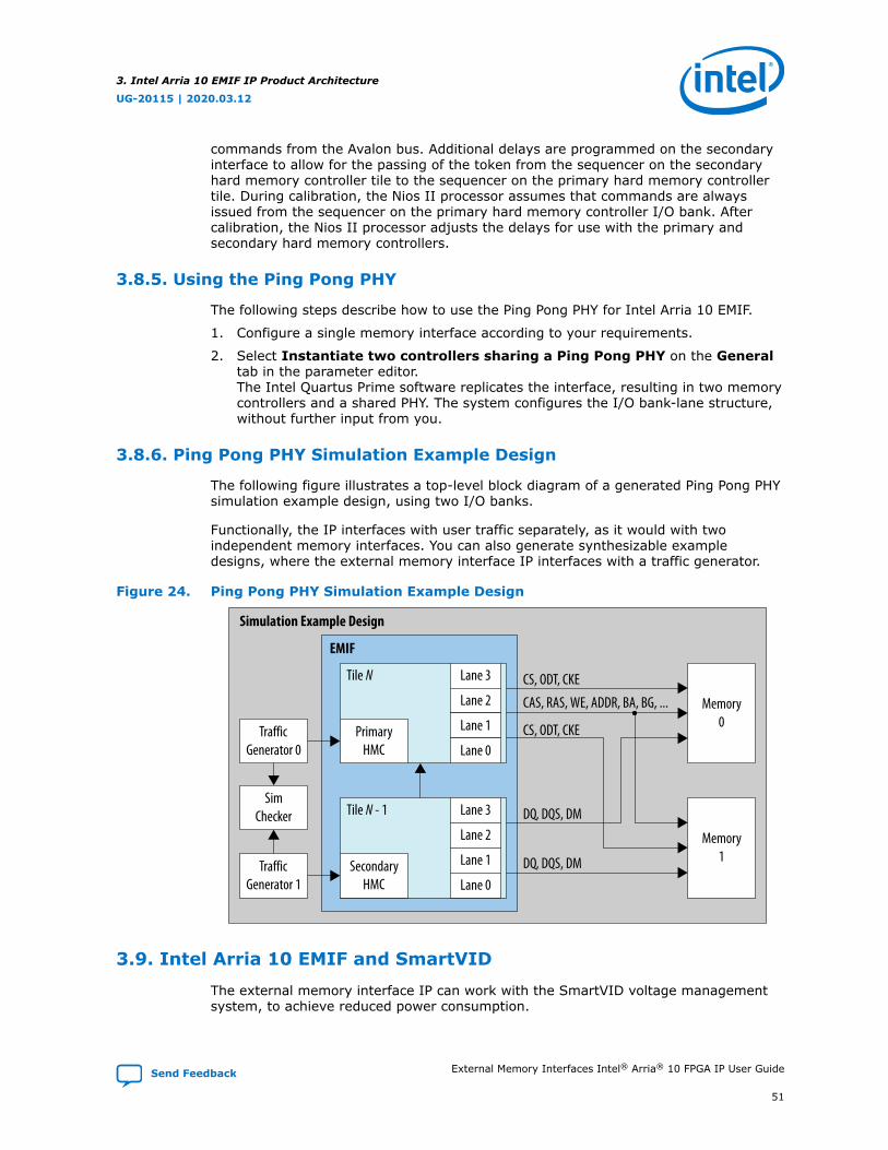
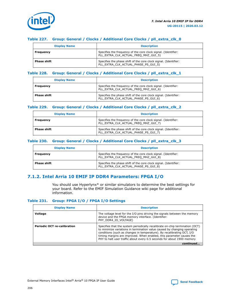
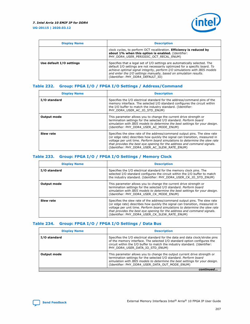
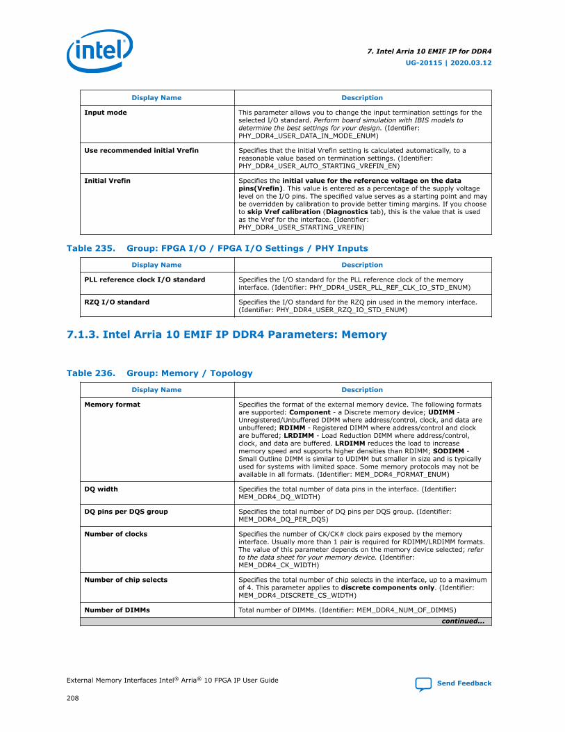
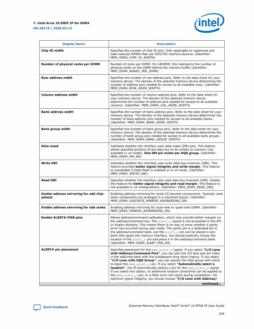
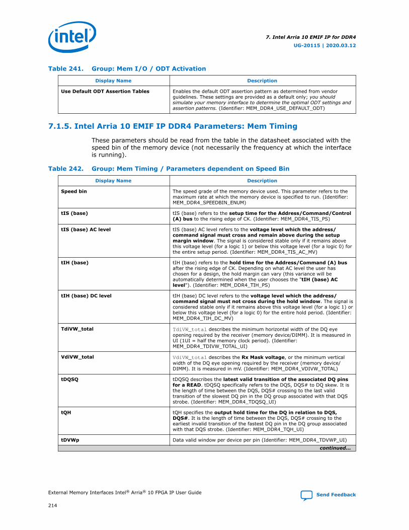
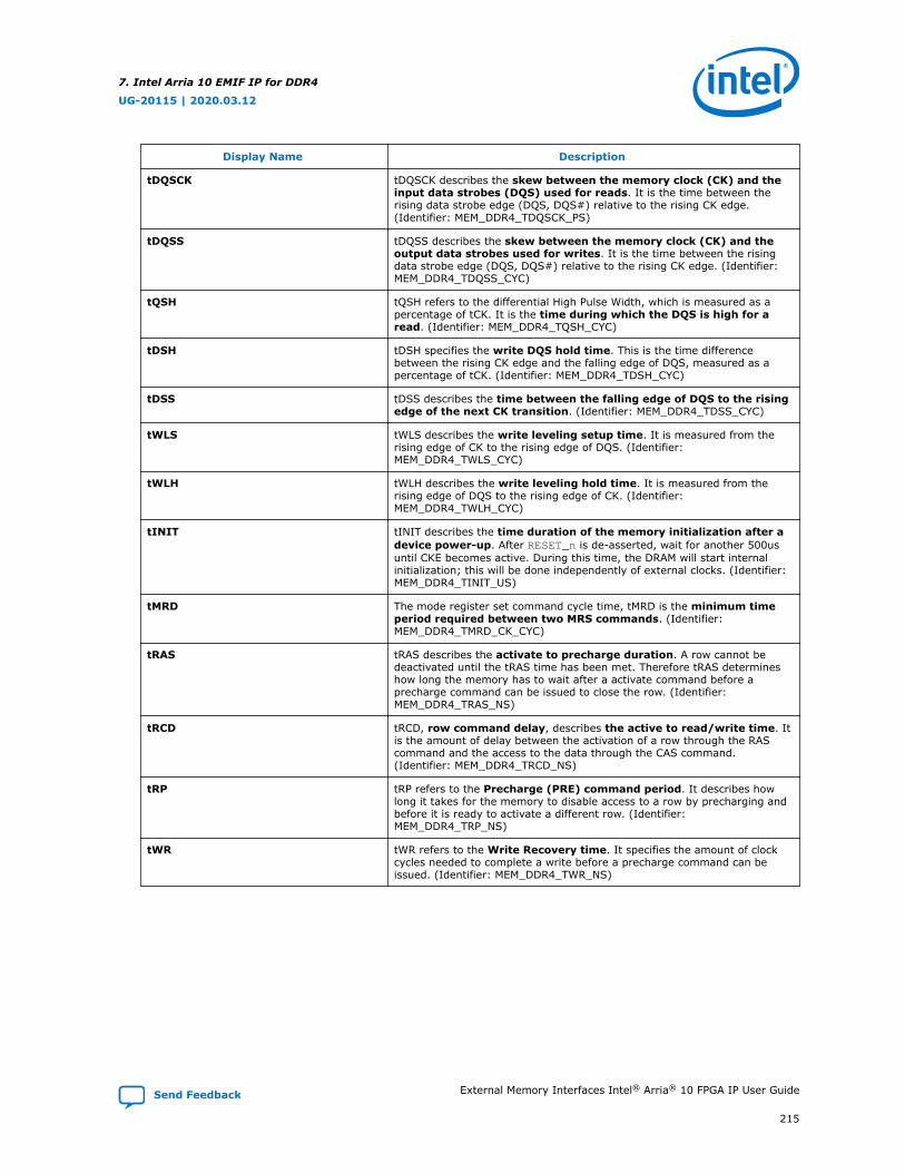
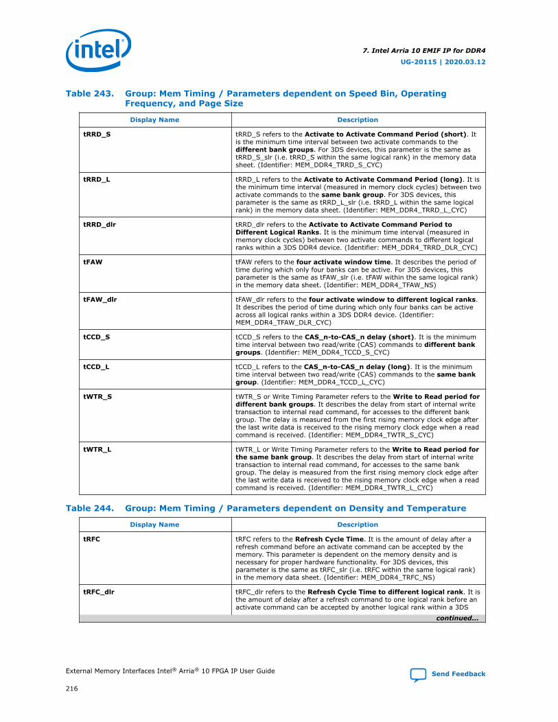
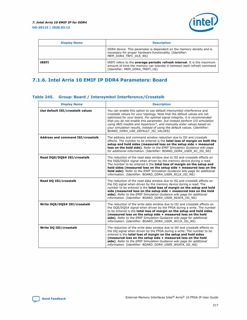
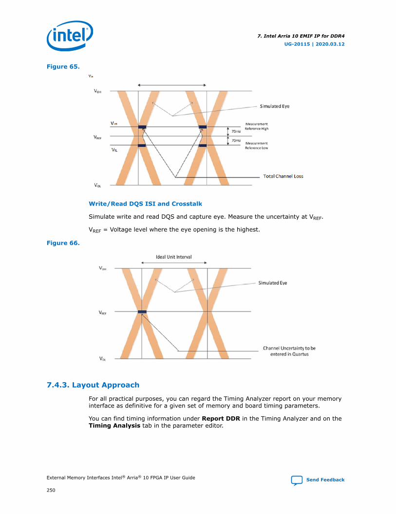
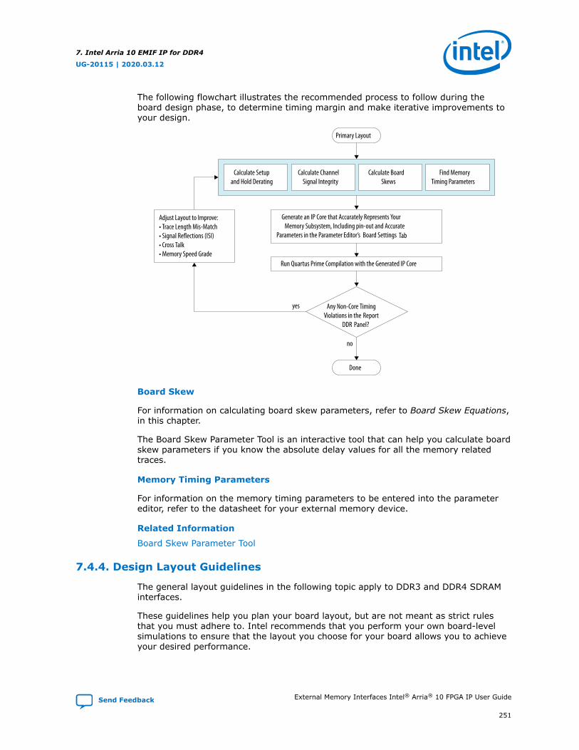
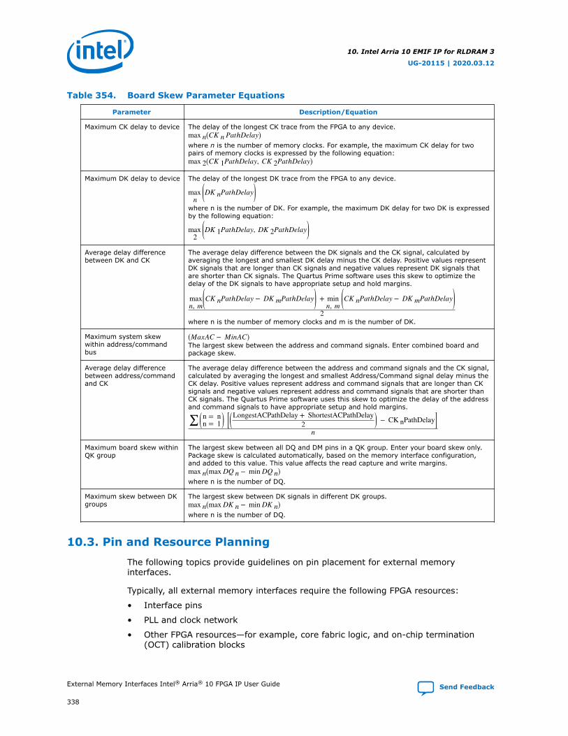
External Memory Interfaces Intel ® Arria ® 10 FPGA IP User Guide Updated for Intel ® Quartus ® Prime Design Suite: 19.3 IP Version: 19.1.0 Subscribe Send Feedback UG-20115 | 2020.03.12 Latest document on the web: PDF | HTML
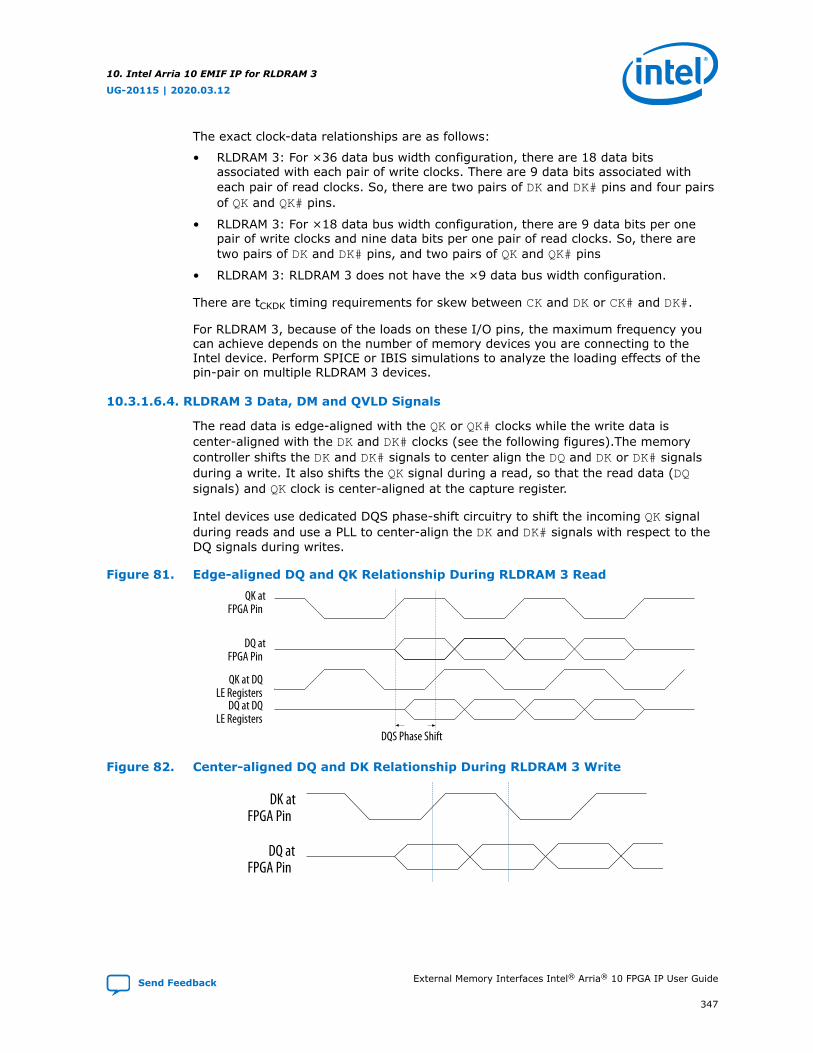
Transcript
External Memory Interfaces Intel®Arria® 10 FPGA IP User Guide
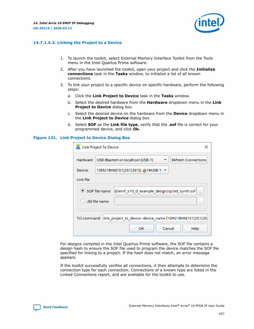
Updated for Intel® Quartus® Prime Design Suite: 19.3
IP Version: 19.1.0
SubscribeSend Feedback
UG-20115 | 2020.03.12Latest document on the web: PDF | HTML
3.5. Intel Arria 10 EMIF Controller................................................................................ 343.5.1. Hard Memory Controller............................................................................343.5.2. Hard Memory Controller Rate Conversion Feature.........................................38
3.6. Hardware Resource Sharing Among Multiple EMIFs...................................................393.6.1. I/O Aux Sharing.......................................................................................393.6.2. I/O Bank Sharing.....................................................................................393.6.3. PLL Reference Clock Sharing......................................................................413.6.4. Core Clock Network Sharing...................................................................... 42
3.7. Intel Arria 10 EMIF for Hard Processor Subsystem....................................................423.7.1. Restrictions on I/O Bank Usage for Intel Arria 10 EMIF IP with HPS.................433.7.2. Using the EMIF Debug Toolkit with Intel Arria 10 HPS Interfaces.....................45
4. Intel Arria 10 EMIF IP End-User Signals....................................................................... 534.1. Interface and Signal Descriptions........................................................................... 53
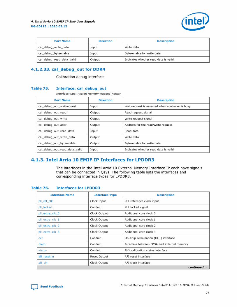
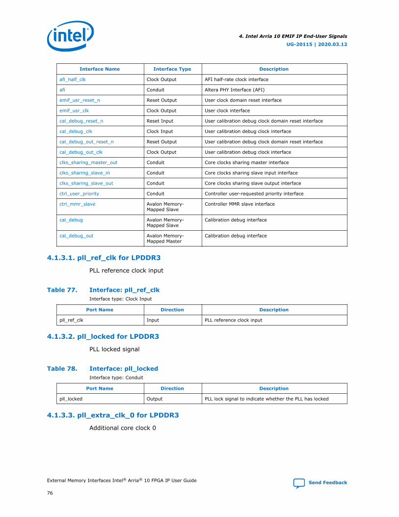
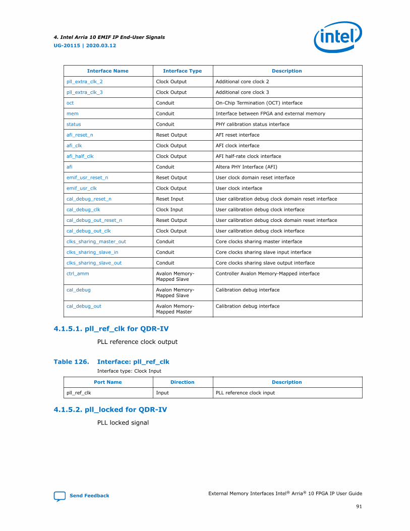
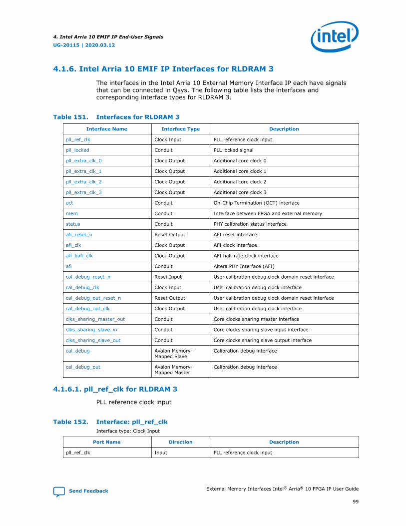
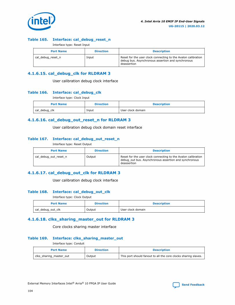
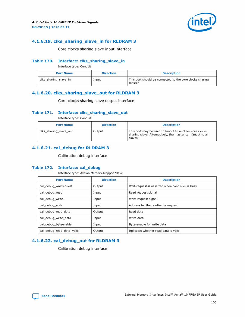
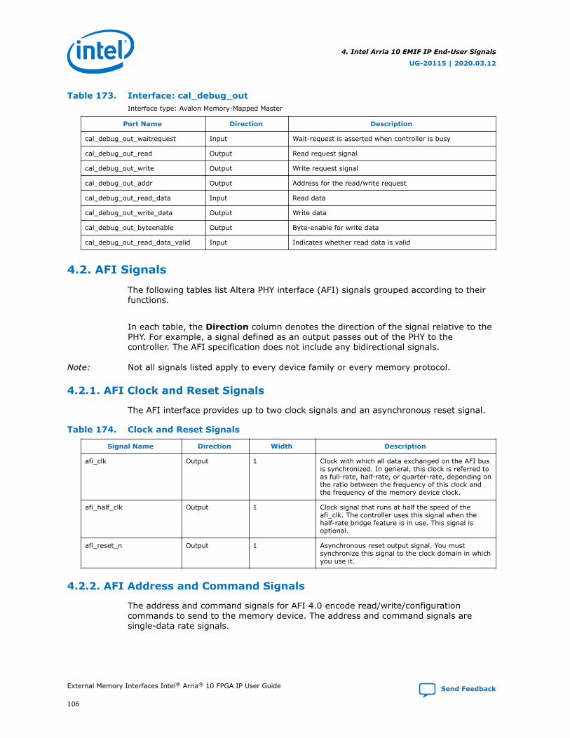
4.1.1. Intel Arria 10 EMIF IP Interfaces for DDR3.................................................. 534.1.2. Intel Arria 10 EMIF IP Interfaces for DDR4.................................................. 644.1.3. Intel Arria 10 EMIF IP Interfaces for LPDDR3............................................... 754.1.4. Intel Arria 10 EMIF IP Interfaces for QDR II/II+/II+ Xtreme.......................... 844.1.5. Intel Arria 10 EMIF IP Interfaces for QDR-IV................................................ 904.1.6. Intel Arria 10 EMIF IP Interfaces for RLDRAM 3............................................ 99
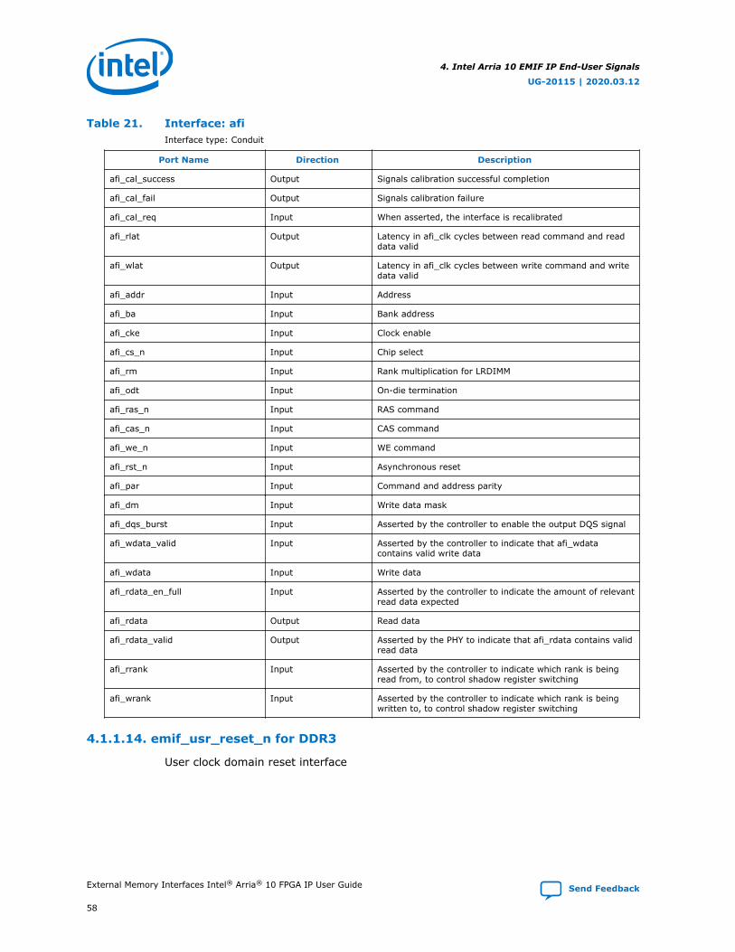
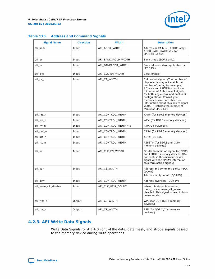
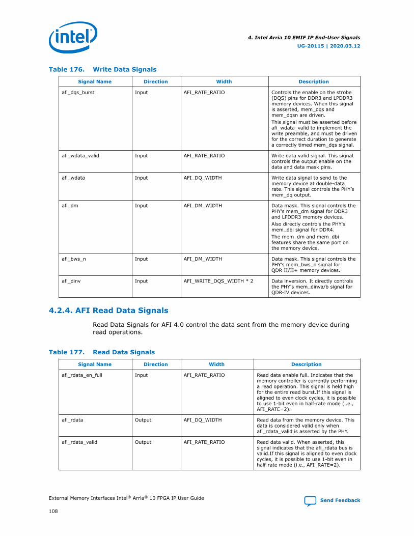
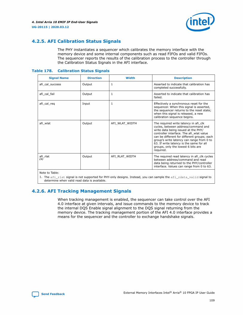
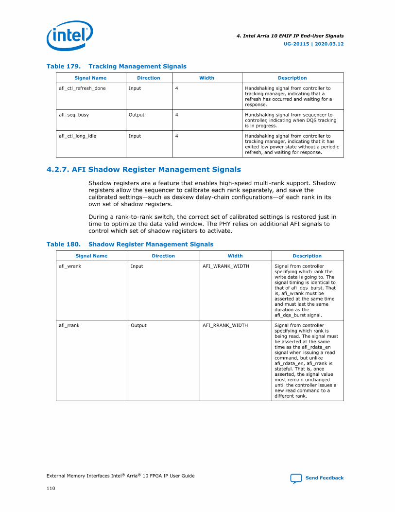
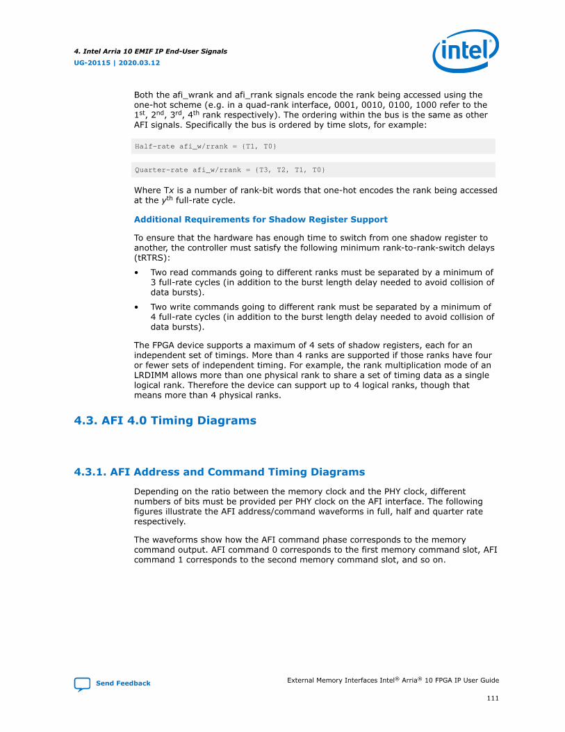
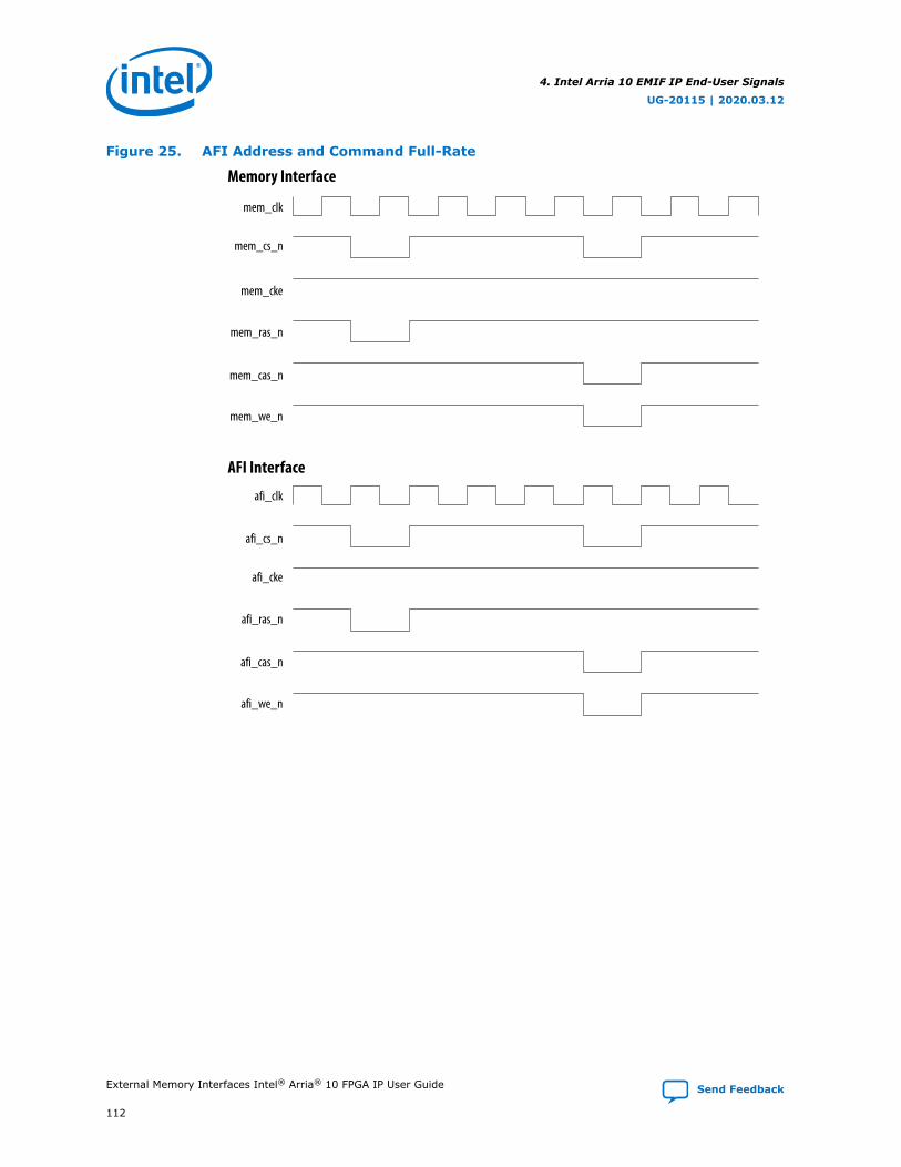
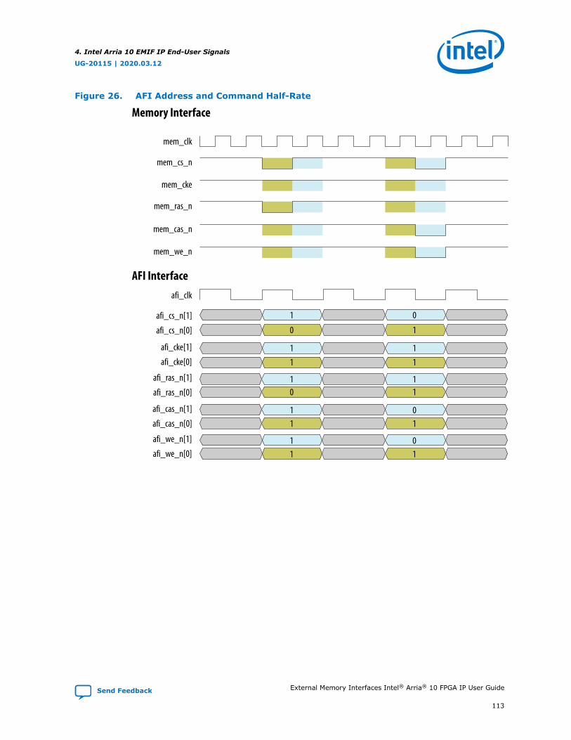
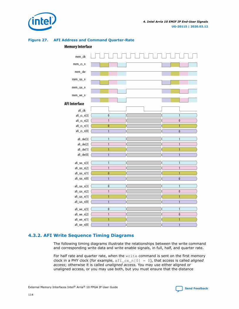
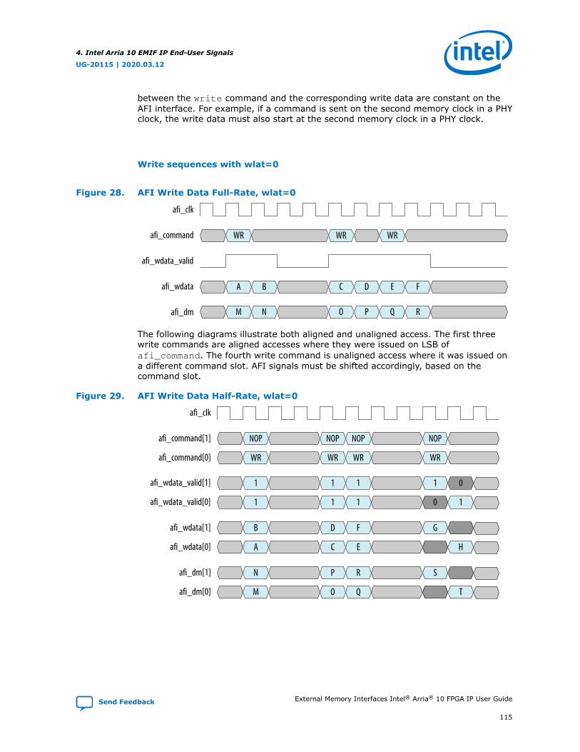
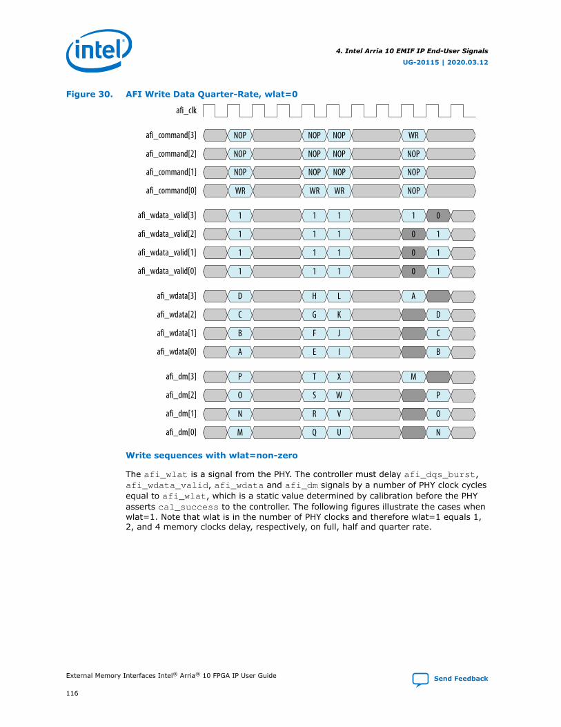
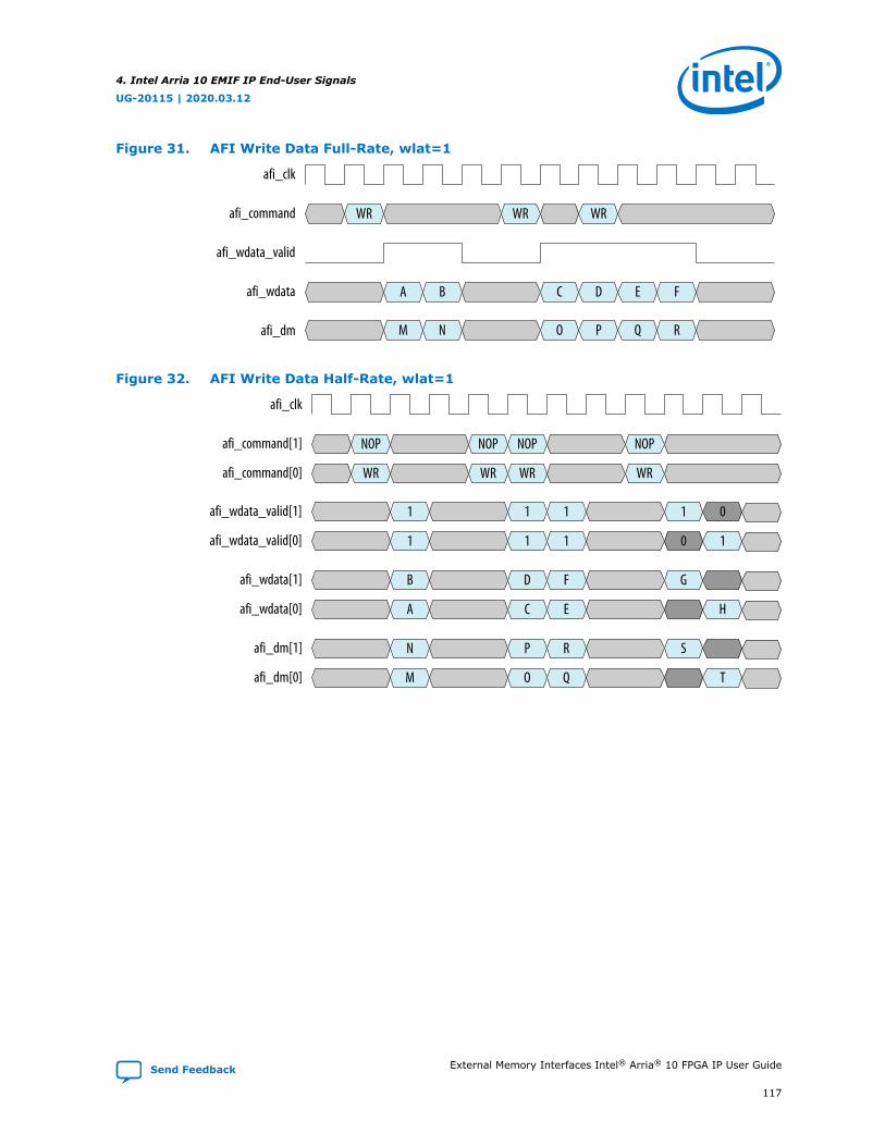
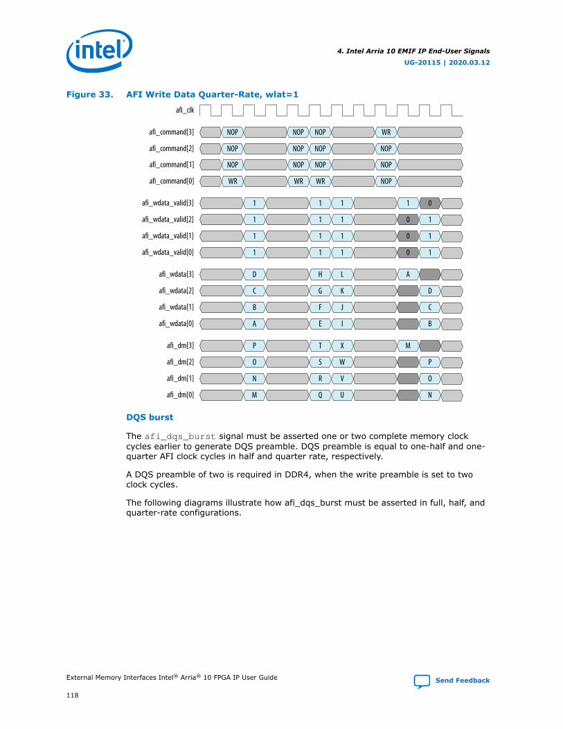
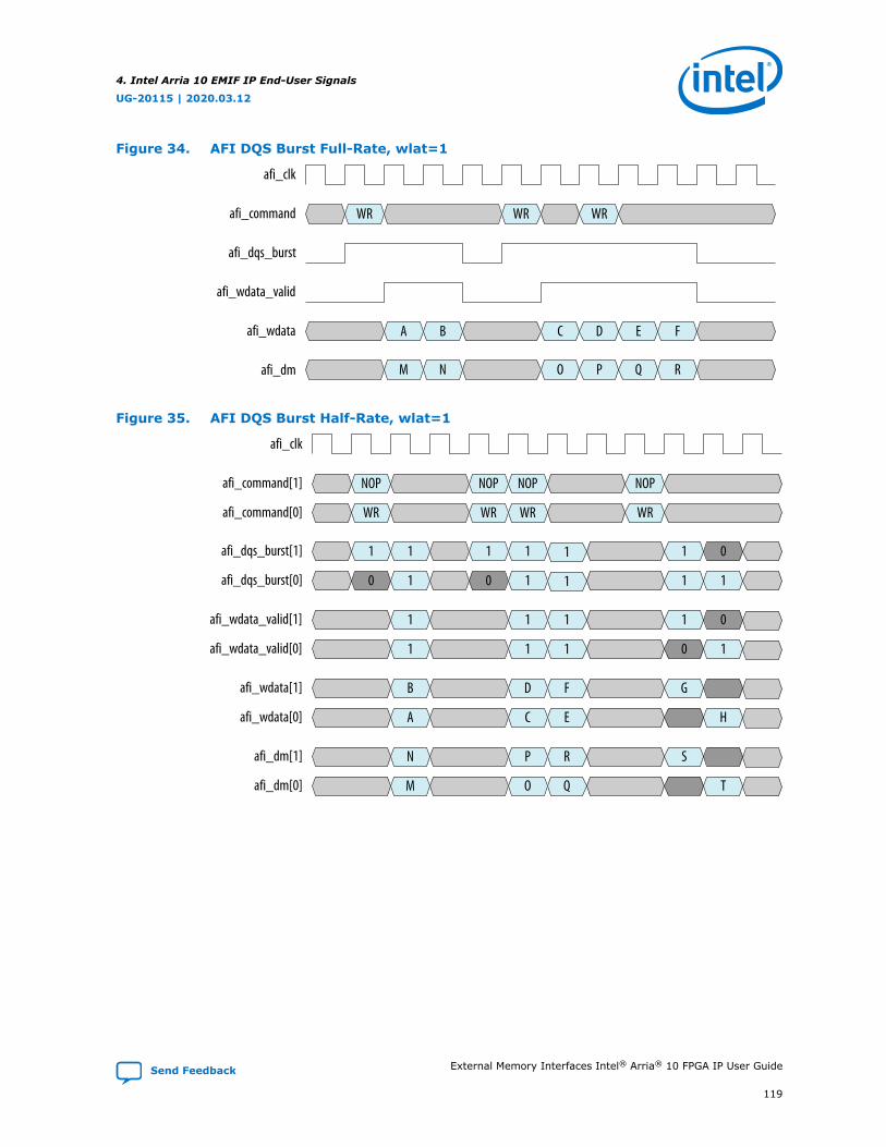
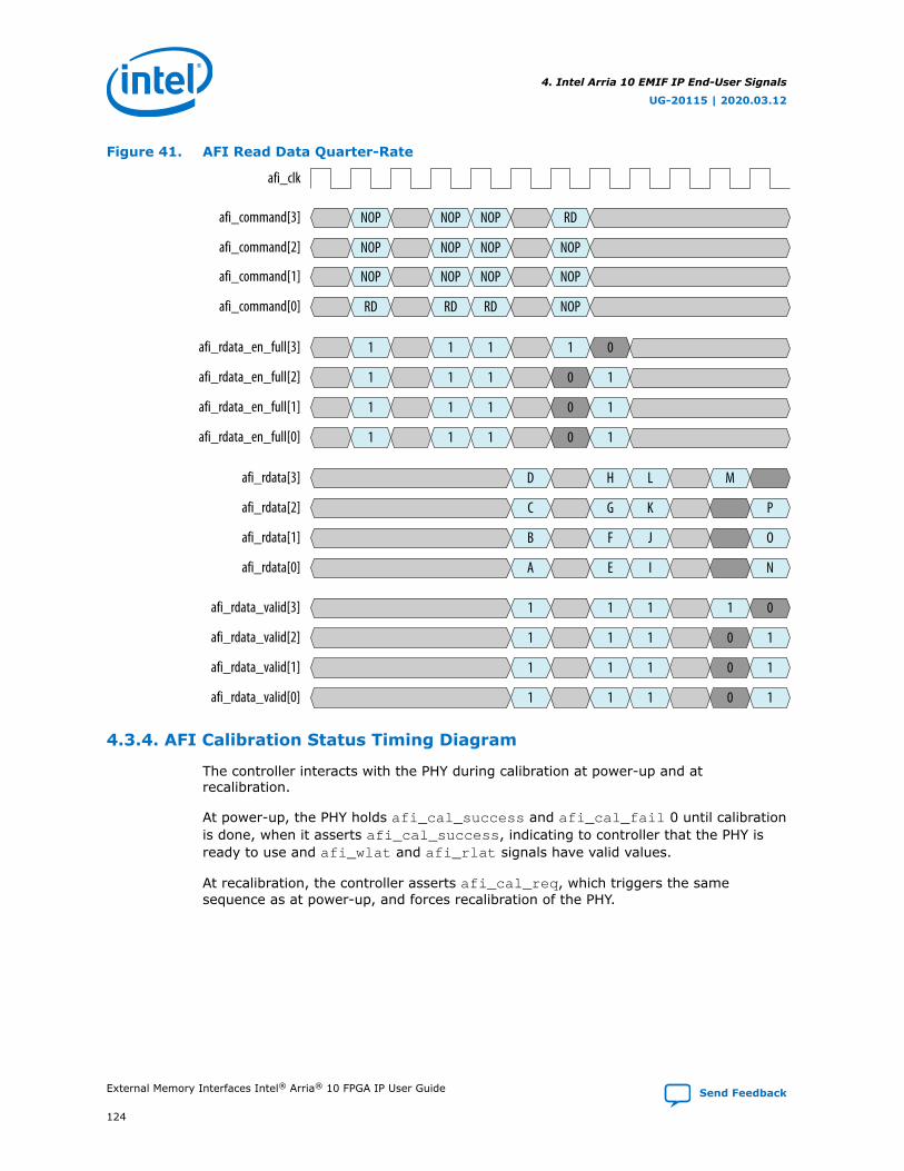
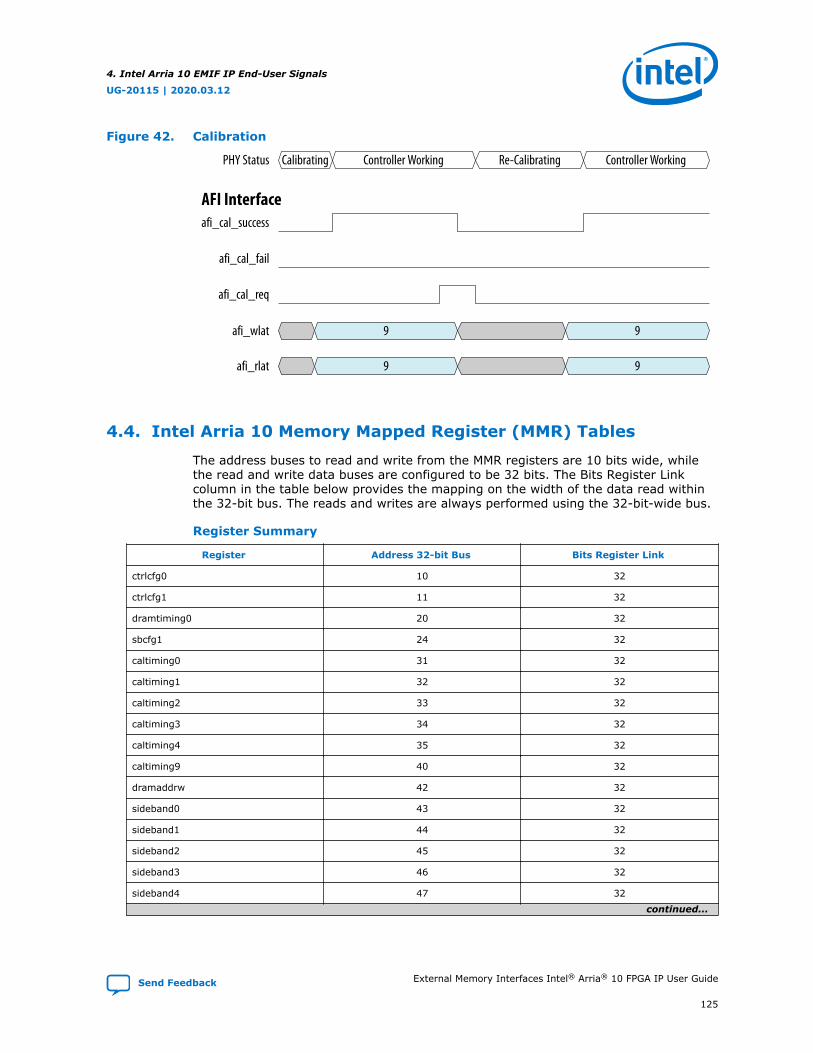
4.2. AFI Signals........................................................................................................1064.2.1. AFI Clock and Reset Signals.....................................................................1064.2.2. AFI Address and Command Signals...........................................................1064.2.3. AFI Write Data Signals............................................................................ 1074.2.4. AFI Read Data Signals............................................................................ 1084.2.5. AFI Calibration Status Signals.................................................................. 1094.2.6. AFI Tracking Management Signals............................................................ 1094.2.7. AFI Shadow Register Management Signals.................................................110
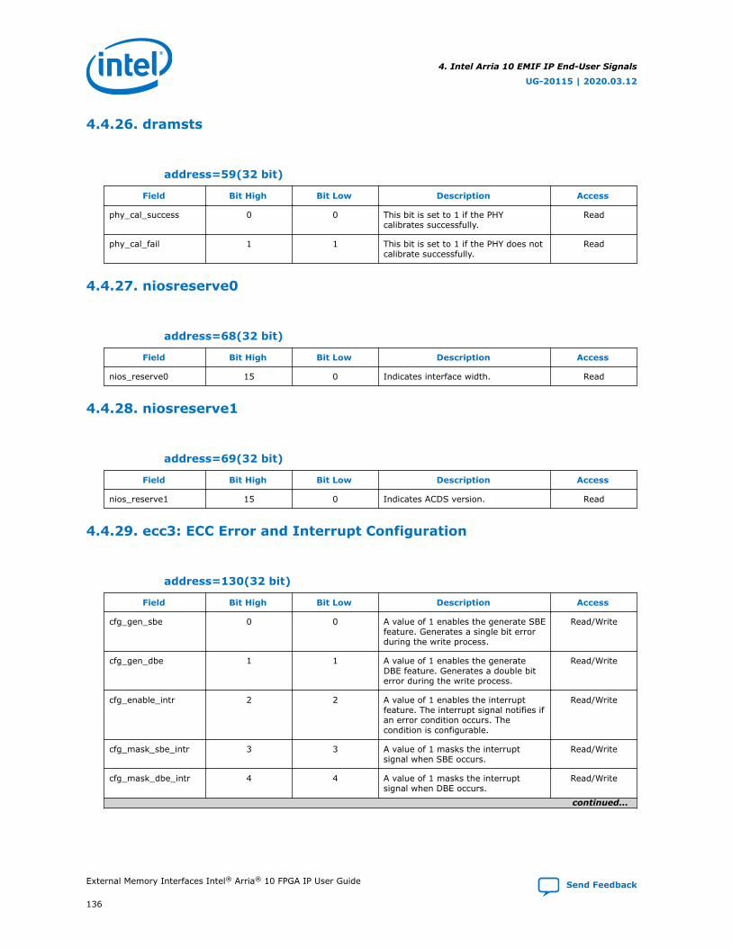
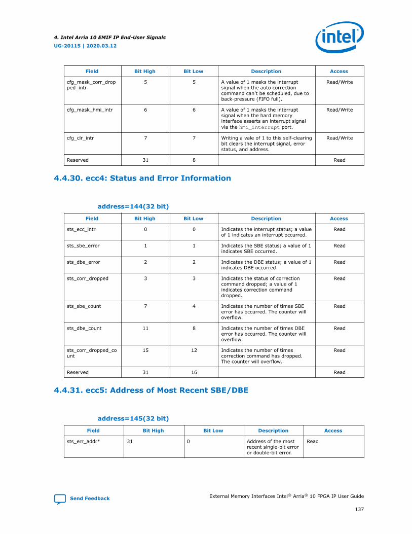
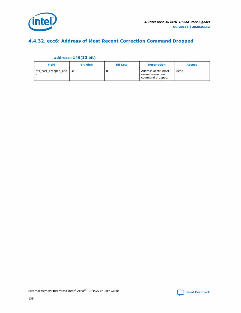
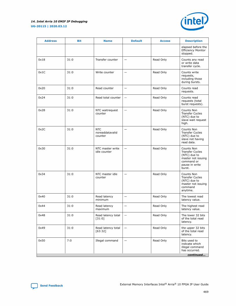
4.4.29. ecc3: ECC Error and Interrupt Configuration.............................................1364.4.30. ecc4: Status and Error Information.........................................................1374.4.31. ecc5: Address of Most Recent SBE/DBE................................................... 1374.4.32. ecc6: Address of Most Recent Correction Command Dropped......................138
12.4. Early I/O Timing Estimation............................................................................... 41312.4.1. Performing Early I/O Timing Analysis...................................................... 413
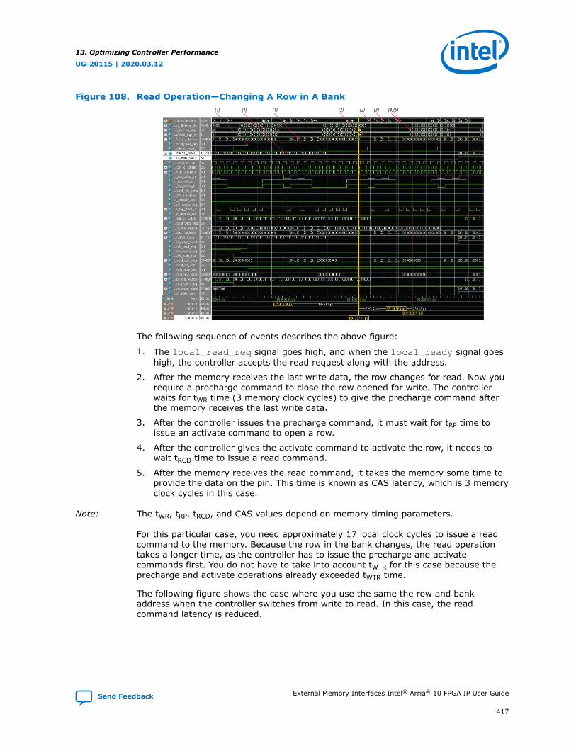
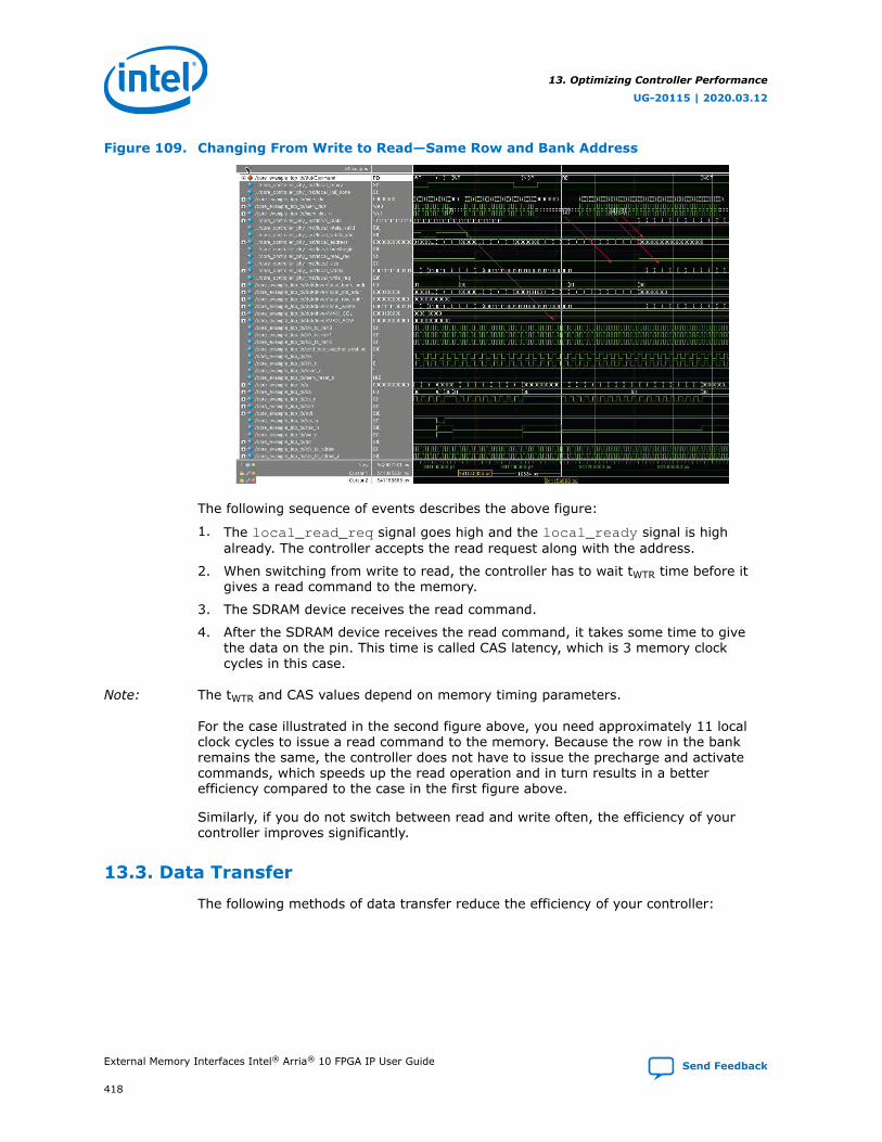
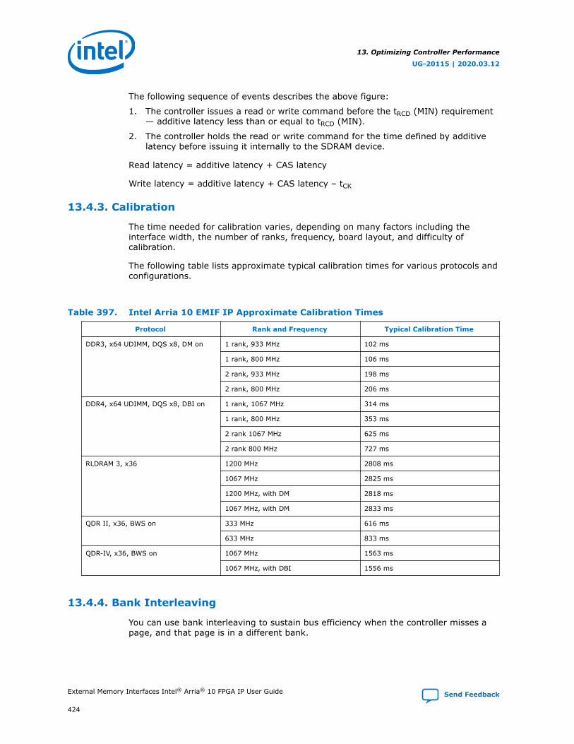
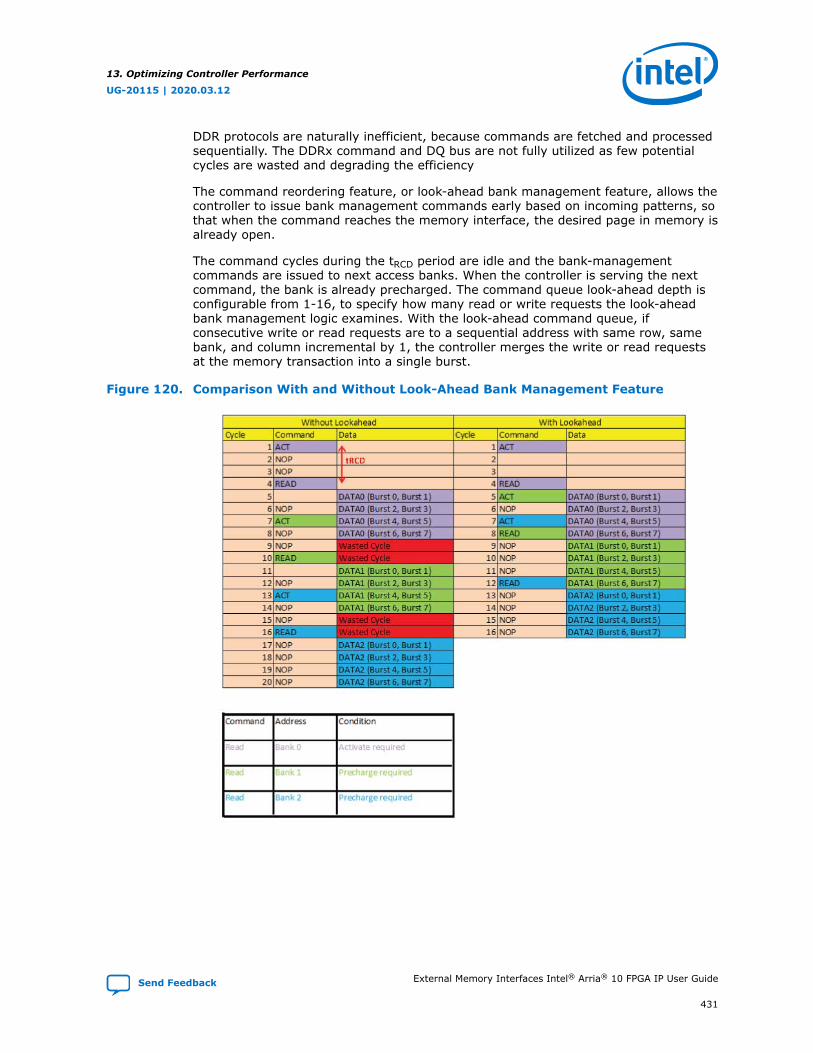
13. Optimizing Controller Performance........................................................................... 41513.1. Interface Standard........................................................................................... 41513.2. Bank Management Efficiency..............................................................................41613.3. Data Transfer...................................................................................................41813.4. Improving Controller Efficiency...........................................................................419
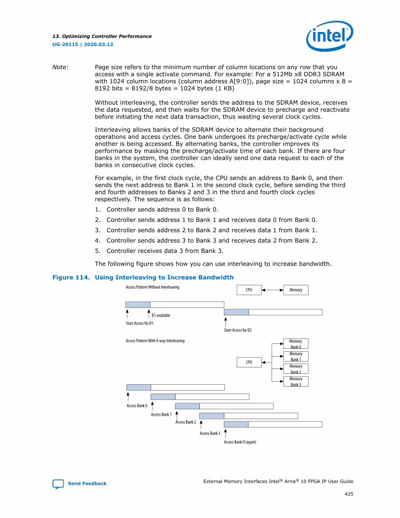
13.4.1. Auto-Precharge Commands....................................................................42013.4.2. Latency...............................................................................................42213.4.3. Calibration...........................................................................................42413.4.4. Bank Interleaving................................................................................. 42413.4.5. Additive Latency and Bank Interleaving................................................... 42613.4.6. User-Controlled Refresh........................................................................ 42713.4.7. Frequency of Operation......................................................................... 42913.4.8. Series of Reads or Writes.......................................................................42913.4.9. Data Reordering...................................................................................42913.4.10. Starvation Control...............................................................................43013.4.11. Command Reordering..........................................................................43013.4.12. Bandwidth......................................................................................... 43213.4.13. Enable Command Priority Control..........................................................432
14.2.1. Intel IP Memory Model.......................................................................... 43614.2.2. Vendor Memory Model...........................................................................43614.2.3. Transcript Window Messages..................................................................43614.2.4. Modifying the Example Driver to Replicate the Failure................................438
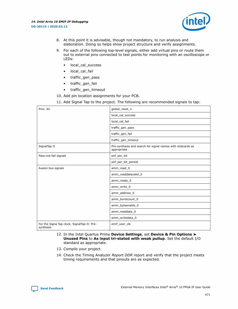
14.4. Verifying Memory IP Using the Signal Tap II Logic Analyzer.................................... 44114.4.1. Signals to Monitor with the Signal Tap II Logic Analyzer.............................442
14.5. Hardware Debugging Guidelines......................................................................... 44314.5.1. Create a Simplified Design that Demonstrates the Same Issue................... 44314.5.2. Measure Power Distribution Network....................................................... 44414.5.3. Measure Signal Integrity and Setup and Hold Margin.................................44414.5.4. Vary Voltage........................................................................................ 44414.5.5. Operate at a Lower Speed..................................................................... 44414.5.6. Determine Whether the Issue Exists in Previous Versions of Software.......... 44414.5.7. Determine Whether the Issue Exists in the Current Version of Software....... 44514.5.8. Try A Different PCB...............................................................................44514.5.9. Try Other Configurations........................................................................44614.5.10. Debugging Checklist............................................................................446
14.6. Categorizing Hardware Issues............................................................................ 44714.6.1. Signal Integrity Issues.......................................................................... 44714.6.2. Hardware and Calibration Issues.............................................................449
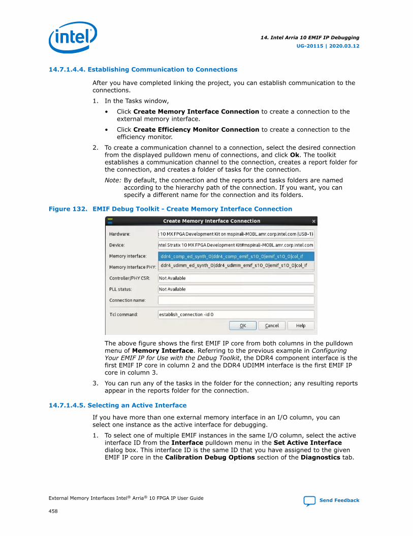
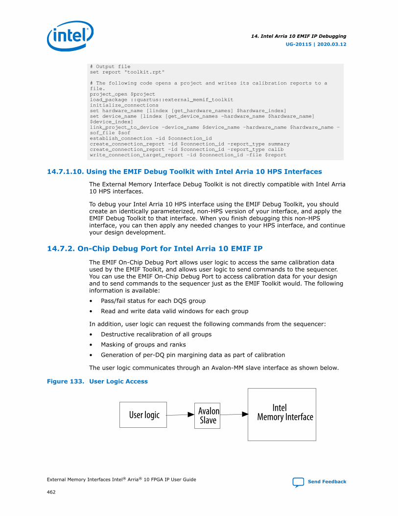
14.7.2. On-Chip Debug Port for Intel Arria 10 EMIF IP.......................................... 46214.7.3. Efficiency Monitor and Protocol Checker...................................................464
14.8. Using the Traffic Generator with the Generated Design Example..............................470
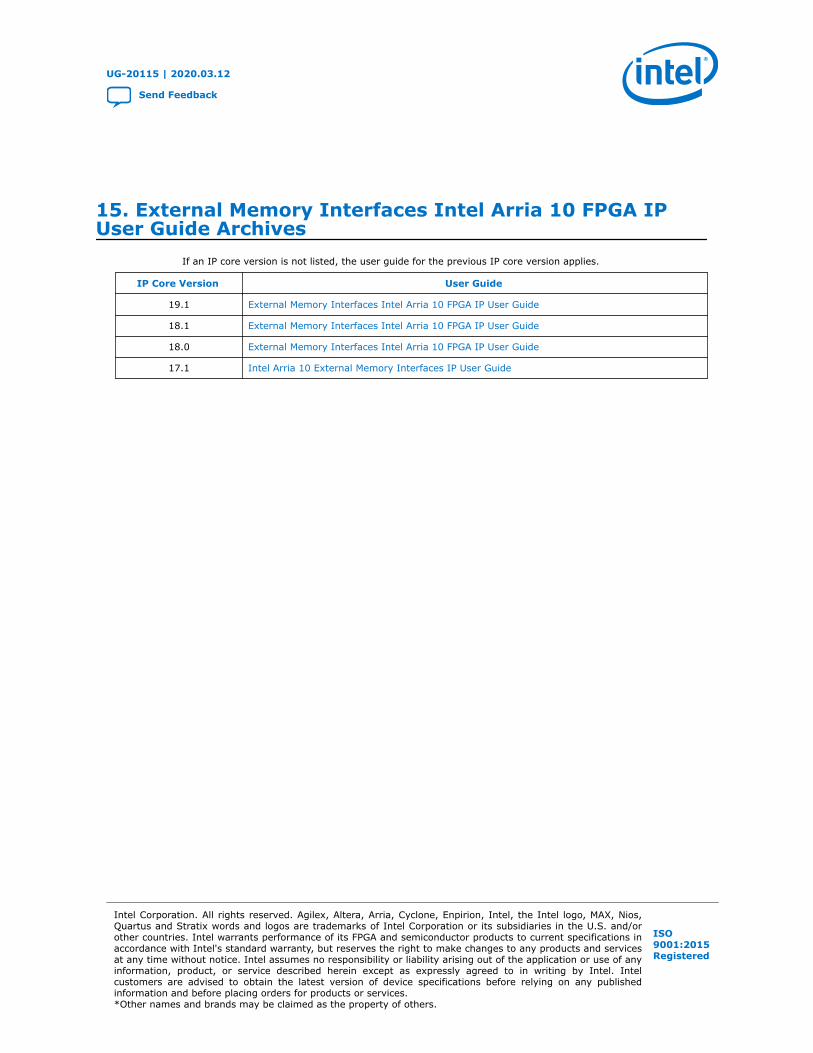
15. External Memory Interfaces Intel Arria 10 FPGA IP User Guide Archives..................473
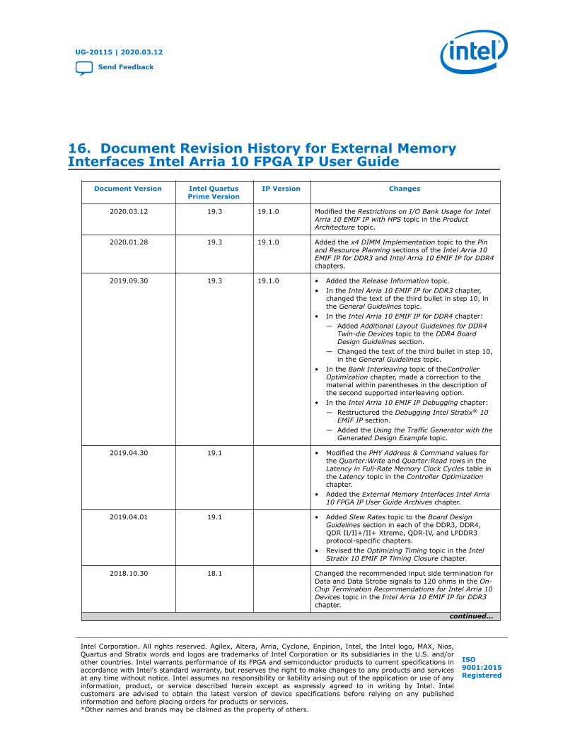
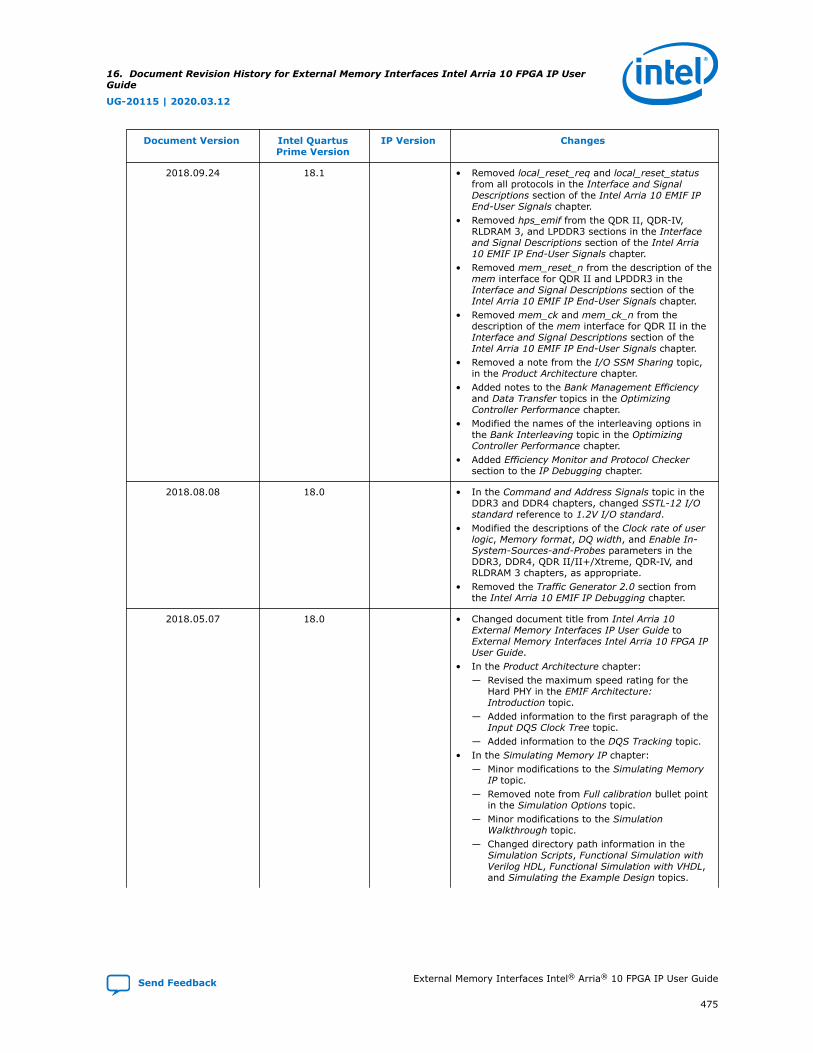
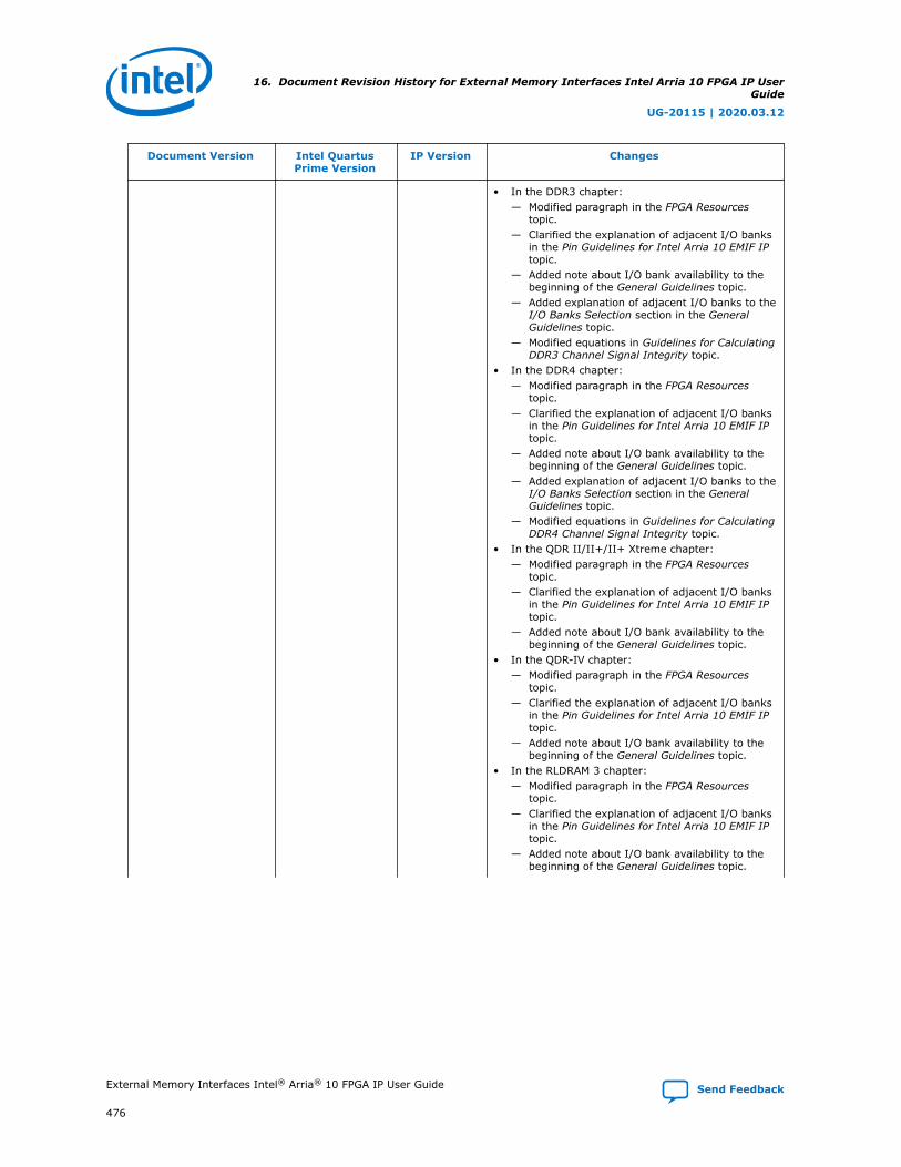
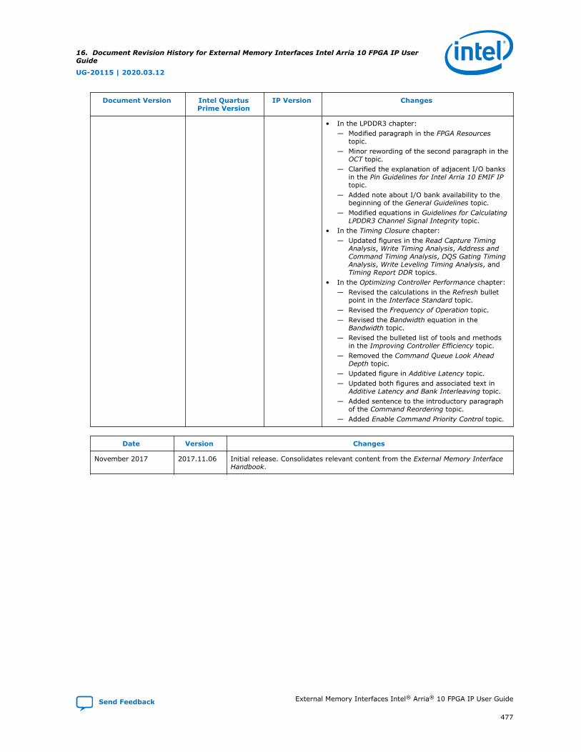
16. Document Revision History for External Memory Interfaces Intel Arria 10 FPGAIP User Guide........................................................................................................ 474
Contents
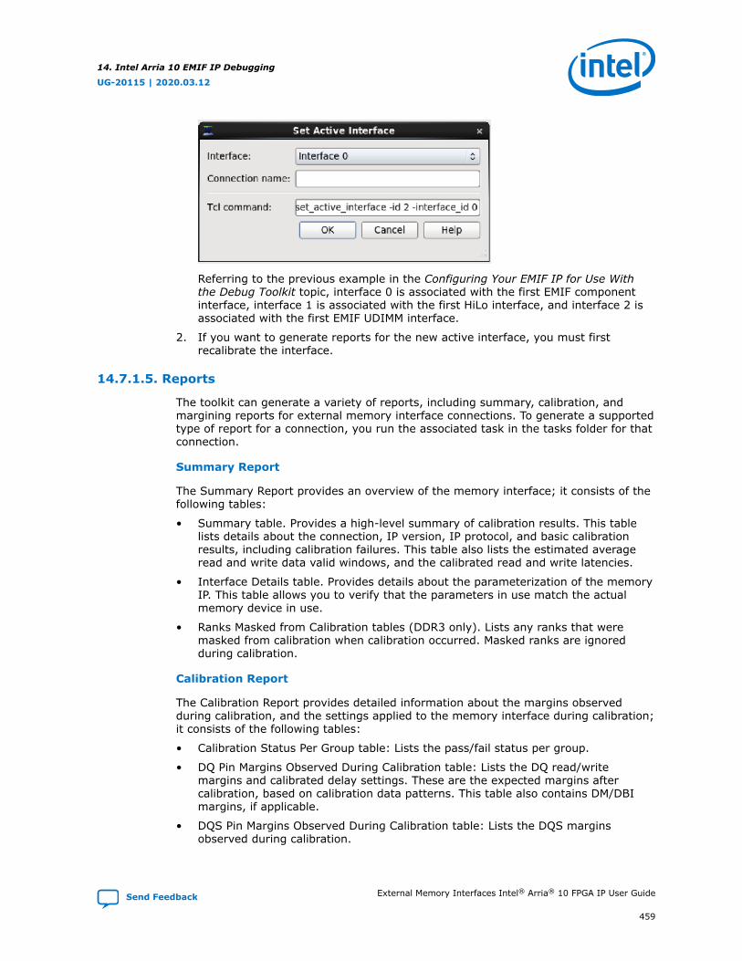
External Memory Interfaces Intel® Arria® 10 FPGA IP User Guide Send Feedback
IP versions are the same as the Intel® Quartus® Prime Design Suite software versionsup to v19.1. From Intel Quartus Prime Design Suite software version 19.2 or later, IPcores have a new IP versioning scheme.
The IP versioning scheme (X.Y.Z) number changes from one software version toanother. A change in:
• X indicates a major revision of the IP. If you update your Intel Quartus Primesoftware, you must regenerate the IP.
• Y indicates the IP includes new features. Regenerate your IP to include these newfeatures.
• Z indicates the IP includes minor changes. Regenerate your IP to include thesechanges.
Table 1.
Item Description
IP Version 19.1.0
Intel Quartus Prime 19.3
Release Date 2019.09.30
UG-20115 | 2020.03.12
Send Feedback
Intel Corporation. All rights reserved. Agilex, Altera, Arria, Cyclone, Enpirion, Intel, the Intel logo, MAX, Nios,Quartus and Stratix words and logos are trademarks of Intel Corporation or its subsidiaries in the U.S. and/orother countries. Intel warrants performance of its FPGA and semiconductor products to current specifications inaccordance with Intel's standard warranty, but reserves the right to make changes to any products and servicesat any time without notice. Intel assumes no responsibility or liability arising out of the application or use of anyinformation, product, or service described herein except as expressly agreed to in writing by Intel. Intelcustomers are advised to obtain the latest version of device specifications before relying on any publishedinformation and before placing orders for products or services.*Other names and brands may be claimed as the property of others.
Intel's fast, efficient, and low-latency external memory interface (EMIF) intellectualproperty (IP) cores easily interface with today's higher speed memory devices.
You can easily implement the EMIF IP core functions through the Intel Quartus Primesoftware. The Intel Quartus Prime software also provides external memory toolkitsthat help you test the implementation of the IP in the FPGA.
The External Memory Interfaces Intel Arria® 10 FPGA IP (referred to hereafter as theIntel Arria 10 EMIF IP) provides the following components:
• A physical layer interface (PHY) which builds the data path and manages timingtransfers between the FPGA and the memory device.
• A memory controller which implements all the memory commands and protocol-level requirements.
For information on the maximum speeds supported by the external memory interfaceIP, refer to the External Memory Interface Spec Estimator.
Intel Arria 10 Protocol and Feature Support
• Supports DDR4, DDR3, and LPDDR3 protocols with hard memory controller andhard PHY.
• Supports QDR-IV, QDR II + Xtreme, QDR II +, and QDR II using soft memorycontroller and hard PHY.
• Supports RLDRAM 3 using third-party soft controller.
• Supports Ping Pong PHY mode, allowing two memory controllers to sharecommand, address, and control pins.
• Supports error correction code (ECC) for both hard memory controller and softmemory controller.
Related Information
• Intel FPGA IP for External Memory Interfaces - Support Center
• Intel Arria 10 Core Fabric and General Purpose I/Os Handbook
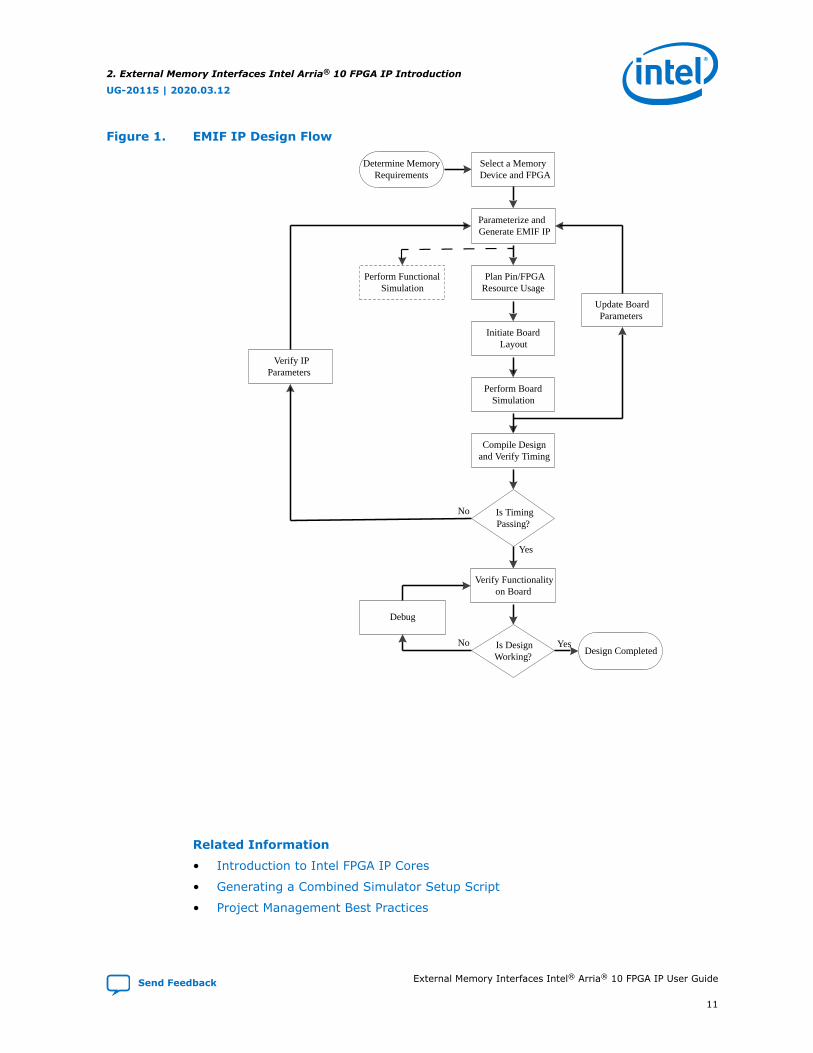
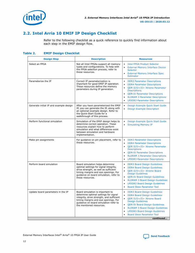
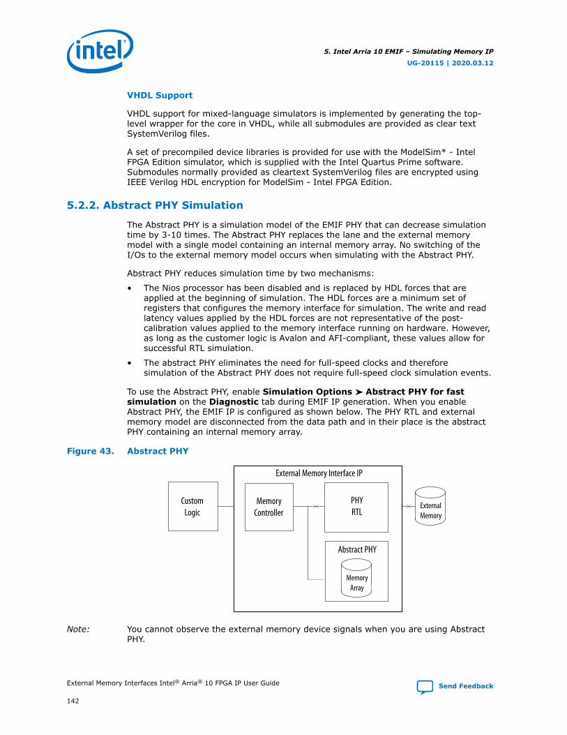
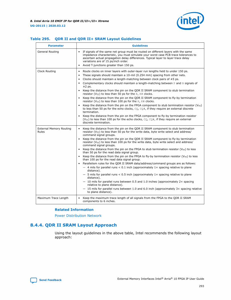
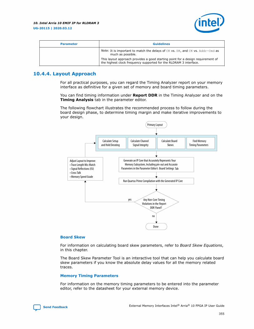
2.1. Intel Arria 10 EMIF IP Design Flow
Intel recommends creating an example top-level file with the desired pin outs and allinterface IPs instantiated. This enables the Intel Quartus Prime software to validatethe design and resource allocation before PCB and schematic sign off.
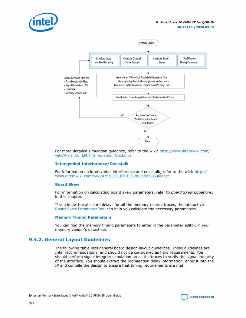
The following figure shows the design flow to provide the fastest out-of-the-boxexperience with the EMIF IP.
UG-20115 | 2020.03.12
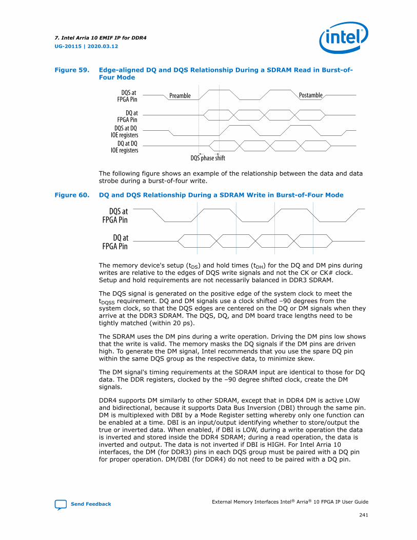
Send Feedback
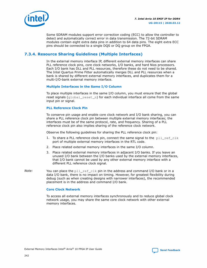
Intel Corporation. All rights reserved. Agilex, Altera, Arria, Cyclone, Enpirion, Intel, the Intel logo, MAX, Nios,Quartus and Stratix words and logos are trademarks of Intel Corporation or its subsidiaries in the U.S. and/orother countries. Intel warrants performance of its FPGA and semiconductor products to current specifications inaccordance with Intel's standard warranty, but reserves the right to make changes to any products and servicesat any time without notice. Intel assumes no responsibility or liability arising out of the application or use of anyinformation, product, or service described herein except as expressly agreed to in writing by Intel. Intelcustomers are advised to obtain the latest version of device specifications before relying on any publishedinformation and before placing orders for products or services.*Other names and brands may be claimed as the property of others.
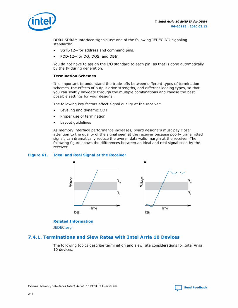
Parameterize the IP Correct IP parameterization isimportant for good EMIF IP operation.These resources define the memoryparameters during IP generation.
Generate initial IP and example design After you have parameterized the EMIFIP, you can generate the IP, along withan optional example design. Refer tothe Quick-Start Guide for awalkthrough of this process.
• Design Example Quick Start Guide• Design Example Description
Perform functional simulation Simulation of the EMIF design helps todetermine correct operation. Theseresources explain how to performsimulation and what differences existbetween simulation and hardwareimplementation.
• Design Example Quick Start Guide• Simulating Memory IP
Make pin assignments For guidance on pin placement, refer tothese resources.
Perform board simulation Board simulation helps determineoptimal settings for signal integrity,drive strength, as well as sufficienttiming margins and eye openings. Forguidance on board simulation, refer tothese resources.
Update board parameters in the IP Board simulation is important todetermine optimal settings for signalintegrity, drive strength, and sufficienttiming margins and eye openings. Forguidance on board simulation refer tothe mentioned resources.
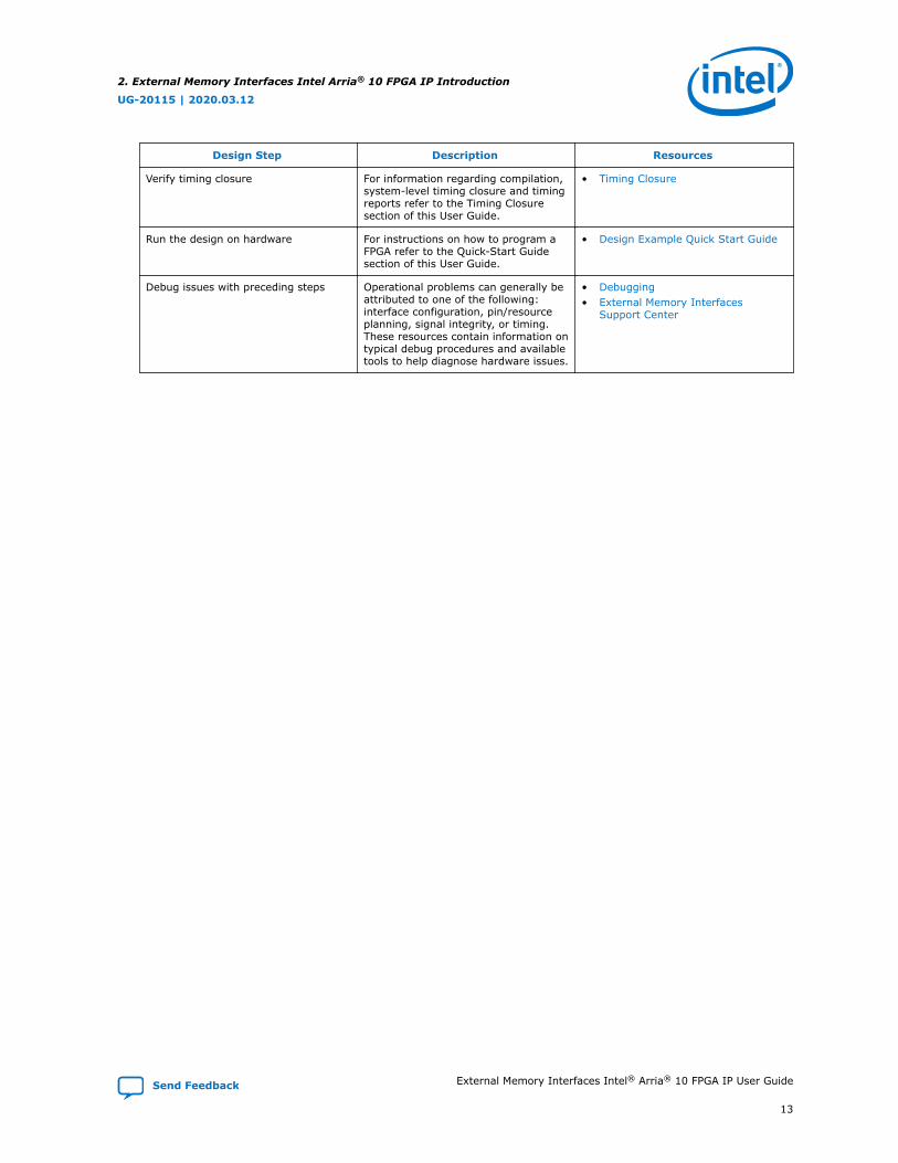
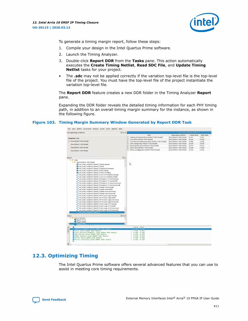
Verify timing closure For information regarding compilation,system-level timing closure and timingreports refer to the Timing Closuresection of this User Guide.
• Timing Closure
Run the design on hardware For instructions on how to program aFPGA refer to the Quick-Start Guidesection of this User Guide.
• Design Example Quick Start Guide
Debug issues with preceding steps Operational problems can generally beattributed to one of the following:interface configuration, pin/resourceplanning, signal integrity, or timing.These resources contain information ontypical debug procedures and availabletools to help diagnose hardware issues.
• Debugging• External Memory Interfaces
Support Center
2. External Memory Interfaces Intel Arria® 10 FPGA IP Introduction
UG-20115 | 2020.03.12
Send Feedback External Memory Interfaces Intel® Arria® 10 FPGA IP User Guide
3. Intel Arria 10 EMIF IP Product ArchitectureThis chapter describes the Intel Arria 10 product architecture.
3.1. EMIF Architecture: Introduction
The Intel Arria 10 architecture contains many hardware features designed to meet thehigh-speed requirements of emerging memory protocols, while consuming thesmallest amount of core logic area and power.
The following are key hardware features of the architecture:
Hard Sequencer
The sequencer employs a hard Nios II processor, and can perform memory calibrationfor a wide range of protocols. You can share the sequencer among multiple memoryinterfaces of the same or different protocols.
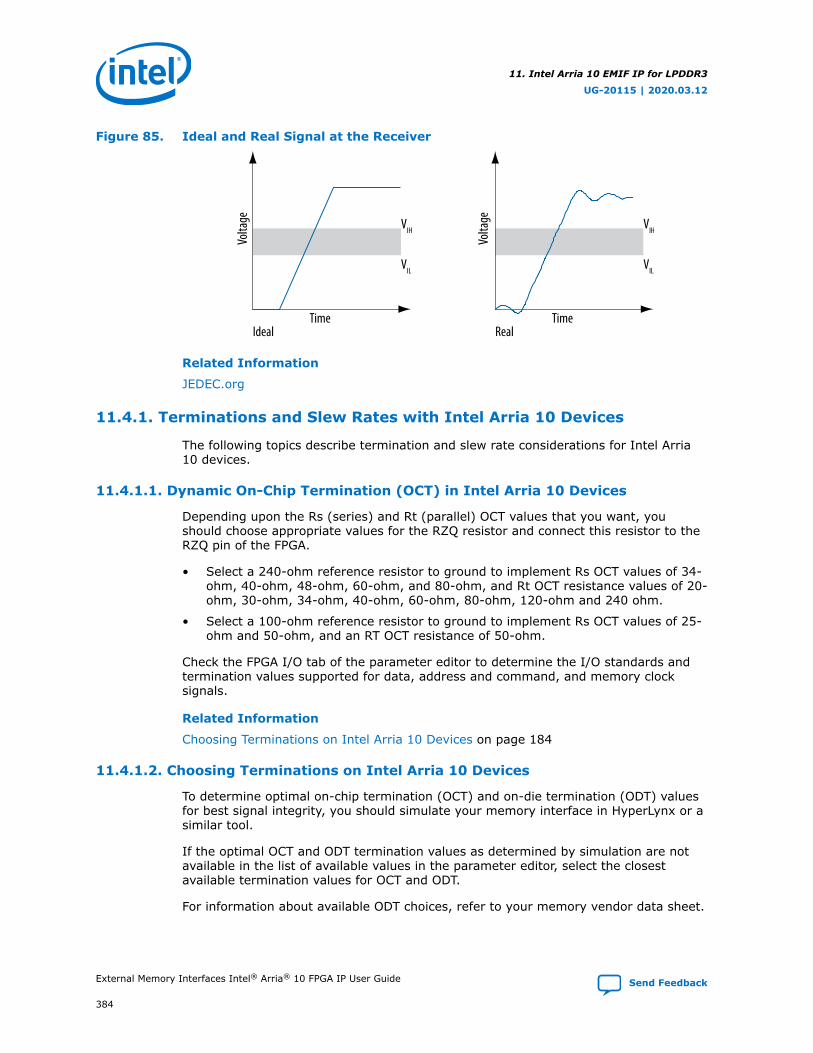
Hard PHY
The hard PHY can interface with external memories running at speeds of up to 1.2GHz. The PHY circuitry is hardened in the silicon, which simplifies the challenges ofachieving timing closure and minimal power consumption.
Hard Memory Controller
The hard memory controller reduces latency and minimizes core logic consumption inthe external memory interface. The hard memory controller supports the DDR3,DDR4, and LPDDR3 memory protocols.
PHY-Only Mode
The EMIF IP provides a PHY-only option, which allows you to use your own custom softcontroller. When selected, the PHY-only option generates only the PHY and sequencer,but not the controller, thus providing a mechanism by which you can integrate yourown custom soft controller.
High-Speed PHY Clock Tree
Dedicated high speed PHY clock networks clock the I/O buffers. The PHY clock treesexhibit low jitter and low duty cycle distortion, maximizing the data valid window.
Automatic Clock Phase Alignment
Automatic clock phase alignment circuitry dynamically adjusts the clock phase of coreclock networks to match the clock phase of the PHY clock networks. The clock phasealignment circuitry minimizes clock skew that can complicate timing closure intransfers between the FPGA core and the periphery.
UG-20115 | 2020.03.12
Send Feedback
Intel Corporation. All rights reserved. Agilex, Altera, Arria, Cyclone, Enpirion, Intel, the Intel logo, MAX, Nios,Quartus and Stratix words and logos are trademarks of Intel Corporation or its subsidiaries in the U.S. and/orother countries. Intel warrants performance of its FPGA and semiconductor products to current specifications inaccordance with Intel's standard warranty, but reserves the right to make changes to any products and servicesat any time without notice. Intel assumes no responsibility or liability arising out of the application or use of anyinformation, product, or service described herein except as expressly agreed to in writing by Intel. Intelcustomers are advised to obtain the latest version of device specifications before relying on any publishedinformation and before placing orders for products or services.*Other names and brands may be claimed as the property of others.
The device architecture simplifies resource sharing between memory interfaces.Resources such as the OCT calibration block, PLL reference clock pin, and core clockcan be shared. The hard Nios processor in the I/O AUX is shared across all interfacesin a column.
3.1.1. I/O Subsystem
The I/O subsystem consists of two columns inside the core of the Intel Arria 10device.
Each column can be thought of as loosely analogous to an I/O bank.
Figure 2. I/O Subsystem
Core FabricI/O ColumnTransceivers (if applicable)
The I/O subsystem provides the following features:
• General-purpose I/O registers and I/O buffers
• On-chip termination control (OCT)
• I/O PLLs for external memory interfaces and user logic
• Low-voltage differential signaling (LVDS)
• External memory interface components, as follows:
— Hard memory controller
— Hard PHY
— Hard Nios processor and calibration logic
— DLL
3.1.2. I/O Column
Intel Arria 10 devices have two I/O columns which contain the hardware related toexternal memory interfaces.
Each I/O column contains the following major parts:
• A hardened Nios processor with dedicated memory. This Nios block is referred toas the I/O AUX.
• Up to 13 I/O banks. Each I/O bank contains the hardware necessary for anexternal memory interface.
3. Intel Arria 10 EMIF IP Product Architecture
UG-20115 | 2020.03.12
Send Feedback External Memory Interfaces Intel® Arria® 10 FPGA IP User Guide
Each column includes one I/O AUX, which contains a hardened Nios II processor withdedicated memory. The I/O AUX is responsible for calibration of all the externalmemory interfaces in the column.
The I/O AUX includes dedicated memory which stores both the calibration algorithmand calibration run-time data. The hardened Nios II processor and the dedicatedmemory can be used only by an external memory interface, and cannot be employedfor any other use. The I/O AUX can interface with soft logic, such as the debug toolkit,via an Avalon®-MM bus.
The I/O AUX is clocked by an on-die oscillator, and therefore does not consume a PLL.
3.1.4. I/O Bank
A single I/O bank contains all the hardware needed to build an external memoryinterface. Each I/O column contains up to 13 I/O banks; the exact number of banksdepends on device size and pin package. You can make a wider interface byconnecting multiple banks together.
Each I/O bank resides in an I/O column, and contains the following components:
• Hard memory controller
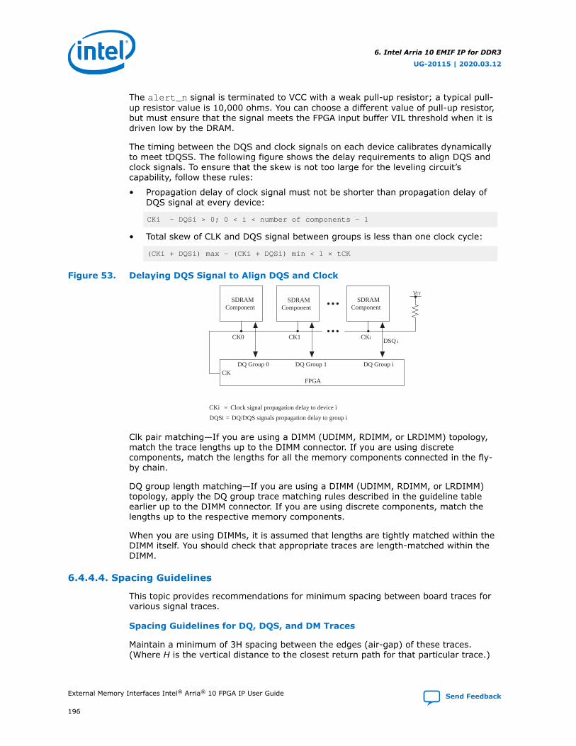
• Sequencer components
• PLL and PHY clock trees
3. Intel Arria 10 EMIF IP Product Architecture
UG-20115 | 2020.03.12
External Memory Interfaces Intel® Arria® 10 FPGA IP User Guide Send Feedback
• 48 pins, organized into four I/O lanes of 12 pins each
Figure 4. I/O Bank Architecture
Memory C ontroller
S equencer
P LL
C lock P hase Alignment
I/O Lane 3 Output Path Input Path
I/O Lane 2 Output Path Input Path
I/O Lane 1 Output Path Input Path
I/O Lane 0 Output Path Input Path
to / from bank above
to / from bank below
to / from FPGA core
I/O Bank
I/O Bank Usage
The pins in an I/O bank can serve as address and command pins, data pins, or clockand strobe pins for an external memory interface. You can implement a narrowinterface, such as a DDR3 or DDR4 x8 interface, with only a single I/O bank. A widerinterface, such as x72 or x144, can be implemented by configuring multiple adjacentbanks in a multi-bank interface. Any pins in a bank which are not used by the externalmemory interface remain available for use as general purpose I/O pins (of the samevoltage standard).
Every I/O bank includes a hard memory controller which you can configure for DDR3or DDR4. In a multi-bank interface, only the controller of one bank is active;controllers in the remaining banks are turned off to conserve power.
To use a multi-bank EMIF interface, you must observe the following rules:
• Designate one bank as the address and command bank.
• The address and command bank must contain all the address and command pins.
• The locations of individual address and command pins within the address andcommand bank must adhere to the pin map defined in the pin table— regardlessof whether you use the hard memory controller or not.
• If you do use the hard memory controller, the address and command bankcontains the active hard controller.
All the I/O banks in a column are capable of functioning as the address and commandbank. However, for minimal latency, you should select the center-most bank of theinterface as the address and command bank.
3. Intel Arria 10 EMIF IP Product Architecture
UG-20115 | 2020.03.12
Send Feedback External Memory Interfaces Intel® Arria® 10 FPGA IP User Guide
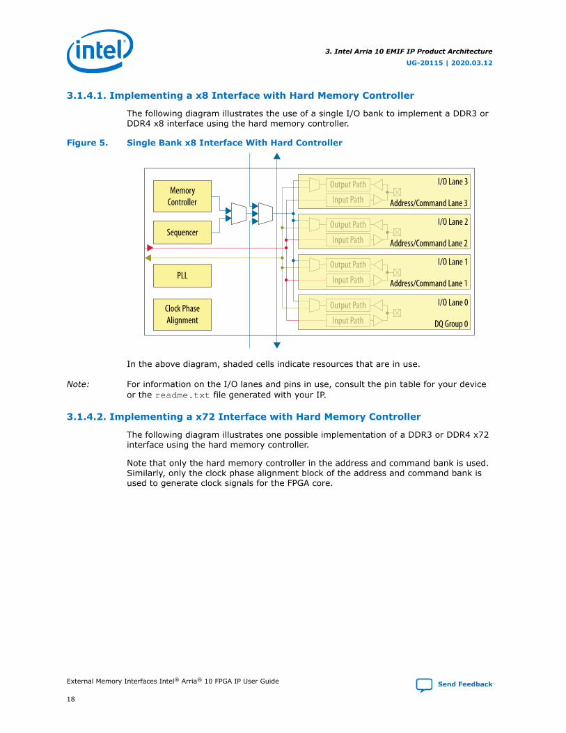
3.1.4.1. Implementing a x8 Interface with Hard Memory Controller
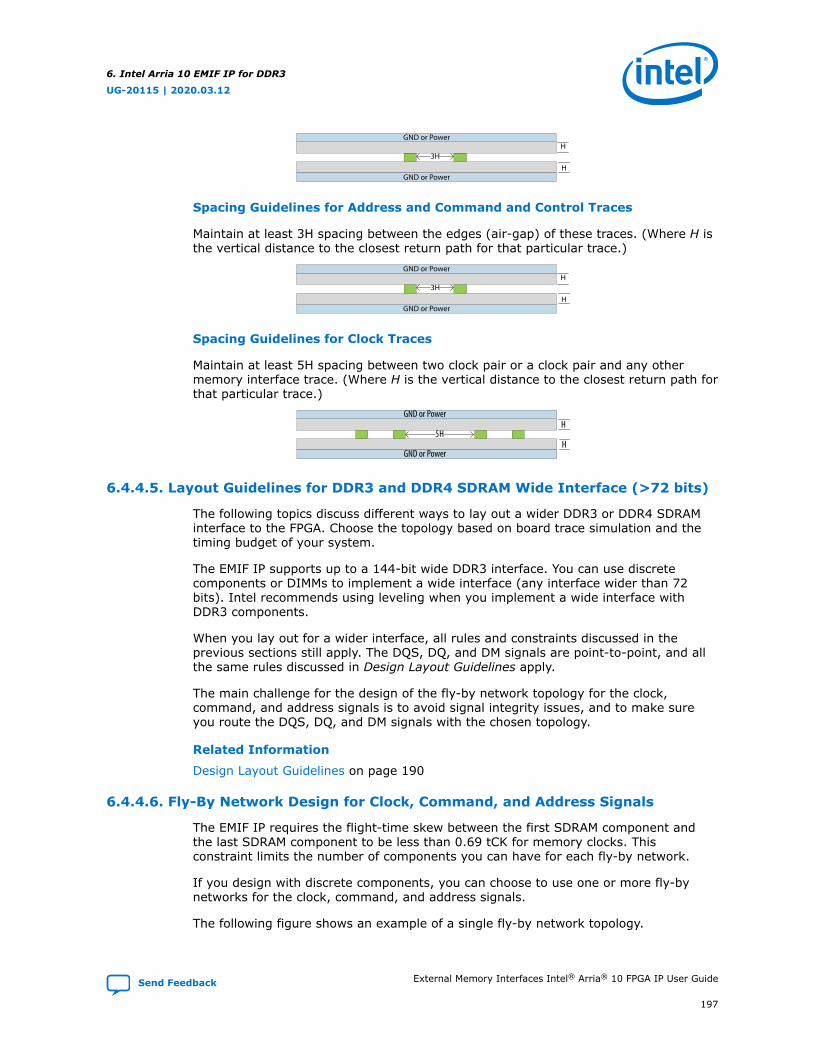
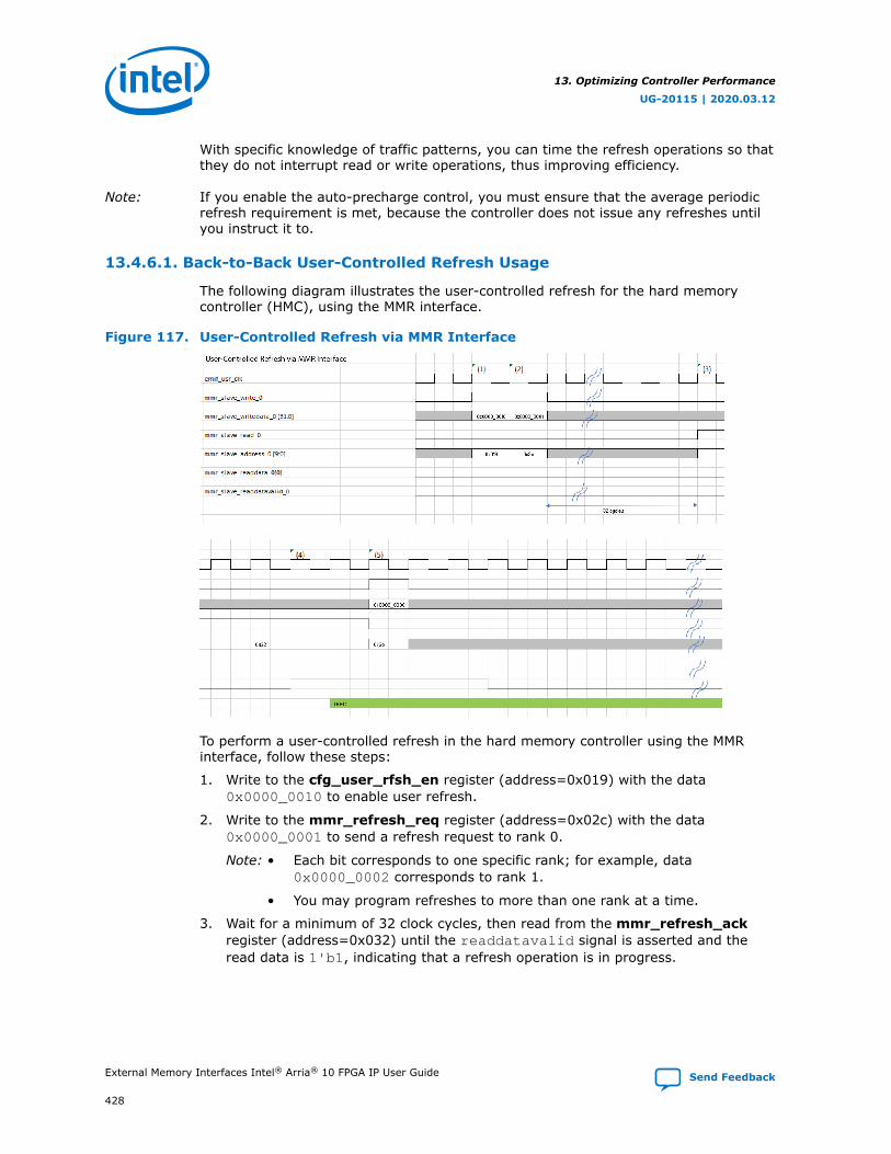
The following diagram illustrates the use of a single I/O bank to implement a DDR3 orDDR4 x8 interface using the hard memory controller.
Figure 5. Single Bank x8 Interface With Hard Controller
MemoryController
Clock PhaseAlignment
Sequencer
PLL
Output Path
Input Path
Output Path
Input Path
Output Path
Input Path
Output Path
Input Path
I/O Lane 3
Address/Command Lane 3
I/O Lane 2
Address/Command Lane 2
I/O Lane 1
Address/Command Lane 1
I/O Lane 0
DQ Group 0
In the above diagram, shaded cells indicate resources that are in use.
Note: For information on the I/O lanes and pins in use, consult the pin table for your deviceor the readme.txt file generated with your IP.
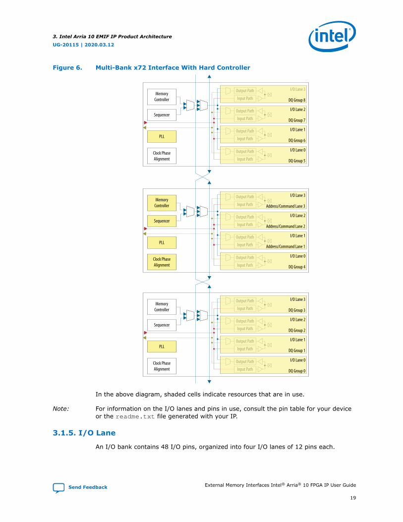
3.1.4.2. Implementing a x72 Interface with Hard Memory Controller
The following diagram illustrates one possible implementation of a DDR3 or DDR4 x72interface using the hard memory controller.
Note that only the hard memory controller in the address and command bank is used.Similarly, only the clock phase alignment block of the address and command bank isused to generate clock signals for the FPGA core.
3. Intel Arria 10 EMIF IP Product Architecture
UG-20115 | 2020.03.12
External Memory Interfaces Intel® Arria® 10 FPGA IP User Guide Send Feedback
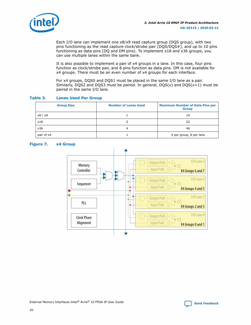
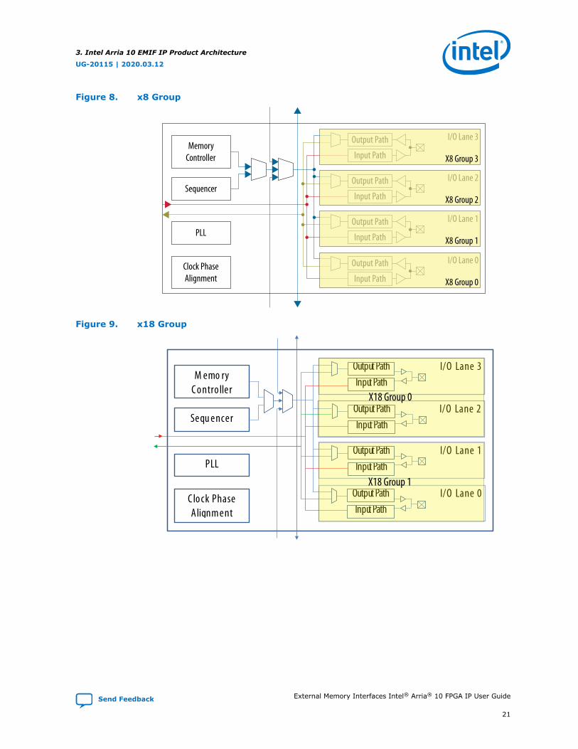
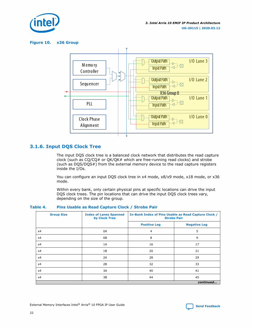
Each I/O lane can implement one x8/x9 read capture group (DQS group), with twopins functioning as the read capture clock/strobe pair (DQS/DQS#), and up to 10 pinsfunctioning as data pins (DQ and DM pins). To implement x18 and x36 groups, youcan use multiple lanes within the same bank.
It is also possible to implement a pair of x4 groups in a lane. In this case, four pinsfunction as clock/strobe pair, and 8 pins function as data pins. DM is not available forx4 groups. There must be an even number of x4 groups for each interface.
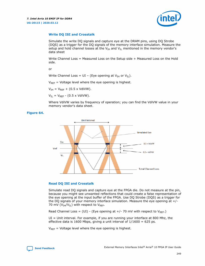
For x4 groups, DQS0 and DQS1 must be placed in the same I/O lane as a pair.Similarly, DQS2 and DQS3 must be paired. In general, DQS(x) and DQS(x+1) must bepaired in the same I/O lane.
Table 3. Lanes Used Per Group
Group Size Number of Lanes Used Maximum Number of Data Pins perGroup
x8 / x9 1 10
x18 2 22
x36 4 46
pair of x4 1 4 per group, 8 per lane
Figure 7. x4 Group
MemoryController
Clock PhaseAlignment
Sequencer
PLL
I/O Lane 3Output Path
Input Path
I/O Lane 2Output Path
Input Path
I/O Lane 1Output Path
Input Path
I/O Lane 0Output Path
Input Path
X4 Groups 6 and 7
X4 Groups 4 and 5
X4 Groups 2 and 3
X4 Groups 0 and 1
3. Intel Arria 10 EMIF IP Product Architecture
UG-20115 | 2020.03.12
External Memory Interfaces Intel® Arria® 10 FPGA IP User Guide Send Feedback
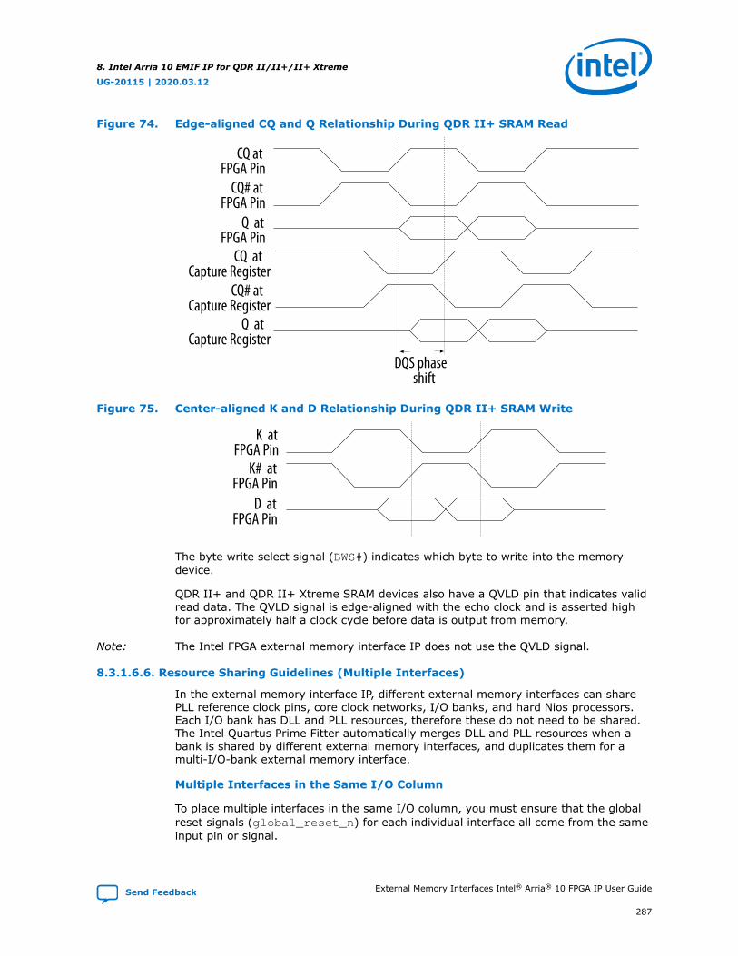
The input DQS clock tree is a balanced clock network that distributes the read captureclock (such as CQ/CQ# or QK/QK# which are free-running read clocks) and strobe(such as DQS/DQS#) from the external memory device to the read capture registersinside the I/Os.
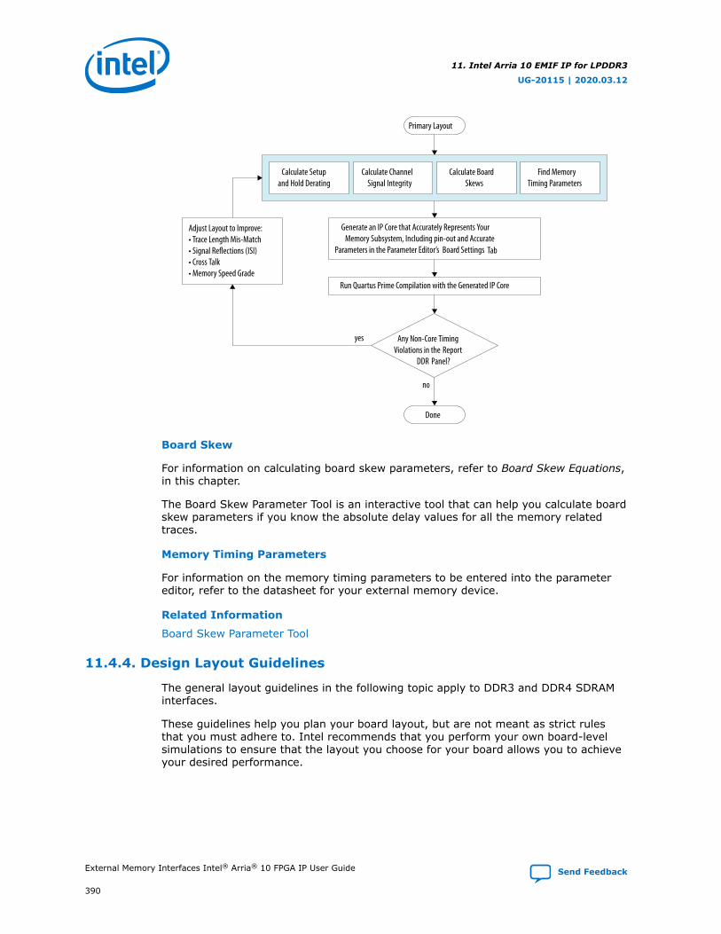
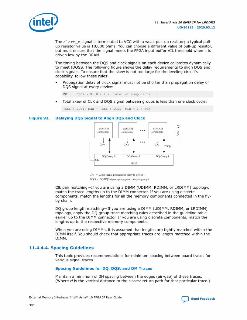
You can configure an input DQS clock tree in x4 mode, x8/x9 mode, x18 mode, or x36mode.
Within every bank, only certain physical pins at specific locations can drive the inputDQS clock trees. The pin locations that can drive the input DQS clock trees vary,depending on the size of the group.
In-Bank Index of Pins Usable as Read Capture Clock /Strobe Pair
Positive Leg Negative Leg
x8 / x9 0 4 5
x8 / x9 1 16 17
x8 / x9 2 28 29
x8 / x9 3 40 41
x18 0, 1 12 13
x18 2, 3 36 37
x36 0, 1, 2, 3 20 21
3.1.7. PHY Clock Tree
Dedicated high-speed clock networks drive I/Os in Intel Arria 10 external memoryinterfaces. Each PHY clock network spans only one bank.
The relatively short span of the PHY clock trees results in low jitter and low duty-cycledistortion, maximizing the data valid window.
All Intel Arria 10 external memory interfaces use the PHY clock trees.
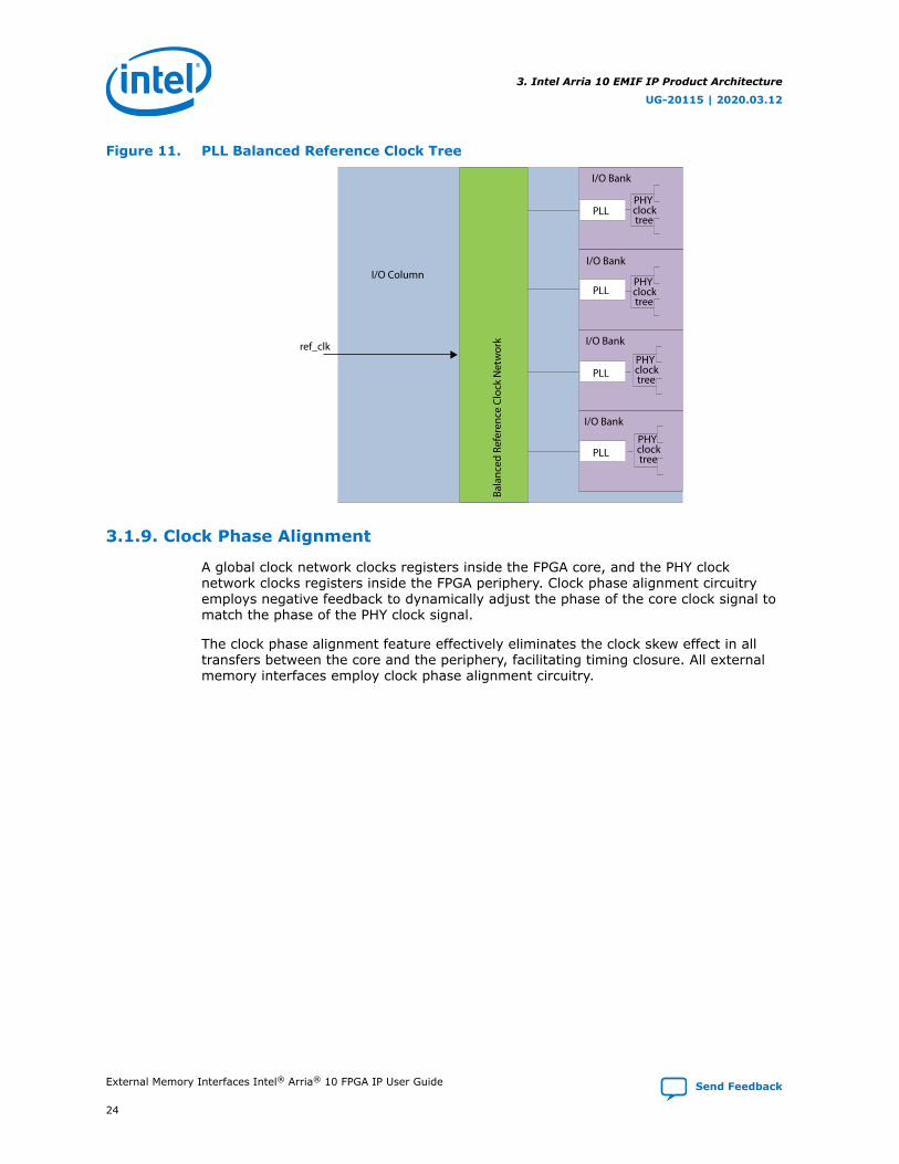
3.1.8. PLL Reference Clock Networks
Each I/O bank includes a PLL that can drive the PHY clock trees of that bank, throughdedicated connections. In addition to supporting EMIF-specific functions, such PLLscan also serve as general-purpose PLLs for user logic.
External memory interfaces that span multiple banks use the PLL in each bank. TheIntel Arria 10 architecture allows for relatively short PHY clock networks, reducingjitter and duty-cycle distortion.
In a multi-bank interface, the clock outputs of individual PLLs must remain in phase;this is achieved by the following mechanisms:
• A single PLL reference clock source feeds all PLLs. The reference clock signalreaches the PLLs by a balanced PLL reference clock tree. The Intel Quartus Primesoftware automatically configures the PLL reference clock tree so that it spans thecorrect number of banks.
• The IP sets the PLL M and N values appropriately to maintain synchronizationamong the clock dividers across the PLLs. This requirement restricts the legal PLLreference clock frequencies for a given memory interface frequency and clock rate.The parameter editor automatically calculates and displays the set of legal PLLreference clock frequencies. If you plan to use an on-board oscillator, you mustensure that its frequency matches the PLL reference clock frequency that youselect from the displayed list. The correct M and N values of the PLLs are setautomatically based on the PLL reference clock frequency that you select.
Note: The PLL reference clock pin may be placed in the address and command I/O bank or ina data I/O bank, there is no implication on timing.
3. Intel Arria 10 EMIF IP Product Architecture
UG-20115 | 2020.03.12
Send Feedback External Memory Interfaces Intel® Arria® 10 FPGA IP User Guide
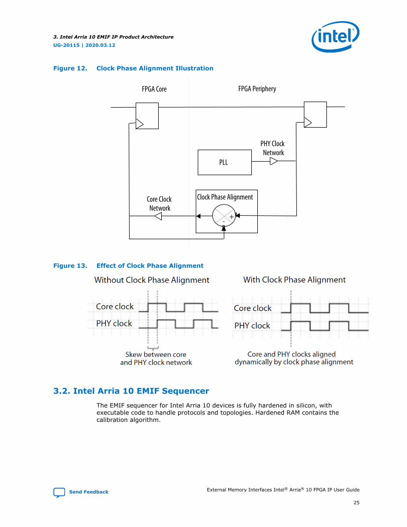
A global clock network clocks registers inside the FPGA core, and the PHY clocknetwork clocks registers inside the FPGA periphery. Clock phase alignment circuitryemploys negative feedback to dynamically adjust the phase of the core clock signal tomatch the phase of the PHY clock signal.
The clock phase alignment feature effectively eliminates the clock skew effect in alltransfers between the core and the periphery, facilitating timing closure. All externalmemory interfaces employ clock phase alignment circuitry.
3. Intel Arria 10 EMIF IP Product Architecture
UG-20115 | 2020.03.12
External Memory Interfaces Intel® Arria® 10 FPGA IP User Guide Send Feedback
The EMIF sequencer for Intel Arria 10 devices is fully hardened in silicon, withexecutable code to handle protocols and topologies. Hardened RAM contains thecalibration algorithm.
3. Intel Arria 10 EMIF IP Product Architecture
UG-20115 | 2020.03.12
Send Feedback External Memory Interfaces Intel® Arria® 10 FPGA IP User Guide
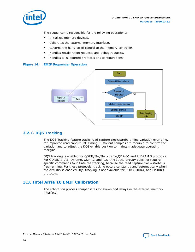
The sequencer is responsible for the following operations:
• Initializes memory devices.
• Calibrates the external memory interface.
• Governs the hand-off of control to the memory controller.
• Handles recalibration requests and debug requests.
• Handles all supported protocols and configurations.
Figure 14. EMIF Sequencer Operation
Discover EMIFs in column
Initialize external memory
Calibrate interface
Hand-off
Processed allinterfaces? Yes
No
Start
House-keepingtasks
Sequencersoftware Data
3.2.1. DQS Tracking
The DQS Tracking feature tracks read capture clock/strobe timing variation over time,for improved read capture I/O timing. Sufficient samples are required to confirm thevariation and to adjust the DQS-enable position to maintain adequate operatingmargins.
DQS tracking is enabled for QDRII/II+/II+ Xtreme,QDR-IV, and RLDRAM 3 protocols.For QDRII/II+/II+ Xtreme, QDR-IV, and RLDRAM 3, the circuity does not requirespecific commands to initiate the tracking, because the read capture clock/strobe isfree-running. For these protocols, tracking occurs constantly and automatically whenthe circuitry is enabled.DQS tracking is not available for DDR3, DDR4, and LPDDR3protocols.
3.3. Intel Arria 10 EMIF Calibration
The calibration process compensates for skews and delays in the external memoryinterface.
3. Intel Arria 10 EMIF IP Product Architecture
UG-20115 | 2020.03.12
External Memory Interfaces Intel® Arria® 10 FPGA IP User Guide Send Feedback
The calibration process enables the system to compensate for the effects of factorssuch as the following:
• Timing and electrical constraints, such as setup/hold time and Vref variations.
• Circuit board and package factors, such as skew, fly-by effects, and manufacturingvariations.
• Environmental uncertainties, such as variations in voltage and temperature.
• The demanding effects of small margins associated with high-speed operation.
For a given external memory interface, calibration occurs in parallel for all DQS groupsand I/O banks. For an I/O column containing multiple external memory interfaces,there is no particular calibration order in relation to the interfaces; however, for agiven SRAM Object File (.sof), calibration will always occur in the same order.
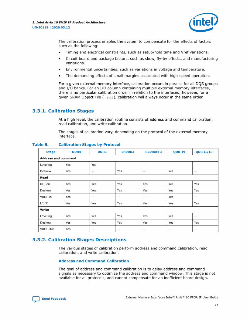
3.3.1. Calibration Stages
At a high level, the calibration routine consists of address and command calibration,read calibration, and write calibration.
The stages of calibration vary, depending on the protocol of the external memoryinterface.
Table 5. Calibration Stages by Protocol
Stage DDR4 DDR3 LPDDR3 RLDRAM 3 QDR-IV QDR II/II+
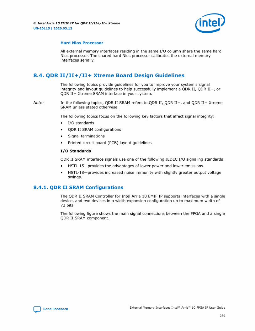
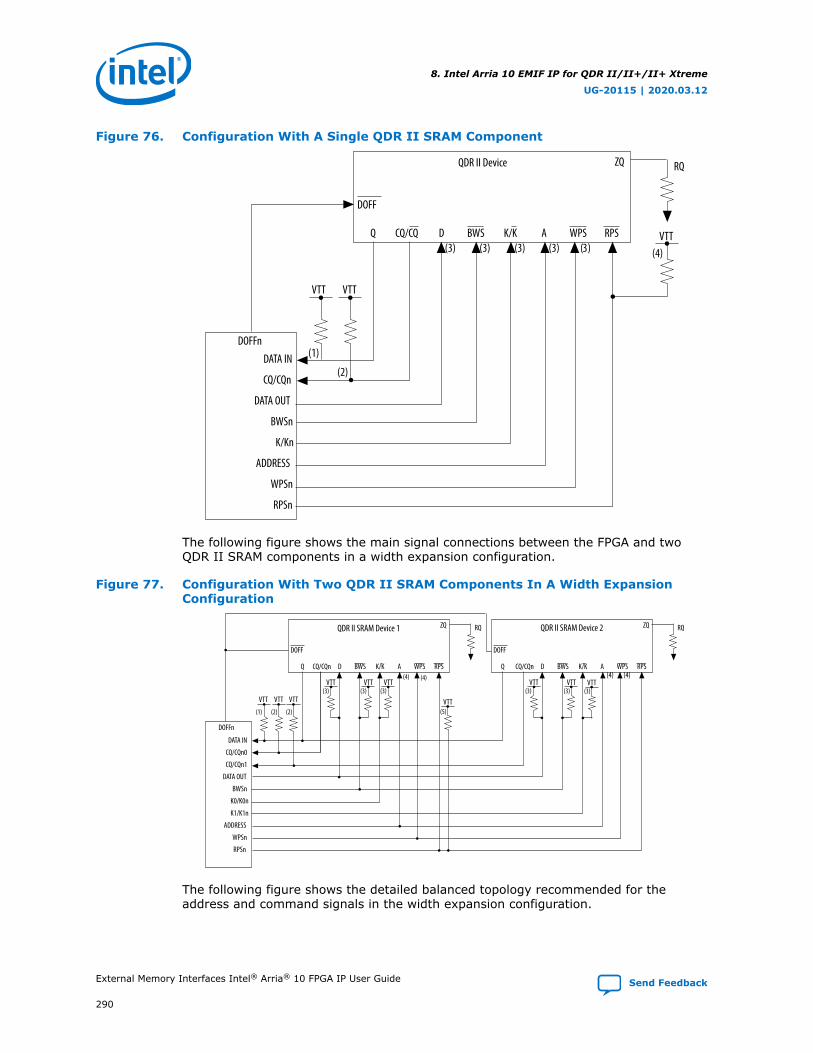
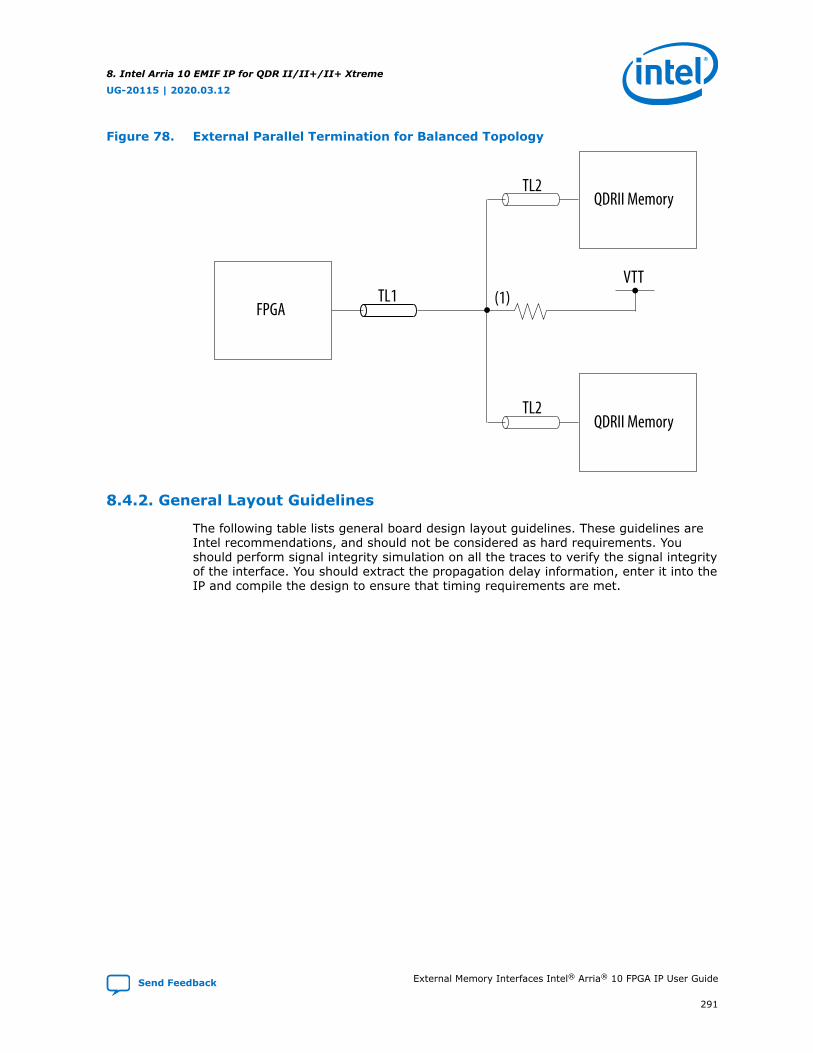
Address and command
Leveling Yes Yes — — — —
Deskew Yes — Yes — Yes —
Read
DQSen Yes Yes Yes Yes Yes Yes
Deskew Yes Yes Yes Yes Yes Yes
VREF-In Yes — — — Yes —
LFIFO Yes Yes Yes Yes Yes Yes
Write
Leveling Yes Yes Yes Yes Yes —
Deskew Yes Yes Yes Yes Yes Yes
VREF-Out Yes — — — — —
3.3.2. Calibration Stages Descriptions
The various stages of calibration perform address and command calibration, readcalibration, and write calibration.
Address and Command Calibration
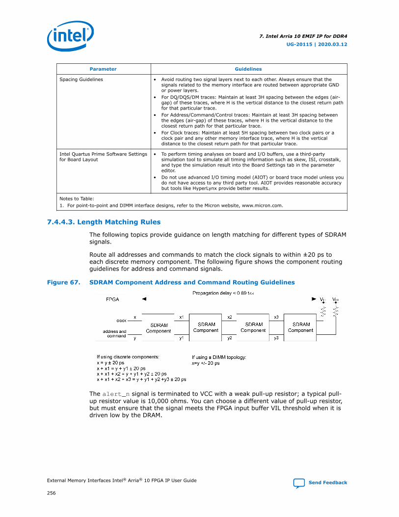
The goal of address and command calibration is to delay address and commandsignals as necessary to optimize the address and command window. This stage is notavailable for all protocols, and cannot compensate for an inefficient board design.
3. Intel Arria 10 EMIF IP Product Architecture
UG-20115 | 2020.03.12
Send Feedback External Memory Interfaces Intel® Arria® 10 FPGA IP User Guide
Address and command calibration consists of the following parts:
• Leveling calibration— Centers the CS# signal and the entire address andcommand bus, relative to the CK clock. This operation is available only for DDR3and DDR4 interfaces.
• Deskew calibration— Provides per-bit deskew for the address and command bus(except CS#), relative to the CK clock. This operation is available for DDR4 andQDR-IV interfaces only.
Read Calibration
Read calibration consists of the following parts:
• DQSen calibration— Calibrates the timing of the read capture clock gating andungating, so that the PHY can gate and ungate the read clock at precisely thecorrect time—if too early or too late, data corruption can occur. The algorithm forthis stage varies, depending on the memory protocol.
• Deskew calibration— Performs per-bit deskew of read data relative to the readstrobe or clock.
• VREF-IN calibration— Calibrates the Vref level at the FPGA.
• LFIFO calibration: Normalizes differences in read delays between groups due tofly-by, skews, and other variables and uncertainties.
Write Calibration
Write calibration consists of the following parts:
• Leveling calibration— Aligns the write strobe and clock to the memory clock, tocompensate for skews, especially those associated with fly-by topology. Thealgorithm for this stage varies, depending on the memory protocol.
• Deskew calibration— Performs per-bit deskew of write data relative to the writestrobe and clock.
• VREF-Out calibration— Calibrates the VREF level at the memory device.
3.3.3. Calibration Algorithms
The calibration algorithms sometimes vary, depending on the targeted memoryprotocol.
Address and Command CalibrationAddress and command calibration consists of the following parts:
3. Intel Arria 10 EMIF IP Product Architecture
UG-20115 | 2020.03.12
External Memory Interfaces Intel® Arria® 10 FPGA IP User Guide Send Feedback
• Leveling calibration— (DDR3 and DDR4 only) Toggles the CS# and CAS# signalsto send read commands while keeping other address and command signalsconstant. The algorithm monitors for incoming DQS signals, and if the DQS signaltoggles, it indicates that the read commands have been accepted. The algorithmthen repeats using different delay values, to find the optimal window.
• Deskew calibration— (DDR4, QDR-IV, and LPDDR3 only)
— (DDR4) Uses the DDR4 address and command parity feature. The FPGA sendsthe address and command parity bit, and the DDR4 memory device respondswith an alert signal if the parity bit is detected. The alert signal from thememory device tells the FPGA that the parity bit was received.
Deskew calibration requires use of the PAR/ALERT# pins, so you should notomit these pins from your design. One limitation of deskew calibration is thatit cannot deskew ODT and CKE pins.
— (QDR-IV) Uses the QDR-IV loopback mode. The FPGA sends address andcommand signals, and the memory device sends back the address andcommand signals which it captures, via the read data pins. The returnedsignals indicate to the FPGA what the memory device has captured. Deskewcalibration can deskew all synchronous address and command signals.
— (LPDDR3) Uses the LPDDR3 CA training mode. The FPGA sends signals ontothe LPDDR3 CA bus, and the memory device sends back those signals that itcaptures, via the DQ pins. The returned signals indicate to the FPGA what thememory device has captured. Deskew calibration can deskew all signals on theCA bus. The remaining command signals (CS, CKE, and ODT) are calibratedbased on the average of the deskewed CA bus.
3. Intel Arria 10 EMIF IP Product Architecture
UG-20115 | 2020.03.12
Send Feedback External Memory Interfaces Intel® Arria® 10 FPGA IP User Guide
• DQSen calibration— (DDR3, DDR4, LPDDR3, RLDRAMx and QDRx) DQSencalibration occurs before Read deskew, therefore only a single DQ bit is required topass in order to achieve a successful read pass.
— (DDR3, DDR4, and LPDDR3) The DQSen calibration algorithm searches theDQS preamble using a hardware state machine. The algorithm sends manyback-to-back reads with a one clock cycle gap between. The hardware statemachine searches for the DQS gap while sweeping DQSen delay values. thealgorithm then increments the VFIFO value, and repeats the process until apattern is found. The process is then repeated for all other read DQS groups.
— (RLDRAMx and QDRx) The DQSen calibration algorithm does not use ahardware state machine; rather, it calibrates cycle-level delays using softwareand subcycle delays using DQS tracking hardware. The algorithm requiresgood data in memory, and therefore relies on guaranteed writes. (Writing aburst of 0s to one location, and a burst of 1s to another; back-to-back readsfrom these two locations are used for read calibration.)
The algorithm enables DQS tracking to calibrate the phase component of DQSenable. It then issues a guaranteed write, followed by back-to-back reads. Thealgorithm sweeps DQSen values cycle by cycle until the read operationsucceeds. The process is then repeated for all other read groups.
• Deskew calibration— Read deskew calibration is performed before write leveling,and must be performed at least twice: once before write calibration, using simpledata patterns from guaranteed writes, and again after write calibration, usingcomplex data patterns.
The deskew calibration algorithm performs a guaranteed write, and then sweepsdqs_in delay values from low to high, to find the right edge of the read window.The algorithm then sweeps dq-in delay values low to high, to find the left edge ofthe read window. Updated dqs_in and dq_in delay values are then applied tocenter the read window. The algorithm then repeats the process for all data pins.
• Vref-In calibration— Read Vref-In calibration begins by programming Vref-Inwith an arbitrary value. The algorithm then sweeps the Vref-In value from thestarting value to both ends, and measures the read window for each value. Thealgorithm selects the Vref-In value which provides the maximum read window.
• LFIFO calibration— Read LFIFO calibration normalizes read delays between groups.The PHY must present all data to the controller as a single data bus. The LFIFOlatency should be large enough for the slowest read data group, and large enoughto allow proper synchronization across FIFOs.
3. Intel Arria 10 EMIF IP Product Architecture
UG-20115 | 2020.03.12
External Memory Interfaces Intel® Arria® 10 FPGA IP User Guide Send Feedback
• Leveling calibration— Write leveling calibration aligns the write strobe and clock tothe memory clock, to compensate for skews. In general, leveling calibration tries avariety of delay values to determine the edges of the write window, and thenselects an appropriate value to center the window. The details of the algorithmvary, depending on the memory protocol.
— (DDRx, LPDDR3) Write leveling occurs before write deskew, therefore only onesuccessful DQ bit is required to register a pass. Write leveling staggers the DQbus to ensure that at least one DQ bit falls within the valid write window.
— (RLDRAMx) Optimizes for the CK versus DK relationship.
— (QDR-IV) Optimizes for the CK versus DK relationship. Is covered by addressand command deskew using the loopback mode.
— (QDR II/II+/Xtreme) The K clock is the only clock, therefore write leveling isnot required.
• Deskew calibration— Performs per-bit deskew of write data relative to the writestrobe and clock. Write deskew calibration does not change dqs_out delays; thewrite clock is aligned to the CK clock during write leveling.
• VREF-Out calibration— (DDR4) Calibrates the VREF level at the memory device.The VREF-Out calibration algorithm is similar to the VREF-In calibration algorithm.
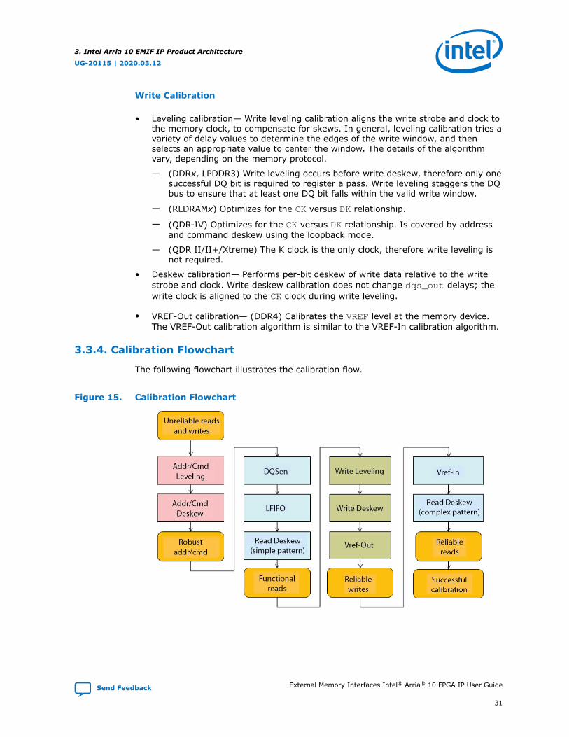
3.3.4. Calibration Flowchart
The following flowchart illustrates the calibration flow.
Figure 15. Calibration Flowchart
3. Intel Arria 10 EMIF IP Product Architecture
UG-20115 | 2020.03.12
Send Feedback External Memory Interfaces Intel® Arria® 10 FPGA IP User Guide
Periodic OCT recalibration improves the accuracy of the on-chip termination valuesused by DDR4 Pseudo-open Drain (POD) I/Os. This feature periodically invokes theuser-mode OCT calibration engine and updates the I/O buffer termination settings tocompensate for variations in calibrated OCT settings caused by large changes indevice operating temperature.
This feature is automatically enabled for DDR4 memory interfaces unless the IP doesnot meet the technical requirements, or if you explicitly disable the feature in theparameter editor.
3.4.1. Operation
The Periodic OCT recalibration engine refreshes the calibrated OCT settings for DDR4I/O buffers every 500ms. To ensure data integrity, there is a momentary pause in usertraffic as the OCT settings are refreshed; however, the process of OCT calibration isdecoupled from the actual update to the I/O buffers, to minimize disruption of usertraffic.
The calibration process uses the external RZQ reference resistor to determine theoptimal settings for the I/O buffer, to meet the specified calibrated I/O standards onthe FPGA. OCT Calibration only affects the I/O pin that is connected to the RZQresistor; therefore, memory traffic is not interrupted during the calibration phase.
Upon completion of the calibration process, the updated calibration settings areapplied to the I/O buffers. The memory traffic is halted momentarily by placing thememory into self-refresh mode; this ensures that the data bus is idle and no glitchesare created by the I/O buffers during the buffer update. The buffer is updated as soonas the memory enters self-refresh mode. The memory interface exits self-refreshmode when the buffer update is complete and new read or write requests are detectedon the Avalon bus. The controller remains in self-refresh mode until a new commandis detected. OCT calibration continues to occur even if the memory is still in selfrefresh mode. Upon detection of a new command, the controller issues a self-refreshexit command to the memory, followed by a memory-side ZQ calibration shortduration (ZQCS) command. Memory traffic resumes when the memory DLL has re-locked.
If you disable the periodic OCT recalibration engine, the calibration process occursonly once during device configuration. In this operating mode, the calibrated OCTsettings can vary across temperature as specified by the calibration accuracy rangesfor the device. The DDR external timing report automatically factors in the effect ofenabling or disabling the periodic OCT recalibration engine when calculating the totalamount of external I/O transfer margin.
3.4.2. Technical Restrictions
Certain criteria must be met in order to use periodic OCT recalibration.
3. Intel Arria 10 EMIF IP Product Architecture
UG-20115 | 2020.03.12
External Memory Interfaces Intel® Arria® 10 FPGA IP User Guide Send Feedback
The periodic OCT recalibration engine is enabled only when all of the following criteriaare met:
• The memory interface is configured to use the Altera Hard Memory Controller forDDR4.
• The memory interface is configured for either DDR4 UDIMM or componenttopologies. RDIMM and LRDIMM topologies are not supported.
• The memory interface is not used with the hardened processor subsystem.
• The memory interface does not use Ping-Pong PHY.
• The memory interface does not use calibrated I/O standards for address,command, or clock signals.
• The memory interface uses calibrated I/O standards for the data bus.
• The memory does not use the memory mapped register (MMR) interface of theHMC, including ECC modes.
• You have not explicitly disabled periodic OCT recalibration in the parameter editor.
• The specified device is a production level device (that is, not an ES/ES2/ES3 classdevice).
Periodic OCT recalibration requires that each EMIF instance in the design employ adedicated RZQ resistor. Because this restriction cannot be detected at IP generationtime, you must explicitly disable the periodic OCT recalibration engine for a giveninterface if it shares an RZQ resistor with another interface. Ensure that you observethis restriction when automatically upgrading EMIF IP from older versions of the IntelQuartus Prime software.
3.4.3. Efficiency Impact
The Periodic OCT recalibration engine must interrupt user traffic for a short period oftime in order to update I/O buffer termination settings.
The exact flow of operations executed by the recalibration engine that affects memorytraffic is described below:
1. Enter Self-Refresh Mode. The EMIF calibration CPU triggers self-refresh entry onthe hard memory controller. The controller flushes all pending operations,precharges all banks and issues the self-refresh command. This operationintroduces a delay of approximately 25 Memory clock cycles (precharge all andself-refresh entry commands).
2. Confirm Self-Refresh Mode. The EMIF calibration CPU polls the hard memorycontroller to confirm that the clocks have stopped. This operation introduces nodelay.
3. Issue codeword update. The EMIF calibration CPU triggers user-mode OCT logic toupdate code words. This operation introduces a delay of 50-100ns, depending onthe device speed grade.
3. Intel Arria 10 EMIF IP Product Architecture
UG-20115 | 2020.03.12
Send Feedback External Memory Interfaces Intel® Arria® 10 FPGA IP User Guide
4. Allow Exit Self-Refresh Mode. The EMIF calibration CPU enables automatic self-refresh exit logic. This operation introduces a delay of 50-100ns, depending on thedevice speed grade.
5. Wait for Memory Traffic. The hard memory controller waits for an incoming read orwrite command on the Avalon bus. The delay introduced by this operation varies,depending on the user application.
6. Exit Self Refresh Mode. The hard memory controller issues the Self-Refresh Exitcommand and a simultaneous memory-side RZQ calibration (ZQCS) command.The delay introduced by this operation varies according to the device speed bin(up to ~1000 memory clock cycles for fastest memory devices).
The efficiency impact on throughput-sensitive work loads is less than one percent,even under worst-case scenarios with all banks active. However, be aware that thefirst command issued after the hard memory controller exits self-refresh mode willincur the latency overhead of waiting for the memory DLL to re-lock when the Self-Refresh Exit command is issued by the hard memory controller. Contact Intel FPGATechnical Services for information on how to manually trigger or inhibit periodic OCTupdates for applications that are sensitive to latency.
3.5. Intel Arria 10 EMIF Controller
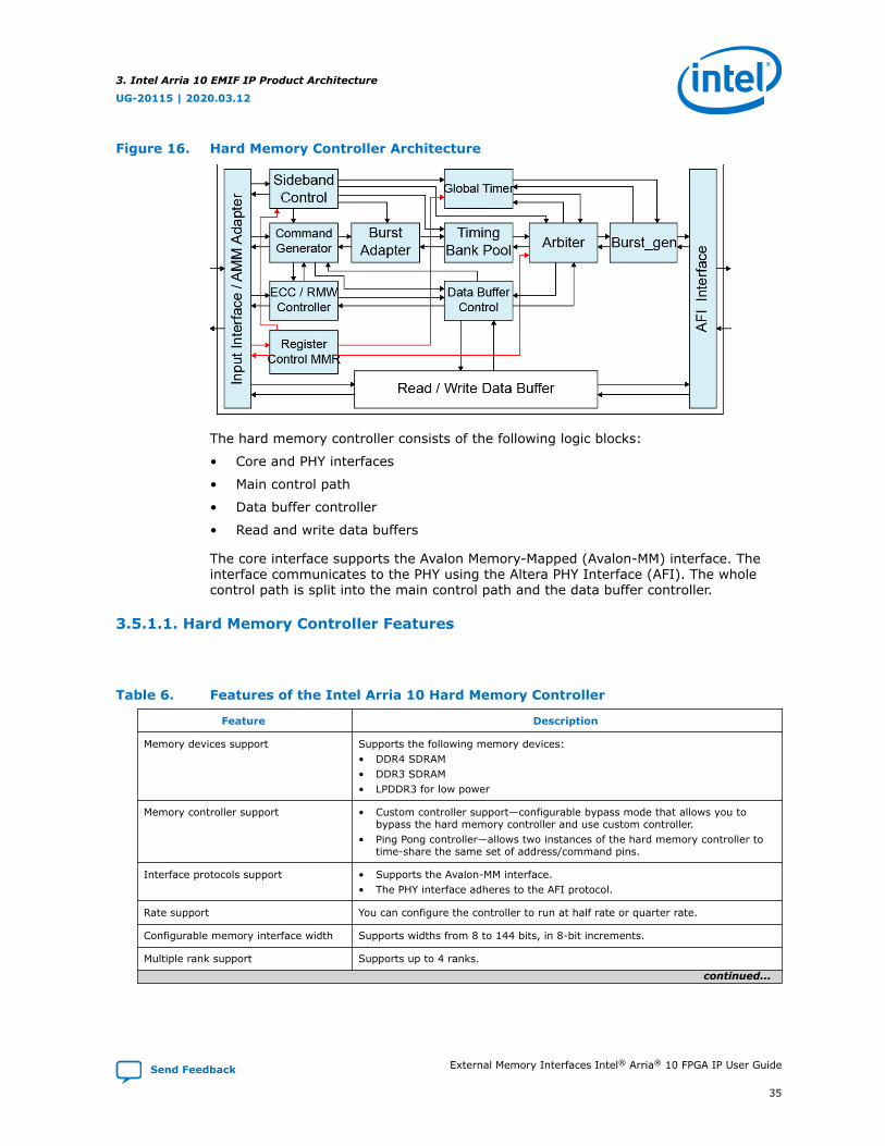
3.5.1. Hard Memory Controller
The Intel Arria 10 hard memory controller is designed for high speed, highperformance, high flexibility, and area efficiency. The Intel Arria 10 hard memorycontroller supports DDR3, DDR4, and LPDDR3 memory standards.
The hard memory controller implements efficient pipelining techniques and advanceddynamic command and data reordering algorithms to improve bandwidth usage andreduce latency, providing a high performance solution.
The controller architecture is modular and fits in a single I/O bank. The structureallows you to:
• Configure each I/O bank as either:
— A control path that drives all the address and command pins for the memoryinterface.
— A data path that drives up to 32 data pins for DDR-type interfaces.
• Place your memory controller in any location.
• Pack up multiple banks together to form memory interfaces of different widths upto 144 bits.
• Bypass the hard memory controller and use your own custom IP if required.
3. Intel Arria 10 EMIF IP Product Architecture
UG-20115 | 2020.03.12
External Memory Interfaces Intel® Arria® 10 FPGA IP User Guide Send Feedback
The hard memory controller consists of the following logic blocks:
• Core and PHY interfaces
• Main control path
• Data buffer controller
• Read and write data buffers
The core interface supports the Avalon Memory-Mapped (Avalon-MM) interface. Theinterface communicates to the PHY using the Altera PHY Interface (AFI). The wholecontrol path is split into the main control path and the data buffer controller.
3.5.1.1. Hard Memory Controller Features
Table 6. Features of the Intel Arria 10 Hard Memory Controller
Feature Description
Memory devices support Supports the following memory devices:• DDR4 SDRAM• DDR3 SDRAM• LPDDR3 for low power
Memory controller support • Custom controller support—configurable bypass mode that allows you tobypass the hard memory controller and use custom controller.
• Ping Pong controller—allows two instances of the hard memory controller totime-share the same set of address/command pins.
Interface protocols support • Supports the Avalon-MM interface.• The PHY interface adheres to the AFI protocol.
Rate support You can configure the controller to run at half rate or quarter rate.
Configurable memory interface width Supports widths from 8 to 144 bits, in 8-bit increments.
Multiple rank support Supports up to 4 ranks.
continued...
3. Intel Arria 10 EMIF IP Product Architecture
UG-20115 | 2020.03.12
Send Feedback External Memory Interfaces Intel® Arria® 10 FPGA IP User Guide
Burst adaptor Able to accept bursts of any size up to a maximum burst length of 127 on thelocal interface of the controller and map the bursts to efficient memorycommands.Note: For applications that must adhere strictly to the Avalon-MM specification,
the maximum burst length is 64.
Efficiency optimization features • Open-page policy—by default, data traffic is closed-page on every access.However, the controller keeps a row open based on incoming traffic, whichcan improve controller efficiency, especially for random traffic.
• Preemptive bank management—the controller can issue bank managementcommands early, to ensure that the required row is already open when theread or write occurs.
• Data reordering—the controller reorders read and write commands.• Additive latency—the controller can issue a READ/WRITE command after the
ACTIVATE command to the memory bank, before tRCD, which increases thecommand efficiency
User requested priority You can assign priority to commands. This feature allows you to specify thathigher priority commands get issued earlier to reduce latency.
Starvation counter Ensures all requests are served after a predefined time out period, which ensuresthat low priority accesses are not left behind while reordering data for efficiency.
Timing for address/command bus To maximize command bandwidth, you can double the number of memorycommands in one controller clock cycle:• Quasi-1T addressing for half-rate address/command bus• Quasi-2T addressing for quarter-rate address/command bus
Bank interleaving Able to issue read or write commands continuously to random addresses. Youmust correctly cycle the bank addresses.
On-die termination The controller controls the on-die termination signal for the memory. This featureimproves signal integrity and simplifies your board design.
Refresh features • User-controlled refresh timing—optionally, you can control when refreshesoccur. This allows you to prevent important read or write operations fromclashing with the refresh lock-out time.
• Per-rank refresh—allows refresh for each individual rank.• Controller-controlled refresh.
ECC support • 8-bit ECC code; single error correction, double error detection (SECDED).• User ECC supporting pass-through user ECC bits as part of data bits.
Power saving features • Low-power modes (power down and self-refresh)—optionally, you can requestthat the controller put the memory into one of the two low-power states.
• Automatic power down—puts the memory device in power-down mode whenthe controller is idle. You can configure the idle waiting time.
• Memory clock gating.
Mode register set Access the memory mode register.
DDR4 features • Bank group support—supports different timing parameters for between bankgroups.
• Data Bus CRC—data bus encoding and decoding.• Command/Address parity—command and address bus parity check.• Alert reporting—responds to the error alert flag.• Multipurpose register access—supports multipurpose register access in serial
readout mode.• Fine granularity refresh—supports 1x, 2x, and 4x fixed refresh rates.
continued...
3. Intel Arria 10 EMIF IP Product Architecture
UG-20115 | 2020.03.12
External Memory Interfaces Intel® Arria® 10 FPGA IP User Guide Send Feedback
• Temperature-controlled refresh—adjusts the refresh rate according to atemperature range.
• Low-power auto self-refresh—operating-temperature-triggered autoadjustment to the self-refresh rate.
• Maximum power savings.
LPDDR3 features • Deep power-down mode—achieves maximum power reduction by eliminatingpower to the memory array. Data is not retained when the device enters deeppower-down mode.
• Partial array self-refresh.• Per-bank refresh.
ZQ calibration command Support long or short ZQ calibration command for DDR3 or DDR4.
3.5.1.2. Hard Memory Controller Main Control Path
The main control path performs the following functions:
• Contains the command processing pipeline.
• Monitors all the timing parameters.
• Keeps track of dependencies between memory access commands.
• Guards against memory access hazards.
Table 7. Main Control Path Components
Component Description
Input interface • Accepts memory access commands from the core logic at half or quarter rate.• Uses the Avalon-MM protocol.• You can connect the Avalon-MM interface to the AXI bus master in the Platform
Designer (formerly Qsys). To connect the Avalon-MM interface, implement the AXI busmaster as a Platform Designer component and connect the AXI bus master to theAvalon-MM slave. The Platform Designer interconnect performs the bus translationbetween the AXI and Avalon-MM bus interfaces.
• To support all bypass modes and keep the port count minimum, the super set of all portlists is used as the physical width. Ports are shared among the bypass modes.
Command generator andburst adapter
• Drains your commands from the input interface and feeds them to the timing bank pool.• If read-modify-write is required, inserts the necessary read-modify-write read and write
commands into the stream.• The burst adapter chops your arbitrary burst length to the number specified by the
memory types.
Timing Bank Pool • Key component in the memory controller.• Sets parallel queues to track command dependencies.• Signals the ready status of each command being tracked to the arbiter for the final
dispatch.• Big scoreboard structure. The number of entries is currently sized to 8 where it monitors
up to 8 commands at the same time.• Handles the memory access hazards such as Read After Write (RAW), Write After Read
(WAR), and Write After Write (WAW), while part of the timing constraints are beingtracked.
• High responsibility to assist the arbiter in implementing reordering:— Row command reordering (activate and pre-charge).— Column command reordering (read and write).
• When the pool is full, a flow control signal is sent back upstream to stall the traffic.
continued...
3. Intel Arria 10 EMIF IP Product Architecture
UG-20115 | 2020.03.12
Send Feedback External Memory Interfaces Intel® Arria® 10 FPGA IP User Guide
Arbiter • Enforces the arbitration rules.• Performs the final arbitration to select a command from all ready commands, and issues
the selected command to the memory.• Supports Quasi-1T mode for half rate and Quasi-2T mode for quarter rate.• For the quasi modes, a row command must be paired with a column command.
Global Timer Tracks the global timing constraints including:• tFAW—the Four Activates Window parameter that specifies the time period in which only
four activate commands are allowed.• tRRD—the delay between back-to-back activate commands to different banks.• Some of the bus turnaround time parameters.
MMR/IOCSR • The host of all the configuration registers.• Uses Avalon-MM bus to talk to the core.• Core logic can read and write all the configuration bits.• The debug bus is routed to the core through this block.
Sideband Executes the refresh and power down features.
ECC controller Although ECC encoding and decoding is performed in soft logic(1), the ECC controllermaintains the read-modify-write state machine in the hard solution.
AFI interface The memory controller communicates with the PHY using this interface.
3.5.1.3. Data Buffer Controller
The data buffer controller performs the following operations:
• Manages the read and write access to the data buffers:
— Provides the data storing pointers to the buffers when the write data isaccepted or the read return data arrives.
— Provides the draining pointer when the write data is dispatched to memory orthe read data is read out of the buffer and sent back to users.
• Satisfies the required write latency.
• If ECC support is enabled, assists the main control path to perform read-modify-write.
Data reordering is performed with the data buffer controller and the data buffers.
Each I/O bank contains two data buffer controller blocks for the data buffer lanes thatare split within each bank. To improve your timing, place the data buffer controllerphysically close to the I/O lanes.
3.5.2. Hard Memory Controller Rate Conversion Feature
The hard memory controller's rate conversion feature allows the hard memorycontroller and PHY to run at half-rate, even though user logic is configured to run atquarter-rate.
(1) ECC encoding and decoding is performed in soft logic to exempt the hard connection fromrouting data bits to a central ECC calculation location. Routing data to a central locationremoves the modular design benefits and reduces flexibility.
3. Intel Arria 10 EMIF IP Product Architecture
UG-20115 | 2020.03.12
External Memory Interfaces Intel® Arria® 10 FPGA IP User Guide Send Feedback
To facilitate timing closure, you may choose to clock your core user logic at quarter-rate, resulting in easier timing closure at the expense of increased area and latency.To improve efficiency and help reduce overall latency, you can run the hard memorycontroller and PHY at half rate.
The rate conversion feature converts traffic from the FPGA core to the hard memorycontroller from quarter-rate to half-rate, and traffic from the hard memory controllerto the FPGA core from half-rate to quarter-rate. From the perspective of user logicinside the FPGA core, the effect is the same as if the hard memory controller wererunning at quarter-rate.
The rate conversion feature is enabled automatically during IP generation whenever allof the following conditions are met:
• The hard memory controller is used.
• User logic runs at quarter-rate.
• The interface targets either an ES2 or production device.
• Running the hard memory controller at half-rate does not exceed the fMaxspecification of the hard memory controller and hard PHY.
When the rate conversion feature is enabled, you should see the following infomessage displayed in the IP generation GUI:PHY and controller running at 2x the frequency of user logic forimproved efficiency.
3.6. Hardware Resource Sharing Among Multiple EMIFs
Often, it is necessary or desirable to share resources between interfaces.
The following topics explain which hardware resources can be shared, and provideguidance for doing so.
3.6.1. I/O Aux Sharing
The I/O Aux contains a hard Nios-II processor and dedicated memory storing thecalibration software code and data.
When a column contains multiple memory interfaces, the hard Nios-II processorcalibrates each interface serially. Interfaces placed within the same I/O column alwaysshare the same I/O Aux. The Intel Quartus Prime Fitter handles I/O Aux sharingautomatically.
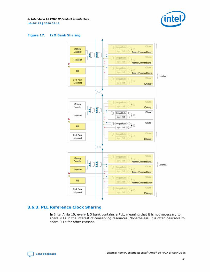
3.6.2. I/O Bank Sharing
Data lanes from multiple compatible interfaces can share a physical I/O bank toachieve a more compact pin placement. To share an I/O bank, interfaces must use thesame memory protocol, rate, frequency, I/O standard, and PLL reference clock signal.
3. Intel Arria 10 EMIF IP Product Architecture
UG-20115 | 2020.03.12
Send Feedback External Memory Interfaces Intel® Arria® 10 FPGA IP User Guide
• A bank cannot serve as the address and command bank for more than oneinterface. This means that lanes which implement address and command pins fordifferent interfaces cannot be allocated to the same physical bank.
Note: An exception to the above rule exists when two interfaces are configured ina Ping-Pong PHY fashion. In such a configuration, two interfaces share thesame set of address and command pins, effectively meaning that they sharethe same address and command tile.
• Pins within a lane cannot be shared by multiple memory interfaces.
• Pins that are not used by EMIF IP can serve as general-purpose I/Os of compatiblevoltage and termination settings.
• You can configure a bank as LVDS or as EMIF, but not both at the same time.
• Interfaces that share banks must reside at adjacent bank locations.
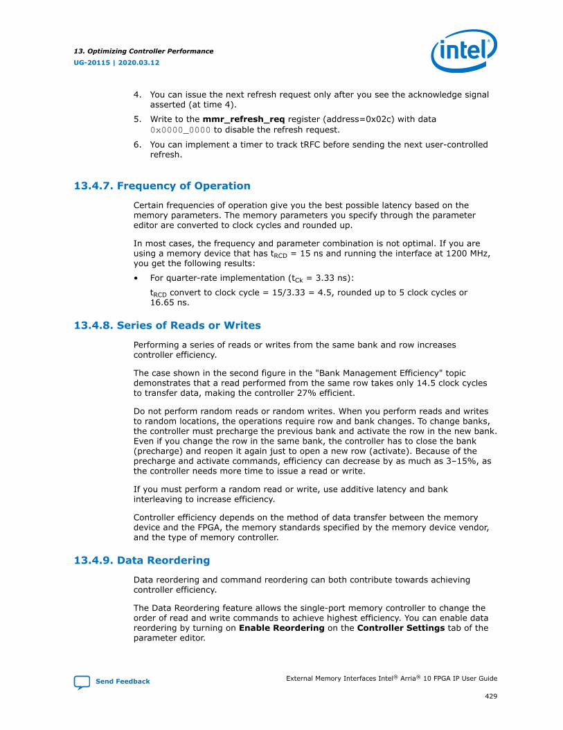
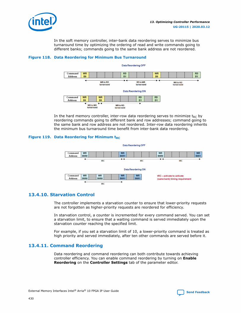
The following diagram illustrates two x16 interfaces sharing an I/O bank. The twointerfaces share the same clock phase alignment block, so that one core clock signalcan interact with both interfaces. Without sharing, the two interfaces would occupy atotal of four physical banks instead of three.
3. Intel Arria 10 EMIF IP Product Architecture
UG-20115 | 2020.03.12
External Memory Interfaces Intel® Arria® 10 FPGA IP User Guide Send Feedback
In Intel Arria 10, every I/O bank contains a PLL, meaning that it is not necessary toshare PLLs in the interest of conserving resources. Nonetheless, it is often desirable toshare PLLs for other reasons.
3. Intel Arria 10 EMIF IP Product Architecture
UG-20115 | 2020.03.12
Send Feedback External Memory Interfaces Intel® Arria® 10 FPGA IP User Guide
You might want to share PLLs between interfaces for the following reasons:
• To conserve pins.
• When combined with the use of the balanced PLL reference clock tree, to allow theclock signals at different interfaces to be synchronous and aligned to each other.For this reason, interfaces that share core clock signals must also share the PLLreference clock signal.
To implement PLL reference clock sharing, edit your RTL and connect the PLL referenceclock signal at your design's top-level to the PLL reference clock port of multipleinterfaces.
To share a PLL reference clock, the following requirements must be met:
• Interfaces must expect a reference clock signal of the same frequency.
• Interfaces must be placed in the same column.
• Interfaces must be placed at adjacent bank locations.
3.6.4. Core Clock Network Sharing
It is often desirable or necessary for multiple memory interfaces to be accessible usinga single clock domain in the FPGA core.
You might want to share core clock networks for the following reasons:
• To minimize the area and latency penalty associated with clock domain crossing.
• To minimize consumption of core clock networks.
Multiple memory interfaces can share the same core clock signals under the followingconditions:
• The memory interfaces have the same protocol, rate, frequency, and PLL referenceclock source.
• The interfaces reside in the same I/O column.
• The interfaces reside in adjacent bank locations.
For multiple memory interfaces to share core clocks, you must specify one of theinterfaces as master and the remaining interfaces as slaves. Use the Core clockssharing setting in the parameter editor to specify the master and slaves.
In your RTL, connect the clks_sharing_master_out signal from the masterinterface to the clks_sharing_slave_in signal of all the slave interfaces. Both themaster and slave interfaces expose their own output clock ports in the RTL (e.g.emif_usr_clk, afi_clk), but the signals are equivalent, so it does not matterwhether a clock port from a master or a slave is used.
Core clock sharing necessitates PLL reference clock sharing; therefore, only themaster interface exposes an input port for the PLL reference clock. All slave interfacesuse the same PLL reference clock signal.
3.7. Intel Arria 10 EMIF for Hard Processor Subsystem
The Intel Arria 10 EMIF IP can enable the Intel Arria 10 Hard Processor Subsystem(HPS) to access external DRAM memory devices.
3. Intel Arria 10 EMIF IP Product Architecture
UG-20115 | 2020.03.12
External Memory Interfaces Intel® Arria® 10 FPGA IP User Guide Send Feedback
To enable connectivity between the HPS and the EMIF IP, you must create andconfigure an instance of the Intel Arria 10 External Memory Interface for HPS IP core,and connect it to the Intel Arria 10 Hard Processor Subsystem instance in yoursystem.
Supported Modes
The Intel Arria 10 Hard Processor Subsystem is compatible with the following externalmemory configurations:
Protocol DDR3, DDR4
Maximum memory clock frequency DDR3: 1.067 GHzDDR4: 1.333 GHz
Configuration Hard PHY with hard memory controller
Clock rate of PHY and hard memory controller Half-rate
Data width (without ECC) 16-bit, 32-bit, 64-bit 2
Data width (with ECC) 24-bit, 40-bit, 72-bit 2
DQ width per group x8
Maximum number of I/O lanes for address/command 3
Memory format Discrete, UDIMM, SODIMM, RDIMM
Ranks / CS# width Up to 2
Notes to table:1. Only Intel Arria 10 devices with a special ordering code support 64-bit and 72-bit data widths; all other devices support
only to 32-bit data widths.
Note: The HPS EMIF IP does not currently support SmartVID.
3.7.1. Restrictions on I/O Bank Usage for Intel Arria 10 EMIF IP with HPS
Only certain I/O banks are available to implement EMIF IP with the Hard ProcessorSubsystem. If both an HPS EMIF IP and a non-HPS EMIF IP are implemented, youmust place the non-HPS EMIF IP in a different I/O column than the HPS EMIF IP.
The restrictions on I/O bank usage result from the Intel Arria 10 HPS having hard-wired connections to the EMIF circuits in the I/O banks closest to the HPS. For anygiven EMIF configuration, the pin-out of the EMIF-to-HPS interface is fixed.
3. Intel Arria 10 EMIF IP Product Architecture
UG-20115 | 2020.03.12
Send Feedback External Memory Interfaces Intel® Arria® 10 FPGA IP User Guide
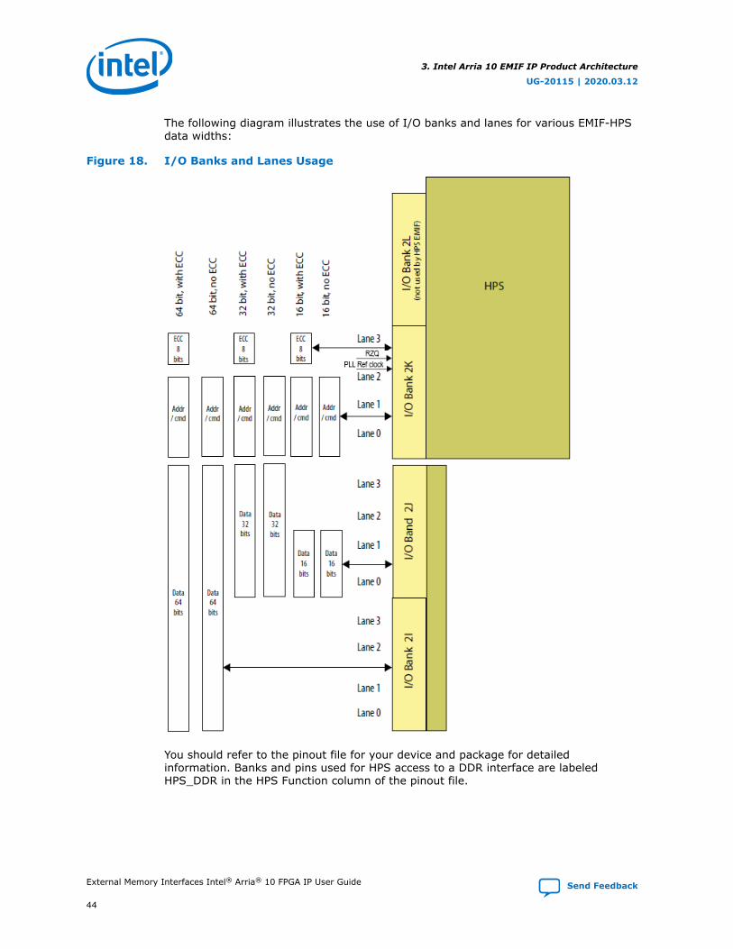
The following diagram illustrates the use of I/O banks and lanes for various EMIF-HPSdata widths:
Figure 18. I/O Banks and Lanes Usage
You should refer to the pinout file for your device and package for detailedinformation. Banks and pins used for HPS access to a DDR interface are labeledHPS_DDR in the HPS Function column of the pinout file.
3. Intel Arria 10 EMIF IP Product Architecture
UG-20115 | 2020.03.12
External Memory Interfaces Intel® Arria® 10 FPGA IP User Guide Send Feedback
By default, the Intel Arria 10 External Memory Interface for HPS IP core together withthe Intel Quartus Prime Fitter automatically implement the correct pin-out for HPSEMIF without you having to implement additional constraints. If, for any reason, youmust modify the default pin-out, you must adhere to the following requirements,which are specific to HPS EMIF:
1. Within a single data lane (which implements a single x8 DQS group):
a. DQ pins must use pins at indices 1, 2, 3, 6, 7, 8, 9, 10. You may swap thelocations between the DQ bits (that is, you may swap location of DQ[0] andDQ[3]) so long as the resulting pin-out uses pins at these indices only.
b. DM/DBI pin must use pin at index 11. There is no flexibility.
c. DQS/DQS# must use pins at index 4 and 5. There is no flexibility.
2. Assignment of data lanes must be as illustrated in the above figure. You areallowed to swap the locations of entire byte lanes (that is, you may swap locationsof byte 0 and byte 3) so long as the resulting pin-out uses only the lanespermitted by your HPS EMIF configuration, as shown in the above figure.
3. You must not change placement of the address and command pins from thedefault.
4. You may place the alert# pin at any available pin location in either a data lane oran address and command lane.
5. The PLL reference clock must be placed in I/O bank 2K with the address andcommand pins.
6. The RZQ pin must be placed in I/O bank 2K with the address and command pins.
Note: Steps 5 and 6 above are applicable to new designs using Intel Quartus Prime softwareversions 19.2 and later, and are required to ensure that all combinations of supportedHPS EMIF IP configurations function correctly in hardware. Failing to follow thesepinout rules can result in Fitter errors. For existing functional pinouts that compilesuccessfully in Intel Quartus Prime software versions earlier than 19.2, where you arenot changing the HPS EMIF configuration but want to migrate your design to latersoftware version, contact Intel for details of a workaround.
To override the default generated pin assignments, comment out the relevantHPS_LOCATION assignments in the .qip file, and add your own location assignments(using set_location_assignment) in the .qsf file.
When the HPS is connected to external SDRAM memory, no other Intel Arria 10External Memory Interface IP instances can be placed in the same I/O column.
3.7.2. Using the EMIF Debug Toolkit with Intel Arria 10 HPS Interfaces
The External Memory Interface Debug Toolkit is not directly compatible with Intel Arria10 HPS interfaces.
To debug your Intel Arria 10 HPS interface using the EMIF Debug Toolkit, you shouldcreate an identically parameterized, non-HPS version of your interface, and apply theEMIF Debug Toolkit to that interface. When you finish debugging this non-HPSinterface, you can then apply any needed changes to your HPS interface, and continueyour design development.
3. Intel Arria 10 EMIF IP Product Architecture
UG-20115 | 2020.03.12
Send Feedback External Memory Interfaces Intel® Arria® 10 FPGA IP User Guide
Ping Pong PHY allows two memory interfaces to share the address and command busthrough time multiplexing. Compared to having two independent interfaces thatallocate address and command lanes separately, Ping Pong PHY achieves the samethroughput with fewer resources, by sharing the address and command lanes.
In Intel Arria 10 EMIF, Ping Pong PHY supports both half-rate and quarter-rateinterfaces for DDR3, and quarter-rate for DDR4.
3.8.1. Ping Pong PHY Feature Description
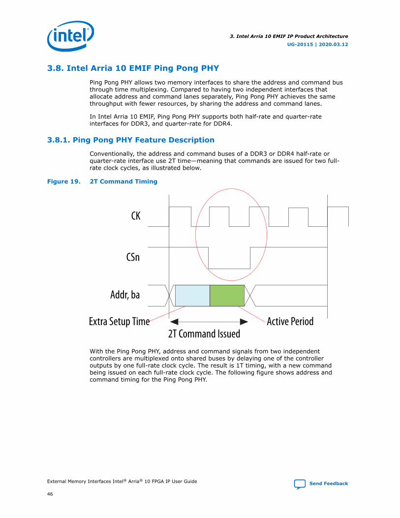
Conventionally, the address and command buses of a DDR3 or DDR4 half-rate orquarter-rate interface use 2T time—meaning that commands are issued for two full-rate clock cycles, as illustrated below.
Figure 19. 2T Command Timing
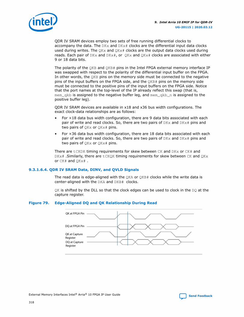
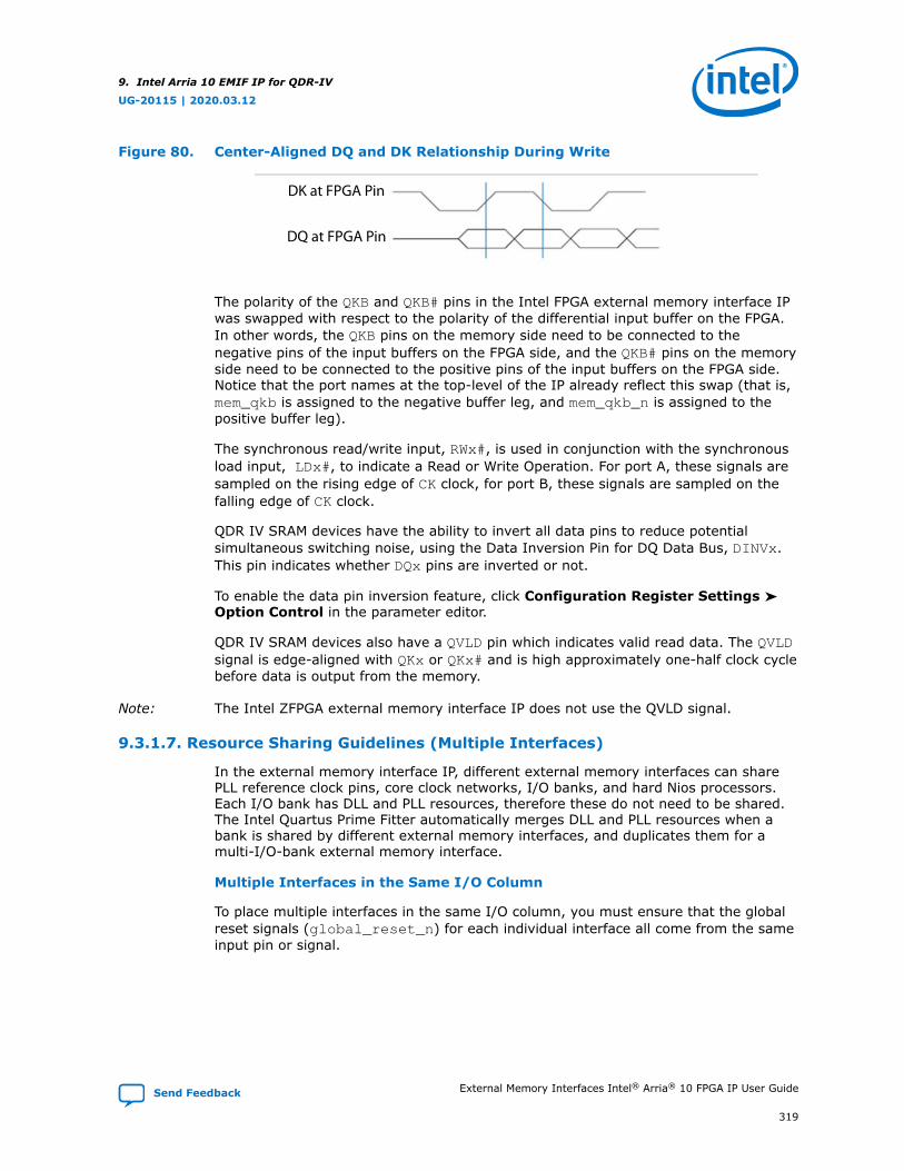
CK
CSn
Addr, ba
2T Command IssuedExtra Setup Time Active Period
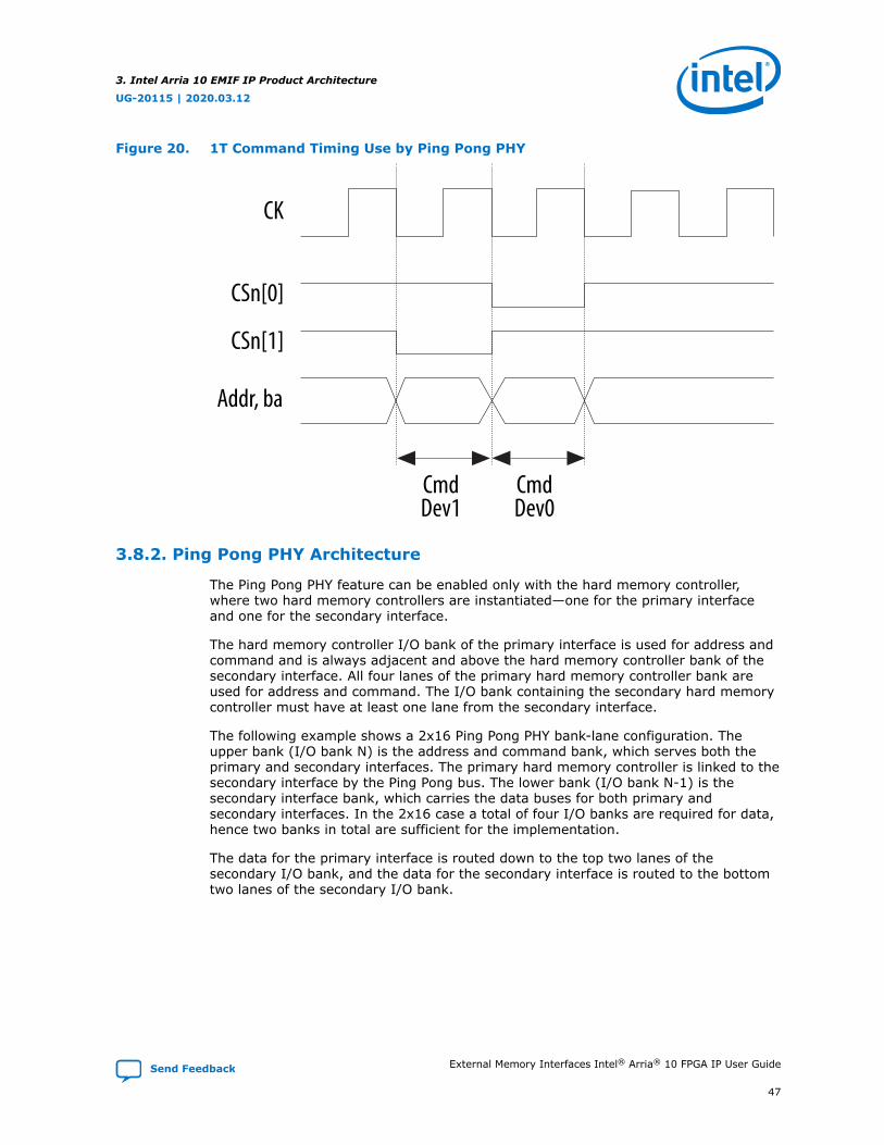
With the Ping Pong PHY, address and command signals from two independentcontrollers are multiplexed onto shared buses by delaying one of the controlleroutputs by one full-rate clock cycle. The result is 1T timing, with a new commandbeing issued on each full-rate clock cycle. The following figure shows address andcommand timing for the Ping Pong PHY.
3. Intel Arria 10 EMIF IP Product Architecture
UG-20115 | 2020.03.12
External Memory Interfaces Intel® Arria® 10 FPGA IP User Guide Send Feedback
The Ping Pong PHY feature can be enabled only with the hard memory controller,where two hard memory controllers are instantiated—one for the primary interfaceand one for the secondary interface.
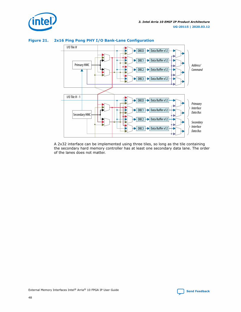
The hard memory controller I/O bank of the primary interface is used for address andcommand and is always adjacent and above the hard memory controller bank of thesecondary interface. All four lanes of the primary hard memory controller bank areused for address and command. The I/O bank containing the secondary hard memorycontroller must have at least one lane from the secondary interface.
The following example shows a 2x16 Ping Pong PHY bank-lane configuration. Theupper bank (I/O bank N) is the address and command bank, which serves both theprimary and secondary interfaces. The primary hard memory controller is linked to thesecondary interface by the Ping Pong bus. The lower bank (I/O bank N-1) is thesecondary interface bank, which carries the data buses for both primary andsecondary interfaces. In the 2x16 case a total of four I/O banks are required for data,hence two banks in total are sufficient for the implementation.
The data for the primary interface is routed down to the top two lanes of thesecondary I/O bank, and the data for the secondary interface is routed to the bottomtwo lanes of the secondary I/O bank.
3. Intel Arria 10 EMIF IP Product Architecture
UG-20115 | 2020.03.12
Send Feedback External Memory Interfaces Intel® Arria® 10 FPGA IP User Guide
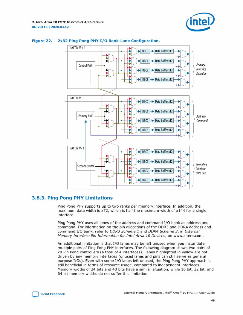
A 2x32 interface can be implemented using three tiles, so long as the tile containingthe secondary hard memory controller has at least one secondary data lane. The orderof the lanes does not matter.
3. Intel Arria 10 EMIF IP Product Architecture
UG-20115 | 2020.03.12
External Memory Interfaces Intel® Arria® 10 FPGA IP User Guide Send Feedback
Ping Pong PHY supports up to two ranks per memory interface. In addition, themaximum data width is x72, which is half the maximum width of x144 for a singleinterface.
Ping Pong PHY uses all lanes of the address and command I/O bank as address andcommand. For information on the pin allocations of the DDR3 and DDR4 address andcommand I/O bank, refer to DDR3 Scheme 1 and DDR4 Scheme 3, in ExternalMemory Interface Pin Information for Intel Arria 10 Devices, on www.altera.com.
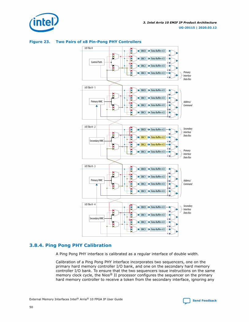
An additional limitation is that I/O lanes may be left unused when you instantiatemultiple pairs of Ping Pong PHY interfaces. The following diagram shows two pairs ofx8 Pin Pong controllers (a total of 4 interfaces). Lanes highlighted in yellow are notdriven by any memory interfaces (unused lanes and pins can still serve as generalpurpose I/Os). Even with some I/O lanes left unused, the Ping Pong PHY approach isstill beneficial in terms of resource usage, compared to independent interfaces.Memory widths of 24 bits and 40 bits have a similar situation, while 16 bit, 32 bit, and64 bit memory widths do not suffer this limitation.
3. Intel Arria 10 EMIF IP Product Architecture
UG-20115 | 2020.03.12
Send Feedback External Memory Interfaces Intel® Arria® 10 FPGA IP User Guide
Figure 23. Two Pairs of x8 Pin-Pong PHY Controllers
Primary HMC
DBCO Data Buffer x12
DBC1 Data Buffer x12
DBC2 Data Buffer x12
DBC3 Data Buffer x12
I/O Tile N - 1
Address/Command
Control Path
DBCO Data Buffer x12
DBC1 Data Buffer x12
DBC2 Data Buffer x12
DBC3 Data Buffer x12
I/O Tile N
PrimaryInterfaceData Bus
Secondary HMC
DBCO Data Buffer x12
DBC1 Data Buffer x12
DBC2 Data Buffer x12
DBC3 Data Buffer x12
I/O Tile N - 4 SecondaryInterfaceData Bus
Primary HMC
DBCO Data Buffer x12
DBC1 Data Buffer x12
DBC2 Data Buffer x12
DBC3 Data Buffer x12
I/O Tile N - 3
Address/Command
Secondary HMC
DBCO Data Buffer x12
DBC1 Data Buffer x12
DBC2 Data Buffer x12
DBC3 Data Buffer x12
I/O Tile N - 2SecondaryInterfaceData Bus
PrimaryInterfaceData Bus
3.8.4. Ping Pong PHY Calibration
A Ping Pong PHY interface is calibrated as a regular interface of double width.
Calibration of a Ping Pong PHY interface incorporates two sequencers, one on theprimary hard memory controller I/O bank, and one on the secondary hard memorycontroller I/O bank. To ensure that the two sequencers issue instructions on the samememory clock cycle, the Nios® II processor configures the sequencer on the primaryhard memory controller to receive a token from the secondary interface, ignoring any
3. Intel Arria 10 EMIF IP Product Architecture
UG-20115 | 2020.03.12
External Memory Interfaces Intel® Arria® 10 FPGA IP User Guide Send Feedback
commands from the Avalon bus. Additional delays are programmed on the secondaryinterface to allow for the passing of the token from the sequencer on the secondaryhard memory controller tile to the sequencer on the primary hard memory controllertile. During calibration, the Nios II processor assumes that commands are alwaysissued from the sequencer on the primary hard memory controller I/O bank. Aftercalibration, the Nios II processor adjusts the delays for use with the primary andsecondary hard memory controllers.
3.8.5. Using the Ping Pong PHY
The following steps describe how to use the Ping Pong PHY for Intel Arria 10 EMIF.
1. Configure a single memory interface according to your requirements.
2. Select Instantiate two controllers sharing a Ping Pong PHY on the Generaltab in the parameter editor.The Intel Quartus Prime software replicates the interface, resulting in two memorycontrollers and a shared PHY. The system configures the I/O bank-lane structure,without further input from you.
3.8.6. Ping Pong PHY Simulation Example Design
The following figure illustrates a top-level block diagram of a generated Ping Pong PHYsimulation example design, using two I/O banks.
Functionally, the IP interfaces with user traffic separately, as it would with twoindependent memory interfaces. You can also generate synthesizable exampledesigns, where the external memory interface IP interfaces with a traffic generator.
Figure 24. Ping Pong PHY Simulation Example Design
Lane 3
Lane 2
Lane 1
Lane 0Primary
HMC
Tile N
Lane 3
Lane 2
Lane 1
Lane 0Secondary
HMC
Tile N - 1
EMIF
TrafficGenerator 0
TrafficGenerator 1
SimChecker
Memory0
Memory1
CS, ODT, CKE
CAS, RAS, WE, ADDR, BA, BG, ...
CS, ODT, CKE
DQ, DQS, DM
DQ, DQS, DM
Simulation Example Design
3.9. Intel Arria 10 EMIF and SmartVID
The external memory interface IP can work with the SmartVID voltage managementsystem, to achieve reduced power consumption.
3. Intel Arria 10 EMIF IP Product Architecture
UG-20115 | 2020.03.12
Send Feedback External Memory Interfaces Intel® Arria® 10 FPGA IP User Guide
Note: Intel Arria 10 HPS EMIF IP does not currently support SmartVID.
The SmartVID controller allows the FPGA to operate at a reduced Vcc, whilemaintaining performance. Because the SmartVID controller can adjust Vcc up or downin response to power requirements and temperature, it can have an impact onexternal memory interface performance. When used with the SmartVID controller, theEMIF IP implements a handshake protocol to ensure that EMIF calibration does notbegin until after voltage adjustment has completed.
In extended speed grade devices, voltage adjustment occurs once when the FPGA ispowered up, and no further voltage adjustments occur. The external memorycalibration occurs after this initial voltage adjustment is completed. EMIF specificationsare expected to be slightly lower in extended speed grade devices using SmartVID,than in devices not using SmartVID.
In industrial speed grade devices, voltage adjustment occurs at power up, and mayalso occur during operation, in response to temperature changes. External memoryinterface calibration does not occur until after the initial voltage adjustment at powerup. However, the external memory interface is not recalibrated in response tosubsequent voltage adjustments that occur during operation. As a result, EMIFspecifications for industrial speed grade devices using SmartVID are expected to belower than for extended speed grade devices.
Using the EMIF IP with SmartVID
To use your EMIF IP with SmartVID, follow these steps:
1. Ensure that the Intel Quartus Prime project and Platform Designer system areconfigured to use VID components. This step exposes thevid_cal_done_persist interface on instantiated EMIF IP, which is required forcommunicating with the SmartVID controller.
2. Instantiate the SmartVID controller, using an I/O PLL IP core to drive the 125MHzvid_clk and the 25MHz jtag_core_clk inputs of the Smart VID controller.
Note: Do not connect the emif_usr_clk signal to either the vid_clk orjtag_core_clk inputs. Doing so would hold both the EMIF IP and theSmartVID controller in a perpetual reset condition.
3. Instantiate the EMIF IP.
4. Connect the vid_cal_done_persist signal from the EMIF IP with thecal_done_persistent signal on the SmartVID controller. This connectionenables handshaking between the EMIF IP and the SmartVID controller, whichallows the EMIF IP to delay memory calibration until after voltage levels arestabilized.
Note: The EMIF vid_cal_done_persist interface becomes available only whena VID-enabled device is selected.
3. Intel Arria 10 EMIF IP Product Architecture
UG-20115 | 2020.03.12
External Memory Interfaces Intel® Arria® 10 FPGA IP User Guide Send Feedback
The following sections describe each of the interfaces and their signals, by protocol,for the Intel Arria 10 EMIF IP.
4.1.1. Intel Arria 10 EMIF IP Interfaces for DDR3
The interfaces in the Intel Arria 10 External Memory Interface IP each have signalsthat can be connected in Qsys. The following table lists the interfaces andcorresponding interface types for DDR3.
emif_usr_reset_n Reset Output User clock domain reset interface
emif_usr_clk Clock Output User clock interface
emif_usr_reset_n_sec Reset Output User clock domain reset interface (for the secondaryinterface in ping-pong configuration)
continued...
UG-20115 | 2020.03.12
Send Feedback
Intel Corporation. All rights reserved. Agilex, Altera, Arria, Cyclone, Enpirion, Intel, the Intel logo, MAX, Nios,Quartus and Stratix words and logos are trademarks of Intel Corporation or its subsidiaries in the U.S. and/orother countries. Intel warrants performance of its FPGA and semiconductor products to current specifications inaccordance with Intel's standard warranty, but reserves the right to make changes to any products and servicesat any time without notice. Intel assumes no responsibility or liability arising out of the application or use of anyinformation, product, or service described herein except as expressly agreed to in writing by Intel. Intelcustomers are advised to obtain the latest version of device specifications before relying on any publishedinformation and before placing orders for products or services.*Other names and brands may be claimed as the property of others.
pll_extra_clk_0 Output PLL extra core clock signal output 0. This signal exists if youspecify the EMIF PLL to generate additional output clocksignals (up to 4) that can be used by user logic. This clocksignal is asynchronous to the memory interface core clockdomains (such as emif_usr_clk or afi_clk). You must followproper clock-domain-crossing techniques when transferringdata between clock domains.
pll_extra_clk_1 Output PLL extra core clock signal output 1. This signal exists if youspecify the EMIF PLL to generate additional output clocksignals (up to 4) that can be used by user logic. This clocksignal is asynchronous to the memory interface core clockdomains (such as emif_usr_clk or afi_clk). You must followproper clock-domain-crossing techniques when transferringdata between clock domains.
pll_extra_clk_2 Output PLL extra core clock signal output 2. This signal exists if youspecify the EMIF PLL to generate additional output clocksignals (up to 4) that can be used by user logic. This clocksignal is asynchronous to the memory interface core clockdomains (such as emif_usr_clk or afi_clk). You must followproper clock-domain-crossing techniques when transferringdata between clock domains.
pll_extra_clk_3 Output PLL extra core clock signal output 3. This signal exists if youspecify the EMIF PLL to generate additional output clocksignals (up to 4) that can be used by user logic. This clock
4. Intel Arria 10 EMIF IP End-User Signals
UG-20115 | 2020.03.12
Send Feedback External Memory Interfaces Intel® Arria® 10 FPGA IP User Guide
signal is asynchronous to the memory interface core clockdomains (such as emif_usr_clk or afi_clk). You must followproper clock-domain-crossing techniques when transferringdata between clock domains.
emif_usr_reset_n_sec Output Reset for the user clock domain. Asynchronous assertionand synchronous deassertion. Intended for the secondaryinterface in a ping-pong configuration.
4.1.1.17. emif_usr_clk_sec for DDR3
User clock interface (for the secondary interface in ping-pong configuration)
cal_debug_out_reset_n Output Reset for the user clock connecting to the Avalon calibrationdebug_out bus. Asynchronous assertion and synchronousdeassertion
ctrl_auto_precharge_req Input When asserted high along with a read or write request tothe memory controller, indicates that the controller shouldclose the currently opened page after the read or writeburst.
ctrl_user_priority_hi Input When asserted high along with a read or write request tothe memory controller, indicates that the request is highpriority and should be fullfilled before other low priorityrequests.
ctrl_ecc_readdataerror Output Signal is asserted high by the controller ECC logic toindicate that the read data has an uncorrectable error. Thesignal has the same timing as the read data valid signal ofthe Controller Avalon Memory-Mapped interface.
4.1.1.30. ctrl_mmr_slave for DDR3
Controller MMR slave interface
4. Intel Arria 10 EMIF IP End-User Signals
UG-20115 | 2020.03.12
External Memory Interfaces Intel® Arria® 10 FPGA IP User Guide Send Feedback
cal_debug_out_waitrequest Input Wait-request is asserted when controller is busy
cal_debug_out_read Output Read request signal
cal_debug_out_write Output Write request signal
cal_debug_out_addr Output Address for the read/write request
cal_debug_out_read_data Input Read data
cal_debug_out_write_data Output Write data
cal_debug_out_byteenable Output Byte-enable for write data
cal_debug_out_read_data_valid Input Indicates whether read data is valid
4.1.2. Intel Arria 10 EMIF IP Interfaces for DDR4
The interfaces in the Intel Arria 10 External Memory Interface IP each have signalsthat can be connected in Qsys. The following table lists the interfaces andcorresponding interface types for DDR4.
pll_extra_clk_0 Output PLL extra core clock signal output 0. This signal exists if youspecify the EMIF PLL to generate additional output clocksignals (up to 4) that can be used by user logic. This clocksignal is asynchronous to the memory interface core clockdomains (such as emif_usr_clk or afi_clk). You must followproper clock-domain-crossing techniques when transferringdata between clock domains.
pll_extra_clk_1 Output PLL extra core clock signal output 1. This signal exists if youspecify the EMIF PLL to generate additional output clocksignals (up to 4) that can be used by user logic. This clocksignal is asynchronous to the memory interface core clockdomains (such as emif_usr_clk or afi_clk). You must followproper clock-domain-crossing techniques when transferringdata between clock domains.
pll_extra_clk_2 Output PLL extra core clock signal output 2. This signal exists if youspecify the EMIF PLL to generate additional output clocksignals (up to 4) that can be used by user logic. This clocksignal is asynchronous to the memory interface core clockdomains (such as emif_usr_clk or afi_clk). You must followproper clock-domain-crossing techniques when transferringdata between clock domains.
4. Intel Arria 10 EMIF IP End-User Signals
UG-20115 | 2020.03.12
External Memory Interfaces Intel® Arria® 10 FPGA IP User Guide Send Feedback
pll_extra_clk_3 Output PLL extra core clock signal output 3. This signal exists if youspecify the EMIF PLL to generate additional output clocksignals (up to 4) that can be used by user logic. This clocksignal is asynchronous to the memory interface core clockdomains (such as emif_usr_clk or afi_clk). You must followproper clock-domain-crossing techniques when transferringdata between clock domains.
emif_usr_reset_n_sec Output Reset for the user clock domain. Asynchronous assertionand synchronous deassertion. Intended for the secondaryinterface in a ping-pong configuration.
4.1.2.17. emif_usr_clk_sec for DDR4
User clock interface (for the secondary interface in ping-pong configuration)
cal_debug_out_reset_n Output Reset for the user clock connecting to the Avalon calibrationdebug_out bus. Asynchronous assertion and synchronousdeassertion
ctrl_auto_precharge_req Input When asserted high along with a read or write request tothe memory controller, indicates that the controller shouldclose the currently opened page after the read or writeburst.
ctrl_user_priority_hi Input When asserted high along with a read or write request tothe memory controller, indicates that the request is highpriority and should be fullfilled before other low priorityrequests.
ctrl_ecc_readdataerror Output Signal is asserted high by the controller ECC logic toindicate that the read data has an uncorrectable error. Thesignal has the same timing as the read data valid signal ofthe Controller Avalon Memory-Mapped interface.
4.1.2.30. ctrl_mmr_slave for DDR4
Controller MMR slave interface
4. Intel Arria 10 EMIF IP End-User Signals
UG-20115 | 2020.03.12
Send Feedback External Memory Interfaces Intel® Arria® 10 FPGA IP User Guide
cal_debug_out_waitrequest Input Wait-request is asserted when controller is busy
cal_debug_out_read Output Read request signal
cal_debug_out_write Output Write request signal
cal_debug_out_addr Output Address for the read/write request
cal_debug_out_read_data Input Read data
cal_debug_out_write_data Output Write data
cal_debug_out_byteenable Output Byte-enable for write data
cal_debug_out_read_data_valid Input Indicates whether read data is valid
4.1.3. Intel Arria 10 EMIF IP Interfaces for LPDDR3
The interfaces in the Intel Arria 10 External Memory Interface IP each have signalsthat can be connected in Qsys. The following table lists the interfaces andcorresponding interface types for LPDDR3.
pll_extra_clk_0 Output PLL extra core clock signal output 0. This signal exists if youspecify the EMIF PLL to generate additional output clocksignals (up to 4) that can be used by user logic. This clocksignal is asynchronous to the memory interface core clockdomains (such as emif_usr_clk or afi_clk). You must followproper clock-domain-crossing techniques when transferringdata between clock domains.
pll_extra_clk_1 Output PLL extra core clock signal output 1. This signal exists if youspecify the EMIF PLL to generate additional output clocksignals (up to 4) that can be used by user logic. This clocksignal is asynchronous to the memory interface core clockdomains (such as emif_usr_clk or afi_clk). You must followproper clock-domain-crossing techniques when transferringdata between clock domains.
pll_extra_clk_2 Output PLL extra core clock signal output 2. This signal exists if youspecify the EMIF PLL to generate additional output clocksignals (up to 4) that can be used by user logic. This clocksignal is asynchronous to the memory interface core clockdomains (such as emif_usr_clk or afi_clk). You must followproper clock-domain-crossing techniques when transferringdata between clock domains.
pll_extra_clk_3 Output PLL extra core clock signal output 3. This signal exists if youspecify the EMIF PLL to generate additional output clocksignals (up to 4) that can be used by user logic. This clocksignal is asynchronous to the memory interface core clock
4. Intel Arria 10 EMIF IP End-User Signals
UG-20115 | 2020.03.12
Send Feedback External Memory Interfaces Intel® Arria® 10 FPGA IP User Guide
cal_debug_out_reset_n Output Reset for the user clock connecting to the Avalon calibrationdebug_out bus. Asynchronous assertion and synchronousdeassertion
ctrl_user_priority_hi Input When asserted high along with a read or write request tothe memory controller, indicates that the request is highpriority and should be fullfilled before other low priorityrequests.
4.1.4. Intel Arria 10 EMIF IP Interfaces for QDR II/II+/II+ Xtreme
The interfaces in the Intel Arria 10 External Memory Interface IP each have signalsthat can be connected in Qsys. The following table lists the interfaces andcorresponding interface types for QDR II/II+/II+ Xtreme.
pll_extra_clk_0 Output PLL extra core clock signal output 0. This signal exists if youspecify the EMIF PLL to generate additional output clocksignals (up to 4) that can be used by user logic. This clocksignal is asynchronous to the memory interface core clockdomains (such as emif_usr_clk or afi_clk). You must followproper clock-domain-crossing techniques when transferringdata between clock domains.
4.1.4.4. pll_extra_clk_1 for QDR II/II+/II+ Xtreme
pll_extra_clk_1 Output PLL extra core clock signal output 1. This signal exists if youspecify the EMIF PLL to generate additional output clocksignals (up to 4) that can be used by user logic. This clocksignal is asynchronous to the memory interface core clockdomains (such as emif_usr_clk or afi_clk). You must followproper clock-domain-crossing techniques when transferringdata between clock domains.
4.1.4.5. pll_extra_clk_2 for QDR II/II+/II+ Xtreme
pll_extra_clk_2 Output PLL extra core clock signal output 2. This signal exists if youspecify the EMIF PLL to generate additional output clocksignals (up to 4) that can be used by user logic. This clocksignal is asynchronous to the memory interface core clock
4. Intel Arria 10 EMIF IP End-User Signals
UG-20115 | 2020.03.12
Send Feedback External Memory Interfaces Intel® Arria® 10 FPGA IP User Guide
pll_extra_clk_3 Output PLL extra core clock signal output 3. This signal exists if youspecify the EMIF PLL to generate additional output clocksignals (up to 4) that can be used by user logic. This clocksignal is asynchronous to the memory interface core clockdomains (such as emif_usr_clk or afi_clk). You must followproper clock-domain-crossing techniques when transferringdata between clock domains.
cal_debug_out_reset_n Output Reset for the user clock connecting to the Avalon calibrationdebug_out bus. Asynchronous assertion and synchronousdeassertion
4.1.4.15. cal_debug_out_clk for QDR II/II+/II+ Xtreme
cal_debug_out_waitrequest Input Wait-request is asserted when controller is busy
cal_debug_out_read Output Read request signal
cal_debug_out_write Output Write request signal
cal_debug_out_addr Output Address for the read/write request
cal_debug_out_read_data Input Read data
cal_debug_out_write_data Output Write data
cal_debug_out_byteenable Output Byte-enable for write data
cal_debug_out_read_data_valid Input Indicates whether read data is valid
4.1.5. Intel Arria 10 EMIF IP Interfaces for QDR-IV
The interfaces in the Intel Arria 10 External Memory Interface IP each have signalsthat can be connected in Qsys. The following table lists the interfaces andcorresponding interface types for QDR-IV.
pll_extra_clk_0 Output PLL extra core clock signal output 0. This signal exists if youspecify the EMIF PLL to generate additional output clocksignals (up to 4) that can be used by user logic. This clocksignal is asynchronous to the memory interface core clockdomains (such as emif_usr_clk or afi_clk). You must followproper clock-domain-crossing techniques when transferringdata between clock domains.
pll_extra_clk_1 Output PLL extra core clock signal output 1. This signal exists if youspecify the EMIF PLL to generate additional output clocksignals (up to 4) that can be used by user logic. This clocksignal is asynchronous to the memory interface core clockdomains (such as emif_usr_clk or afi_clk). You must followproper clock-domain-crossing techniques when transferringdata between clock domains.
pll_extra_clk_2 Output PLL extra core clock signal output 2. This signal exists if youspecify the EMIF PLL to generate additional output clocksignals (up to 4) that can be used by user logic. This clocksignal is asynchronous to the memory interface core clockdomains (such as emif_usr_clk or afi_clk). You must followproper clock-domain-crossing techniques when transferringdata between clock domains.
4. Intel Arria 10 EMIF IP End-User Signals
UG-20115 | 2020.03.12
External Memory Interfaces Intel® Arria® 10 FPGA IP User Guide Send Feedback
pll_extra_clk_3 Output PLL extra core clock signal output 3. This signal exists if youspecify the EMIF PLL to generate additional output clocksignals (up to 4) that can be used by user logic. This clocksignal is asynchronous to the memory interface core clockdomains (such as emif_usr_clk or afi_clk). You must followproper clock-domain-crossing techniques when transferringdata between clock domains.
cal_debug_out_reset_n Output Reset for the user clock connecting to the Avalon calibrationdebug_out bus. Asynchronous assertion and synchronousdeassertion
4.1.5.19. cal_debug_out_clk for QDR-IV
User calibration debug clock interface
4. Intel Arria 10 EMIF IP End-User Signals
UG-20115 | 2020.03.12
External Memory Interfaces Intel® Arria® 10 FPGA IP User Guide Send Feedback
4.1.6. Intel Arria 10 EMIF IP Interfaces for RLDRAM 3
The interfaces in the Intel Arria 10 External Memory Interface IP each have signalsthat can be connected in Qsys. The following table lists the interfaces andcorresponding interface types for RLDRAM 3.
pll_extra_clk_0 Output PLL extra core clock signal output 0. This signal exists if youspecify the EMIF PLL to generate additional output clocksignals (up to 4) that can be used by user logic. This clocksignal is asynchronous to the memory interface core clockdomains (such as emif_usr_clk or afi_clk). You must followproper clock-domain-crossing techniques when transferringdata between clock domains.
pll_extra_clk_1 Output PLL extra core clock signal output 1. This signal exists if youspecify the EMIF PLL to generate additional output clocksignals (up to 4) that can be used by user logic. This clocksignal is asynchronous to the memory interface core clockdomains (such as emif_usr_clk or afi_clk). You must followproper clock-domain-crossing techniques when transferringdata between clock domains.
pll_extra_clk_2 Output PLL extra core clock signal output 2. This signal exists if youspecify the EMIF PLL to generate additional output clocksignals (up to 4) that can be used by user logic. This clocksignal is asynchronous to the memory interface core clock
4. Intel Arria 10 EMIF IP End-User Signals
UG-20115 | 2020.03.12
External Memory Interfaces Intel® Arria® 10 FPGA IP User Guide Send Feedback
pll_extra_clk_3 Output PLL extra core clock signal output 3. This signal exists if youspecify the EMIF PLL to generate additional output clocksignals (up to 4) that can be used by user logic. This clocksignal is asynchronous to the memory interface core clockdomains (such as emif_usr_clk or afi_clk). You must followproper clock-domain-crossing techniques when transferringdata between clock domains.
cal_debug_out_reset_n Output Reset for the user clock connecting to the Avalon calibrationdebug_out bus. Asynchronous assertion and synchronousdeassertion
cal_debug_out_waitrequest Input Wait-request is asserted when controller is busy
cal_debug_out_read Output Read request signal
cal_debug_out_write Output Write request signal
cal_debug_out_addr Output Address for the read/write request
cal_debug_out_read_data Input Read data
cal_debug_out_write_data Output Write data
cal_debug_out_byteenable Output Byte-enable for write data
cal_debug_out_read_data_valid Input Indicates whether read data is valid
4.2. AFI Signals
The following tables list Altera PHY interface (AFI) signals grouped according to theirfunctions.
In each table, the Direction column denotes the direction of the signal relative to thePHY. For example, a signal defined as an output passes out of the PHY to thecontroller. The AFI specification does not include any bidirectional signals.
Note: Not all signals listed apply to every device family or every memory protocol.
4.2.1. AFI Clock and Reset Signals
The AFI interface provides up to two clock signals and an asynchronous reset signal.
Table 174. Clock and Reset Signals
Signal Name Direction Width Description
afi_clk Output 1 Clock with which all data exchanged on the AFI busis synchronized. In general, this clock is referred toas full-rate, half-rate, or quarter-rate, depending onthe ratio between the frequency of this clock andthe frequency of the memory device clock.
afi_half_clk Output 1 Clock signal that runs at half the speed of theafi_clk. The controller uses this signal when thehalf-rate bridge feature is in use. This signal isoptional.
afi_reset_n Output 1 Asynchronous reset output signal. You mustsynchronize this signal to the clock domain in whichyou use it.
4.2.2. AFI Address and Command Signals
The address and command signals for AFI 4.0 encode read/write/configurationcommands to send to the memory device. The address and command signals aresingle-data rate signals.
4. Intel Arria 10 EMIF IP End-User Signals
UG-20115 | 2020.03.12
External Memory Interfaces Intel® Arria® 10 FPGA IP User Guide Send Feedback
afi_addr Input AFI_ADDR_WIDTH Address or CA bus (LPDDR3 only).ADDR_RATE_RATIO is 2 forLPDDR3 CA bus.
afi_bg Input AFI_BANKGROUP_WIDTH Bank group (DDR4 only).
afi_ba Input AFI_BANKADDR_WIDTH Bank address. (Not applicable forLPDDR3.)
afi_cke Input AFI_CLK_EN_WIDTH Clock enable.
afi_cs_n Input AFI_CS_WIDTH Chip select signal. (The number ofchip selects may not match thenumber of ranks; for example,RDIMMs and LRDIMMs require aminimum of 2 chip select signalsfor both single-rank and dual-rankconfigurations. Consult yourmemory device data sheet forinformation about chip select signalwidth.) (Matches the number ofranks for LPDDR3.)
afi_rst_n Input AFI_CONTROL_WIDTH RESET# (for DDR3 and DDR4memory devices.)
afi_odt Input AFI_CLK_EN_WIDTH On-die termination signal for DDR3,and LPDDR3 memory devices. (Donot confuse this memory devicesignal with the FPGA’s internal on-chip termination signal.)
afi_dqs_burst Input AFI_RATE_RATIO Controls the enable on the strobe(DQS) pins for DDR3 and LPDDR3memory devices. When this signalis asserted, mem_dqs andmem_dqsn are driven.This signal must be asserted beforeafi_wdata_valid to implement thewrite preamble, and must be drivenfor the correct duration to generatea correctly timed mem_dqs signal.
afi_wdata_valid Input AFI_RATE_RATIO Write data valid signal. This signalcontrols the output enable on thedata and data mask pins.
afi_wdata Input AFI_DQ_WIDTH Write data signal to send to thememory device at double-datarate. This signal controls the PHY’smem_dq output.
afi_dm Input AFI_DM_WIDTH Data mask. This signal controls thePHY’s mem_dm signal for DDR3and LPDDR3 memory devices.Also directly controls the PHY'smem_dbi signal for DDR4.The mem_dm and mem_dbifeatures share the same port onthe memory device.
afi_bws_n Input AFI_DM_WIDTH Data mask. This signal controls thePHY’s mem_bws_n signal forQDR II/II+ memory devices.
afi_dinv Input AFI_WRITE_DQS_WIDTH * 2 Data inversion. It directly controlsthe PHY's mem_dinva/b signal forQDR-IV devices.
4.2.4. AFI Read Data Signals
Read Data Signals for AFI 4.0 control the data sent from the memory device duringread operations.
Table 177. Read Data Signals
Signal Name Direction Width Description
afi_rdata_en_full Input AFI_RATE_RATIO Read data enable full. Indicates that thememory controller is currently performinga read operation. This signal is held highfor the entire read burst.If this signal isaligned to even clock cycles, it is possibleto use 1-bit even in half-rate mode (i.e.,AFI_RATE=2).
afi_rdata Output AFI_DQ_WIDTH Read data from the memory device. Thisdata is considered valid only whenafi_rdata_valid is asserted by the PHY.
afi_rdata_valid Output AFI_RATE_RATIO Read data valid. When asserted, thissignal indicates that the afi_rdata bus isvalid.If this signal is aligned to even clockcycles, it is possible to use 1-bit even inhalf-rate mode (i.e., AFI_RATE=2).
4. Intel Arria 10 EMIF IP End-User Signals
UG-20115 | 2020.03.12
External Memory Interfaces Intel® Arria® 10 FPGA IP User Guide Send Feedback
The PHY instantiates a sequencer which calibrates the memory interface with thememory device and some internal components such as read FIFOs and valid FIFOs.The sequencer reports the results of the calibration process to the controller throughthe Calibration Status Signals in the AFI interface.
Table 178. Calibration Status Signals
Signal Name Direction Width Description
afi_cal_success Output 1 Asserted to indicate that calibration hascompleted successfully.
afi_cal_fail Output 1 Asserted to indicate that calibration hasfailed.
afi_cal_req Input 1 Effectively a synchronous reset for thesequencer. When this signal is asserted,the sequencer returns to the reset state;when this signal is released, a newcalibration sequence begins.
afi_wlat Output AFI_WLAT_WIDTH The required write latency in afi_clkcycles, between address/command andwrite data being issued at the PHY/controller interface. The afi_wlat valuecan be different for different groups; eachgroup’s write latency can range from 0 to63. If write latency is the same for allgroups, only the lowest 6 bits arerequired.
afi_rlat(1)
Output AFI_RLAT_WIDTH The required read latency in afi_clk cyclesbetween address/command and readdata being returned to the PHY/controllerinterface. Values can range from 0 to 63.
Note to Table:1. The afi_rlat signal is not supported for PHY-only designs. Instead, you can sample the afi_rdata_valid signal to
determine when valid read data is available.
4.2.6. AFI Tracking Management Signals
When tracking management is enabled, the sequencer can take control over the AFI4.0 interface at given intervals, and issue commands to the memory device to trackthe internal DQS Enable signal alignment to the DQS signal returning from thememory device. The tracking management portion of the AFI 4.0 interface provides ameans for the sequencer and the controller to exchange handshake signals.
4. Intel Arria 10 EMIF IP End-User Signals
UG-20115 | 2020.03.12
Send Feedback External Memory Interfaces Intel® Arria® 10 FPGA IP User Guide
afi_ctl_refresh_done Input 4 Handshaking signal from controller totracking manager, indicating that arefresh has occurred and waiting for aresponse.
afi_seq_busy Output 4 Handshaking signal from sequencer tocontroller, indicating when DQS trackingis in progress.
afi_ctl_long_idle Input 4 Handshaking signal from controller totracking manager, indicating that it hasexited low power state without a periodicrefresh, and waiting for response.
4.2.7. AFI Shadow Register Management Signals
Shadow registers are a feature that enables high-speed multi-rank support. Shadowregisters allow the sequencer to calibrate each rank separately, and save thecalibrated settings—such as deskew delay-chain configurations—of each rank in itsown set of shadow registers.
During a rank-to-rank switch, the correct set of calibrated settings is restored just intime to optimize the data valid window. The PHY relies on additional AFI signals tocontrol which set of shadow registers to activate.
Table 180. Shadow Register Management Signals
Signal Name Direction Width Description
afi_wrank Input AFI_WRANK_WIDTH Signal from controllerspecifying which rank thewrite data is going to. Thesignal timing is identical tothat of afi_dqs_burst. Thatis, afi_wrank must beasserted at the same timeand must last the sameduration as theafi_dqs_burst signal.
afi_rrank Output AFI_RRANK_WIDTH Signal from controllerspecifying which rank isbeing read. The signal mustbe asserted at the sametime as the afi_rdata_ensignal when issuing a readcommand, but unlikeafi_rdata_en, afi_rrank isstateful. That is, onceasserted, the signal valuemust remain unchangeduntil the controller issues anew read command to adifferent rank.
4. Intel Arria 10 EMIF IP End-User Signals
UG-20115 | 2020.03.12
External Memory Interfaces Intel® Arria® 10 FPGA IP User Guide Send Feedback
Both the afi_wrank and afi_rrank signals encode the rank being accessed using theone-hot scheme (e.g. in a quad-rank interface, 0001, 0010, 0100, 1000 refer to the1st, 2nd, 3rd, 4th rank respectively). The ordering within the bus is the same as otherAFI signals. Specifically the bus is ordered by time slots, for example:
Half-rate afi_w/rrank = T1, T0
Quarter-rate afi_w/rrank = T3, T2, T1, T0
Where Tx is a number of rank-bit words that one-hot encodes the rank being accessedat the yth full-rate cycle.
Additional Requirements for Shadow Register Support
To ensure that the hardware has enough time to switch from one shadow register toanother, the controller must satisfy the following minimum rank-to-rank-switch delays(tRTRS):
• Two read commands going to different ranks must be separated by a minimum of3 full-rate cycles (in addition to the burst length delay needed to avoid collision ofdata bursts).
• Two write commands going to different rank must be separated by a minimum of4 full-rate cycles (in addition to the burst length delay needed to avoid collision ofdata bursts).
The FPGA device supports a maximum of 4 sets of shadow registers, each for anindependent set of timings. More than 4 ranks are supported if those ranks have fouror fewer sets of independent timing. For example, the rank multiplication mode of anLRDIMM allows more than one physical rank to share a set of timing data as a singlelogical rank. Therefore the device can support up to 4 logical ranks, though thatmeans more than 4 physical ranks.
4.3. AFI 4.0 Timing Diagrams
4.3.1. AFI Address and Command Timing Diagrams
Depending on the ratio between the memory clock and the PHY clock, differentnumbers of bits must be provided per PHY clock on the AFI interface. The followingfigures illustrate the AFI address/command waveforms in full, half and quarter raterespectively.
The waveforms show how the AFI command phase corresponds to the memorycommand output. AFI command 0 corresponds to the first memory command slot, AFIcommand 1 corresponds to the second memory command slot, and so on.
4. Intel Arria 10 EMIF IP End-User Signals
UG-20115 | 2020.03.12
Send Feedback External Memory Interfaces Intel® Arria® 10 FPGA IP User Guide
The following timing diagrams illustrate the relationships between the write commandand corresponding write data and write enable signals, in full, half, and quarter rate.
For half rate and quarter rate, when the write command is sent on the first memoryclock in a PHY clock (for example, afi_cs_n[0] = 0), that access is called alignedaccess; otherwise it is called unaligned access. You may use either aligned orunaligned access, or you may use both, but you must ensure that the distance
4. Intel Arria 10 EMIF IP End-User Signals
UG-20115 | 2020.03.12
External Memory Interfaces Intel® Arria® 10 FPGA IP User Guide Send Feedback
between the write command and the corresponding write data are constant on theAFI interface. For example, if a command is sent on the second memory clock in a PHYclock, the write data must also start at the second memory clock in a PHY clock.
Write sequences with wlat=0
Figure 28. AFI Write Data Full-Rate, wlat=0
WR WR WR
A B C D E F
M N O P Q R
afi_clk
afi_command
afi_wdata_valid
afi_wdata
afi_dm
The following diagrams illustrate both aligned and unaligned access. The first threewrite commands are aligned accesses where they were issued on LSB ofafi_command. The fourth write command is unaligned access where it was issued ona different command slot. AFI signals must be shifted accordingly, based on thecommand slot.
Figure 29. AFI Write Data Half-Rate, wlat=0
NOP NOP NOP
afi_clk
afi_command[1]
WR WR WRafi_command[0]
NOP
WR
1 1 1afi_wdata_valid[1]
1 1 0afi_wdata_valid[0]
1
1
0
1
B D Gafi_wdata[1]
A Cafi_wdata[0]
F
E H
N P Safi_dm[1]
M Oafi_dm[0]
R
Q T
4. Intel Arria 10 EMIF IP End-User Signals
UG-20115 | 2020.03.12
Send Feedback External Memory Interfaces Intel® Arria® 10 FPGA IP User Guide
The afi_wlat is a signal from the PHY. The controller must delay afi_dqs_burst,afi_wdata_valid, afi_wdata and afi_dm signals by a number of PHY clock cyclesequal to afi_wlat, which is a static value determined by calibration before the PHYasserts cal_success to the controller. The following figures illustrate the cases whenwlat=1. Note that wlat is in the number of PHY clocks and therefore wlat=1 equals 1,2, and 4 memory clocks delay, respectively, on full, half and quarter rate.
4. Intel Arria 10 EMIF IP End-User Signals
UG-20115 | 2020.03.12
External Memory Interfaces Intel® Arria® 10 FPGA IP User Guide Send Feedback
The afi_dqs_burst signal must be asserted one or two complete memory clockcycles earlier to generate DQS preamble. DQS preamble is equal to one-half and one-quarter AFI clock cycles in half and quarter rate, respectively.
A DQS preamble of two is required in DDR4, when the write preamble is set to twoclock cycles.
The following diagrams illustrate how afi_dqs_burst must be asserted in full, half, andquarter-rate configurations.
4. Intel Arria 10 EMIF IP End-User Signals
UG-20115 | 2020.03.12
External Memory Interfaces Intel® Arria® 10 FPGA IP User Guide Send Feedback
Write data sequence with DBI (DDR4 and QDRIV only)
The DDR4 write DBI feature is supported in the PHY, and when it is enabled, the PHYsends and receives the DBI signal without any controller involvement. The sequence isidentical to non-DBI scenarios on the AFI interface.
4. Intel Arria 10 EMIF IP End-User Signals
UG-20115 | 2020.03.12
External Memory Interfaces Intel® Arria® 10 FPGA IP User Guide Send Feedback
When the CRC feature of the PHY is enabled and used, the controller ensures at leastone memory clock cycle between write commands, during which the PHY inserts theCRC data. Sending back to back write command would cause functional failure. Thefollowing figures show the legal sequences in CRC mode.
Entries marked as 0 and RESERVE must be observed by the controller; no informationis allowed on those entries.
Figure 37. AFI Write Data with CRC Half-Rate, wlat=2
NOP NOP NOP
afi_clk
afi_command[1]
WR WR WRafi_command[0]
1 1 1afi_wdata_valid[1]
1 1 0afi_wdata_valid[0]
1
1
0
1
B D
G
afi_wdata[1]
A Cafi_wdata[0]
F
E
H
N Pafi_dm[1]
M Oafi_dm[0]
afi_dqs_burst[1]
afi_dqs_burst[0]
1
0
1
1 0
1
1
1
1
1
1
0
1
1
0
1
0
1
1
0
1
1
1
1
Reserve
Reserve
Reserve
Reserve
J
HI
L
S
R
Q
T
Reserve
Reserve
V
WU
X
4. Intel Arria 10 EMIF IP End-User Signals
UG-20115 | 2020.03.12
Send Feedback External Memory Interfaces Intel® Arria® 10 FPGA IP User Guide
Figure 38. AFI Write Data with CRC Quarter-Rate, wlat=2
NOP NOP NOP
afi_clk
afi_command[1]
WR WR WRafi_command[0]
B
D Gafi_wdata[3]
A
Cafi_wdata[2] F
E
H
afi_dqs_burst[3]
afi_dqs_burst[2]
1
0
1
1 0
1
1
1
1
0
1
1
0
1
0
Reserve Reserve
Reserve
J M
I
L
afi_dqs_burst[1] 0 1 0 1 1 10
afi_dqs_burst[0] 0 1 0 11 10
1
1
1
1
afi_wdata_valid[3]
afi_wdata_valid[2]
1
1
1
1
1
1
0
1
1
0
1
0
afi_wdata_valid[1] 1 1 1 10
afi_wdata_valid[0] 1 11 10
1
1
1
B
D
A
C
K
P
O
N
Reserve
Reserve
afi_wdata[1]
afi_wdata[0]
B
D Gafi_dm[3]
A
Cafi_dm[2] F
E
HReserve Reserve
Reserve
J M
I
LB
D
A
C
K
P
O
N
Reserve
Reserve
afi_dm[1]
afi_dm[0]
4.3.3. AFI Read Sequence Timing Diagrams
The following waveforms illustrate the AFI read data waveform in full, half, andquarter-rate, respectively.
The afi_rdata_en_full signal must be asserted for the entire read burstoperation. The afi_rdata_en signal need only be asserted for the intended readdata.
4. Intel Arria 10 EMIF IP End-User Signals
UG-20115 | 2020.03.12
External Memory Interfaces Intel® Arria® 10 FPGA IP User Guide Send Feedback
Aligned and unaligned access for read commands is similar to write commands;however, the afi_rdata_en_full signal must be sent on the same memory clock ina PHY clock as the read command. That is, if a read command is sent on the secondmemory clock in a PHY clock, afi_rdata_en_full must also be asserted, startingfrom the second memory clock in a PHY clock.
Figure 39. AFI Read Data Full-Rate
RD RD RD
A B C D E F
afi_clk
afi_command
afi_rdata_en_full
afi_rdata
afi_rdata_valid
The following figure illustrates that the second and third reads require only the firstand second half of data, respectively. The first three read commands are alignedaccesses where they are issued on the LSB of afi_command. The fourth readcommand is unaligned access, where it is issued on a different command slot. AFIsignals must be shifted accordingly, based on command slot.
Figure 40. AFI Read Data Half-Rate
NOP NOP RD
afi_clk
afi_command[1]
RD RD NOPafi_command[0]
NOP
RD
1 1 1afi_rdata_en_full[1]
1 1 0afi_rdata_en_full[0]
1
1
0
1
B D Gafi_rdata[1]
A Cafi_rdata[0]
F
E H
1 1 1afi_rdata_valid[1]
1 1afi_rdata_valid[0]
1
1 1
In the following figure, the first three read commands are aligned accesses wherethey are issued on the LSB of afi_command. The fourth read command is unalignedaccess, where it is issued on a different command slot. AFI signals must be shiftedaccordingly, based on command slot.
4. Intel Arria 10 EMIF IP End-User Signals
UG-20115 | 2020.03.12
Send Feedback External Memory Interfaces Intel® Arria® 10 FPGA IP User Guide
The controller interacts with the PHY during calibration at power-up and atrecalibration.
At power-up, the PHY holds afi_cal_success and afi_cal_fail 0 until calibrationis done, when it asserts afi_cal_success, indicating to controller that the PHY isready to use and afi_wlat and afi_rlat signals have valid values.
At recalibration, the controller asserts afi_cal_req, which triggers the samesequence as at power-up, and forces recalibration of the PHY.
4. Intel Arria 10 EMIF IP End-User Signals
UG-20115 | 2020.03.12
External Memory Interfaces Intel® Arria® 10 FPGA IP User Guide Send Feedback
The address buses to read and write from the MMR registers are 10 bits wide, whilethe read and write data buses are configured to be 32 bits. The Bits Register Linkcolumn in the table below provides the mapping on the width of the data read withinthe 32-bit bus. The reads and writes are always performed using the 32-bit-wide bus.
Register Summary
Register Address 32-bit Bus Bits Register Link
ctrlcfg0 10 32
ctrlcfg1 11 32
dramtiming0 20 32
sbcfg1 24 32
caltiming0 31 32
caltiming1 32 32
caltiming2 33 32
caltiming3 34 32
caltiming4 35 32
caltiming9 40 32
dramaddrw 42 32
sideband0 43 32
sideband1 44 32
sideband2 45 32
sideband3 46 32
sideband4 47 32
continued...
4. Intel Arria 10 EMIF IP End-User Signals
UG-20115 | 2020.03.12
Send Feedback External Memory Interfaces Intel® Arria® 10 FPGA IP User Guide
cfg_addr_order 6 5 Indicates the order for addressinterleaving. This is related tomappings between Avalon-MMaddress and the SDRAM address. "00"- chip, row, bank(BG, BA), column;"01" - chip, bank(BG, BA), row,column; "10"-row, chip, bank(BG,BA), column.
Read
cfg_ctrl_enable_ecc
7 7 Enable the generation and checking ofECC.
Read
cfg_dbc0_enable_ecc
8 8 Enable the generation and checking ofECC.
Read
cfg_dbc1_enable_ecc
9 9 Enable the generation and checking ofECC.
Read
cfg_dbc2_enable_ecc
10 10 Enable the generation and checking ofECC.
Read
cfg_dbc3_enable_ecc
11 11 Enable the generation and checking ofECC.
Read
cfg_reorder_data 12 12 This bit controls whether thecontroller can reorder operations tooptimize SDRAM bandwidth. It shouldgenerally be set to a one.
Read
cfg_ctrl_reorder_rdata
13 13 This bit controls whether thecontroller needs to reorder the readreturn data.
Read
cfg_dbc0_reorder_rdata
14 14 This bit controls whether thecontroller needs to reorder the readreturn data.
Read
cfg_dbc1_reorder_rdata
15 15 This bit controls whether thecontroller needs to reorder the readreturn data.
Read
cfg_dbc2_reorder_rdata
16 16 This bit controls whether thecontroller needs to reorder the readreturn data.
Read
cfg_dbc3_reorder_rdata
17 17 This bit controls whether thecontroller needs to reorder the readreturn data.
Read
cfg_reorder_read 18 18 This bit controls whether thecontroller can reorder read command.
Read
cfg_starve_limit 24 19 Specifies the number of DRAM bursttransactions that an individualtransaction allows to reorder ahead ofit before its priority is raised in thememory controller.
Read
Reserved 25 25 Reserved. Read
cfg_ctrl_enable_dm
26 26 Set to 1 to enable DRAM operation ifDM pins are connected.
Read
cfg_dbc0_enable_dm
27 27 Set to 1 to enable DRAM operation ifDM pins are connected.
Read
continued...
4. Intel Arria 10 EMIF IP End-User Signals
UG-20115 | 2020.03.12
Send Feedback External Memory Interfaces Intel® Arria® 10 FPGA IP User Guide
cfg_bank_addr_width 13 10 The number of bank address bits forthe memory devices in your memoryinterface.
Read
cfg_bank_group_addr_width
15 14 The number of bank group addressbits for the memory devices in yourmemory interface.
Read
cfg_cs_addr_width 18 16 The number of chip select addressbits for the memory devices in yourmemory interface.
Read
4.4.12. sideband0
address=43(32 bit)
Field Bit High Bit Low Description Access
mr_cmd_trigger 0 0 Mode Register Command Request.When asserted, indicates user requestto execute mode register command.Controller clears bit to 0 whenoperation is completed. Registeroffset 37h and 38h must be properlyconfigured before requesting ModeRegister Command. Read offset 31hfor Mode Register Command Status.
Read/Write
4.4.13. sideband1
address=44(32 bit)
Field Bit High Bit Low Description Access
mmr_refresh_req 3 0 Rank Refresh Request. Whenasserted, indicates a refresh requestto the specific rank. Controller clearsthis bit to 0 when the refresh isexecuted.
Read/Write
4.4.14. sideband2
address=45(32 bit)
Field Bit High Bit Low Description Access
mmr_zqcal_long_req 0 0 Long ZQ calibration request. Assertingthis bit sends a ZQ calibrationcommand to the memory device. Thisis a self-clearing bit, the controllersets this bit back to 0 when thecommand is executed.
Read/Write
4. Intel Arria 10 EMIF IP End-User Signals
UG-20115 | 2020.03.12
Send Feedback External Memory Interfaces Intel® Arria® 10 FPGA IP User Guide
0 0 Short ZQ calibration request.Assertion of this bit sends the ZQcalibration command to the memorydevice. This is a self-clearing bit, thecontroller sets this bit back to 0 oncethe command is executed.
Read/Write
4.4.16. sideband4
address=47(32 bit)
Field Bit High Bit Low Description Access
mmr_self_rfsh_req 3 0 Self-refresh request. When asserted,indicates a self-refresh request toDRAM. All 4 bits must be asserted orde-asserted at the same time. Userclear to exit self refresh.
Read/Write
4.4.17. sideband5
address=48(32 bit)
Field Bit High Bit Low Description Access
mmr_dpd_mps_req 0 0 Deep Power Down/Maximum PowerSaving request. Assertion of this bitinvokes the deep power down/maximum power saving mode. Youshould poll for the acknowledgesignal. When the acknowledge goeshigh, it indicates that the system hasentered deep power down/maximumpower saving mode. You may de-assert this bit to exit deep powerdown/maximum power saving mode,or keep this bit asserted to maintaindeep power down/maximum powersaving mode.
Read/Write
4.4.18. sideband6
address=49(32 bit)
Field Bit High Bit Low Description Access
mr_cmd_ack 0 0 Register Command In Progress. Whenasserted, indicates Mode RegisterCommand in progress.
Read
4. Intel Arria 10 EMIF IP End-User Signals
UG-20115 | 2020.03.12
External Memory Interfaces Intel® Arria® 10 FPGA IP User Guide Send Feedback
mmr_refresh_ack 0 0 Refresh In Progress.Acknowledgement signal for refreshrequest. Indicates that refresh is inprogress. Asserts when refreshrequest is sent out to PHY untiltRFC/t_param_arf_to_valid isfulfilled.
Read
4.4.20. sideband8
address=51(32 bit)
Field Bit High Bit Low Description Access
mmr_zqcal_ack 0 0 ZQ Calibration in Progress.Acknowledgement signal for ZQcalibration request. When asserted,indicates that ZQ Calibration is inprogress. Asserts when ZQ Calibrationis sent to the PHY until thetZQoper(t_param_zqcl_period) /tZQCS(t_param_zqcs_period) isfulfilled.
Read
4.4.21. sideband9
address=52(32 bit)
Field Bit High Bit Low Description Access
mmr_self_rfsh_ack 0 0 Self-refresh In Progress.Acknowledgement signal for the self-refresh request. A value of 1 indicatesthat memory is in self refresh mode.
Read
4.4.22. sideband10
address=53(32 bit)
Field Bit High Bit Low Description Access
mmr_dpd_mps_ack 0 0 Deep Power Down/Maximum PowerSaving In Progress. Acknowledgementsignal for the deep power down/maximum power saving request. Avalue of 1 indicates that the memoryis in deep power down/maximumpower saving mode.
Read
4. Intel Arria 10 EMIF IP End-User Signals
UG-20115 | 2020.03.12
Send Feedback External Memory Interfaces Intel® Arria® 10 FPGA IP User Guide
mmr_auto_pd_ack 0 0 Auto Power Down In Progress.Acknowledgement signal for autopower down. A value of 1 indicatesthat the memory is in auto powerdown mode.
4.4.29. ecc3: ECC Error and Interrupt Configuration
address=130(32 bit)
Field Bit High Bit Low Description Access
cfg_gen_sbe 0 0 A value of 1 enables the generate SBEfeature. Generates a single bit errorduring the write process.
Read/Write
cfg_gen_dbe 1 1 A value of 1 enables the generateDBE feature. Generates a double biterror during the write process.
Read/Write
cfg_enable_intr 2 2 A value of 1 enables the interruptfeature. The interrupt signal notifies ifan error condition occurs. Thecondition is configurable.
Read/Write
cfg_mask_sbe_intr 3 3 A value of 1 masks the interruptsignal when SBE occurs.
Read/Write
cfg_mask_dbe_intr 4 4 A value of 1 masks the interruptsignal when DBE occurs.
Read/Write
continued...
4. Intel Arria 10 EMIF IP End-User Signals
UG-20115 | 2020.03.12
External Memory Interfaces Intel® Arria® 10 FPGA IP User Guide Send Feedback
5. Intel Arria 10 EMIF – Simulating Memory IPTo simulate your design you require the following components:
• A simulator—The simulator must be an Intel-supported VHDL or Verilog HDLsimulator:
— Aldec Riviera-Pro
— Cadence NC Sim
— Cadence Xcelium
— Mentor Graphics* ModelSim
— Mentor Graphics QuestaSim
— Synopsys* VCS/VCS-MX
• A design using Intel’s External Memory Interface (EMIF) IP
• An example driver or traffic generator (to initiate read and write transactions)
• A testbench and a suitable memory simulation model
The Intel External Memory Interface IP is not compatible with the Platform DesignerTestbench System. Instead, use the simulation design example from your generatedIP to validate memory interface operation, or as a reference for creating a fullsimulatable design. The provided simulation design example contains the generatedmemory interface, a memory model, and a traffic generator. For more informationabout the EMIF simulation design example, refer to the Intel Arria 10 EMIF IP DesignExample User Guide.
Memory Simulation Models
There are two types of memory simulation models that you can use:
• Intel-provided generic memory model
• Vendor-specific memory model
The Intel Quartus Prime software generates the generic memory simulation modelwith the simulation design example. The model adheres to all the memory protocolspecifications, and can be parameterized.
Vendor-specific memory models are simulation models for specific memorycomponents from memory vendors such as Micron and Samsung. You can obtain thesesimulation models from the memory vendor's website.
Note: Intel does not provide support for vendor-specific memory models.
Related Information
Modifying the Example Driver to Replicate the Failure on page 438
UG-20115 | 2020.03.12
Send Feedback
Intel Corporation. All rights reserved. Agilex, Altera, Arria, Cyclone, Enpirion, Intel, the Intel logo, MAX, Nios,Quartus and Stratix words and logos are trademarks of Intel Corporation or its subsidiaries in the U.S. and/orother countries. Intel warrants performance of its FPGA and semiconductor products to current specifications inaccordance with Intel's standard warranty, but reserves the right to make changes to any products and servicesat any time without notice. Intel assumes no responsibility or liability arising out of the application or use of anyinformation, product, or service described herein except as expressly agreed to in writing by Intel. Intelcustomers are advised to obtain the latest version of device specifications before relying on any publishedinformation and before placing orders for products or services.*Other names and brands may be claimed as the property of others.
The following simulation options are available with the example testbench to improvesimulation speed:
• Full calibration—Calibrates the same way as in hardware, and includes all phasesweeps, delay adjustments, and data centering.
• Skip calibration—Loads memory configuration settings and enters user mode,providing the fastest simulation time.
Note: For proper simulation of DQS Tracking, you must enable full calibration.
Both simulation options represent accurate controller efficiency and do not take intoaccount board skew. This may cause a discrepancy in the simulated interface latencynumbers. For more information regarding simulation assumptions and differencesbetween RTL simulation and post-fit implementation, refer to the Simulation VersusHardware Implementation chapter in the Intel Arria 10 EMIF IP Design Example UserGuide.
Table 181. Typical Simulation Times Using Intel Arria 10 EMIF IP
Calibration Mode/Run Time (1) Estimated Simulation Time
Small Interface (×8 Single Rank) Large Interface (×72 Quad Rank)
Full• Full calibration• Includes all phase/delay sweeps
• IMPORTANT: External memorymodel is NOT used in this mode. NoI/O switching occurs to the externalmemory model.
1 minute 5 minutes
Note to Table:1. Uses one loop of driver test. One loop of driver is approximately 600 read or write requests, with burst length up to 64.2. Simulation times shown in this table are approximate measurements made using Synopsys VCS. Simulation times can
vary considerably, depending on the IP configuration, the simulator used, and the computer or server used.
Related Information
Simulation Walkthrough on page 140
5.2. Simulation Walkthrough
Simulation is a good way to determine the latency of your system. However, thelatency reflected in simulation may be different than the latency found on the boardbecause functional simulation does not take into account board trace delays anddifferent process, voltage, and temperature scenarios.
5. Intel Arria 10 EMIF – Simulating Memory IP
UG-20115 | 2020.03.12
External Memory Interfaces Intel® Arria® 10 FPGA IP User Guide Send Feedback
For a given design on a given board, the latency found may differ by one clock cycle(for full-rate designs) or two clock cycles (for half-rate designs) upon resetting theboard. Different boards can also show different latencies even with the same design.
The Intel Arria 10 EMIF IP supports functional simulation only. Functional simulation issupported at the RTL level after generating a post-fit functional simulation netlist. Thepost-fit netlist for designs that contain Intel Arria 10 EMIF IP is a hybrid of the gatelevel (for FPGA core) and RTL level (for the external memory interface IP). You shouldvalidate the functional operation of your design using RTL simulation, and the timingof your design using timing analysis.
To perform functional simulation for an Intel Arria 10 EMIF IP design example, locatethe design example files in the design example directory.
You can use the IP functional simulation model with any supported VHDL or VerilogHDL simulator.
After you have generated the memory IP, you can locate multiple file sets for varioussupported simulations in the sim/ed_sim subdirectory. For more information aboutthe EMIF simulation design example, refer to the Intel Arria 10 External MemoryInterfaces IP Design Example User Guide.
Related Information
Simulation Options on page 140
5.2.1. Calibration Modes
Calibration occurs shortly after the memory device is initialized, to compensate foruncertainties in the hardware system, including silicon PVT variation, circuit boardtrace delays, and skewed arrival times. Such variations are usually not present in anRTL simulation environment, resulting in two simulatable calibration modes: SkipCalibration mode (which is the default), and Full Calibration mode.
Skip Calibration Mode
In Skip Calibration mode, the calibration processor assumes an ideal hardwareenvironment, where PVT variations, board delays, and trace skews are all zero.Instead of running the actual calibration routine, the calibration processor calculatesthe expected arrival time of read data based on the memory latency values enteredduring EMIF IP generation, resulting in reduced simulation time. Skip calibration modeis recommended for use during system development, because it allows you to focus oninteracting with the controller and optimizing your memory access patterns, thusfacilitating rapid RTL development.
Full Calibration Mode
Full Calibration mode simulates every stage of the calibration algorithm immediatelyafter memory device initialization. The calibration algorithm processes each datagroup sequentially and each pin in each group individually, causing simulation time toincrease with the number of data pins in your interface. You can observe how thecalibration algorithm compensates for various delays in the system by incorporatingyour own board delay model based on trace delays from your PCB design tools. Due tothe large simulation overhead, Full Calibration simulation mode is not recommendedfor rapid development of IP cores.
5. Intel Arria 10 EMIF – Simulating Memory IP
UG-20115 | 2020.03.12
Send Feedback External Memory Interfaces Intel® Arria® 10 FPGA IP User Guide
VHDL support for mixed-language simulators is implemented by generating the top-level wrapper for the core in VHDL, while all submodules are provided as clear textSystemVerilog files.
A set of precompiled device libraries is provided for use with the ModelSim* - IntelFPGA Edition simulator, which is supplied with the Intel Quartus Prime software.Submodules normally provided as cleartext SystemVerilog files are encrypted usingIEEE Verilog HDL encryption for ModelSim - Intel FPGA Edition.
5.2.2. Abstract PHY Simulation
The Abstract PHY is a simulation model of the EMIF PHY that can decrease simulationtime by 3-10 times. The Abstract PHY replaces the lane and the external memorymodel with a single model containing an internal memory array. No switching of theI/Os to the external memory model occurs when simulating with the Abstract PHY.
Abstract PHY reduces simulation time by two mechanisms:
• The Nios processor has been disabled and is replaced by HDL forces that areapplied at the beginning of simulation. The HDL forces are a minimum set ofregisters that configures the memory interface for simulation. The write and readlatency values applied by the HDL forces are not representative of the post-calibration values applied to the memory interface running on hardware. However,as long as the customer logic is Avalon and AFI-compliant, these values allow forsuccessful RTL simulation.
• The abstract PHY eliminates the need for full-speed clocks and thereforesimulation of the Abstract PHY does not require full-speed clock simulation events.
To use the Abstract PHY, enable Simulation Options Abstract PHY for fastsimulation on the Diagnostic tab during EMIF IP generation. When you enableAbstract PHY, the EMIF IP is configured as shown below. The PHY RTL and externalmemory model are disconnected from the data path and in their place is the abstractPHY containing an internal memory array.
Figure 43. Abstract PHY
Abstract PHY
PHYRTL
MemoryArray
ExternalMemory
MemoryController
CustomLogic
External Memory Interface IP
Note: You cannot observe the external memory device signals when you are using AbstractPHY.
5. Intel Arria 10 EMIF – Simulating Memory IP
UG-20115 | 2020.03.12
External Memory Interfaces Intel® Arria® 10 FPGA IP User Guide Send Feedback
Note: Abstract PHY does not reflect accurate latency numbers.
5.2.3. Simulation Scripts
The Intel Quartus Prime software generates simulation scripts during projectgeneration for four different third party simulation tools—Cadence, Synopsys, Aldec,and Mentor Graphics.
The simulation scripts are located under the sim/ed_sim directory, in separatefolders named after each supported simulator.
5.2.4. Functional Simulation with Verilog HDL
Simulation scripts for the Synopsys, Cadence, Aldec, and Mentor Graphics simulatorsare provided for you to run the example design.
The simulation scripts are located in the following main folder locations:
Simulation scripts in the simulation folders are located as follows:
• sim\ed_sim\mentor\msim_setup.tcl
• sim\ed_sim\synopsys\vcs\vcs_setup.sh
• sim\ed_sim\synopsys\vcsmx\vcsmx_setup.sh
• sim\ed_sim\aldec\rivierapro_setup.tcl
• sim\ed_sim\cadence\ncsim_setup.sh
• sim\ed_sim\cadence\xcelium_setup.sh
For more information about simulating Verilog HDL or VHDL designs using commandlines, refer to the Mentor Graphics ModelSim and QuestaSim Support chapter inVolume 3 of the Intel Quartus Prime Handbook.
Related Information
ModelSim - Intel FPGA Edition, ModelSim, and QuestaSim Support
5.2.5. Functional Simulation with VHDL
The EMIF VHDL fileset is provided for customers that wish to generate the top-levelRTL instance of their EMIF IP cores in VHDL.
Prior to Intel Quartus Prime version 15.1, the VHDL fileset was comprised entirely ofVHDL files. Beginning with Intel Quartus Prime version 15.1, only the top-level IPinstance file is guaranteed to be written in VHDL; submodules can still be deployed asVerilog/SystemVerilog (encrypted or plain text) files, or VHDL files. Note that theModelSim - Intel FPGA Edition is no longer restricted to a single HDL language as ofIntel Quartus Prime 15.1; however, some files may still be encrypted in order to beexcluded from the maximum unencrypted module limit of this tool.
Because the VHDL fileset consists of both VHDL and Verilog files, you must followcertain mixed-language simulation guidelines. The general guideline for mixed-language simulation is that you must always link the Verilog files (whether encryptedor not) against the Verilog version of the libraries, and the VHDL files (whetherSimGen-generated or pure VHDL) against the VHDL libraries.
5. Intel Arria 10 EMIF – Simulating Memory IP
UG-20115 | 2020.03.12
Send Feedback External Memory Interfaces Intel® Arria® 10 FPGA IP User Guide
Simulation scripts for the Synopsys, Cadence, Aldec, and Mentor Graphics simulatorsare provided for you to run the example design. These simulation scripts are located inthe following main folder locations:
Simulation scripts in the simulation folders are located as follows:
• sim\ed_sim\mentor\msim_setup.tcl
• sim\ed_sim\synopsys\vcsmx\vcsmx_setup.sh
• sim\ed_sim\synopsys\vcs\vcs_setup.sh
• sim\ed_sim\cadence\ncsim_setup.sh
• sim\ed_sim\cadence\xcelium_setup.sh
• sim\ed_sim\aldec\rivierapro_setup.tcl
For more information about simulating Verilog HDL or VHDL designs using commandlines, refer to the Mentor Graphics ModelSim and QuestaSim Support chapter inVolume 3 of the Intel Quartus Prime Handbook.
Related Information
ModelSim - Intel FPGA Edition, ModelSim, and QuestaSim Support
5.2.6. Simulating the Design Example
This topic describes how to simulate the design example in Cadence, Synopsys,Mentor Graphics, and Aldec simulators.
To simulate the design example in the Intel Quartus Prime software using the Cadencesimulator, follow these steps:
1. At the Linux* shell command prompt, change directory to sim\ed_sim\cadence
2. Run the simulation by typing the following command at the command prompt:
sh ncsim_setup.sh
To simulate the example design in the Intel Quartus Prime software using theSynopsys simulator, follow these steps:
1. At the Linux shell command prompt, change directory to sim\ed_sim\synopsys\vcsmx
2. Run the simulation by typing the following command at the command prompt:
sh vcsmx_setup.sh
To simulate the example design in the Intel Quartus Prime software using the MentorGraphics simulator, follow these steps:
1. At the Linux or Windows shell command prompt, change directory to sim\ed_sim\mentor
2. Execute the msim_setup.tcl script that automatically compiles and runs thesimulation by typing the following command at the Linux or Windows commandprompt:
vsim -do msim_setup.tcl
or
5. Intel Arria 10 EMIF – Simulating Memory IP
UG-20115 | 2020.03.12
External Memory Interfaces Intel® Arria® 10 FPGA IP User Guide Send Feedback
Type the following command at the ModelSim command prompt:
do msim_setup.tcl
For more information about simulating the external memory interface using theMentor Graphics simulator, refer to the Simulating External Memory Interface IP WithModelSim chapter in the Intel Arria 10 External Memory Interfaces IP Design ExampleUser Guide.
Note: Intel does not provide the run.do file for the example design with the EMIF interface.
To simulate the example design in the Intel Quartus Prime software using the Aldecsimulator, follow these steps:
1. At the Linux or Windows shell command prompt, change directory to sim\ed_sim\aldec
2. Execute the rivierapro_setup.tcl script that automatically compiles and runs thesimulation by typing the following command at the Linux or Windows commandprompt: vsim -do rivierapro.tcl
3. To compile and elaborate the design after the script loads, type ld_debug.
4. Type run -all to run the simulation.
For more information about simulation, refer to the Simulating Designs chapter inVolume 3 of the Intel Quartus Prime Handbook.
If your Intel Quartus Prime project appears to be configured correctly but the exampletestbench still fails, check the known issues on the Intel FPGA Knowledge Base beforefiling a service request.
Related Information
• Simulating Intel FPGA Designs
• Intel FPGA Knowledge Base
5. Intel Arria 10 EMIF – Simulating Memory IP
UG-20115 | 2020.03.12
Send Feedback External Memory Interfaces Intel® Arria® 10 FPGA IP User Guide
6. Intel Arria 10 EMIF IP for DDR3This chapter contains IP parameter descriptions, board skew equations, pin planninginformation, and board design guidance for Intel Arria 10 external memory interfacesfor DDR3.
6.1. Parameter Descriptions
The following topics describe the parameters available on each tab of the IP parametereditor, which you can use to configure your IP.
6.1.1. Intel Arria 10 EMIF IP DDR3 Parameters: General
Table 182. Group: General / Interface
Display Name Description
Configuration Specifies the configuration of the memory interface. The available optionsdepend on the protocol and the targeted FPGA product. (Identifier:PHY_DDR3_CONFIG_ENUM)
Instantiate two controllers sharing aPing Pong PHY
Specifies the instantiation of two identical memory controllers that share anaddress/command bus through the use of Ping Pong PHY. This parameter isavailable only if you specify the Hard PHY and Hard Controller option.When this parameter is enabled, the IP exposes two independent Avaloninterfaces to the user logic, and a single external memory interface withdouble width for the data bus and the CS#, CKE, ODT, and CK/CK# signals.(Identifier: PHY_DDR3_USER_PING_PONG_EN)
Table 183. Group: General / Clocks
Display Name Description
Memory clock frequency Specifies the operating frequency of the memory interface in MHz. If youchange the memory frequency, you should update the memory latencyparameters on the Memory tab and the memory timing parameters on theMem Timing tab. (Identifier: PHY_DDR3_MEM_CLK_FREQ_MHZ)
Use recommended PLL reference clockfrequency
Specifies that the PLL reference clock frequency is automatically calculatedfor best performance. If you want to specify a different PLL reference clockfrequency, uncheck the check box for this parameter. (Identifier:PHY_DDR3_DEFAULT_REF_CLK_FREQ)
PLL reference clock frequency This parameter tells the IP what PLL reference clock frequency the user willsupply. Users must select a valid PLL reference clock frequency from thelist. The values in the list can change when the memory interface frequencychanges and/or the clock rate of user logic changes. It is recommended touse the fastest possible PLL reference clock frequency because it leads to
continued...
UG-20115 | 2020.03.12
Send Feedback
Intel Corporation. All rights reserved. Agilex, Altera, Arria, Cyclone, Enpirion, Intel, the Intel logo, MAX, Nios,Quartus and Stratix words and logos are trademarks of Intel Corporation or its subsidiaries in the U.S. and/orother countries. Intel warrants performance of its FPGA and semiconductor products to current specifications inaccordance with Intel's standard warranty, but reserves the right to make changes to any products and servicesat any time without notice. Intel assumes no responsibility or liability arising out of the application or use of anyinformation, product, or service described herein except as expressly agreed to in writing by Intel. Intelcustomers are advised to obtain the latest version of device specifications before relying on any publishedinformation and before placing orders for products or services.*Other names and brands may be claimed as the property of others.
better jitter performance. Selection is required only if the user does notcheck the "Use recommended PLL reference clock frequency" option.(Identifier: PHY_DDR3_USER_REF_CLK_FREQ_MHZ)
PLL reference clock jitter Specifies the peak-to-peak jitter on the PLL reference clock source. Theclock source of the PLL reference clock must meet or exceed the followingjitter requirements: 10ps peak to peak, or 1.42ps RMS at 1e-12 BER,1.22ps at 1e-16 BER. (Identifier: PHY_DDR3_REF_CLK_JITTER_PS)
Clock rate of user logic Specifies the relationship between the user logic clock frequency and thememory clock frequency. For example, if the memory clock sent from theFPGA to the memory device is toggling at 800MHz, a quarter-rate interfacemeans that the user logic in the FPGA runs at 200MHz. The list of availableoptions is dependent on the memory protocol and device family. (Identifier:PHY_DDR3_RATE_ENUM)
Core clocks sharing When a design contains multiple interfaces of the same protocol, rate,frequency, and PLL reference clock source, they can share a common set ofcore clock domains. By sharing core clock domains, they reduce clocknetwork usage and avoid clock synchronization logic between theinterfaces.To share core clocks, denote one of the interfaces as "Master", and theremaining interfaces as "Slave". In the RTL, connect theclks_sharing_master_out signal from the master interface to theclks_sharing_slave_in signal of all the slave interfaces.Both master and slave interfaces still expose their own output clock ports inthe RTL (for example, emif_usr_clk, afi_clk), but the physical signalsare equivalent, hence it does not matter whether a clock port from a masteror a slave is used. As the combined width of all interfaces sharing the samecore clock increases, you may encounter timing closure difficulty fortransfers between the FPGA core and the periphery.(Identifier: PHY_DDR3_CORE_CLKS_SHARING_ENUM)
When more than one slave exist, you can either connect theclks_sharing_master_out interface from the master to theclks_sharing_slave_in interface of all the slaves (i.e. one-to-manytopology), OR, you can connect the clks_sharing_master_out interface toone slave, and connect the clks_sharing_slave_out interface of that slave tothe next slave (i.e. daisy-chain topology). Both approaches produce thesame result. The daisy-chain approach may be easier to achieve in thePlatform Designer tool, whereas the one-to-many approach may be moreintuitive. (Identifier:PHY_DDR3_CORE_CLKS_SHARING_EXPOSE_SLAVE_OUT)
Specify additional core clocks based onexisting PLL
Displays additional parameters allowing you to create additional outputclocks based on the existing PLL. This parameter provides an alternativeclock-generation mechanism for when your design exhaustsavailable PLL resources. The additional output clocks that you create canbe fed into the core. Clock signals created with this parameter aresynchronous to each other, but asynchronous to the memory interface coreclock domains (such as emif_usr_clk or afi_clk). You must followproper clock-domain-crossing techniques when transferring data betweenclock domains. (Identifier: PLL_ADD_EXTRA_CLKS)
Table 184. Group: General / Clocks / Additional Core Clocks
Display Name Description
Number of additional core clocks Specifies the number of additional output clocks to create from the PLL.(Identifier: PLL_USER_NUM_OF_EXTRA_CLKS)
6. Intel Arria 10 EMIF IP for DDR3
UG-20115 | 2020.03.12
Send Feedback External Memory Interfaces Intel® Arria® 10 FPGA IP User Guide
Frequency Specifies the frequency of the core clock signal. (Identifier:PLL_EXTRA_CLK_ACTUAL_FREQ_MHZ_GUI_8)
Phase shift Specifies the phase shift of the core clock signal. (Identifier:PLL_EXTRA_CLK_ACTUAL_PHASE_PS_GUI_8)
6.1.2. Intel Arria 10 EMIF IP DDR3 Parameters: FPGA I/O
You should use Hyperlynx* or similar simulators to determine the best settings foryour board. Refer to the EMIF Simulation Guidance wiki page for additionalinformation.
Table 189. Group: FPGA I/O / FPGA I/O Settings
Display Name Description
Voltage The voltage level for the I/O pins driving the signals between the memorydevice and the FPGA memory interface. (Identifier:PHY_DDR3_IO_VOLTAGE)
Use default I/O settings Specifies that a legal set of I/O settings are automatically selected. Thedefault I/O settings are not necessarily optimized for a specific board. Toachieve optimal signal integrity, perform I/O simulations with IBIS modelsand enter the I/O settings manually, based on simulation results.(Identifier: PHY_DDR3_DEFAULT_IO)
6. Intel Arria 10 EMIF IP for DDR3
UG-20115 | 2020.03.12
External Memory Interfaces Intel® Arria® 10 FPGA IP User Guide Send Feedback
I/O standard Specifies the I/O electrical standard for the address/command pins of thememory interface. The selected I/O standard configures the circuit withinthe I/O buffer to match the industry standard. (Identifier:PHY_DDR3_USER_AC_IO_STD_ENUM)
Output mode This parameter allows you to change the current drive strength ortermination settings for the selected I/O standard. Perform boardsimulation with IBIS models to determine the best settings for your design.(Identifier: PHY_DDR3_USER_AC_MODE_ENUM)
Slew rate Specifies the slew rate of the address/command output pins. The slew rate(or edge rate) describes how quickly the signal can transition, measured involtage per unit time. Perform board simulations to determine the slew ratethat provides the best eye opening for the address and command signals.(Identifier: PHY_DDR3_USER_AC_SLEW_RATE_ENUM)
I/O standard Specifies the I/O electrical standard for the memory clock pins. Theselected I/O standard configures the circuit within the I/O buffer to matchthe industry standard. (Identifier: PHY_DDR3_USER_CK_IO_STD_ENUM)
Output mode This parameter allows you to change the current drive strength ortermination settings for the selected I/O standard. Perform boardsimulation with IBIS models to determine the best settings for your design.(Identifier: PHY_DDR3_USER_CK_MODE_ENUM)
Slew rate Specifies the slew rate of the address/command output pins. The slew rate(or edge rate) describes how quickly the signal can transition, measured involtage per unit time. Perform board simulations to determine the slew ratethat provides the best eye opening for the address and command signals.(Identifier: PHY_DDR3_USER_CK_SLEW_RATE_ENUM)
Table 192. Group: FPGA I/O / FPGA I/O Settings / Data Bus
Display Name Description
I/O standard Specifies the I/O electrical standard for the data and data clock/strobe pinsof the memory interface. The selected I/O standard option configures thecircuit within the I/O buffer to match the industry standard. (Identifier:PHY_DDR3_USER_DATA_IO_STD_ENUM)
Output mode This parameter allows you to change the output current drive strength ortermination settings for the selected I/O standard. Perform boardsimulation with IBIS models to determine the best settings for your design.(Identifier: PHY_DDR3_USER_DATA_OUT_MODE_ENUM)
Input mode This parameter allows you to change the input termination settings for theselected I/O standard. Perform board simulation with IBIS models todetermine the best settings for your design. (Identifier:PHY_DDR3_USER_DATA_IN_MODE_ENUM)
PLL reference clock I/O standard Specifies the I/O standard for the PLL reference clock of the memoryinterface. (Identifier: PHY_DDR3_USER_PLL_REF_CLK_IO_STD_ENUM)
RZQ I/O standard Specifies the I/O standard for the RZQ pin used in the memory interface.(Identifier: PHY_DDR3_USER_RZQ_IO_STD_ENUM)
6. Intel Arria 10 EMIF IP for DDR3
UG-20115 | 2020.03.12
Send Feedback External Memory Interfaces Intel® Arria® 10 FPGA IP User Guide
6.1.3. Intel Arria 10 EMIF IP DDR3 Parameters: Memory
Table 194. Group: Memory / Topology
Display Name Description
Memory format Specifies the format of the external memory device. The following formatsare supported: Component - a Discrete memory device; UDIMM -Unregistered/Unbuffered DIMM where address/control, clock, and data areunbuffered; RDIMM - Registered DIMM where address/control and clockare buffered; SODIMM - Small Outline DIMM is similar to UDIMM butsmaller in size and is typically used for systems with limited space. Somememory protocols may not be available in all formats. (Identifier:MEM_DDR3_FORMAT_ENUM)
DQ width Specifies the total number of data pins in the interface. (Identifier:MEM_DDR3_DQ_WIDTH)
DQ pins per DQS group Specifies the total number of DQ pins per DQS group. (Identifier:MEM_DDR3_DQ_PER_DQS)
Number of clocks Specifies the number of CK/CK# clock pairs exposed by the memoryinterface. Usually more than 1 pair is required for RDIMM/LRDIMM formats.The value of this parameter depends on the memory device selected; referto the data sheet for your memory device. (Identifier:MEM_DDR3_CK_WIDTH)
Number of chip selects Specifies the total number of chip selects in the interface, up to a maximumof 4. This parameter applies to discrete components only. (Identifier:MEM_DDR3_DISCRETE_CS_WIDTH)
Number of DIMMs Total number of DIMMs. (Identifier: MEM_DDR3_NUM_OF_DIMMS)
Number of physical ranks per DIMM Number of ranks per DIMM. For LRDIMM, this represents the number ofphysical ranks on the DIMM behind the memory buffer (Identifier:MEM_DDR3_RANKS_PER_DIMM)
Row address width Specifies the number of row address pins. Refer to the data sheet for yourmemory device. The density of the selected memory device determines thenumber of address pins needed for access to all available rows. (Identifier:MEM_DDR3_ROW_ADDR_WIDTH)
Column address width Specifies the number of column address pins. Refer to the data sheet foryour memory device. The density of the selected memory devicedetermines the number of address pins needed for access to all availablecolumns. (Identifier: MEM_DDR3_COL_ADDR_WIDTH)
Bank address width Specifies the number of bank address pins. Refer to the data sheet for yourmemory device. The density of the selected memory device determines thenumber of bank address pins needed for access to all available banks.(Identifier: MEM_DDR3_BANK_ADDR_WIDTH)
Enable DM pins Indicates whether the interface uses data mask (DM) pins. This featureallows specified portions of the data bus to be written to memory (notavailable in x4 mode). One DM pin exists per DQS group. (Identifier:MEM_DDR3_DM_EN)
Enable address mirroring for odd chip-selects
Enabling address mirroring for multi-CS discrete components. Typically usedwhen components are arranged in a clamshell layout. (Identifier:MEM_DDR3_DISCRETE_MIRROR_ADDRESSING_EN)
Enable address mirroring for odd ranks Enabling address mirroring for dual-rank or quad-rank DIMM. (Identifier:MEM_DDR3_MIRROR_ADDRESSING_EN)
ALERT# pin placement Specifies placement for the mem_alert_n signal. You can select "I/O Lanewith Address/Command Pins" or "I/O Lane with DQS Group". If youselect "I/O Lane with DQS Group", you can specify the DQS group withwhich to place the mem_alert_n pin. For optimum signal integrity, you
continued...
6. Intel Arria 10 EMIF IP for DDR3
UG-20115 | 2020.03.12
External Memory Interfaces Intel® Arria® 10 FPGA IP User Guide Send Feedback
should choose "I/O Lane with Address/Command Pins". For interfacescontaining multiple memory devices, it is recommended to connect theALERT# pins together to the ALERT# pin on the FPGA. (Identifier:MEM_DDR3_ALERT_N_PLACEMENT_ENUM)
DQS group of ALERT# Select the DQS group with which the ALERT# pin is placed. (Identifier:MEM_DDR3_ALERT_N_DQS_GROUP)
Table 195. Group: Memory / Latency and Burst
Display Name Description
Memory CAS latency setting Specifies the number of clock cycles between the read command and theavailability of the first bit of output data at the memory device. Overall readlatency equals the additive latency (AL) + the CAS latency (CL). Overallread latency depends on the memory device selected; refer to thedatasheet for your device. (Identifier: MEM_DDR3_TCL)
Memory write CAS latency setting Specifies the number of clock cycles from the release of internal write tothe latching of the first data in at the memory device. This value dependson the memory device selected; refer to the datasheet for your device.(Identifier: MEM_DDR3_WTCL)
Memory additive CAS latency setting Determines the posted CAS additive latency of the memory device. Enablethis feature to improve command and bus efficiency, and increasesystem bandwidth. (Identifier: MEM_DDR3_ATCL_ENUM)
Table 196. Group: Memory / Mode Register Settings
Display Name Description
Hide advanced mode register settings Show or hide advanced mode register settings. Changing advanced moderegister settings to non-default values is strongly discouraged. (Identifier:MEM_DDR3_HIDE_ADV_MR_SETTINGS)
Burst Length Specifies the DRAM burst length which determines how many consecutiveaddresses should be accessed for a given read/write command. (Identifier:MEM_DDR3_BL_ENUM)
Read Burst Type Indicates whether accesses within a given burst are in sequential orinterleaved order. Select sequential if you are using the Intel-providedmemory controller. (Identifier: MEM_DDR3_BT_ENUM)
DLL precharge power down Specifies whether the DLL in the memory device is off or on duringprecharge power-down (Identifier: MEM_DDR3_PD_ENUM)
Enable the DLL in memory device Enable the DLL in memory device (Identifier: MEM_DDR3_DLL_EN)
Auto self-refresh method Indicates whether to enable or disable auto self-refresh. Auto self-refreshallows the controller to issue self-refresh requests, rather than manuallyissuing self-refresh in order for memory to retain data. (Identifier:MEM_DDR3_ASR_ENUM)
Self-refresh temperature Specifies the self-refresh temperature as "Normal" or "Extended" mode.More information on Normal and Extended temperature modes can befound in the memory device datasheet. (Identifier: MEM_DDR3_SRT_ENUM)
DDR3 RDIMM/LRDIMM control words Each 4-bit/8-bit setting can be obtained from the manufacturer's data sheetand should be entered in hexadecimal, starting with the 8-bit setting RCBxon the left and continuing to RC1x followed by the 4-bit setting RCOF andending with RC00 on the right (Identifier: MEM_DDR3_RDIMM_CONFIG)
DDR3 LRDIMM additional control words Each 4-bit setting can be obtained from the manufacturer's data sheet andshould be entered in hexadecimal, starting with BC0F on the left and endingwith BC00 on the right (Identifier:MEM_DDR3_LRDIMM_EXTENDED_CONFIG)
6. Intel Arria 10 EMIF IP for DDR3
UG-20115 | 2020.03.12
Send Feedback External Memory Interfaces Intel® Arria® 10 FPGA IP User Guide
6.1.4. Intel Arria 10 EMIF IP DDR3 Parameters: Mem I/O
Table 197. Group: Mem I/O / Memory I/O Settings
Display Name Description
Output drive strength setting Specifies the output driver impedance setting at the memory device. Toobtain optimum signal integrity performance, select option based on boardsimulation results. (Identifier: MEM_DDR3_DRV_STR_ENUM)
ODT Rtt nominal value Determines the nominal on-die termination value applied to the DRAM. Thetermination is applied any time that ODT is asserted. If you specify adifferent value for RTT_WR, that value takes precedence over the valuesmentioned here. For optimum signal integrity performance, select youroption based on board simulation results. (Identifier:MEM_DDR3_RTT_NOM_ENUM)
Dynamic ODT (Rtt_WR) value Specifies the mode of the dynamic on-die termination (ODT) during writesto the memory device (used for multi-rank configurations). For optimumsignal integrity performance, select this option based on board simulationresults. (Identifier: MEM_DDR3_RTT_WR_ENUM)
Table 198. Group: Mem I/O / ODT Activation
Display Name Description
Use Default ODT Assertion Tables Enables the default ODT assertion pattern as determined from vendorguidelines. These settings are provided as a default only; you shouldsimulate your memory interface to determine the optimal ODT settings andassertion patterns. (Identifier: MEM_DDR3_USE_DEFAULT_ODT)
6.1.5. Intel Arria 10 EMIF IP DDR3 Parameters: Mem Timing
These parameters should be read from the table in the datasheet associated with thespeed bin of the memory device (not necessarily the frequency at which the interfaceis running).
Table 199. Group: Mem Timing / Parameters dependent on Speed Bin
Display Name Description
Speed bin The speed grade of the memory device used. This parameter refers to themaximum rate at which the memory device is specified to run. (Identifier:MEM_DDR3_SPEEDBIN_ENUM)
tIS (base) tIS (base) refers to the setup time for the Address/Command/Control(A) bus to the rising edge of CK. (Identifier: MEM_DDR3_TIS_PS)
tIS (base) AC level tIS (base) AC level refers to the voltage level which the address/command signal must cross and remain above during the setupmargin window. The signal is considered stable only if it remains abovethis voltage level (for a logic 1) or below this voltage level (for a logic 0) forthe entire setup period. (Identifier: MEM_DDR3_TIS_AC_MV)
tIH (base) tIH (base) refers to the hold time for the Address/Command (A) busafter the rising edge of CK. Depending on what AC level the user haschosen for a design, the hold margin can vary (this variance will beautomatically determined when the user chooses the "tIH (base) AClevel"). (Identifier: MEM_DDR3_TIH_PS)
continued...
6. Intel Arria 10 EMIF IP for DDR3
UG-20115 | 2020.03.12
External Memory Interfaces Intel® Arria® 10 FPGA IP User Guide Send Feedback
tIH (base) DC level tIH (base) DC level refers to the voltage level which the address/command signal must not cross during the hold window. The signal isconsidered stable only if it remains above this voltage level (for a logic 1) orbelow this voltage level (for a logic 0) for the entire hold period. (Identifier:MEM_DDR3_TIH_DC_MV)
tDS (base) tDS(base) refers to the setup time for the Data(DQ) bus before therising edge of the DQS strobe. (Identifier: MEM_DDR3_TDS_PS)
tDS (base) AC level tDS (base) AC level refers to the voltage level which the data bus mustcross and remain above during the setup margin window. The signalis considered stable only if it remains above this voltage level (for a logic 1)or below this voltage level (for a logic 0) for the entire setup period.(Identifier: MEM_DDR3_TDS_AC_MV)
tDH (base) tDH (base) refers to the hold time for the Data (DQ) bus after the risingedge of CK. (Identifier: MEM_DDR3_TDH_PS)
tDH (base) DC level tDH (base) DC level refers to the voltage level which the data bus mustnot cross during the hold window. The signal is considered stable only ifit remains above this voltage level (for a logic 1) or below this voltage level(for a logic 0) for the entire hold period. (Identifier:MEM_DDR3_TDH_DC_MV)
tDQSQ tDQSQ describes the latest valid transition of the associated DQ pinsfor a READ. tDQSQ specifically refers to the DQS, DQS# to DQ skew. It isthe length of time between the DQS, DQS# crossing to the last validtransition of the slowest DQ pin in the DQ group associated with that DQSstrobe. (Identifier: MEM_DDR3_TDQSQ_PS)
tQH tQH specifies the output hold time for the DQ in relation to DQS,DQS#. It is the length of time between the DQS, DQS# crossing to theearliest invalid transition of the fastest DQ pin in the DQ group associatedwith that DQS strobe. (Identifier: MEM_DDR3_TQH_CYC)
tDQSCK tDQSCK describes the skew between the memory clock (CK) and theinput data strobes (DQS) used for reads. It is the time between therising data strobe edge (DQS, DQS#) relative to the rising CK edge.(Identifier: MEM_DDR3_TDQSCK_PS)
tDQSS tDQSS describes the skew between the memory clock (CK) and theoutput data strobes used for writes. It is the time between the risingdata strobe edge (DQS, DQS#) relative to the rising CK edge. (Identifier:MEM_DDR3_TDQSS_CYC)
tQSH tQSH refers to the differential High Pulse Width, which is measured as apercentage of tCK. It is the time during which the DQS is high for aread. (Identifier: MEM_DDR3_TQSH_CYC)
tDSH tDSH specifies the write DQS hold time. This is the time differencebetween the rising CK edge and the falling edge of DQS, measured as apercentage of tCK. (Identifier: MEM_DDR3_TDSH_CYC)
tWLS tWLS describes the write leveling setup time. It is measured from therising edge of CK to the rising edge of DQS. (Identifier:MEM_DDR3_TWLS_PS)
tWLH tWLH describes the write leveling hold time. It is measured from therising edge of DQS to the rising edge of CK (Identifier:MEM_DDR3_TWLH_PS)
tDSS tDSS describes the time between the falling edge of DQS to the risingedge of the next CK transition. (Identifier: MEM_DDR3_TDSS_CYC)
tINIT tINIT describes the time duration of the memory initialization after adevice power-up. After RESET_n is de-asserted, wait for another 500usuntil CKE becomes active. During this time, the DRAM starts internalinitialization; this happens independently of external clocks. (Identifier:MEM_DDR3_TINIT_US)
continued...
6. Intel Arria 10 EMIF IP for DDR3
UG-20115 | 2020.03.12
Send Feedback External Memory Interfaces Intel® Arria® 10 FPGA IP User Guide
tMRD The mode register set command cycle time, tMRD is the minimum timeperiod required between two MRS commands. (Identifier:MEM_DDR3_TMRD_CK_CYC)
tRAS tRAS describes the activate to precharge duration. A row cannot bedeactivated until the tRAS time has been met. Therefore tRAS determineshow long the memory has to wait after a activate command before aprecharge command can be issued to close the row. (Identifier:MEM_DDR3_TRAS_NS)
tRCD tRCD, row command delay, describes the active to read/write time. Itis the amount of delay between the activation of a row through the RAScommand and the access to the data through the CAS command.(Identifier: MEM_DDR3_TRCD_NS)
tRP tRP refers to the Precharge (PRE) command period. It describes howlong it takes for the memory to disable access to a row by precharging andbefore it is ready to activate a different row. (Identifier:MEM_DDR3_TRP_NS)
tWR tWR refers to the Write Recovery time. It specifies the amount of clockcycles needed to complete a write before a precharge command can beissued. (Identifier: MEM_DDR3_TWR_NS)
Table 200. Group: Mem Timing / Parameters dependent on Speed Bin, OperatingFrequency, and Page Size
Display Name Description
tRRD tRRD refers to the Row Active to Row Active Delay. It is the minimumtime interval (measured in memory clock cycles) between two activatecommands to rows in different banks in the same rank (Identifier:MEM_DDR3_TRRD_CYC)
tFAW tFAW refers to the four activate window time. It describes the period oftime during which only four banks can be active. (Identifier:MEM_DDR3_TFAW_NS)
tWTR tWTR or Write Timing Parameter describes the delay from start ofinternal write transaction to internal read command, for accesses tothe same bank. The delay is measured from the first rising memory clockedge after the last write data is received to the rising memory clock edgewhen a read command is received. (Identifier: MEM_DDR3_TWTR_CYC)
tRTP tRTP refers to the internal READ Command to PRECHARGE Commanddelay. It is the number of memory clock cycles that is needed between aread command and a precharge command to the same rank. (Identifier:MEM_DDR3_TRTP_CYC)
Table 201. Group: Mem Timing / Parameters dependent on Density and Temperature
Display Name Description
tRFC tRFC refers to the Refresh Cycle Time. It is the amount of delay after arefresh command before an activate command can be accepted by thememory. This parameter is dependent on the memory density and isnecessary for proper hardware functionality. (Identifier:MEM_DDR3_TRFC_NS)
tREFI tREFI refers to the average periodic refresh interval. It is the maximumamount of time the memory can tolerate in between each refresh command(Identifier: MEM_DDR3_TREFI_US)
6.1.6. Intel Arria 10 EMIF IP DDR3 Parameters: Board
6. Intel Arria 10 EMIF IP for DDR3
UG-20115 | 2020.03.12
External Memory Interfaces Intel® Arria® 10 FPGA IP User Guide Send Feedback
Use default ISI/crosstalk values You can enable this option to use default intersymbol interference andcrosstalk values for your topology. Note that the default values are notoptimized for your board. For optimal signal integrity, it is recommendedthat you do not enable this parameter, but instead perform I/O simulationusing IBIS models and Hyperlynx*, and manually enter values based onyour simulation results, instead of using the default values. (Identifier:BOARD_DDR3_USE_DEFAULT_ISI_VALUES)
Address and command ISI/crosstalk The address and command window reduction due to ISI and crosstalkeffects. The number to be entered is the total loss of margin on both thesetup and hold sides (measured loss on the setup side + measuredloss on the hold side). Refer to the EMIF Simulation Guidance wiki pagefor additional information. (Identifier: BOARD_DDR3_USER_AC_ISI_NS)
Read DQS/DQS# ISI/crosstalk The reduction of the read data window due to ISI and crosstalk effects onthe DQS/DQS# signal when driven by the memory device during a read.The number to be entered is the total loss of margin on the setup andhold sides (measured loss on the setup side + measured loss on thehold side). Refer to the EMIF Simulation Guidance wiki page for additionalinformation. (Identifier: BOARD_DDR3_USER_RCLK_ISI_NS)
Read DQ ISI/crosstalk The reduction of the read data window due to ISI and crosstalk effects onthe DQ signal when driven by the memory device during a read. Thenumber to be entered is the total loss of margin on the setup and holdside (measured loss on the setup side + measured loss on the holdside). Refer to the EMIF Simulation Guidance wiki page for additionalinformation. (Identifier: BOARD_DDR3_USER_RDATA_ISI_NS)
Write DQS/DQS# ISI/crosstalk The reduction of the write data window due to ISI and crosstalk effects onthe DQS/DQS# signal when driven by the FPGA during a write. The numberto be entered is the total loss of margin on the setup and hold sides(measured loss on the setup side + measured loss on the holdside). Refer to the EMIF Simulation Guidance wiki page for additionalinformation. (Identifier: BOARD_DDR3_USER_WCLK_ISI_NS)
Write DQ ISI/crosstalk The reduction of the write data window due to ISI and crosstalk effects onthe DQ signal when driven by the FPGA during a write. The number to beentered is the total loss of margin on the setup and hold sides(measured loss on the setup side + measured loss on the holdside). Refer to the EMIF Simulation Guidance wiki page for additionalinformation. (Identifier: BOARD_DDR3_USER_WDATA_ISI_NS)
Table 203. Group: Board / Board and Package Skews
Display Name Description
Package deskewed with board layout(DQS group)
Enable this parameter if you are compensating for package skew on the DQ,DQS, and DM buses in the board layout. Include package skew incalculating the following board skew parameters. (Identifier:BOARD_DDR3_IS_SKEW_WITHIN_DQS_DESKEWED)
Maximum board skew within DQS group The largest skew between all DQ and DM pins in a DQS group. This valueaffects the read capture and write margins. (Identifier:BOARD_DDR3_BRD_SKEW_WITHIN_DQS_NS)
Maximum system skew within DQSgroup
The largest skew between all DQ and DM pins in a DQS group. Entercombined board and package skew. This value affects the read capture andwrite margins. (Identifier:BOARD_DDR3_PKG_BRD_SKEW_WITHIN_DQS_NS)
Package deskewed with board layout(address/command bus)
Enable this parameter if you are compensating for package skew on theaddress, command, control, and memory clock buses in the board layout.Include package skew in calculating the following board skewparameters. (Identifier:BOARD_DDR3_IS_SKEW_WITHIN_AC_DESKEWED)
continued...
6. Intel Arria 10 EMIF IP for DDR3
UG-20115 | 2020.03.12
Send Feedback External Memory Interfaces Intel® Arria® 10 FPGA IP User Guide
The largest skew between the address and command signals. Enter theboard skew only; package skew is calculated automatically, based on thememory interface configuration, and added to this value. (Identifier:BOARD_DDR3_BRD_SKEW_WITHIN_AC_NS)
Maximum system skew within address/command bus
Maximum system skew within address/command bus refers to the largestskew between the address and command signals. (Identifier:BOARD_DDR3_PKG_BRD_SKEW_WITHIN_AC_NS)
Average delay difference between DQSand CK
The average delay difference between the DQS signals and the CK signal,calculated by averaging the longest and smallest DQS trace delay minus theCK trace delay. Positive values represent DQS signals that are longer thanCK signals and negative values represent DQS signals that are shorter thanCK signals. (Identifier: BOARD_DDR3_DQS_TO_CK_SKEW_NS)
Maximum delay difference betweenDIMMs/devices
The largest propagation delay on DQ signals between ranks (applicable onlywhen there is more than one rank).For example: when you configure two ranks using one DIMM there is ashort distance between the ranks for the same DQ pin; when youimplement two ranks using two DIMMs the distance is larger.(Identifier: BOARD_DDR3_SKEW_BETWEEN_DIMMS_NS)
Maximum skew between DQS groups The largest skew between DQS signals. (Identifier:BOARD_DDR3_SKEW_BETWEEN_DQS_NS)
Average delay difference betweenaddress/command and CK
The average delay difference between the address/command signals andthe CK signal, calculated by averaging the longest and smallest address/command signal trace delay minus the maximum CK trace delay. Positivevalues represent address and command signals that are longer than CKsignals and negative values represent address and command signals thatare shorter than CK signals. (Identifier:BOARD_DDR3_AC_TO_CK_SKEW_NS)
Maximum CK delay to DIMM/device The delay of the longest CK trace from the FPGA to any DIMM/device.(Identifier: BOARD_DDR3_MAX_CK_DELAY_NS)
Maximum DQS delay to DIMM/device The delay of the longest DQS trace from the FPGA to any DIMM/device(Identifier: BOARD_DDR3_MAX_DQS_DELAY_NS)
6.1.7. Intel Arria 10 EMIF IP DDR3 Parameters: Controller
Table 204. Group: Controller / Low Power Mode
Display Name Description
Enable Auto Power-Down Enable this parameter to have the controller automatically place thememory device into power-down mode after a specified number of idlecontroller clock cycles. The idle wait time is configurable. All ranks mustbe idle to enter auto power-down. (Identifier:CTRL_DDR3_AUTO_POWER_DOWN_EN)
Auto Power-Down Cycles Specifies the number of idle controller cycles after which the memorydevice is placed into power-down mode. You can configure the idle waitingtime. The supported range for number of cycles is from 1 to 65534.(Identifier: CTRL_DDR3_AUTO_POWER_DOWN_CYCS)
6. Intel Arria 10 EMIF IP for DDR3
UG-20115 | 2020.03.12
External Memory Interfaces Intel® Arria® 10 FPGA IP User Guide Send Feedback
Enable User Refresh Control When enabled, user logic has complete control and is responsible for issuingadaquate refresh commands to the memory devices, via the MMR interface.This feature provides increased control over worst-case read latency andenables you to issue refresh bursts during idle periods. (Identifier:CTRL_DDR3_USER_REFRESH_EN)
Enable Auto-Precharge Control Select this parameter to enable the auto-precharge control on the controllertop level. If you assert the auto-precharge control signal while requesting aread or write burst, you can specify whether the controller should close(auto-precharge) the currently open page at the end of the read or writeburst, potentially making a future access to a different page of the samebank faster. (Identifier: CTRL_DDR3_AUTO_PRECHARGE_EN)
Address Ordering Controls the mapping between Avalon addresses and memory deviceaddresses. By changing the value of this parameter, you can change themappings between the Avalon-MM address and the DRAM address.(Identifier: CTRL_DDR3_ADDR_ORDER_ENUM)
Enable Reordering Enable this parameter to allow the controller to perform command and datareordering. Reordering can improve efficiency by reducing busturnaround time and row/bank switching time. Data reordering allowsthe single-port memory controller to change the order of read and writecommands to achieve highest efficiency. Command reordering allows thecontroller to issue bank management commands early based on incomingpatterns, so that the desired row in memory is already open when thecommand reaches the memory interface. For more information, refer to theData Reordering topic in the EMIF Handbook. (Identifier:CTRL_DDR3_REORDER_EN)
Starvation limit for each command Specifies the number of commands that can be served before awaiting command is served. The controller employs a counter to ensurethat all requests are served after a pre-defined interval -- this ensures thatlow priority requests are not ignored, when doing data reordering forefficiency. The valid range for this parameter is from 1 to 63. For moreinformation, refer to the Starvation Control topic in the EMIF Handbook.(Identifier: CTRL_DDR3_STARVE_LIMIT)
Enable Command Priority Control Select this parameter to enable user-requested command priority control onthe controller top level. This parameter instructs the controller to treat aread or write request as high-priority. The controller attempts to fill high-priority requests sooner, to reduce latency. Connect this interface to theconduit of your logic block that determines when the externalmemory interface IP treats the read or write request as a high-priority command. (Identifier: CTRL_DDR3_USER_PRIORITY_EN)
Table 206. Group: Controller / Configuration, Status and Error Handling
Display Name Description
Enable Memory-Mapped Configurationand Status Register (MMR) Interface
Enable this parameter to change or read memory timing parameters,memory address size, mode register settings, controller status, and requestsideband operations. (Identifier: CTRL_DDR3_MMR_EN)
Enable Error Detection and CorrectionLogic with ECC
Enables error-correction code (ECC) for single-bit error correction anddouble-bit error detection. ECC is implemented as soft logic. (Identifier:CTRL_DDR3_ECC_EN)
Enable Auto Error Correction toExternal Memory
Specifies that the controller automatically schedule and perform a writeback to the external memory when a single-bit error is detected. Regardlessof whether the option is enabled or disabled, the ECC feature alwayscorrects single-bit errors before returning the read data to user logic.(Identifier: CTRL_DDR3_ECC_AUTO_CORRECTION_EN)
Enable ctrl_ecc_readdataerror signal toindicate uncorrectable data errors
Select this option to enable the ctrl_ecc_readdataerror signal on thecontroller top level. The signal has the same timing as the read data validsignal of the Controller Avalon Memory-Mapped interface, and is asserted
continued...
6. Intel Arria 10 EMIF IP for DDR3
UG-20115 | 2020.03.12
Send Feedback External Memory Interfaces Intel® Arria® 10 FPGA IP User Guide
high to indicate that the read data returned by the Controller in the samecycle contains errors uncorrectable by the ECC logic. (Identifier:CTRL_DDR3_ECC_READDATAERROR_EN)
Table 207. Group: Controller / Data Bus Turnaround Time
Specifies additional number of idle controller (not DRAM) cycles whenswitching the data bus from a read to a write within the same logicalrank. This can help resolve bus contention problems specific to your boardtopology. The value is added to the default which is calculatedautomatically. Use the default setting unless you suspect a problem exists.(Identifier: CTRL_DDR3_RD_TO_WR_SAME_CHIP_DELTA_CYCS)
Specifies additional number of idle controller (not DRAM) cycles whenswitching the data bus from a write to a read within the same logicalrank. This can help resolve bus contention problems specific to your boardtopology. The value is added to the default which is calculatedautomatically. Use the default setting unless you suspect a problem exists.(Identifier: CTRL_DDR3_WR_TO_RD_SAME_CHIP_DELTA_CYCS)
Specifies additional number of idle controller (not DRAM) cycles whenswitching the data bus from a read of one logical rank to a read ofanother logical rank. This can resolve bus contention problems specific toyour board topology. The value is added to the default which is calculatedautomatically. Use the default setting unless you suspect a problem exists.(Identifier: CTRL_DDR3_RD_TO_RD_DIFF_CHIP_DELTA_CYCS)
Specifies additional number of idle controller (not DRAM) cycles whenswitching the data bus from a read of one logical rank to a write ofanother logical rank. This can help resolve bus contention problemsspecific to your board topology. The value is added to the default which iscalculated automatically. Use the default setting unless you suspect aproblem exists. (Identifier:CTRL_DDR3_RD_TO_WR_DIFF_CHIP_DELTA_CYCS)
Specifies additional number of idle controller (not DRAM) cycles whenswitching the data bus from a write of one logical rank to a write ofanother logical rank. This can help resolve bus contention problemsspecific to your board topology. The value is added to the default which iscalculated automatically. Use the default setting unless you suspect aproblem exists. (Identifier:CTRL_DDR3_WR_TO_WR_DIFF_CHIP_DELTA_CYCS)
Specifies additional number of idle controller (not DRAM) cycles whenswitching the data bus from a write of one logical rank to a read ofanother logical rank. This can help resolve bus contention problemsspecific to your board topology. The value is added to the default which iscalculated automatically. Use the default setting unless you suspect aproblem exists. (Identifier:CTRL_DDR3_WR_TO_RD_DIFF_CHIP_DELTA_CYCS)
6.1.8. Intel Arria 10 EMIF IP DDR3 Parameters: Diagnostics
Simulating the full calibration process can take hours (or even days),depending on the width and depth of the memory interface. You canachieve much faster simulation times by skipping the calibration process,but that is only expected to work when the memory model is ideal and theinterconnect delays are zero.If you enable this parameter, the interface still performs some memoryinitialization before starting normal operations. Abstract PHY is supportedwith skip calibration.(Identifier: DIAG_DDR3_SIM_CAL_MODE_ENUM)
Abstract phy for fast simulation Specifies that the system use Abstract PHY for simulation. Abstract PHYreplaces the PHY with a model for fast simulation and can reducesimulation time by 3-10 times. Abstract PHY is available for certainprotocols and device families, and only when you select Skip Calibration.(Identifier: DIAG_DDR3_ABSTRACT_PHY)
Preload memory This option allows users to preload the simulation memory model with data.(Identifier: DIAG_DDR3_USER_SIM_MEMORY_PRELOAD)
Memory preload-data filename forprimary interface
File containing the memory data to be preloaded. If PingPongconfiguration is enabled, this will be used for the primary memoryinterface. Every line in the file should follow this format: EMIF:ADDRESS=%x DATA=%x BYTEENABLE=%x. The bit-widths for eachfield should follow the EMIF port widths. (Identifier:DIAG_DDR3_USER_SIM_MEMORY_PRELOAD_PRI_EMIF_FILE)
File containing the memory data to be preloaded for the secondarymemory interface in PingPong configuration. Every line in the fileshould follow this format: EMIF: ADDRESS=%x DATA=%xBYTEENABLE=%x. The bit-widths for each field should follow the EMIFport widths. (Identifier:DIAG_DDR3_USER_SIM_MEMORY_PRELOAD_SEC_EMIF_FILE)
Use traffic generator to validatememory contents in Example Designsimulation
In simulation, the traffic generator will generate a memory data file forpreloading and read out the preloaded memory data. In synthesis, thetraffic generator will revert to its default behaviour. (Identifier:DIAG_DDR3_USER_USE_SIM_MEMORY_VALIDATION_TG)
Show verbose simulation debugmessages
This option allows adjusting the verbosity of the simulation outputmessages. (Identifier: DIAG_DDR3_SIM_VERBOSE)
Quartus Prime EMIF Debug Toolkit/On-Chip Debug Port
Specifies the connectivity of an Avalon slave interface for use by theQuartus Prime EMIF Debug Toolkit or user core logic.If you set this parameter to "Disabled", no debug features are enabled. Ifyou set this parameter to "Export", an Avalon slave interface named"cal_debug" is exported from the IP. To use this interface with the EMIFDebug Toolkit, you must instantiate and connect an EMIF debug interface IPcore to it, or connect it to the cal_debug_out interface of another EMIFcore. If you select "Add EMIF Debug Interface", an EMIF debug interfacecomponent containing a JTAG Avalon Master is connected to the debug port,allowing the core to be accessed by the EMIF Debug Toolkit.Only one EMIF debug interface should be instantiated per I/O column. Youcan chain additional EMIF or PHYLite cores to the first by enabling the"Enable Daisy-Chaining for Quartus Prime EMIF Debug Toolkit/On-Chip Debug Port" option for all cores in the chain, and selecting "Export"for the "Quartus Prime EMIF Debug Toolkit/On-Chip Debug Port"option on all cores after the first.(Identifier: DIAG_DDR3_EXPORT_SEQ_AVALON_SLAVE)
Enable Daisy-Chaining for QuartusPrime EMIF Debug Toolkit/On-ChipDebug Port
Specifies that the IP export an Avalon-MM master interface(cal_debug_out) which can connect to the cal_debug interface of otherEMIF cores residing in the same I/O column. This parameter applies onlyif the EMIF Debug Toolkit or On-Chip Debug Port is enabled. Refer to
continued...
6. Intel Arria 10 EMIF IP for DDR3
UG-20115 | 2020.03.12
Send Feedback External Memory Interfaces Intel® Arria® 10 FPGA IP User Guide
the Debugging Multiple EMIFs wiki page for more information aboutdebugging multiple EMIFs. (Identifier:DIAG_DDR3_EXPORT_SEQ_AVALON_MASTER)
First EMIF Instance in the Avalon Chain If selected, this EMIF instance will be the head of the Avalon interface chainconnected to the master. For simulation purposes it is needed to identify thefirst EMIF instance in the avalon Chain. (Identifier:DIAG_DDR3_EXPORT_SEQ_AVALON_HEAD_OF_CHAIN)
Interface ID Identifies interfaces within the I/O column, for use by the EMIF DebugToolkit and the On-Chip Debug Port. Interface IDs should be unique amongEMIF cores within the same I/O column. If the Quartus Prime EMIFDebug Toolkit/On-Chip Debug Port parameter is set to Disabled, theinterface ID is unused. (Identifier: DIAG_DDR3_INTERFACE_ID)
Use Soft NIOS Processor for On-ChipDebug
Enables a soft Nios processor as a peripheral component to access the On-Chip Debug Port. Only one interface in a column can activate this option.(Identifier: DIAG_SOFT_NIOS_MODE)
Table 210. Group: Diagnostics / Example Design
Display Name Description
Number of core clocks sharing slaves toinstantiate in the example design
Specifies the number of core clock sharing slaves to instantiate in theexample design. This parameter applies only if you set the "Core clockssharing" parameter in the "General" tab to "Master" or "Slave".(Identifier: DIAG_DDR3_EX_DESIGN_NUM_OF_SLAVES)
Enable In-System-Sources-and-Probes Enables In-System-Sources-and-Probes in the example design for commondebug signals, such as calibration status or example traffic generator per-bit status. This parameter must be enabled if you want to do drivermargining using the EMIF Debug Toolkit. (Identifier:DIAG_DDR3_EX_DESIGN_ISSP_EN)
Table 211. Group: Diagnostics / Traffic Generator
Display Name Description
Use configurable Avalon trafficgenerator 2.0
This option allows users to add the new configurable Avalon trafficgenerator to the example design. (Identifier: DIAG_DDR3_USE_TG_AVL_2)
Bypass the default traffic pattern Specifies that the controller/interface bypass the traffic generator 2.0default pattern after reset. If you do not enable this parameter, the trafficgenerator does not assert a pass or fail status until the generator isconfigured and signaled to start by its Avalon configuration interface.(Identifier: DIAG_DDR3_BYPASS_DEFAULT_PATTERN)
Bypass the user-configured traffic stage Specifies that the controller/interface bypass the user-configured trafficgenerator's pattern after reset. If you do not enable this parameter, thetraffic generator does not assert a pass or fail status until the generator isconfigured and signaled to start by its Avalon configuration interface.Configuration can be done by connecting to the traffic generator via theEMIF Debug Toolkit, or by using custom logic connected to the Avalon-MMconfiguration slave port on the traffic generator. Configuration can also besimulated using the example testbench provided in thealtera_emif_avl_tg_2_tb.sv file.(Identifier: DIAG_DDR3_BYPASS_USER_STAGE)
Bypass the traffic generator repeated-writes/repeated-reads test pattern
Specifies that the controller/interface bypass the traffic generator's repeattest stage. If you do not enable this parameter, every write and read isrepeated several times. (Identifier: DIAG_DDR3_BYPASS_REPEAT_STAGE)
Bypass the traffic generator stresspattern
Specifies that the controller/interface bypass the traffic generator's stresspattern stage. (Stress patterns are meant to create worst-case signalintegrity patterns on the data pins.) If you do not enable this parameter,
continued...
6. Intel Arria 10 EMIF IP for DDR3
UG-20115 | 2020.03.12
External Memory Interfaces Intel® Arria® 10 FPGA IP User Guide Send Feedback
the traffic generator does not assert a pass or fail status until the generatoris configured and signaled to start by its Avalon configuration interface.(Identifier: DIAG_DDR3_BYPASS_STRESS_STAGE)
Run diagnostic on infinite test duration Specifies that the traffic generator run indefinitely until the first error isdetected. (Identifier: DIAG_DDR3_INFI_TG2_ERR_TEST)
Specifies that the IP export an Avalon-MM slave port for configuring theTraffic Generator. This is required only if you are configuring the trafficgenerator through user logic and not through through the EMIF DebugToolkit. (Identifier: DIAG_TG_AVL_2_EXPORT_CFG_INTERFACE)
Table 212. Group: Diagnostics / Performance
Display Name Description
Enable Efficiency Monitor Adds an Efficiency Monitor component to the Avalon-MM interface of thememory controller, allowing you to view efficiency statistics of the interface.You can access the efficiency statistics using the EMIF Debug Toolkit.(Identifier: DIAG_DDR3_EFFICIENCY_MONITOR)
Disable P2C Register Stage Disable core register stages for signals entering the core fabric from theperiphery. If the core register stages are disabled, latency is reduced butusers must ensure that they do not connect the periphery directly to a DSPor a RAM block, without first registering the signals. (Identifier:DIAG_DDR3_DISABLE_AFI_P2C_REGISTERS)
Table 213. Group: Diagnostics / Miscellaneous
Display Name Description
Use short Qsys interface names Specifies the use of short interface names, for improved usability andconsistency with other Qsys components. If this parameter is disabled, thenames of Qsys interfaces exposed by the IP will include the type anddirection of the interface. Long interface names are supported forbackward-compatibility and will be removed in a future release. (Identifier:SHORT_QSYS_INTERFACE_NAMES)
Export PLL lock signal Specifies whether to export the pll_locked signal at the IP top-level toindicate status of PLL. (Identifier: DIAG_EXPORT_PLL_LOCKED)
6.1.9. Intel Arria 10 EMIF IP DDR3 Parameters: Example Designs
Table 214. Group: Example Designs / Available Example Designs
Display Name Description
Select design Specifies the creation of a full Quartus Prime project, instantiating anexternal memory interface and an example traffic generator, according toyour parameterization. After the design is created, you can specify thetarget device and pin location assignments, run a full compilation, verifytiming closure, and test the interface on your board using the programmingfile created by the Quartus Prime assembler. The 'Generate ExampleDesign' button lets you generate simulation or synthesis file sets.(Identifier: EX_DESIGN_GUI_DDR3_SEL_DESIGN)
6. Intel Arria 10 EMIF IP for DDR3
UG-20115 | 2020.03.12
Send Feedback External Memory Interfaces Intel® Arria® 10 FPGA IP User Guide
Table 215. Group: Example Designs / Example Design Files
Display Name Description
Simulation Specifies that the 'Generate Example Design' button create all necessaryfile sets for simulation. Expect a short additional delay as the file set iscreated. If you do not enable this parameter, simulation file sets are notcreated. Instead, the output directory will contain the ed_sim.qsys filewhich holds Qsys details of the simulation example design, and amake_sim_design.tcl file with other corresponding tcl files. You canrun make_sim_design.tcl from a command line to generate thesimulation example design. The generated example designs for varioussimulators are stored in the /sim sub-directory. (Identifier:EX_DESIGN_GUI_DDR3_GEN_SIM)
Synthesis Specifies that the 'Generate Example Design' button create all necessaryfile sets for synthesis. Expect a short additional delay as the file set iscreated. If you do not enable this parameter, synthesis file sets are notcreated. Instead, the output directory will contain the ed_synth.qsys filewhich holds Qsys details of the synthesis example design, and amake_qii_design.tcl script with other corresponding tcl files. You canrun make_qii_design.tcl from a command line to generate thesynthesis example design. The generated example design is stored inthe /qii sub-directory. (Identifier: EX_DESIGN_GUI_DDR3_GEN_SYNTH)
Table 216. Group: Example Designs / Generated HDL Format
Display Name Description
Simulation HDL format This option lets you choose the format of HDL in which generatedsimulation files are created. (Identifier:EX_DESIGN_GUI_DDR3_HDL_FORMAT)
Table 217. Group: Example Designs / Target Development Kit
Display Name Description
Select board Specifies that when you select a development kit with a memory module,the generated example design contains all settings and fixed pinassignments to run on the selected board. You must select a developmentkit preset to generate a working example design for the specifieddevelopment kit. Any IP settings not applied directly from a developmentkit preset will not have guaranteed results when testing the developmentkit. To exclude hardware support of the example design, select 'none' fromthe 'Select board' pull down menu. When you apply a development kitpreset, all IP parameters are automatically set appropriately to match theselected preset. If you want to save your current settings, you should do sobefore you apply the preset. You can save your settings under a differentname using File->Save as. (Identifier:EX_DESIGN_GUI_DDR3_TARGET_DEV_KIT)
The delay of the longest CK trace from the FPGA to any DIMM/device.max r max n CKn_rPatℎDelayWhere n is the number of memory clock and r is the number rank of DIMM/device. Forexample in dual-rank DIMM implementation, if there are 2 pairs of memory clocks in eachrank DIMM, the maximum CK delay is expressed by the following equation:max CK1PatℎDelayrank1, CK2PatℎDelayrank1, CK1PatℎDelayrank2, CK2PatℎDelayrank2
Maximum DQS delay toDIMM/device
The delay of the longest DQS trace from the FPGA to the DIMM/device.max r max n DQSn_rPatℎDelayWhere n is the number of DQS and r is the number of rank of DIMM/device. For example indual-rank DIMM implementation, if there are 2 DQS in each rank DIMM, the maximum DQSdelay is expressed by the following equation:max DQS1PatℎDelayrank1, DQS2PatℎDelayrank1, DQS1PatℎDelayrank2, DQS2PatℎDelayrank2
Average delay differencebetween DQS and CK
The average delay difference between the DQS signals and the CK signal, calculated byaveraging the longest and smallest DQS delay minus the CK delay. Positive valuesrepresent DQS signals that are longer than CK signals and negative values represent DQSsignals that are shorter than CK signals. The Quartus Prime software uses this skew tooptimize the delay of the DQS signals for appropriate setup and hold margins.
maxrmaxn, m
DQSm_rDelay − CKn_rDelay + minrminn, m DQSm_rDelay − CKn_rDelay
2
Where n is the number of memory clock, m is the number of DQS, and r is the number ofrank of DIMM/device.
When using discrete components, the calculation differs slightly. Find the minimum andmaximum values for (DQS-CK) over all groups and then divide by 2. Calculate the (DQS-CK) for each DQS group, by using the appropriate CLK for that group.
For example, in a configuration with 5 x16 components, with each component having twoDQS groups: To find the minimum and maximum, calculate the minimum and maximum of(DQS0 – CK0, DQS1 – CK0, DQS2 –CK1, DQS3 – CK1, and so forth) and then divide theresult by 2.
Maximum Board skew withinDQS group
The largest skew between all DQ and DM pins in a DQS group. Enter your board skew only.Package skew is calculated automatically, based on the memory interface configuration,and added to this value. This value affects the read capture and write margins.
groupsMaxg
max DQg − min DQg
Maximum skew betweenDQS groups
The largest skew between DQS signals in different DQS groups.
groupsMaxg
DQSg − groupsMing
DQSg
Maximum system skewwithin address/commandbus
MaxAC − MinACThe largest skew between the address and command signals. Enter combined board andpackage skew. In the case of a component, find the maximum address/command andminimum address/command values across all component address signals.
Average delay differencebetween address/commandand CK
A value equal to the average of the longest and smallest address/command signal delays,minus the delay of the CK signal. The value can be positive or negative.
The average delay difference between the address/command and CK is expressed by thefollowing equation:
The largest propagation delay on DQ signals between ranks. For example, in a two-rankconfiguration where you place DIMMs in different slots there is also a propagation delay forDQ signals going to and coming back from the furthest DIMM compared to the nearestDIMM. This parameter is applicable only when there is more than one rank.Maxr maxn,m [(DQn_r path delay– DQn_r+1 path delay), (DQSm_r path delay–DQSm_r+1 path delay)]
Where n is the number of DQ, m is the number of DQS and r is number of rank of DIMM/device .
6.3. Pin and Resource Planning
The following topics provide guidelines on pin placement for external memoryinterfaces.
Typically, all external memory interfaces require the following FPGA resources:
• Interface pins
• PLL and clock network
• Other FPGA resources—for example, core fabric logic, and on-chip termination(OCT) calibration blocks
Once all the requirements are known for your external memory interface, you canbegin planning your system.
6.3.1. Interface Pins
Any I/O banks that do not support transceiver operations in devices support externalmemory interfaces. However, DQS (data strobe or data clock) and DQ (data) pins arelisted in the device pin tables and are fixed at specific locations in the device. Youmust adhere to these pin locations to optimize routing, minimize skew, and maximizemargins. Always check the pin table for the actual locations of the DQS and DQ pins.
Note: Maximum interface width varies from device to device depending on the number ofI/O pins and DQS or DQ groups available. Achievable interface width also depends onthe number of address and command pins that the design requires. To ensureadequate PLL, clock, and device routing resources are available, you should alwaystest fit any IP in the Intel Quartus Prime software before PCB sign-off.
Intel devices do not limit the width of external memory interfaces beyond thefollowing requirements:
• Maximum possible interface width in any particular device is limited by thenumber of DQS groups available.
• Sufficient clock networks are available to the interface PLL as required by the IP.
• Sufficient spare pins exist within the chosen bank or side of the device to includeall other address and command, and clock pin placement requirements.
Note: The greater the number of banks, the greater the skew, hence Intel recommends thatyou always generate a test project of your desired configuration and confirm that itmeets timing.
6. Intel Arria 10 EMIF IP for DDR3
UG-20115 | 2020.03.12
External Memory Interfaces Intel® Arria® 10 FPGA IP User Guide Send Feedback
You should use the Intel Quartus Prime software for final pin fitting. However, you canestimate whether you have enough pins for your memory interface using the EMIFDevice Selector on www.altera.com, or perform the following steps:
1. Determine how many read/write data pins are associated per data strobe or clockpair.
2. Calculate the number of other memory interface pins needed, including any otherclocks (write clock or memory system clock), address, command, and RZQ. Referto the External Memory Interface Pin Table to determine necessary Address/Command/Clock pins based on your desired configuration.
3. Calculate the total number of I/O banks required to implement the memoryinterface, given that an I/O bank supports up to 48 GPIO pins.
You should test the proposed pin-outs with the rest of your design in the Intel QuartusPrime software (with the correct I/O standard and OCT connections) before finalizingthe pin-outs. There can be interactions between modules that are illegal in the IntelQuartus Prime software that you might not know about unless you compile the designand use the Intel Quartus Prime Pin Planner.
Related Information
Intel FPGA IP for External Memory Interfaces - Support Center
6.3.1.2. DIMM Options
Unbuffered DIMMs (UDIMMs) require one set of chip-select (CS#), on-die termination(ODT), clock-enable (CKE), and clock pair (CK/CKn) for every physical rank on theDIMM. Registered DIMMs use only one pair of clocks. DDR3 registered DIMMs requirea minimum of two chip-select signals, while DDR4 requires only one.
Compared to the unbuffered DIMMs (UDIMM), registered and load-reduced DIMMs(RDIMMs and LRDIMMs, respectively) use at least two chip-select signals CS#[1:0] inDDR3 and DDR4. Both RDIMMs and LRDIMMs require an additional parity signal foraddress, RAS#, CAS#, and WE# signals. A parity error signal is asserted by the modulewhenever a parity error is detected.
LRDIMMs expand on the operation of RDIMMs by buffering the DQ/DQS bus. Only oneelectrical load is presented to the controller regardless of the number of ranks,therefore only one clock enable (CKE) and ODT signal are required for LRDIMMs,regardless of the number of physical ranks. Because the number of physical ranksmay exceed the number of physical chip-select signals, DDR3 LRDIMMs provide afeature known as rank multiplication, which aggregates two or four physical ranks intoone larger logical rank. Refer to LRDIMM buffer documentation for details on rankmultiplication.
The following table shows UDIMM and RDIMM pin options for DDR3.
Table 219. UDIMM and RDIMM Pin Options for DDR3
Pins UDIMM Pins (SingleRank)
UDIMM Pins(Dual Rank)
RDIMM Pins (SingleRank)
RDIMM Pins(Dual Rank)
Data 72 bit DQ[71:0] = 72 bit DQ[71:0] = 72 bit DQ[71:0] = 72 bit DQ[71:0]=
continued...
6. Intel Arria 10 EMIF IP for DDR3
UG-20115 | 2020.03.12
Send Feedback External Memory Interfaces Intel® Arria® 10 FPGA IP User Guide
Notes to Table:1. DM pins are not used for LRDIMMs that are constructed using ×4 components.2. S#[2] is treated as A[16] (whose corresponding pins are labeled as CS#[2] or RM[0]) and S#[3] is treated as A[17]
(whose corresponding pins are labeled as CS#[3] or RM[1]) for certain rank multiplication configuration.3. R = rank, RMF = rank multiplication factor.
6.3.1.3. Maximum Number of Interfaces
The maximum number of interfaces supported for a given memory protocol varies,depending on the FPGA in use.
Unless otherwise noted, the calculation for the maximum number of interfaces isbased on independent interfaces where the address or command pins are not shared.
Note: You may need to share PLL clock outputs depending on your clock network usage.
For interface information for Intel Arria 10, consult the EMIF Device Selector onwww.altera.com.
Timing closure depends on device resource and routing utilization. For moreinformation about timing closure, refer to the Area and Timing OptimizationTechniques chapter in the Intel Quartus Prime Handbook.
Related Information
• Intel FPGA IP for External Memory Interfaces - Support Center
• Intel Arria 10 Core Fabric and General Purpose I/Os Handbook
• External Memory Interface Device Selector
• Intel Quartus Prime Pro Edition Handbook
6.3.2. FPGA Resources
The Intel FPGA memory interface IP uses FPGA fabric, including registers and theMemory Block to implement the memory interface.
6.3.2.1. OCT
You require one OCT calibration block if you are using an FPGA OCT calibrated series,parallel, or dynamic termination for any I/O in your design. You can select anyavailable OCT calibration block—it need not be within the same bank or side of thedevice as the memory interface pins. The only requirement is that the I/O bank whereyou place the OCT calibration block must use the same VCCIO voltage as the memoryinterface.
6. Intel Arria 10 EMIF IP for DDR3
UG-20115 | 2020.03.12
Send Feedback External Memory Interfaces Intel® Arria® 10 FPGA IP User Guide
The OCT calibration block uses a single RZQ pin. The RZQ pin in Intel Arria 10 devicescan be used as a general purpose I/O pin when it is not used to support OCT, providedthe signal conforms to the bank voltage requirements.
6.3.2.2. PLL
When using PLL for external memory interfaces, you must consider the followingguidelines:
• For the clock source, use the clock input pin specifically dedicated to the PLL thatyou want to use with your external memory interface. The input and output pinsare only fully compensated when you use the dedicated PLL clock input pin. If theclock source for the PLL is not a dedicated clock input pin for the dedicated PLL,you would need an additional clock network to connect the clock source to the PLLblock. Using additional clock network may increase clock jitter and degrade thetiming margin.
• Pick a PLL and PLL input clock pin that are located on the same side of the deviceas the memory interface pins.
• Share the DLL and PLL static clocks for multiple memory interfaces provided thecontrollers are on the same or adjacent side of the device and run at the samememory clock frequency.
• If your design uses a dedicated PLL to only generate a DLL input reference clock,you must set the PLL mode to No Compensation in the Intel Quartus Primesoftware to minimize the jitter, or the software forces this setting automatically.The PLL does not generate other output, so it does not need to compensate forany clock path.
6.3.3. Pin Guidelines for Intel Arria 10 EMIF IP
The Intel Arria 10 device contains up to two I/O columns that can be used by externalmemory interfaces. The device contains up to two I/O columns that can be used byexternal memory interfaces.The Intel Arria 10 I/O subsystem resides in the I/Ocolumns. Each column contains multiple I/O banks, each of which consists of four I/Olanes. An I/O lane is a group of twelve I/O ports.
6. Intel Arria 10 EMIF IP for DDR3
UG-20115 | 2020.03.12
External Memory Interfaces Intel® Arria® 10 FPGA IP User Guide Send Feedback
The I/O column, I/O bank, I/O lane, adjacent I/O bank, and pairing pin for everyphysical I/O pin can be uniquely identified using the Bank Number and Indexwithin I/O Bank values which are defined in each Intel Arria 10 device pin-out file.
• The numeric component of the Bank Number value identifies the I/O column,while the letter represents the I/O bank.
• The Index within I/O Bank value falls within one of the following ranges: 0 to11, 12 to 23, 24 to 35, or 36 to 47, and represents I/O lanes 1, 2, 3, and 4,respectively.
• To determine if I/O banks are adjacent, you can refer to the I/O Pin Counts tableslocated in the Intel Arria 10 Core Fabric and General Purpose I/Os Handbook. Youcan always assume I/O banks are adjacent within an I/O column except in thefollowing conditions:
— When an I/O bank is not bonded out on the package (contains the '-' symbolin the I/O table).
— An I/O bank does not contain 48 pins, indicating it is only partially bonded out.
• The pairing pin for an I/O pin is located in the same I/O bank. You can identify thepairing pin by adding one to its Index within I/O Bank number (if it is aneven number), or by subtracting one from its Index within I/O Bank number(if it is an odd number).
For example, a physical pin with a Bank Number of 2K and Index within I/OBank of 22, indicates that the pin resides in I/O lane 2, in I/O bank 2K, in column 2.The adjacent I/O banks are 2J and 2L. The pairing pin for this physical pin is the pinwith an Index within I/O Bank of 23 and Bank Number of 2K.
6.3.3.1. General Guidelines
You should follow the recommended guidelines when performing pin placement for allexternal memory interface pins targeting Intel Arria 10 devices, whether you are usingthe hard memory controller or your own solution.
If you are using the hard memory controller, you should employ the relative pinlocations defined in the <variation_name>/altera_emif_arch_nf_versionnumber/<synth|sim>/<variation_name>_altera_emif_arch_nf_versionnumber_<unique ID>_readme.txt file, which is generated with your IP.
6. Intel Arria 10 EMIF IP for DDR3
UG-20115 | 2020.03.12
Send Feedback External Memory Interfaces Intel® Arria® 10 FPGA IP User Guide
Note: 1. The number of I/O pins in an I/O bank and the availability of I/O banks variesacross device packages. Each memory interface requires at least one I/O bankwith 48 I/O pins for the address and command pins. I/O banks with less than 48I/O pins can support data pins only. For details about the I/O banks available foreach device package and the locations of consecutive I/O banks, refer to MemoryInterfaces Support in Intel Arria 10 Device Packages and related links, in the IntelArria 10 Core Fabric and General Purpose I/Os Handbook.
2. EMIF IP pin-out requirements for the Intel Arria 10 Hard Processor Subsystem(HPS) are more restrictive than for a non-HPS memory interface. The HPS EMIF IPdefines a fixed pin-out in the Intel Quartus Prime IP file (.qip), based on the IPconfiguration. When targeting Intel Arria 10 HPS, you do not need to makelocation assignments for external memory interface pins. To obtain the HPS-specific external memory interface pin-out, compile the interface in the IntelQuartus Prime software. Alternatively, consult the device handbook or the devicepin-out files. For information on how you can customize the HPS EMIF pin-out,refer to Restrictions on I/O Bank Usage for Intel Arria 10 EMIF IP with HPS.
3. Ping Pong PHY, PHY only, RLDRAMx , QDRx and LPDDR3 are not supported withHPS.
Observe the following general guidelines when placing pins for your Intel Arria 10external memory interface:
1. Ensure that the pins of a single external memory interface reside within a singleI/O column.
2. An external memory interface can occupy one or more banks in the same I/Ocolumn. When an interface must occupy multiple banks, ensure that those banksare adjacent to one another.
3. Any pin in the same bank that is not used by an external memory interface isavailable for use as a general purpose I/O of compatible voltage and terminationsettings.
4. All address and command pins and their associated clock pins (CK and CK#) mustreside within a single bank. The bank containing the address and command pins isidentified as the address and command bank.
5. To minimize latency, when the interface uses more than two banks, you mustselect the center bank of the interface as the address and command bank.
6. The address and command pins and their associated clock pins in the address andcommand bank must follow a fixed pin-out scheme, as defined in the Intel Arria10 External Memory Interface Pin Information File, which is available onwww.altera.com.
You do not have to place every address and command pin manually. If you assignthe location for one address and command pin, the Fitter automatically places theremaining address and command pins.
Note: The pin-out scheme is a hardware requirement that you must follow, andcan vary according to the topology of the memory device. Some schemesrequire three lanes to implement address and command pins, while othersrequire four lanes. To determine which scheme to follow, refer to themessages window during parameterization of your IP, or to the<variation_name>/altera_emif_arch_nf_<version>/<synth|sim>/<variation_name>_altera_emif_arch_nf_<version>_<uniqueID>_readme.txt file after you have generated your IP.
6. Intel Arria 10 EMIF IP for DDR3
UG-20115 | 2020.03.12
External Memory Interfaces Intel® Arria® 10 FPGA IP User Guide Send Feedback
7. An unused I/O lane in the address and command bank can serve to implement adata group, such as a x8 DQS group. The data group must be from the samecontroller as the address and command signals.
8. An I/O lane must not be used by both address and command pins and data pins.
9. Place read data groups according to the DQS grouping in the pin table and PinPlanner. Read data strobes (such as DQS and DQS#) or read clocks (such as CQand CQ# / QK and QK#) must reside at physical pins capable of functioning asDQS/CQ and DQSn/CQn for a specific read data group size. You must place theassociated read data pins (such as DQ and Q), within the same group.
Note: a. Unlike other device families, there is no need to swap CQ/CQ# pins incertain QDR II and QDR II+ latency configurations.
b. QDR-IV requires that the polarity of all QKB/QKB# pins be swapped withrespect to the polarity of the differential buffer inputs on the FPGA toensure correct data capture on port B. All QKB pins on the memorydevice must be connected to the negative pins of the input buffers onthe FPGA side, and all QKB# pins on the memory device must beconnected to the positive pins of the input buffers on the FPGA side.Notice that the port names at the top-level of the IP already reflect thisswap (that is, mem_qkb is assigned to the negative buffer leg, andmem_qkb_n is assigned to the positive buffer leg).
10. You can implement two x4 DQS groups with a single I/O lane. The pin tablespecifies which pins within an I/O lane can be used for the two pairs of DQS andDQS# signals. In addition, for x4 DQS groups you must observe the followingrules:
6. Intel Arria 10 EMIF IP for DDR3
UG-20115 | 2020.03.12
Send Feedback External Memory Interfaces Intel® Arria® 10 FPGA IP User Guide
• There must be an even number of x4 groups in an external memory interface.
• DQS group 0 and DQS group 1 must be placed in the same I/O lane. Similarly,DQS group 2 and group 3 must be in the same I/O lane. Generally, DQS groupX and DQS group X+1 must be in the same I/O lane, where X is an evennumber.
• When placing DQ pins in x4 mode, it is important to stay within an I/O lanewhen swapping pin locations. In other words, you may swap DQ pins within agiven DQS group or across an adjacent DQS group, so long as you are withinthe same I/O lane. The following table illustrates an example, where DATA_Aand DATA_B are swap groups, meaning that any pin in that index can movewithin that range of pins.
Index Within Lane DQS x4 Locations
11 DATA_B[3:0]
10 DATA_B[3:0]
9 DQS_Bn
8 DQS_Bp
7 DATA_B[3:0]
6 DATA_B[3:0]
5 DQS_An
4 DQS_Ap
3 DATA_A[3:0]
2 DATA_A[3:0]
1 DATA_A[3:0]
0 DATA_A[3:0]
11. You should place the write data groups according to the DQS grouping in the pintable and Pin Planner. Output-only data clocks for QDR II, QDR II+, and QDR II+Extreme, and RLDRAM 3 protocols need not be placed on DQS/DQSn pins, butmust be placed on a differential pin pair. They must be placed in the same I/Obank as the corresponding DQS group.
Note: For RLDRAM 3, x36 device, DQ[8:0] and DQ[26:18] are referenced toDK0/DK0#, and DQ[17:9] and DQ[35:27] are referenced to DK1/DK1#.
12. For protocols and topologies with bidirectional data pins where a write data groupconsists of multiple read data groups, you should place the data groups and theirrespective write and read clock in the same bank to improve I/O timing.
You do not need to specify the location of every data pin manually. If you assignthe location for the read capture strobe/clock pin pairs, the Fitter willautomatically place the remaining data pins.
13. Ensure that DM/BWS pins are paired with a write data pin by placing one in an I/Opin and another in the pairing pin for that I/O pin. It is recommended—though notrequired—that you follow the same rule for DBI pins, so that at a later date youhave the freedom to repurpose the pin as DM.
6. Intel Arria 10 EMIF IP for DDR3
UG-20115 | 2020.03.12
External Memory Interfaces Intel® Arria® 10 FPGA IP User Guide Send Feedback
Note: 1. x4 mode does not support DM/DBI, or Intel Arria 10 EMIF IP for HPS.
2. If you are using an Intel Arria 10 EMIF IP-based RLDRAM II or RLDRAM 3 externalmemory interface, you should ensure that all the pins in a DQS group (that is, DQ,DM, DK, and QK) are placed in the same I/O bank. This requirement facilitatestiming closure and is necessary for successful compilation of your design.
Multiple Interfaces in the Same I/O Column
To place multiple interfaces in the same I/O column, you must ensure that the globalreset signals (global_reset_n) for each individual interface all come from the sameinput pin or signal.
I/O Banks Selection
• For each memory interface, select adjacent I/O banks. To determine whether I/Obanks are adjacent, refer to the I/O Pin Counts tables located in the Intel Arria 10Core Fabric and General Purpose I/Os Handbook. You can always assume I/Obanks are adjacent within an I/O column except in the following conditions:
— When an I/O bank is not bonded out on the package (contains the '-' symbolin the I/O table).
— An I/O bank does not contain 48 pins, indicating that it is only partially bondedout.
• A memory interface can only span across I/O banks in the same I/O column.
• Because I/O bank 2A is also employed for configuration-related operations, youcan use it to construct external memory interfaces only when the followingconditions are met:
— The pins required for configuration related use (such as configuration bus forFast Passive Parallel mode or control signals for Partial Reconfiguration) arenever shared with pins selected for EMIF use, even after configuration iscomplete.
— The I/O voltages are compatible.
— The design has achieved a successful fit in the Intel Quartus Prime software.
Refer to the Intel Arria 10 Device Handbook and the Configuration Functioncolumn of the Pin-Out files for more information about pins and configurationmodes.
• The number of I/O banks that you require depends on the memory interfacewidth.
• The 3V I/O bank does not support dynamic OCT or calibrated OCT. To place amemory interface in a 3V I/O bank, ensure that calibrated OCT is disabled for theaddress/command signals, the memory clock signals, and the data bus signals,during IP generation.
• In some device packages, the number of I/O pins in some LVDS I/O banks is lessthan 48 pins.
6. Intel Arria 10 EMIF IP for DDR3
UG-20115 | 2020.03.12
Send Feedback External Memory Interfaces Intel® Arria® 10 FPGA IP User Guide
• All address/command pins for a controller must be in a single I/O bank.
• If your interface uses multiple I/O banks, the address/command pins must use themiddle bank. If the number of banks used by the interface is even, any of the twomiddle I/O banks can be used for address/command pins.
• Address/command pins and data pins cannot share an I/O lane but can share anI/O bank.
• The address/command pin locations for the soft and hard memory controllers arepredefined. In the External Memory Interface Pin Information for Devicesspreadsheet, each index in the "Index within I/O bank" column denotes adedicated address/command pin function for a given protocol. The index numberof the pin specifies to which I/O lane the pin belongs:
— I/O lane 0—Pins with index 0 to 11
— I/O lane 1—Pins with index 12 to 23
— I/O lane 2—Pins with index 24 to 35
— I/O lane 3—Pins with index 36 to 47
• For memory topologies and protocols that require only three I/O lanes for theaddress/command pins, use I/O lanes 0, 1, and 2.
• Unused address/command pins in an I/O lane can be used as general-purpose I/Opins.
CK Pins Assignment
Assign the clock pin (CK pin) according to the number of I/O banks in an interface:
• If the number of I/O banks is odd, assign one CK pin to the middle I/O bank.
• If the number of I/O banks is even, assign the CK pin to either of the middle twoI/O banks.
Although the Fitter can automatically select the required I/O banks, Intel recommendsthat you make the selection manually to reduce the pre-fit run time.
PLL Reference Clock Pin Placement
Place the PLL reference clock pin in the address/command bank. Other I/O banks maynot have free pins that you can use as the PLL reference clock pin:
• If you are sharing the PLL reference clock pin between several interfaces, the I/Obanks must be consecutive.
The Intel Arria 10 external memory interface IP does not support PLL cascading.
RZQ Pin Placement
You may place the RZQ pin in any I/O bank in an I/O column with the correct VCCIO andVCCPT for the memory interface I/O standard in use. However, the recommendedlocation is in the address/command I/O bank, for greater flexibility during debug if anarrower interface project is required for testing.
6. Intel Arria 10 EMIF IP for DDR3
UG-20115 | 2020.03.12
External Memory Interfaces Intel® Arria® 10 FPGA IP User Guide Send Feedback
Intel recommends that you assign the DQS pins to the remaining I/O lanes in the I/Obanks as required:
• Constrain the DQ and DQS signals of the same DQS group to the same I/O lane.
• You cannot constrain DQ signals from two different DQS groups to the same I/Olane.
If you do not specify the DQS pins assignment, the Fitter selects the DQS pinsautomatically.
Sharing an I/O Bank Across Multiple Interfaces
If you are sharing an I/O bank across multiple external memory interfaces, followthese guidelines:
• The interfaces must use the same protocol, voltage, data rate, frequency, and PLLreference clock.
• You cannot use an I/O bank as the address/command bank for more than oneinterface. The memory controller and sequencer cannot be shared.
• You cannot share an I/O lane. There is only one DQS input per I/O lane, and anI/O lane can connect to only one memory controller.
6.3.3.2. x4 DIMM Implementation
DIMMS using a x4 DQS configuration require remapping of the DQS signals to achievecompatibility between the EMIF IP and the JEDEC standard DIMM socket connections.
The necessary remapping is shown in the table below. You can implement this DQSremapping in either RTL logic or in your schematic wiring connections.
Table 221. Mapping of DQS Signals Between DIMM and the EMIF IP
DIMM Intel Quartus Prime EMIF IP
DQS0 DQ[3:0] DQS0 DQ[3:0]
DQS9 DQ[7:4] DQS1 DQ[7:4]
DQS1 DQ[11:8] DQS2 DQ[11:8]
DQS10 DQ[15:12] DQS3 DQ[15:12]
DQS2 DQ[19:16] DQS4 DQ[19:16]
DQS11 DQ[23:20] DQS5 DQ[23:20]
DQS3 DQ[27:24] DQS6 DQ[27:24]
DQS12 DQ[31:28] DQS7 DQ[31:28]
DQS4 DQ[35:32] DQS8 DQ[35:32]
DQS13 DQ[39:36] DQS9 DQ[39:36]
DQS5 DQ[43:40] DQS10 DQ[43:40]
DQS14 DQ[47:44] DQS11 DQ[47:44]
DQS6 DQ[51:48] DQS12 DQ[51:48]
DQS15 DQ[55:52] DQS13 DQ[55:52]
continued...
6. Intel Arria 10 EMIF IP for DDR3
UG-20115 | 2020.03.12
Send Feedback External Memory Interfaces Intel® Arria® 10 FPGA IP User Guide
1. Connect all FPGA DQ pins accordingly to DIMM DQ pins. No remapping is required.
2. DQS/DQSn remapping is required either on the board schematics or in the RTLcode.
3. An example mapping is shown below, with reference to the above table values:
FPGA (DQS0) to DIMM (DQS0)FPGA (DQS1) to DIMM (DQS9)FPGA (DQS2) to DIMM (DQS1)...FPGA (DQS16) to DIMM (DQS8)FPGA (DQS17) to DIMM (DQS17)
When designing a board to support x4 DQS groups, Intel recommends that you makeit compatible for x8 mode, for the following reasons:
• Provides the flexibility of x4 and x8 DIMM support.
• Allows use of x8 DQS group connectivity rules.
• Allows use of x8 timing rules for matching, as the data terminations are turned onand off at the same time for both x4 DQS groups in an I/O lane. If the two x4 DQSgroups were to have significantly different trace delays, it could adversely affectsignal integrity.
About Pinout and Schematic Reviewing
When viewing x4 DQS mode in the Pin Planner, the 4 DQ pins do not have to be placedin the same colour-coded x4 group with the associated DQS/DQSn pins. This mightlook odd, but is not incorrect. The x4 DQS pins can be used as the strobe for any DQpins placed within a x8 DQS group in an I/O lane.
Necessary checks to perform if the DQS groups are remapped in the RTL code
1. In the Pin Planner, view x8 DQS groups and check the following:
a. Check that DQ[7:0] is in x8 group, DQ[15:8] is in another DQS group, and soforth.
b. Check that DSQ0 and DQS9 are in the DQS group with DQ[7:0], DQS1 andDQS10 are in the DQS group with DQ[15:8], and so forth. This is the DIMMnumbering convention column shown in the table at the beginning of thistopic.
2. In the Pin Planner, view x4 DQS groups and check the following:
a. Check that all the DQS signals are on pins marked S and Sbar.
3. On the schematic, check the following DIMM connections:
6. Intel Arria 10 EMIF IP for DDR3
UG-20115 | 2020.03.12
External Memory Interfaces Intel® Arria® 10 FPGA IP User Guide Send Feedback
a. Check that DQSx on the DIMM maps to the DQSx on the FPGA pinout (forvalues of x from 0 to 17).
b. Check that DQy on the DIMM maps to the DQy on the FPGA pinout. Note thatthere is scope for swapping pins within the x4/x8 DQS group to optimize thePCB layout.
Necessary checks to perform if the DQS groups are remapped on theschematic
1. In the Pin Planner, view x8 DQS groups and check the following:
a. Check that DQ[7:0] is in x8 group, DQ[15:8] is in another DQS group, and soforth.
b. Check that DSQ0 and DQS1 are in the DQS group with DQ[7:0], DQS2 andDQS3 are in the DQS group with DQ[15:8], and so forth. This is the IntelQuartus Prime EMIF IP mapping shown in the table at the beginning of thistopic.
2. In the Pin Planner, view x4 DQS groups and check the following:
a. Check that all the DQS signals are on pins marked S and Sbar.
3. On the schematic, check the following DIMM connections:
a. Referring to the table above, check that DQS has the remapping between theFPGA (Intel Quartus Prime EMIF IP) and DIMM pinout (DIMM).
b. Check that DQy on the DIMM maps to the DQy on the FPGA pinout. Note thatthere is scope for swapping pins within the x4/x8 DQS group to optimize thePCB layout.
6.3.3.3. Command and Address Signals
Command and address signals in SDRAM devices are clocked into the memory deviceusing the CK or CK# signal. These pins operate at single data rate (SDR) using onlyone clock edge. The number of address pins depends on the SDRAM device capacity.The address pins are multiplexed, so two clock cycles are required to send the row,column, and bank address.
For DDR3, the CS#, RAS#, CAS#, WE#, CKE, and ODT pins are SDRAM command andcontrol pins. For DDR3 SDRAM, certain topologies such as RDIMM and LRDIMM includeRESET#, PAR (1.5V LVCMOS I/O standard), and ALERT# (SSTL-15 I/O standard).
Although DDR4 operates in fundamentally the same way as other SDRAM, there areno longer dedicated pins for RAS#, CAS#, and WE#, as those are now shared withhigher-order address pins. DDR4 still has CS#, CKE, ODT, and RESET# pins, similar toDDR3. DDR4 introduces some additional pins, including the ACT# (activate) pin andBG (bank group) pins. Depending on the memory format and the functions enabled,the following pins might also exist in DDR4: PAR (address command parity) pin andthe ALERT# pin.
6.3.3.4. Clock Signals
DDR3 and DDR4 SDRAM devices use CK and CK# signals to clock the address andcommand signals into the memory. Furthermore, the memory uses these clock signalsto generate the DQS signal during a read through the DLL inside the memory. TheSDRAM data sheet specifies the following timings:
6. Intel Arria 10 EMIF IP for DDR3
UG-20115 | 2020.03.12
Send Feedback External Memory Interfaces Intel® Arria® 10 FPGA IP User Guide
• tDQSCK is the skew between the CK or CK# signals and the SDRAM-generated DQSsignal
• tDSH is the DQS falling edge from CK rising edge hold time
• tDSS is the DQS falling edge from CK rising edge setup time
• tDQSS is the positive DQS latching edge to CK rising edge
SDRAM have a write requirement (tDQSS) that states the positive edge of the DQSsignal on writes must be within ± 25% (± 90°) of the positive edge of the SDRAMclock input. Therefore, you should generate the CK and CK# signals using the DDRregisters in the IOE to match with the DQS signal and reduce any variations acrossprocess, voltage, and temperature. The positive edge of the SDRAM clock, CK, isaligned with the DQS write to satisfy tDQSS.
DDR3 SDRAM can use a daisy-chained control address command (CAC) topology, inwhich the memory clock must arrive at each chip at a different time. To compensatefor the flight-time skew between devices when using the CAC topology, you shouldemploy write leveling.
6.3.3.5. Data, Data Strobes, DM/DBI, and Optional ECC Signals
DDR3 and DDR4 SDRAM use bidirectional differential data strobes. Differential DQSoperation enables improved system timing due to reduced crosstalk and lesssimultaneous switching noise on the strobe output drivers. The DQ pins are alsobidirectional.
DQ pins in DDR3 and DDR4 SDRAM interfaces can operate in either ×4 or ×8 modeDQS groups, depending on your chosen memory device or DIMM, regardless ofinterface width. The ×4 and ×8 configurations use one pair of bidirectional data strobesignals, DQS and DQSn, to capture input data. However, two pairs of data strobes,UDQS and UDQS# (upper byte) and LDQS and LDQS# (lower byte), are required bythe ×16 configuration devices. A group of DQ pins must remain associated with itsrespective DQS and DQSn pins.
The DQ signals are edge-aligned with the DQS signal during a read from the memoryand are center-aligned with the DQS signal during a write to the memory. Thememory controller shifts the DQ signals by –90 degrees during a write operation tocenter align the DQ and DQS signals. The PHY IP delays the DQS signal during a read,so that the DQ and DQS signals are center aligned at the capture register. Inteldevices use a phase-locked loop (PLL) to center-align the DQS signal with respect tothe DQ signals during writes and Intel devices use dedicated DQS phase-shift circuitryto shift the incoming DQS signal during reads. The following figure shows an examplewhere the DQS signal is shifted by 90 degrees for a read from the DDR3 SDRAM.
6. Intel Arria 10 EMIF IP for DDR3
UG-20115 | 2020.03.12
External Memory Interfaces Intel® Arria® 10 FPGA IP User Guide Send Feedback
Figure 44. Edge-aligned DQ and DQS Relationship During a SDRAM Read in Burst-of-Four Mode
DQS at DQIOE registers
DQS at FPGA Pin
DQ at DQIOE registers
DQ atFPGA Pin
DQS phase shift
Preamble Postamble
The following figure shows an example of the relationship between the data and datastrobe during a burst-of-four write.
Figure 45. DQ and DQS Relationship During a SDRAM Write in Burst-of-Four Mode
DQS atFPGA Pin
DQ atFPGA Pin
The memory device's setup (tDS) and hold times (tDH) for the DQ and DM pins duringwrites are relative to the edges of DQS write signals and not the CK or CK# clock.Setup and hold requirements are not necessarily balanced in DDR3 SDRAM.
The DQS signal is generated on the positive edge of the system clock to meet thetDQSS requirement. DQ and DM signals use a clock shifted –90 degrees from thesystem clock, so that the DQS edges are centered on the DQ or DM signals when theyarrive at the DDR3 SDRAM. The DQS, DQ, and DM board trace lengths need to betightly matched (within 20 ps).
The SDRAM uses the DM pins during a write operation. Driving the DM pins low showsthat the write is valid. The memory masks the DQ signals if the DM pins are drivenhigh. To generate the DM signal, Intel recommends that you use the spare DQ pinwithin the same DQS group as the respective data, to minimize skew.
The DM signal's timing requirements at the SDRAM input are identical to those for DQdata. The DDR registers, clocked by the –90 degree shifted clock, create the DMsignals.
DDR4 supports DM similarly to other SDRAM, except that in DDR4 DM is active LOWand bidirectional, because it supports Data Bus Inversion (DBI) through the same pin.DM is multiplexed with DBI by a Mode Register setting whereby only one function canbe enabled at a time. DBI is an input/output identifying whether to store/output thetrue or inverted data. When enabled, if DBI is LOW, during a write operation the datais inverted and stored inside the DDR4 SDRAM; during a read operation, the data isinverted and output. The data is not inverted if DBI is HIGH. For Intel Arria 10interfaces, the DM (for DDR3) pins in each DQS group must be paired with a DQ pinfor proper operation. DM/DBI (for DDR4) do not need to be paired with a DQ pin.
6. Intel Arria 10 EMIF IP for DDR3
UG-20115 | 2020.03.12
Send Feedback External Memory Interfaces Intel® Arria® 10 FPGA IP User Guide
Some SDRAM modules support error correction coding (ECC) to allow the controller todetect and automatically correct error in data transmission. The 72-bit SDRAMmodules contain eight extra data pins in addition to 64 data pins. The eight extra ECCpins should be connected to a single DQS or DQ group on the FPGA.
In the external memory interface IP, different external memory interfaces can sharePLL reference clock pins, core clock networks, I/O banks, and hard Nios processors.Each I/O bank has DLL and PLL resources, therefore these do not need to be shared.The Intel Quartus Prime Fitter automatically merges DLL and PLL resources when abank is shared by different external memory interfaces, and duplicates them for amulti-I/O-bank external memory interface.
Multiple Interfaces in the Same I/O Column
To place multiple interfaces in the same I/O column, you must ensure that the globalreset signals (global_reset_n) for each individual interface all come from the sameinput pin or signal.
PLL Reference Clock Pin
To conserve pin usage and enable core clock network and I/O bank sharing, you canshare a PLL reference clock pin between multiple external memory interfaces; theinterfaces must be of the same protocol, rate, and frequency. Sharing of a PLLreference clock pin also implies sharing of the reference clock network.
Observe the following guidelines for sharing the PLL reference clock pin:
1. To share a PLL reference clock pin, connect the same signal to the pll_ref_clkport of multiple external memory interfaces in the RTL code.
2. Place related external memory interfaces in the same I/O column.
3. Place related external memory interfaces in adjacent I/O banks. If you leave anunused I/O bank between the I/O banks used by the external memory interfaces,that I/O bank cannot be used by any other external memory interface with adifferent PLL reference clock signal.
Note: You can place the pll_ref_clk pin in the address and command I/O bank or in adata I/O bank, there is no impact on timing. However, for greatest flexibility duringdebug (such as when creating designs with narrower interfaces), the recommendedplacement is in the address and command I/O bank.
Core Clock Network
To access all external memory interfaces synchronously and to reduce global clocknetwork usage, you may share the same core clock network with other externalmemory interfaces.
6. Intel Arria 10 EMIF IP for DDR3
UG-20115 | 2020.03.12
External Memory Interfaces Intel® Arria® 10 FPGA IP User Guide Send Feedback
Observe the following guidelines for sharing the core clock network:
1. To share a core clock network, connect the clks_sharing_master_out of themaster to the clks_sharing_slave_in of all slaves in the RTL code.
2. Place related external memory interfaces in the same I/O column.
3. Related external memory interface must have the same rate, memory clockfrequency, and PLL reference clock.
4. If you are sharing core clocks between a Ping Pong PHY and a hard controller thathave the same protocol, rate, and frequency, the Ping Pong PHY must be the coreclock master.
I/O Bank
To reduce I/O bank utilization, you may share an I/O Bank with other externalmemory interfaces.
Observe the following guidelines for sharing an I/O Bank:
1. Related external memory interfaces must have the same protocol, rate, memoryclock frequency, and PLL reference clock.
2. You cannot use a given I/O bank as the address and command bank for more thanone external memory interface.
3. You cannot share an I/O lane between external memory interfaces, but an unusedpin can serve as a general purpose I/O pin, of compatible voltage and terminationstandards.
Hard Nios Processor
All external memory interfaces residing in the same I/O column share the same hardNios processor. The shared hard Nios processor calibrates the external memoryinterfaces serially.
6.3.3.7. Ping-Pong PHY Implementation
The Ping Pong PHY feature instantiates two hard memory controllers—one for theprimary interface and one for the secondary interface. The hard memory controller I/Obank of the primary interface is used for address and command and is always adjacentand above the hard memory controller I/O bank of the secondary interface. All fourlanes of the primary hard memory controller I/O bank are used for address andcommand.
When you use Ping Pong PHY, the EMIF IP exposes two independent Avalon-MMinterfaces to user logic; these interfaces correspond to the two hard memorycontrollers inside the interface. Each Avalon-MM interface has its own set of clock andreset signals. Refer to Platform Designer Interfaces for more information on theadditional signals exposed by Ping Pong PHY interfaces.
For pin allocation information for Intel Arria 10 devices, refer to External MemoryInterface Pin Information for Intel Arria 10 Devices on www.altera.com.
6. Intel Arria 10 EMIF IP for DDR3
UG-20115 | 2020.03.12
Send Feedback External Memory Interfaces Intel® Arria® 10 FPGA IP User Guide
Additional Requirements for DDR3 and DDR4 Ping-Pong PHY Interfaces
If you are using Ping Pong PHY with a DDR3 or DDR4 external memory interface on anIntel Arria 10 device, follow these guidelines:
• The address and command I/O bank must not contain any DQS group.
• I/O banks that are above the address and command I/O bank must contain onlydata pins of the primary interface—that is, the interface with the lower DQS groupindices.
• The I/O bank immediately below the address and command I/O bank must containat least one DQS group of the secondary interface—that is, the interface with thehigher DQS group indices. This I/O bank can, but is not required to, contain DQSgroups of the primary interface.
• I/O banks that are two or more banks below the address and command I/O bankmust contain only data pins of the secondary interface.
Related Information
• Pin-Out Files for Intel FPGA Devices
• External Memory Interface Pin Information for Intel Arria 10 Devices
6.4. DDR3 Board Design Guidelines
The following topics provide guidelines for improving the signal integrity of yoursystem and for successfully implementing a DDR3 SDRAM interface on your system.
The following areas are discussed:
• I/O standards
• comparison of various types of termination schemes, and their effects on thesignal quality on the receiver
• proper drive strength setting on the FPGA to optimize the signal integrity at thereceiver
• effects of different loading types, such as components versus DIMM configuration,on signal quality
I/O Standards
DDR3 SDRAM interface signals use one of the following JEDEC* I/O signalingstandards:
• SSTL-15—for DDR3.
• SSTL-135—for DDR3L.
Termination Schemes
It is important to understand the trade-offs between different types of terminationschemes, the effects of output drive strengths, and different loading types, so thatyou can swiftly navigate through the multiple combinations and choose the bestpossible settings for your designs.
6. Intel Arria 10 EMIF IP for DDR3
UG-20115 | 2020.03.12
External Memory Interfaces Intel® Arria® 10 FPGA IP User Guide Send Feedback
The following key factors affect signal quality at the receiver:
• Leveling and dynamic ODT
• Proper use of termination
• Layout guidelines
As memory interface performance increases, board designers must pay closerattention to the quality of the signal seen at the receiver because poorly transmittedsignals can dramatically reduce the overall data-valid margin at the receiver. Thefollowing figure shows the differences between an ideal and real signal seen by thereceiver.
Figure 46. Ideal and Real Signal at the Receiver
Ideal Real
Volta
ge
Volta
geVIH VIH
VIL VIL
Time Time
Related Information
JEDEC.org
6.4.1. Terminations and Slew Rates with Intel Arria 10 Devices
The following topics describe termination and slew rate considerations for Intel Arria10 devices.
6.4.1.1. Dynamic On-Chip Termination (OCT) in Intel Arria 10 Devices
Depending upon the Rs (series) and Rt (parallel) OCT values that you want, youshould choose appropriate values for the RZQ resistor and connect this resistor to theRZQ pin of the FPGA.
• Select a 240-ohm reference resistor to ground to implement Rs OCT values of 34-ohm, 40-ohm, 48-ohm, 60-ohm, and 80-ohm, and Rt OCT resistance values of 20-ohm, 30-ohm, 34-ohm, 40-ohm, 60-ohm, 80-ohm, 120-ohm and 240 ohm.
• Select a 100-ohm reference resistor to ground to implement Rs OCT values of 25-ohm and 50-ohm, and an RT OCT resistance of 50-ohm.
Check the FPGA I/O tab of the parameter editor to determine the I/O standards andtermination values supported for data, address and command, and memory clocksignals.
Related Information
Choosing Terminations on Intel Arria 10 Devices on page 184
6. Intel Arria 10 EMIF IP for DDR3
UG-20115 | 2020.03.12
Send Feedback External Memory Interfaces Intel® Arria® 10 FPGA IP User Guide
6.4.1.2. Choosing Terminations on Intel Arria 10 Devices
To determine optimal on-chip termination (OCT) and on-die termination (ODT) valuesfor best signal integrity, you should simulate your memory interface in HyperLynx or asimilar tool.
If the optimal OCT and ODT termination values as determined by simulation are notavailable in the list of available values in the parameter editor, select the closestavailable termination values for OCT and ODT.
For information about available ODT choices, refer to your memory vendor data sheet.
Related Information
Dynamic On-Chip Termination (OCT) in Intel Arria 10 Devices on page 183
6.4.1.3. On-Chip Termination Recommendations for Intel Arria 10 Devices
• Output mode (drive strength) for Address/Command/Clock and Data Signals:Depending upon the I/O standard that you have selected, you would have a rangeof selections expressed in terms of ohms or milliamps. A value of 34 to 40 ohmsor 12 mA is a good starting point for output mode drive strength.
• Input mode (parallel termination) for Data and Data Strobe signals: A value of 120ohms is a good starting point for FPGA side input termination.
6.4.1.4. Slew Rates
For optimum timing margins and best signal integrity for the address, command, andmemory clock signals, you should generally use fast slew rates and externalterminations.
In board simulation, fast slew rates may show a perceived signal integrity problem,such as reflections or a nonmonotonic waveform in the SSTL I/O switching region.Such indications may cause you to consider using slow slew rate options for either theaddress and command signals or the memory clock, or both.
If you set the FPGA I/O tab parameter options Address/Command SlewRate and Memory Clock Slew Rate parameters to different values, a warningmessage appears: .
Warning: .emif_0: When the address/command signals and the memory clock signals do not use the same slew rate setting, signals using the "Slow" setting are delayed relative to signals using "Fast" setting. For accurate timing analysis, you must perform I/O simulation and manually include the delay as board skew. To avoid the issue, use the same slew rate setting for both address/command signals and memory clock signals whenever possible.
Note: The warning message applies only to board-level simulation, and does not require anydelay adjustments in the PCB design or Board tab parameter settings.
Due to limitations of the IBIS model correlation tolerance and the accuracy of theboard simulation model, it is possible for signal integrity problems to appear whenusing fast slew rate during simulation but not occur during operation on hardware. Ifyou observe a signal integrity problem during simulation with a fast slew rate, use anoscilloscope to view the signal at that point in hardware, to verify whether theproblem exists on hardware, or only in simulation.
6. Intel Arria 10 EMIF IP for DDR3
UG-20115 | 2020.03.12
External Memory Interfaces Intel® Arria® 10 FPGA IP User Guide Send Feedback
If the signal integrity problem exists on hardware as well as in simulation, usingdifferent slew rates for the address and command signals and the clock remains avalid approach, and the address and command calibration stage will help to improvethe address and command to clock setup and hold time margins.
6.4.2. Channel Signal Integrity Measurement
As external memory interface data rates increase, so does the importance of properchannel signal integrity measurement.By measuring the actual channel loss during thelayout process and including that data in your parameterization, a realistic assessmentof margins is achieved.
6.4.2.1. Importance of Accurate Channel Signal Integrity Information
Default values for channel loss (or eye reduction) can be used when calculating timingmargins, however those default values may not accurately reflect the channel loss inyour system.If the channel loss in your system is different than the default values, thecalculated timing margins vary accordingly.
If your actual channel loss is greater than the default channel loss, and if you rely ondefault values, the available timing margins for the entire system are lower than thevalues calculated during compilation. By relying on default values that do notaccurately reflect your system, you may be lead to believe that you have good timingmargin, while in reality, your design may require changes to achieve good channelsignal integrity.
6.4.2.2. Understanding Channel Signal Integrity Measurement
To measure channel signal integrity you need to measure the channel loss for varioussignals.For a particular signal or signal trace, channel loss is defined as loss of the eyewidth at +/- VIH(ac and dc) +/- VIL(ac and dc). VIH/VIL above or below VREF is used toalign with various requirements of the timing model for memory interfaces.
The example below shows a reference eye diagram where the channel loss on thesetup- or leading-side of the eye is equal to the channel loss on the hold- or lagging-side of the eye; however, it does not necessarily have to be that way. Because thecalibrating PHY calibrates to the center of the read and write eye, the Board Settingstab has parameters for the total extra channel loss for Write DQ and Read DQ. Foraddress and command signals which are not-calibrated, the Board Settings tab allowsyou to enter setup- and hold-side channel losses that are not equal, allowing the IntelQuartus Prime software to place the clock statically within the center of the addressand command eye.
6. Intel Arria 10 EMIF IP for DDR3
UG-20115 | 2020.03.12
Send Feedback External Memory Interfaces Intel® Arria® 10 FPGA IP User Guide
6.4.2.3. How to Enter Calculated Channel Signal Integrity Values
You should enter calculated channel loss values in the Channel Signal Integritysection of the Board (or Board Timing) tab of the parameter editor.
For Intel Arria 10 external memory interfaces, the default channel loss displayed in theparameter editor is based on the selected configuration (different values for singlerank versus dual rank), and on internal Intel reference boards. You should replace thedefault value with the value that you calculate.
6.4.2.4. Guidelines for Calculating DDR3 Channel Signal Integrity
Address and Command ISI and Crosstalk
Simulate the address/command and control signals and capture eye at the DRAM pins,using the memory clock as the trigger for the memory interface's address/commandand control signals. Measure the setup and hold channel losses at the voltagethresholds mentioned in the memory vendor's data sheet.
Address and command channel loss = Measured loss on the setup side + measuredloss on the hold side.
VREF = VDD/2 = 0.75 V for DDR3
You should select the VIH and VIL voltage levels appropriately for the DDR3L memorydevice that you are using. Check with your memory vendor for the correct voltagelevels, as the levels may vary for different speed grades of device.
The following figure illustrates a DDR3 example where VIH(AC)/ VIL(AC) is +/- 150 mVand VIH(DC)/ VIL(DC) is +/- 100 mV.
6. Intel Arria 10 EMIF IP for DDR3
UG-20115 | 2020.03.12
External Memory Interfaces Intel® Arria® 10 FPGA IP User Guide Send Feedback
Simulate the write DQ signals and capture eye at the DRAM pins, using DQ Strobe(DQS) as a trigger for the DQ signals of the memory interface simulation. Measure thesetup and hold channel losses at the VIH and VIL mentioned in the memory vendor'sdata sheet. The following figure illustrates a DDR3 example where VIH(AC)/ VIL(AC) is+/- 150 mV and VIH(DC)/ VIL(DC) is +/- 100 mV.
Write Channel Loss = Measured Loss on the Setup side + Measured Loss on the Holdside
VREF = VDD/2 = 0.75V for DDR3
Figure 49.
6. Intel Arria 10 EMIF IP for DDR3
UG-20115 | 2020.03.12
Send Feedback External Memory Interfaces Intel® Arria® 10 FPGA IP User Guide
Simulate read DQ signals and capture eye at the FPGA die. Do not measure at the pin,because you might see unwanted reflections that could create a false representation ofthe eye opening at the input buffer of the FPGA. Use DQ Strobe (DQS) as a trigger forthe DQ signals of your memory interface simulation. Measure the eye opening at +/-70 mV (VIH/VIL) with respect to VREF.
Read Channel Loss = (UI) - (Eye opening at +/- 70 mV with respect to VREF)
UI = Unit interval. For example, if you are running your interface at 800 Mhz, theeffective data is 1600 Mbps, giving a unit interval of 1/1600 = 625 ps
VREF = VDD/2 = 0.75 V for DDR3
Figure 50.
Write/Read DQS ISI and Crosstalk
Simulate the Write/Read DQS and capture eye, and measure the uncertainty at VREF.
VREF = VDD/2 = 0.75 V for DDR3
6. Intel Arria 10 EMIF IP for DDR3
UG-20115 | 2020.03.12
External Memory Interfaces Intel® Arria® 10 FPGA IP User Guide Send Feedback
For all practical purposes, you can regard the Timing Analyzer report on your memoryinterface as definitive for a given set of memory and board timing parameters.
You can find timing information under Report DDR in the Timing Analyzer and on theTiming Analysis tab in the parameter editor.
The following flowchart illustrates the recommended process to follow during theboard design phase, to determine timing margin and make iterative improvements toyour design.
6. Intel Arria 10 EMIF IP for DDR3
UG-20115 | 2020.03.12
Send Feedback External Memory Interfaces Intel® Arria® 10 FPGA IP User Guide
Generate an IP Core that Accurately Represents Your Memory Subsystem, Including pin-out and Accurate
Parameters in the Parameter Editor’s Board Settings Tab
Run Quartus Prime Compilation with the Generated IP Core
Any Non-Core TimingViolations in the Report
DDR Panel?
yes
no
Done
Adjust Layout to Improve:• Trace Length Mis-Match• Signal Reflections (ISI)• Cross Talk• Memory Speed Grade
Board Skew
For information on calculating board skew parameters, refer to Board Skew Equations,in this chapter.
The Board Skew Parameter Tool is an interactive tool that can help you calculate boardskew parameters if you know the absolute delay values for all the memory relatedtraces.
Memory Timing Parameters
For information on the memory timing parameters to be entered into the parametereditor, refer to the datasheet for your external memory device.
Related Information
Board Skew Parameter Tool
6.4.4. Design Layout Guidelines
The general layout guidelines in the following topic apply to DDR3 and DDR4 SDRAMinterfaces.
These guidelines help you plan your board layout, but are not meant as strict rulesthat you must adhere to. Intel recommends that you perform your own board-levelsimulations to ensure that the layout you choose for your board allows you to achieveyour desired performance.
6. Intel Arria 10 EMIF IP for DDR3
UG-20115 | 2020.03.12
External Memory Interfaces Intel® Arria® 10 FPGA IP User Guide Send Feedback
For more information about how the memory manufacturers route these address andcontrol signals on their DIMMs, refer to the Cadence PCB browser from the Cadencewebsite, at www.cadence.com. You can find the various JEDEC example DIMM layoutson the JEDEC website, at www.jedec.org.
For assistance in calculating board skew parameters, refer to the board skewcalculator tool, which you can find at the Intel website.
Note: 1. The following layout guidelines include several +/- length based rules. Theselength based guidelines are for first order timing approximations if you cannotsimulate the actual delay characteristic of the interface. They do not include anymargin for crosstalk.
2. To ensure reliable timing closure to and from the periphery of the device, youshould register signals to and from the periphery before you connect any furtherlogic.
Intel recommends that you get accurate time base skew numbers for your designwhen you simulate the specific implementation.
Related Information
• Layout Guidelines for DDR3 and DDR4 SDRAM Wide Interface (>72 bits) on page197
• JEDEC.org
• https://www.cadence.com/
• Board Skew Parameter Tool
• https://www.mentor.com/
6.4.4.1. General Layout Guidelines
The following table lists general board design layout guidelines. These guidelines areIntel recommendations, and should not be considered as hard requirements. Youshould perform signal integrity simulation on all the traces to verify the signal integrityof the interface. You should extract the propagation delay information, enter it into theIP and compile the design to ensure that timing requirements are met.
6. Intel Arria 10 EMIF IP for DDR3
UG-20115 | 2020.03.12
Send Feedback External Memory Interfaces Intel® Arria® 10 FPGA IP User Guide
Impedance • All unused via pads must be removed, because they cause unwantedcapacitance.
• Trace impedance plays an important role in the signal integrity. You mustperform board level simulation to determine the best characteristic impedancefor your PCB. For example, it is possible that for multi rank systems 40 ohmscould yield better results than a traditional 50 ohm characteristic impedance.
Decoupling Parameter • Use 0.1 uF in 0402 size to minimize inductance• Make VTT voltage decoupling close to termination resistors• Connect decoupling caps between VTT and ground• Use a 0.1 uF cap for every other VTT pin and 0.01 uF cap for every VDD and
VDDQ pin• Verify the capacitive decoupling using the Intel Power Distribution Network
Design Tool
Power • Route GND and VCC as planes• Route VCCIO for memories in a single split plane with at least a 20-mil
(0.020 inches, or 0.508 mm) gap of separation• Route VTT as islands or 250-mil (6.35-mm) power traces• Route oscillators and PLL power as islands or 100-mil (2.54-mm) power traces
General Routing All specified delay matching requirements include PCB trace delays, different layerpropagation velocity variance, and crosstalk. To minimize PCB layer propagationvariance, Intel recommends that signals from the same net group always berouted on the same layer.• Use 45° angles (not 90° corners)• Avoid T-Junctions for critical nets or clocks• Avoid T-junctions greater than 250 mils (6.35 mm)• Disallow signals across split planes• Restrict routing other signals close to system reset signals• Avoid routing memory signals closer than 0.025 inch (0.635 mm) to PCI or
system clocks
Related Information
Power Distribution Network
6.4.4.2. Layout Guidelines
The following table lists layout guidelines.
Unless otherwise specified, the guidelines in the following table apply to the followingtopologies:
• DIMM—UDIMM topology
• DIMM—RDIMM topology
• DIMM—LRDIMM topology
• Not all versions of the Intel Quartus Prime software support LRDIMM.
• Discrete components laid out in UDIMM topology
• Discrete components laid out in RDIMM topology
These guidelines are recommendations, and should not be considered as hardrequirements. You should perform signal integrity simulation on all the traces to verifythe signal integrity of the interface.
6. Intel Arria 10 EMIF IP for DDR3
UG-20115 | 2020.03.12
External Memory Interfaces Intel® Arria® 10 FPGA IP User Guide Send Feedback
For information on the simulation flow, refer to http://www.alterawiki.com/wiki/Arria_10_EMIF_Simulation_Guidance.
For supported frequencies and topologies, refer to the External Memory Interface SpecEstimator https://www.intel.com/content/www/us/en/programmable/support/support-resources/external-memory.html.
For frequencies greater than 800 MHz, when you are calculating the delay associatedwith a trace, you must take the FPGA package delays into consideration.
Table 223. Layout Guidelines (1)
Parameter Guidelines
Decoupling Parameter • Make VTT voltage decoupling close to the components and pull-up resistors.• Connect decoupling caps between VTT and VDD using a 0.1F cap for every
other VTT pin.• Use a 0.1 uF cap and 0.01 uF cap for every VDDQ pin.
Maximum Trace Length • Even though there are no hard requirements for minimum trace length, youneed to simulate the trace to ensure the signal integrity. Shorter routes resultin better timing.
• For DIMM topology only:— Maximum trace length for all signals from FPGA to the first DIMM slot is 4.5
inches.— Maximum trace length for all signals from DIMM slot to DIMM slot is 0.425
inches.• For discrete components only:
— Maximum trace length for address, command, control, and clock from FPGAto the first component must not be more than 7 inches.
— Maximum trace length for DQ, DQS, DQS#, and DM from FPGA to the firstcomponent is 5 inches.
General Routing • Route over appropriate VCC and GND planes.• Keep signal routing layers close to GND and power planes.
Spacing Guidelines • Avoid routing two signal layers next to each other. Always make sure that thesignals related to memory interface are routed between appropriate GND orpower layers.
• For DQ/DQS/DM traces: Maintain at least 3H spacing between the edges (air-gap) for these traces. (Where H is the vertical distance to the closest returnpath for that particular trace.)
• For Address/Command/Control traces: Maintain at least 3H spacing betweenthe edges (air-gap) these traces. (Where H is the vertical distance to theclosest return path for that particular trace.)
• For Clock traces: Maintain at least 5H spacing between two clock pair or aclock pair and any other memory interface trace. (Where H is the verticaldistance to the closest return path for that particular trace.)
Clock Routing • Route clocks on inner layers with outer-layer run lengths held to under 500mils (12.7 mm).
• Route clock signals in a daisy chain topology from the first SDRAM to the lastSDRAM. The maximum length of the first SDRAM to the last SDRAM must notexceed 0.69 tCK for DDR3 and 1.5 tCK for DDR4. For different DIMMconfigurations, check the appropriate JEDEC specification.
• These signals should maintain the following spacings:• Clocks should maintain a length-matching between clock pairs of ±5 ps.• Clocks should maintain a length-matching between positive (p) and negative
(n) signals of ±2 ps, routed in parallel.
continued...
6. Intel Arria 10 EMIF IP for DDR3
UG-20115 | 2020.03.12
Send Feedback External Memory Interfaces Intel® Arria® 10 FPGA IP User Guide
• Space between different pairs should be at least two times the trace width ofthe differential pair to minimize loss and maximize interconnect density.
• To avoid mismatched transmission line to via, Intel recommends that you useGround Signal Signal Ground (GSSG) topology for your clock pattern—GND|CLKP|CKLN|GND.
• Route all addresses and commands to match the clock signals to within ±20 psto each discrete memory component. Refer to the following figure.
Address and Command Routing • Route address and command signals in a daisy chain topology from the firstSDRAM to the last SDRAM. The maximum length of the first SDRAM to the lastSDRAM must not be more than 0.69 tCK for DDR3 and 1.5 tCK for DDR4. Fordifferent DIMM configurations, check the appropriate JEDEC specifications.
• UDIMMs are more susceptible to cross-talk and are generally noisier thanbuffered DIMMs. Therefore, route address and command signals of UDIMMs ona different layer than data signals (DQ) and data mask signals (DM) and withgreater spacing.
• Do not route differential clock (CK) and clock enable (CKE) signals close toaddress signals.
• Route all addresses and commands to match the clock signals to within ±20 psto each discrete memory component. Refer to the following figure.
DQ, DM, and DQS Routing Rules • All the trace length matching requirements are from the FPGA package ball tothe SDRAM package ball, which means you must consider trace mismatchingon different DIMM raw cards.
• Match in length all DQ, DQS, and DM signals within a given byte-lane groupwith a maximum deviation of ±10 ps.
• Ensure to route all DQ, DQS, and DM signals within a given byte-lane group onthe same layer to avoid layer to layer transmission velocity differences, whichotherwise increase the skew within the group.
• Do not count on FPGAs to deskew for more than 20 ps of DQ group skew. Theskew algorithm only removes the following possible uncertainties:— Minimum and maximum die IOE skew or delay mismatch— Minimum and maximum device package skew or mismatch— Board delay mismatch of 20 ps— Memory component DQ skew mismatch— Increasing any of these four parameters runs the risk of the deskew
algorithm limiting, failing to correct for the total observed system skew. Ifthe algorithm cannot compensate without limiting the correction, timinganalysis shows reduced margins.
• For memory interfaces with leveling, the timing between the DQS and clocksignals on each device calibrates dynamically to meet tDQSS. To make surethe skew is not too large for the leveling circuit’s capability, follow these rules:— Propagation delay of clock signal must not be shorter than propagation
delay of DQS signal at every device: (CKi) – DQSi > 0; 0 < i < number ofcomponents – 1 . For DIMMs, ensure that the CK trace is longer than thelongest DQS trace at the DIMM connector.
— Total skew of CLK and DQS signal between groups is less than one clockcycle: (CKi+ DQSi) max – (CKi+ DQSi) min < 1 × tCK(If you are using aDIMM topology, your delay and skew must take into consideration valuesfor the actual DIMM.)
continued...
6. Intel Arria 10 EMIF IP for DDR3
UG-20115 | 2020.03.12
External Memory Interfaces Intel® Arria® 10 FPGA IP User Guide Send Feedback
Spacing Guidelines • Avoid routing two signal layers next to each other. Always ensure that thesignals related to the memory interface are routed between appropriate GNDor power layers.
• For DQ/DQS/DM traces: Maintain at least 3H spacing between the edges (air-gap) of these traces, where H is the vertical distance to the closest return pathfor that particular trace.
• For Address/Command/Control traces: Maintain at least 3H spacing betweenthe edges (air-gap) of these traces, where H is the vertical distance to theclosest return path for that particular trace.
• For Clock traces: Maintain at least 5H spacing between two clock pairs or aclock pair and any other memory interface trace, where H is the verticaldistance to the closest return path for that particular trace.
Intel Quartus Prime Software Settingsfor Board Layout
• To perform timing analyses on board and I/O buffers, use a third-partysimulation tool to simulate all timing information such as skew, ISI, crosstalk,and type the simulation result into the Board Settings tab in the parametereditor.
• Do not use advanced I/O timing model (AIOT) or board trace model unless youdo not have access to any third party tool. AIOT provides reasonable accuracybut tools like HyperLynx provide better results.
Notes to Table:1. For point-to-point and DIMM interface designs, refer to the Micron website, www.micron.com.
Related Information
• Package Deskew on page 200
• External Memory Interface Spec Estimator
• www.micron.com
• Package Deskew on page 200
6.4.4.3. Length Matching Rules
The following topics provide guidance on length matching for different types of SDRAMsignals.
Route all addresses and commands to match the clock signals to within ±20 ps toeach discrete memory component. The following figure shows the component routingguidelines for address and command signals.
Figure 52. SDRAM Component Address and Command Routing Guidelines
6. Intel Arria 10 EMIF IP for DDR3
UG-20115 | 2020.03.12
Send Feedback External Memory Interfaces Intel® Arria® 10 FPGA IP User Guide
The alert_n signal is terminated to VCC with a weak pull-up resistor; a typical pull-up resistor value is 10,000 ohms. You can choose a different value of pull-up resistor,but must ensure that the signal meets the FPGA input buffer VIL threshold when it isdriven low by the DRAM.
The timing between the DQS and clock signals on each device calibrates dynamicallyto meet tDQSS. The following figure shows the delay requirements to align DQS andclock signals. To ensure that the skew is not too large for the leveling circuit’scapability, follow these rules:
• Propagation delay of clock signal must not be shorter than propagation delay ofDQS signal at every device:
CKi – DQSi > 0; 0 < i < number of components – 1
• Total skew of CLK and DQS signal between groups is less than one clock cycle:
(CKi + DQSi) max – (CKi + DQSi) min < 1 × tCK
Figure 53. Delaying DQS Signal to Align DQS and Clock
VTT
SDRAMComponent
DQ Group 0CK
CK0 CK1DSQ i
CKi
CKi = Clock signal propagation delay to device i
FPGA
SDRAMComponent
SDRAMComponent
DQ Group 1 DQ Group i
DQSi = DQ/DQS signals propagation delay to group i
Clk pair matching—If you are using a DIMM (UDIMM, RDIMM, or LRDIMM) topology,match the trace lengths up to the DIMM connector. If you are using discretecomponents, match the lengths for all the memory components connected in the fly-by chain.
DQ group length matching—If you are using a DIMM (UDIMM, RDIMM, or LRDIMM)topology, apply the DQ group trace matching rules described in the guideline tableearlier up to the DIMM connector. If you are using discrete components, match thelengths up to the respective memory components.
When you are using DIMMs, it is assumed that lengths are tightly matched within theDIMM itself. You should check that appropriate traces are length-matched within theDIMM.
6.4.4.4. Spacing Guidelines
This topic provides recommendations for minimum spacing between board traces forvarious signal traces.
Spacing Guidelines for DQ, DQS, and DM Traces
Maintain a minimum of 3H spacing between the edges (air-gap) of these traces.(Where H is the vertical distance to the closest return path for that particular trace.)
6. Intel Arria 10 EMIF IP for DDR3
UG-20115 | 2020.03.12
External Memory Interfaces Intel® Arria® 10 FPGA IP User Guide Send Feedback
Spacing Guidelines for Address and Command and Control Traces
Maintain at least 3H spacing between the edges (air-gap) of these traces. (Where H isthe vertical distance to the closest return path for that particular trace.)
GND or Power
3HH
GND or PowerH
Spacing Guidelines for Clock Traces
Maintain at least 5H spacing between two clock pair or a clock pair and any othermemory interface trace. (Where H is the vertical distance to the closest return path forthat particular trace.)
5H
GND or PowerH
HGND or Power
6.4.4.5. Layout Guidelines for DDR3 and DDR4 SDRAM Wide Interface (>72 bits)
The following topics discuss different ways to lay out a wider DDR3 or DDR4 SDRAMinterface to the FPGA. Choose the topology based on board trace simulation and thetiming budget of your system.
The EMIF IP supports up to a 144-bit wide DDR3 interface. You can use discretecomponents or DIMMs to implement a wide interface (any interface wider than 72bits). Intel recommends using leveling when you implement a wide interface withDDR3 components.
When you lay out for a wider interface, all rules and constraints discussed in theprevious sections still apply. The DQS, DQ, and DM signals are point-to-point, and allthe same rules discussed in Design Layout Guidelines apply.
The main challenge for the design of the fly-by network topology for the clock,command, and address signals is to avoid signal integrity issues, and to make sureyou route the DQS, DQ, and DM signals with the chosen topology.
Related Information
Design Layout Guidelines on page 190
6.4.4.6. Fly-By Network Design for Clock, Command, and Address Signals
The EMIF IP requires the flight-time skew between the first SDRAM component andthe last SDRAM component to be less than 0.69 tCK for memory clocks. Thisconstraint limits the number of components you can have for each fly-by network.
If you design with discrete components, you can choose to use one or more fly-bynetworks for the clock, command, and address signals.
The following figure shows an example of a single fly-by network topology.
6. Intel Arria 10 EMIF IP for DDR3
UG-20115 | 2020.03.12
Send Feedback External Memory Interfaces Intel® Arria® 10 FPGA IP User Guide
Every SDRAM component connected to the signal is a small load that causesdiscontinuity and degrades the signal. When using a single fly-by network topology, tominimize signal distortion, follow these guidelines:
• Use ×16 device instead ×4 or ×8 to minimize the number of devices connected tothe trace.
• Keep the stubs as short as possible.
• Even with added loads from additional components, keep the total trace lengthshort; keep the distance between the FPGA and the first SDRAM component lessthan 5 inches.
• Simulate clock signals to ensure a decent waveform.
The following figure shows an example of a double fly-by network topology. Thistopology is not rigid but you can use it as an alternative option. The advantage ofusing this topology is that you can have more SDRAM components in a system withoutviolating the 0.69 tCK rule. However, as the signals branch out, the components stillcreate discontinuity.
6. Intel Arria 10 EMIF IP for DDR3
UG-20115 | 2020.03.12
External Memory Interfaces Intel® Arria® 10 FPGA IP User Guide Send Feedback
You must perform simulations to find the location of the split, and the best impedancefor the traces before and after the split.
The following figure shows a way to minimize the discontinuity effect. In this example,keep TL2 and TL3 matches in length. Keep TL1 longer than TL2 and TL3, so that it iseasier to route all the signals during layout.
6. Intel Arria 10 EMIF IP for DDR3
UG-20115 | 2020.03.12
Send Feedback External Memory Interfaces Intel® Arria® 10 FPGA IP User Guide
You can also consider using a DIMM on each branch to replace the components.Because the trace impedance on the DIMM card is 40-ohm to 60-ohm, perform aboard trace simulation to control the reflection to within the level your system cantolerate.
Using the fly-by daisy chain topology increases the complexity of the datapath andcontroller design to achieve leveling, but also greatly improves performance and easesboard layout for SDRAM implementations.
You can also use the SDRAM components without leveling in a design if it may resultin a more optimal solution, or use with devices that support the required electricalinterface standard, but do not support the required read and write levelingfunctionality.
6.4.5. Package Deskew
Trace lengths inside the device package are not uniform for all package pins. Thenonuniformity of package traces can affect system timing for high frequencies. Apackage deskew option is available in the Intel Quartus Prime software.
If you do not enable the package deskew option, the Intel Quartus Prime softwareuses the package delay numbers to adjust skews on the appropriate signals; you donot need to adjust for package delays on the board traces. If you do enable thepackage deskew option, the Intel Quartus Prime software does not use the packagedelay numbers for timing analysis, and you must deskew the package delays with theboard traces for the appropriate signals for your design.
Related Information
• Layout Guidelines on page 192
• Layout Guidelines on page 192
6.4.5.1. DQ/DQS/DM Deskew
To get the package delay information, follow these steps:
6. Intel Arria 10 EMIF IP for DDR3
UG-20115 | 2020.03.12
External Memory Interfaces Intel® Arria® 10 FPGA IP User Guide Send Feedback
1. Select the FPGA DQ/DQS Package Skews Deskewed on Board checkbox onthe Board Settings tab of the parameter editor.
2. Generate your IP.
3. Instantiate your IP in the project.
4. Compile your design.
5. Refer to the All Package Pins compilation report, or find the pin delays displayedin the <core_name>.pin file.
6.4.5.2. Address and Command Deskew
Deskew address and command delays as follows:
1. Select the FPGA Address/Command Package Skews Deskewed on Boardcheckbox on the Board Settings tab of the parameter editor.
2. Generate your IP.
3. Instantiate your IP in the project.
4. Compile your design.
5. Refer to the All Package Pins compilation report, or find the pin delays displayedin the <core_name>.pin file.
6.4.5.3. Package Deskew Recommendations for Intel Arria 10 Devices
The following table shows package deskew recommendations for Intel Arria 10devices.
As operating frequencies increase, it becomes increasingly critical to perform packagedeskew. The frequencies listed in the table are the minimum frequencies for which youmust perform package deskew.
If you plan to use a listed protocol at the specified frequency or higher, you mustperform package deskew.
Protocol Minimum Frequency (MHz) for Which to Perform Package Deskew
Single Rank Dual Rank Quad Rank
DDR4 933 800 667
DDR3 933 800 667
LPDDR3 667 533 Not required
QDR IV 933 Not applicable Not applicable
RLDRAM 3 933 667 Not applicable
QDR II, II+, II+ Xtreme Not required Not applicable Not applicable
6.4.5.4. Deskew Example
Consider an example where you want to deskew an interface with 4 DQ pins, 1 DQSpin, and 1 DQSn pin.
6. Intel Arria 10 EMIF IP for DDR3
UG-20115 | 2020.03.12
Send Feedback External Memory Interfaces Intel® Arria® 10 FPGA IP User Guide
When you perform length matching for all the traces in the DQS group, you must takepackage delays into consideration. Because the package delays of traces A and B are40 ps longer than the package delays of traces E and F, you would need to make theboard traces for E and F 40 ps longer than the board traces for A and B.
A similar methodology would apply to traces C and D, which should be 20 ps longerthan the lengths of traces A and B.
The following figure shows this scenario with the length of trace A at 450 ps.
Figure 58. Deskew Example with Trace Delay Calculations
FPGA
mem_dq[0]mem_dq[1]mem_dq[2]mem_dq[3]
mem_dqsmem_dqs_n
mem_dq[0]mem_dq[1]mem_dq[2]mem_dq[3]
mem_dqsmem_dqs_n
Memory
120 ps120 ps100 ps100 ps
80 ps80 ps
A=450psB=A=450psC=A+20ps=470psC=A+20ps=470ps
C=A+40ps=490psC=A+40ps=490ps
6. Intel Arria 10 EMIF IP for DDR3
UG-20115 | 2020.03.12
External Memory Interfaces Intel® Arria® 10 FPGA IP User Guide Send Feedback
When you enter the board skews into the Board Settings tab of the DDR3 parametereditor, you should calculate the board skew parameters as the sums of board delayand corresponding package delay. If a pin does not have a package delay (such asaddress and command pins), you should use the board delay only.
The example of the preceding figure shows an ideal case where board skews areperfectly matched. In reality, you should allow plus or minus 10 ps of skew mismatchwithin a DQS group (DQ/DQS/DM).
6. Intel Arria 10 EMIF IP for DDR3
UG-20115 | 2020.03.12
Send Feedback External Memory Interfaces Intel® Arria® 10 FPGA IP User Guide
7. Intel Arria 10 EMIF IP for DDR4This chapter contains IP parameter descriptions, board skew equations, pin planninginformation, and board design guidance for Intel Arria 10 external memory interfacesfor DDR4.
7.1. Parameter Descriptions
The following topics describe the parameters available on each tab of the IP parametereditor, which you can use to configure your IP.
7.1.1. Intel Arria 10 EMIF IP DDR4 Parameters: General
Table 224. Group: General / Interface
Display Name Description
Configuration Specifies the configuration of the memory interface. The available optionsdepend on the protocol and the targeted FPGA product. (Identifier:PHY_DDR4_CONFIG_ENUM)
Instantiate two controllers sharing aPing Pong PHY
Specifies the instantiation of two identical memory controllers that share anaddress/command bus through the use of Ping Pong PHY. This parameter isavailable only if you specify the Hard PHY and Hard Controller option.When this parameter is enabled, the IP exposes two independent Avaloninterfaces to the user logic, and a single external memory interface withdouble width for the data bus and the CS#, CKE, ODT, and CK/CK# signals.(Identifier: PHY_DDR4_USER_PING_PONG_EN)
Use clamshell layout When clamshell layout is used, each rank requires two CS pins to configurethe top and bottom memory chips separately. (Identifier:PHY_DDR4_USER_CLAMSHELL_EN)
Table 225. Group: General / Clocks
Display Name Description
Memory clock frequency Specifies the operating frequency of the memory interface in MHz. If youchange the memory frequency, you should update the memory latencyparameters on the Memory tab and the memory timing parameters on theMem Timing tab. (Identifier: PHY_DDR4_MEM_CLK_FREQ_MHZ)
Use recommended PLL reference clockfrequency
Specifies that the PLL reference clock frequency is automatically calculatedfor best performance. If you want to specify a different PLL reference clockfrequency, uncheck the check box for this parameter. (Identifier:PHY_DDR4_DEFAULT_REF_CLK_FREQ)
PLL reference clock frequency This parameter tells the IP what PLL reference clock frequency the user willsupply. Users must select a valid PLL reference clock frequency from thelist. The values in the list can change when the memory interface frequency
continued...
UG-20115 | 2020.03.12
Send Feedback
Intel Corporation. All rights reserved. Agilex, Altera, Arria, Cyclone, Enpirion, Intel, the Intel logo, MAX, Nios,Quartus and Stratix words and logos are trademarks of Intel Corporation or its subsidiaries in the U.S. and/orother countries. Intel warrants performance of its FPGA and semiconductor products to current specifications inaccordance with Intel's standard warranty, but reserves the right to make changes to any products and servicesat any time without notice. Intel assumes no responsibility or liability arising out of the application or use of anyinformation, product, or service described herein except as expressly agreed to in writing by Intel. Intelcustomers are advised to obtain the latest version of device specifications before relying on any publishedinformation and before placing orders for products or services.*Other names and brands may be claimed as the property of others.
changes and/or the clock rate of user logic changes. It is recommended touse the fastest possible PLL reference clock frequency because it leads tobetter jitter performance. Selection is required only if the user does notcheck the "Use recommended PLL reference clock frequency" option.(Identifier: PHY_DDR4_USER_REF_CLK_FREQ_MHZ)
PLL reference clock jitter Specifies the peak-to-peak jitter on the PLL reference clock source. Theclock source of the PLL reference clock must meet or exceed the followingjitter requirements: 10ps peak to peak, or 1.42ps RMS at 1e-12 BER,1.22ps at 1e-16 BER. (Identifier: PHY_DDR4_REF_CLK_JITTER_PS)
Clock rate of user logic Specifies the relationship between the user logic clock frequency and thememory clock frequency. For example, if the memory clock sent from theFPGA to the memory device is toggling at 800MHz, a quarter-rate interfacemeans that the user logic in the FPGA runs at 200MHz. The list of availableoptions is dependent on the memory protocol and device family. (Identifier:PHY_DDR4_RATE_ENUM)
Core clocks sharing When a design contains multiple interfaces of the same protocol, rate,frequency, and PLL reference clock source, they can share a common set ofcore clock domains. By sharing core clock domains, they reduce clocknetwork usage and avoid clock synchronization logic between theinterfaces.To share core clocks, denote one of the interfaces as "Master", and theremaining interfaces as "Slave". In the RTL, connect theclks_sharing_master_out signal from the master interface to theclks_sharing_slave_in signal of all the slave interfaces.Both master and slave interfaces still expose their own output clock ports inthe RTL (for example, emif_usr_clk, afi_clk), but the physical signalsare equivalent, hence it does not matter whether a clock port from a masteror a slave is used. As the combined width of all interfaces sharing the samecore clock increases, you may encounter timing closure difficulty fortransfers between the FPGA core and the periphery.(Identifier: PHY_DDR4_CORE_CLKS_SHARING_ENUM)
When more than one slave exist, you can either connect theclks_sharing_master_out interface from the master to theclks_sharing_slave_in interface of all the slaves (i.e. one-to-manytopology), OR, you can connect the clks_sharing_master_out interface toone slave, and connect the clks_sharing_slave_out interface of that slave tothe next slave (i.e. daisy-chain topology). Both approaches produce thesame result. The daisy-chain approach may be easier to achieve in thePlatform Designer tool, whereas the one-to-many approach may be moreintuitive. (Identifier:PHY_DDR4_CORE_CLKS_SHARING_EXPOSE_SLAVE_OUT)
Specify additional core clocks based onexisting PLL
Displays additional parameters allowing you to create additional outputclocks based on the existing PLL. This parameter provides an alternativeclock-generation mechanism for when your design exhaustsavailable PLL resources. The additional output clocks that you create canbe fed into the core. Clock signals created with this parameter aresynchronous to each other, but asynchronous to the memory interface coreclock domains (such as emif_usr_clk or afi_clk). You must followproper clock-domain-crossing techniques when transferring data betweenclock domains. (Identifier: PLL_ADD_EXTRA_CLKS)
Table 226. Group: General / Clocks / Additional Core Clocks
Display Name Description
Number of additional core clocks Specifies the number of additional output clocks to create from the PLL.(Identifier: PLL_USER_NUM_OF_EXTRA_CLKS)
7. Intel Arria 10 EMIF IP for DDR4
UG-20115 | 2020.03.12
Send Feedback External Memory Interfaces Intel® Arria® 10 FPGA IP User Guide
Frequency Specifies the frequency of the core clock signal. (Identifier:PLL_EXTRA_CLK_ACTUAL_FREQ_MHZ_GUI_8)
Phase shift Specifies the phase shift of the core clock signal. (Identifier:PLL_EXTRA_CLK_ACTUAL_PHASE_PS_GUI_8)
7.1.2. Intel Arria 10 EMIF IP DDR4 Parameters: FPGA I/O
You should use Hyperlynx* or similar simulators to determine the best settings foryour board. Refer to the EMIF Simulation Guidance wiki page for additionalinformation.
Table 231. Group: FPGA I/O / FPGA I/O Settings
Display Name Description
Voltage The voltage level for the I/O pins driving the signals between the memorydevice and the FPGA memory interface. (Identifier:PHY_DDR4_IO_VOLTAGE)
Periodic OCT re-calibration Specifies that the system periodically recalibrate on-chip termination (OCT)to minimize variations in termination value caused by changing operatingconditions (such as changes in temperature). By recalibrating OCT, I/Otiming margins are improved. When enabled, this parameter causes thePHY to halt user traffic about every 0.5 seconds for about 1900 memory
continued...
7. Intel Arria 10 EMIF IP for DDR4
UG-20115 | 2020.03.12
External Memory Interfaces Intel® Arria® 10 FPGA IP User Guide Send Feedback
clock cycles, to perform OCT recalibration. Efficiency is reduced byabout 1% when this option is enabled. (Identifier:PHY_DDR4_USER_PERIODIC_OCT_RECAL_ENUM)
Use default I/O settings Specifies that a legal set of I/O settings are automatically selected. Thedefault I/O settings are not necessarily optimized for a specific board. Toachieve optimal signal integrity, perform I/O simulations with IBIS modelsand enter the I/O settings manually, based on simulation results.(Identifier: PHY_DDR4_DEFAULT_IO)
I/O standard Specifies the I/O electrical standard for the address/command pins of thememory interface. The selected I/O standard configures the circuit withinthe I/O buffer to match the industry standard. (Identifier:PHY_DDR4_USER_AC_IO_STD_ENUM)
Output mode This parameter allows you to change the current drive strength ortermination settings for the selected I/O standard. Perform boardsimulation with IBIS models to determine the best settings for your design.(Identifier: PHY_DDR4_USER_AC_MODE_ENUM)
Slew rate Specifies the slew rate of the address/command output pins. The slew rate(or edge rate) describes how quickly the signal can transition, measured involtage per unit time. Perform board simulations to determine the slew ratethat provides the best eye opening for the address and command signals.(Identifier: PHY_DDR4_USER_AC_SLEW_RATE_ENUM)
I/O standard Specifies the I/O electrical standard for the memory clock pins. Theselected I/O standard configures the circuit within the I/O buffer to matchthe industry standard. (Identifier: PHY_DDR4_USER_CK_IO_STD_ENUM)
Output mode This parameter allows you to change the current drive strength ortermination settings for the selected I/O standard. Perform boardsimulation with IBIS models to determine the best settings for your design.(Identifier: PHY_DDR4_USER_CK_MODE_ENUM)
Slew rate Specifies the slew rate of the address/command output pins. The slew rate(or edge rate) describes how quickly the signal can transition, measured involtage per unit time. Perform board simulations to determine the slew ratethat provides the best eye opening for the address and command signals.(Identifier: PHY_DDR4_USER_CK_SLEW_RATE_ENUM)
Table 234. Group: FPGA I/O / FPGA I/O Settings / Data Bus
Display Name Description
I/O standard Specifies the I/O electrical standard for the data and data clock/strobe pinsof the memory interface. The selected I/O standard option configures thecircuit within the I/O buffer to match the industry standard. (Identifier:PHY_DDR4_USER_DATA_IO_STD_ENUM)
Output mode This parameter allows you to change the output current drive strength ortermination settings for the selected I/O standard. Perform boardsimulation with IBIS models to determine the best settings for your design.(Identifier: PHY_DDR4_USER_DATA_OUT_MODE_ENUM)
continued...
7. Intel Arria 10 EMIF IP for DDR4
UG-20115 | 2020.03.12
Send Feedback External Memory Interfaces Intel® Arria® 10 FPGA IP User Guide
Input mode This parameter allows you to change the input termination settings for theselected I/O standard. Perform board simulation with IBIS models todetermine the best settings for your design. (Identifier:PHY_DDR4_USER_DATA_IN_MODE_ENUM)
Use recommended initial Vrefin Specifies that the initial Vrefin setting is calculated automatically, to areasonable value based on termination settings. (Identifier:PHY_DDR4_USER_AUTO_STARTING_VREFIN_EN)
Initial Vrefin Specifies the initial value for the reference voltage on the datapins(Vrefin). This value is entered as a percentage of the supply voltagelevel on the I/O pins. The specified value serves as a starting point and maybe overridden by calibration to provide better timing margins. If you chooseto skip Vref calibration (Diagnostics tab), this is the value that is usedas the Vref for the interface. (Identifier:PHY_DDR4_USER_STARTING_VREFIN)
PLL reference clock I/O standard Specifies the I/O standard for the PLL reference clock of the memoryinterface. (Identifier: PHY_DDR4_USER_PLL_REF_CLK_IO_STD_ENUM)
RZQ I/O standard Specifies the I/O standard for the RZQ pin used in the memory interface.(Identifier: PHY_DDR4_USER_RZQ_IO_STD_ENUM)
7.1.3. Intel Arria 10 EMIF IP DDR4 Parameters: Memory
Table 236. Group: Memory / Topology
Display Name Description
Memory format Specifies the format of the external memory device. The following formatsare supported: Component - a Discrete memory device; UDIMM -Unregistered/Unbuffered DIMM where address/control, clock, and data areunbuffered; RDIMM - Registered DIMM where address/control and clockare buffered; LRDIMM - Load Reduction DIMM where address/control,clock, and data are buffered. LRDIMM reduces the load to increasememory speed and supports higher densities than RDIMM; SODIMM -Small Outline DIMM is similar to UDIMM but smaller in size and is typicallyused for systems with limited space. Some memory protocols may not beavailable in all formats. (Identifier: MEM_DDR4_FORMAT_ENUM)
DQ width Specifies the total number of data pins in the interface. (Identifier:MEM_DDR4_DQ_WIDTH)
DQ pins per DQS group Specifies the total number of DQ pins per DQS group. (Identifier:MEM_DDR4_DQ_PER_DQS)
Number of clocks Specifies the number of CK/CK# clock pairs exposed by the memoryinterface. Usually more than 1 pair is required for RDIMM/LRDIMM formats.The value of this parameter depends on the memory device selected; referto the data sheet for your memory device. (Identifier:MEM_DDR4_CK_WIDTH)
Number of chip selects Specifies the total number of chip selects in the interface, up to a maximumof 4. This parameter applies to discrete components only. (Identifier:MEM_DDR4_DISCRETE_CS_WIDTH)
Number of DIMMs Total number of DIMMs. (Identifier: MEM_DDR4_NUM_OF_DIMMS)
continued...
7. Intel Arria 10 EMIF IP for DDR4
UG-20115 | 2020.03.12
External Memory Interfaces Intel® Arria® 10 FPGA IP User Guide Send Feedback
Chip ID width Specifies the number of chip ID pins. Only applicable to registered andload-reduced DIMMs that use 3DS/TSV memory devices. (Identifier:MEM_DDR4_CHIP_ID_WIDTH)
Number of physical ranks per DIMM Number of ranks per DIMM. For LRDIMM, this represents the number ofphysical ranks on the DIMM behind the memory buffer (Identifier:MEM_DDR4_RANKS_PER_DIMM)
Row address width Specifies the number of row address pins. Refer to the data sheet for yourmemory device. The density of the selected memory device determines thenumber of address pins needed for access to all available rows. (Identifier:MEM_DDR4_ROW_ADDR_WIDTH)
Column address width Specifies the number of column address pins. Refer to the data sheet foryour memory device. The density of the selected memory devicedetermines the number of address pins needed for access to all availablecolumns. (Identifier: MEM_DDR4_COL_ADDR_WIDTH)
Bank address width Specifies the number of bank address pins. Refer to the data sheet for yourmemory device. The density of the selected memory device determines thenumber of bank address pins needed for access to all available banks.(Identifier: MEM_DDR4_BANK_ADDR_WIDTH)
Bank group width Specifies the number of bank group pins. Refer to the data sheet for yourmemory device. The density of the selected memory device determines thenumber of bank group pins needed for access to all available bank groups.(Identifier: MEM_DDR4_BANK_GROUP_WIDTH)
Data mask Indicates whether the interface uses data mask (DM) pins. This featureallows specified portions of the data bus to be written to memory (notavailable in x4 mode). One DM pin exists per DQS group. (Identifier:MEM_DDR4_DM_EN)
Write DBI Indicates whether the interface uses write data bus inversion (DBI). Thisfeature provides better signal integrity and write margin. This featureis unavailable if Data Mask is enabled or in x4 mode. (Identifier:MEM_DDR4_WRITE_DBI)
Read DBI Specifies whether the interface uses read data bus inversion (DBI). Enablethis feature for better signal integrity and read margin. This feature isnot available in x4 configurations. (Identifier: MEM_DDR4_READ_DBI)
Enable address mirroring for odd chip-selects
Enabling address mirroring for multi-CS discrete components. Typically usedwhen components are arranged in a clamshell layout. (Identifier:MEM_DDR4_DISCRETE_MIRROR_ADDRESSING_EN)
Enable address mirroring for odd ranks Enabling address mirroring for dual-rank or quad-rank DIMM. (Identifier:MEM_DDR4_MIRROR_ADDRESSING_EN)
Enable ALERT#/PAR pins Allows address/command calibration, which may provide better margins onthe address/command bus. The alert_n signal is not accessible in the AFIor Avalon domains. This means there is no way to know whether a parityerror has occurred during user mode. The parity pin is a dedicated pin inthe address/command bank, but the alert_n pin can be placed in anybank that spans the memory interface. You should explicitly choose thelocation of the alert_n pin and place it in the address/command bank.(Identifier: MEM_DDR4_ALERT_PAR_EN)
ALERT# pin placement Specifies placement for the mem_alert_n signal. If you select "I/O Lanewith Address/Command Pins", you can pick the I/O lane and pin indexin the add/cmd bank with the subsequent drop down menus. If you select"I/O Lane with DQS Group", you can specify the DQS group with whichto place the mem_alert_n pin. If you select "Automatically select alocation", the IP automatically selects a pin for the mem_alert_n signal.If you select this option, no additional location constraints can be applied tothe mem_alert_n pin, or a fitter error will result during compilation. Foroptimum signal integrity, you should choose "I/O Lane with Address/
continued...
7. Intel Arria 10 EMIF IP for DDR4
UG-20115 | 2020.03.12
Send Feedback External Memory Interfaces Intel® Arria® 10 FPGA IP User Guide
Command Pins". For interfaces containing multiple memory devices, it isrecommended to connect the ALERT# pins together to the ALERT# pin onthe FPGA. (Identifier: MEM_DDR4_ALERT_N_PLACEMENT_ENUM)
DQS group of ALERT# Select the DQS group with which the ALERT# pin is placed. (Identifier:MEM_DDR4_ALERT_N_DQS_GROUP)
Address/command I/O lane of ALERT# Select the lane of the Address/Command I/O Tile where ALERT# pin isplaced. (Identifier: MEM_DDR4_ALERT_N_AC_LANE)
Pin index of ALERT# Select the pin of the Address/Command I/O Lane where ALERT# pin isplaced. (Identifier: MEM_DDR4_ALERT_N_AC_PIN)
Table 237. Group: Memory / Latency and Burst
Display Name Description
Memory CAS latency setting Specifies the number of clock cycles between the read command and theavailability of the first bit of output data at the memory device. Overall readlatency equals the additive latency (AL) + the CAS latency (CL). Overallread latency depends on the memory device selected; refer to thedatasheet for your device. (Identifier: MEM_DDR4_TCL)
Memory write CAS latency setting Specifies the number of clock cycles from the release of internal write tothe latching of the first data in at the memory device. This value dependson the memory device selected; refer to the datasheet for your device.(Identifier: MEM_DDR4_WTCL)
Memory additive CAS latency setting Determines the posted CAS additive latency of the memory device. Enablethis feature to improve command and bus efficiency, and increasesystem bandwidth. (Identifier: MEM_DDR4_ATCL_ENUM)
Table 238. Group: Memory / Mode Register Settings
Display Name Description
Hide advanced mode register settings Show or hide advanced mode register settings. Changing advanced moderegister settings to non-default values is strongly discouraged. (Identifier:MEM_DDR4_HIDE_ADV_MR_SETTINGS)
Addr/CMD parity latency Additional latency incurred by enabling address/command parity check aftercalibration. Select a value to enable address/command parity with thelatency associated with the selected value. Select Disable to disableaddress/command parity. Address/command is enabled automatically andas-needed during calibration regardless of the value of this setting.(Identifier: MEM_DDR4_AC_PARITY_LATENCY)
Burst Length Specifies the DRAM burst length which determines how many consecutiveaddresses should be accessed for a given read/write command. (Identifier:MEM_DDR4_BL_ENUM)
Read Burst Type Indicates whether accesses within a given burst are in sequential orinterleaved order. Select sequential if you are using the Intel-providedmemory controller. (Identifier: MEM_DDR4_BT_ENUM)
Enable the DLL in memory device Enable the DLL in memory device (Identifier: MEM_DDR4_DLL_EN)
Auto self-refresh method Indicates whether to enable or disable auto self-refresh. Auto self-refreshallows the controller to issue self-refresh requests, rather than manuallyissuing self-refresh in order for memory to retain data. (Identifier:MEM_DDR4_ASR_ENUM)
Temperature sensor readout Temperature sensor readout enable (Identifier:MEM_DDR4_TEMP_SENSOR_READOUT)
Fine granularity refresh Increased frequency of refresh in exchange for shorter refresh. ShortertRFC and increased cycle time can produce higher bandwidth. (Identifier:MEM_DDR4_FINE_GRANULARITY_REFRESH)
MPR read format Multipurpose register readout format (Identifier:MEM_DDR4_MPR_READ_FORMAT)
Maximum power down mode Maximum power down mode (Identifier: MEM_DDR4_MAX_POWERDOWN)
Temperature controlled refresh range Indicates temperature controlled refresh range where normal temperaturemode covers 0C to 85C and extended mode covers 0C to 95C. (Identifier:MEM_DDR4_TEMP_CONTROLLED_RFSH_RANGE)
Temperature controlled refresh enable Indicates whether to enable temperature controlled refresh, which allowsthe device to adjust the internal refresh period to be longer than tREFI ofthe normal temperature range by skipping external refresh commands.(Identifier: MEM_DDR4_TEMP_CONTROLLED_RFSH_ENA)
Internal VrefDQ monitor Indicates whether to enable the internal VrefDQ monitor. (Identifier:MEM_DDR4_INTERNAL_VREFDQ_MONITOR)
CS to Addr/CMD Latency CS to Addr/CMD Latency (CAL mode) for idle state DRAM receiver powerreduction (Identifier: MEM_DDR4_CAL_MODE)
Self refresh abort Self refresh abort for latency reduction. (Identifier:MEM_DDR4_SELF_RFSH_ABORT)
Read preamble training mode enable Read preamble training mode enable. (Identifier:MEM_DDR4_READ_PREAMBLE_TRAINING)
Read preamble Number of read preamble cycles. This mode register setting determines thenumber of cycles DQS (read) will go low before starting to toggle. It isstrongly recommended to use the default read preamble setting. (Identifier:MEM_DDR4_READ_PREAMBLE)
Write preamble Write preamble cycles. It is strongly recommended to use the default writepreamble setting. (Identifier: MEM_DDR4_WRITE_PREAMBLE)
Addr/CMD persistent error If set, Addr/CMD parity errors continue to be checked after a previousAddr/CMD parity error (Identifier: MEM_DDR4_AC_PERSISTENT_ERROR)
7.1.4. Intel Arria 10 EMIF IP DDR4 Parameters: Mem I/O
Table 239. Group: Mem I/O / Memory I/O Settings
Display Name Description
Output drive strength setting Specifies the output driver impedance setting at the memory device. Toobtain optimum signal integrity performance, select option based onboard simulation results. (Identifier: MEM_DDR4_DRV_STR_ENUM)
Dynamic ODT (Rtt_WR) value Specifies the mode of the dynamic on-die termination (ODT) during writesto the memory device (used for multi-rank configurations). For optimumsignal integrity performance, select this option based on boardsimulation results. (Identifier: MEM_DDR4_RTT_WR_ENUM)
ODT Rtt nominal value Determines the nominal on-die termination value applied to the DRAM. Thetermination is applied any time that ODT is asserted. If you specify adifferent value for RTT_WR, that value takes precedence over the values
continued...
7. Intel Arria 10 EMIF IP for DDR4
UG-20115 | 2020.03.12
Send Feedback External Memory Interfaces Intel® Arria® 10 FPGA IP User Guide
mentioned here. For optimum signal integrity performance, select youroption based on board simulation results. (Identifier:MEM_DDR4_RTT_NOM_ENUM)
RTT PARK If set, the value is applied when the DRAM is not being written AND ODT isnot asserted HIGH. (Identifier: MEM_DDR4_RTT_PARK)
RCD CA Input Bus Termination Specifies the input termination setting for the following pins of theregistering clock driver: DA0..DA17, DBA0..DBA1, DBG0..DBG1, DACT_n,DC2, DPAR. This parameter determines the value of bits DA[1:0] of controlword RC7x of the registering clock driver. Perform board simulation toobtain the optimal value for this setting. (Identifier:MEM_DDR4_RCD_CA_IBT_ENUM)
RCD DCS[3:0]_n Input Bus Termination Specifies the input termination setting for the following pins of theregistering clock driver: DCS[3:0]_n. This parameter determines the valueof bits DA[3:2] of control word RC7x of the registering clock driver.Perform board simulation to obtain the optimal value for thissetting. (Identifier: MEM_DDR4_RCD_CS_IBT_ENUM)
RCD DCKE Input Bus Termination Specifies the input termination setting for the following pins of theregistering clock driver: DCKE0, DCKE1. This parameter determines thevalue of bits DA[5:4] of control word RC7x of the registering clock driver.Perform board simulation to obtain the optimal value for thissetting. (Identifier: MEM_DDR4_RCD_CKE_IBT_ENUM)
RCD DODT Input Bus Termination Specifies the input termination setting for the following pins of theregistering clock driver: DODT0, DODT1. This parameter determines thevalue of bits DA[7:6] of control word RC7x of the registering clock driver.Perform board simulation to obtain the optimal value for thissetting. (Identifier: MEM_DDR4_RCD_ODT_IBT_ENUM)
DB Host Interface DQ RTT_NOM Specifies the RTT_NOM setting for the host interface of the data buffer. Only"RTT_NOM disabled" is supported. This parameter determines the value ofthe control word BC00 of the data buffer. (Identifier:MEM_DDR4_DB_RTT_NOM_ENUM)
DB Host Interface DQ RTT_WR Specifies the RTT_WR setting of the host interface of the data buffer. Thisparameter determines the value of the control word BC01 of the databuffer. Perform board simulation to obtain the optimal value for thissetting. (Identifier: MEM_DDR4_DB_RTT_WR_ENUM)
DB Host Interface DQ RTT_PARK Specifies the RTT_PARK setting for the host interface of the data buffer.This parameter determines the value of control word BC02 of the databuffer. Perform board simulation to obtain the optimal value for thissetting. (Identifier: MEM_DDR4_DB_RTT_PARK_ENUM)
DB Host Interface DQ Driver Specifies the driver impedance setting for the host interface of the databuffer. This parameter determines the value of the control word BC03 of thedata buffer. Perform board simulation to obtain the optimal value forthis setting. (Identifier: MEM_DDR4_DB_DQ_DRV_ENUM)
Use recommended initial VrefDQ value Specifies to use the recommended initial VrefDQ value. This value is usedas a starting point and may change after calibration. (Identifier:MEM_DDR4_DEFAULT_VREFOUT)
VrefDQ training value VrefDQ training value. (Identifier:MEM_DDR4_USER_VREFDQ_TRAINING_VALUE)
VrefDQ training range VrefDQ training range. (Identifier:MEM_DDR4_USER_VREFDQ_TRAINING_RANGE)
7. Intel Arria 10 EMIF IP for DDR4
UG-20115 | 2020.03.12
External Memory Interfaces Intel® Arria® 10 FPGA IP User Guide Send Feedback
Table 240. Group: Mem I/O / RDIMM/LRDIMM Serial Presence Detect (SPD) Data
Display Name Description
SPD Byte 137 - RCD Drive Strength forCommand/Address
Specifies the drive strength of the registering clock driver's control andcommand/address outputs to the DRAM. The value must come from Byte137 of the SPD from the DIMM vendor. (Identifier:MEM_DDR4_SPD_137_RCD_CA_DRV)
SPD Byte 138 - RCD Drive Strength forCK
Specifies the drive strength of the registering clock driver's clock outputs tothe DRAM. The value must come from Byte 138 of the SPD from theDIMM vendor. (Identifier: MEM_DDR4_SPD_138_RCD_CK_DRV)
SPD Byte 140 - DRAM VrefDQ forPackage Rank 0
Specifies the VrefDQ setting for package rank 0 of an LRDIMM. The valuemust come from Byte 140 of the SPD from the DIMM vendor. (Identifier:MEM_DDR4_SPD_140_DRAM_VREFDQ_R0)
SPD Byte 141 - DRAM VrefDQ forPackage Rank 1
Specifies the VrefDQ setting for package rank 1 of an LRDIMM. The valuemust come from Byte 141 of the SPD from the DIMM vendor. (Identifier:MEM_DDR4_SPD_141_DRAM_VREFDQ_R1)
SPD Byte 142 - DRAM VrefDQ forPackage Rank 2
Specifies the VrefDQ setting for package rank 2 (if it exists) of an LRDIMM.The value must come from Byte 142 of the SPD from the DIMM vendor.(Identifier: MEM_DDR4_SPD_142_DRAM_VREFDQ_R2)
SPD Byte 143 - DRAM VrefDQ forPackage Rank 3
Specifies the VrefDQ setting for package rank 3 (if it exists) of an LRDIMM.The value must come from Byte 143 of the SPD from the DIMM vendor.(Identifier: MEM_DDR4_SPD_143_DRAM_VREFDQ_R3)
SPD Byte 144 - DB VrefDQ for DRAMInterface
Specifies the VrefDQ setting of the data buffer's DRAM interface. The valuemust come from Byte 144 of the SPD from the DIMM vendor. (Identifier:MEM_DDR4_SPD_144_DB_VREFDQ)
SPD Byte 145-147 - DB MDQ DriveStrength and RTT
Specifies the drive strength of the MDQ pins of the data buffer's DRAMinterface. The value must come from either Byte 145 (data rate =1866), 146 (1866 data rate = 2400), or 147 (2400 data rate =3200) of the SPD from the DIMM vendor. (Identifier:MEM_DDR4_SPD_145_DB_MDQ_DRV)
SPD Byte 148 - DRAM Drive Strength Specifies the drive strength of the DRAM. The value must come from Byte148 of the SPD from the DIMM vendor. (Identifier:MEM_DDR4_SPD_148_DRAM_DRV)
SPD Byte 149-151 - DRAM ODT(RTT_WR and RTT_NOM)
Specifies the RTT_WR and RTT_NOM setting of the DRAM. The value mustcome from either Byte 149 (data rate = 1866), 150 (1866 data rate= 2400), or 151 (2400 data rate = 3200) of the SPD from the DIMMvendor. (Identifier: MEM_DDR4_SPD_149_DRAM_RTT_WR_NOM)
SPD Byte 152-154 - DRAM ODT(RTT_PARK)
Specifies the RTT_PARK setting of the DRAM. The value must come fromeither Byte 152 (data rate = 1866), 153 (1866 data rate = 2400), or154 (2400 data rate = 3200) of the SPD from the DIMM vendor.(Identifier: MEM_DDR4_SPD_152_DRAM_RTT_PARK)
RCD and DB Manufacturer (LSB) Specifies the LSB of the ID code of the registering clock driver and databuffer manufacturer. The value must come from Byte 133 of the SPD fromthe DIMM vendor. (Identifier:MEM_DDR4_SPD_133_RCD_DB_VENDOR_LSB)
RCD and DB Manufacturer (MSB) Specifies the MSB of the ID code of the registering clock driver and databuffer manufacturer. The value must come from Byte 134 of the SPD fromthe DIMM vendor. (Identifier:MEM_DDR4_SPD_134_RCD_DB_VENDOR_MSB)
RCD Revision Number Specifies the die revision of the registering clock driver. The value mustcome from Byte 135 of the SPD from the DIMM vendor. (Identifier:MEM_DDR4_SPD_135_RCD_REV)
DB Revision Number Specifies the die revision of the data buffer. The value must come fromByte 139 of the SPD from the DIMM vendor. (Identifier:MEM_DDR4_SPD_139_DB_REV)
7. Intel Arria 10 EMIF IP for DDR4
UG-20115 | 2020.03.12
Send Feedback External Memory Interfaces Intel® Arria® 10 FPGA IP User Guide
Use Default ODT Assertion Tables Enables the default ODT assertion pattern as determined from vendorguidelines. These settings are provided as a default only; you shouldsimulate your memory interface to determine the optimal ODT settings andassertion patterns. (Identifier: MEM_DDR4_USE_DEFAULT_ODT)
7.1.5. Intel Arria 10 EMIF IP DDR4 Parameters: Mem Timing
These parameters should be read from the table in the datasheet associated with thespeed bin of the memory device (not necessarily the frequency at which the interfaceis running).
Table 242. Group: Mem Timing / Parameters dependent on Speed Bin
Display Name Description
Speed bin The speed grade of the memory device used. This parameter refers to themaximum rate at which the memory device is specified to run. (Identifier:MEM_DDR4_SPEEDBIN_ENUM)
tIS (base) tIS (base) refers to the setup time for the Address/Command/Control(A) bus to the rising edge of CK. (Identifier: MEM_DDR4_TIS_PS)
tIS (base) AC level tIS (base) AC level refers to the voltage level which the address/command signal must cross and remain above during the setupmargin window. The signal is considered stable only if it remains abovethis voltage level (for a logic 1) or below this voltage level (for a logic 0) forthe entire setup period. (Identifier: MEM_DDR4_TIS_AC_MV)
tIH (base) tIH (base) refers to the hold time for the Address/Command (A) busafter the rising edge of CK. Depending on what AC level the user haschosen for a design, the hold margin can vary (this variance will beautomatically determined when the user chooses the "tIH (base) AClevel"). (Identifier: MEM_DDR4_TIH_PS)
tIH (base) DC level tIH (base) DC level refers to the voltage level which the address/command signal must not cross during the hold window. The signal isconsidered stable only if it remains above this voltage level (for a logic 1) orbelow this voltage level (for a logic 0) for the entire hold period. (Identifier:MEM_DDR4_TIH_DC_MV)
TdiVW_total TdiVW_total describes the minimum horizontal width of the DQ eyeopening required by the receiver (memory device/DIMM). It is measured inUI (1UI = half the memory clock period). (Identifier:MEM_DDR4_TDIVW_TOTAL_UI)
VdiVW_total VdiVW_total describes the Rx Mask voltage, or the minimum verticalwidth of the DQ eye opening required by the receiver (memory device/DIMM). It is measured in mV. (Identifier: MEM_DDR4_VDIVW_TOTAL)
tDQSQ tDQSQ describes the latest valid transition of the associated DQ pinsfor a READ. tDQSQ specifically refers to the DQS, DQS# to DQ skew. It isthe length of time between the DQS, DQS# crossing to the last validtransition of the slowest DQ pin in the DQ group associated with that DQSstrobe. (Identifier: MEM_DDR4_TDQSQ_UI)
tQH tQH specifies the output hold time for the DQ in relation to DQS,DQS#. It is the length of time between the DQS, DQS# crossing to theearliest invalid transition of the fastest DQ pin in the DQ group associatedwith that DQS strobe. (Identifier: MEM_DDR4_TQH_UI)
tDVWp Data valid window per device per pin (Identifier: MEM_DDR4_TDVWP_UI)
continued...
7. Intel Arria 10 EMIF IP for DDR4
UG-20115 | 2020.03.12
External Memory Interfaces Intel® Arria® 10 FPGA IP User Guide Send Feedback
tDQSCK tDQSCK describes the skew between the memory clock (CK) and theinput data strobes (DQS) used for reads. It is the time between therising data strobe edge (DQS, DQS#) relative to the rising CK edge.(Identifier: MEM_DDR4_TDQSCK_PS)
tDQSS tDQSS describes the skew between the memory clock (CK) and theoutput data strobes used for writes. It is the time between the risingdata strobe edge (DQS, DQS#) relative to the rising CK edge. (Identifier:MEM_DDR4_TDQSS_CYC)
tQSH tQSH refers to the differential High Pulse Width, which is measured as apercentage of tCK. It is the time during which the DQS is high for aread. (Identifier: MEM_DDR4_TQSH_CYC)
tDSH tDSH specifies the write DQS hold time. This is the time differencebetween the rising CK edge and the falling edge of DQS, measured as apercentage of tCK. (Identifier: MEM_DDR4_TDSH_CYC)
tDSS tDSS describes the time between the falling edge of DQS to the risingedge of the next CK transition. (Identifier: MEM_DDR4_TDSS_CYC)
tWLS tWLS describes the write leveling setup time. It is measured from therising edge of CK to the rising edge of DQS. (Identifier:MEM_DDR4_TWLS_CYC)
tWLH tWLH describes the write leveling hold time. It is measured from therising edge of DQS to the rising edge of CK. (Identifier:MEM_DDR4_TWLH_CYC)
tINIT tINIT describes the time duration of the memory initialization after adevice power-up. After RESET_n is de-asserted, wait for another 500usuntil CKE becomes active. During this time, the DRAM will start internalinitialization; this will be done independently of external clocks. (Identifier:MEM_DDR4_TINIT_US)
tMRD The mode register set command cycle time, tMRD is the minimum timeperiod required between two MRS commands. (Identifier:MEM_DDR4_TMRD_CK_CYC)
tRAS tRAS describes the activate to precharge duration. A row cannot bedeactivated until the tRAS time has been met. Therefore tRAS determineshow long the memory has to wait after a activate command before aprecharge command can be issued to close the row. (Identifier:MEM_DDR4_TRAS_NS)
tRCD tRCD, row command delay, describes the active to read/write time. Itis the amount of delay between the activation of a row through the RAScommand and the access to the data through the CAS command.(Identifier: MEM_DDR4_TRCD_NS)
tRP tRP refers to the Precharge (PRE) command period. It describes howlong it takes for the memory to disable access to a row by precharging andbefore it is ready to activate a different row. (Identifier:MEM_DDR4_TRP_NS)
tWR tWR refers to the Write Recovery time. It specifies the amount of clockcycles needed to complete a write before a precharge command can beissued. (Identifier: MEM_DDR4_TWR_NS)
7. Intel Arria 10 EMIF IP for DDR4
UG-20115 | 2020.03.12
Send Feedback External Memory Interfaces Intel® Arria® 10 FPGA IP User Guide
Table 243. Group: Mem Timing / Parameters dependent on Speed Bin, OperatingFrequency, and Page Size
Display Name Description
tRRD_S tRRD_S refers to the Activate to Activate Command Period (short). Itis the minimum time interval between two activate commands to thedifferent bank groups. For 3DS devices, this parameter is the same astRRD_S_slr (i.e. tRRD_S within the same logical rank) in the memory datasheet. (Identifier: MEM_DDR4_TRRD_S_CYC)
tRRD_L tRRD_L refers to the Activate to Activate Command Period (long). It isthe minimum time interval (measured in memory clock cycles) between twoactivate commands to the same bank group. For 3DS devices, thisparameter is the same as tRRD_L_slr (i.e. tRRD_L within the same logicalrank) in the memory data sheet. (Identifier: MEM_DDR4_TRRD_L_CYC)
tRRD_dlr tRRD_dlr refers to the Activate to Activate Command Period toDifferent Logical Ranks. It is the minimum time interval (measured inmemory clock cycles) between two activate commands to different logicalranks within a 3DS DDR4 device. (Identifier: MEM_DDR4_TRRD_DLR_CYC)
tFAW tFAW refers to the four activate window time. It describes the period oftime during which only four banks can be active. For 3DS devices, thisparameter is the same as tFAW_slr (i.e. tFAW within the same logical rank)in the memory data sheet. (Identifier: MEM_DDR4_TFAW_NS)
tFAW_dlr tFAW_dlr refers to the four activate window to different logical ranks.It describes the period of time during which only four banks can be activeacross all logical ranks within a 3DS DDR4 device. (Identifier:MEM_DDR4_TFAW_DLR_CYC)
tCCD_S tCCD_S refers to the CAS_n-to-CAS_n delay (short). It is the minimumtime interval between two read/write (CAS) commands to different bankgroups. (Identifier: MEM_DDR4_TCCD_S_CYC)
tCCD_L tCCD_L refers to the CAS_n-to-CAS_n delay (long). It is the minimumtime interval between two read/write (CAS) commands to the same bankgroup. (Identifier: MEM_DDR4_TCCD_L_CYC)
tWTR_S tWTR_S or Write Timing Parameter refers to the Write to Read period fordifferent bank groups. It describes the delay from start of internal writetransaction to internal read command, for accesses to the different bankgroup. The delay is measured from the first rising memory clock edge afterthe last write data is received to the rising memory clock edge when a readcommand is received. (Identifier: MEM_DDR4_TWTR_S_CYC)
tWTR_L tWTR_L or Write Timing Parameter refers to the Write to Read period forthe same bank group. It describes the delay from start of internal writetransaction to internal read command, for accesses to the same bankgroup. The delay is measured from the first rising memory clock edge afterthe last write data is received to the rising memory clock edge when a readcommand is received. (Identifier: MEM_DDR4_TWTR_L_CYC)
Table 244. Group: Mem Timing / Parameters dependent on Density and Temperature
Display Name Description
tRFC tRFC refers to the Refresh Cycle Time. It is the amount of delay after arefresh command before an activate command can be accepted by thememory. This parameter is dependent on the memory density and isnecessary for proper hardware functionality. For 3DS devices, thisparameter is the same as tRFC_slr (i.e. tRFC within the same logical rank)in the memory data sheet. (Identifier: MEM_DDR4_TRFC_NS)
tRFC_dlr tRFC_dlr refers to the Refresh Cycle Time to different logical rank. It isthe amount of delay after a refresh command to one logical rank before anactivate command can be accepted by another logical rank within a 3DS
continued...
7. Intel Arria 10 EMIF IP for DDR4
UG-20115 | 2020.03.12
External Memory Interfaces Intel® Arria® 10 FPGA IP User Guide Send Feedback
DDR4 device. This parameter is dependent on the memory density and isnecessary for proper hardware functionality. (Identifier:MEM_DDR4_TRFC_DLR_NS)
tREFI tREFI refers to the average periodic refresh interval. It is the maximumamount of time the memory can tolerate in between each refresh command(Identifier: MEM_DDR4_TREFI_US)
7.1.6. Intel Arria 10 EMIF IP DDR4 Parameters: Board
Use default ISI/crosstalk values You can enable this option to use default intersymbol interference andcrosstalk values for your topology. Note that the default values are notoptimized for your board. For optimal signal integrity, it is recommendedthat you do not enable this parameter, but instead perform I/O simulationusing IBIS models and Hyperlynx*, and manually enter values based onyour simulation results, instead of using the default values. (Identifier:BOARD_DDR4_USE_DEFAULT_ISI_VALUES)
Address and command ISI/crosstalk The address and command window reduction due to ISI and crosstalkeffects. The number to be entered is the total loss of margin on both thesetup and hold sides (measured loss on the setup side + measuredloss on the hold side). Refer to the EMIF Simulation Guidance wiki pagefor additional information. (Identifier: BOARD_DDR4_USER_AC_ISI_NS)
Read DQS/DQS# ISI/crosstalk The reduction of the read data window due to ISI and crosstalk effects onthe DQS/DQS# signal when driven by the memory device during a read.The number to be entered is the total loss of margin on the setup andhold sides (measured loss on the setup side + measured loss on thehold side). Refer to the EMIF Simulation Guidance wiki page for additionalinformation. (Identifier: BOARD_DDR4_USER_RCLK_ISI_NS)
Read DQ ISI/crosstalk The reduction of the read data window due to ISI and crosstalk effects onthe DQ signal when driven by the memory device during a read. Thenumber to be entered is the total loss of margin on the setup and holdside (measured loss on the setup side + measured loss on the holdside). Refer to the EMIF Simulation Guidance wiki page for additionalinformation. (Identifier: BOARD_DDR4_USER_RDATA_ISI_NS)
Write DQS/DQS# ISI/crosstalk The reduction of the write data window due to ISI and crosstalk effects onthe DQS/DQS# signal when driven by the FPGA during a write. The numberto be entered is the total loss of margin on the setup and hold sides(measured loss on the setup side + measured loss on the holdside). Refer to the EMIF Simulation Guidance wiki page for additionalinformation. (Identifier: BOARD_DDR4_USER_WCLK_ISI_NS)
Write DQ ISI/crosstalk The reduction of the write data window due to ISI and crosstalk effects onthe DQ signal when driven by the FPGA during a write. The number to beentered is the total loss of margin on the setup and hold sides(measured loss on the setup side + measured loss on the holdside). Refer to the EMIF Simulation Guidance wiki page for additionalinformation. (Identifier: BOARD_DDR4_USER_WDATA_ISI_NS)
7. Intel Arria 10 EMIF IP for DDR4
UG-20115 | 2020.03.12
Send Feedback External Memory Interfaces Intel® Arria® 10 FPGA IP User Guide
Enable this parameter if you are compensating for package skew on the DQ,DQS, and DM buses in the board layout. Include package skew incalculating the following board skew parameters. (Identifier:BOARD_DDR4_IS_SKEW_WITHIN_DQS_DESKEWED)
Maximum board skew within DQS group The largest skew between all DQ and DM pins in a DQS group. This valueaffects the read capture and write margins. (Identifier:BOARD_DDR4_BRD_SKEW_WITHIN_DQS_NS)
Maximum system skew within DQSgroup
The largest skew between all DQ and DM pins in a DQS group. Entercombined board and package skew. This value affects the read capture andwrite margins. (Identifier:BOARD_DDR4_PKG_BRD_SKEW_WITHIN_DQS_NS)
Package deskewed with board layout(address/command bus)
Enable this parameter if you are compensating for package skew on theaddress, command, control, and memory clock buses in the board layout.Include package skew in calculating the following board skewparameters. (Identifier:BOARD_DDR4_IS_SKEW_WITHIN_AC_DESKEWED)
Maximum board skew within address/command bus
The largest skew between the address and command signals. (Identifier:BOARD_DDR4_BRD_SKEW_WITHIN_AC_NS)
Maximum system skew within address/command bus
The largest skew between the address and command signals. Entercombined board and package skew. (Identifier:BOARD_DDR4_PKG_BRD_SKEW_WITHIN_AC_NS)
Average delay difference between DQSand CK
The average delay difference between the DQS signals and the CK signal,calculated by averaging the longest and smallest DQS trace delay minus theCK trace delay. Positive values represent DQS signals that are longer thanCK signals and negative values represent DQS signals that are shorter thanCK signals. (Identifier: BOARD_DDR4_DQS_TO_CK_SKEW_NS)
Maximum delay difference betweenDIMMs/devices
The largest propagation delay on DQ signals between ranks (applicable onlywhen there is more than one rank). For example: when you configure tworanks using one DIMM there is a short distance between the ranks for thesame DQ pin; when you implement two ranks using two DIMMs thedistance is larger. (Identifier: BOARD_DDR4_SKEW_BETWEEN_DIMMS_NS)
Maximum skew between DQS groups The largest skew between DQS signals. (Identifier:BOARD_DDR4_SKEW_BETWEEN_DQS_NS)
Average delay difference betweenaddress/command and CK
The average delay difference between the address/command signals andthe CK signal, calculated by averaging the longest and smallest address/command signal trace delay minus the maximum CK trace delay. Positivevalues represent address and command signals that are longer than CKsignals and negative values represent address and command signals thatare shorter than CK signals. (Identifier:BOARD_DDR4_AC_TO_CK_SKEW_NS)
Maximum CK delay to DIMM/device The delay of the longest CK trace from the FPGA to any DIMM/device.(Identifier: BOARD_DDR4_MAX_CK_DELAY_NS)
Maximum DQS delay to DIMM/device The delay of the longest DQS trace from the FPGA to any DIMM/device(Identifier: BOARD_DDR4_MAX_DQS_DELAY_NS)
7.1.7. Intel Arria 10 EMIF IP DDR4 Parameters: Controller
7. Intel Arria 10 EMIF IP for DDR4
UG-20115 | 2020.03.12
External Memory Interfaces Intel® Arria® 10 FPGA IP User Guide Send Feedback
Enable Auto Power-Down Enable this parameter to have the controller automatically place thememory device into power-down mode after a specified number of idlecontroller clock cycles. The idle wait time is configurable. All ranks mustbe idle to enter auto power-down. (Identifier:CTRL_DDR4_AUTO_POWER_DOWN_EN)
Auto Power-Down Cycles Specifies the number of idle controller cycles after which the memorydevice is placed into power-down mode. You can configure the idle waitingtime. The supported range for number of cycles is from 1 to 65534.(Identifier: CTRL_DDR4_AUTO_POWER_DOWN_CYCS)
Table 248. Group: Controller / Efficiency
Display Name Description
Enable User Refresh Control When enabled, user logic has complete control and is responsible for issuingadaquate refresh commands to the memory devices, via the MMR interface.This feature provides increased control over worst-case read latency andenables you to issue refresh bursts during idle periods. (Identifier:CTRL_DDR4_USER_REFRESH_EN)
Enable Auto-Precharge Control Select this parameter to enable the auto-precharge control on the controllertop level. If you assert the auto-precharge control signal while requesting aread or write burst, you can specify whether the controller should close(auto-precharge) the currently open page at the end of the read or writeburst, potentially making a future access to a different page of the samebank faster. (Identifier: CTRL_DDR4_AUTO_PRECHARGE_EN)
Address Ordering Controls the mapping between Avalon addresses and memory deviceaddresses. By changing the value of this parameter, you can changethe mappings between the Avalon-MM address and the DRAMaddress. (CS = chip select, CID = chip ID in 3DS/TSV devices, BG = bankgroup address, Bank = bank address, Row = row address, Col = columnaddress) (Identifier: CTRL_DDR4_ADDR_ORDER_ENUM)
Enable Reordering Enable this parameter to allow the controller to perform command and datareordering. Reordering can improve efficiency by reducing busturnaround time and row/bank switching time. Data reordering allowsthe single-port memory controller to change the order of read and writecommands to achieve highest efficiency. Command reordering allows thecontroller to issue bank management commands early based on incomingpatterns, so that the desired row in memory is already open when thecommand reaches the memory interface. For more information, refer to theData Reordering topic in the EMIF Handbook. (Identifier:CTRL_DDR4_REORDER_EN)
Starvation limit for each command Specifies the number of commands that can be served before awaiting command is served. The controller employs a counter to ensurethat all requests are served after a pre-defined interval -- this ensures thatlow priority requests are not ignored, when doing data reordering forefficiency. The valid range for this parameter is from 1 to 63. For moreinformation, refer to the Starvation Control topic in the EMIF Handbook.(Identifier: CTRL_DDR4_STARVE_LIMIT)
Enable Command Priority Control Select this parameter to enable user-requested command priority control onthe controller top level. This parameter instructs the controller to treat aread or write request as high-priority. The controller attempts to fill high-priority requests sooner, to reduce latency. Connect this interface to theconduit of your logic block that determines when the externalmemory interface IP treats the read or write request as a high-priority command. (Identifier: CTRL_DDR4_USER_PRIORITY_EN)
7. Intel Arria 10 EMIF IP for DDR4
UG-20115 | 2020.03.12
Send Feedback External Memory Interfaces Intel® Arria® 10 FPGA IP User Guide
Table 249. Group: Controller / Configuration, Status and Error Handling
Display Name Description
Enable Memory-Mapped Configurationand Status Register (MMR) Interface
Enable this parameter to change or read memory timing parameters,memory address size, mode register settings, controller status, and requestsideband operations. (Identifier: CTRL_DDR4_MMR_EN)
Enable Error Detection and CorrectionLogic with ECC
Enables error-correction code (ECC) for single-bit error correction anddouble-bit error detection. ECC is implemented as soft logic. (Identifier:CTRL_DDR4_ECC_EN)
Enable Auto Error Correction toExternal Memory
Specifies that the controller automatically schedule and perform a writeback to the external memory when a single-bit error is detected. Regardlessof whether the option is enabled or disabled, the ECC feature alwayscorrects single-bit errors before returning the read data to user logic.(Identifier: CTRL_DDR4_ECC_AUTO_CORRECTION_EN)
Enable ctrl_ecc_readdataerror signal toindicate uncorrectable data errors
Select this option to enable the ctrl_ecc_readdataerror signal on thecontroller top level. The signal has the same timing as the read data validsignal of the Controller Avalon Memory-Mapped interface, and is assertedhigh to indicate that the read data returned by the Controller in the samecycle contains errors uncorrectable by the ECC logic. (Identifier:CTRL_DDR4_ECC_READDATAERROR_EN)
Table 250. Group: Controller / Data Bus Turnaround Time
Specifies additional number of idle controller (not DRAM) cycles whenswitching the data bus from a read to a write within the same logicalrank. This can help resolve bus contention problems specific to your boardtopology. The value is added to the default which is calculatedautomatically. Use the default setting unless you suspect a problem exists.(Identifier: CTRL_DDR4_RD_TO_WR_SAME_CHIP_DELTA_CYCS)
Specifies additional number of idle controller (not DRAM) cycles whenswitching the data bus from a write to a read within the same logicalrank. This can help resolve bus contention problems specific to your boardtopology. The value is added to the default which is calculatedautomatically. Use the default setting unless you suspect a problem exists.(Identifier: CTRL_DDR4_WR_TO_RD_SAME_CHIP_DELTA_CYCS)
Specifies additional number of idle controller (not DRAM) cycles whenswitching the data bus from a read of one logical rank to a read ofanother logical rank. This can resolve bus contention problems specific toyour board topology. The value is added to the default which is calculatedautomatically. Use the default setting unless you suspect a problem exists.(Identifier: CTRL_DDR4_RD_TO_RD_DIFF_CHIP_DELTA_CYCS)
Specifies additional number of idle controller (not DRAM) cycles whenswitching the data bus from a read of one logical rank to a write ofanother logical rank. This can help resolve bus contention problemsspecific to your board topology. The value is added to the default which iscalculated automatically. Use the default setting unless you suspect aproblem exists. (Identifier:CTRL_DDR4_RD_TO_WR_DIFF_CHIP_DELTA_CYCS)
Specifies additional number of idle controller (not DRAM) cycles whenswitching the data bus from a write of one logical rank to a write ofanother logical rank. This can help resolve bus contention problemsspecific to your board topology. The value is added to the default which iscalculated automatically. Use the default setting unless you suspect aproblem exists. (Identifier:CTRL_DDR4_WR_TO_WR_DIFF_CHIP_DELTA_CYCS)
Specifies additional number of idle controller (not DRAM) cycles whenswitching the data bus from a write of one logical rank to a read ofanother logical rank. This can help resolve bus contention problemsspecific to your board topology. The value is added to the default which is
continued...
7. Intel Arria 10 EMIF IP for DDR4
UG-20115 | 2020.03.12
External Memory Interfaces Intel® Arria® 10 FPGA IP User Guide Send Feedback
Calibration mode Specifies whether to skip memory interface calibration duringsimulation, or to simulate the full calibration process.Simulating the full calibration process can take hours (or even days),depending on the width and depth of the memory interface. You canachieve much faster simulation times by skipping the calibration process,but that is only expected to work when the memory model is ideal and theinterconnect delays are zero.If you enable this parameter, the interface still performs some memoryinitialization before starting normal operations. Abstract PHY is supportedwith skip calibration.(Identifier: DIAG_DDR4_SIM_CAL_MODE_ENUM)
Abstract phy for fast simulation Specifies that the system use Abstract PHY for simulation. Abstract PHYreplaces the PHY with a model for fast simulation and can reducesimulation time by 3-10 times. Abstract PHY is available for certainprotocols and device families, and only when you select Skip Calibration.(Identifier: DIAG_DDR4_ABSTRACT_PHY)
Preload memory This option allows users to preload the simulation memory model with data.(Identifier: DIAG_DDR4_USER_SIM_MEMORY_PRELOAD)
Memory preload-data filename forprimary interface
File containing the memory data to be preloaded. If PingPongconfiguration is enabled, this will be used for the primary memoryinterface. Every line in the file should follow this format: EMIF:ADDRESS=%x DATA=%x BYTEENABLE=%x. The bit-widths for eachfield should follow the EMIF port widths. (Identifier:DIAG_DDR4_USER_SIM_MEMORY_PRELOAD_PRI_EMIF_FILE)
File containing the memory data to be preloaded for the secondarymemory interface in PingPong configuration. Every line in the fileshould follow this format: EMIF: ADDRESS=%x DATA=%xBYTEENABLE=%x. The bit-widths for each field should follow the EMIFport widths. (Identifier:DIAG_DDR4_USER_SIM_MEMORY_PRELOAD_SEC_EMIF_FILE)
Use traffic generator to validatememory contents in Example Designsimulation
In simulation, the traffic generator will generate a memory data file forpreloading and read out the preloaded memory data. In synthesis, thetraffic generator will revert to its default behaviour. (Identifier:DIAG_DDR4_USER_USE_SIM_MEMORY_VALIDATION_TG)
Show verbose simulation debugmessages
This option allows adjusting the verbosity of the simulation outputmessages. (Identifier: DIAG_DDR4_SIM_VERBOSE)
Quartus Prime EMIF Debug Toolkit/On-Chip Debug Port
Specifies the connectivity of an Avalon slave interface for use by theQuartus Prime EMIF Debug Toolkit or user core logic.If you set this parameter to "Disabled", no debug features are enabled. Ifyou set this parameter to "Export", an Avalon slave interface named"cal_debug" is exported from the IP. To use this interface with the EMIF
continued...
7. Intel Arria 10 EMIF IP for DDR4
UG-20115 | 2020.03.12
Send Feedback External Memory Interfaces Intel® Arria® 10 FPGA IP User Guide
Debug Toolkit, you must instantiate and connect an EMIF debug interface IPcore to it, or connect it to the cal_debug_out interface of another EMIFcore. If you select "Add EMIF Debug Interface", an EMIF debug interfacecomponent containing a JTAG Avalon Master is connected to the debug port,allowing the core to be accessed by the EMIF Debug Toolkit.Only one EMIF debug interface should be instantiated per I/O column. Youcan chain additional EMIF or PHYLite cores to the first by enabling the"Enable Daisy-Chaining for Quartus Prime EMIF Debug Toolkit/On-Chip Debug Port" option for all cores in the chain, and selecting "Export"for the "Quartus Prime EMIF Debug Toolkit/On-Chip Debug Port"option on all cores after the first.(Identifier: DIAG_DDR4_EXPORT_SEQ_AVALON_SLAVE)
Enable Daisy-Chaining for QuartusPrime EMIF Debug Toolkit/On-ChipDebug Port
Specifies that the IP export an Avalon-MM master interface(cal_debug_out) which can connect to the cal_debug interface of otherEMIF cores residing in the same I/O column. This parameter applies onlyif the EMIF Debug Toolkit or On-Chip Debug Port is enabled. Refer tothe Debugging Multiple EMIFs wiki page for more information aboutdebugging multiple EMIFs. (Identifier:DIAG_DDR4_EXPORT_SEQ_AVALON_MASTER)
First EMIF Instance in the Avalon Chain If selected, this EMIF instance will be the head of the Avalon interface chainconnected to the master. For simulation purposes it is needed to identify thefirst EMIF instance in the avalon Chain. (Identifier:DIAG_DDR4_EXPORT_SEQ_AVALON_HEAD_OF_CHAIN)
Interface ID Identifies interfaces within the I/O column, for use by the EMIF DebugToolkit and the On-Chip Debug Port. Interface IDs should be unique amongEMIF cores within the same I/O column. If the Quartus Prime EMIFDebug Toolkit/On-Chip Debug Port parameter is set to Disabled, theinterface ID is unused. (Identifier: DIAG_DDR4_INTERFACE_ID)
Skip address/command levelingcalibration
Specifies to skip the address/command leveling stage during calibration.Address/command leveling attempts to center the memory clock edgeagainst CS# by adjusting delay elements inside the PHY, and then applyingthe same delay offset to the rest of the address and command pins.(Identifier: DIAG_DDR4_SKIP_CA_LEVEL)
Skip address/command deskewcalibration
Specifies to skip the address/command deskew calibration stage. Address/command deskew performs per-bit deskew for the address and commandpins. (Identifier: DIAG_DDR4_SKIP_CA_DESKEW)
Skip VREF calibration Specifies to skip the VREF stage of calibration. Enable this parameter fordebug purposes only; generally, you should include the VREF calibrationstage during normal operation. (Identifier: DIAG_DDR4_SKIP_VREF_CAL)
Use Soft NIOS Processor for On-ChipDebug
Enables a soft Nios processor as a peripheral component to access the On-Chip Debug Port. Only one interface in a column can activate this option.(Identifier: DIAG_SOFT_NIOS_MODE)
Table 253. Group: Diagnostics / Example Design
Display Name Description
Number of core clocks sharing slaves toinstantiate in the example design
Specifies the number of core clock sharing slaves to instantiate in theexample design. This parameter applies only if you set the "Core clockssharing" parameter in the "General" tab to "Master" or "Slave".(Identifier: DIAG_DDR4_EX_DESIGN_NUM_OF_SLAVES)
Enable In-System-Sources-and-Probes Enables In-System-Sources-and-Probes in the example design for commondebug signals, such as calibration status or example traffic generator per-bit status. This parameter must be enabled if you want to do drivermargining using the EMIF Debug Toolkit. (Identifier:DIAG_DDR4_EX_DESIGN_ISSP_EN)
7. Intel Arria 10 EMIF IP for DDR4
UG-20115 | 2020.03.12
External Memory Interfaces Intel® Arria® 10 FPGA IP User Guide Send Feedback
This option allows users to add the new configurable Avalon trafficgenerator to the example design. (Identifier: DIAG_DDR4_USE_TG_AVL_2)
Bypass the default traffic pattern Specifies that the controller/interface bypass the traffic generator 2.0default pattern after reset. If you do not enable this parameter, the trafficgenerator does not assert a pass or fail status until the generator isconfigured and signaled to start by its Avalon configuration interface.(Identifier: DIAG_DDR4_BYPASS_DEFAULT_PATTERN)
Bypass the user-configured traffic stage Specifies that the controller/interface bypass the user-configured trafficgenerator's pattern after reset. If you do not enable this parameter, thetraffic generator does not assert a pass or fail status until the generator isconfigured and signaled to start by its Avalon configuration interface.Configuration can be done by connecting to the traffic generator via theEMIF Debug Toolkit, or by using custom logic connected to the Avalon-MMconfiguration slave port on the traffic generator. Configuration can also besimulated using the example testbench provided in thealtera_emif_avl_tg_2_tb.sv file.(Identifier: DIAG_DDR4_BYPASS_USER_STAGE)
Bypass the traffic generator repeated-writes/repeated-reads test pattern
Specifies that the controller/interface bypass the traffic generator's repeattest stage. If you do not enable this parameter, every write and read isrepeated several times. (Identifier: DIAG_DDR4_BYPASS_REPEAT_STAGE)
Bypass the traffic generator stresspattern
Specifies that the controller/interface bypass the traffic generator's stresspattern stage. (Stress patterns are meant to create worst-case signalintegrity patterns on the data pins.) If you do not enable this parameter,the traffic generator does not assert a pass or fail status until the generatoris configured and signaled to start by its Avalon configuration interface.(Identifier: DIAG_DDR4_BYPASS_STRESS_STAGE)
Run diagnostic on infinite test duration Specifies that the traffic generator run indefinitely until the first error isdetected. (Identifier: DIAG_DDR4_INFI_TG2_ERR_TEST)
Specifies that the IP export an Avalon-MM slave port for configuring theTraffic Generator. This is required only if you are configuring the trafficgenerator through user logic and not through through the EMIF DebugToolkit. (Identifier: DIAG_TG_AVL_2_EXPORT_CFG_INTERFACE)
Table 255. Group: Diagnostics / Performance
Display Name Description
Enable Efficiency Monitor Adds an Efficiency Monitor component to the Avalon-MM interface of thememory controller, allowing you to view efficiency statistics of the interface.You can access the efficiency statistics using the EMIF Debug Toolkit.(Identifier: DIAG_DDR4_EFFICIENCY_MONITOR)
Disable P2C Register Stage Disable core register stages for signals entering the core fabric from theperiphery. If the core register stages are disabled, latency is reduced butusers must ensure that they do not connect the periphery directly to a DSPor a RAM block, without first registering the signals. (Identifier:DIAG_DDR4_DISABLE_AFI_P2C_REGISTERS)
Table 256. Group: Diagnostics / Miscellaneous
Display Name Description
Use short Qsys interface names Specifies the use of short interface names, for improved usability andconsistency with other Qsys components. If this parameter is disabled, thenames of Qsys interfaces exposed by the IP will include the type and
continued...
7. Intel Arria 10 EMIF IP for DDR4
UG-20115 | 2020.03.12
Send Feedback External Memory Interfaces Intel® Arria® 10 FPGA IP User Guide
direction of the interface. Long interface names are supported forbackward-compatibility and will be removed in a future release. (Identifier:SHORT_QSYS_INTERFACE_NAMES)
Export PLL lock signal Specifies whether to export the pll_locked signal at the IP top-level toindicate status of PLL. (Identifier: DIAG_EXPORT_PLL_LOCKED)
7.1.9. Intel Arria 10 EMIF IP DDR4 Parameters: Example Designs
Table 257. Group: Example Designs / Available Example Designs
Display Name Description
Select design Specifies the creation of a full Quartus Prime project, instantiating anexternal memory interface and an example traffic generator, according toyour parameterization. After the design is created, you can specify thetarget device and pin location assignments, run a full compilation, verifytiming closure, and test the interface on your board using the programmingfile created by the Quartus Prime assembler. The 'Generate ExampleDesign' button lets you generate simulation or synthesis file sets.(Identifier: EX_DESIGN_GUI_DDR4_SEL_DESIGN)
Table 258. Group: Example Designs / Example Design Files
Display Name Description
Simulation Specifies that the 'Generate Example Design' button create all necessaryfile sets for simulation. Expect a short additional delay as the file set iscreated. If you do not enable this parameter, simulation file sets are notcreated. Instead, the output directory will contain the ed_sim.qsys filewhich holds Qsys details of the simulation example design, and amake_sim_design.tcl file with other corresponding tcl files. You canrun make_sim_design.tcl from a command line to generate thesimulation example design. The generated example designs for varioussimulators are stored in the /sim sub-directory. (Identifier:EX_DESIGN_GUI_DDR4_GEN_SIM)
Synthesis Specifies that the 'Generate Example Design' button create all necessaryfile sets for synthesis. Expect a short additional delay as the file set iscreated. If you do not enable this parameter, synthesis file sets are notcreated. Instead, the output directory will contain the ed_synth.qsys filewhich holds Qsys details of the synthesis example design, and amake_qii_design.tcl script with other corresponding tcl files. You canrun make_qii_design.tcl from a command line to generate thesynthesis example design. The generated example design is stored inthe /qii sub-directory. (Identifier: EX_DESIGN_GUI_DDR4_GEN_SYNTH)
Table 259. Group: Example Designs / Generated HDL Format
Display Name Description
Simulation HDL format This option lets you choose the format of HDL in which generatedsimulation files are created. (Identifier:EX_DESIGN_GUI_DDR4_HDL_FORMAT)
7. Intel Arria 10 EMIF IP for DDR4
UG-20115 | 2020.03.12
External Memory Interfaces Intel® Arria® 10 FPGA IP User Guide Send Feedback
Table 260. Group: Example Designs / Target Development Kit
Display Name Description
Select board Specifies that when you select a development kit with a memory module,the generated example design contains all settings and fixed pinassignments to run on the selected board. You must select a developmentkit preset to generate a working example design for the specifieddevelopment kit. Any IP settings not applied directly from a developmentkit preset will not have guaranteed results when testing the developmentkit. To exclude hardware support of the example design, select 'none' fromthe 'Select board' pull down menu. When you apply a development kitpreset, all IP parameters are automatically set appropriately to match theselected preset. If you want to save your current settings, you should do sobefore you apply the preset. You can save your settings under a differentname using File->Save as. (Identifier:EX_DESIGN_GUI_DDR4_TARGET_DEV_KIT)
The following table presents the underlying equations for the board skew parameters.
7.2.1. Equations for DDR4 Board Skew Parameters
Table 261. Board Skew Parameter Equations
Parameter Description/Equation
Maximum CK delay toDIMM/device
The delay of the longest CK trace from the FPGA to any DIMM/device.max r max n CKn_rPatℎDelayWhere n is the number of memory clock and r is the number rank of DIMM/device. Forexample in dual-rank DIMM implementation, if there are 2 pairs of memory clocks in eachrank DIMM, the maximum CK delay is expressed by the following equation:max CK1PatℎDelayrank1, CK2PatℎDelayrank1, CK1PatℎDelayrank2, CK2PatℎDelayrank2
Maximum DQS delay toDIMM/device
The delay of the longest DQS trace from the FPGA to the DIMM/device.max r max n DQSn_rPatℎDelayWhere n is the number of DQS and r is the number of rank of DIMM/device. For example indual-rank DIMM implementation, if there are 2 DQS in each rank DIMM, the maximum DQSdelay is expressed by the following equation:max DQS1PatℎDelayrank1, DQS2PatℎDelayrank1, DQS1PatℎDelayrank2, DQS2PatℎDelayrank2
Average delay differencebetween DQS and CK
The average delay difference between the DQS signals and the CK signal, calculated byaveraging the longest and smallest DQS delay minus the CK delay. Positive valuesrepresent DQS signals that are longer than CK signals and negative values represent DQSsignals that are shorter than CK signals. The Quartus Prime software uses this skew tooptimize the delay of the DQS signals for appropriate setup and hold margins.
maxrmaxn, m
DQSm_rDelay − CKn_rDelay + minrminn, m DQSm_rDelay − CKn_rDelay
2
Where n is the number of memory clock, m is the number of DQS, and r is the number ofrank of DIMM/device.
continued...
7. Intel Arria 10 EMIF IP for DDR4
UG-20115 | 2020.03.12
Send Feedback External Memory Interfaces Intel® Arria® 10 FPGA IP User Guide
When using discrete components, the calculation differs slightly. Find the minimum andmaximum values for (DQS-CK) over all groups and then divide by 2. Calculate the (DQS-CK) for each DQS group, by using the appropriate CLK for that group.
For example, in a configuration with 5 x16 components, with each component having twoDQS groups: To find the minimum and maximum, calculate the minimum and maximum of(DQS0 – CK0, DQS1 – CK0, DQS2 –CK1, DQS3 – CK1, and so forth) and then divide theresult by 2.
Maximum Board skew withinDQS group
The largest skew between all DQ and DM pins in a DQS group. Enter your board skew only.Package skew is calculated automatically, based on the memory interface configuration,and added to this value. This value affects the read capture and write margins.
groupsMaxg
max DQg − min DQg
Maximum skew betweenDQS groups
The largest skew between DQS signals in different DQS groups.
groupsMaxg
DQSg − groupsMing
DQSg
Maximum system skewwithin address/commandbus
MaxAC − MinACThe largest skew between the address and command signals. Enter combined board andpackage skew. In the case of a component, find the maximum address/command andminimum address/command values across all component address signals.
Average delay differencebetween address/commandand CK
A value equal to the average of the longest and smallest address/command signal delays,minus the delay of the CK signal. The value can be positive or negative.
The average delay difference between the address/command and CK is expressed by thefollowing equation:
The largest propagation delay on DQ signals between ranks. For example, in a two-rankconfiguration where you place DIMMs in different slots there is also a propagation delay forDQ signals going to and coming back from the furthest DIMM compared to the nearestDIMM. This parameter is applicable only when there is more than one rank.Maxr maxn,m [(DQn_r path delay– DQn_r+1 path delay), (DQSm_r path delay–DQSm_r+1 path delay)]
Where n is the number of DQ, m is the number of DQS and r is number of rank of DIMM/device .
7.3. Pin and Resource Planning
The following topics provide guidelines on pin placement for external memoryinterfaces.
Typically, all external memory interfaces require the following FPGA resources:
• Interface pins
• PLL and clock network
• Other FPGA resources—for example, core fabric logic, and on-chip termination(OCT) calibration blocks
Once all the requirements are known for your external memory interface, you canbegin planning your system.
7. Intel Arria 10 EMIF IP for DDR4
UG-20115 | 2020.03.12
External Memory Interfaces Intel® Arria® 10 FPGA IP User Guide Send Feedback
Any I/O banks that do not support transceiver operations in devices support externalmemory interfaces. However, DQS (data strobe or data clock) and DQ (data) pins arelisted in the device pin tables and are fixed at specific locations in the device. Youmust adhere to these pin locations to optimize routing, minimize skew, and maximizemargins. Always check the pin table for the actual locations of the DQS and DQ pins.
Note: Maximum interface width varies from device to device depending on the number ofI/O pins and DQS or DQ groups available. Achievable interface width also depends onthe number of address and command pins that the design requires. To ensureadequate PLL, clock, and device routing resources are available, you should alwaystest fit any IP in the Intel Quartus Prime software before PCB sign-off.
Intel devices do not limit the width of external memory interfaces beyond thefollowing requirements:
• Maximum possible interface width in any particular device is limited by thenumber of DQS groups available.
• Sufficient clock networks are available to the interface PLL as required by the IP.
• Sufficient spare pins exist within the chosen bank or side of the device to includeall other address and command, and clock pin placement requirements.
Note: The greater the number of banks, the greater the skew, hence Intel recommends thatyou always generate a test project of your desired configuration and confirm that itmeets timing.
7.3.1.1. Estimating Pin Requirements
You should use the Intel Quartus Prime software for final pin fitting. However, you canestimate whether you have enough pins for your memory interface using the EMIFDevice Selector on www.altera.com, or perform the following steps:
1. Determine how many read/write data pins are associated per data strobe or clockpair.
2. Calculate the number of other memory interface pins needed, including any otherclocks (write clock or memory system clock), address, command, and RZQ. Referto the External Memory Interface Pin Table to determine necessary Address/Command/Clock pins based on your desired configuration.
3. Calculate the total number of I/O banks required to implement the memoryinterface, given that an I/O bank supports up to 48 GPIO pins.
You should test the proposed pin-outs with the rest of your design in the Intel QuartusPrime software (with the correct I/O standard and OCT connections) before finalizingthe pin-outs. There can be interactions between modules that are illegal in the IntelQuartus Prime software that you might not know about unless you compile the designand use the Intel Quartus Prime Pin Planner.
Related Information
Intel FPGA IP for External Memory Interfaces - Support Center
7. Intel Arria 10 EMIF IP for DDR4
UG-20115 | 2020.03.12
Send Feedback External Memory Interfaces Intel® Arria® 10 FPGA IP User Guide
Unbuffered DIMMs (UDIMMs) require one set of chip-select (CS#), on-die termination(ODT), clock-enable (CKE), and clock pair (CK/CKn) for every physical rank on theDIMM. Registered DIMMs use only one pair of clocks. DDR3 registered DIMMs requirea minimum of two chip-select signals, while DDR4 requires only one.
Compared to the unbuffered DIMMs (UDIMM), registered and load-reduced DIMMs(RDIMMs and LRDIMMs, respectively) use at least two chip-select signals CS#[1:0] inDDR3 and DDR4. Both RDIMMs and LRDIMMs require an additional parity signal foraddress, RAS#, CAS#, and WE# signals. A parity error signal is asserted by the modulewhenever a parity error is detected.
LRDIMMs expand on the operation of RDIMMs by buffering the DQ/DQS bus. Only oneelectrical load is presented to the controller regardless of the number of ranks,therefore only one clock enable (CKE) and ODT signal are required for LRDIMMs,regardless of the number of physical ranks. Because the number of physical ranksmay exceed the number of physical chip-select signals, DDR3 LRDIMMs provide afeature known as rank multiplication, which aggregates two or four physical ranks intoone larger logical rank. Refer to LRDIMM buffer documentation for details on rankmultiplication.
Table 262. UDIMM, RDIMM, and LRDIMM Pin Options for DDR4
Notes to Table:1. DM/DBI pins are available only for DIMMs constructed using x8 or greater components.2. This density requires 4Gb x4 or 2Gb x8 DRAM components.3. This density requires 8Gb x4 DRAM components.4. This table assumes a single slot configuration. The Intel Arria 10 memory controller can support up to 4 ranks per
channel. A single slot interface may have up to 4 ranks, and a dual slot interface may have up to 2 ranks per slot. Ineither case, the total number of ranks, calculated as the number of slots multiplied by the number of ranks per slot,must be less than or equal to 4.
7.3.1.3. Maximum Number of Interfaces
The maximum number of interfaces supported for a given memory protocol varies,depending on the FPGA in use.
Unless otherwise noted, the calculation for the maximum number of interfaces isbased on independent interfaces where the address or command pins are not shared.
Note: You may need to share PLL clock outputs depending on your clock network usage.
For interface information for Intel Arria 10, consult the EMIF Device Selector onwww.altera.com.
Timing closure depends on device resource and routing utilization. For moreinformation about timing closure, refer to the Area and Timing OptimizationTechniques chapter in the Intel Quartus Prime Handbook.
Related Information
• Intel FPGA IP for External Memory Interfaces - Support Center
• Intel Arria 10 Core Fabric and General Purpose I/Os Handbook
• External Memory Interface Device Selector
• Intel Quartus Prime Pro Edition Handbook
7.3.2. FPGA Resources
The Intel FPGA memory interface IP uses FPGA fabric, including registers and theMemory Block to implement the memory interface.
7. Intel Arria 10 EMIF IP for DDR4
UG-20115 | 2020.03.12
Send Feedback External Memory Interfaces Intel® Arria® 10 FPGA IP User Guide
You require one OCT calibration block if you are using an FPGA OCT calibrated series,parallel, or dynamic termination for any I/O in your design. You can select anyavailable OCT calibration block—it need not be within the same bank or side of thedevice as the memory interface pins. The only requirement is that the I/O bank whereyou place the OCT calibration block must use the same VCCIO voltage as the memoryinterface.
The OCT calibration block uses a single RZQ pin. The RZQ pin in Intel Arria 10 devicescan be used as a general purpose I/O pin when it is not used to support OCT, providedthe signal conforms to the bank voltage requirements.
7.3.2.2. PLL
When using PLL for external memory interfaces, you must consider the followingguidelines:
• For the clock source, use the clock input pin specifically dedicated to the PLL thatyou want to use with your external memory interface. The input and output pinsare only fully compensated when you use the dedicated PLL clock input pin. If theclock source for the PLL is not a dedicated clock input pin for the dedicated PLL,you would need an additional clock network to connect the clock source to the PLLblock. Using additional clock network may increase clock jitter and degrade thetiming margin.
• Pick a PLL and PLL input clock pin that are located on the same side of the deviceas the memory interface pins.
• Share the DLL and PLL static clocks for multiple memory interfaces provided thecontrollers are on the same or adjacent side of the device and run at the samememory clock frequency.
• If your design uses a dedicated PLL to only generate a DLL input reference clock,you must set the PLL mode to No Compensation in the Intel Quartus Primesoftware to minimize the jitter, or the software forces this setting automatically.The PLL does not generate other output, so it does not need to compensate forany clock path.
7.3.3. Pin Guidelines for Intel Arria 10 EMIF IP
The Intel Arria 10 device contains up to two I/O columns that can be used by externalmemory interfaces. The device contains up to two I/O columns that can be used byexternal memory interfaces.The Intel Arria 10 I/O subsystem resides in the I/Ocolumns. Each column contains multiple I/O banks, each of which consists of four I/Olanes. An I/O lane is a group of twelve I/O ports.
7. Intel Arria 10 EMIF IP for DDR4
UG-20115 | 2020.03.12
External Memory Interfaces Intel® Arria® 10 FPGA IP User Guide Send Feedback
The I/O column, I/O bank, I/O lane, adjacent I/O bank, and pairing pin for everyphysical I/O pin can be uniquely identified using the Bank Number and Indexwithin I/O Bank values which are defined in each Intel Arria 10 device pin-out file.
• The numeric component of the Bank Number value identifies the I/O column,while the letter represents the I/O bank.
• The Index within I/O Bank value falls within one of the following ranges: 0 to11, 12 to 23, 24 to 35, or 36 to 47, and represents I/O lanes 1, 2, 3, and 4,respectively.
• To determine if I/O banks are adjacent, you can refer to the I/O Pin Counts tableslocated in the Intel Arria 10 Core Fabric and General Purpose I/Os Handbook. Youcan always assume I/O banks are adjacent within an I/O column except in thefollowing conditions:
— When an I/O bank is not bonded out on the package (contains the '-' symbolin the I/O table).
— An I/O bank does not contain 48 pins, indicating it is only partially bonded out.
• The pairing pin for an I/O pin is located in the same I/O bank. You can identify thepairing pin by adding one to its Index within I/O Bank number (if it is aneven number), or by subtracting one from its Index within I/O Bank number(if it is an odd number).
For example, a physical pin with a Bank Number of 2K and Index within I/OBank of 22, indicates that the pin resides in I/O lane 2, in I/O bank 2K, in column 2.The adjacent I/O banks are 2J and 2L. The pairing pin for this physical pin is the pinwith an Index within I/O Bank of 23 and Bank Number of 2K.
7.3.3.1. General Guidelines
You should follow the recommended guidelines when performing pin placement for allexternal memory interface pins targeting Intel Arria 10 devices, whether you are usingthe hard memory controller or your own solution.
If you are using the hard memory controller, you should employ the relative pinlocations defined in the <variation_name>/altera_emif_arch_nf_versionnumber/<synth|sim>/<variation_name>_altera_emif_arch_nf_versionnumber_<unique ID>_readme.txt file, which is generated with your IP.
7. Intel Arria 10 EMIF IP for DDR4
UG-20115 | 2020.03.12
Send Feedback External Memory Interfaces Intel® Arria® 10 FPGA IP User Guide
Note: 1. The number of I/O pins in an I/O bank and the availability of I/O banks variesacross device packages. Each memory interface requires at least one I/O bankwith 48 I/O pins for the address and command pins. I/O banks with less than 48I/O pins can support data pins only. For details about the I/O banks available foreach device package and the locations of consecutive I/O banks, refer to MemoryInterfaces Support in Intel Arria 10 Device Packages and related links, in the IntelArria 10 Core Fabric and General Purpose I/Os Handbook.
2. EMIF IP pin-out requirements for the Intel Arria 10 Hard Processor Subsystem(HPS) are more restrictive than for a non-HPS memory interface. The HPS EMIF IPdefines a fixed pin-out in the Intel Quartus Prime IP file (.qip), based on the IPconfiguration. When targeting Intel Arria 10 HPS, you do not need to makelocation assignments for external memory interface pins. To obtain the HPS-specific external memory interface pin-out, compile the interface in the IntelQuartus Prime software. Alternatively, consult the device handbook or the devicepin-out files. For information on how you can customize the HPS EMIF pin-out,refer to Restrictions on I/O Bank Usage for Intel Arria 10 EMIF IP with HPS.
3. Ping Pong PHY, PHY only, RLDRAMx , QDRx and LPDDR3 are not supported withHPS.
Observe the following general guidelines when placing pins for your Intel Arria 10external memory interface:
1. Ensure that the pins of a single external memory interface reside within a singleI/O column.
2. An external memory interface can occupy one or more banks in the same I/Ocolumn. When an interface must occupy multiple banks, ensure that those banksare adjacent to one another.
3. Any pin in the same bank that is not used by an external memory interface isavailable for use as a general purpose I/O of compatible voltage and terminationsettings.
4. All address and command pins and their associated clock pins (CK and CK#) mustreside within a single bank. The bank containing the address and command pins isidentified as the address and command bank.
5. To minimize latency, when the interface uses more than two banks, you mustselect the center bank of the interface as the address and command bank.
6. The address and command pins and their associated clock pins in the address andcommand bank must follow a fixed pin-out scheme, as defined in the Intel Arria10 External Memory Interface Pin Information File, which is available onwww.altera.com.
You do not have to place every address and command pin manually. If you assignthe location for one address and command pin, the Fitter automatically places theremaining address and command pins.
Note: The pin-out scheme is a hardware requirement that you must follow, andcan vary according to the topology of the memory device. Some schemesrequire three lanes to implement address and command pins, while othersrequire four lanes. To determine which scheme to follow, refer to themessages window during parameterization of your IP, or to the<variation_name>/altera_emif_arch_nf_<version>/<synth|sim>/<variation_name>_altera_emif_arch_nf_<version>_<uniqueID>_readme.txt file after you have generated your IP.
7. Intel Arria 10 EMIF IP for DDR4
UG-20115 | 2020.03.12
External Memory Interfaces Intel® Arria® 10 FPGA IP User Guide Send Feedback
7. An unused I/O lane in the address and command bank can serve to implement adata group, such as a x8 DQS group. The data group must be from the samecontroller as the address and command signals.
8. An I/O lane must not be used by both address and command pins and data pins.
9. Place read data groups according to the DQS grouping in the pin table and PinPlanner. Read data strobes (such as DQS and DQS#) or read clocks (such as CQand CQ# / QK and QK#) must reside at physical pins capable of functioning asDQS/CQ and DQSn/CQn for a specific read data group size. You must place theassociated read data pins (such as DQ and Q), within the same group.
Note: a. Unlike other device families, there is no need to swap CQ/CQ# pins incertain QDR II and QDR II+ latency configurations.
b. QDR-IV requires that the polarity of all QKB/QKB# pins be swapped withrespect to the polarity of the differential buffer inputs on the FPGA toensure correct data capture on port B. All QKB pins on the memorydevice must be connected to the negative pins of the input buffers onthe FPGA side, and all QKB# pins on the memory device must beconnected to the positive pins of the input buffers on the FPGA side.Notice that the port names at the top-level of the IP already reflect thisswap (that is, mem_qkb is assigned to the negative buffer leg, andmem_qkb_n is assigned to the positive buffer leg).
10. You can implement two x4 DQS groups with a single I/O lane. The pin tablespecifies which pins within an I/O lane can be used for the two pairs of DQS andDQS# signals. In addition, for x4 DQS groups you must observe the followingrules:
7. Intel Arria 10 EMIF IP for DDR4
UG-20115 | 2020.03.12
Send Feedback External Memory Interfaces Intel® Arria® 10 FPGA IP User Guide
• There must be an even number of x4 groups in an external memory interface.
• DQS group 0 and DQS group 1 must be placed in the same I/O lane. Similarly,DQS group 2 and group 3 must be in the same I/O lane. Generally, DQS groupX and DQS group X+1 must be in the same I/O lane, where X is an evennumber.
• When placing DQ pins in x4 mode, it is important to stay within an I/O lanewhen swapping pin locations. In other words, you may swap DQ pins within agiven DQS group or across an adjacent DQS group, so long as you are withinthe same I/O lane. The following table illustrates an example, where DATA_Aand DATA_B are swap groups, meaning that any pin in that index can movewithin that range of pins.
Index Within Lane DQS x4 Locations
11 DATA_B[3:0]
10 DATA_B[3:0]
9 DQS_Bn
8 DQS_Bp
7 DATA_B[3:0]
6 DATA_B[3:0]
5 DQS_An
4 DQS_Ap
3 DATA_A[3:0]
2 DATA_A[3:0]
1 DATA_A[3:0]
0 DATA_A[3:0]
11. You should place the write data groups according to the DQS grouping in the pintable and Pin Planner. Output-only data clocks for QDR II, QDR II+, and QDR II+Extreme, and RLDRAM 3 protocols need not be placed on DQS/DQSn pins, butmust be placed on a differential pin pair. They must be placed in the same I/Obank as the corresponding DQS group.
Note: For RLDRAM 3, x36 device, DQ[8:0] and DQ[26:18] are referenced toDK0/DK0#, and DQ[17:9] and DQ[35:27] are referenced to DK1/DK1#.
12. For protocols and topologies with bidirectional data pins where a write data groupconsists of multiple read data groups, you should place the data groups and theirrespective write and read clock in the same bank to improve I/O timing.
You do not need to specify the location of every data pin manually. If you assignthe location for the read capture strobe/clock pin pairs, the Fitter willautomatically place the remaining data pins.
13. Ensure that DM/BWS pins are paired with a write data pin by placing one in an I/Opin and another in the pairing pin for that I/O pin. It is recommended—though notrequired—that you follow the same rule for DBI pins, so that at a later date youhave the freedom to repurpose the pin as DM.
7. Intel Arria 10 EMIF IP for DDR4
UG-20115 | 2020.03.12
External Memory Interfaces Intel® Arria® 10 FPGA IP User Guide Send Feedback
Note: 1. x4 mode does not support DM/DBI, or Intel Arria 10 EMIF IP for HPS.
2. If you are using an Intel Arria 10 EMIF IP-based RLDRAM II or RLDRAM 3 externalmemory interface, you should ensure that all the pins in a DQS group (that is, DQ,DM, DK, and QK) are placed in the same I/O bank. This requirement facilitatestiming closure and is necessary for successful compilation of your design.
Multiple Interfaces in the Same I/O Column
To place multiple interfaces in the same I/O column, you must ensure that the globalreset signals (global_reset_n) for each individual interface all come from the sameinput pin or signal.
I/O Banks Selection
• For each memory interface, select adjacent I/O banks. To determine whether I/Obanks are adjacent, refer to the I/O Pin Counts tables located in the Intel Arria 10Core Fabric and General Purpose I/Os Handbook. You can always assume I/Obanks are adjacent within an I/O column except in the following conditions:
— When an I/O bank is not bonded out on the package (contains the '-' symbolin the I/O table).
— An I/O bank does not contain 48 pins, indicating that it is only partially bondedout.
• A memory interface can only span across I/O banks in the same I/O column.
• Because I/O bank 2A is also employed for configuration-related operations, youcan use it to construct external memory interfaces only when the followingconditions are met:
— The pins required for configuration related use (such as configuration bus forFast Passive Parallel mode or control signals for Partial Reconfiguration) arenever shared with pins selected for EMIF use, even after configuration iscomplete.
— The I/O voltages are compatible.
— The design has achieved a successful fit in the Intel Quartus Prime software.
Refer to the Intel Arria 10 Device Handbook and the Configuration Functioncolumn of the Pin-Out files for more information about pins and configurationmodes.
• The number of I/O banks that you require depends on the memory interfacewidth.
• The 3V I/O bank does not support dynamic OCT or calibrated OCT. To place amemory interface in a 3V I/O bank, ensure that calibrated OCT is disabled for theaddress/command signals, the memory clock signals, and the data bus signals,during IP generation.
• In some device packages, the number of I/O pins in some LVDS I/O banks is lessthan 48 pins.
7. Intel Arria 10 EMIF IP for DDR4
UG-20115 | 2020.03.12
Send Feedback External Memory Interfaces Intel® Arria® 10 FPGA IP User Guide
• All address/command pins for a controller must be in a single I/O bank.
• If your interface uses multiple I/O banks, the address/command pins must use themiddle bank. If the number of banks used by the interface is even, any of the twomiddle I/O banks can be used for address/command pins.
• Address/command pins and data pins cannot share an I/O lane but can share anI/O bank.
• The address/command pin locations for the soft and hard memory controllers arepredefined. In the External Memory Interface Pin Information for Devicesspreadsheet, each index in the "Index within I/O bank" column denotes adedicated address/command pin function for a given protocol. The index numberof the pin specifies to which I/O lane the pin belongs:
— I/O lane 0—Pins with index 0 to 11
— I/O lane 1—Pins with index 12 to 23
— I/O lane 2—Pins with index 24 to 35
— I/O lane 3—Pins with index 36 to 47
• For memory topologies and protocols that require only three I/O lanes for theaddress/command pins, use I/O lanes 0, 1, and 2.
• Unused address/command pins in an I/O lane can be used as general-purpose I/Opins.
CK Pins Assignment
Assign the clock pin (CK pin) according to the number of I/O banks in an interface:
• If the number of I/O banks is odd, assign one CK pin to the middle I/O bank.
• If the number of I/O banks is even, assign the CK pin to either of the middle twoI/O banks.
Although the Fitter can automatically select the required I/O banks, Intel recommendsthat you make the selection manually to reduce the pre-fit run time.
PLL Reference Clock Pin Placement
Place the PLL reference clock pin in the address/command bank. Other I/O banks maynot have free pins that you can use as the PLL reference clock pin:
• If you are sharing the PLL reference clock pin between several interfaces, the I/Obanks must be consecutive.
The Intel Arria 10 external memory interface IP does not support PLL cascading.
RZQ Pin Placement
You may place the RZQ pin in any I/O bank in an I/O column with the correct VCCIO andVCCPT for the memory interface I/O standard in use. However, the recommendedlocation is in the address/command I/O bank, for greater flexibility during debug if anarrower interface project is required for testing.
7. Intel Arria 10 EMIF IP for DDR4
UG-20115 | 2020.03.12
External Memory Interfaces Intel® Arria® 10 FPGA IP User Guide Send Feedback
Intel recommends that you assign the DQS pins to the remaining I/O lanes in the I/Obanks as required:
• Constrain the DQ and DQS signals of the same DQS group to the same I/O lane.
• You cannot constrain DQ signals from two different DQS groups to the same I/Olane.
If you do not specify the DQS pins assignment, the Fitter selects the DQS pinsautomatically.
Sharing an I/O Bank Across Multiple Interfaces
If you are sharing an I/O bank across multiple external memory interfaces, followthese guidelines:
• The interfaces must use the same protocol, voltage, data rate, frequency, and PLLreference clock.
• You cannot use an I/O bank as the address/command bank for more than oneinterface. The memory controller and sequencer cannot be shared.
• You cannot share an I/O lane. There is only one DQS input per I/O lane, and anI/O lane can connect to only one memory controller.
7.3.3.2. x4 DIMM Implementation
DIMMS using a x4 DQS configuration require remapping of the DQS signals to achievecompatibility between the EMIF IP and the JEDEC standard DIMM socket connections.
The necessary remapping is shown in the table below. You can implement this DQSremapping in either RTL logic or in your schematic wiring connections.
Table 263. Mapping of DQS Signals Between DIMM and the EMIF IP
DIMM Intel Quartus Prime EMIF IP
DQS0 DQ[3:0] DQS0 DQ[3:0]
DQS9 DQ[7:4] DQS1 DQ[7:4]
DQS1 DQ[11:8] DQS2 DQ[11:8]
DQS10 DQ[15:12] DQS3 DQ[15:12]
DQS2 DQ[19:16] DQS4 DQ[19:16]
DQS11 DQ[23:20] DQS5 DQ[23:20]
DQS3 DQ[27:24] DQS6 DQ[27:24]
DQS12 DQ[31:28] DQS7 DQ[31:28]
DQS4 DQ[35:32] DQS8 DQ[35:32]
DQS13 DQ[39:36] DQS9 DQ[39:36]
DQS5 DQ[43:40] DQS10 DQ[43:40]
DQS14 DQ[47:44] DQS11 DQ[47:44]
DQS6 DQ[51:48] DQS12 DQ[51:48]
DQS15 DQ[55:52] DQS13 DQ[55:52]
continued...
7. Intel Arria 10 EMIF IP for DDR4
UG-20115 | 2020.03.12
Send Feedback External Memory Interfaces Intel® Arria® 10 FPGA IP User Guide
1. Connect all FPGA DQ pins accordingly to DIMM DQ pins. No remapping is required.
2. DQS/DQSn remapping is required either on the board schematics or in the RTLcode.
3. An example mapping is shown below, with reference to the above table values:
FPGA (DQS0) to DIMM (DQS0)FPGA (DQS1) to DIMM (DQS9)FPGA (DQS2) to DIMM (DQS1)...FPGA (DQS16) to DIMM (DQS8)FPGA (DQS17) to DIMM (DQS17)
When designing a board to support x4 DQS groups, Intel recommends that you makeit compatible for x8 mode, for the following reasons:
• Provides the flexibility of x4 and x8 DIMM support.
• Allows use of x8 DQS group connectivity rules.
• Allows use of x8 timing rules for matching, as the data terminations are turned onand off at the same time for both x4 DQS groups in an I/O lane. If the two x4 DQSgroups were to have significantly different trace delays, it could adversely affectsignal integrity.
About Pinout and Schematic Reviewing
When viewing x4 DQS mode in the Pin Planner, the 4 DQ pins do not have to be placedin the same colour-coded x4 group with the associated DQS/DQSn pins. This mightlook odd, but is not incorrect. The x4 DQS pins can be used as the strobe for any DQpins placed within a x8 DQS group in an I/O lane.
Necessary checks to perform if the DQS groups are remapped in the RTL code
1. In the Pin Planner, view x8 DQS groups and check the following:
a. Check that DQ[7:0] is in x8 group, DQ[15:8] is in another DQS group, and soforth.
b. Check that DSQ0 and DQS9 are in the DQS group with DQ[7:0], DQS1 andDQS10 are in the DQS group with DQ[15:8], and so forth. This is the DIMMnumbering convention column shown in the table at the beginning of thistopic.
2. In the Pin Planner, view x4 DQS groups and check the following:
a. Check that all the DQS signals are on pins marked S and Sbar.
3. On the schematic, check the following DIMM connections:
7. Intel Arria 10 EMIF IP for DDR4
UG-20115 | 2020.03.12
External Memory Interfaces Intel® Arria® 10 FPGA IP User Guide Send Feedback
a. Check that DQSx on the DIMM maps to the DQSx on the FPGA pinout (forvalues of x from 0 to 17).
b. Check that DQy on the DIMM maps to the DQy on the FPGA pinout. Note thatthere is scope for swapping pins within the x4/x8 DQS group to optimize thePCB layout.
Necessary checks to perform if the DQS groups are remapped on theschematic
1. In the Pin Planner, view x8 DQS groups and check the following:
a. Check that DQ[7:0] is in x8 group, DQ[15:8] is in another DQS group, and soforth.
b. Check that DSQ0 and DQS1 are in the DQS group with DQ[7:0], DQS2 andDQS3 are in the DQS group with DQ[15:8], and so forth. This is the IntelQuartus Prime EMIF IP mapping shown in the table at the beginning of thistopic.
2. In the Pin Planner, view x4 DQS groups and check the following:
a. Check that all the DQS signals are on pins marked S and Sbar.
3. On the schematic, check the following DIMM connections:
a. Referring to the table above, check that DQS has the remapping between theFPGA (Intel Quartus Prime EMIF IP) and DIMM pinout (DIMM).
b. Check that DQy on the DIMM maps to the DQy on the FPGA pinout. Note thatthere is scope for swapping pins within the x4/x8 DQS group to optimize thePCB layout.
7.3.3.3. Command and Address Signals
Command and address signals in SDRAM devices are clocked into the memory deviceusing the CK or CK# signal. These pins operate at single data rate (SDR) using onlyone clock edge. The number of address pins depends on the SDRAM device capacity.The address pins are multiplexed, so two clock cycles are required to send the row,column, and bank address.
For DDR3, the CS#, RAS#, CAS#, WE#, CKE, and ODT pins are SDRAM command andcontrol pins. For DDR3 SDRAM, certain topologies such as RDIMM and LRDIMM includeRESET#, PAR (1.5V LVCMOS I/O standard), and ALERT# (SSTL-15 I/O standard).
Although DDR4 operates in fundamentally the same way as other SDRAM, there areno longer dedicated pins for RAS#, CAS#, and WE#, as those are now shared withhigher-order address pins. DDR4 still has CS#, CKE, ODT, and RESET# pins, similar toDDR3. DDR4 introduces some additional pins, including the ACT# (activate) pin andBG (bank group) pins. Depending on the memory format and the functions enabled,the following pins might also exist in DDR4: PAR (address command parity) pin andthe ALERT# pin.
7.3.3.4. Clock Signals
DDR3 and DDR4 SDRAM devices use CK and CK# signals to clock the address andcommand signals into the memory. Furthermore, the memory uses these clock signalsto generate the DQS signal during a read through the DLL inside the memory. TheSDRAM data sheet specifies the following timings:
7. Intel Arria 10 EMIF IP for DDR4
UG-20115 | 2020.03.12
Send Feedback External Memory Interfaces Intel® Arria® 10 FPGA IP User Guide
• tDQSCK is the skew between the CK or CK# signals and the SDRAM-generated DQSsignal
• tDSH is the DQS falling edge from CK rising edge hold time
• tDSS is the DQS falling edge from CK rising edge setup time
• tDQSS is the positive DQS latching edge to CK rising edge
SDRAM have a write requirement (tDQSS) that states the positive edge of the DQSsignal on writes must be within ± 25% (± 90°) of the positive edge of the SDRAMclock input. Therefore, you should generate the CK and CK# signals using the DDRregisters in the IOE to match with the DQS signal and reduce any variations acrossprocess, voltage, and temperature. The positive edge of the SDRAM clock, CK, isaligned with the DQS write to satisfy tDQSS.
DDR3 SDRAM can use a daisy-chained control address command (CAC) topology, inwhich the memory clock must arrive at each chip at a different time. To compensatefor the flight-time skew between devices when using the CAC topology, you shouldemploy write leveling.
7.3.3.5. Data, Data Strobes, DM/DBI, and Optional ECC Signals
DDR3 and DDR4 SDRAM use bidirectional differential data strobes. Differential DQSoperation enables improved system timing due to reduced crosstalk and lesssimultaneous switching noise on the strobe output drivers. The DQ pins are alsobidirectional.
DQ pins in DDR3 and DDR4 SDRAM interfaces can operate in either ×4 or ×8 modeDQS groups, depending on your chosen memory device or DIMM, regardless ofinterface width. The ×4 and ×8 configurations use one pair of bidirectional data strobesignals, DQS and DQSn, to capture input data. However, two pairs of data strobes,UDQS and UDQS# (upper byte) and LDQS and LDQS# (lower byte), are required bythe ×16 configuration devices. A group of DQ pins must remain associated with itsrespective DQS and DQSn pins.
The DQ signals are edge-aligned with the DQS signal during a read from the memoryand are center-aligned with the DQS signal during a write to the memory. Thememory controller shifts the DQ signals by –90 degrees during a write operation tocenter align the DQ and DQS signals. The PHY IP delays the DQS signal during a read,so that the DQ and DQS signals are center aligned at the capture register. Inteldevices use a phase-locked loop (PLL) to center-align the DQS signal with respect tothe DQ signals during writes and Intel devices use dedicated DQS phase-shift circuitryto shift the incoming DQS signal during reads. The following figure shows an examplewhere the DQS signal is shifted by 90 degrees for a read from the DDR3 SDRAM.
7. Intel Arria 10 EMIF IP for DDR4
UG-20115 | 2020.03.12
External Memory Interfaces Intel® Arria® 10 FPGA IP User Guide Send Feedback
Figure 59. Edge-aligned DQ and DQS Relationship During a SDRAM Read in Burst-of-Four Mode
DQS at DQIOE registers
DQS at FPGA Pin
DQ at DQIOE registers
DQ atFPGA Pin
DQS phase shift
Preamble Postamble
The following figure shows an example of the relationship between the data and datastrobe during a burst-of-four write.
Figure 60. DQ and DQS Relationship During a SDRAM Write in Burst-of-Four Mode
DQS atFPGA Pin
DQ atFPGA Pin
The memory device's setup (tDS) and hold times (tDH) for the DQ and DM pins duringwrites are relative to the edges of DQS write signals and not the CK or CK# clock.Setup and hold requirements are not necessarily balanced in DDR3 SDRAM.
The DQS signal is generated on the positive edge of the system clock to meet thetDQSS requirement. DQ and DM signals use a clock shifted –90 degrees from thesystem clock, so that the DQS edges are centered on the DQ or DM signals when theyarrive at the DDR3 SDRAM. The DQS, DQ, and DM board trace lengths need to betightly matched (within 20 ps).
The SDRAM uses the DM pins during a write operation. Driving the DM pins low showsthat the write is valid. The memory masks the DQ signals if the DM pins are drivenhigh. To generate the DM signal, Intel recommends that you use the spare DQ pinwithin the same DQS group as the respective data, to minimize skew.
The DM signal's timing requirements at the SDRAM input are identical to those for DQdata. The DDR registers, clocked by the –90 degree shifted clock, create the DMsignals.
DDR4 supports DM similarly to other SDRAM, except that in DDR4 DM is active LOWand bidirectional, because it supports Data Bus Inversion (DBI) through the same pin.DM is multiplexed with DBI by a Mode Register setting whereby only one function canbe enabled at a time. DBI is an input/output identifying whether to store/output thetrue or inverted data. When enabled, if DBI is LOW, during a write operation the datais inverted and stored inside the DDR4 SDRAM; during a read operation, the data isinverted and output. The data is not inverted if DBI is HIGH. For Intel Arria 10interfaces, the DM (for DDR3) pins in each DQS group must be paired with a DQ pinfor proper operation. DM/DBI (for DDR4) do not need to be paired with a DQ pin.
7. Intel Arria 10 EMIF IP for DDR4
UG-20115 | 2020.03.12
Send Feedback External Memory Interfaces Intel® Arria® 10 FPGA IP User Guide
Some SDRAM modules support error correction coding (ECC) to allow the controller todetect and automatically correct error in data transmission. The 72-bit SDRAMmodules contain eight extra data pins in addition to 64 data pins. The eight extra ECCpins should be connected to a single DQS or DQ group on the FPGA.
In the external memory interface IP, different external memory interfaces can sharePLL reference clock pins, core clock networks, I/O banks, and hard Nios processors.Each I/O bank has DLL and PLL resources, therefore these do not need to be shared.The Intel Quartus Prime Fitter automatically merges DLL and PLL resources when abank is shared by different external memory interfaces, and duplicates them for amulti-I/O-bank external memory interface.
Multiple Interfaces in the Same I/O Column
To place multiple interfaces in the same I/O column, you must ensure that the globalreset signals (global_reset_n) for each individual interface all come from the sameinput pin or signal.
PLL Reference Clock Pin
To conserve pin usage and enable core clock network and I/O bank sharing, you canshare a PLL reference clock pin between multiple external memory interfaces; theinterfaces must be of the same protocol, rate, and frequency. Sharing of a PLLreference clock pin also implies sharing of the reference clock network.
Observe the following guidelines for sharing the PLL reference clock pin:
1. To share a PLL reference clock pin, connect the same signal to the pll_ref_clkport of multiple external memory interfaces in the RTL code.
2. Place related external memory interfaces in the same I/O column.
3. Place related external memory interfaces in adjacent I/O banks. If you leave anunused I/O bank between the I/O banks used by the external memory interfaces,that I/O bank cannot be used by any other external memory interface with adifferent PLL reference clock signal.
Note: You can place the pll_ref_clk pin in the address and command I/O bank or in adata I/O bank, there is no impact on timing. However, for greatest flexibility duringdebug (such as when creating designs with narrower interfaces), the recommendedplacement is in the address and command I/O bank.
Core Clock Network
To access all external memory interfaces synchronously and to reduce global clocknetwork usage, you may share the same core clock network with other externalmemory interfaces.
7. Intel Arria 10 EMIF IP for DDR4
UG-20115 | 2020.03.12
External Memory Interfaces Intel® Arria® 10 FPGA IP User Guide Send Feedback
Observe the following guidelines for sharing the core clock network:
1. To share a core clock network, connect the clks_sharing_master_out of themaster to the clks_sharing_slave_in of all slaves in the RTL code.
2. Place related external memory interfaces in the same I/O column.
3. Related external memory interface must have the same rate, memory clockfrequency, and PLL reference clock.
4. If you are sharing core clocks between a Ping Pong PHY and a hard controller thathave the same protocol, rate, and frequency, the Ping Pong PHY must be the coreclock master.
I/O Bank
To reduce I/O bank utilization, you may share an I/O Bank with other externalmemory interfaces.
Observe the following guidelines for sharing an I/O Bank:
1. Related external memory interfaces must have the same protocol, rate, memoryclock frequency, and PLL reference clock.
2. You cannot use a given I/O bank as the address and command bank for more thanone external memory interface.
3. You cannot share an I/O lane between external memory interfaces, but an unusedpin can serve as a general purpose I/O pin, of compatible voltage and terminationstandards.
Hard Nios Processor
All external memory interfaces residing in the same I/O column share the same hardNios processor. The shared hard Nios processor calibrates the external memoryinterfaces serially.
7.4. DDR4 Board Design Guidelines
The following topics provide guidelines for improving the signal integrity of yoursystem and for successfully implementing a DDR4 SDRAM interface on your system.
The following areas are discussed:
• I/O standards
• comparison of various types of termination schemes, and their effects on thesignal quality on the receiver
• proper drive strength setting on the FPGA to optimize the signal integrity at thereceiver
• effects of different loading types, such as components versus DIMM configuration,on signal quality
I/O Standards
7. Intel Arria 10 EMIF IP for DDR4
UG-20115 | 2020.03.12
Send Feedback External Memory Interfaces Intel® Arria® 10 FPGA IP User Guide
DDR4 SDRAM interface signals use one of the following JEDEC I/O signalingstandards:
• SSTL-12—for address and command pins.
• POD-12—for DQ, DQS, and DBIn.
You do not have to assign the I/O standard to each pin, as that is done automaticallyby the IP during generation.
Termination Schemes
It is important to understand the trade-offs between different types of terminationschemes, the effects of output drive strengths, and different loading types, so thatyou can swiftly navigate through the multiple combinations and choose the bestpossible settings for your designs.
The following key factors affect signal quality at the receiver:
• Leveling and dynamic ODT
• Proper use of termination
• Layout guidelines
As memory interface performance increases, board designers must pay closerattention to the quality of the signal seen at the receiver because poorly transmittedsignals can dramatically reduce the overall data-valid margin at the receiver. Thefollowing figure shows the differences between an ideal and real signal seen by thereceiver.
Figure 61. Ideal and Real Signal at the Receiver
Ideal Real
Volta
ge
Volta
geVIH VIH
VIL VIL
Time Time
Related Information
JEDEC.org
7.4.1. Terminations and Slew Rates with Intel Arria 10 Devices
The following topics describe termination and slew rate considerations for Intel Arria10 devices.
7. Intel Arria 10 EMIF IP for DDR4
UG-20115 | 2020.03.12
External Memory Interfaces Intel® Arria® 10 FPGA IP User Guide Send Feedback
7.4.1.1. Dynamic On-Chip Termination (OCT) in Intel Arria 10 Devices
Depending upon the Rs (series) and Rt (parallel) OCT values that you want, youshould choose appropriate values for the RZQ resistor and connect this resistor to theRZQ pin of the FPGA.
• Select a 240-ohm reference resistor to ground to implement Rs OCT values of 34-ohm, 40-ohm, 48-ohm, 60-ohm, and 80-ohm, and Rt OCT resistance values of 20-ohm, 30-ohm, 34-ohm, 40-ohm, 60-ohm, 80-ohm, 120-ohm and 240 ohm.
• Select a 100-ohm reference resistor to ground to implement Rs OCT values of 25-ohm and 50-ohm, and an RT OCT resistance of 50-ohm.
Check the FPGA I/O tab of the parameter editor to determine the I/O standards andtermination values supported for data, address and command, and memory clocksignals.
Related Information
Choosing Terminations on Intel Arria 10 Devices on page 184
7.4.1.2. Dynamic On-Die Termination (ODT) in DDR4
In DDR4, in addition to the Rtt_nom and Rtt_wr values, which are applied during readand write respectively, a third option called Rtt_park is available. When Rtt_park isenabled, a selected termination value is set in the DRAM when ODT is driven low.
Rtt_nom and Rtt_wr work the same as in DDR3, which is described in Dynamic ODTfor DDR3.
Refer to the DDR4 JEDEC specification or your memory vendor data sheet for detailsabout available termination values and functional description for dynamic ODT inDDR4 devices.
For DDR4 LRDIMM, if SPD byte 152 calls for different values of Rtt_Park to be usedfor package ranks 0 and 1 versus package ranks 2 and 3, set the value to the larger ofthe two impedance settings.
7.4.1.3. Choosing Terminations on Intel Arria 10 Devices
To determine optimal on-chip termination (OCT) and on-die termination (ODT) valuesfor best signal integrity, you should simulate your memory interface in HyperLynx or asimilar tool.
If the optimal OCT and ODT termination values as determined by simulation are notavailable in the list of available values in the parameter editor, select the closestavailable termination values for OCT and ODT.
For information about available ODT choices, refer to your memory vendor data sheet.
Related Information
Dynamic On-Chip Termination (OCT) in Intel Arria 10 Devices on page 183
7.4.1.4. On-Chip Termination Recommendations for Intel Arria 10 Devices
7. Intel Arria 10 EMIF IP for DDR4
UG-20115 | 2020.03.12
Send Feedback External Memory Interfaces Intel® Arria® 10 FPGA IP User Guide
• Output mode (drive strength) for Address/Command/Clock and Data Signals:Depending upon the I/O standard that you have selected, you would have a rangeof selections expressed in terms of ohms or milliamps. A value of 34 to 40 ohmsor 12 mA is a good starting point for output mode drive strength.
• Input mode (parallel termination) for Data and Data Strobe signals: A value of 120ohms is a good starting point for FPGA side input termination.
7.4.1.5. Slew Rates
For optimum timing margins and best signal integrity for the address, command, andmemory clock signals, you should generally use fast slew rates and externalterminations.
In board simulation, fast slew rates may show a perceived signal integrity problem,such as reflections or a nonmonotonic waveform in the SSTL I/O switching region.Such indications may cause you to consider using slow slew rate options for either theaddress and command signals or the memory clock, or both.
If you set the FPGA I/O tab parameter options Address/Command SlewRate and Memory Clock Slew Rate parameters to different values, a warningmessage appears: .
Warning: .emif_0: When the address/command signals and the memory clock signals do not use the same slew rate setting, signals using the "Slow" setting are delayed relative to signals using "Fast" setting. For accurate timing analysis, you must perform I/O simulation and manually include the delay as board skew. To avoid the issue, use the same slew rate setting for both address/command signals and memory clock signals whenever possible.
Note: The warning message applies only to board-level simulation, and does not require anydelay adjustments in the PCB design or Board tab parameter settings.
Due to limitations of the IBIS model correlation tolerance and the accuracy of theboard simulation model, it is possible for signal integrity problems to appear whenusing fast slew rate during simulation but not occur during operation on hardware. Ifyou observe a signal integrity problem during simulation with a fast slew rate, use anoscilloscope to view the signal at that point in hardware, to verify whether theproblem exists on hardware, or only in simulation.
If the signal integrity problem exists on hardware as well as in simulation, usingdifferent slew rates for the address and command signals and the clock remains avalid approach, and the address and command calibration stage will help to improvethe address and command to clock setup and hold time margins.
7.4.2. Channel Signal Integrity Measurement
As external memory interface data rates increase, so does the importance of properchannel signal integrity measurement.By measuring the actual channel loss during thelayout process and including that data in your parameterization, a realistic assessmentof margins is achieved.
7. Intel Arria 10 EMIF IP for DDR4
UG-20115 | 2020.03.12
External Memory Interfaces Intel® Arria® 10 FPGA IP User Guide Send Feedback
7.4.2.1. Importance of Accurate Channel Signal Integrity Information
Default values for channel loss (or eye reduction) can be used when calculating timingmargins, however those default values may not accurately reflect the channel loss inyour system.If the channel loss in your system is different than the default values, thecalculated timing margins vary accordingly.
If your actual channel loss is greater than the default channel loss, and if you rely ondefault values, the available timing margins for the entire system are lower than thevalues calculated during compilation. By relying on default values that do notaccurately reflect your system, you may be lead to believe that you have good timingmargin, while in reality, your design may require changes to achieve good channelsignal integrity.
7.4.2.2. Understanding Channel Signal Integrity Measurement
To measure channel signal integrity you need to measure the channel loss for varioussignals.For a particular signal or signal trace, channel loss is defined as loss of the eyewidth at +/- VIH(ac and dc) +/- VIL(ac and dc). VIH/VIL above or below VREF is used toalign with various requirements of the timing model for memory interfaces.
The example below shows a reference eye diagram where the channel loss on thesetup- or leading-side of the eye is equal to the channel loss on the hold- or lagging-side of the eye; however, it does not necessarily have to be that way. Because thecalibrating PHY calibrates to the center of the read and write eye, the Board Settingstab has parameters for the total extra channel loss for Write DQ and Read DQ. Foraddress and command signals which are not-calibrated, the Board Settings tab allowsyou to enter setup- and hold-side channel losses that are not equal, allowing the IntelQuartus Prime software to place the clock statically within the center of the addressand command eye.
Figure 62. Equal Setup and Hold-side Losses
7.4.2.3. How to Enter Calculated Channel Signal Integrity Values
You should enter calculated channel loss values in the Channel Signal Integritysection of the Board (or Board Timing) tab of the parameter editor.
7. Intel Arria 10 EMIF IP for DDR4
UG-20115 | 2020.03.12
Send Feedback External Memory Interfaces Intel® Arria® 10 FPGA IP User Guide
For Intel Arria 10 external memory interfaces, the default channel loss displayed in theparameter editor is based on the selected configuration (different values for singlerank versus dual rank), and on internal Intel reference boards. You should replace thedefault value with the value that you calculate.
7.4.2.4. Guidelines for Calculating DDR4 Channel Signal Integrity
Address and Command ISI and Crosstalk
Simulate the address/command and control signals and capture eye at the DRAM pins,using the memory clock as the trigger for the memory interface's address/commandand control signals. Measure the setup and hold channel losses at the voltagethresholds mentioned in the memory vendor's data sheet. For optimal address/command signal integrity, you should simulate both slow and fast slew rate settings.
Address and command channel loss = Measured loss on the setup side + measuredloss on the hold side.
VREF = VDD/2 = 0.60 V for address/command for DDR4.
You should select the VIH and VIL voltage levels appropriately for the DDR4 memorydevice that you are using. Check with your memory vendor for the correct voltagelevels, as the levels may vary for different speed grades of device.
The following figure illustrates a DDR4-1200 example, where VIH(AC)/ VIL(AC) is +/- 100mV and VIH(DC)/ VIL(DC) is +/- 75 mV.
Select the VIH(AC), VIL(AC), VIH(DC), and VIL(DC)for the speed grade of DDR4 memorydevice from the memory vendor's data sheet.
Figure 63.
7. Intel Arria 10 EMIF IP for DDR4
UG-20115 | 2020.03.12
External Memory Interfaces Intel® Arria® 10 FPGA IP User Guide Send Feedback
Simulate the write DQ signals and capture eye at the DRAM pins, using DQ Strobe(DQS) as a trigger for the DQ signals of the memory interface simulation. Measure thesetup and hold channel losses at the VIH and VIL mentioned in the memory vendor'sdata sheet
Write Channel Loss = Measured Loss on the Setup side + Measured Loss on the Holdside.
or
Write Channel Loss = UI – (Eye opening at VIH or VIL).
VREF = Voltage level where the eye opening is highest.
VIH = VREF + (0.5 x VdiVW).
VIL = VREF - (0.5 x VdiVW).
Where VdiVW varies by frequency of operation; you can find the VdiVW value in yourmemory vendor's data sheet.
Figure 64.
Read DQ ISI and Crosstalk
Simulate read DQ signals and capture eye at the FPGA die. Do not measure at the pin,because you might see unwanted reflections that could create a false representation ofthe eye opening at the input buffer of the FPGA. Use DQ Strobe (DQS) as a trigger forthe DQ signals of your memory interface simulation. Measure the eye opening at +/-70 mV (VIH/VIL) with respect to VREF.
Read Channel Loss = (UI) - (Eye opening at +/- 70 mV with respect to VREF.)
UI = Unit interval. For example, if you are running your interface at 800 Mhz, theeffective data is 1600 Mbps, giving a unit interval of 1/1600 = 625 ps.
VREF = Voltage level where the eye opening is highest.
7. Intel Arria 10 EMIF IP for DDR4
UG-20115 | 2020.03.12
Send Feedback External Memory Interfaces Intel® Arria® 10 FPGA IP User Guide
Simulate write and read DQS and capture eye. Measure the uncertainty at VREF.
VREF = Voltage level where the eye opening is the highest.
Figure 66.
7.4.3. Layout Approach
For all practical purposes, you can regard the Timing Analyzer report on your memoryinterface as definitive for a given set of memory and board timing parameters.
You can find timing information under Report DDR in the Timing Analyzer and on theTiming Analysis tab in the parameter editor.
7. Intel Arria 10 EMIF IP for DDR4
UG-20115 | 2020.03.12
External Memory Interfaces Intel® Arria® 10 FPGA IP User Guide Send Feedback
The following flowchart illustrates the recommended process to follow during theboard design phase, to determine timing margin and make iterative improvements toyour design.
Primary Layout
Calculate Setupand Hold Derating
Calculate ChannelSignal Integrity
Calculate BoardSkews
Find MemoryTiming Parameters
Generate an IP Core that Accurately Represents Your Memory Subsystem, Including pin-out and Accurate
Parameters in the Parameter Editor’s Board Settings Tab
Run Quartus Prime Compilation with the Generated IP Core
Any Non-Core TimingViolations in the Report
DDR Panel?
yes
no
Done
Adjust Layout to Improve:• Trace Length Mis-Match• Signal Reflections (ISI)• Cross Talk• Memory Speed Grade
Board Skew
For information on calculating board skew parameters, refer to Board Skew Equations,in this chapter.
The Board Skew Parameter Tool is an interactive tool that can help you calculate boardskew parameters if you know the absolute delay values for all the memory relatedtraces.
Memory Timing Parameters
For information on the memory timing parameters to be entered into the parametereditor, refer to the datasheet for your external memory device.
Related Information
Board Skew Parameter Tool
7.4.4. Design Layout Guidelines
The general layout guidelines in the following topic apply to DDR3 and DDR4 SDRAMinterfaces.
These guidelines help you plan your board layout, but are not meant as strict rulesthat you must adhere to. Intel recommends that you perform your own board-levelsimulations to ensure that the layout you choose for your board allows you to achieveyour desired performance.
7. Intel Arria 10 EMIF IP for DDR4
UG-20115 | 2020.03.12
Send Feedback External Memory Interfaces Intel® Arria® 10 FPGA IP User Guide
For more information about how the memory manufacturers route these address andcontrol signals on their DIMMs, refer to the Cadence PCB browser from the Cadencewebsite, at www.cadence.com. You can find the various JEDEC example DIMM layoutson the JEDEC website, at www.jedec.org.
For assistance in calculating board skew parameters, refer to the board skewcalculator tool, which you can find at the Intel website.
Note: 1. The following layout guidelines include several +/- length based rules. Theselength based guidelines are for first order timing approximations if you cannotsimulate the actual delay characteristic of the interface. They do not include anymargin for crosstalk.
2. To ensure reliable timing closure to and from the periphery of the device, youshould register signals to and from the periphery before you connect any furtherlogic.
Intel recommends that you get accurate time base skew numbers for your designwhen you simulate the specific implementation.
Related Information
• Layout Guidelines for DDR3 and DDR4 SDRAM Wide Interface (>72 bits) on page197
• JEDEC.org
• https://www.cadence.com/
• Board Skew Parameter Tool
• https://www.mentor.com/
7.4.4.1. General Layout Guidelines
The following table lists general board design layout guidelines. These guidelines areIntel recommendations, and should not be considered as hard requirements. Youshould perform signal integrity simulation on all the traces to verify the signal integrityof the interface. You should extract the propagation delay information, enter it into theIP and compile the design to ensure that timing requirements are met.
7. Intel Arria 10 EMIF IP for DDR4
UG-20115 | 2020.03.12
External Memory Interfaces Intel® Arria® 10 FPGA IP User Guide Send Feedback
Impedance • All unused via pads must be removed, because they cause unwantedcapacitance.
• Trace impedance plays an important role in the signal integrity. You mustperform board level simulation to determine the best characteristic impedancefor your PCB. For example, it is possible that for multi rank systems 40 ohmscould yield better results than a traditional 50 ohm characteristic impedance.
Decoupling Parameter • Use 0.1 uF in 0402 size to minimize inductance• Make VTT voltage decoupling close to termination resistors• Connect decoupling caps between VTT and ground• Use a 0.1 uF cap for every other VTT pin and 0.01 uF cap for every VDD and
VDDQ pin• Verify the capacitive decoupling using the Intel Power Distribution Network
Design Tool
Power • Route GND and VCC as planes• Route VCCIO for memories in a single split plane with at least a 20-mil
(0.020 inches, or 0.508 mm) gap of separation• Route VTT as islands or 250-mil (6.35-mm) power traces• Route oscillators and PLL power as islands or 100-mil (2.54-mm) power traces
General Routing All specified delay matching requirements include PCB trace delays, different layerpropagation velocity variance, and crosstalk. To minimize PCB layer propagationvariance, Intel recommends that signals from the same net group always berouted on the same layer.• Use 45° angles (not 90° corners)• Avoid T-Junctions for critical nets or clocks• Avoid T-junctions greater than 250 mils (6.35 mm)• Disallow signals across split planes• Restrict routing other signals close to system reset signals• Avoid routing memory signals closer than 0.025 inch (0.635 mm) to PCI or
system clocks
Related Information
Power Distribution Network
7.4.4.2. Layout Guidelines
The following table lists layout guidelines.
Unless otherwise specified, the guidelines in the following table apply to the followingtopologies:
• DIMM—UDIMM topology
• DIMM—RDIMM topology
• DIMM—LRDIMM topology
• Not all versions of the Intel Quartus Prime software support LRDIMM.
• Discrete components laid out in UDIMM topology
• Discrete components laid out in RDIMM topology
These guidelines are recommendations, and should not be considered as hardrequirements. You should perform signal integrity simulation on all the traces to verifythe signal integrity of the interface.
7. Intel Arria 10 EMIF IP for DDR4
UG-20115 | 2020.03.12
Send Feedback External Memory Interfaces Intel® Arria® 10 FPGA IP User Guide
For information on the simulation flow, refer to http://www.alterawiki.com/wiki/Arria_10_EMIF_Simulation_Guidance.
For supported frequencies and topologies, refer to the External Memory Interface SpecEstimator https://www.intel.com/content/www/us/en/programmable/support/support-resources/external-memory.html.
For frequencies greater than 800 MHz, when you are calculating the delay associatedwith a trace, you must take the FPGA package delays into consideration.
Table 265. Layout Guidelines (1)
Parameter Guidelines
Decoupling Parameter • Make VTT voltage decoupling close to the components and pull-up resistors.• Connect decoupling caps between VTT and VDD using a 0.1 uF cap for every
other VTT pin.• Use a 0.1 uF cap and 0.01 uF cap for every VDDQ pin.
Maximum Trace Length • Even though there are no hard requirements for minimum trace length, youneed to simulate the trace to ensure the signal integrity. Shorter routes resultin better timing.
• For DIMM topology only:— Maximum trace length for all signals from FPGA to the first DIMM slot is 4.5
inches.— Maximum trace length for all signals from DIMM slot to DIMM slot is 0.425
inches.• For discrete components only:
— Maximum trace length for address, command, control, and clock from FPGAto the first component must not be more than 7 inches.
— Maximum trace length for DQ, DQS, DQS#, and DM from FPGA to the firstcomponent is 5 inches.
General Routing • Route over appropriate VCC and GND planes.• Keep signal routing layers close to GND and power planes.
Spacing Guidelines • Avoid routing two signal layers next to each other. Always make sure that thesignals related to memory interface are routed between appropriate GND orpower layers.
• For DQ/DQS/DM traces: Maintain at least 3H spacing between the edges (air-gap) for these traces. (Where H is the vertical distance to the closest returnpath for that particular trace.)
• For Address/Command/Control traces: Maintain at least 3H spacing betweenthe edges (air-gap) these traces. (Where H is the vertical distance to theclosest return path for that particular trace.)
• For Clock traces: Maintain at least 5H spacing between two clock pair or aclock pair and any other memory interface trace. (Where H is the verticaldistance to the closest return path for that particular trace.)
Clock Routing • Route clocks on inner layers with outer-layer run lengths held to under 500mils (12.7 mm).
• Route clock signals in a daisy chain topology from the first SDRAM to the lastSDRAM. The maximum length of the first SDRAM to the last SDRAM must notexceed 0.69 tCK for DDR3 and 1.5 tCK for DDR4. For different DIMMconfigurations, check the appropriate JEDEC specification.
• These signals should maintain the following spacings:• Clocks should maintain a length-matching between clock pairs of ±5 ps.• Clocks should maintain a length-matching between positive (p) and negative
(n) signals of ±2 ps, routed in parallel.
continued...
7. Intel Arria 10 EMIF IP for DDR4
UG-20115 | 2020.03.12
External Memory Interfaces Intel® Arria® 10 FPGA IP User Guide Send Feedback
• Space between different pairs should be at least two times the trace width ofthe differential pair to minimize loss and maximize interconnect density.
• To avoid mismatched transmission line to via, Intel recommends that you useGround Signal Signal Ground (GSSG) topology for your clock pattern—GND|CLKP|CKLN|GND.
• Route all addresses and commands to match the clock signals to within ±20 psto each discrete memory component. Refer to the following figure.
Address and Command Routing • Route address and command signals in a daisy chain topology from the firstSDRAM to the last SDRAM. The maximum length of the first SDRAM to the lastSDRAM must not be more than 0.69 tCK for DDR3 and 1.5 tCK for DDR4. Fordifferent DIMM configurations, check the appropriate JEDEC specifications.
• UDIMMs are more susceptible to cross-talk and are generally noisier thanbuffered DIMMs. Therefore, route address and command signals of UDIMMs ona different layer than data signals (DQ) and data mask signals (DM) and withgreater spacing.
• Do not route differential clock (CK) and clock enable (CKE) signals close toaddress signals.
• Route all addresses and commands to match the clock signals to within ±20 psto each discrete memory component. Refer to the following figure.
DQ, DM, and DQS Routing Rules • All the trace length matching requirements are from the FPGA package ball tothe SDRAM package ball, which means you must consider trace mismatchingon different DIMM raw cards.
• Match in length all DQ, DQS, and DM signals within a given byte-lane groupwith a maximum deviation of ±10 ps.
• Ensure to route all DQ, DQS, and DM signals within a given byte-lane group onthe same layer to avoid layer to layer transmission velocity differences, whichotherwise increase the skew within the group.
• Do not count on FPGAs to deskew for more than 20 ps of DQ group skew. Theskew algorithm only removes the following possible uncertainties:— Minimum and maximum die IOE skew or delay mismatch— Minimum and maximum device package skew or mismatch— Board delay mismatch of 20 ps— Memory component DQ skew mismatch— Increasing any of these four parameters runs the risk of the deskew
algorithm limiting, failing to correct for the total observed system skew. Ifthe algorithm cannot compensate without limiting the correction, timinganalysis shows reduced margins.
• For memory interfaces with leveling, the timing between the DQS and clocksignals on each device calibrates dynamically to meet tDQSS. To make surethe skew is not too large for the leveling circuit’s capability, follow these rules:— Propagation delay of clock signal must not be shorter than propagation
delay of DQS signal at every device: (CKi) – DQSi > 0; 0 < i < number ofcomponents – 1 . For DIMMs, ensure that the CK trace is longer than thelongest DQS trace at the DIMM connector.
— Total skew of CLK and DQS signal between groups is less than one clockcycle: (CKi+ DQSi) max – (CKi+ DQSi) min < 1 × tCK(If you are using aDIMM topology, your delay and skew must take into consideration valuesfor the actual DIMM.)
continued...
7. Intel Arria 10 EMIF IP for DDR4
UG-20115 | 2020.03.12
Send Feedback External Memory Interfaces Intel® Arria® 10 FPGA IP User Guide
Spacing Guidelines • Avoid routing two signal layers next to each other. Always ensure that thesignals related to the memory interface are routed between appropriate GNDor power layers.
• For DQ/DQS/DM traces: Maintain at least 3H spacing between the edges (air-gap) of these traces, where H is the vertical distance to the closest return pathfor that particular trace.
• For Address/Command/Control traces: Maintain at least 3H spacing betweenthe edges (air-gap) of these traces, where H is the vertical distance to theclosest return path for that particular trace.
• For Clock traces: Maintain at least 5H spacing between two clock pairs or aclock pair and any other memory interface trace, where H is the verticaldistance to the closest return path for that particular trace.
Intel Quartus Prime Software Settingsfor Board Layout
• To perform timing analyses on board and I/O buffers, use a third-partysimulation tool to simulate all timing information such as skew, ISI, crosstalk,and type the simulation result into the Board Settings tab in the parametereditor.
• Do not use advanced I/O timing model (AIOT) or board trace model unless youdo not have access to any third party tool. AIOT provides reasonable accuracybut tools like HyperLynx provide better results.
Notes to Table:1. For point-to-point and DIMM interface designs, refer to the Micron website, www.micron.com.
7.4.4.3. Length Matching Rules
The following topics provide guidance on length matching for different types of SDRAMsignals.
Route all addresses and commands to match the clock signals to within ±20 ps toeach discrete memory component. The following figure shows the component routingguidelines for address and command signals.
Figure 67. SDRAM Component Address and Command Routing Guidelines
The alert_n signal is terminated to VCC with a weak pull-up resistor; a typical pull-up resistor value is 10,000 ohms. You can choose a different value of pull-up resistor,but must ensure that the signal meets the FPGA input buffer VIL threshold when it isdriven low by the DRAM.
7. Intel Arria 10 EMIF IP for DDR4
UG-20115 | 2020.03.12
External Memory Interfaces Intel® Arria® 10 FPGA IP User Guide Send Feedback
The timing between the DQS and clock signals on each device calibrates dynamicallyto meet tDQSS. The following figure shows the delay requirements to align DQS andclock signals. To ensure that the skew is not too large for the leveling circuit’scapability, follow these rules:
• Propagation delay of clock signal must not be shorter than propagation delay ofDQS signal at every device:
CKi – DQSi > 0; 0 < i < number of components – 1
• Total skew of CLK and DQS signal between groups is less than one clock cycle:
(CKi + DQSi) max – (CKi + DQSi) min < 1 × tCK
Figure 68. Delaying DQS Signal to Align DQS and Clock
VTT
SDRAMComponent
DQ Group 0CK
CK0 CK1DSQ i
CKi
CKi = Clock signal propagation delay to device i
FPGA
SDRAMComponent
SDRAMComponent
DQ Group 1 DQ Group i
DQSi = DQ/DQS signals propagation delay to group i
Clk pair matching—If you are using a DIMM (UDIMM, RDIMM, or LRDIMM) topology,match the trace lengths up to the DIMM connector. If you are using discretecomponents, match the lengths for all the memory components connected in the fly-by chain.
DQ group length matching—If you are using a DIMM (UDIMM, RDIMM, or LRDIMM)topology, apply the DQ group trace matching rules described in the guideline tableearlier up to the DIMM connector. If you are using discrete components, match thelengths up to the respective memory components.
When you are using DIMMs, it is assumed that lengths are tightly matched within theDIMM itself. You should check that appropriate traces are length-matched within theDIMM.
7.4.4.4. Spacing Guidelines
This topic provides recommendations for minimum spacing between board traces forvarious signal traces.
Spacing Guidelines for DQ, DQS, and DM Traces
Maintain a minimum of 3H spacing between the edges (air-gap) of these traces.(Where H is the vertical distance to the closest return path for that particular trace.)
GND or Power
3HH
GND or PowerH
7. Intel Arria 10 EMIF IP for DDR4
UG-20115 | 2020.03.12
Send Feedback External Memory Interfaces Intel® Arria® 10 FPGA IP User Guide
Spacing Guidelines for Address and Command and Control Traces
Maintain at least 3H spacing between the edges (air-gap) of these traces. (Where H isthe vertical distance to the closest return path for that particular trace.)
GND or Power
3HH
GND or PowerH
Spacing Guidelines for Clock Traces
Maintain at least 5H spacing between two clock pair or a clock pair and any othermemory interface trace. (Where H is the vertical distance to the closest return path forthat particular trace.)
5H
GND or PowerH
HGND or Power
7.4.4.5. Layout Guidelines for DDR3 and DDR4 SDRAM Wide Interface (>72 bits)
The following topics discuss different ways to lay out a wider DDR3 or DDR4 SDRAMinterface to the FPGA. Choose the topology based on board trace simulation and thetiming budget of your system.
The EMIF IP supports up to a 144-bit wide DDR3 interface. You can use discretecomponents or DIMMs to implement a wide interface (any interface wider than 72bits). Intel recommends using leveling when you implement a wide interface withDDR3 components.
When you lay out for a wider interface, all rules and constraints discussed in theprevious sections still apply. The DQS, DQ, and DM signals are point-to-point, and allthe same rules discussed in Design Layout Guidelines apply.
The main challenge for the design of the fly-by network topology for the clock,command, and address signals is to avoid signal integrity issues, and to make sureyou route the DQS, DQ, and DM signals with the chosen topology.
Related Information
Design Layout Guidelines on page 190
7.4.4.6. Fly-By Network Design for Clock, Command, and Address Signals
The EMIF IP requires the flight-time skew between the first SDRAM component andthe last SDRAM component to be less than 0.69 tCK for memory clocks. Thisconstraint limits the number of components you can have for each fly-by network.
If you design with discrete components, you can choose to use one or more fly-bynetworks for the clock, command, and address signals.
The following figure shows an example of a single fly-by network topology.
7. Intel Arria 10 EMIF IP for DDR4
UG-20115 | 2020.03.12
External Memory Interfaces Intel® Arria® 10 FPGA IP User Guide Send Feedback
Every SDRAM component connected to the signal is a small load that causesdiscontinuity and degrades the signal. When using a single fly-by network topology, tominimize signal distortion, follow these guidelines:
• Use ×16 device instead ×4 or ×8 to minimize the number of devices connected tothe trace.
• Keep the stubs as short as possible.
• Even with added loads from additional components, keep the total trace lengthshort; keep the distance between the FPGA and the first SDRAM component lessthan 5 inches.
• Simulate clock signals to ensure a decent waveform.
The following figure shows an example of a double fly-by network topology. Thistopology is not rigid but you can use it as an alternative option. The advantage ofusing this topology is that you can have more SDRAM components in a system withoutviolating the 0.69 tCK rule. However, as the signals branch out, the components stillcreate discontinuity.
7. Intel Arria 10 EMIF IP for DDR4
UG-20115 | 2020.03.12
Send Feedback External Memory Interfaces Intel® Arria® 10 FPGA IP User Guide
You must perform simulations to find the location of the split, and the best impedancefor the traces before and after the split.
The following figure shows a way to minimize the discontinuity effect. In this example,keep TL2 and TL3 matches in length. Keep TL1 longer than TL2 and TL3, so that it iseasier to route all the signals during layout.
7. Intel Arria 10 EMIF IP for DDR4
UG-20115 | 2020.03.12
External Memory Interfaces Intel® Arria® 10 FPGA IP User Guide Send Feedback
You can also consider using a DIMM on each branch to replace the components.Because the trace impedance on the DIMM card is 40-ohm to 60-ohm, perform aboard trace simulation to control the reflection to within the level your system cantolerate.
Using the fly-by daisy chain topology increases the complexity of the datapath andcontroller design to achieve leveling, but also greatly improves performance and easesboard layout for SDRAM implementations.
You can also use the SDRAM components without leveling in a design if it may resultin a more optimal solution, or use with devices that support the required electricalinterface standard, but do not support the required read and write levelingfunctionality.
7.4.4.7. Additional Layout Guidelines for DDR4 Twin-die Devices
Twin-die DDR4 memory devices have increased capacitive loading on the address,command, and memory clock signals, which can affect the signal integrity in a fly-bytopology.
To ensure a good PCB layout, you should perform board-level simulations to optimizethe fly-by topology, trace impedance, and terminations. The following techniques mayhelp you improve signal integrity:
• Fly-by component placement: Compact layouts such as clamshell topologies tendto cause worse reflections. To reduce reflections at the first DRAM, add someadditional signal routing between the first and second DRAMs, relative to the otherfly-by routing lengths.
• PCB trace impedance: You may reduce reflections by increasing the traceimpedance from the first to the last DRAM. However, be aware that thinner tracesmay cause issues with PCB fabrication.
• Board simulation models: Verify the IBIS model corelation accuracy with yourmemory vendor and determine whether package loss is modeled. HSPICEsimulation models might be more accurate.
• Terminations: Experiment with different values of the parallel termination to Vtt.
7. Intel Arria 10 EMIF IP for DDR4
UG-20115 | 2020.03.12
Send Feedback External Memory Interfaces Intel® Arria® 10 FPGA IP User Guide
If you encounter memory test errors during hardware testing and suspect problemswith address and command signal integrity, you can confirm the address andcommand signal integrity as follows:
• Probe the alert_n signal with an oscilloscope and look for a falling edge after thememory has calibrated. A parity error on the address and command signalscauses alert_n to pulse low.
7.4.5. Package Deskew
Trace lengths inside the device package are not uniform for all package pins. Thenonuniformity of package traces can affect system timing for high frequencies. Apackage deskew option is available in the Intel Quartus Prime software.
If you do not enable the package deskew option, the Intel Quartus Prime softwareuses the package delay numbers to adjust skews on the appropriate signals; you donot need to adjust for package delays on the board traces. If you do enable thepackage deskew option, the Intel Quartus Prime software does not use the packagedelay numbers for timing analysis, and you must deskew the package delays with theboard traces for the appropriate signals for your design.
7.4.5.1. DQ/DQS/DM Deskew
To get the package delay information, follow these steps:
1. Select the FPGA DQ/DQS Package Skews Deskewed on Board checkbox onthe Board Settings tab of the parameter editor.
2. Generate your IP.
3. Instantiate your IP in the project.
4. Compile your design.
5. Refer to the All Package Pins compilation report, or find the pin delays displayedin the <core_name>.pin file.
7.4.5.2. Address and Command Deskew
Deskew address and command delays as follows:
1. Select the FPGA Address/Command Package Skews Deskewed on Boardcheckbox on the Board Settings tab of the parameter editor.
2. Generate your IP.
3. Instantiate your IP in the project.
4. Compile your design.
5. Refer to the All Package Pins compilation report, or find the pin delays displayedin the <core_name>.pin file.
7.4.5.3. Package Deskew Recommendations for Intel Arria 10 Devices
The following table shows package deskew recommendations for Intel Arria 10devices.
7. Intel Arria 10 EMIF IP for DDR4
UG-20115 | 2020.03.12
External Memory Interfaces Intel® Arria® 10 FPGA IP User Guide Send Feedback
As operating frequencies increase, it becomes increasingly critical to perform packagedeskew. The frequencies listed in the table are the minimum frequencies for which youmust perform package deskew.
If you plan to use a listed protocol at the specified frequency or higher, you mustperform package deskew.
Protocol Minimum Frequency (MHz) for Which to Perform Package Deskew
Single Rank Dual Rank Quad Rank
DDR4 933 800 667
DDR3 933 800 667
LPDDR3 667 533 Not required
QDR IV 933 Not applicable Not applicable
RLDRAM 3 933 667 Not applicable
QDR II, II+, II+ Xtreme Not required Not applicable Not applicable
7.4.5.4. Deskew Example
Consider an example where you want to deskew an interface with 4 DQ pins, 1 DQSpin, and 1 DQSn pin.
Let’s assume an operating frequency of 667 MHz, and the package lengths for the pinsreported in the .pin file as follows:
When you perform length matching for all the traces in the DQS group, you must takepackage delays into consideration. Because the package delays of traces A and B are40 ps longer than the package delays of traces E and F, you would need to make theboard traces for E and F 40 ps longer than the board traces for A and B.
7. Intel Arria 10 EMIF IP for DDR4
UG-20115 | 2020.03.12
Send Feedback External Memory Interfaces Intel® Arria® 10 FPGA IP User Guide
A similar methodology would apply to traces C and D, which should be 20 ps longerthan the lengths of traces A and B.
The following figure shows this scenario with the length of trace A at 450 ps.
Figure 73. Deskew Example with Trace Delay Calculations
FPGA
mem_dq[0]mem_dq[1]mem_dq[2]mem_dq[3]
mem_dqsmem_dqs_n
mem_dq[0]mem_dq[1]mem_dq[2]mem_dq[3]
mem_dqsmem_dqs_n
Memory
120 ps120 ps100 ps100 ps
80 ps80 ps
A=450psB=A=450psC=A+20ps=470psC=A+20ps=470ps
C=A+40ps=490psC=A+40ps=490ps
When you enter the board skews into the Board Settings tab of the DDR3 parametereditor, you should calculate the board skew parameters as the sums of board delayand corresponding package delay. If a pin does not have a package delay (such asaddress and command pins), you should use the board delay only.
The example of the preceding figure shows an ideal case where board skews areperfectly matched. In reality, you should allow plus or minus 10 ps of skew mismatchwithin a DQS group (DQ/DQS/DM).
7. Intel Arria 10 EMIF IP for DDR4
UG-20115 | 2020.03.12
External Memory Interfaces Intel® Arria® 10 FPGA IP User Guide Send Feedback
8. Intel Arria 10 EMIF IP for QDR II/II+/II+ XtremeThis chapter contains IP parameter descriptions, board skew equations, pin planninginformation, and board design guidance for Intel Arria 10 external memory interfacesfor QDR II/II+/II+ Xtreme.
8.1. Parameter Descriptions
The following topics describe the parameters available on each tab of the IP parametereditor, which you can use to configure your IP.
8.1.1. Intel Arria 10 EMIF IP QDR II/II+/II+ Xtreme Parameters:General
Table 266. Group: General / Interface
Display Name Description
Configuration Specifies the configuration of the memory interface. The available optionsdepend on the protocol and the targeted FPGA product. (Identifier:PHY_QDR2_CONFIG_ENUM)
Table 267. Group: General / Clocks
Display Name Description
Memory clock frequency Specifies the operating frequency of the memory interface in MHz. If youchange the memory frequency, you should update the memory latencyparameters on the Memory tab and the memory timing parameters on theMem Timing tab. (Identifier: PHY_QDR2_MEM_CLK_FREQ_MHZ)
Use recommended PLL reference clockfrequency
Specifies that the PLL reference clock frequency is automatically calculatedfor best performance. If you want to specify a different PLL reference clockfrequency, uncheck the check box for this parameter. (Identifier:PHY_QDR2_DEFAULT_REF_CLK_FREQ)
PLL reference clock frequency This parameter tells the IP what PLL reference clock frequency the user willsupply. Users must select a valid PLL reference clock frequency from thelist. The values in the list can change when the memory interface frequencychanges and/or the clock rate of user logic changes. It is recommended touse the fastest possible PLL reference clock frequency because it leads tobetter jitter performance. Selection is required only if the user does notcheck the "Use recommended PLL reference clock frequency" option.(Identifier: PHY_QDR2_USER_REF_CLK_FREQ_MHZ)
PLL reference clock jitter Specifies the peak-to-peak jitter on the PLL reference clock source. Theclock source of the PLL reference clock must meet or exceed the followingjitter requirements: 10ps peak to peak, or 1.42ps RMS at 1e-12 BER,1.22ps at 1e-16 BER. (Identifier: PHY_QDR2_REF_CLK_JITTER_PS)
continued...
UG-20115 | 2020.03.12
Send Feedback
Intel Corporation. All rights reserved. Agilex, Altera, Arria, Cyclone, Enpirion, Intel, the Intel logo, MAX, Nios,Quartus and Stratix words and logos are trademarks of Intel Corporation or its subsidiaries in the U.S. and/orother countries. Intel warrants performance of its FPGA and semiconductor products to current specifications inaccordance with Intel's standard warranty, but reserves the right to make changes to any products and servicesat any time without notice. Intel assumes no responsibility or liability arising out of the application or use of anyinformation, product, or service described herein except as expressly agreed to in writing by Intel. Intelcustomers are advised to obtain the latest version of device specifications before relying on any publishedinformation and before placing orders for products or services.*Other names and brands may be claimed as the property of others.
Clock rate of user logic Specifies the relationship between the user logic clock frequency and thememory clock frequency. For example, if the memory clock sent from theFPGA to the memory device is toggling at 800MHz, a quarter-rate interfacemeans that the user logic in the FPGA runs at 200MHz. The list of availableoptions is dependent on the memory protocol and device family. (Identifier:PHY_QDR2_RATE_ENUM)
Core clocks sharing When a design contains multiple interfaces of the same protocol, rate,frequency, and PLL reference clock source, they can share a common set ofcore clock domains. By sharing core clock domains, they reduce clocknetwork usage and avoid clock synchronization logic between theinterfaces.To share core clocks, denote one of the interfaces as "Master", and theremaining interfaces as "Slave". In the RTL, connect theclks_sharing_master_out signal from the master interface to theclks_sharing_slave_in signal of all the slave interfaces.Both master and slave interfaces still expose their own output clock ports inthe RTL (for example, emif_usr_clk, afi_clk), but the physical signalsare equivalent, hence it does not matter whether a clock port from a masteror a slave is used. As the combined width of all interfaces sharing the samecore clock increases, you may encounter timing closure difficulty fortransfers between the FPGA core and the periphery.(Identifier: PHY_QDR2_CORE_CLKS_SHARING_ENUM)
When more than one slave exist, you can either connect theclks_sharing_master_out interface from the master to theclks_sharing_slave_in interface of all the slaves (i.e. one-to-manytopology), OR, you can connect the clks_sharing_master_out interface toone slave, and connect the clks_sharing_slave_out interface of that slave tothe next slave (i.e. daisy-chain topology). Both approaches produce thesame result. The daisy-chain approach may be easier to achieve in thePlatform Designer tool, whereas the one-to-many approach may be moreintuitive. (Identifier:PHY_QDR2_CORE_CLKS_SHARING_EXPOSE_SLAVE_OUT)
Specify additional core clocks based onexisting PLL
Displays additional parameters allowing you to create additional outputclocks based on the existing PLL. This parameter provides an alternativeclock-generation mechanism for when your design exhaustsavailable PLL resources. The additional output clocks that you create canbe fed into the core. Clock signals created with this parameter aresynchronous to each other, but asynchronous to the memory interface coreclock domains (such as emif_usr_clk or afi_clk). You must followproper clock-domain-crossing techniques when transferring data betweenclock domains. (Identifier: PLL_ADD_EXTRA_CLKS)
Table 268. Group: General / Clocks / Additional Core Clocks
Display Name Description
Number of additional core clocks Specifies the number of additional output clocks to create from the PLL.(Identifier: PLL_USER_NUM_OF_EXTRA_CLKS)
You should use Hyperlynx* or similar simulators to determine the best settings foryour board. Refer to the EMIF Simulation Guidance wiki page for additionalinformation.
Table 273. Group: FPGA I/O / FPGA I/O Settings
Display Name Description
Voltage The voltage level for the I/O pins driving the signals between the memorydevice and the FPGA memory interface. (Identifier:PHY_QDR2_IO_VOLTAGE)
Use default I/O settings Specifies that a legal set of I/O settings are automatically selected. Thedefault I/O settings are not necessarily optimized for a specific board. Toachieve optimal signal integrity, perform I/O simulations with IBIS modelsand enter the I/O settings manually, based on simulation results.(Identifier: PHY_QDR2_DEFAULT_IO)
8. Intel Arria 10 EMIF IP for QDR II/II+/II+ Xtreme
UG-20115 | 2020.03.12
Send Feedback External Memory Interfaces Intel® Arria® 10 FPGA IP User Guide
I/O standard Specifies the I/O electrical standard for the address/command pins of thememory interface. The selected I/O standard configures the circuit withinthe I/O buffer to match the industry standard. (Identifier:PHY_QDR2_USER_AC_IO_STD_ENUM)
Output mode This parameter allows you to change the current drive strength ortermination settings for the selected I/O standard. Perform boardsimulation with IBIS models to determine the best settings for your design.(Identifier: PHY_QDR2_USER_AC_MODE_ENUM)
Slew rate Specifies the slew rate of the address/command output pins. The slew rate(or edge rate) describes how quickly the signal can transition, measured involtage per unit time. Perform board simulations to determine the slew ratethat provides the best eye opening for the address and command signals.(Identifier: PHY_QDR2_USER_AC_SLEW_RATE_ENUM)
I/O standard Specifies the I/O electrical standard for the memory clock pins. Theselected I/O standard configures the circuit within the I/O buffer to matchthe industry standard. (Identifier: PHY_QDR2_USER_CK_IO_STD_ENUM)
Output mode This parameter allows you to change the current drive strength ortermination settings for the selected I/O standard. Perform boardsimulation with IBIS models to determine the best settings for your design.(Identifier: PHY_QDR2_USER_CK_MODE_ENUM)
Slew rate Specifies the slew rate of the address/command output pins. The slew rate(or edge rate) describes how quickly the signal can transition, measured involtage per unit time. Perform board simulations to determine the slew ratethat provides the best eye opening for the address and command signals.(Identifier: PHY_QDR2_USER_CK_SLEW_RATE_ENUM)
Table 276. Group: FPGA I/O / FPGA I/O Settings / Data Bus
Display Name Description
I/O standard Specifies the I/O electrical standard for the data and data clock/strobe pinsof the memory interface. The selected I/O standard option configures thecircuit within the I/O buffer to match the industry standard. (Identifier:PHY_QDR2_USER_DATA_IO_STD_ENUM)
Output mode This parameter allows you to change the output current drive strength ortermination settings for the selected I/O standard. Perform boardsimulation with IBIS models to determine the best settings for your design.(Identifier: PHY_QDR2_USER_DATA_OUT_MODE_ENUM)
Input mode This parameter allows you to change the input termination settings for theselected I/O standard. Perform board simulation with IBIS models todetermine the best settings for your design. (Identifier:PHY_QDR2_USER_DATA_IN_MODE_ENUM)
PLL reference clock I/O standard Specifies the I/O standard for the PLL reference clock of the memoryinterface. (Identifier: PHY_QDR2_USER_PLL_REF_CLK_IO_STD_ENUM)
RZQ I/O standard Specifies the I/O standard for the RZQ pin used in the memory interface.(Identifier: PHY_QDR2_USER_RZQ_IO_STD_ENUM)
8. Intel Arria 10 EMIF IP for QDR II/II+/II+ Xtreme
UG-20115 | 2020.03.12
External Memory Interfaces Intel® Arria® 10 FPGA IP User Guide Send Feedback
8.1.3. Intel Arria 10 EMIF IP QDR II/II+/II+ Xtreme Parameters:Memory
Table 278. Group: Memory / Topology
Display Name Description
Data width per device Number of D and Q pins per QDR II device. (Identifier:MEM_QDR2_DATA_PER_DEVICE)
Enable BWS# pins Indicates whether the interface uses the BWS#(Byte Write Select) pins. Ifenabled, 1 BWS# pin for every 9 D pins will be added. (Identifier:MEM_QDR2_BWS_EN)
Enable width expansion Indicates whether to combine two memory devices to double the data buswidth. With two devices, the interface supports a width expansionconfiguration up to 72-bits. For width expansion configuration, the addressand control signals are routed to 2 devices. (Identifier:MEM_QDR2_WIDTH_EXPANDED)
Address width Number of address pins. (Identifier: MEM_QDR2_ADDR_WIDTH)
Burst length Burst length of the memory device. (Identifier: MEM_QDR2_BL)
These parameters should be read from the table in the datasheet associated with thespeed bin of the memory device (not necessarily the frequency at which the interfaceis running).
Table 279. Group: Mem Timing
Display Name Description
Speed bin The speed grade of the memory device used. This parameter refers to themaximum rate at which the memory device is specified to run. (Identifier:MEM_QDR2_SPEEDBIN_ENUM)
tRL tRL refers to the QDR memory specific read latency. This parameterdescribes the length of time after a Read command has been registered onthe rising edge of the Write Clock (K) at the QDR memory before the firstpiece of read data (Q) can be expected at the output of the memory. It ismeasured in Write Clock (K) cycles. The Read Latency is specific to aQDR memory device and cannot be modified to a different value.The Read Latency (tRL) can have the following values: 1.5, 2, 2,5 clkcycles. (Identifier: MEM_QDR2_TRL_CYC)
tSA tSA refers to the setup time for the address and command bus (A)before the rising edge of the clock (K). The address and command busmust be stable for at least tSA before the rising edge of K. (Identifier:MEM_QDR2_TSA_NS)
tHA tHA refers to the hold time after the rising edge of the clock (K) tothe address and command control bus (A). The address and commandcontrol bus must remain stable for at least tHA after the rising edge of K.(Identifier: MEM_QDR2_THA_NS)
tSD tSD refers to the setup time for the data bus (D) before the risingedge of the clock (K). The data bus must be stable for at least tSD beforethe rising edge of K. (Identifier: MEM_QDR2_TSD_NS)
continued...
8. Intel Arria 10 EMIF IP for QDR II/II+/II+ Xtreme
UG-20115 | 2020.03.12
Send Feedback External Memory Interfaces Intel® Arria® 10 FPGA IP User Guide
tHD tHD refers to the hold time after the rising edge of the clock (K) tothe data bus (D). The data bus must remain stable for at least tHD afterthe rising edge of K. (Identifier: MEM_QDR2_THD_NS)
tCQD tCQD refers to the maximum time expected between an echo clock edgeand valid data on the Read Data bus (Q). (Identifier:MEM_QDR2_TCQD_NS)
tCQDOH tCQDOH refers to the minimum time expected between the echo clock (CQor CQ#) edge and the last of the valid Read data (Q). (Identifier:MEM_QDR2_TCQDOH_NS)
tCQH tCQH describes the time period during which the echo clock (CQ, #CQ) isconsidered logically high. (Identifier: MEM_QDR2_TCQH_NS)
tCCQO tCCQO describes the skew between the rising edge of the C clock tothe rising edge of the echo clock (CQ) in QDRII memory devices.(Identifier: MEM_QDR2_TCCQO_NS)
Use default ISI/crosstalk values You can enable this option to use default intersymbol interference andcrosstalk values for your topology. Note that the default values are notoptimized for your board. For optimal signal integrity, it is recommendedthat you do not enable this parameter, but instead perform I/O simulationusing IBIS models and Hyperlynx)*, and manually enter values based onyour simulation results, instead of using the default values. (Identifier:BOARD_QDR2_USE_DEFAULT_ISI_VALUES)
Address and command ISI/crosstalk The address and command window reduction due to ISI and crosstalkeffects. The number to be entered is the total loss of margin on both thesetup and hold sides (measured loss on the setup side + measuredloss on the hold side). Refer to the EMIF Simulation Guidance wiki pagefor additional information. (Identifier: BOARD_QDR2_USER_AC_ISI_NS)
CQ/CQ# ISI/crosstalk CQ/CQ# ISI/crosstalk describes the reduction of the read data window dueto intersymbol interference and crosstalk effects on the CQ/CQ# signalwhen driven by the memory device during a read. The number to beentered is the total loss of margin on the setup and hold sides(measured loss on the setup side + measured loss on the holdside). Refer to the EMIF Simulation Guidance wiki page for additionalinformation. (Identifier: BOARD_QDR2_USER_RCLK_ISI_NS)
Read Q ISI/crosstalk Read Q ISI/crosstalk describes the reduction of the read data window dueto intersymbol interference and crosstalk effects on the CQ/CQ# signalwhen driven by the memory device during a read. The number to beentered is the total loss of margin on the setup and hold sides(measured loss on the setup side + measured loss on the holdside). Refer to the EMIF Simulation Guidance wiki page for additionalinformation. (Identifier: BOARD_QDR2_USER_RDATA_ISI_NS)
K/K# ISI/crosstalk K/K# ISI/crosstalk describes the reduction of the write data window due tointersymbol interference and crosstalk effects on the K/K# signal whendriven by the FPGA during a write. The number to be entered is the totalloss of margin on the setup and hold sides (measured loss on the
continued...
8. Intel Arria 10 EMIF IP for QDR II/II+/II+ Xtreme
UG-20115 | 2020.03.12
External Memory Interfaces Intel® Arria® 10 FPGA IP User Guide Send Feedback
setup side + measured loss on the hold side). Refer to the EMIFSimulation Guidance wiki page for additional information. (Identifier:BOARD_QDR2_USER_WCLK_ISI_NS)
Write D ISI/crosstalk Write D ISI/crosstalk describes the reduction of the write data window dueto intersymbol interference and crosstalk effects on the signal when drivenby driven by the FPGA during a write. The number to be entered is thetotal loss of margin on the setup and hold sides (measured loss onthe setup side + measured loss on the hold side). Refer to the EMIFSimulation Guidance wiki page for additional information. (Identifier:BOARD_QDR2_USER_WDATA_ISI_NS)
Table 281. Group: Board / Board and Package Skews
Display Name Description
Package deskewed with board layout(Q group)
If you are compensating for package skew on the Q bus in the board layout(hence checking the box here), please include package skew incalculating the following board skew parameters. (Identifier:BOARD_QDR2_IS_SKEW_WITHIN_Q_DESKEWED)
Maximum board skew within Q group This parameter describes the largest skew between all Q signals in a Qgroup. Q pins drive the data signals from the memory to the FPGA whenthe read operation is active. Users should enter their board skew only.Package skew will be calculated automatically, based on the memoryinterface configuration, and added to this value. This value affects theread capture and write margins. (Identifier:BOARD_QDR2_BRD_SKEW_WITHIN_Q_NS)
Maximum system skew within Q group The largest skew between all Q pins in a Q group. Enter combined boardand package skew. This value affects the read capture and write margins.(Identifier: BOARD_QDR2_PKG_BRD_SKEW_WITHIN_Q_NS)
Package deskewed with board layout(D group)
If you are compensating for package skew on the D and BWS# signals inthe board layout (hence checking the box here), please include packageskew in calculating the following board skew parameters. (Identifier:BOARD_QDR2_IS_SKEW_WITHIN_D_DESKEWED)
Maximum board skew within D group This parameter refers to the largest skew between all D and BWS# signalsin a D group. D pins are used for driving data signals to the memory deviceduring a write operation. BWS# pins are used as Byte Write Select signalsto control which byte(s) are written to the memory during a writeoperation. Users should enter their board skew only. Package skew willbe calculated automatically, based on the memory interface configuration,and added to this value. This value affects the read capture and writemargins. (Identifier: BOARD_QDR2_BRD_SKEW_WITHIN_D_NS)
Maximum system skew within D group The largest skew between all D and BWS# pins in a D group. Entercombined board and package skew. This value affects the read capture andwrite margins. (Identifier: BOARD_QDR2_PKG_BRD_SKEW_WITHIN_D_NS)
Package deskewed with board layout(address/command bus)
Enable this parameter if you are compensating for package skew on theaddress, command, control, and memory clock buses in the board layout.Include package skew in calculating the following board skewparameters. (Identifier:BOARD_QDR2_IS_SKEW_WITHIN_AC_DESKEWED)
Maximum board skew within address/command bus
The largest skew between the address and command signals. Enter theboard skew only; package skew is calculated automatically, based on thememory interface configuration, and added to this value. (Identifier:BOARD_QDR2_BRD_SKEW_WITHIN_AC_NS)
continued...
8. Intel Arria 10 EMIF IP for QDR II/II+/II+ Xtreme
UG-20115 | 2020.03.12
Send Feedback External Memory Interfaces Intel® Arria® 10 FPGA IP User Guide
Maximum system skew within address/command bus refers to the largestskew between the address and command signals. (Identifier:BOARD_QDR2_PKG_BRD_SKEW_WITHIN_AC_NS)
Average delay difference betweenaddress/command and K
This parameter refers to the average delay difference between the Address/Command signals and the K signal, calculated by averaging the longest andsmallest Address/Command trace delay minus the maximum K trace delay.Positive values represent address and command signals that are longerthan K signals and negative values represent address and command signalsthat are shorter than K signals. (Identifier:BOARD_QDR2_AC_TO_K_SKEW_NS)
Maximum K delay to device The maximum K delay to device refers to the delay of the longest K tracefrom the FPGA to any device (Identifier: BOARD_QDR2_MAX_K_DELAY_NS)
8.1.6. Intel Arria 10 EMIF IP QDR II/II+/II+ Xtreme Parameters:Controller
Table 282. Group: Controller
Display Name Description
Maximum Avalon-MM burst length Specifies the maximum burst length on the Avalon-MM bus. This will beused to configure the FIFOs to be able to manage the maximum data burst.More core logic will be required for an increase in FIFO length.(Identifier: CTRL_QDR2_AVL_MAX_BURST_COUNT)
Generate power-of-2 data bus widthsfor Qsys
If enabled, the Avalon data bus width is rounded down to thenearest power-of-2. The width of the symbols within the data bus is alsorounded down to the nearest power-of-2. You should only enable this optionif you know you will be connecting the memory interface to Qsysinterconnect components that require the data bus and symbol width to bea power-of-2. If this option is enabled, you cannot utilize the fulldensity of the memory device.For example, in x36 data width upon selecting this parameter, will definethe Avalon data bus to 256-bit. This will ignore the upper 4-bit of datawidth.(Identifier: CTRL_QDR2_AVL_ENABLE_POWER_OF_TWO_BUS)
8.1.7. Intel Arria 10 EMIF IP QDR II/II+/II+ Xtreme Parameters:Diagnostics
Calibration mode Specifies whether to skip memory interface calibration duringsimulation, or to simulate the full calibration process.Simulating the full calibration process can take hours (or even days),depending on the width and depth of the memory interface. You canachieve much faster simulation times by skipping the calibration process,but that is only expected to work when the memory model is ideal and theinterconnect delays are zero.If you enable this parameter, the interface still performs some memoryinitialization before starting normal operations. Abstract PHY is supportedwith skip calibration.
continued...
8. Intel Arria 10 EMIF IP for QDR II/II+/II+ Xtreme
UG-20115 | 2020.03.12
External Memory Interfaces Intel® Arria® 10 FPGA IP User Guide Send Feedback
Abstract phy for fast simulation Specifies that the system use Abstract PHY for simulation. Abstract PHYreplaces the PHY with a model for fast simulation and can reducesimulation time by 3-10 times. Abstract PHY is available for certainprotocols and device families, and only when you select Skip Calibration.(Identifier: DIAG_QDR2_ABSTRACT_PHY)
Preload memory This option allows users to preload the simulation memory model with data.(Identifier: DIAG_QDR2_USER_SIM_MEMORY_PRELOAD)
Memory preload-data filename forprimary interface
File containing the memory data to be preloaded. If PingPongconfiguration is enabled, this will be used for the primary memoryinterface. Every line in the file should follow this format: EMIF:ADDRESS=%x DATA=%x BYTEENABLE=%x. The bit-widths for eachfield should follow the EMIF port widths. (Identifier:DIAG_QDR2_USER_SIM_MEMORY_PRELOAD_PRI_EMIF_FILE)
File containing the memory data to be preloaded for the secondarymemory interface in PingPong configuration. Every line in the fileshould follow this format: EMIF: ADDRESS=%x DATA=%xBYTEENABLE=%x. The bit-widths for each field should follow the EMIFport widths. (Identifier:DIAG_QDR2_USER_SIM_MEMORY_PRELOAD_SEC_EMIF_FILE)
Use traffic generator to validatememory contents in Example Designsimulation
In simulation, the traffic generator will generate a memory data file forpreloading and read out the preloaded memory data. In synthesis, thetraffic generator will revert to its default behaviour. (Identifier:DIAG_QDR2_USER_USE_SIM_MEMORY_VALIDATION_TG)
Show verbose simulation debugmessages
This option allows adjusting the verbosity of the simulation outputmessages. (Identifier: DIAG_QDR2_SIM_VERBOSE)
Quartus Prime EMIF Debug Toolkit/On-Chip Debug Port
Specifies the connectivity of an Avalon slave interface for use by theQuartus Prime EMIF Debug Toolkit or user core logic.If you set this parameter to "Disabled", no debug features are enabled. Ifyou set this parameter to "Export", an Avalon slave interface named"cal_debug" is exported from the IP. To use this interface with the EMIFDebug Toolkit, you must instantiate and connect an EMIF debug interface IPcore to it, or connect it to the cal_debug_out interface of another EMIFcore. If you select "Add EMIF Debug Interface", an EMIF debug interfacecomponent containing a JTAG Avalon Master is connected to the debug port,allowing the core to be accessed by the EMIF Debug Toolkit.Only one EMIF debug interface should be instantiated per I/O column. Youcan chain additional EMIF or PHYLite cores to the first by enabling the"Enable Daisy-Chaining for Quartus Prime EMIF Debug Toolkit/On-Chip Debug Port" option for all cores in the chain, and selecting "Export"for the "Quartus Prime EMIF Debug Toolkit/On-Chip Debug Port"option on all cores after the first.(Identifier: DIAG_QDR2_EXPORT_SEQ_AVALON_SLAVE)
Enable Daisy-Chaining for QuartusPrime EMIF Debug Toolkit/On-ChipDebug Port
Specifies that the IP export an Avalon-MM master interface(cal_debug_out) which can connect to the cal_debug interface of otherEMIF cores residing in the same I/O column. This parameter applies onlyif the EMIF Debug Toolkit or On-Chip Debug Port is enabled. Refer tothe Debugging Multiple EMIFs wiki page for more information aboutdebugging multiple EMIFs. (Identifier:DIAG_QDR2_EXPORT_SEQ_AVALON_MASTER)
continued...
8. Intel Arria 10 EMIF IP for QDR II/II+/II+ Xtreme
UG-20115 | 2020.03.12
Send Feedback External Memory Interfaces Intel® Arria® 10 FPGA IP User Guide
First EMIF Instance in the Avalon Chain If selected, this EMIF instance will be the head of the Avalon interface chainconnected to the master. For simulation purposes it is needed to identify thefirst EMIF instance in the avalon Chain. (Identifier:DIAG_QDR2_EXPORT_SEQ_AVALON_HEAD_OF_CHAIN)
Interface ID Identifies interfaces within the I/O column, for use by the EMIF DebugToolkit and the On-Chip Debug Port. Interface IDs should be unique amongEMIF cores within the same I/O column. If the Quartus Prime EMIFDebug Toolkit/On-Chip Debug Port parameter is set to Disabled, theinterface ID is unused. (Identifier: DIAG_QDR2_INTERFACE_ID)
Use Soft NIOS Processor for On-ChipDebug
Enables a soft Nios processor as a peripheral component to access the On-Chip Debug Port. Only one interface in a column can activate this option.(Identifier: DIAG_SOFT_NIOS_MODE)
Table 285. Group: Diagnostics / Example Design
Display Name Description
Number of core clocks sharing slaves toinstantiate in the example design
Specifies the number of core clock sharing slaves to instantiate in theexample design. This parameter applies only if you set the "Core clockssharing" parameter in the "General" tab to "Master" or "Slave".(Identifier: DIAG_QDR2_EX_DESIGN_NUM_OF_SLAVES)
Enable In-System-Sources-and-Probes Enables In-System-Sources-and-Probes in the example design for commondebug signals, such as calibration status or example traffic generator per-bit status. This parameter must be enabled if you want to do drivermargining using the EMIF Debug Toolkit. (Identifier:DIAG_QDR2_EX_DESIGN_ISSP_EN)
Table 286. Group: Diagnostics / Traffic Generator
Display Name Description
Use configurable Avalon trafficgenerator 2.0
This option allows users to add the new configurable Avalon trafficgenerator to the example design. (Identifier: DIAG_QDR2_USE_TG_AVL_2)
Bypass the default traffic pattern Specifies that the controller/interface bypass the traffic generator 2.0default pattern after reset. If you do not enable this parameter, the trafficgenerator does not assert a pass or fail status until the generator isconfigured and signaled to start by its Avalon configuration interface.(Identifier: DIAG_QDR2_BYPASS_DEFAULT_PATTERN)
Bypass the user-configured traffic stage Specifies that the controller/interface bypass the user-configured trafficgenerator's pattern after reset. If you do not enable this parameter, thetraffic generator does not assert a pass or fail status until the generator isconfigured and signaled to start by its Avalon configuration interface.Configuration can be done by connecting to the traffic generator via theEMIF Debug Toolkit, or by using custom logic connected to the Avalon-MMconfiguration slave port on the traffic generator. Configuration can also besimulated using the example testbench provided in thealtera_emif_avl_tg_2_tb.sv file.(Identifier: DIAG_QDR2_BYPASS_USER_STAGE)
Bypass the traffic generator repeated-writes/repeated-reads test pattern
Specifies that the controller/interface bypass the traffic generator's repeattest stage. If you do not enable this parameter, every write and read isrepeated several times. (Identifier: DIAG_QDR2_BYPASS_REPEAT_STAGE)
Bypass the traffic generator stresspattern
Specifies that the controller/interface bypass the traffic generator's stresspattern stage. (Stress patterns are meant to create worst-case signalintegrity patterns on the data pins.) If you do not enable this parameter,
continued...
8. Intel Arria 10 EMIF IP for QDR II/II+/II+ Xtreme
UG-20115 | 2020.03.12
External Memory Interfaces Intel® Arria® 10 FPGA IP User Guide Send Feedback
the traffic generator does not assert a pass or fail status until the generatoris configured and signaled to start by its Avalon configuration interface.(Identifier: DIAG_QDR2_BYPASS_STRESS_STAGE)
Run diagnostic on infinite test duration Specifies that the traffic generator run indefinitely until the first error isdetected. (Identifier: DIAG_QDR2_INFI_TG2_ERR_TEST)
Specifies that the IP export an Avalon-MM slave port for configuring theTraffic Generator. This is required only if you are configuring the trafficgenerator through user logic and not through through the EMIF DebugToolkit. (Identifier: DIAG_TG_AVL_2_EXPORT_CFG_INTERFACE)
Table 287. Group: Diagnostics / Performance
Display Name Description
Enable Efficiency Monitor Adds an Efficiency Monitor component to the Avalon-MM interface of thememory controller, allowing you to view efficiency statistics of the interface.You can access the efficiency statistics using the EMIF Debug Toolkit.(Identifier: DIAG_QDR2_EFFICIENCY_MONITOR)
Disable P2C Register Stage Disable core register stages for signals entering the core fabric from theperiphery. If the core register stages are disabled, latency is reduced butusers must ensure that they do not connect the periphery directly to a DSPor a RAM block, without first registering the signals. (Identifier:DIAG_QDR2_DISABLE_AFI_P2C_REGISTERS)
Table 288. Group: Diagnostics / Miscellaneous
Display Name Description
Use short Qsys interface names Specifies the use of short interface names, for improved usability andconsistency with other Qsys components. If this parameter is disabled, thenames of Qsys interfaces exposed by the IP will include the type anddirection of the interface. Long interface names are supported forbackward-compatibility and will be removed in a future release. (Identifier:SHORT_QSYS_INTERFACE_NAMES)
Export PLL lock signal Specifies whether to export the pll_locked signal at the IP top-level toindicate status of PLL. (Identifier: DIAG_EXPORT_PLL_LOCKED)
Table 289. Group: Example Designs / Available Example Designs
Display Name Description
Select design Specifies the creation of a full Quartus Prime project, instantiating anexternal memory interface and an example traffic generator, according toyour parameterization. After the design is created, you can specify thetarget device and pin location assignments, run a full compilation, verifytiming closure, and test the interface on your board using the programmingfile created by the Quartus Prime assembler. The 'Generate ExampleDesign' button lets you generate simulation or synthesis file sets.(Identifier: EX_DESIGN_GUI_QDR2_SEL_DESIGN)
8. Intel Arria 10 EMIF IP for QDR II/II+/II+ Xtreme
UG-20115 | 2020.03.12
Send Feedback External Memory Interfaces Intel® Arria® 10 FPGA IP User Guide
Table 290. Group: Example Designs / Example Design Files
Display Name Description
Simulation Specifies that the 'Generate Example Design' button create all necessaryfile sets for simulation. Expect a short additional delay as the file set iscreated. If you do not enable this parameter, simulation file sets are notcreated. Instead, the output directory will contain the ed_sim.qsys filewhich holds Qsys details of the simulation example design, and amake_sim_design.tcl file with other corresponding tcl files. You canrun make_sim_design.tcl from a command line to generate thesimulation example design. The generated example designs for varioussimulators are stored in the /sim sub-directory. (Identifier:EX_DESIGN_GUI_QDR2_GEN_SIM)
Synthesis Specifies that the 'Generate Example Design' button create all necessaryfile sets for synthesis. Expect a short additional delay as the file set iscreated. If you do not enable this parameter, synthesis file sets are notcreated. Instead, the output directory will contain the ed_synth.qsys filewhich holds Qsys details of the synthesis example design, and amake_qii_design.tcl script with other corresponding tcl files. You canrun make_qii_design.tcl from a command line to generate thesynthesis example design. The generated example design is stored inthe /qii sub-directory. (Identifier: EX_DESIGN_GUI_QDR2_GEN_SYNTH)
Table 291. Group: Example Designs / Generated HDL Format
Display Name Description
Simulation HDL format This option lets you choose the format of HDL in which generatedsimulation files are created. (Identifier:EX_DESIGN_GUI_QDR2_HDL_FORMAT)
Table 292. Group: Example Designs / Target Development Kit
Display Name Description
Select board Specifies that when you select a development kit with a memory module,the generated example design contains all settings and fixed pinassignments to run on the selected board. You must select a developmentkit preset to generate a working example design for the specifieddevelopment kit. Any IP settings not applied directly from a developmentkit preset will not have guaranteed results when testing the developmentkit. To exclude hardware support of the example design, select 'none' fromthe 'Select board' pull down menu. When you apply a development kitpreset, all IP parameters are automatically set appropriately to match theselected preset. If you want to save your current settings, you should do sobefore you apply the preset. You can save your settings under a differentname using File->Save as. (Identifier:EX_DESIGN_GUI_QDR2_TARGET_DEV_KIT)
MaxAC − MinACThe largest skew between the address and command signals. Enter combined board andpackage skew.
Average delay differencebetween address/commandand K
The average delay difference between the address and command signals and the K signal,calculated by averaging the longest and smallest Address/Command signal delay minus theK delay. Positive values represent address and command signals that are longer than Ksignals and negative values represent address and command signals that are shorter thanK signals. The Quartus Prime software uses this skew to optimize the delay of the addressand command signals to have appropriate setup and hold margins.
The largest skew between all Q pins in a Q group. Enter your board skew only. Packageskew is calculated automatically, based on the memory interface configuration, and addedto this value. This value affects the read capture and write margins.groupsMax g maxQ g − minQ gwhere g is the number of Q group.
Maximum board skew withinD group
The largest skew between all D and BWS# pins in a D group. Enter your board skew only.Package skew is calculated automatically, based on the memory interface configuration,and added to this value. This value affects the read capture and write margins.groupsMax g maxD g − minD gwhere g is the number of D group.
Maximum K delay to device max n K nPatℎDelaywhere n is the number of K clocks.
8.3. Pin and Resource Planning
The following topics provide guidelines on pin placement for external memoryinterfaces.
Typically, all external memory interfaces require the following FPGA resources:
• Interface pins
• PLL and clock network
• Other FPGA resources—for example, core fabric logic, and on-chip termination(OCT) calibration blocks
Once all the requirements are known for your external memory interface, you canbegin planning your system.
8.3.1. Interface Pins
Any I/O banks that do not support transceiver operations in devices support externalmemory interfaces. However, DQS (data strobe or data clock) and DQ (data) pins arelisted in the device pin tables and are fixed at specific locations in the device. Youmust adhere to these pin locations to optimize routing, minimize skew, and maximizemargins. Always check the pin table for the actual locations of the DQS and DQ pins.
8. Intel Arria 10 EMIF IP for QDR II/II+/II+ Xtreme
UG-20115 | 2020.03.12
Send Feedback External Memory Interfaces Intel® Arria® 10 FPGA IP User Guide
Note: Maximum interface width varies from device to device depending on the number ofI/O pins and DQS or DQ groups available. Achievable interface width also depends onthe number of address and command pins that the design requires. To ensureadequate PLL, clock, and device routing resources are available, you should alwaystest fit any IP in the Intel Quartus Prime software before PCB sign-off.
Intel devices do not limit the width of external memory interfaces beyond thefollowing requirements:
• Maximum possible interface width in any particular device is limited by thenumber of DQS groups available.
• Sufficient clock networks are available to the interface PLL as required by the IP.
• Sufficient spare pins exist within the chosen bank or side of the device to includeall other address and command, and clock pin placement requirements.
Note: The greater the number of banks, the greater the skew, hence Intel recommends thatyou always generate a test project of your desired configuration and confirm that itmeets timing.
8.3.1.1. Estimating Pin Requirements
You should use the Intel Quartus Prime software for final pin fitting. However, you canestimate whether you have enough pins for your memory interface using the EMIFDevice Selector on www.altera.com, or perform the following steps:
1. Determine how many read/write data pins are associated per data strobe or clockpair.
2. Calculate the number of other memory interface pins needed, including any otherclocks (write clock or memory system clock), address, command, and RZQ. Referto the External Memory Interface Pin Table to determine necessary Address/Command/Clock pins based on your desired configuration.
3. Calculate the total number of I/O banks required to implement the memoryinterface, given that an I/O bank supports up to 48 GPIO pins.
You should test the proposed pin-outs with the rest of your design in the Intel QuartusPrime software (with the correct I/O standard and OCT connections) before finalizingthe pin-outs. There can be interactions between modules that are illegal in the IntelQuartus Prime software that you might not know about unless you compile the designand use the Intel Quartus Prime Pin Planner.
Related Information
Intel FPGA IP for External Memory Interfaces - Support Center
8.3.1.2. Maximum Number of Interfaces
The maximum number of interfaces supported for a given memory protocol varies,depending on the FPGA in use.
Unless otherwise noted, the calculation for the maximum number of interfaces isbased on independent interfaces where the address or command pins are not shared.
Note: You may need to share PLL clock outputs depending on your clock network usage.
8. Intel Arria 10 EMIF IP for QDR II/II+/II+ Xtreme
UG-20115 | 2020.03.12
External Memory Interfaces Intel® Arria® 10 FPGA IP User Guide Send Feedback
For interface information for Intel Arria 10, consult the EMIF Device Selector onwww.altera.com.
Timing closure depends on device resource and routing utilization. For moreinformation about timing closure, refer to the Area and Timing OptimizationTechniques chapter in the Intel Quartus Prime Handbook.
Related Information
• Intel FPGA IP for External Memory Interfaces - Support Center
• Intel Arria 10 Core Fabric and General Purpose I/Os Handbook
• External Memory Interface Device Selector
• Intel Quartus Prime Pro Edition Handbook
8.3.1.3. FPGA Resources
The Intel FPGA memory interface IP uses FPGA fabric, including registers and theMemory Block to implement the memory interface.
8.3.1.4. OCT
You require one OCT calibration block if you are using an FPGA OCT calibrated series,parallel, or dynamic termination for any I/O in your design. You can select anyavailable OCT calibration block—it need not be within the same bank or side of thedevice as the memory interface pins. The only requirement is that the I/O bank whereyou place the OCT calibration block must use the same VCCIO voltage as the memoryinterface.
The OCT calibration block uses a single RZQ pin. The RZQ pin in Intel Arria 10 devicescan be used as a general purpose I/O pin when it is not used to support OCT, providedthe signal conforms to the bank voltage requirements.
8.3.1.5. PLL
When using PLL for external memory interfaces, you must consider the followingguidelines:
8. Intel Arria 10 EMIF IP for QDR II/II+/II+ Xtreme
UG-20115 | 2020.03.12
Send Feedback External Memory Interfaces Intel® Arria® 10 FPGA IP User Guide
• For the clock source, use the clock input pin specifically dedicated to the PLL thatyou want to use with your external memory interface. The input and output pinsare only fully compensated when you use the dedicated PLL clock input pin. If theclock source for the PLL is not a dedicated clock input pin for the dedicated PLL,you would need an additional clock network to connect the clock source to the PLLblock. Using additional clock network may increase clock jitter and degrade thetiming margin.
• Pick a PLL and PLL input clock pin that are located on the same side of the deviceas the memory interface pins.
• Share the DLL and PLL static clocks for multiple memory interfaces provided thecontrollers are on the same or adjacent side of the device and run at the samememory clock frequency.
• If your design uses a dedicated PLL to only generate a DLL input reference clock,you must set the PLL mode to No Compensation in the Intel Quartus Primesoftware to minimize the jitter, or the software forces this setting automatically.The PLL does not generate other output, so it does not need to compensate forany clock path.
8.3.1.6. Pin Guidelines for Intel Arria 10 EMIF IP
The Intel Arria 10 device contains up to two I/O columns that can be used by externalmemory interfaces. The device contains up to two I/O columns that can be used byexternal memory interfaces.The Intel Arria 10 I/O subsystem resides in the I/Ocolumns. Each column contains multiple I/O banks, each of which consists of four I/Olanes. An I/O lane is a group of twelve I/O ports.
The I/O column, I/O bank, I/O lane, adjacent I/O bank, and pairing pin for everyphysical I/O pin can be uniquely identified using the Bank Number and Indexwithin I/O Bank values which are defined in each Intel Arria 10 device pin-out file.
• The numeric component of the Bank Number value identifies the I/O column,while the letter represents the I/O bank.
• The Index within I/O Bank value falls within one of the following ranges: 0 to11, 12 to 23, 24 to 35, or 36 to 47, and represents I/O lanes 1, 2, 3, and 4,respectively.
• To determine if I/O banks are adjacent, you can refer to the I/O Pin Counts tableslocated in the Intel Arria 10 Core Fabric and General Purpose I/Os Handbook. Youcan always assume I/O banks are adjacent within an I/O column except in thefollowing conditions:
— When an I/O bank is not bonded out on the package (contains the '-' symbolin the I/O table).
— An I/O bank does not contain 48 pins, indicating it is only partially bonded out.
• The pairing pin for an I/O pin is located in the same I/O bank. You can identify thepairing pin by adding one to its Index within I/O Bank number (if it is aneven number), or by subtracting one from its Index within I/O Bank number(if it is an odd number).
For example, a physical pin with a Bank Number of 2K and Index within I/OBank of 22, indicates that the pin resides in I/O lane 2, in I/O bank 2K, in column 2.The adjacent I/O banks are 2J and 2L. The pairing pin for this physical pin is the pinwith an Index within I/O Bank of 23 and Bank Number of 2K.
8. Intel Arria 10 EMIF IP for QDR II/II+/II+ Xtreme
UG-20115 | 2020.03.12
External Memory Interfaces Intel® Arria® 10 FPGA IP User Guide Send Feedback
You should follow the recommended guidelines when performing pin placement for allexternal memory interface pins targeting Intel Arria 10 devices, whether you are usingthe hard memory controller or your own solution.
If you are using the hard memory controller, you should employ the relative pinlocations defined in the <variation_name>/altera_emif_arch_nf_versionnumber/<synth|sim>/<variation_name>_altera_emif_arch_nf_versionnumber_<unique ID>_readme.txt file, which is generated with your IP.
Note: 1. The number of I/O pins in an I/O bank and the availability of I/O banks variesacross device packages. Each memory interface requires at least one I/O bankwith 48 I/O pins for the address and command pins. I/O banks with less than 48I/O pins can support data pins only. For details about the I/O banks available foreach device package and the locations of consecutive I/O banks, refer to MemoryInterfaces Support in Intel Arria 10 Device Packages and related links, in the IntelArria 10 Core Fabric and General Purpose I/Os Handbook.
2. EMIF IP pin-out requirements for the Intel Arria 10 Hard Processor Subsystem(HPS) are more restrictive than for a non-HPS memory interface. The HPS EMIF IPdefines a fixed pin-out in the Intel Quartus Prime IP file (.qip), based on the IPconfiguration. When targeting Intel Arria 10 HPS, you do not need to makelocation assignments for external memory interface pins. To obtain the HPS-specific external memory interface pin-out, compile the interface in the IntelQuartus Prime software. Alternatively, consult the device handbook or the devicepin-out files. For information on how you can customize the HPS EMIF pin-out,refer to Restrictions on I/O Bank Usage for Intel Arria 10 EMIF IP with HPS.
3. Ping Pong PHY, PHY only, RLDRAMx , QDRx and LPDDR3 are not supported withHPS.
Observe the following general guidelines when placing pins for your Intel Arria 10external memory interface:
1. Ensure that the pins of a single external memory interface reside within a singleI/O column.
2. An external memory interface can occupy one or more banks in the same I/Ocolumn. When an interface must occupy multiple banks, ensure that those banksare adjacent to one another.
3. Any pin in the same bank that is not used by an external memory interface isavailable for use as a general purpose I/O of compatible voltage and terminationsettings.
4. All address and command pins and their associated clock pins (CK and CK#) mustreside within a single bank. The bank containing the address and command pins isidentified as the address and command bank.
5. To minimize latency, when the interface uses more than two banks, you mustselect the center bank of the interface as the address and command bank.
6. The address and command pins and their associated clock pins in the address andcommand bank must follow a fixed pin-out scheme, as defined in the Intel Arria10 External Memory Interface Pin Information File, which is available onwww.altera.com.
8. Intel Arria 10 EMIF IP for QDR II/II+/II+ Xtreme
UG-20115 | 2020.03.12
Send Feedback External Memory Interfaces Intel® Arria® 10 FPGA IP User Guide
You do not have to place every address and command pin manually. If you assignthe location for one address and command pin, the Fitter automatically places theremaining address and command pins.
Note: The pin-out scheme is a hardware requirement that you must follow, andcan vary according to the topology of the memory device. Some schemesrequire three lanes to implement address and command pins, while othersrequire four lanes. To determine which scheme to follow, refer to themessages window during parameterization of your IP, or to the<variation_name>/altera_emif_arch_nf_<version>/<synth|sim>/<variation_name>_altera_emif_arch_nf_<version>_<uniqueID>_readme.txt file after you have generated your IP.
7. An unused I/O lane in the address and command bank can serve to implement adata group, such as a x8 DQS group. The data group must be from the samecontroller as the address and command signals.
8. An I/O lane must not be used by both address and command pins and data pins.
9. Place read data groups according to the DQS grouping in the pin table and PinPlanner. Read data strobes (such as DQS and DQS#) or read clocks (such as CQand CQ# / QK and QK#) must reside at physical pins capable of functioning asDQS/CQ and DQSn/CQn for a specific read data group size. You must place theassociated read data pins (such as DQ and Q), within the same group.
Note: a. Unlike other device families, there is no need to swap CQ/CQ# pins incertain QDR II and QDR II+ latency configurations.
b. QDR-IV requires that the polarity of all QKB/QKB# pins be swapped withrespect to the polarity of the differential buffer inputs on the FPGA toensure correct data capture on port B. All QKB pins on the memorydevice must be connected to the negative pins of the input buffers onthe FPGA side, and all QKB# pins on the memory device must beconnected to the positive pins of the input buffers on the FPGA side.Notice that the port names at the top-level of the IP already reflect thisswap (that is, mem_qkb is assigned to the negative buffer leg, andmem_qkb_n is assigned to the positive buffer leg).
10. You can implement two x4 DQS groups with a single I/O lane. The pin tablespecifies which pins within an I/O lane can be used for the two pairs of DQS andDQS# signals. In addition, for x4 DQS groups you must observe the followingrules:
• There must be an even number of x4 groups in an external memory interface.
• DQS group 0 and DQS group 1 must be placed in the same I/O lane. Similarly,DQS group 2 and group 3 must be in the same I/O lane. Generally, DQS groupX and DQS group X+1 must be in the same I/O lane, where X is an evennumber.
11. You should place the write data groups according to the DQS grouping in the pintable and Pin Planner. Output-only data clocks for QDR II, QDR II+, and QDR II+Extreme, and RLDRAM 3 protocols need not be placed on DQS/DQSn pins, butmust be placed on a differential pin pair. They must be placed in the same I/Obank as the corresponding DQS group.
8. Intel Arria 10 EMIF IP for QDR II/II+/II+ Xtreme
UG-20115 | 2020.03.12
External Memory Interfaces Intel® Arria® 10 FPGA IP User Guide Send Feedback
Note: For RLDRAM 3, x36 device, DQ[8:0] and DQ[26:18] are referenced toDK0/DK0#, and DQ[17:9] and DQ[35:27] are referenced to DK1/DK1#.
12. For protocols and topologies with bidirectional data pins where a write data groupconsists of multiple read data groups, you should place the data groups and theirrespective write and read clock in the same bank to improve I/O timing.
You do not need to specify the location of every data pin manually. If you assignthe location for the read capture strobe/clock pin pairs, the Fitter willautomatically place the remaining data pins.
13. Ensure that DM/BWS pins are paired with a write data pin by placing one in an I/Opin and another in the pairing pin for that I/O pin. It is recommended—though notrequired—that you follow the same rule for DBI pins, so that at a later date youhave the freedom to repurpose the pin as DM.
Note: 1. x4 mode does not support DM/DBI, or Intel Arria 10 EMIF IP for HPS.
2. If you are using an Intel Arria 10 EMIF IP-based RLDRAM II or RLDRAM 3 externalmemory interface, you should ensure that all the pins in a DQS group (that is, DQ,DM, DK, and QK) are placed in the same I/O bank. This requirement facilitatestiming closure and is necessary for successful compilation of your design.
Multiple Interfaces in the Same I/O Column
To place multiple interfaces in the same I/O column, you must ensure that the globalreset signals (global_reset_n) for each individual interface all come from the sameinput pin or signal.
I/O Banks Selection
• For each memory interface, select consecutive I/O banks.
• A memory interface can only span across I/O banks in the same I/O column.
• Because I/O bank 2A is also employed for configuration-related operations, youcan use it to construct external memory interfaces only when the followingconditions are met:
— The pins required for configuration related use (such as configuration bus forFast Passive Parallel mode or control signals for Partial Reconfiguration) arenever shared with pins selected for EMIF use, even after configuration iscomplete.
— The I/O voltages are compatible.
— The design has achieved a successful fit in the Intel Quartus Prime software.
Refer to the Intel Arria 10 Device Handbook and the Configuration Functioncolumn of the Pin-Out files for more information about pins and configurationmodes.
• The number of I/O banks that you require depends on the memory interfacewidth.
• The 3V I/O bank does not support dynamic OCT or calibrated OCT. To place amemory interface in a 3V I/O bank, ensure that calibrated OCT is disabled for theaddress/command signals, the memory clock signals, and the data bus signals,during IP generation.
• In some device packages, the number of I/O pins in some LVDS I/O banks is lessthat 48 pins.
8. Intel Arria 10 EMIF IP for QDR II/II+/II+ Xtreme
UG-20115 | 2020.03.12
Send Feedback External Memory Interfaces Intel® Arria® 10 FPGA IP User Guide
• All address/command pins for a controller must be in a single I/O bank.
• If your interface uses multiple I/O banks, the address/command pins must use themiddle bank. If the number of banks used by the interface is even, any of the twomiddle I/O banks can be used for address/command pins.
• Address/command pins and data pins cannot share an I/O lane but can share anI/O bank.
• The address/command pin locations for the soft and hard memory controllers arepredefined. In the External Memory Interface Pin Information for Devicesspreadsheet, each index in the "Index within I/O bank" column denotes adedicated address/command pin function for a given protocol. The index numberof the pin specifies to which I/O lane the pin belongs:
— I/O lane 0—Pins with index 0 to 11
— I/O lane 1—Pins with index 12 to 23
— I/O lane 2—Pins with index 24 to 35
— I/O lane 3—Pins with index 36 to 47
• For memory topologies and protocols that require only three I/O lanes for theaddress/command pins, use I/O lanes 0, 1, and 2.
• Unused address/command pins in an I/O lane can be used as general-purpose I/Opins.
CK Pins Assignment
Assign the clock pin (CK pin) according to the number of I/O banks in an interface:
• If the number of I/O banks is odd, assign one CK pin to the middle I/O bank.
• If the number of I/O banks is even, assign the CK pin to either of the middle twoI/O banks.
Although the Fitter can automatically select the required I/O banks, Intel recommendsthat you make the selection manually to reduce the pre-fit run time.
PLL Reference Clock Pin Placement
Place the PLL reference clock pin in the address/command bank. Other I/O banks maynot have free pins that you can use as the PLL reference clock pin:
• If you are sharing the PLL reference clock pin between several interfaces, the I/Obanks must be consecutive.
The Intel Arria 10 external memory interface IP does not support PLL cascading.
RZQ Pin Placement
You may place the RZQ pin in any I/O bank in an I/O column with the correct VCCIO andVCCPT for the memory interface I/O standard in use. However, the recommendedlocation is in the address/command I/O bank, for greater flexibility during debug if anarrower interface project is required for testing.
8. Intel Arria 10 EMIF IP for QDR II/II+/II+ Xtreme
UG-20115 | 2020.03.12
External Memory Interfaces Intel® Arria® 10 FPGA IP User Guide Send Feedback
Intel recommends that you assign the DQS pins to the remaining I/O lanes in the I/Obanks as required:
• Constrain the DQ and DQS signals of the same DQS group to the same I/O lane.
• You cannot constrain DQ signals from two different DQS groups to the same I/Olane.
If you do not specify the DQS pins assignment, the Fitter selects the DQS pinsautomatically.
Sharing an I/O Bank Across Multiple Interfaces
If you are sharing an I/O bank across multiple external memory interfaces, followthese guidelines:
• The interfaces must use the same protocol, voltage, data rate, frequency, and PLLreference clock.
• You cannot use an I/O bank as the address/command bank for more than oneinterface. The memory controller and sequencer cannot be shared.
• You cannot share an I/O lane. There is only one DQS input per I/O lane, and anI/O lane can connect to only one memory controller.
8.3.1.6.2. QDR II, QDR II+ and QDR II+ Xtreme SRAM Command Signals
QDR II, QDR II+ and QDR II+ Xtreme SRAM devices use the write port select (WPS#)signal to control write operations and the read port select (RPS#) signal to controlread operations.
8.3.1.6.3. QDR II, QDR II+ and QDR II+ Xtreme SRAM Address Signals
QDR II, QDR II+ and QDR II+ Xtreme SRAM devices use one address bus (A) for bothread and write accesses.
8.3.1.6.4. QDR II, QDR II+, and QDR II+ Xtreme SRAM Clock Signals
QDR II, QDR II+ and QDR II+ Xtreme SRAM devices have two pairs of clocks, listedbelow.
• Input clocks K and K#
• Echo clocks CQ and CQ#
In addition, QDR II devices have a third pair of input clocks, C and C#.
The positive input clock, K, is the logical complement of the negative input clock, K#.Similarly, C and CQ are complements of C# and CQ#, respectively. With thesecomplementary clocks, the rising edges of each clock leg latch the DDR data.
The QDR II SRAM devices use the K and K# clocks for write access and the C and C#clocks for read accesses only when interfacing more than one QDR II SRAM device.Because the number of loads that the K and K# clocks drive affects the switchingtimes of these outputs when a controller drives a single QDR II SRAM device, C andC# are unnecessary. This is because the propagation delays from the controller to the
8. Intel Arria 10 EMIF IP for QDR II/II+/II+ Xtreme
UG-20115 | 2020.03.12
Send Feedback External Memory Interfaces Intel® Arria® 10 FPGA IP User Guide
QDR II SRAM device and back are the same. Therefore, to reduce the number of loadson the clock traces, QDR II SRAM devices have a single-clock mode, and the K and K#clocks are used for both reads and writes. In this mode, the C and C# clocks are tiedto the supply voltage (VDD). Intel FPGA external memory IP supports only single-clockmode.
For QDR II, QDR II+, or QDR II+ Xtreme SRAM devices, the rising edge of K is used tocapture synchronous inputs to the device and to drive out data through Q[x:0], insimilar fashion to QDR II SRAM devices in single clock mode. All accesses are initiatedon the rising edge of K .
CQ and CQ# are the source-synchronous output clocks from the QDR II, QDR II+, orQDR II+ Xtreme SRAM device that accompanies the read data.
The Intel device outputs the K and K# clocks, data, address, and command lines to theQDR II, QDR II+, or QDR II+ Xtreme SRAM device. For the controller to operateproperly, the write data (D), address (A), and control signal trace lengths (andtherefore the propagation times) should be equal to the K and K# clock trace lengths.
You can generate K and K# clocks using any of the PLL registers via the DDR registers.Because of strict skew requirements between K and K# signals, use adjacent pins togenerate the clock pair. The propagation delays for K and K# from the FPGA to theQDR II, QDR II+, or QDR II+ Xtreme SRAM device are equal to the delays on the dataand address (D, A) signals. Therefore, the signal skew effect on the write and readrequest operations is minimized by using identical DDR output circuits to generateclock and data inputs to the memory.
8.3.1.6.5. QDR II, QDR II+ and QDR II+ Xtreme SRAM Data, BWS, and QVLD Signals
QDR II, QDR II+ and QDR II+ Xtreme SRAM devices use two unidirectional databuses: one for writes (D) and one for reads (Q).
At the pin, the read data is edge-aligned with the CQ and CQ# clocks while the writedata is center-aligned with the K and K# clocks (see the following figures).
8. Intel Arria 10 EMIF IP for QDR II/II+/II+ Xtreme
UG-20115 | 2020.03.12
External Memory Interfaces Intel® Arria® 10 FPGA IP User Guide Send Feedback
Figure 74. Edge-aligned CQ and Q Relationship During QDR II+ SRAM Read
CQ# at FPGA Pin
CQ at FPGA Pin
Q at FPGA Pin
CQ at Capture Register
CQ# at Capture Register
Q at Capture Register
DQS phase shift
Figure 75. Center-aligned K and D Relationship During QDR II+ SRAM Write
K# at FPGA Pin
K at FPGA Pin
D at FPGA Pin
The byte write select signal (BWS#) indicates which byte to write into the memorydevice.
QDR II+ and QDR II+ Xtreme SRAM devices also have a QVLD pin that indicates validread data. The QVLD signal is edge-aligned with the echo clock and is asserted highfor approximately half a clock cycle before data is output from memory.
Note: The Intel FPGA external memory interface IP does not use the QVLD signal.
In the external memory interface IP, different external memory interfaces can sharePLL reference clock pins, core clock networks, I/O banks, and hard Nios processors.Each I/O bank has DLL and PLL resources, therefore these do not need to be shared.The Intel Quartus Prime Fitter automatically merges DLL and PLL resources when abank is shared by different external memory interfaces, and duplicates them for amulti-I/O-bank external memory interface.
Multiple Interfaces in the Same I/O Column
To place multiple interfaces in the same I/O column, you must ensure that the globalreset signals (global_reset_n) for each individual interface all come from the sameinput pin or signal.
8. Intel Arria 10 EMIF IP for QDR II/II+/II+ Xtreme
UG-20115 | 2020.03.12
Send Feedback External Memory Interfaces Intel® Arria® 10 FPGA IP User Guide
To conserve pin usage and enable core clock network and I/O bank sharing, you canshare a PLL reference clock pin between multiple external memory interfaces; theinterfaces must be of the same protocol, rate, and frequency. Sharing of a PLLreference clock pin also implies sharing of the reference clock network.
Observe the following guidelines for sharing the PLL reference clock pin:
1. To share a PLL reference clock pin, connect the same signal to the pll_ref_clkport of multiple external memory interfaces in the RTL code.
2. Place related external memory interfaces in the same I/O column.
3. Place related external memory interfaces in adjacent I/O banks. If you leave anunused I/O bank between the I/O banks used by the external memory interfaces,that I/O bank cannot be used by any other external memory interface with adifferent PLL reference clock signal.
Note: You can place the pll_ref_clk pin in the address and command I/O bank or in adata I/O bank, there is no impact on timing. However, for greatest flexibility duringdebug (such as when creating designs with narrower interfaces), the recommendedplacement is in the address and command I/O bank.
Core Clock Network
To access all external memory interfaces synchronously and to reduce global clocknetwork usage, you may share the same core clock network with other externalmemory interfaces.
Observe the following guidelines for sharing the core clock network:
1. To share a core clock network, connect the clks_sharing_master_out of themaster to the clks_sharing_slave_in of all slaves in the RTL code.
2. Place related external memory interfaces in the same I/O column.
3. Related external memory interface must have the same rate, memory clockfrequency, and PLL reference clock.
4. If you are sharing core clocks between a Ping Pong PHY and a hard controller thathave the same protocol, rate, and frequency, the Ping Pong PHY must be the coreclock master.
I/O Bank
To reduce I/O bank utilization, you may share an I/O Bank with other externalmemory interfaces.
Observe the following guidelines for sharing an I/O Bank:
1. Related external memory interfaces must have the same protocol, rate, memoryclock frequency, and PLL reference clock.
2. You cannot use a given I/O bank as the address and command bank for more thanone external memory interface.
3. You cannot share an I/O lane between external memory interfaces, but an unusedpin can serve as a general purpose I/O pin, of compatible voltage and terminationstandards.
8. Intel Arria 10 EMIF IP for QDR II/II+/II+ Xtreme
UG-20115 | 2020.03.12
External Memory Interfaces Intel® Arria® 10 FPGA IP User Guide Send Feedback
All external memory interfaces residing in the same I/O column share the same hardNios processor. The shared hard Nios processor calibrates the external memoryinterfaces serially.
The following topics provide guidelines for you to improve your system's signalintegrity and layout guidelines to help successfully implement a QDR II, QDR II+, orQDR II+ Xtreme SRAM interface in your system.
Note: In the following topics, QDR II SRAM refers to QDR II, QDR II+, and QDR II+ XtremeSRAM unless stated otherwise.
The following topics focus on the following key factors that affect signal integrity:
• I/O standards
• QDR II SRAM configurations
• Signal terminations
• Printed circuit board (PCB) layout guidelines
I/O Standards
QDR II SRAM interface signals use one of the following JEDEC I/O signaling standards:
• HSTL-15—provides the advantages of lower power and lower emissions.
• HSTL-18—provides increased noise immunity with slightly greater output voltageswings.
8.4.1. QDR II SRAM Configurations
The QDR II SRAM Controller for Intel Arria 10 EMIF IP supports interfaces with a singledevice, and two devices in a width expansion configuration up to maximum width of72 bits.
The following figure shows the main signal connections between the FPGA and a singleQDR II SRAM component.
8. Intel Arria 10 EMIF IP for QDR II/II+/II+ Xtreme
UG-20115 | 2020.03.12
Send Feedback External Memory Interfaces Intel® Arria® 10 FPGA IP User Guide
Figure 78. External Parallel Termination for Balanced Topology
TL1VTT
(1)
TL2
TL2
FPGA
QDRII Memory
QDRII Memory
8.4.2. General Layout Guidelines
The following table lists general board design layout guidelines. These guidelines areIntel recommendations, and should not be considered as hard requirements. Youshould perform signal integrity simulation on all the traces to verify the signal integrityof the interface. You should extract the propagation delay information, enter it into theIP and compile the design to ensure that timing requirements are met.
8. Intel Arria 10 EMIF IP for QDR II/II+/II+ Xtreme
UG-20115 | 2020.03.12
Send Feedback External Memory Interfaces Intel® Arria® 10 FPGA IP User Guide
Impedance • All unused via pads must be removed, because they cause unwantedcapacitance.
• Trace impedance plays an important role in the signal integrity. You mustperform board level simulation to determine the best characteristic impedancefor your PCB. For example, it is possible that for multi rank systems 40 ohmscould yield better results than a traditional 50 ohm characteristic impedance.
Decoupling Parameter • Use 0.1 uF in 0402 size to minimize inductance• Make VTT voltage decoupling close to termination resistors• Connect decoupling caps between VTT and ground• Use a 0.1 uF cap for every other VTT pin and 0.01 uF cap for every VDD and
VDDQ pin• Verify the capacitive decoupling using the Intel Power Distribution Network
Design Tool
Power • Route GND and VCC as planes• Route VCCIO for memories in a single split plane with at least a 20-mil
(0.020 inches, or 0.508 mm) gap of separation• Route VTT as islands or 250-mil (6.35-mm) power traces• Route oscillators and PLL power as islands or 100-mil (2.54-mm) power traces
General Routing All specified delay matching requirements include PCB trace delays, different layerpropagation velocity variance, and crosstalk. To minimize PCB layer propagationvariance, Intel recommends that signals from the same net group always berouted on the same layer.• Use 45° angles (not 90° corners)• Avoid T-Junctions for critical nets or clocks• Avoid T-junctions greater than 250 mils (6.35 mm)• Disallow signals across split planes• Restrict routing other signals close to system reset signals• Avoid routing memory signals closer than 0.025 inch (0.635 mm) to PCI or
system clocks
Related Information
Power Distribution Network
8.4.3. QDR II Layout Guidelines
The following table summarizes QDR II and QDR II+ SRAM general routing layoutguidelines.
Note: 1. The following layout guidelines include several +/- length based rules. Theselength based guidelines are for first order timing approximations if you cannotsimulate the actual delay characteristics of your PCB implementation. They do notinclude any margin for crosstalk.
2. Intel recommends that you get accurate time base skew numbers when yousimulate your specific implementation.
3. To reliably close timing to and from the periphery of the device, signals to andfrom the periphery should be registered before any further logic is connected.
8. Intel Arria 10 EMIF IP for QDR II/II+/II+ Xtreme
UG-20115 | 2020.03.12
External Memory Interfaces Intel® Arria® 10 FPGA IP User Guide Send Feedback
Table 295. QDR II and QDR II+ SRAM Layout Guidelines
Parameter Guidelines
General Routing • If signals of the same net group must be routed on different layers with the sameimpedance characteristic, you must simulate your worst case PCB trace tolerances toascertain actual propagation delay differences. Typical layer to layer trace delayvariations are of 15 ps/inch order.
• Avoid T-junctions greater than 150 ps.
Clock Routing • Route clocks on inner layers with outer-layer run lengths held to under 150 ps.• These signals should maintain a 10-mil (0.254 mm) spacing from other nets.• Clocks should maintain a length-matching between clock pairs of ±5 ps.• Complementary clocks should maintain a length-matching between P and N signals of
±2 ps.• Keep the distance from the pin on the QDR II SRAM component to stub termination
resistor (VTT) to less than 50 ps for the K, K# clocks.• Keep the distance from the pin on the QDR II SRAM component to fly-by termination
resistor (VTT) to less than 100 ps for the K, K# clocks.• Keep the distance from the pin on the FPGA component to stub termination resistor (VTT)
to less than 50 ps for the echo clocks, CQ, CQ#, if they require an external discretetermination.
• Keep the distance from the pin on the FPGA component to fly-by termination resistor(VTT) to less than 100 ps for the echo clocks, CQ, CQ#, if they require an externaldiscrete termination.
External Memory RoutingRules
• Keep the distance from the pin on the QDR II SRAM component to stub terminationresistor (VTT) to less than 50 ps for the write data, byte write select and address/command signal groups.
• Keep the distance from the pin on the QDR II SRAM component to fly-by terminationresistor (VTT) to less than 100 ps for the write data, byte write select and address/command signal groups.
• Keep the distance from the pin on the FPGA to stub termination resistor (VTT) to lessthan 50 ps for the read data signal group.
• Keep the distance from the pin on the FPGA to fly-by termination resistor (VTT) to lessthan 100 ps for the read data signal group.
• Parallelism rules for the QDR II SRAM data/address/command groups are as follows:— 4 mils for parallel runs < 0.1 inch (approximately 1× spacing relative to plane
distance).— 5 mils for parallel runs < 0.5 inch (approximately 1× spacing relative to plane
distance).— 10 mils for parallel runs between 0.5 and 1.0 inches (approximately 2× spacing
relative to plane distance).— 15 mils for parallel runs between 1.0 and 6.0 inch (approximately 3× spacing relative
to plane distance).
Maximum Trace Length • Keep the maximum trace length of all signals from the FPGA to the QDR II SRAMcomponents to 6 inches.
Related Information
Power Distribution Network
8.4.4. QDR II SRAM Layout Approach
Using the layout guidelines in the above table, Intel recommends the following layoutapproach:
8. Intel Arria 10 EMIF IP for QDR II/II+/II+ Xtreme
UG-20115 | 2020.03.12
Send Feedback External Memory Interfaces Intel® Arria® 10 FPGA IP User Guide
1. Route the K/K# clocks and set the clocks as the target trace propagation delaysfor the output signal group.
2. Route the write data output signal group (write data, byte write select),ideally on the same layer as the K/K# clocks, to within ±10 ps skew of the K/K#traces.
3. Route the address/control output signal group (address, RPS, WPS), ideally onthe same layer as the K/K# clocks, to within ±20 ps skew of the K/K# traces.
4. Route the CQ/CQ# clocks and set the clocks as the target trace propagation delaysfor the input signal group.
5. Route the read data output signal group (read data), ideally on the same layeras the CQ/CQ# clocks, to within ±10 ps skew of the CQ/CQ# traces.
6. The output and input groups do not need to have the same propagation delays,but they must have all the signals matched closely within the respective groups.
Note: Intel recommends that you create your project with a fully implemented externalmemory interface, and observe the interface timing margins to determine the actualmargins for your design.
Although the recommendations in this section are based on simulations, you can applythe same general principles when determining the best termination scheme, drivestrength setting, and loading style to any board designs. Even armed with thisknowledge, it is still critical that you perform simulations, either using IBIS or HSPICEmodels, to determine the quality of signal integrity on your designs.
8.4.5. Package Deskew
You should follow Intel's package deskew guidance.
Related Information
Package Deskew
8.4.6. Slew Rates
For optimum timing margins and best signal integrity for the address, command, andmemory clock signals, you should generally use fast slew rates and externalterminations.
In board simulation, fast slew rates may show a perceived signal integrity problem,such as reflections or a nonmonotonic waveform in the SSTL I/O switching region.Such indications may cause you to consider using slow slew rate options for either theaddress and command signals or the memory clock, or both.
If you set the FPGA I/O tab parameter options Address/Command SlewRate and Memory Clock Slew Rate parameters to different values, a warningmessage appears: .
Warning: .emif_0: When the address/command signals and the memory clock signals do not use the same slew rate setting, signals using the "Slow" setting are delayed relative to signals using "Fast" setting. For accurate timing analysis, you must perform I/O simulation and manually include the delay as board skew. To avoid the issue, use the same slew rate setting for both address/command signals and memory clock signals whenever possible.
8. Intel Arria 10 EMIF IP for QDR II/II+/II+ Xtreme
UG-20115 | 2020.03.12
External Memory Interfaces Intel® Arria® 10 FPGA IP User Guide Send Feedback
Note: The warning message applies only to board-level simulation, and does not require anydelay adjustments in the PCB design or Board tab parameter settings.
Due to limitations of the IBIS model correlation tolerance and the accuracy of theboard simulation model, it is possible for signal integrity problems to appear whenusing fast slew rate during simulation but not occur during operation on hardware. Ifyou observe a signal integrity problem during simulation with a fast slew rate, use anoscilloscope to view the signal at that point in hardware, to verify whether theproblem exists on hardware, or only in simulation.
If the signal integrity problem exists on hardware as well as in simulation, usingdifferent slew rates for the address and command signals and the clock remains avalid approach, and the address and command calibration stage will help to improvethe address and command to clock setup and hold time margins.
8. Intel Arria 10 EMIF IP for QDR II/II+/II+ Xtreme
UG-20115 | 2020.03.12
Send Feedback External Memory Interfaces Intel® Arria® 10 FPGA IP User Guide
9. Intel Arria 10 EMIF IP for QDR-IVThis chapter contains IP parameter descriptions, board skew equations, pin planninginformation, and board design guidance for Intel Arria 10 external memory interfacesfor QDR-IV.
9.1. Parameter Descriptions
The following topics describe the parameters available on each tab of the IP parametereditor, which you can use to configure your IP.
9.1.1. Intel Arria 10 EMIF IP QDR-IV Parameters: General
Table 296. Group: General / Interface
Display Name Description
Configuration Specifies the configuration of the memory interface. The available optionsdepend on the protocol and the targeted FPGA product. (Identifier:PHY_QDR4_CONFIG_ENUM)
Table 297. Group: General / Clocks
Display Name Description
Memory clock frequency Specifies the operating frequency of the memory interface in MHz. If youchange the memory frequency, you should update the memory latencyparameters on the Memory tab and the memory timing parameters on theMem Timing tab. (Identifier: PHY_QDR4_MEM_CLK_FREQ_MHZ)
Use recommended PLL reference clockfrequency
Specifies that the PLL reference clock frequency is automatically calculatedfor best performance. If you want to specify a different PLL reference clockfrequency, uncheck the check box for this parameter. (Identifier:PHY_QDR4_DEFAULT_REF_CLK_FREQ)
PLL reference clock frequency This parameter tells the IP what PLL reference clock frequency the user willsupply. Users must select a valid PLL reference clock frequency from thelist. The values in the list can change when the memory interface frequencychanges and/or the clock rate of user logic changes. It is recommended touse the fastest possible PLL reference clock frequency because it leads tobetter jitter performance. Selection is required only if the user does notcheck the "Use recommended PLL reference clock frequency" option.(Identifier: PHY_QDR4_USER_REF_CLK_FREQ_MHZ)
PLL reference clock jitter Specifies the peak-to-peak jitter on the PLL reference clock source. Theclock source of the PLL reference clock must meet or exceed the followingjitter requirements: 10ps peak to peak, or 1.42ps RMS at 1e-12 BER,1.22ps at 1e-16 BER. (Identifier: PHY_QDR4_REF_CLK_JITTER_PS)
continued...
UG-20115 | 2020.03.12
Send Feedback
Intel Corporation. All rights reserved. Agilex, Altera, Arria, Cyclone, Enpirion, Intel, the Intel logo, MAX, Nios,Quartus and Stratix words and logos are trademarks of Intel Corporation or its subsidiaries in the U.S. and/orother countries. Intel warrants performance of its FPGA and semiconductor products to current specifications inaccordance with Intel's standard warranty, but reserves the right to make changes to any products and servicesat any time without notice. Intel assumes no responsibility or liability arising out of the application or use of anyinformation, product, or service described herein except as expressly agreed to in writing by Intel. Intelcustomers are advised to obtain the latest version of device specifications before relying on any publishedinformation and before placing orders for products or services.*Other names and brands may be claimed as the property of others.
Clock rate of user logic Specifies the relationship between the user logic clock frequency and thememory clock frequency. For example, if the memory clock sent from theFPGA to the memory device is toggling at 800MHz, a quarter-rate interfacemeans that the user logic in the FPGA runs at 200MHz. The list of availableoptions is dependent on the memory protocol and device family. (Identifier:PHY_QDR4_RATE_ENUM)
Core clocks sharing When a design contains multiple interfaces of the same protocol, rate,frequency, and PLL reference clock source, they can share a common set ofcore clock domains. By sharing core clock domains, they reduce clocknetwork usage and avoid clock synchronization logic between theinterfaces.To share core clocks, denote one of the interfaces as "Master", and theremaining interfaces as "Slave". In the RTL, connect theclks_sharing_master_out signal from the master interface to theclks_sharing_slave_in signal of all the slave interfaces.Both master and slave interfaces still expose their own output clock ports inthe RTL (for example, emif_usr_clk, afi_clk), but the physical signalsare equivalent, hence it does not matter whether a clock port from a masteror a slave is used. As the combined width of all interfaces sharing the samecore clock increases, you may encounter timing closure difficulty fortransfers between the FPGA core and the periphery.(Identifier: PHY_QDR4_CORE_CLKS_SHARING_ENUM)
When more than one slave exist, you can either connect theclks_sharing_master_out interface from the master to theclks_sharing_slave_in interface of all the slaves (i.e. one-to-manytopology), OR, you can connect the clks_sharing_master_out interface toone slave, and connect the clks_sharing_slave_out interface of that slave tothe next slave (i.e. daisy-chain topology). Both approaches produce thesame result. The daisy-chain approach may be easier to achieve in thePlatform Designer tool, whereas the one-to-many approach may be moreintuitive. (Identifier:PHY_QDR4_CORE_CLKS_SHARING_EXPOSE_SLAVE_OUT)
Specify additional core clocks based onexisting PLL
Displays additional parameters allowing you to create additional outputclocks based on the existing PLL. This parameter provides an alternativeclock-generation mechanism for when your design exhaustsavailable PLL resources. The additional output clocks that you create canbe fed into the core. Clock signals created with this parameter aresynchronous to each other, but asynchronous to the memory interface coreclock domains (such as emif_usr_clk or afi_clk). You must followproper clock-domain-crossing techniques when transferring data betweenclock domains. (Identifier: PLL_ADD_EXTRA_CLKS)
Table 298. Group: General / Clocks / Additional Core Clocks
Display Name Description
Number of additional core clocks Specifies the number of additional output clocks to create from the PLL.(Identifier: PLL_USER_NUM_OF_EXTRA_CLKS)
Frequency Specifies the frequency of the core clock signal. (Identifier:PLL_EXTRA_CLK_ACTUAL_FREQ_MHZ_GUI_8)
Phase shift Specifies the phase shift of the core clock signal. (Identifier:PLL_EXTRA_CLK_ACTUAL_PHASE_PS_GUI_8)
9.1.2. Intel Arria 10 EMIF IP QDR-IV Parameters: FPGA I/O
You should use Hyperlynx* or similar simulators to determine the best settings foryour board. Refer to the EMIF Simulation Guidance wiki page for additionalinformation.
Table 303. Group: FPGA I/O / FPGA I/O Settings
Display Name Description
Voltage The voltage level for the I/O pins driving the signals between the memorydevice and the FPGA memory interface. (Identifier:PHY_QDR4_IO_VOLTAGE)
Use default I/O settings Specifies that a legal set of I/O settings are automatically selected. Thedefault I/O settings are not necessarily optimized for a specific board. Toachieve optimal signal integrity, perform I/O simulations with IBIS modelsand enter the I/O settings manually, based on simulation results.(Identifier: PHY_QDR4_DEFAULT_IO)
9. Intel Arria 10 EMIF IP for QDR-IV
UG-20115 | 2020.03.12
External Memory Interfaces Intel® Arria® 10 FPGA IP User Guide Send Feedback
I/O standard Specifies the I/O electrical standard for the address/command pins of thememory interface. The selected I/O standard configures the circuit withinthe I/O buffer to match the industry standard. (Identifier:PHY_QDR4_USER_AC_IO_STD_ENUM)
Output mode This parameter allows you to change the current drive strength ortermination settings for the selected I/O standard. Perform boardsimulation with IBIS models to determine the best settings for your design.(Identifier: PHY_QDR4_USER_AC_MODE_ENUM)
Slew rate Specifies the slew rate of the address/command output pins. The slew rate(or edge rate) describes how quickly the signal can transition, measured involtage per unit time. Perform board simulations to determine the slew ratethat provides the best eye opening for the address and command signals.(Identifier: PHY_QDR4_USER_AC_SLEW_RATE_ENUM)
I/O standard Specifies the I/O electrical standard for the memory clock pins. Theselected I/O standard configures the circuit within the I/O buffer to matchthe industry standard. (Identifier: PHY_QDR4_USER_CK_IO_STD_ENUM)
Output mode This parameter allows you to change the current drive strength ortermination settings for the selected I/O standard. Perform boardsimulation with IBIS models to determine the best settings for your design.(Identifier: PHY_QDR4_USER_CK_MODE_ENUM)
Slew rate Specifies the slew rate of the address/command output pins. The slew rate(or edge rate) describes how quickly the signal can transition, measured involtage per unit time. Perform board simulations to determine the slew ratethat provides the best eye opening for the address and command signals.(Identifier: PHY_QDR4_USER_CK_SLEW_RATE_ENUM)
Table 306. Group: FPGA I/O / FPGA I/O Settings / Data Bus
Display Name Description
I/O standard Specifies the I/O electrical standard for the data and data clock/strobe pinsof the memory interface. The selected I/O standard option configures thecircuit within the I/O buffer to match the industry standard. (Identifier:PHY_QDR4_USER_DATA_IO_STD_ENUM)
Output mode This parameter allows you to change the output current drive strength ortermination settings for the selected I/O standard. Perform boardsimulation with IBIS models to determine the best settings for your design.(Identifier: PHY_QDR4_USER_DATA_OUT_MODE_ENUM)
Input mode This parameter allows you to change the input termination settings for theselected I/O standard. Perform board simulation with IBIS models todetermine the best settings for your design. (Identifier:PHY_QDR4_USER_DATA_IN_MODE_ENUM)
Use recommended initial Vrefin Specifies that the initial Vrefin setting is calculated automatically, to areasonable value based on termination settings. (Identifier:PHY_QDR4_USER_AUTO_STARTING_VREFIN_EN)
Initial Vrefin Specifies the initial value for the reference voltage on the datapins(Vrefin). This value is entered as a percentage of the supply voltagelevel on the I/O pins. The specified value serves as a starting point and maybe overridden by calibration to provide better timing margins. If you chooseto skip Vref calibration (Diagnostics tab), this is the value that is usedas the Vref for the interface. (Identifier:PHY_QDR4_USER_STARTING_VREFIN)
9. Intel Arria 10 EMIF IP for QDR-IV
UG-20115 | 2020.03.12
Send Feedback External Memory Interfaces Intel® Arria® 10 FPGA IP User Guide
PLL reference clock I/O standard Specifies the I/O standard for the PLL reference clock of the memoryinterface. (Identifier: PHY_QDR4_USER_PLL_REF_CLK_IO_STD_ENUM)
RZQ I/O standard Specifies the I/O standard for the RZQ pin used in the memory interface.(Identifier: PHY_QDR4_USER_RZQ_IO_STD_ENUM)
9.1.3. Intel Arria 10 EMIF IP QDR-IV Parameters: Memory
Table 308. Group: Memory / Topology
Display Name Description
DQ width per device Specifies number of DQ pins per port per QDR IV device. Available widthsfor DQ are x18 and x36. (Identifier:MEM_QDR4_DQ_PER_PORT_PER_DEVICE)
Enable width expansion Indicates whether to combine two memory devices to double the data buswidth. With two devices, the interface supports a width expansionconfiguration up to 72-bits. For width expansion configuration, the addressand control signals are routed to 2 devices. (Identifier:MEM_QDR4_WIDTH_EXPANDED)
Address width Number of address pins. (Identifier: MEM_QDR4_ADDR_WIDTH)
Memory Type The QDR-IV family includes two members:MEM_XP: QDR-IV Xtreme Performance (XP) with a Maximum ClockFrequency of 1066MHzMEM_HP: QDR-IV High Performance (HP) with a Maximum Clock Frequencyof 667MHz.(Identifier: MEM_QDR4_MEM_TYPE_ENUM)
Address bus inversion Enable address bus inversion. AINV are all active high at memory device.(Identifier: MEM_QDR4_ADDR_INV_ENA)
Data bus inversion Enable data bus inversion for DQ pins. DINVA[1:0] and DINVB[1:0] are allactive high. When set to 1, the corresponding bus is inverted at memorydevice. If the data inversion feature is programmed to be OFF, then theDINVA/DINVB output bits will always be driven to 0. (Identifier:MEM_QDR4_DATA_INV_ENA)
Use address parity bit Indicates whether to use an extra address parity bit and enable addressparity error detection. (Identifier: MEM_QDR4_USE_ADDR_PARITY)
Skip automatic optimization of Clockand Address/Command ODT settingduring calibration
If disabled, the calibration algorithm sweeps all legal combinations of Clockand Address/Command ODT settings for the QDRIV memory and pick thevalues that maximize the Address/Command window sizes, and the user-supplied ODT settings will only be used as initial values. If enabled, nooptimization will be done during calibration and the user-supplied ODTsettings will be used. (Identifier: MEM_QDR4_SKIP_ODT_SWEEPING)
ODT (Clock) Determines the configuration register setting that controls the clock ODTsetting. (Identifier: MEM_QDR4_CK_ODT_MODE_ENUM)
ODT (Address/Command) Determines the configuration register setting that controls the address/command ODT setting. (Identifier: MEM_QDR4_AC_ODT_MODE_ENUM)
continued...
9. Intel Arria 10 EMIF IP for QDR-IV
UG-20115 | 2020.03.12
External Memory Interfaces Intel® Arria® 10 FPGA IP User Guide Send Feedback
ODT (Data) Determines the configuration register setting that controls the data ODTsetting. (Identifier: MEM_QDR4_DATA_ODT_MODE_ENUM)
Output drive (pull-up) Determines the configuration register setting that controls the pull-upoutput drive setting. (Identifier:MEM_QDR4_PU_OUTPUT_DRIVE_MODE_ENUM)
Output drive (pull-down) Determines the configuration register setting that controls the pull-downoutput drive setting. (Identifier:MEM_QDR4_PD_OUTPUT_DRIVE_MODE_ENUM)
9.1.4. Intel Arria 10 EMIF IP QDR-IV Parameters: Mem Timing
These parameters should be read from the table in the datasheet associated with thespeed bin of the memory device (not necessarily the frequency at which the interfaceis running).
Table 310. Group: Mem Timing
Display Name Description
Speed bin The speed grade of the memory device used. This parameter refers to themaximum rate at which the memory device is specified to run. (Identifier:MEM_QDR4_SPEEDBIN_ENUM)
tISH tISH provides the setup/hold window requirement for the entire databus (DK or DINV) in all the data groups with respect to the DKclock. After deskew calibration, this parameter describes the intersectionwindow for all the individual data bus signals setup/hold margins.(Identifier: MEM_QDR4_TISH_PS)
tQKQ_max tQKQ_max describes the maximum skew between the read strobe (QK)clock edge to the data bus (DQ/DINV) edge. (Identifier:MEM_QDR4_TQKQ_MAX_PS)
tQH tQH specifies the output hold time for the DQ/DINV in relation to QK.(Identifier: MEM_QDR4_TQH_CYC)
tCKDK_max tCKDK_max refers to the maximum skew from the memory clock (CK)to the write strobe (DK). (Identifier: MEM_QDR4_TCKDK_MAX_PS)
tCKDK_min tCKDK_min refers to the minimum skew from the memory clock (CK) tothe write strobe (DK). (Identifier: MEM_QDR4_TCKDK_MIN_PS)
tCKQK_max tCKQK_max refers to the maximum skew from the memory clock (CK)to the read strobe (QK). (Identifier: MEM_QDR4_TCKQK_MAX_PS)
tASH tASH provides the setup/hold window requirement for the addressbus in relation to the CK clock. Because the individual signals in theaddress bus may not be perfectly aligned with each other, this parameterdescribes the intersection window for all the individual address signalssetup/hold margins. (Identifier: MEM_QDR4_TASH_PS)
tCSH tCSH provides the setup/hold window requirement for the controlbus (LD#, RW#) in relation to the CK clock. Because the individualsignals in the control bus may not be perfectly aligned with each other, thisparameter describes the intersection window for all the individual controlsignals setup/hold margins. (Identifier: MEM_QDR4_TCSH_PS)
9.1.5. Intel Arria 10 EMIF IP QDR-IV Parameters: Board
9. Intel Arria 10 EMIF IP for QDR-IV
UG-20115 | 2020.03.12
Send Feedback External Memory Interfaces Intel® Arria® 10 FPGA IP User Guide
Use default ISI/crosstalk values You can enable this option to use default intersymbol interference andcrosstalk values for your topology. Note that the default values are notoptimized for your board. For optimal signal integrity, it is recommendedthat you do not enable this parameter, but instead perform I/O simulationusing IBIS models and Hyperlynx*, and manually enter values based onyour simulation results, instead of using the default values. (Identifier:BOARD_QDR4_USE_DEFAULT_ISI_VALUES)
Address and command ISI/crosstalk The address and command window reduction due to ISI and crosstalkeffects. The number to be entered is the total loss of margin on thesetup and hold sides (measured loss on the setup side + measuredloss on the hold side). Refer to the EMIF Simulation Guidance wiki pagefor additional information. (Identifier: BOARD_QDR4_USER_AC_ISI_NS)
QK/QK# ISI/crosstalk QK/QK# ISI/crosstalk describes the reduction of the read data window dueto intersymbol interference and crosstalk effects on the QK/QK# signalwhen driven by the memory device during a read. The number to beentered in the Quartus Prime software is the total loss of margin on thesetup and hold sides (measured loss on the setup side + measuredloss on the hold side). Refer to the EMIF Simulation Guidance wiki pagefor additional information. (Identifier: BOARD_QDR4_USER_RCLK_ISI_NS)
Read DQ ISI/crosstalk The reduction of the read data window due to ISI and crosstalk effects onthe DQ signal when driven by the memory device during a read. Thenumber to be entered is the total loss of margin on the setup and holdsides (measured loss on the setup side + measured loss on the holdside). Refer to the EMIF Simulation Guidance wiki page for additionalinformation. (Identifier: BOARD_QDR4_USER_RDATA_ISI_NS)
DK/DK# ISI/crosstalk DK/DK# ISI/crosstalk describes the reduction of the write data window dueto intersymbol interference and crosstalk effects on the DK/DK# signalwhen driven by the FPGA during a write. The number to be entered is thetotal loss of margin on the setup and hold sides (measured loss onthe setup side + measured loss on the hold side). Refer to the EMIFSimulation Guidance wiki page for additional information. (Identifier:BOARD_QDR4_USER_WCLK_ISI_NS)
Write DQ ISI/crosstalk The reduction of the write data window due to intersymbol interference andcrosstalk effects on the DQ signal when driven by the FPGA during a write.The number to be entered is the total loss of margin on the setup andhold sides (measured loss on the setup side + measured loss on thehold side). Refer to the EMIF Simulation Guidance wiki page for additionalinformation. (Identifier: BOARD_QDR4_USER_WDATA_ISI_NS)
Table 312. Group: Board / Board and Package Skews
Display Name Description
Package deskewed with board layout(QK group)
If you are compensating for package skew on the QK bus in the boardlayout (hence checking the box here), please include package skew incalculating the following board skew parameters. (Identifier:BOARD_QDR4_IS_SKEW_WITHIN_QK_DESKEWED)
Maximum board skew within QK group The largest skew between all DQ and DM pins in a QK group. Enter yourboard skew only. Package skew will be calculated automatically, based onthe memory interface configuration, and added to this value. This valueaffects the read capture and write margins. (Identifier:BOARD_QDR4_BRD_SKEW_WITHIN_QK_NS)
Maximum system skew within QK group Maximum system skew within QK group refers to the largest skew betweenall DQ and DM pins in a QK group. This value can affect the read captureand write margins. (Identifier:BOARD_QDR4_PKG_BRD_SKEW_WITHIN_QK_NS)
continued...
9. Intel Arria 10 EMIF IP for QDR-IV
UG-20115 | 2020.03.12
External Memory Interfaces Intel® Arria® 10 FPGA IP User Guide Send Feedback
Package deskewed with board layout(address/command bus)
Enable this parameter if you are compensating for package skew on theaddress, command, control, and memory clock buses in the board layout.Include package skew in calculating the following board skewparameters. (Identifier:BOARD_QDR4_IS_SKEW_WITHIN_AC_DESKEWED)
Maximum board skew within address/command bus
The largest skew between the address and command signals. Enter theboard skew only; package skew is calculated automatically, based on thememory interface configuration, and added to this value. (Identifier:BOARD_QDR4_BRD_SKEW_WITHIN_AC_NS)
Maximum system skew within address/command bus
Maximum system skew within address/command bus refers to the largestskew between the address and command signals. (Identifier:BOARD_QDR4_PKG_BRD_SKEW_WITHIN_AC_NS)
Average delay difference between DKand CK
This parameter describes the average delay difference between the DKsignals and the CK signal, calculated by averaging the longest and smallestDK trace delay minus the CK trace delay. Positive values represent DKsignals that are longer than CK signals and negative values represent DKsignals that are shorter than CK signals. (Identifier:BOARD_QDR4_DK_TO_CK_SKEW_NS)
Maximum delay difference betweendevices
This parameter describes the largest propagation delay on the DQ signalsbetween ranks.For example, in a two-rank configuration where devices are placed in series,there is an extra propagation delay for DQ signals going to and coming backfrom the furthest device compared to the nearest device. This parameter isonly applicable when there is more than one rank.(Identifier: BOARD_QDR4_SKEW_BETWEEN_DIMMS_NS)
Maximum skew between DK groups This parameter describes the largest skew between DK signals in differentDK groups. (Identifier: BOARD_QDR4_SKEW_BETWEEN_DK_NS)
Average delay difference betweenaddress/command and CK
The average delay difference between the address/command signals andthe CK signal, calculated by averaging the longest and smallest address/command signal trace delay minus the maximum CK trace delay. Positivevalues represent address and command signals that are longer than CKsignals and negative values represent address and command signals thatare shorter than CK signals. (Identifier:BOARD_QDR4_AC_TO_CK_SKEW_NS)
Maximum CK delay to device The maximum CK delay to device refers to the delay of the longest CK tracefrom the FPGA to any device. (Identifier:BOARD_QDR4_MAX_CK_DELAY_NS)
Maximum DK delay to device The maximum DK delay to device refers to the delay of the longest DKtrace from the FPGA to any device. (Identifier:BOARD_QDR4_MAX_DK_DELAY_NS)
9.1.6. Intel Arria 10 EMIF IP QDR-IV Parameters: Controller
Table 313. Group: Controller
Display Name Description
Maximum Avalon-MM burst length Specifies the maximum burst length on the Avalon-MM bus. This will beused to configure the FIFOs to be able to manage the maximum data burst.More core logic will be required for an increase in FIFO length.(Identifier: CTRL_QDR4_AVL_MAX_BURST_COUNT)
Generate power-of-2 data bus widthsfor Qsys
If enabled, the Avalon data bus width is rounded down to thenearest power-of-2. The width of the symbols within the data bus is alsorounded down to the nearest power-of-2. You should only enable this optionif you know you will be connecting the memory interface to Qsys
continued...
9. Intel Arria 10 EMIF IP for QDR-IV
UG-20115 | 2020.03.12
Send Feedback External Memory Interfaces Intel® Arria® 10 FPGA IP User Guide
interconnect components that require the data bus and symbol width to bea power-of-2. If this option is enabled, you cannot utilize the fulldensity of the memory device.For example, in x36 data width upon selecting this parameter, will definethe Avalon data bus to 256-bit. This will ignore the upper 4-bit of datawidth.(Identifier: CTRL_QDR4_AVL_ENABLE_POWER_OF_TWO_BUS)
Additional read-after-write turnaroundtime
Specifies an additional number of idle memory cycles when switching thedata bus (of a single port) from a write to a read. (Identifier:CTRL_QDR4_ADD_RAW_TURNAROUND_DELAY_CYC)
Additional write-after-read turnaroundtime
Specifies an additional number of idle memory cycles when switching thedata bus (of a single port) from a read to a write. (Identifier:CTRL_QDR4_ADD_WAR_TURNAROUND_DELAY_CYC)
9.1.7. Intel Arria 10 EMIF IP QDR-IV Parameters: Diagnostics
Calibration mode Specifies whether to skip memory interface calibration duringsimulation, or to simulate the full calibration process.Simulating the full calibration process can take hours (or even days),depending on the width and depth of the memory interface. You canachieve much faster simulation times by skipping the calibration process,but that is only expected to work when the memory model is ideal and theinterconnect delays are zero.If you enable this parameter, the interface still performs some memoryinitialization before starting normal operations. Abstract PHY is supportedwith skip calibration.(Identifier: DIAG_QDR4_SIM_CAL_MODE_ENUM)
Abstract phy for fast simulation Specifies that the system use Abstract PHY for simulation. Abstract PHYreplaces the PHY with a model for fast simulation and can reducesimulation time by 3-10 times. Abstract PHY is available for certainprotocols and device families, and only when you select Skip Calibration.(Identifier: DIAG_QDR4_ABSTRACT_PHY)
Preload memory This option allows users to preload the simulation memory model with data.(Identifier: DIAG_QDR4_USER_SIM_MEMORY_PRELOAD)
Memory preload-data filename forprimary interface
File containing the memory data to be preloaded. If PingPongconfiguration is enabled, this will be used for the primary memoryinterface. Every line in the file should follow this format: EMIF:ADDRESS=%x DATA=%x BYTEENABLE=%x. The bit-widths for eachfield should follow the EMIF port widths. (Identifier:DIAG_QDR4_USER_SIM_MEMORY_PRELOAD_PRI_EMIF_FILE)
File containing the memory data to be preloaded for the secondarymemory interface in PingPong configuration. Every line in the fileshould follow this format: EMIF: ADDRESS=%x DATA=%xBYTEENABLE=%x. The bit-widths for each field should follow the EMIFport widths. (Identifier:DIAG_QDR4_USER_SIM_MEMORY_PRELOAD_SEC_EMIF_FILE)
Use traffic generator to validatememory contents in Example Designsimulation
In simulation, the traffic generator will generate a memory data file forpreloading and read out the preloaded memory data. In synthesis, thetraffic generator will revert to its default behaviour. (Identifier:DIAG_QDR4_USER_USE_SIM_MEMORY_VALIDATION_TG)
Show verbose simulation debugmessages
This option allows adjusting the verbosity of the simulation outputmessages. (Identifier: DIAG_QDR4_SIM_VERBOSE)
9. Intel Arria 10 EMIF IP for QDR-IV
UG-20115 | 2020.03.12
External Memory Interfaces Intel® Arria® 10 FPGA IP User Guide Send Feedback
Quartus Prime EMIF Debug Toolkit/On-Chip Debug Port
Specifies the connectivity of an Avalon slave interface for use by theQuartus Prime EMIF Debug Toolkit or user core logic.If you set this parameter to "Disabled", no debug features are enabled. Ifyou set this parameter to "Export", an Avalon slave interface named"cal_debug" is exported from the IP. To use this interface with the EMIFDebug Toolkit, you must instantiate and connect an EMIF debug interface IPcore to it, or connect it to the cal_debug_out interface of another EMIFcore. If you select "Add EMIF Debug Interface", an EMIF debug interfacecomponent containing a JTAG Avalon Master is connected to the debug port,allowing the core to be accessed by the EMIF Debug Toolkit.Only one EMIF debug interface should be instantiated per I/O column. Youcan chain additional EMIF or PHYLite cores to the first by enabling the"Enable Daisy-Chaining for Quartus Prime EMIF Debug Toolkit/On-Chip Debug Port" option for all cores in the chain, and selecting "Export"for the "Quartus Prime EMIF Debug Toolkit/On-Chip Debug Port"option on all cores after the first.(Identifier: DIAG_QDR4_EXPORT_SEQ_AVALON_SLAVE)
Enable Daisy-Chaining for QuartusPrime EMIF Debug Toolkit/On-ChipDebug Port
Specifies that the IP export an Avalon-MM master interface(cal_debug_out) which can connect to the cal_debug interface of otherEMIF cores residing in the same I/O column. This parameter applies onlyif the EMIF Debug Toolkit or On-Chip Debug Port is enabled. Refer tothe Debugging Multiple EMIFs wiki page for more information aboutdebugging multiple EMIFs. (Identifier:DIAG_QDR4_EXPORT_SEQ_AVALON_MASTER)
First EMIF Instance in the Avalon Chain If selected, this EMIF instance will be the head of the Avalon interface chainconnected to the master. For simulation purposes it is needed to identify thefirst EMIF instance in the avalon Chain. (Identifier:DIAG_QDR4_EXPORT_SEQ_AVALON_HEAD_OF_CHAIN)
Interface ID Identifies interfaces within the I/O column, for use by the EMIF DebugToolkit and the On-Chip Debug Port. Interface IDs should be unique amongEMIF cores within the same I/O column. If the Quartus Prime EMIFDebug Toolkit/On-Chip Debug Port parameter is set to Disabled, theinterface ID is unused. (Identifier: DIAG_QDR4_INTERFACE_ID)
Skip VREF_in calibration Specifies to skip the VREF stage of calibration. Enable this parameter fordebug purposes only; generally, you should include the VREF calibrationstage during normal operation. (Identifier: DIAG_QDR4_SKIP_VREF_CAL)
Use Soft NIOS Processor for On-ChipDebug
Enables a soft Nios processor as a peripheral component to access the On-Chip Debug Port. Only one interface in a column can activate this option.(Identifier: DIAG_SOFT_NIOS_MODE)
Table 316. Group: Diagnostics / Example Design
Display Name Description
Number of core clocks sharing slaves toinstantiate in the example design
Specifies the number of core clock sharing slaves to instantiate in theexample design. This parameter applies only if you set the "Core clockssharing" parameter in the "General" tab to "Master" or "Slave".(Identifier: DIAG_QDR4_EX_DESIGN_NUM_OF_SLAVES)
Enable In-System-Sources-and-Probes Enables In-System-Sources-and-Probes in the example design for commondebug signals, such as calibration status or example traffic generator per-bit status. This parameter must be enabled if you want to do drivermargining using the EMIF Debug Toolkit. (Identifier:DIAG_QDR4_EX_DESIGN_ISSP_EN)
9. Intel Arria 10 EMIF IP for QDR-IV
UG-20115 | 2020.03.12
Send Feedback External Memory Interfaces Intel® Arria® 10 FPGA IP User Guide
This option allows users to add the new configurable Avalon trafficgenerator to the example design. (Identifier: DIAG_QDR4_USE_TG_AVL_2)
Bypass the default traffic pattern Specifies that the controller/interface bypass the traffic generator 2.0default pattern after reset. If you do not enable this parameter, the trafficgenerator does not assert a pass or fail status until the generator isconfigured and signaled to start by its Avalon configuration interface.(Identifier: DIAG_QDR4_BYPASS_DEFAULT_PATTERN)
Bypass the user-configured traffic stage Specifies that the controller/interface bypass the user-configured trafficgenerator's pattern after reset. If you do not enable this parameter, thetraffic generator does not assert a pass or fail status until the generator isconfigured and signaled to start by its Avalon configuration interface.Configuration can be done by connecting to the traffic generator via theEMIF Debug Toolkit, or by using custom logic connected to the Avalon-MMconfiguration slave port on the traffic generator. Configuration can also besimulated using the example testbench provided in thealtera_emif_avl_tg_2_tb.sv file.(Identifier: DIAG_QDR4_BYPASS_USER_STAGE)
Bypass the traffic generator repeated-writes/repeated-reads test pattern
Specifies that the controller/interface bypass the traffic generator's repeattest stage. If you do not enable this parameter, every write and read isrepeated several times. (Identifier: DIAG_QDR4_BYPASS_REPEAT_STAGE)
Bypass the traffic generator stresspattern
Specifies that the controller/interface bypass the traffic generator's stresspattern stage. (Stress patterns are meant to create worst-case signalintegrity patterns on the data pins.) If you do not enable this parameter,the traffic generator does not assert a pass or fail status until the generatoris configured and signaled to start by its Avalon configuration interface.(Identifier: DIAG_QDR4_BYPASS_STRESS_STAGE)
Run diagnostic on infinite test duration Specifies that the traffic generator run indefinitely until the first error isdetected. (Identifier: DIAG_QDR4_INFI_TG2_ERR_TEST)
Specifies that the IP export an Avalon-MM slave port for configuring theTraffic Generator. This is required only if you are configuring the trafficgenerator through user logic and not through through the EMIF DebugToolkit. (Identifier: DIAG_TG_AVL_2_EXPORT_CFG_INTERFACE)
Table 318. Group: Diagnostics / Performance
Display Name Description
Enable Efficiency Monitor Adds an Efficiency Monitor component to the Avalon-MM interface of thememory controller, allowing you to view efficiency statistics of the interface.You can access the efficiency statistics using the EMIF Debug Toolkit.(Identifier: DIAG_QDR4_EFFICIENCY_MONITOR)
Disable P2C Register Stage Disable core register stages for signals entering the core fabric from theperiphery. If the core register stages are disabled, latency is reduced butusers must ensure that they do not connect the periphery directly to a DSPor a RAM block, without first registering the signals. (Identifier:DIAG_QDR4_DISABLE_AFI_P2C_REGISTERS)
Table 319. Group: Diagnostics / Miscellaneous
Display Name Description
Use short Qsys interface names Specifies the use of short interface names, for improved usability andconsistency with other Qsys components. If this parameter is disabled, thenames of Qsys interfaces exposed by the IP will include the type and
continued...
9. Intel Arria 10 EMIF IP for QDR-IV
UG-20115 | 2020.03.12
External Memory Interfaces Intel® Arria® 10 FPGA IP User Guide Send Feedback
direction of the interface. Long interface names are supported forbackward-compatibility and will be removed in a future release. (Identifier:SHORT_QSYS_INTERFACE_NAMES)
Export PLL lock signal Specifies whether to export the pll_locked signal at the IP top-level toindicate status of PLL. (Identifier: DIAG_EXPORT_PLL_LOCKED)
9.1.8. Intel Arria 10 EMIF IP QDR-IV Parameters: Example Designs
Table 320. Group: Example Designs / Available Example Designs
Display Name Description
Select design Specifies the creation of a full Quartus Prime project, instantiating anexternal memory interface and an example traffic generator, according toyour parameterization. After the design is created, you can specify thetarget device and pin location assignments, run a full compilation, verifytiming closure, and test the interface on your board using the programmingfile created by the Quartus Prime assembler. The 'Generate ExampleDesign' button lets you generate simulation or synthesis file sets.(Identifier: EX_DESIGN_GUI_QDR4_SEL_DESIGN)
Table 321. Group: Example Designs / Example Design Files
Display Name Description
Simulation Specifies that the 'Generate Example Design' button create all necessaryfile sets for simulation. Expect a short additional delay as the file set iscreated. If you do not enable this parameter, simulation file sets are notcreated. Instead, the output directory will contain the ed_sim.qsys filewhich holds Qsys details of the simulation example design, and amake_sim_design.tcl file with other corresponding tcl files. You canrun make_sim_design.tcl from a command line to generate thesimulation example design. The generated example designs for varioussimulators are stored in the /sim sub-directory. (Identifier:EX_DESIGN_GUI_QDR4_GEN_SIM)
Synthesis Specifies that the 'Generate Example Design' button create all necessaryfile sets for synthesis. Expect a short additional delay as the file set iscreated. If you do not enable this parameter, synthesis file sets are notcreated. Instead, the output directory will contain the ed_synth.qsys filewhich holds Qsys details of the synthesis example design, and amake_qii_design.tcl script with other corresponding tcl files. You canrun make_qii_design.tcl from a command line to generate thesynthesis example design. The generated example design is stored inthe /qii sub-directory. (Identifier: EX_DESIGN_GUI_QDR4_GEN_SYNTH)
Table 322. Group: Example Designs / Generated HDL Format
Display Name Description
Simulation HDL format This option lets you choose the format of HDL in which generatedsimulation files are created. (Identifier:EX_DESIGN_GUI_QDR4_HDL_FORMAT)
9. Intel Arria 10 EMIF IP for QDR-IV
UG-20115 | 2020.03.12
Send Feedback External Memory Interfaces Intel® Arria® 10 FPGA IP User Guide
Table 323. Group: Example Designs / Target Development Kit
Display Name Description
Select board Specifies that when you select a development kit with a memory module,the generated example design contains all settings and fixed pinassignments to run on the selected board. You must select a developmentkit preset to generate a working example design for the specifieddevelopment kit. Any IP settings not applied directly from a developmentkit preset will not have guaranteed results when testing the developmentkit. To exclude hardware support of the example design, select 'none' fromthe 'Select board' pull down menu. When you apply a development kitpreset, all IP parameters are automatically set appropriately to match theselected preset. If you want to save your current settings, you should do sobefore you apply the preset. You can save your settings under a differentname using File->Save as. (Identifier:EX_DESIGN_GUI_QDR4_TARGET_DEV_KIT)
The following table presents the underlying equations for the board skew parameters.
9.2.1. Equations for QDR-IV Board Skew Parameters
Table 324. Board Skew Parameter Equations
Parameter Description/Equation
Maximum system skewwithin address/commandbus
The largest skew between the address and command signals. Enter combined board andpackage skew.MaxAC − MinAC
Average delay differencebetween address/commandand CK
The average delay difference between the address and command signals and the CK signal,calculated by averaging the longest and smallest Address/Command signal delay minus theCK delay. Positive values represent address and command signals that are longer than CKsignals and negative values represent address and command signals that are shorter thanCK signals. The Quartus Prime software uses this skew to optimize the delay of the addressand command signals to have appropriate setup and hold margins.
The largest skew between all DQ and DM pins in a QK group. Enter combined board andpackage skew. This value affects the read capture and write margins.max n max DQ n − min DQ nWhere n includes both DQa and DQb
Maximum CK delay to device The delay of the longest CK trace from the FPGA to any device.max n CK nPatℎDelay
where n is the number of memory clocks.
Maximum DK delay to device The delay of the longest DK trace from the FPGA to any device.max n DK nPatℎDelay
continued...
9. Intel Arria 10 EMIF IP for QDR-IV
UG-20115 | 2020.03.12
External Memory Interfaces Intel® Arria® 10 FPGA IP User Guide Send Feedback
The average delay difference between the DK signals and the CK signal, calculated byaveraging the longest and smallest DK delay minus the CK delay. Positive values representDK signals that are longer than CK signals and negative values represent DK signals thatare shorter than CK signals. The Quartus Prime software uses this skew to optimize thedelay of the DK signals to have appropriate setup and hold margins.min n, m CK nPatℎDelay − DK mPatℎDelay + max n, m CK nPatℎDelay − DK mPatℎDelay
2where n is the number of memory clocks and m is the number of DK.
Maximum skew between DKgroups
The largest skew between DK signals in different DK groups.max n max DK n − min DK nwhere n is the number of DK. Where n includes both DQa and DQb.
9.3. Pin and Resource Planning
The following topics provide guidelines on pin placement for external memoryinterfaces.
Typically, all external memory interfaces require the following FPGA resources:
• Interface pins
• PLL and clock network
• Other FPGA resources—for example, core fabric logic, and on-chip termination(OCT) calibration blocks
Once all the requirements are known for your external memory interface, you canbegin planning your system.
9.3.1. Interface Pins
Any I/O banks that do not support transceiver operations in devices support externalmemory interfaces. However, DQS (data strobe or data clock) and DQ (data) pins arelisted in the device pin tables and are fixed at specific locations in the device. Youmust adhere to these pin locations to optimize routing, minimize skew, and maximizemargins. Always check the pin table for the actual locations of the DQS and DQ pins.
Note: Maximum interface width varies from device to device depending on the number ofI/O pins and DQS or DQ groups available. Achievable interface width also depends onthe number of address and command pins that the design requires. To ensureadequate PLL, clock, and device routing resources are available, you should alwaystest fit any IP in the Intel Quartus Prime software before PCB sign-off.
Intel devices do not limit the width of external memory interfaces beyond thefollowing requirements:
• Maximum possible interface width in any particular device is limited by thenumber of DQS groups available.
• Sufficient clock networks are available to the interface PLL as required by the IP.
• Sufficient spare pins exist within the chosen bank or side of the device to includeall other address and command, and clock pin placement requirements.
9. Intel Arria 10 EMIF IP for QDR-IV
UG-20115 | 2020.03.12
Send Feedback External Memory Interfaces Intel® Arria® 10 FPGA IP User Guide
Note: The greater the number of banks, the greater the skew, hence Intel recommends thatyou always generate a test project of your desired configuration and confirm that itmeets timing.
9.3.1.1. Estimating Pin Requirements
You should use the Intel Quartus Prime software for final pin fitting. However, you canestimate whether you have enough pins for your memory interface using the EMIFDevice Selector on www.altera.com, or perform the following steps:
1. Determine how many read/write data pins are associated per data strobe or clockpair.
2. Calculate the number of other memory interface pins needed, including any otherclocks (write clock or memory system clock), address, command, and RZQ. Referto the External Memory Interface Pin Table to determine necessary Address/Command/Clock pins based on your desired configuration.
3. Calculate the total number of I/O banks required to implement the memoryinterface, given that an I/O bank supports up to 48 GPIO pins.
You should test the proposed pin-outs with the rest of your design in the Intel QuartusPrime software (with the correct I/O standard and OCT connections) before finalizingthe pin-outs. There can be interactions between modules that are illegal in the IntelQuartus Prime software that you might not know about unless you compile the designand use the Intel Quartus Prime Pin Planner.
Related Information
Intel FPGA IP for External Memory Interfaces - Support Center
9.3.1.2. Maximum Number of Interfaces
The maximum number of interfaces supported for a given memory protocol varies,depending on the FPGA in use.
Unless otherwise noted, the calculation for the maximum number of interfaces isbased on independent interfaces where the address or command pins are not shared.
Note: You may need to share PLL clock outputs depending on your clock network usage.
For interface information for Intel Arria 10, consult the EMIF Device Selector onwww.altera.com.
Timing closure depends on device resource and routing utilization. For moreinformation about timing closure, refer to the Area and Timing OptimizationTechniques chapter in the Intel Quartus Prime Handbook.
Related Information
• Intel FPGA IP for External Memory Interfaces - Support Center
• Intel Arria 10 Core Fabric and General Purpose I/Os Handbook
• External Memory Interface Device Selector
• Intel Quartus Prime Pro Edition Handbook
9. Intel Arria 10 EMIF IP for QDR-IV
UG-20115 | 2020.03.12
External Memory Interfaces Intel® Arria® 10 FPGA IP User Guide Send Feedback
The Intel FPGA memory interface IP uses FPGA fabric, including registers and theMemory Block to implement the memory interface.
9.3.1.4. OCT
You require one OCT calibration block if you are using an FPGA OCT calibrated series,parallel, or dynamic termination for any I/O in your design. You can select anyavailable OCT calibration block—it need not be within the same bank or side of thedevice as the memory interface pins. The only requirement is that the I/O bank whereyou place the OCT calibration block must use the same VCCIO voltage as the memoryinterface.
The OCT calibration block uses a single RZQ pin. The RZQ pin in Intel Arria 10 devicescan be used as a general purpose I/O pin when it is not used to support OCT, providedthe signal conforms to the bank voltage requirements.
9.3.1.5. PLL
When using PLL for external memory interfaces, you must consider the followingguidelines:
• For the clock source, use the clock input pin specifically dedicated to the PLL thatyou want to use with your external memory interface. The input and output pinsare only fully compensated when you use the dedicated PLL clock input pin. If theclock source for the PLL is not a dedicated clock input pin for the dedicated PLL,you would need an additional clock network to connect the clock source to the PLLblock. Using additional clock network may increase clock jitter and degrade thetiming margin.
• Pick a PLL and PLL input clock pin that are located on the same side of the deviceas the memory interface pins.
• Share the DLL and PLL static clocks for multiple memory interfaces provided thecontrollers are on the same or adjacent side of the device and run at the samememory clock frequency.
• If your design uses a dedicated PLL to only generate a DLL input reference clock,you must set the PLL mode to No Compensation in the Intel Quartus Primesoftware to minimize the jitter, or the software forces this setting automatically.The PLL does not generate other output, so it does not need to compensate forany clock path.
9.3.1.6. Pin Guidelines for Intel Arria 10 EMIF IP
The Intel Arria 10 device contains up to two I/O columns that can be used by externalmemory interfaces. The device contains up to two I/O columns that can be used byexternal memory interfaces.The Intel Arria 10 I/O subsystem resides in the I/Ocolumns. Each column contains multiple I/O banks, each of which consists of four I/Olanes. An I/O lane is a group of twelve I/O ports.
9. Intel Arria 10 EMIF IP for QDR-IV
UG-20115 | 2020.03.12
Send Feedback External Memory Interfaces Intel® Arria® 10 FPGA IP User Guide
The I/O column, I/O bank, I/O lane, adjacent I/O bank, and pairing pin for everyphysical I/O pin can be uniquely identified using the Bank Number and Indexwithin I/O Bank values which are defined in each Intel Arria 10 device pin-out file.
• The numeric component of the Bank Number value identifies the I/O column,while the letter represents the I/O bank.
• The Index within I/O Bank value falls within one of the following ranges: 0 to11, 12 to 23, 24 to 35, or 36 to 47, and represents I/O lanes 1, 2, 3, and 4,respectively.
• To determine if I/O banks are adjacent, you can refer to the I/O Pin Counts tableslocated in the Intel Arria 10 Core Fabric and General Purpose I/Os Handbook. Youcan always assume I/O banks are adjacent within an I/O column except in thefollowing conditions:
— When an I/O bank is not bonded out on the package (contains the '-' symbolin the I/O table).
— An I/O bank does not contain 48 pins, indicating it is only partially bonded out.
• The pairing pin for an I/O pin is located in the same I/O bank. You can identify thepairing pin by adding one to its Index within I/O Bank number (if it is aneven number), or by subtracting one from its Index within I/O Bank number(if it is an odd number).
For example, a physical pin with a Bank Number of 2K and Index within I/OBank of 22, indicates that the pin resides in I/O lane 2, in I/O bank 2K, in column 2.The adjacent I/O banks are 2J and 2L. The pairing pin for this physical pin is the pinwith an Index within I/O Bank of 23 and Bank Number of 2K.
9.3.1.6.1. General Guidelines
You should follow the recommended guidelines when performing pin placement for allexternal memory interface pins targeting Intel Arria 10 devices, whether you are usingthe hard memory controller or your own solution.
If you are using the hard memory controller, you should employ the relative pinlocations defined in the <variation_name>/altera_emif_arch_nf_versionnumber/<synth|sim>/<variation_name>_altera_emif_arch_nf_versionnumber_<unique ID>_readme.txt file, which is generated with your IP.
9. Intel Arria 10 EMIF IP for QDR-IV
UG-20115 | 2020.03.12
External Memory Interfaces Intel® Arria® 10 FPGA IP User Guide Send Feedback
Note: 1. The number of I/O pins in an I/O bank and the availability of I/O banks variesacross device packages. Each memory interface requires at least one I/O bankwith 48 I/O pins for the address and command pins. I/O banks with less than 48I/O pins can support data pins only. For details about the I/O banks available foreach device package and the locations of consecutive I/O banks, refer to MemoryInterfaces Support in Intel Arria 10 Device Packages and related links, in the IntelArria 10 Core Fabric and General Purpose I/Os Handbook.
2. EMIF IP pin-out requirements for the Intel Arria 10 Hard Processor Subsystem(HPS) are more restrictive than for a non-HPS memory interface. The HPS EMIF IPdefines a fixed pin-out in the Intel Quartus Prime IP file (.qip), based on the IPconfiguration. When targeting Intel Arria 10 HPS, you do not need to makelocation assignments for external memory interface pins. To obtain the HPS-specific external memory interface pin-out, compile the interface in the IntelQuartus Prime software. Alternatively, consult the device handbook or the devicepin-out files. For information on how you can customize the HPS EMIF pin-out,refer to Restrictions on I/O Bank Usage for Intel Arria 10 EMIF IP with HPS.
3. Ping Pong PHY, PHY only, RLDRAMx , QDRx and LPDDR3 are not supported withHPS.
Observe the following general guidelines when placing pins for your Intel Arria 10external memory interface:
1. Ensure that the pins of a single external memory interface reside within a singleI/O column.
2. An external memory interface can occupy one or more banks in the same I/Ocolumn. When an interface must occupy multiple banks, ensure that those banksare adjacent to one another.
3. Any pin in the same bank that is not used by an external memory interface isavailable for use as a general purpose I/O of compatible voltage and terminationsettings.
4. All address and command pins and their associated clock pins (CK and CK#) mustreside within a single bank. The bank containing the address and command pins isidentified as the address and command bank.
5. To minimize latency, when the interface uses more than two banks, you mustselect the center bank of the interface as the address and command bank.
6. The address and command pins and their associated clock pins in the address andcommand bank must follow a fixed pin-out scheme, as defined in the Intel Arria10 External Memory Interface Pin Information File, which is available onwww.altera.com.
You do not have to place every address and command pin manually. If you assignthe location for one address and command pin, the Fitter automatically places theremaining address and command pins.
Note: The pin-out scheme is a hardware requirement that you must follow, andcan vary according to the topology of the memory device. Some schemesrequire three lanes to implement address and command pins, while othersrequire four lanes. To determine which scheme to follow, refer to themessages window during parameterization of your IP, or to the<variation_name>/altera_emif_arch_nf_<version>/<synth|sim>/<variation_name>_altera_emif_arch_nf_<version>_<uniqueID>_readme.txt file after you have generated your IP.
9. Intel Arria 10 EMIF IP for QDR-IV
UG-20115 | 2020.03.12
Send Feedback External Memory Interfaces Intel® Arria® 10 FPGA IP User Guide
7. An unused I/O lane in the address and command bank can serve to implement adata group, such as a x8 DQS group. The data group must be from the samecontroller as the address and command signals.
8. An I/O lane must not be used by both address and command pins and data pins.
9. Place read data groups according to the DQS grouping in the pin table and PinPlanner. Read data strobes (such as DQS and DQS#) or read clocks (such as CQand CQ# / QK and QK#) must reside at physical pins capable of functioning asDQS/CQ and DQSn/CQn for a specific read data group size. You must place theassociated read data pins (such as DQ and Q), within the same group.
Note: a. Unlike other device families, there is no need to swap CQ/CQ# pins incertain QDR II and QDR II+ latency configurations.
b. QDR-IV requires that the polarity of all QKB/QKB# pins be swapped withrespect to the polarity of the differential buffer inputs on the FPGA toensure correct data capture on port B. All QKB pins on the memorydevice must be connected to the negative pins of the input buffers onthe FPGA side, and all QKB# pins on the memory device must beconnected to the positive pins of the input buffers on the FPGA side.Notice that the port names at the top-level of the IP already reflect thisswap (that is, mem_qkb is assigned to the negative buffer leg, andmem_qkb_n is assigned to the positive buffer leg).
10. You can implement two x4 DQS groups with a single I/O lane. The pin tablespecifies which pins within an I/O lane can be used for the two pairs of DQS andDQS# signals. In addition, for x4 DQS groups you must observe the followingrules:
• There must be an even number of x4 groups in an external memory interface.
• DQS group 0 and DQS group 1 must be placed in the same I/O lane. Similarly,DQS group 2 and group 3 must be in the same I/O lane. Generally, DQS groupX and DQS group X+1 must be in the same I/O lane, where X is an evennumber.
11. You should place the write data groups according to the DQS grouping in the pintable and Pin Planner. Output-only data clocks for QDR II, QDR II+, and QDR II+Extreme, and RLDRAM 3 protocols need not be placed on DQS/DQSn pins, butmust be placed on a differential pin pair. They must be placed in the same I/Obank as the corresponding DQS group.
Note: For RLDRAM 3, x36 device, DQ[8:0] and DQ[26:18] are referenced toDK0/DK0#, and DQ[17:9] and DQ[35:27] are referenced to DK1/DK1#.
12. For protocols and topologies with bidirectional data pins where a write data groupconsists of multiple read data groups, you should place the data groups and theirrespective write and read clock in the same bank to improve I/O timing.
You do not need to specify the location of every data pin manually. If you assignthe location for the read capture strobe/clock pin pairs, the Fitter willautomatically place the remaining data pins.
13. Ensure that DM/BWS pins are paired with a write data pin by placing one in an I/Opin and another in the pairing pin for that I/O pin. It is recommended—though notrequired—that you follow the same rule for DBI pins, so that at a later date youhave the freedom to repurpose the pin as DM.
9. Intel Arria 10 EMIF IP for QDR-IV
UG-20115 | 2020.03.12
External Memory Interfaces Intel® Arria® 10 FPGA IP User Guide Send Feedback
Note: 1. x4 mode does not support DM/DBI, or Intel Arria 10 EMIF IP for HPS.
2. If you are using an Intel Arria 10 EMIF IP-based RLDRAM II or RLDRAM 3 externalmemory interface, you should ensure that all the pins in a DQS group (that is, DQ,DM, DK, and QK) are placed in the same I/O bank. This requirement facilitatestiming closure and is necessary for successful compilation of your design.
Multiple Interfaces in the Same I/O Column
To place multiple interfaces in the same I/O column, you must ensure that the globalreset signals (global_reset_n) for each individual interface all come from the sameinput pin or signal.
I/O Banks Selection
• For each memory interface, select consecutive I/O banks.
• A memory interface can only span across I/O banks in the same I/O column.
• Because I/O bank 2A is also employed for configuration-related operations, youcan use it to construct external memory interfaces only when the followingconditions are met:
— The pins required for configuration related use (such as configuration bus forFast Passive Parallel mode or control signals for Partial Reconfiguration) arenever shared with pins selected for EMIF use, even after configuration iscomplete.
— The I/O voltages are compatible.
— The design has achieved a successful fit in the Intel Quartus Prime software.
Refer to the Intel Arria 10 Device Handbook and the Configuration Functioncolumn of the Pin-Out files for more information about pins and configurationmodes.
• The number of I/O banks that you require depends on the memory interfacewidth.
• The 3V I/O bank does not support dynamic OCT or calibrated OCT. To place amemory interface in a 3V I/O bank, ensure that calibrated OCT is disabled for theaddress/command signals, the memory clock signals, and the data bus signals,during IP generation.
• In some device packages, the number of I/O pins in some LVDS I/O banks is lessthat 48 pins.
Address/Command Pins Location
• All address/command pins for a controller must be in a single I/O bank.
• If your interface uses multiple I/O banks, the address/command pins must use themiddle bank. If the number of banks used by the interface is even, any of the twomiddle I/O banks can be used for address/command pins.
• Address/command pins and data pins cannot share an I/O lane but can share anI/O bank.
9. Intel Arria 10 EMIF IP for QDR-IV
UG-20115 | 2020.03.12
Send Feedback External Memory Interfaces Intel® Arria® 10 FPGA IP User Guide
• The address/command pin locations for the soft and hard memory controllers arepredefined. In the External Memory Interface Pin Information for Devicesspreadsheet, each index in the "Index within I/O bank" column denotes adedicated address/command pin function for a given protocol. The index numberof the pin specifies to which I/O lane the pin belongs:
— I/O lane 0—Pins with index 0 to 11
— I/O lane 1—Pins with index 12 to 23
— I/O lane 2—Pins with index 24 to 35
— I/O lane 3—Pins with index 36 to 47
• For memory topologies and protocols that require only three I/O lanes for theaddress/command pins, use I/O lanes 0, 1, and 2.
• Unused address/command pins in an I/O lane can be used as general-purpose I/Opins.
CK Pins Assignment
Assign the clock pin (CK pin) according to the number of I/O banks in an interface:
• If the number of I/O banks is odd, assign one CK pin to the middle I/O bank.
• If the number of I/O banks is even, assign the CK pin to either of the middle twoI/O banks.
Although the Fitter can automatically select the required I/O banks, Intel recommendsthat you make the selection manually to reduce the pre-fit run time.
PLL Reference Clock Pin Placement
Place the PLL reference clock pin in the address/command bank. Other I/O banks maynot have free pins that you can use as the PLL reference clock pin:
• If you are sharing the PLL reference clock pin between several interfaces, the I/Obanks must be consecutive.
The Intel Arria 10 external memory interface IP does not support PLL cascading.
RZQ Pin Placement
You may place the RZQ pin in any I/O bank in an I/O column with the correct VCCIO andVCCPT for the memory interface I/O standard in use. However, the recommendedlocation is in the address/command I/O bank, for greater flexibility during debug if anarrower interface project is required for testing.
DQ and DQS Pins Assignment
Intel recommends that you assign the DQS pins to the remaining I/O lanes in the I/Obanks as required:
• Constrain the DQ and DQS signals of the same DQS group to the same I/O lane.
• You cannot constrain DQ signals from two different DQS groups to the same I/Olane.
If you do not specify the DQS pins assignment, the Fitter selects the DQS pinsautomatically.
9. Intel Arria 10 EMIF IP for QDR-IV
UG-20115 | 2020.03.12
External Memory Interfaces Intel® Arria® 10 FPGA IP User Guide Send Feedback
If you are sharing an I/O bank across multiple external memory interfaces, followthese guidelines:
• The interfaces must use the same protocol, voltage, data rate, frequency, and PLLreference clock.
• You cannot use an I/O bank as the address/command bank for more than oneinterface. The memory controller and sequencer cannot be shared.
• You cannot share an I/O lane. There is only one DQS input per I/O lane, and anI/O lane can connect to only one memory controller.
9.3.1.6.2. QDR IV SRAM Commands and Addresses, AP, and AINV Signals
The CK and CK# signals clock the commands and addresses into the memory devices.There is one pair of CK and CK# pins per QDR IV SRAM device. These pins operate atdouble data rate using both rising and falling edge. The rising edge of CK latches theaddresses for port A, while the falling edge of CK latches the addresses inputs for portB.
QDR IV SRAM devices have the ability to invert all address pins to reduce potentialsimultaneous switching noise. Such inversion is accomplished using the AddressInversion Pin for Address and Address Parity Inputs (AINV), whichassumes an address parity of 0, and indicates whether the address bus and addressparity are inverted.
The above features are available as Option Control under Configuration RegisterSettings in the parameter editor. The commands and addresses must meet thememory address and command setup (tAS, tCS) and hold (tAH, tCH) timerequirements.
9.3.1.6.3. QDR IV SRAM Clock Signals
QDR IV SRAM devices have three pairs of differential clocks.
The three QDR IV differential clocks are as follows:
• Address and Command Input Clocks CK and CK#
• Data Input Clocks DKx and DKx#, where x can be A or B, referring to therespective ports
• Data Output Clocks, QKx and QKx#, where x can be A or B, referring to therespective ports
QDR IV SRAM devices have two independent bidirectional data ports, Port A and PortB, to support concurrent read/write transactions on both ports. These data ports arecontrolled by a common address port clocked by CK and CK# in double data rate.There is one pair of CK and CK# pins per QDR IV SRAM device.
DKx and DKx# samples the DQx inputs on both rising and falling edges. Similarly, QKxand QKx# samples the DQx outputs on both rising and falling edges.
9. Intel Arria 10 EMIF IP for QDR-IV
UG-20115 | 2020.03.12
Send Feedback External Memory Interfaces Intel® Arria® 10 FPGA IP User Guide
QDR IV SRAM devices employ two sets of free running differential clocks toaccompany the data. The DKx and DKx# clocks are the differential input data clocksused during writes. The QKx and QKx# clocks are the output data clocks used duringreads. Each pair of DKx and DKx#, or QKx and QKx# clocks are associated with either9 or 18 data bits.
The polarity of the QKB and QKB# pins in the Intel FPGA external memory interface IPwas swapped with respect to the polarity of the differential input buffer on the FPGA.In other words, the QKB pins on the memory side must be connected to the negativepins of the input buffers on the FPGA side, and the QKB# pins on the memory sidemust be connected to the positive pins of the input buffers on the FPGA side. Noticethat the port names at the top-level of the IP already reflect this swap (that is,mem_qkb is assigned to the negative buffer leg, and mem_qkb_n is assigned to thepositive buffer leg).
QDR IV SRAM devices are available in x18 and x36 bus width configurations. Theexact clock-data relationships are as follows:
• For ×18 data bus width configuration, there are 9 data bits associated with eachpair of write and read clocks. So, there are two pairs of DKx and DKx# pins andtwo pairs of QKx or QKx# pins.
• For ×36 data bus width configuration, there are 18 data bits associated with eachpair of write and read clocks. So, there are two pairs of DKx and DKx# pins andtwo pairs of QKx or QKx# pins.
There are tCKDK timing requirements for skew between CK and DKx or CK# andDKx# .Similarly, there are tCKQK timing requirements for skew between CK and QKxor CK# and QKx# .
9.3.1.6.4. QDR IV SRAM Data, DINV, and QVLD Signals
The read data is edge-aligned with the QKA or QKB# clocks while the write data iscenter-aligned with the DKA and DKB# clocks.
QK is shifted by the DLL so that the clock edges can be used to clock in the DQ at thecapture register.
Figure 79. Edge-Aligned DQ and QK Relationship During Read
QK at FPGA Pin
DQ at FPGA Pin
QK at Capture RegisterDQ at CaptureRegister
9. Intel Arria 10 EMIF IP for QDR-IV
UG-20115 | 2020.03.12
External Memory Interfaces Intel® Arria® 10 FPGA IP User Guide Send Feedback
Figure 80. Center-Aligned DQ and DK Relationship During Write
DK at FPGA Pin
DQ at FPGA Pin
The polarity of the QKB and QKB# pins in the Intel FPGA external memory interface IPwas swapped with respect to the polarity of the differential input buffer on the FPGA.In other words, the QKB pins on the memory side need to be connected to thenegative pins of the input buffers on the FPGA side, and the QKB# pins on the memoryside need to be connected to the positive pins of the input buffers on the FPGA side.Notice that the port names at the top-level of the IP already reflect this swap (that is,mem_qkb is assigned to the negative buffer leg, and mem_qkb_n is assigned to thepositive buffer leg).
The synchronous read/write input, RWx#, is used in conjunction with the synchronousload input, LDx#, to indicate a Read or Write Operation. For port A, these signals aresampled on the rising edge of CK clock, for port B, these signals are sampled on thefalling edge of CK clock.
QDR IV SRAM devices have the ability to invert all data pins to reduce potentialsimultaneous switching noise, using the Data Inversion Pin for DQ Data Bus, DINVx.This pin indicates whether DQx pins are inverted or not.
To enable the data pin inversion feature, click Configuration Register Settings Option Control in the parameter editor.
QDR IV SRAM devices also have a QVLD pin which indicates valid read data. The QVLDsignal is edge-aligned with QKx or QKx# and is high approximately one-half clock cyclebefore data is output from the memory.
Note: The Intel ZFPGA external memory interface IP does not use the QVLD signal.
In the external memory interface IP, different external memory interfaces can sharePLL reference clock pins, core clock networks, I/O banks, and hard Nios processors.Each I/O bank has DLL and PLL resources, therefore these do not need to be shared.The Intel Quartus Prime Fitter automatically merges DLL and PLL resources when abank is shared by different external memory interfaces, and duplicates them for amulti-I/O-bank external memory interface.
Multiple Interfaces in the Same I/O Column
To place multiple interfaces in the same I/O column, you must ensure that the globalreset signals (global_reset_n) for each individual interface all come from the sameinput pin or signal.
9. Intel Arria 10 EMIF IP for QDR-IV
UG-20115 | 2020.03.12
Send Feedback External Memory Interfaces Intel® Arria® 10 FPGA IP User Guide
To conserve pin usage and enable core clock network and I/O bank sharing, you canshare a PLL reference clock pin between multiple external memory interfaces; theinterfaces must be of the same protocol, rate, and frequency. Sharing of a PLLreference clock pin also implies sharing of the reference clock network.
Observe the following guidelines for sharing the PLL reference clock pin:
1. To share a PLL reference clock pin, connect the same signal to the pll_ref_clkport of multiple external memory interfaces in the RTL code.
2. Place related external memory interfaces in the same I/O column.
3. Place related external memory interfaces in adjacent I/O banks. If you leave anunused I/O bank between the I/O banks used by the external memory interfaces,that I/O bank cannot be used by any other external memory interface with adifferent PLL reference clock signal.
Note: You can place the pll_ref_clk pin in the address and command I/O bank or in adata I/O bank, there is no impact on timing. However, for greatest flexibility duringdebug (such as when creating designs with narrower interfaces), the recommendedplacement is in the address and command I/O bank.
Core Clock Network
To access all external memory interfaces synchronously and to reduce global clocknetwork usage, you may share the same core clock network with other externalmemory interfaces.
Observe the following guidelines for sharing the core clock network:
1. To share a core clock network, connect the clks_sharing_master_out of themaster to the clks_sharing_slave_in of all slaves in the RTL code.
2. Place related external memory interfaces in the same I/O column.
3. Related external memory interface must have the same rate, memory clockfrequency, and PLL reference clock.
4. If you are sharing core clocks between a Ping Pong PHY and a hard controller thathave the same protocol, rate, and frequency, the Ping Pong PHY must be the coreclock master.
I/O Bank
To reduce I/O bank utilization, you may share an I/O Bank with other externalmemory interfaces.
Observe the following guidelines for sharing an I/O Bank:
1. Related external memory interfaces must have the same protocol, rate, memoryclock frequency, and PLL reference clock.
2. You cannot use a given I/O bank as the address and command bank for more thanone external memory interface.
3. You cannot share an I/O lane between external memory interfaces, but an unusedpin can serve as a general purpose I/O pin, of compatible voltage and terminationstandards.
9. Intel Arria 10 EMIF IP for QDR-IV
UG-20115 | 2020.03.12
External Memory Interfaces Intel® Arria® 10 FPGA IP User Guide Send Feedback
All external memory interfaces residing in the same I/O column share the same hardNios processor. The shared hard Nios processor calibrates the external memoryinterfaces serially.
9.4. QDR-IV Board Design Guidelines
The following topics provide guidelines for you to improve your system's signalintegrity and layout guidelines to help successfully implement a QDR-IV SRAMinterface in your system.
The following topics focus on the following key factors that affect signal integrity:
• I/O standards
• QDR-IV SRAM configurations
• Signal terminations
• Printed circuit board (PCB) layout guidelines
I/O Standards
QDR-IV SRAM interface signals use one of the following JEDEC I/O signalingstandards:
• HSTL-15—provides the advantages of lower power and lower emissions.
• HSTL-18—provides increased noise immunity with slightly greater output voltageswings.
9.4.1. QDR-IV Layout Approach
For all practical purposes, you can regard the Timing Analyzer report on your memoryinterface as definitive for a given set of memory and board timing parameters. You willfind timing under Report DDR in Timing Analyzer and on the Timing Analysis tab in theparameter editor.
The following flowchart illustrates the recommended process to follow during thedesign phase, to determine timing margin and make iterative improvements to yourdesign.
9. Intel Arria 10 EMIF IP for QDR-IV
UG-20115 | 2020.03.12
Send Feedback External Memory Interfaces Intel® Arria® 10 FPGA IP User Guide
Generate an IP Core that Accurately Represents Your Memory Subsystem, Including pin-out and Accurate
Parameters in the Parameter Editor’s Board Settings Tab
Run Quartus Prime Compilation with the Generated IP Core
Any Non-Core TimingViolations in the Report
DDR Panel?
yes
no
Done
Adjust Layout to Improve:• Trace Length Mis-Match• Signal Reflections (ISI)• Cross Talk• Memory Speed Grade
For more detailed simulation guidance, refer to the wiki: http://www.alterawiki.com/wiki/Arria_10_EMIF_Simulation_Guidance
Intersymbol Interference/Crosstalk
For information on intersymbol interference and crosstalk, refer to the wiki: http://www.alterawiki.com/wiki/Arria_10_EMIF_Simulation_Guidance
Board Skew
For information on calculating board skew parameters, refer to Board Skew Equations,in this chapter.
If you know the absolute delays for all the memory related traces, the interactive Board Skew Parameter Tool can help you calculate the necessary parameters.
Memory Timing Parameters
You can find the memory timing parameters to enter in the parameter editor, in yourmemory vendor's datasheet.
9.4.2. General Layout Guidelines
The following table lists general board design layout guidelines. These guidelines areIntel recommendations, and should not be considered as hard requirements. Youshould perform signal integrity simulation on all the traces to verify the signal integrityof the interface. You should extract the propagation delay information, enter it into theIP and compile the design to ensure that timing requirements are met.
9. Intel Arria 10 EMIF IP for QDR-IV
UG-20115 | 2020.03.12
External Memory Interfaces Intel® Arria® 10 FPGA IP User Guide Send Feedback
Impedance • All unused via pads must be removed, because they cause unwantedcapacitance.
• Trace impedance plays an important role in the signal integrity. You mustperform board level simulation to determine the best characteristic impedancefor your PCB. For example, it is possible that for multi rank systems 40 ohmscould yield better results than a traditional 50 ohm characteristic impedance.
Decoupling Parameter • Use 0.1 uF in 0402 size to minimize inductance• Make VTT voltage decoupling close to termination resistors• Connect decoupling caps between VTT and ground• Use a 0.1 uF cap for every other VTT pin and 0.01 uF cap for every VDD and
VDDQ pin• Verify the capacitive decoupling using the Intel Power Distribution Network
Design Tool
Power • Route GND and VCC as planes• Route VCCIO for memories in a single split plane with at least a 20-mil
(0.020 inches, or 0.508 mm) gap of separation• Route VTT as islands or 250-mil (6.35-mm) power traces• Route oscillators and PLL power as islands or 100-mil (2.54-mm) power traces
General Routing All specified delay matching requirements include PCB trace delays, different layerpropagation velocity variance, and crosstalk. To minimize PCB layer propagationvariance, Intel recommends that signals from the same net group always berouted on the same layer.• Use 45° angles (not 90° corners)• Avoid T-Junctions for critical nets or clocks• Avoid T-junctions greater than 250 mils (6.35 mm)• Disallow signals across split planes• Restrict routing other signals close to system reset signals• Avoid routing memory signals closer than 0.025 inch (0.635 mm) to PCI or
system clocks
Related Information
Power Distribution Network
9.4.3. QDR-IV Layout Guidelines
Observe the following layout guidelines for your QDR-IV interface.
Parameter Guidelines
General Routing • If you must route signals of the same net group on different layers with the sameimpedance characteristic, simulate your worst case PCB trace tolerances to determineactual propagation delay differences. Typical layer-to-layer trace delay variations are onthe order of 15 ps/inch.
• Avoid T-junctions greater than 150 ps.• Match all signals within a given DQ group with a maximum skew of ±10 ps and route on
the same layer.
Clock Routing • Route clocks on inner layers with outer-layer run lengths held to less than 150 ps.• Clock signals should maintain a 10-mil (0.254 mm) spacing from other nets.• Clocks should maintain a length-matching between clock pairs of ±5 ps.• Differential clocks should maintain a length-matching between P and N signals of ±2 ps.• Space between different clock pairs should be at least three times the space between the
traces of a differential pair.
continued...
9. Intel Arria 10 EMIF IP for QDR-IV
UG-20115 | 2020.03.12
Send Feedback External Memory Interfaces Intel® Arria® 10 FPGA IP User Guide
• - To minimize crosstalk, route address, bank address, and command signals on adifferent layer than the data signals.
• Do not route the differential clock signals close to the address signals.• Keep the distance from the pin on the QDR-IV component to the stub termination
resistor (VTT) to less than 50 ps for the address/command signal group.• - Route the mem_ck (CK/CK#) clocks and set as the target trace propagation delays for
the address/command signal group. Match the CK/CK# clock to within ±50 ps of all theDK/DK# clocks for both ports.
• - Route the address/control signal group ideally on the same layer as the mem_ck (CK/CK#) clocks, to within ±20 ps skew of the mem_ck (CK/CK#) traces.
Data Signals • For port B only: Swap the polarity of the QKB and QKB# signals with respect to thepolarity of the differential buffer inputs on the FPGA. Connect the positive leg of thedifferential input buffer on the FPGA to QDR-IV QKB# (negative) pin and vice-versa. Notethat the port names at the top-level of the IP already reflect this swap (that is, mem_qkbis assigned to the negative buffer leg, and mem_qkb_n is assigned to the positive bufferleg).
• For each port, route the DK/DK# write clock and QK/QK# read clock associated with a DQgroup on the same PCB layer. Match these clock pairs to within ±5 ps.
• For each port, set the DK/DK# or QK/QK# clock as the target trace propagation delay forthe associated data signals (DQ).
• For each port, route the data (DQ) signals for the DQ group ideally on the same layer asthe associated QK/QK# and DK/DK# clocks to within ±10 ps skew of the target clock.
Maximum Trace Length • Keep the maximum trace length of all signals from the FPGA to the QDR-IV componentsto 600 ps.
Spacing Guidelines • Avoid routing two signal layers next to each other. Always make sure that the signalsrelated to memory interface are routed between appropriate GND or power layers.
• For Data and Data Strobe traces: Maintain at least 3H spacing between the edges (air-gap) of these traces, where H is the vertical distance to the closest return path for thatparticular trace.
• For Address/Command/Control traces: Maintain at least 3H spacing between the edges(air-gap) of these traces, where H is the vertical distance to the closest return path forthat particular trace.
• For Clock (mem_CK) traces: Maintain at least 5H spacing between two clock pair or aclock pair and any other memory interface trace, where H is the vertical distance to theclosest return path for that particular trace.
Trace Matching Guidance The following layout approach is recommended, based on the preceding guidelines:1. For port B only: Swap the polarity of the QKB and QKB# signals with respect to the
polarity of the differential buffer inputs on the FPGA. Connect the positive leg of thedifferential input buffer on the FPGA to QDR-IV QKB# (negative) pin and vice-versa. Notethat the port names at the top-level of the IP already reflect this swap (that is, mem_qkbis assigned to the negative buffer leg, and mem_qkb_n is assigned to the positive bufferleg).
2. For each port, set the DK/DK# or QK/QK# clock as the target trace propagation delay forthe associated data signals (DQ).
3. For each port, route the data (DQ) signals for the DQ group ideally on the same layer asthe associated QK/QK# and DK/DK# clocks to within ±10 ps skew of the target clock.
4. Route the mem_ck (CK/CK#) clocks and set as the target trace propagation delays for theaddress/command signal group. Match the CK/CK# clock to within ±50 ps of all theDK/DK# clocks for both ports.
5. Route theaddress/control signal group ideally on the same layer as the mem_ck (CK/CK#) clocks, to within ±10 ps skew of the mem_ck (CK/CK#) traces.
9.4.4. Package Deskew
You should follow Intel's package deskew guidance.
9. Intel Arria 10 EMIF IP for QDR-IV
UG-20115 | 2020.03.12
External Memory Interfaces Intel® Arria® 10 FPGA IP User Guide Send Feedback
For optimum timing margins and best signal integrity for the address, command, andmemory clock signals, you should generally use fast slew rates and externalterminations.
In board simulation, fast slew rates may show a perceived signal integrity problem,such as reflections or a nonmonotonic waveform in the SSTL I/O switching region.Such indications may cause you to consider using slow slew rate options for either theaddress and command signals or the memory clock, or both.
If you set the FPGA I/O tab parameter options Address/Command SlewRate and Memory Clock Slew Rate parameters to different values, a warningmessage appears: .
Warning: .emif_0: When the address/command signals and the memory clock signals do not use the same slew rate setting, signals using the "Slow" setting are delayed relative to signals using "Fast" setting. For accurate timing analysis, you must perform I/O simulation and manually include the delay as board skew. To avoid the issue, use the same slew rate setting for both address/command signals and memory clock signals whenever possible.
Note: The warning message applies only to board-level simulation, and does not require anydelay adjustments in the PCB design or Board tab parameter settings.
Due to limitations of the IBIS model correlation tolerance and the accuracy of theboard simulation model, it is possible for signal integrity problems to appear whenusing fast slew rate during simulation but not occur during operation on hardware. Ifyou observe a signal integrity problem during simulation with a fast slew rate, use anoscilloscope to view the signal at that point in hardware, to verify whether theproblem exists on hardware, or only in simulation.
If the signal integrity problem exists on hardware as well as in simulation, usingdifferent slew rates for the address and command signals and the clock remains avalid approach, and the address and command calibration stage will help to improvethe address and command to clock setup and hold time margins.
9. Intel Arria 10 EMIF IP for QDR-IV
UG-20115 | 2020.03.12
Send Feedback External Memory Interfaces Intel® Arria® 10 FPGA IP User Guide
10. Intel Arria 10 EMIF IP for RLDRAM 3This chapter contains IP parameter descriptions, board skew equations, pin planninginformation, and board design guidance for Intel Arria 10 external memory interfacesfor RLDRAM 3.
10.1. Parameter Descriptions
The following topics describe the parameters available on each tab of the IP parametereditor, which you can use to configure your IP.
10.1.1. Intel Arria 10 EMIF IP RLDRAM 3 Parameters: General
Table 326. Group: General / Interface
Display Name Description
Configuration Specifies the configuration of the memory interface. The available optionsdepend on the protocol and the targeted FPGA product. (Identifier:PHY_RLD3_CONFIG_ENUM)
Table 327. Group: General / Clocks
Display Name Description
Memory clock frequency Specifies the operating frequency of the memory interface in MHz. If youchange the memory frequency, you should update the memory latencyparameters on the Memory tab and the memory timing parameters on theMem Timing tab. (Identifier: PHY_RLD3_MEM_CLK_FREQ_MHZ)
Use recommended PLL reference clockfrequency
Specifies that the PLL reference clock frequency is automatically calculatedfor best performance. If you want to specify a different PLL reference clockfrequency, uncheck the check box for this parameter. (Identifier:PHY_RLD3_DEFAULT_REF_CLK_FREQ)
PLL reference clock frequency This parameter tells the IP what PLL reference clock frequency the user willsupply. Users must select a valid PLL reference clock frequency from thelist. The values in the list can change when the memory interface frequencychanges and/or the clock rate of user logic changes. It is recommended touse the fastest possible PLL reference clock frequency because it leads tobetter jitter performance. Selection is required only if the user does notcheck the "Use recommended PLL reference clock frequency" option.(Identifier: PHY_RLD3_USER_REF_CLK_FREQ_MHZ)
PLL reference clock jitter Specifies the peak-to-peak jitter on the PLL reference clock source. Theclock source of the PLL reference clock must meet or exceed the followingjitter requirements: 10ps peak to peak, or 1.42ps RMS at 1e-12 BER,1.22ps at 1e-16 BER. (Identifier: PHY_RLD3_REF_CLK_JITTER_PS)
continued...
UG-20115 | 2020.03.12
Send Feedback
Intel Corporation. All rights reserved. Agilex, Altera, Arria, Cyclone, Enpirion, Intel, the Intel logo, MAX, Nios,Quartus and Stratix words and logos are trademarks of Intel Corporation or its subsidiaries in the U.S. and/orother countries. Intel warrants performance of its FPGA and semiconductor products to current specifications inaccordance with Intel's standard warranty, but reserves the right to make changes to any products and servicesat any time without notice. Intel assumes no responsibility or liability arising out of the application or use of anyinformation, product, or service described herein except as expressly agreed to in writing by Intel. Intelcustomers are advised to obtain the latest version of device specifications before relying on any publishedinformation and before placing orders for products or services.*Other names and brands may be claimed as the property of others.
Clock rate of user logic Specifies the relationship between the user logic clock frequency and thememory clock frequency. For example, if the memory clock sent from theFPGA to the memory device is toggling at 800MHz, a quarter-rate interfacemeans that the user logic in the FPGA runs at 200MHz. The list of availableoptions is dependent on the memory protocol and device family. (Identifier:PHY_RLD3_RATE_ENUM)
Core clocks sharing When a design contains multiple interfaces of the same protocol, rate,frequency, and PLL reference clock source, they can share a common set ofcore clock domains. By sharing core clock domains, they reduce clocknetwork usage and avoid clock synchronization logic between theinterfaces.To share core clocks, denote one of the interfaces as "Master", and theremaining interfaces as "Slave". In the RTL, connect theclks_sharing_master_out signal from the master interface to theclks_sharing_slave_in signal of all the slave interfaces.Both master and slave interfaces still expose their own output clock ports inthe RTL (for example, emif_usr_clk, afi_clk), but the physical signalsare equivalent, hence it does not matter whether a clock port from a masteror a slave is used. As the combined width of all interfaces sharing the samecore clock increases, you may encounter timing closure difficulty fortransfers between the FPGA core and the periphery.(Identifier: PHY_RLD3_CORE_CLKS_SHARING_ENUM)
When more than one slave exist, you can either connect theclks_sharing_master_out interface from the master to theclks_sharing_slave_in interface of all the slaves (i.e. one-to-manytopology), OR, you can connect the clks_sharing_master_out interface toone slave, and connect the clks_sharing_slave_out interface of that slave tothe next slave (i.e. daisy-chain topology). Both approaches produce thesame result. The daisy-chain approach may be easier to achieve in thePlatform Designer tool, whereas the one-to-many approach may be moreintuitive. (Identifier:PHY_RLD3_CORE_CLKS_SHARING_EXPOSE_SLAVE_OUT)
Specify additional core clocks based onexisting PLL
Displays additional parameters allowing you to create additional outputclocks based on the existing PLL. This parameter provides an alternativeclock-generation mechanism for when your design exhaustsavailable PLL resources. The additional output clocks that you create canbe fed into the core. Clock signals created with this parameter aresynchronous to each other, but asynchronous to the memory interface coreclock domains (such as emif_usr_clk or afi_clk). You must followproper clock-domain-crossing techniques when transferring data betweenclock domains. (Identifier: PLL_ADD_EXTRA_CLKS)
Table 328. Group: General / Clocks / Additional Core Clocks
Display Name Description
Number of additional core clocks Specifies the number of additional output clocks to create from the PLL.(Identifier: PLL_USER_NUM_OF_EXTRA_CLKS)
You should use Hyperlynx* or similar simulators to determine the best settings foryour board. Refer to the EMIF Simulation Guidance wiki page for additionalinformation.
Table 333. Group: FPGA I/O / FPGA I/O Settings
Display Name Description
Voltage The voltage level for the I/O pins driving the signals between the memorydevice and the FPGA memory interface. (Identifier:PHY_RLD3_IO_VOLTAGE)
Use default I/O settings Specifies that a legal set of I/O settings are automatically selected. Thedefault I/O settings are not necessarily optimized for a specific board. Toachieve optimal signal integrity, perform I/O simulations with IBIS modelsand enter the I/O settings manually, based on simulation results.(Identifier: PHY_RLD3_DEFAULT_IO)
10. Intel Arria 10 EMIF IP for RLDRAM 3
UG-20115 | 2020.03.12
External Memory Interfaces Intel® Arria® 10 FPGA IP User Guide Send Feedback
I/O standard Specifies the I/O electrical standard for the address/command pins of thememory interface. The selected I/O standard configures the circuit withinthe I/O buffer to match the industry standard. (Identifier:PHY_RLD3_USER_AC_IO_STD_ENUM)
Output mode This parameter allows you to change the current drive strength ortermination settings for the selected I/O standard. Perform boardsimulation with IBIS models to determine the best settings for your design.(Identifier: PHY_RLD3_USER_AC_MODE_ENUM)
Slew rate Specifies the slew rate of the address/command output pins. The slew rate(or edge rate) describes how quickly the signal can transition, measured involtage per unit time. Perform board simulations to determine the slew ratethat provides the best eye opening for the address and command signals.(Identifier: PHY_RLD3_USER_AC_SLEW_RATE_ENUM)
I/O standard Specifies the I/O electrical standard for the memory clock pins. Theselected I/O standard configures the circuit within the I/O buffer to matchthe industry standard. (Identifier: PHY_RLD3_USER_CK_IO_STD_ENUM)
Output mode This parameter allows you to change the current drive strength ortermination settings for the selected I/O standard. Perform boardsimulation with IBIS models to determine the best settings for your design.(Identifier: PHY_RLD3_USER_CK_MODE_ENUM)
Slew rate Specifies the slew rate of the address/command output pins. The slew rate(or edge rate) describes how quickly the signal can transition, measured involtage per unit time. Perform board simulations to determine the slew ratethat provides the best eye opening for the address and command signals.(Identifier: PHY_RLD3_USER_CK_SLEW_RATE_ENUM)
Table 336. Group: FPGA I/O / FPGA I/O Settings / Data Bus
Display Name Description
I/O standard Specifies the I/O electrical standard for the data and data clock/strobe pinsof the memory interface. The selected I/O standard option configures thecircuit within the I/O buffer to match the industry standard. (Identifier:PHY_RLD3_USER_DATA_IO_STD_ENUM)
Output mode This parameter allows you to change the output current drive strength ortermination settings for the selected I/O standard. Perform boardsimulation with IBIS models to determine the best settings for your design.(Identifier: PHY_RLD3_USER_DATA_OUT_MODE_ENUM)
Input mode This parameter allows you to change the input termination settings for theselected I/O standard. Perform board simulation with IBIS models todetermine the best settings for your design. (Identifier:PHY_RLD3_USER_DATA_IN_MODE_ENUM)
PLL reference clock I/O standard Specifies the I/O standard for the PLL reference clock of the memoryinterface. (Identifier: PHY_RLD3_USER_PLL_REF_CLK_IO_STD_ENUM)
RZQ I/O standard Specifies the I/O standard for the RZQ pin used in the memory interface.(Identifier: PHY_RLD3_USER_RZQ_IO_STD_ENUM)
10. Intel Arria 10 EMIF IP for RLDRAM 3
UG-20115 | 2020.03.12
Send Feedback External Memory Interfaces Intel® Arria® 10 FPGA IP User Guide
10.1.3. Intel Arria 10 EMIF IP RLDRAM 3 Parameters: Memory
Table 338. Group: Memory / Topology
Display Name Description
DQ width per device Specifies number of DQ pins per RLDRAM3 device. Available widths for DQare x18 and x36. (Identifier: MEM_RLD3_DQ_PER_DEVICE)
Enable DM pins Indicates whether the interface uses the DM pins. If enabled, one DM pinper write data group is added. (Identifier: MEM_RLD3_DM_EN)
Enable width expansion Indicates whether to combine two memory devices to double the data buswidth. With two devices, the interface supports a width expansionconfiguration up to 72-bits. For width expansion configuration, the addressand control signals are routed to 2 devices. (Identifier:MEM_RLD3_WIDTH_EXPANDED)
Enable depth expansion using twin diepackage
Indicates whether to combine two RLDRAM3 devices to double the addressspace, resulting in more density. (Identifier:MEM_RLD3_DEPTH_EXPANDED)
Address width Number of address pins. (Identifier: MEM_RLD3_ADDR_WIDTH)
Bank address width Number of bank address pins (Identifier: MEM_RLD3_BANK_ADDR_WIDTH)
Table 339. Group: Memory / Mode Register Settings
Display Name Description
tRC Determines the mode register setting that controls the tRC(activate toactivate timing parameter). Refer to the tRC table in the memory vendordata sheet. Set the tRC according to the memory speed grade and datalatency. (Identifier: MEM_RLD3_T_RC_MODE_ENUM)
Data Latency Determines the mode register setting that controls the data latency. Setsboth READ and WRITE latency (RL and WL). (Identifier:MEM_RLD3_DATA_LATENCY_MODE_ENUM)
Output drive Determines the mode register setting that controls the output drive setting.(Identifier: MEM_RLD3_OUTPUT_DRIVE_MODE_ENUM)
ODT Determines the mode register setting that controls the ODT setting.(Identifier: MEM_RLD3_ODT_MODE_ENUM)
AREF protocol Determines the mode register setting that controls the AREFprotocol setting. The AUTO REFRESH (AREF) protocol is selected bysetting mode register 1. There are two ways in which AREF commands canbe issued to the RLDRAM, the memory controller can either issue bankaddress-controlled or multibank AREF commands. Multibank refreshprotocol allows for the simultaneous refreshing of a row in up to four banks(Identifier: MEM_RLD3_AREF_PROTOCOL_ENUM)
Burst length Determines the mode register setting that controls the burst length.(Identifier: MEM_RLD3_BL)
Write protocol Determines the mode register setting that controls the write protocolsetting. When multiple bank (dual bank or quad bank) is selected, identicaldata is written to multiple banks. (Identifier:MEM_RLD3_WRITE_PROTOCOL_ENUM)
10.1.4. Intel Arria 10 EMIF IP RLDRAM 3 Parameters: Mem Timing
These parameters should be read from the table in the datasheet associated with thespeed bin of the memory device (not necessarily the frequency at which the interfaceis running).
10. Intel Arria 10 EMIF IP for RLDRAM 3
UG-20115 | 2020.03.12
External Memory Interfaces Intel® Arria® 10 FPGA IP User Guide Send Feedback
Speed bin The speed grade of the memory device used. This parameter refers to themaximum rate at which the memory device is specified to run. (Identifier:MEM_RLD3_SPEEDBIN_ENUM)
tDS (base) tDS(base) refers to the setup time for the Data (DQ) bus before therising edge of the DQS strobe. (Identifier: MEM_RLD3_TDS_PS)
tDS (base) AC level tDS (base) AC level refers to the voltage level which the data bus mustcross and remain above during the setup margin window. The signalis considered stable only if it remains above this voltage level (for a logic 1)or below this voltage level (for a logic 0) for the entire setup period.(Identifier: MEM_RLD3_TDS_AC_MV)
tDH (base) tDH (base) refers to the hold time for the Data (DQ) bus after the risingedge of CK. (Identifier: MEM_RLD3_TDH_PS)
tDH (base) DC level tDH (base) DC level refers to the voltage level which the data bus mustnot cross during the hold window. The signal is considered stable only ifit remains above this voltage level (for a logic 1) or below this voltage level(for a logic 0) for the entire hold period. (Identifier:MEM_RLD3_TDH_DC_MV)
tQKQ_max tQKQ_max describes the maximum skew between the read strobe (QK)clock edge to the data bus (DQ/DINV) edge. (Identifier:MEM_RLD3_TQKQ_MAX_PS)
tQH tQH specifies the output hold time for the DQ/DINV in relation to QK.(Identifier: MEM_RLD3_TQH_CYC)
tCKDK_max tCKDK_max refers to the maximum skew from the memory clock (CK)to the write strobe (DK). (Identifier: MEM_RLD3_TCKDK_MAX_CYC)
tCKDK_min tCKDK_min refers to the minimum skew from the memory clock (CK) tothe write strobe (DK). (Identifier: MEM_RLD3_TCKDK_MIN_CYC)
tCKQK_max tCKQK_max refers to the maximum skew from the memory clock (CK)to the read strobe (QK). (Identifier: MEM_RLD3_TCKQK_MAX_PS)
tIS (base) tIS (base) refers to the setup time for the Address/Command/Control(A) bus to the rising edge of CK. (Identifier: MEM_RLD3_TIS_PS)
tIS (base) AC level tIS (base) AC level refers to the voltage level which the address/command signal must cross and remain above during the setupmargin window. The signal is considered stable only if it remains abovethis voltage level (for a logic 1) or below this voltage level (for a logic 0) forthe entire setup period. (Identifier: MEM_RLD3_TIS_AC_MV)
tIH (base) tIH (base) refers to the hold time for the Address/Command (A) busafter the rising edge of CK. Depending on what AC level the user haschosen for a design, the hold margin can vary (this variance will beautomatically determined when the user chooses the "tIH (base) AClevel"). (Identifier: MEM_RLD3_TIH_PS)
tIH (base) DC level tIH (base) DC level refers to the voltage level which the address/command signal must not cross during the hold window. The signal isconsidered stable only if it remains above this voltage level (for a logic 1) orbelow this voltage level (for a logic 0) for the entire hold period. (Identifier:MEM_RLD3_TIH_DC_MV)
10.1.5. Intel Arria 10 EMIF IP RLDRAM 3 Parameters: Board
10. Intel Arria 10 EMIF IP for RLDRAM 3
UG-20115 | 2020.03.12
Send Feedback External Memory Interfaces Intel® Arria® 10 FPGA IP User Guide
Use default ISI/crosstalk values You can enable this option to use default intersymbol interference andcrosstalk values for your topology. Note that the default values are notoptimized for your board. For optimal signal integrity, it is recommendedthat you do not enable this parameter, but instead perform I/O simulationusing IBIS models and Hyperlynx)*, and manually enter values based onyour simulation results, instead of using the default values. (Identifier:BOARD_RLD3_USE_DEFAULT_ISI_VALUES)
Address and command ISI/crosstalk The address and command window reduction due to ISI and crosstalkeffects. The number to be entered is the total loss of margin on both thesetup and hold sides (measured loss on the setup side + measuredloss on the hold side). Refer to the EMIF Simulation Guidance wiki pagefor additional information. (Identifier: BOARD_RLD3_USER_AC_ISI_NS)
QK/QK# ISI/crosstalk QK/QK# ISI/crosstalk describes the reduction of the read data window dueto intersymbol interference and crosstalk effects on the QK/QK# signalwhen driven by the memory device during a read. The number to beentered is the total loss of margin on both the setup and hold sides(measured loss on the setup side + measured loss on the holdside). Refer to the EMIF Simulation Guidance wiki page for additionalinformation. (Identifier: BOARD_RLD3_USER_RCLK_ISI_NS)
Read DQ ISI/crosstalk The reduction of the read data window due to ISI and crosstalk effects onthe DQ signal when driven by the memory device during a read. Thenumber to be entered is the total loss of margin on the setup and holdside (measured loss on the setup side + measured loss on the holdside). Refer to the EMIF Simulation Guidance wiki page for additionalinformation. (Identifier: BOARD_RLD3_USER_RDATA_ISI_NS)
DK/DK# ISI/crosstalk DK/DK# ISI/crosstalk describes the reduction of the write data window dueto intersymbol interference and crosstalk effects on the DK/DK# signalwhen driven by the FPGA during a write. The number to be entered is thetotal loss of margin on the setup and hold side (measured loss onthe setup side + measured loss on the hold side). Refer to the EMIFSimulation Guidance wiki page for additional information. (Identifier:BOARD_RLD3_USER_WCLK_ISI_NS)
Write DQ ISI/crosstalk The reduction of the write data window due to ISI and crosstalk effects onthe DQ signal when driven by the FPGA during a write. The number to beentered is the total loss of margin on the setup and hold side(measured loss on the setup side + measured loss on the holdside). Refer to the EMIF Simulation Guidance wiki page for additionalinformation. (Identifier: BOARD_RLD3_USER_WDATA_ISI_NS)
Table 342. Group: Board / Board and Package Skews
Display Name Description
Package deskewed with board layout(QK group)
If you are compensating for package skew on the QK bus in the boardlayout (hence checking the box here), please include package skew incalculating the following board skew parameters. (Identifier:BOARD_RLD3_IS_SKEW_WITHIN_QK_DESKEWED)
Maximum board skew within QK group Maximum board skew within QK group refers to the largest skew betweenall DQ and DM pins in a QK group. This value can affect the read captureand write margins. (Identifier: BOARD_RLD3_BRD_SKEW_WITHIN_QK_NS)
Maximum system skew within QK group The largest skew between all DQ and DM pins in a QK group. Entercombined board and package skew. This value affects the read capture andwrite margins. (Identifier:BOARD_RLD3_PKG_BRD_SKEW_WITHIN_QK_NS)
continued...
10. Intel Arria 10 EMIF IP for RLDRAM 3
UG-20115 | 2020.03.12
External Memory Interfaces Intel® Arria® 10 FPGA IP User Guide Send Feedback
Package deskewed with board layout(address/command bus)
Enable this parameter if you are compensating for package skew on theaddress, command, control, and memory clock buses in the board layout.Include package skew in calculating the following board skewparameters. (Identifier:BOARD_RLD3_IS_SKEW_WITHIN_AC_DESKEWED)
Maximum board skew within address/command bus
The largest skew between the address and command signals. Enter theboard skew only; package skew is calculated automatically, based on thememory interface configuration, and added to this value. (Identifier:BOARD_RLD3_BRD_SKEW_WITHIN_AC_NS)
Maximum system skew within address/command bus
Maximum system skew within address/command bus refers to the largestskew between the address and command signals. (Identifier:BOARD_RLD3_PKG_BRD_SKEW_WITHIN_AC_NS)
Average delay difference between DKand CK
This parameter describes the average delay difference between the DKsignals and the CK signal, calculated by averaging the longest and smallestDK trace delay minus the CK trace delay. Positive values represent DKsignals that are longer than CK signals and negative values represent DKsignals that are shorter than CK signals. (Identifier:BOARD_RLD3_DK_TO_CK_SKEW_NS)
Maximum delay difference betweendevices
This parameter describes the largest propagation delay on the DQ signalsbetween ranks.For example, in a two-rank configuration where devices are placed in series,there is an extra propagation delay for DQ signals going to and coming backfrom the furthest device compared to the nearest device. This parameter isonly applicable when there is more than one rank.(Identifier: BOARD_RLD3_SKEW_BETWEEN_DIMMS_NS)
Maximum skew between DK groups This parameter describes the largest skew between DK signals in differentDK groups. (Identifier: BOARD_RLD3_SKEW_BETWEEN_DK_NS)
Average delay difference betweenaddress/command and CK
The average delay difference between the address/command signals andthe CK signal, calculated by averaging the longest and smallest address/command signal trace delay minus the maximum CK trace delay. Positivevalues represent address and command signals that are longer than CKsignals and negative values represent address and command signals thatare shorter than CK signals. (Identifier:BOARD_RLD3_AC_TO_CK_SKEW_NS)
Maximum CK delay to device The maximum CK delay to device refers to the delay of the longest CK tracefrom the FPGA to any device. (Identifier:BOARD_RLD3_MAX_CK_DELAY_NS)
Maximum DK delay to device The maximum DK delay to device refers to the delay of the longest DKtrace from the FPGA to any device. (Identifier:BOARD_RLD3_MAX_DK_DELAY_NS)
10.1.6. Intel Arria 10 EMIF IP RLDRAM 3 Parameters: Controller
Table 343. Group: Controller
Display Name Description
Address Ordering Controls the mapping between the Avalon addresses and the memorydevice addresses (Identifier: CTRL_RLD3_ADDR_ORDER_ENUM)
10.1.7. Intel Arria 10 EMIF IP RLDRAM 3 Parameters: Diagnostics
10. Intel Arria 10 EMIF IP for RLDRAM 3
UG-20115 | 2020.03.12
Send Feedback External Memory Interfaces Intel® Arria® 10 FPGA IP User Guide
Calibration mode Specifies whether to skip memory interface calibration duringsimulation, or to simulate the full calibration process.Simulating the full calibration process can take hours (or even days),depending on the width and depth of the memory interface. You canachieve much faster simulation times by skipping the calibration process,but that is only expected to work when the memory model is ideal and theinterconnect delays are zero.If you enable this parameter, the interface still performs some memoryinitialization before starting normal operations. Abstract PHY is supportedwith skip calibration.(Identifier: DIAG_RLD3_SIM_CAL_MODE_ENUM)
Abstract phy for fast simulation Specifies that the system use Abstract PHY for simulation. Abstract PHYreplaces the PHY with a model for fast simulation and can reducesimulation time by 3-10 times. Abstract PHY is available for certainprotocols and device families, and only when you select Skip Calibration.(Identifier: DIAG_RLD3_ABSTRACT_PHY)
Preload memory This option allows users to preload the simulation memory model with data.(Identifier: DIAG_RLD3_USER_SIM_MEMORY_PRELOAD)
Memory preload-data filename forprimary interface
File containing the memory data to be preloaded. If PingPongconfiguration is enabled, this will be used for the primary memoryinterface. Every line in the file should follow this format: EMIF:ADDRESS=%x DATA=%x BYTEENABLE=%x. The bit-widths for eachfield should follow the EMIF port widths. (Identifier:DIAG_RLD3_USER_SIM_MEMORY_PRELOAD_PRI_EMIF_FILE)
File containing the memory data to be preloaded for the secondarymemory interface in PingPong configuration. Every line in the fileshould follow this format: EMIF: ADDRESS=%x DATA=%xBYTEENABLE=%x. The bit-widths for each field should follow the EMIFport widths. (Identifier:DIAG_RLD3_USER_SIM_MEMORY_PRELOAD_SEC_EMIF_FILE)
Use traffic generator to validatememory contents in Example Designsimulation
In simulation, the traffic generator will generate a memory data file forpreloading and read out the preloaded memory data. In synthesis, thetraffic generator will revert to its default behaviour. (Identifier:DIAG_RLD3_USER_USE_SIM_MEMORY_VALIDATION_TG)
Show verbose simulation debugmessages
This option allows adjusting the verbosity of the simulation outputmessages. (Identifier: DIAG_RLD3_SIM_VERBOSE)
Quartus Prime EMIF Debug Toolkit/On-Chip Debug Port
Specifies the connectivity of an Avalon slave interface for use by theQuartus Prime EMIF Debug Toolkit or user core logic.If you set this parameter to "Disabled", no debug features are enabled. Ifyou set this parameter to "Export", an Avalon slave interface named"cal_debug" is exported from the IP. To use this interface with the EMIFDebug Toolkit, you must instantiate and connect an EMIF debug interface IPcore to it, or connect it to the cal_debug_out interface of another EMIFcore. If you select "Add EMIF Debug Interface", an EMIF debug interfacecomponent containing a JTAG Avalon Master is connected to the debug port,allowing the core to be accessed by the EMIF Debug Toolkit.Only one EMIF debug interface should be instantiated per I/O column. Youcan chain additional EMIF or PHYLite cores to the first by enabling the"Enable Daisy-Chaining for Quartus Prime EMIF Debug Toolkit/On-Chip Debug Port" option for all cores in the chain, and selecting "Export"for the "Quartus Prime EMIF Debug Toolkit/On-Chip Debug Port"option on all cores after the first.
continued...
10. Intel Arria 10 EMIF IP for RLDRAM 3
UG-20115 | 2020.03.12
External Memory Interfaces Intel® Arria® 10 FPGA IP User Guide Send Feedback
Enable Daisy-Chaining for QuartusPrime EMIF Debug Toolkit/On-ChipDebug Port
Specifies that the IP export an Avalon-MM master interface(cal_debug_out) which can connect to the cal_debug interface of otherEMIF cores residing in the same I/O column. This parameter applies onlyif the EMIF Debug Toolkit or On-Chip Debug Port is enabled. Refer tothe Debugging Multiple EMIFs wiki page for more information aboutdebugging multiple EMIFs. (Identifier:DIAG_RLD3_EXPORT_SEQ_AVALON_MASTER)
First EMIF Instance in the Avalon Chain If selected, this EMIF instance will be the head of the Avalon interface chainconnected to the master. For simulation purposes it is needed to identify thefirst EMIF instance in the avalon Chain. (Identifier:DIAG_RLD3_EXPORT_SEQ_AVALON_HEAD_OF_CHAIN)
Interface ID Identifies interfaces within the I/O column, for use by the EMIF DebugToolkit and the On-Chip Debug Port. Interface IDs should be unique amongEMIF cores within the same I/O column. If the Quartus Prime EMIFDebug Toolkit/On-Chip Debug Port parameter is set to Disabled, theinterface ID is unused. (Identifier: DIAG_RLD3_INTERFACE_ID)
Use Soft NIOS Processor for On-ChipDebug
Enables a soft Nios processor as a peripheral component to access the On-Chip Debug Port. Only one interface in a column can activate this option.(Identifier: DIAG_SOFT_NIOS_MODE)
Table 346. Group: Diagnostics / Example Design
Display Name Description
Number of core clocks sharing slaves toinstantiate in the example design
Specifies the number of core clock sharing slaves to instantiate in theexample design. This parameter applies only if you set the "Core clockssharing" parameter in the "General" tab to "Master" or "Slave".(Identifier: DIAG_RLD3_EX_DESIGN_NUM_OF_SLAVES)
Enable In-System-Sources-and-Probes Enables In-System-Sources-and-Probes in the example design for commondebug signals, such as calibration status or example traffic generator per-bit status. This parameter must be enabled if you want to do drivermargining using the EMIF Debug Toolkit. (Identifier:DIAG_RLD3_EX_DESIGN_ISSP_EN)
Table 347. Group: Diagnostics / Traffic Generator
Display Name Description
Use configurable Avalon trafficgenerator 2.0
This option allows users to add the new configurable Avalon trafficgenerator to the example design. (Identifier: DIAG_RLD3_USE_TG_AVL_2)
Bypass the default traffic pattern Specifies that the controller/interface bypass the traffic generator 2.0default pattern after reset. If you do not enable this parameter, the trafficgenerator does not assert a pass or fail status until the generator isconfigured and signaled to start by its Avalon configuration interface.(Identifier: DIAG_RLD3_BYPASS_DEFAULT_PATTERN)
Bypass the user-configured traffic stage Specifies that the controller/interface bypass the user-configured trafficgenerator's pattern after reset. If you do not enable this parameter, thetraffic generator does not assert a pass or fail status until the generator isconfigured and signaled to start by its Avalon configuration interface.Configuration can be done by connecting to the traffic generator via theEMIF Debug Toolkit, or by using custom logic connected to the Avalon-MMconfiguration slave port on the traffic generator. Configuration can also besimulated using the example testbench provided in thealtera_emif_avl_tg_2_tb.sv file.(Identifier: DIAG_RLD3_BYPASS_USER_STAGE)
Bypass the traffic generator repeated-writes/repeated-reads test pattern
Specifies that the controller/interface bypass the traffic generator's repeattest stage. If you do not enable this parameter, every write and read isrepeated several times. (Identifier: DIAG_RLD3_BYPASS_REPEAT_STAGE)
continued...
10. Intel Arria 10 EMIF IP for RLDRAM 3
UG-20115 | 2020.03.12
Send Feedback External Memory Interfaces Intel® Arria® 10 FPGA IP User Guide
Specifies that the controller/interface bypass the traffic generator's stresspattern stage. (Stress patterns are meant to create worst-case signalintegrity patterns on the data pins.) If you do not enable this parameter,the traffic generator does not assert a pass or fail status until the generatoris configured and signaled to start by its Avalon configuration interface.(Identifier: DIAG_RLD3_BYPASS_STRESS_STAGE)
Run diagnostic on infinite test duration Specifies that the traffic generator run indefinitely until the first error isdetected. (Identifier: DIAG_RLD3_INFI_TG2_ERR_TEST)
Specifies that the IP export an Avalon-MM slave port for configuring theTraffic Generator. This is required only if you are configuring the trafficgenerator through user logic and not through through the EMIF DebugToolkit. (Identifier: DIAG_TG_AVL_2_EXPORT_CFG_INTERFACE)
Table 348. Group: Diagnostics / Performance
Display Name Description
Enable Efficiency Monitor Adds an Efficiency Monitor component to the Avalon-MM interface of thememory controller, allowing you to view efficiency statistics of the interface.You can access the efficiency statistics using the EMIF Debug Toolkit.(Identifier: DIAG_RLD3_EFFICIENCY_MONITOR)
Disable P2C Register Stage Disable core register stages for signals entering the core fabric from theperiphery. If the core register stages are disabled, latency is reduced butusers must ensure that they do not connect the periphery directly to a DSPor a RAM block, without first registering the signals. (Identifier:DIAG_RLD3_DISABLE_AFI_P2C_REGISTERS)
Table 349. Group: Diagnostics / Miscellaneous
Display Name Description
Use short Qsys interface names Specifies the use of short interface names, for improved usability andconsistency with other Qsys components. If this parameter is disabled, thenames of Qsys interfaces exposed by the IP will include the type anddirection of the interface. Long interface names are supported forbackward-compatibility and will be removed in a future release. (Identifier:SHORT_QSYS_INTERFACE_NAMES)
Export PLL lock signal Specifies whether to export the pll_locked signal at the IP top-level toindicate status of PLL. (Identifier: DIAG_EXPORT_PLL_LOCKED)
10.1.8. Intel Arria 10 EMIF IP RLDRAM 3 Parameters: Example Designs
Table 350. Group: Example Designs / Available Example Designs
Display Name Description
Select design Specifies the creation of a full Quartus Prime project, instantiating anexternal memory interface and an example traffic generator, according toyour parameterization. After the design is created, you can specify thetarget device and pin location assignments, run a full compilation, verifytiming closure, and test the interface on your board using the programmingfile created by the Quartus Prime assembler. The 'Generate ExampleDesign' button lets you generate simulation or synthesis file sets.(Identifier: EX_DESIGN_GUI_RLD3_SEL_DESIGN)
10. Intel Arria 10 EMIF IP for RLDRAM 3
UG-20115 | 2020.03.12
External Memory Interfaces Intel® Arria® 10 FPGA IP User Guide Send Feedback
Table 351. Group: Example Designs / Example Design Files
Display Name Description
Simulation Specifies that the 'Generate Example Design' button create all necessaryfile sets for simulation. Expect a short additional delay as the file set iscreated. If you do not enable this parameter, simulation file sets are notcreated. Instead, the output directory will contain the ed_sim.qsys filewhich holds Qsys details of the simulation example design, and amake_sim_design.tcl file with other corresponding tcl files. You canrun make_sim_design.tcl from a command line to generate thesimulation example design. The generated example designs for varioussimulators are stored in the /sim sub-directory. (Identifier:EX_DESIGN_GUI_RLD3_GEN_SIM)
Synthesis Specifies that the 'Generate Example Design' button create all necessaryfile sets for synthesis. Expect a short additional delay as the file set iscreated. If you do not enable this parameter, synthesis file sets are notcreated. Instead, the output directory will contain the ed_synth.qsys filewhich holds Qsys details of the synthesis example design, and amake_qii_design.tcl script with other corresponding tcl files. You canrun make_qii_design.tcl from a command line to generate thesynthesis example design. The generated example design is stored inthe /qii sub-directory. (Identifier: EX_DESIGN_GUI_RLD3_GEN_SYNTH)
Table 352. Group: Example Designs / Generated HDL Format
Display Name Description
Simulation HDL format This option lets you choose the format of HDL in which generatedsimulation files are created. (Identifier:EX_DESIGN_GUI_RLD3_HDL_FORMAT)
Table 353. Group: Example Designs / Target Development Kit
Display Name Description
Select board Specifies that when you select a development kit with a memory module,the generated example design contains all settings and fixed pinassignments to run on the selected board. You must select a developmentkit preset to generate a working example design for the specifieddevelopment kit. Any IP settings not applied directly from a developmentkit preset will not have guaranteed results when testing the developmentkit. To exclude hardware support of the example design, select 'none' fromthe 'Select board' pull down menu. When you apply a development kitpreset, all IP parameters are automatically set appropriately to match theselected preset. If you want to save your current settings, you should do sobefore you apply the preset. You can save your settings under a differentname using File->Save as. (Identifier:EX_DESIGN_GUI_RLD3_TARGET_DEV_KIT)
Maximum CK delay to device The delay of the longest CK trace from the FPGA to any device.max n CK n PatℎDelaywhere n is the number of memory clocks. For example, the maximum CK delay for twopairs of memory clocks is expressed by the following equation:max 2 CK 1PatℎDelay, CK 2PatℎDelay
Maximum DK delay to device The delay of the longest DK trace from the FPGA to any device.
maxn
DK nPatℎDelay
where n is the number of DK. For example, the maximum DK delay for two DK is expressedby the following equation:
max2
DK 1PatℎDelay, DK 2PatℎDelay
Average delay differencebetween DK and CK
The average delay difference between the DK signals and the CK signal, calculated byaveraging the longest and smallest DK delay minus the CK delay. Positive values representDK signals that are longer than CK signals and negative values represent DK signals thatare shorter than CK signals. The Quartus Prime software uses this skew to optimize thedelay of the DK signals to have appropriate setup and hold margins.
maxn, m
CK nPatℎDelay − DK mPatℎDelay + minn, m
CK nPatℎDelay − DK mPatℎDelay
2where n is the number of memory clocks and m is the number of DK.
Maximum system skewwithin address/commandbus
MaxAC − MinACThe largest skew between the address and command signals. Enter combined board andpackage skew.
Average delay differencebetween address/commandand CK
The average delay difference between the address and command signals and the CK signal,calculated by averaging the longest and smallest Address/Command signal delay minus theCK delay. Positive values represent address and command signals that are longer than CKsignals and negative values represent address and command signals that are shorter thanCK signals. The Quartus Prime software uses this skew to optimize the delay of the addressand command signals to have appropriate setup and hold margins.
∑ n = nn = 1
LongestACPathDelay + ShortestACPathDelay2 − CK nPathDelay
n
Maximum board skew withinQK group
The largest skew between all DQ and DM pins in a QK group. Enter your board skew only.Package skew is calculated automatically, based on the memory interface configuration,and added to this value. This value affects the read capture and write margins.max n max DQ n − min DQ nwhere n is the number of DQ.
Maximum skew between DKgroups
The largest skew between DK signals in different DK groups.max n max DK n − min DK nwhere n is the number of DQ.
10.3. Pin and Resource Planning
The following topics provide guidelines on pin placement for external memoryinterfaces.
Typically, all external memory interfaces require the following FPGA resources:
• Interface pins
• PLL and clock network
• Other FPGA resources—for example, core fabric logic, and on-chip termination(OCT) calibration blocks
10. Intel Arria 10 EMIF IP for RLDRAM 3
UG-20115 | 2020.03.12
External Memory Interfaces Intel® Arria® 10 FPGA IP User Guide Send Feedback
Once all the requirements are known for your external memory interface, you canbegin planning your system.
10.3.1. Interface Pins
Any I/O banks that do not support transceiver operations in devices support externalmemory interfaces. However, DQS (data strobe or data clock) and DQ (data) pins arelisted in the device pin tables and are fixed at specific locations in the device. Youmust adhere to these pin locations to optimize routing, minimize skew, and maximizemargins. Always check the pin table for the actual locations of the DQS and DQ pins.
Note: Maximum interface width varies from device to device depending on the number ofI/O pins and DQS or DQ groups available. Achievable interface width also depends onthe number of address and command pins that the design requires. To ensureadequate PLL, clock, and device routing resources are available, you should alwaystest fit any IP in the Intel Quartus Prime software before PCB sign-off.
Intel devices do not limit the width of external memory interfaces beyond thefollowing requirements:
• Maximum possible interface width in any particular device is limited by thenumber of DQS groups available.
• Sufficient clock networks are available to the interface PLL as required by the IP.
• Sufficient spare pins exist within the chosen bank or side of the device to includeall other address and command, and clock pin placement requirements.
Note: The greater the number of banks, the greater the skew, hence Intel recommends thatyou always generate a test project of your desired configuration and confirm that itmeets timing.
10.3.1.1. Estimating Pin Requirements
You should use the Intel Quartus Prime software for final pin fitting. However, you canestimate whether you have enough pins for your memory interface using the EMIFDevice Selector on www.altera.com, or perform the following steps:
1. Determine how many read/write data pins are associated per data strobe or clockpair.
2. Calculate the number of other memory interface pins needed, including any otherclocks (write clock or memory system clock), address, command, and RZQ. Referto the External Memory Interface Pin Table to determine necessary Address/Command/Clock pins based on your desired configuration.
3. Calculate the total number of I/O banks required to implement the memoryinterface, given that an I/O bank supports up to 48 GPIO pins.
You should test the proposed pin-outs with the rest of your design in the Intel QuartusPrime software (with the correct I/O standard and OCT connections) before finalizingthe pin-outs. There can be interactions between modules that are illegal in the IntelQuartus Prime software that you might not know about unless you compile the designand use the Intel Quartus Prime Pin Planner.
Related Information
Intel FPGA IP for External Memory Interfaces - Support Center
10. Intel Arria 10 EMIF IP for RLDRAM 3
UG-20115 | 2020.03.12
Send Feedback External Memory Interfaces Intel® Arria® 10 FPGA IP User Guide
The maximum number of interfaces supported for a given memory protocol varies,depending on the FPGA in use.
Unless otherwise noted, the calculation for the maximum number of interfaces isbased on independent interfaces where the address or command pins are not shared.
Note: You may need to share PLL clock outputs depending on your clock network usage.
For interface information for Intel Arria 10, consult the EMIF Device Selector onwww.altera.com.
Timing closure depends on device resource and routing utilization. For moreinformation about timing closure, refer to the Area and Timing OptimizationTechniques chapter in the Intel Quartus Prime Handbook.
Related Information
• Intel FPGA IP for External Memory Interfaces - Support Center
• Intel Arria 10 Core Fabric and General Purpose I/Os Handbook
• External Memory Interface Device Selector
• Intel Quartus Prime Pro Edition Handbook
10.3.1.3. FPGA Resources
The Intel FPGA memory interface IP uses FPGA fabric, including registers and theMemory Block to implement the memory interface.
10.3.1.4. OCT
You require one OCT calibration block if you are using an FPGA OCT calibrated series,parallel, or dynamic termination for any I/O in your design. You can select anyavailable OCT calibration block—it need not be within the same bank or side of thedevice as the memory interface pins. The only requirement is that the I/O bank whereyou place the OCT calibration block must use the same VCCIO voltage as the memoryinterface.
The OCT calibration block uses a single RZQ pin. The RZQ pin in Intel Arria 10 devicescan be used as a general purpose I/O pin when it is not used to support OCT, providedthe signal conforms to the bank voltage requirements.
10.3.1.5. PLL
When using PLL for external memory interfaces, you must consider the followingguidelines:
10. Intel Arria 10 EMIF IP for RLDRAM 3
UG-20115 | 2020.03.12
External Memory Interfaces Intel® Arria® 10 FPGA IP User Guide Send Feedback
• For the clock source, use the clock input pin specifically dedicated to the PLL thatyou want to use with your external memory interface. The input and output pinsare only fully compensated when you use the dedicated PLL clock input pin. If theclock source for the PLL is not a dedicated clock input pin for the dedicated PLL,you would need an additional clock network to connect the clock source to the PLLblock. Using additional clock network may increase clock jitter and degrade thetiming margin.
• Pick a PLL and PLL input clock pin that are located on the same side of the deviceas the memory interface pins.
• Share the DLL and PLL static clocks for multiple memory interfaces provided thecontrollers are on the same or adjacent side of the device and run at the samememory clock frequency.
• If your design uses a dedicated PLL to only generate a DLL input reference clock,you must set the PLL mode to No Compensation in the Intel Quartus Primesoftware to minimize the jitter, or the software forces this setting automatically.The PLL does not generate other output, so it does not need to compensate forany clock path.
10.3.1.6. Pin Guidelines for Intel Arria 10 EMIF IP
The Intel Arria 10 device contains up to two I/O columns that can be used by externalmemory interfaces. The device contains up to two I/O columns that can be used byexternal memory interfaces.The Intel Arria 10 I/O subsystem resides in the I/Ocolumns. Each column contains multiple I/O banks, each of which consists of four I/Olanes. An I/O lane is a group of twelve I/O ports.
The I/O column, I/O bank, I/O lane, adjacent I/O bank, and pairing pin for everyphysical I/O pin can be uniquely identified using the Bank Number and Indexwithin I/O Bank values which are defined in each Intel Arria 10 device pin-out file.
• The numeric component of the Bank Number value identifies the I/O column,while the letter represents the I/O bank.
• The Index within I/O Bank value falls within one of the following ranges: 0 to11, 12 to 23, 24 to 35, or 36 to 47, and represents I/O lanes 1, 2, 3, and 4,respectively.
• To determine if I/O banks are adjacent, you can refer to the I/O Pin Counts tableslocated in the Intel Arria 10 Core Fabric and General Purpose I/Os Handbook. Youcan always assume I/O banks are adjacent within an I/O column except in thefollowing conditions:
— When an I/O bank is not bonded out on the package (contains the '-' symbolin the I/O table).
— An I/O bank does not contain 48 pins, indicating it is only partially bonded out.
• The pairing pin for an I/O pin is located in the same I/O bank. You can identify thepairing pin by adding one to its Index within I/O Bank number (if it is aneven number), or by subtracting one from its Index within I/O Bank number(if it is an odd number).
For example, a physical pin with a Bank Number of 2K and Index within I/OBank of 22, indicates that the pin resides in I/O lane 2, in I/O bank 2K, in column 2.The adjacent I/O banks are 2J and 2L. The pairing pin for this physical pin is the pinwith an Index within I/O Bank of 23 and Bank Number of 2K.
10. Intel Arria 10 EMIF IP for RLDRAM 3
UG-20115 | 2020.03.12
Send Feedback External Memory Interfaces Intel® Arria® 10 FPGA IP User Guide
You should follow the recommended guidelines when performing pin placement for allexternal memory interface pins targeting Intel Arria 10 devices, whether you are usingthe hard memory controller or your own solution.
If you are using the hard memory controller, you should employ the relative pinlocations defined in the <variation_name>/altera_emif_arch_nf_versionnumber/<synth|sim>/<variation_name>_altera_emif_arch_nf_versionnumber_<unique ID>_readme.txt file, which is generated with your IP.
Note: 1. The number of I/O pins in an I/O bank and the availability of I/O banks variesacross device packages. Each memory interface requires at least one I/O bankwith 48 I/O pins for the address and command pins. I/O banks with less than 48I/O pins can support data pins only. For details about the I/O banks available foreach device package and the locations of consecutive I/O banks, refer to MemoryInterfaces Support in Intel Arria 10 Device Packages and related links, in the IntelArria 10 Core Fabric and General Purpose I/Os Handbook.
2. EMIF IP pin-out requirements for the Intel Arria 10 Hard Processor Subsystem(HPS) are more restrictive than for a non-HPS memory interface. The HPS EMIF IPdefines a fixed pin-out in the Intel Quartus Prime IP file (.qip), based on the IPconfiguration. When targeting Intel Arria 10 HPS, you do not need to makelocation assignments for external memory interface pins. To obtain the HPS-specific external memory interface pin-out, compile the interface in the IntelQuartus Prime software. Alternatively, consult the device handbook or the devicepin-out files. For information on how you can customize the HPS EMIF pin-out,refer to Restrictions on I/O Bank Usage for Intel Arria 10 EMIF IP with HPS.
3. Ping Pong PHY, PHY only, RLDRAMx , QDRx and LPDDR3 are not supported withHPS.
Observe the following general guidelines when placing pins for your Intel Arria 10external memory interface:
1. Ensure that the pins of a single external memory interface reside within a singleI/O column.
2. An external memory interface can occupy one or more banks in the same I/Ocolumn. When an interface must occupy multiple banks, ensure that those banksare adjacent to one another.
3. Any pin in the same bank that is not used by an external memory interface isavailable for use as a general purpose I/O of compatible voltage and terminationsettings.
4. All address and command pins and their associated clock pins (CK and CK#) mustreside within a single bank. The bank containing the address and command pins isidentified as the address and command bank.
5. To minimize latency, when the interface uses more than two banks, you mustselect the center bank of the interface as the address and command bank.
6. The address and command pins and their associated clock pins in the address andcommand bank must follow a fixed pin-out scheme, as defined in the Intel Arria10 External Memory Interface Pin Information File, which is available onwww.altera.com.
10. Intel Arria 10 EMIF IP for RLDRAM 3
UG-20115 | 2020.03.12
External Memory Interfaces Intel® Arria® 10 FPGA IP User Guide Send Feedback
You do not have to place every address and command pin manually. If you assignthe location for one address and command pin, the Fitter automatically places theremaining address and command pins.
Note: The pin-out scheme is a hardware requirement that you must follow, andcan vary according to the topology of the memory device. Some schemesrequire three lanes to implement address and command pins, while othersrequire four lanes. To determine which scheme to follow, refer to themessages window during parameterization of your IP, or to the<variation_name>/altera_emif_arch_nf_<version>/<synth|sim>/<variation_name>_altera_emif_arch_nf_<version>_<uniqueID>_readme.txt file after you have generated your IP.
7. An unused I/O lane in the address and command bank can serve to implement adata group, such as a x8 DQS group. The data group must be from the samecontroller as the address and command signals.
8. An I/O lane must not be used by both address and command pins and data pins.
9. Place read data groups according to the DQS grouping in the pin table and PinPlanner. Read data strobes (such as DQS and DQS#) or read clocks (such as CQand CQ# / QK and QK#) must reside at physical pins capable of functioning asDQS/CQ and DQSn/CQn for a specific read data group size. You must place theassociated read data pins (such as DQ and Q), within the same group.
Note: a. Unlike other device families, there is no need to swap CQ/CQ# pins incertain QDR II and QDR II+ latency configurations.
b. QDR-IV requires that the polarity of all QKB/QKB# pins be swapped withrespect to the polarity of the differential buffer inputs on the FPGA toensure correct data capture on port B. All QKB pins on the memorydevice must be connected to the negative pins of the input buffers onthe FPGA side, and all QKB# pins on the memory device must beconnected to the positive pins of the input buffers on the FPGA side.Notice that the port names at the top-level of the IP already reflect thisswap (that is, mem_qkb is assigned to the negative buffer leg, andmem_qkb_n is assigned to the positive buffer leg).
10. You can implement two x4 DQS groups with a single I/O lane. The pin tablespecifies which pins within an I/O lane can be used for the two pairs of DQS andDQS# signals. In addition, for x4 DQS groups you must observe the followingrules:
• There must be an even number of x4 groups in an external memory interface.
• DQS group 0 and DQS group 1 must be placed in the same I/O lane. Similarly,DQS group 2 and group 3 must be in the same I/O lane. Generally, DQS groupX and DQS group X+1 must be in the same I/O lane, where X is an evennumber.
11. You should place the write data groups according to the DQS grouping in the pintable and Pin Planner. Output-only data clocks for QDR II, QDR II+, and QDR II+Extreme, and RLDRAM 3 protocols need not be placed on DQS/DQSn pins, butmust be placed on a differential pin pair. They must be placed in the same I/Obank as the corresponding DQS group.
10. Intel Arria 10 EMIF IP for RLDRAM 3
UG-20115 | 2020.03.12
Send Feedback External Memory Interfaces Intel® Arria® 10 FPGA IP User Guide
Note: For RLDRAM 3, x36 device, DQ[8:0] and DQ[26:18] are referenced toDK0/DK0#, and DQ[17:9] and DQ[35:27] are referenced to DK1/DK1#.
12. For protocols and topologies with bidirectional data pins where a write data groupconsists of multiple read data groups, you should place the data groups and theirrespective write and read clock in the same bank to improve I/O timing.
You do not need to specify the location of every data pin manually. If you assignthe location for the read capture strobe/clock pin pairs, the Fitter willautomatically place the remaining data pins.
13. Ensure that DM/BWS pins are paired with a write data pin by placing one in an I/Opin and another in the pairing pin for that I/O pin. It is recommended—though notrequired—that you follow the same rule for DBI pins, so that at a later date youhave the freedom to repurpose the pin as DM.
Note: 1. x4 mode does not support DM/DBI, or Intel Arria 10 EMIF IP for HPS.
2. If you are using an Intel Arria 10 EMIF IP-based RLDRAM II or RLDRAM 3 externalmemory interface, you should ensure that all the pins in a DQS group (that is, DQ,DM, DK, and QK) are placed in the same I/O bank. This requirement facilitatestiming closure and is necessary for successful compilation of your design.
Multiple Interfaces in the Same I/O Column
To place multiple interfaces in the same I/O column, you must ensure that the globalreset signals (global_reset_n) for each individual interface all come from the sameinput pin or signal.
I/O Banks Selection
• For each memory interface, select consecutive I/O banks.
• A memory interface can only span across I/O banks in the same I/O column.
• Because I/O bank 2A is also employed for configuration-related operations, youcan use it to construct external memory interfaces only when the followingconditions are met:
— The pins required for configuration related use (such as configuration bus forFast Passive Parallel mode or control signals for Partial Reconfiguration) arenever shared with pins selected for EMIF use, even after configuration iscomplete.
— The I/O voltages are compatible.
— The design has achieved a successful fit in the Intel Quartus Prime software.
Refer to the Intel Arria 10 Device Handbook and the Configuration Functioncolumn of the Pin-Out files for more information about pins and configurationmodes.
• The number of I/O banks that you require depends on the memory interfacewidth.
• The 3V I/O bank does not support dynamic OCT or calibrated OCT. To place amemory interface in a 3V I/O bank, ensure that calibrated OCT is disabled for theaddress/command signals, the memory clock signals, and the data bus signals,during IP generation.
• In some device packages, the number of I/O pins in some LVDS I/O banks is lessthat 48 pins.
10. Intel Arria 10 EMIF IP for RLDRAM 3
UG-20115 | 2020.03.12
External Memory Interfaces Intel® Arria® 10 FPGA IP User Guide Send Feedback
• All address/command pins for a controller must be in a single I/O bank.
• If your interface uses multiple I/O banks, the address/command pins must use themiddle bank. If the number of banks used by the interface is even, any of the twomiddle I/O banks can be used for address/command pins.
• Address/command pins and data pins cannot share an I/O lane but can share anI/O bank.
• The address/command pin locations for the soft and hard memory controllers arepredefined. In the External Memory Interface Pin Information for Devicesspreadsheet, each index in the "Index within I/O bank" column denotes adedicated address/command pin function for a given protocol. The index numberof the pin specifies to which I/O lane the pin belongs:
— I/O lane 0—Pins with index 0 to 11
— I/O lane 1—Pins with index 12 to 23
— I/O lane 2—Pins with index 24 to 35
— I/O lane 3—Pins with index 36 to 47
• For memory topologies and protocols that require only three I/O lanes for theaddress/command pins, use I/O lanes 0, 1, and 2.
• Unused address/command pins in an I/O lane can be used as general-purpose I/Opins.
CK Pins Assignment
Assign the clock pin (CK pin) according to the number of I/O banks in an interface:
• If the number of I/O banks is odd, assign one CK pin to the middle I/O bank.
• If the number of I/O banks is even, assign the CK pin to either of the middle twoI/O banks.
Although the Fitter can automatically select the required I/O banks, Intel recommendsthat you make the selection manually to reduce the pre-fit run time.
PLL Reference Clock Pin Placement
Place the PLL reference clock pin in the address/command bank. Other I/O banks maynot have free pins that you can use as the PLL reference clock pin:
• If you are sharing the PLL reference clock pin between several interfaces, the I/Obanks must be consecutive.
The Intel Arria 10 external memory interface IP does not support PLL cascading.
RZQ Pin Placement
You may place the RZQ pin in any I/O bank in an I/O column with the correct VCCIO andVCCPT for the memory interface I/O standard in use. However, the recommendedlocation is in the address/command I/O bank, for greater flexibility during debug if anarrower interface project is required for testing.
10. Intel Arria 10 EMIF IP for RLDRAM 3
UG-20115 | 2020.03.12
Send Feedback External Memory Interfaces Intel® Arria® 10 FPGA IP User Guide
Intel recommends that you assign the DQS pins to the remaining I/O lanes in the I/Obanks as required:
• Constrain the DQ and DQS signals of the same DQS group to the same I/O lane.
• You cannot constrain DQ signals from two different DQS groups to the same I/Olane.
If you do not specify the DQS pins assignment, the Fitter selects the DQS pinsautomatically.
Sharing an I/O Bank Across Multiple Interfaces
If you are sharing an I/O bank across multiple external memory interfaces, followthese guidelines:
• The interfaces must use the same protocol, voltage, data rate, frequency, and PLLreference clock.
• You cannot use an I/O bank as the address/command bank for more than oneinterface. The memory controller and sequencer cannot be shared.
• You cannot share an I/O lane. There is only one DQS input per I/O lane, and anI/O lane can connect to only one memory controller.
10.3.1.6.2. RLDRAM 3 Commands and Addresses
The CK and CK# signals clock the commands and addresses into the memory devices.
These pins operate at single data rate using only one clock edge. RLDRAM 3 supportsboth non-multiplexed and multiplexed addressing. Multiplexed addressing allows youto save a few user I/O pins while non-multiplexed addressing allows you to send theaddress signal within one clock cycle instead of two clock cycles. CS#, REF#, and WE#pins are input commands to the RLDRAM 3 device.
The commands and addresses must meet the memory address and command setup(tAS, tCS) and hold (tAH, tCH) time requirements.
Note: The RLDRAM 3 external memory interface IP does not support multiplexed addressing.
10.3.1.6.3. RLDRAM 3 Clock Signals
RLDRAM 3 devices use CK and CK# signals to clock the command and address bus insingle data rate (SDR).There is one pair of CK and CK# pins per RLDRAM 3 device.
Instead of a strobe, RLDRAM 3 devices use two sets of free-running differential clocksto accompany the data. The DK and DK# clocks are the differential input data clocksused during writes while the QK or QK# clocks are the output data clocks used duringreads. Even though QK and QK# signals are not differential signals according to theRLDRAM 3 data sheet, Micron treats these signals as such for their testing andcharacterization. Each pair of DK and DK#, or QK and QK# clocks are associated witheither 9 or 18 data bits.
10. Intel Arria 10 EMIF IP for RLDRAM 3
UG-20115 | 2020.03.12
External Memory Interfaces Intel® Arria® 10 FPGA IP User Guide Send Feedback
The exact clock-data relationships are as follows:
• RLDRAM 3: For ×36 data bus width configuration, there are 18 data bitsassociated with each pair of write clocks. There are 9 data bits associated witheach pair of read clocks. So, there are two pairs of DK and DK# pins and four pairsof QK and QK# pins.
• RLDRAM 3: For ×18 data bus width configuration, there are 9 data bits per onepair of write clocks and nine data bits per one pair of read clocks. So, there aretwo pairs of DK and DK# pins, and two pairs of QK and QK# pins
• RLDRAM 3: RLDRAM 3 does not have the ×9 data bus width configuration.
There are tCKDK timing requirements for skew between CK and DK or CK# and DK#.
For RLDRAM 3, because of the loads on these I/O pins, the maximum frequency youcan achieve depends on the number of memory devices you are connecting to theIntel device. Perform SPICE or IBIS simulations to analyze the loading effects of thepin-pair on multiple RLDRAM 3 devices.
10.3.1.6.4. RLDRAM 3 Data, DM and QVLD Signals
The read data is edge-aligned with the QK or QK# clocks while the write data iscenter-aligned with the DK and DK# clocks (see the following figures).The memorycontroller shifts the DK and DK# signals to center align the DQ and DK or DK# signalsduring a write. It also shifts the QK signal during a read, so that the read data (DQsignals) and QK clock is center-aligned at the capture register.
Intel devices use dedicated DQS phase-shift circuitry to shift the incoming QK signalduring reads and use a PLL to center-align the DK and DK# signals with respect to theDQ signals during writes.
Figure 81. Edge-aligned DQ and QK Relationship During RLDRAM 3 Read
QK atFPGA Pin
DQ atFPGA Pin
QK at DQLE Registers
DQ at DQLE Registers
DQS Phase Shift
Figure 82. Center-aligned DQ and DK Relationship During RLDRAM 3 Write
DK atFPGA Pin
DQ atFPGA Pin
10. Intel Arria 10 EMIF IP for RLDRAM 3
UG-20115 | 2020.03.12
Send Feedback External Memory Interfaces Intel® Arria® 10 FPGA IP User Guide
For RLDRAM 3, data mask (DM) pins are used only during a write. The memorycontroller drives the DM signal low when the write is valid and drives it high to maskthe DQ signals.
For RLDRAM 3, there are two DM pins per memory device. DM0 is used to mask thelower byte for the x18 device and (DQ[8:0],DQ[26:18]) for the x36 device. DM1 isused to mask the upper byte for the x18 device and (DQ[17:9], DQ[35:27]) for thex36 device.
The DM timing requirements at the input to the memory device are identical to thosefor DQ data. The DDR registers, clocked by the write clock, create the DM signals. Thisreduces any skew between the DQ and DM signals.
The RLDRAM 3 device's setup time (tDS) and hold (tDH) time for the write DQ and DMpins are relative to the edges of the DK or DK# clocks. The DK and DK# signals aregenerated on the positive edge of system clock, so that the positive edge of CK or CK#is aligned with the positive edge of DK or DK# respectively to meet the tCKDKrequirement. The DQ and DM signals are clocked using a shifted clock so that theedges of DK or DK# are center-aligned with respect to the DQ and DM signals whenthey arrive at the RLDRAM 3 device.
The clocks, data, and DM board trace lengths should be tightly matched to minimizethe skew in the arrival time of these signals.
RLDRAM 3 devices also have a QVLD pin indicating valid read data. The QVLD signal isedge-aligned with QK or QK# and is high approximately half a clock cycle before datais output from the memory.
Note: The Intel FPGA external memory interface IP does not use the QVLD signal.
In the external memory interface IP, different external memory interfaces can sharePLL reference clock pins, core clock networks, I/O banks, and hard Nios processors.Each I/O bank has DLL and PLL resources, therefore these do not need to be shared.The Intel Quartus Prime Fitter automatically merges DLL and PLL resources when abank is shared by different external memory interfaces, and duplicates them for amulti-I/O-bank external memory interface.
Multiple Interfaces in the Same I/O Column
To place multiple interfaces in the same I/O column, you must ensure that the globalreset signals (global_reset_n) for each individual interface all come from the sameinput pin or signal.
PLL Reference Clock Pin
To conserve pin usage and enable core clock network and I/O bank sharing, you canshare a PLL reference clock pin between multiple external memory interfaces; theinterfaces must be of the same protocol, rate, and frequency. Sharing of a PLLreference clock pin also implies sharing of the reference clock network.
10. Intel Arria 10 EMIF IP for RLDRAM 3
UG-20115 | 2020.03.12
External Memory Interfaces Intel® Arria® 10 FPGA IP User Guide Send Feedback
Observe the following guidelines for sharing the PLL reference clock pin:
1. To share a PLL reference clock pin, connect the same signal to the pll_ref_clkport of multiple external memory interfaces in the RTL code.
2. Place related external memory interfaces in the same I/O column.
3. Place related external memory interfaces in adjacent I/O banks. If you leave anunused I/O bank between the I/O banks used by the external memory interfaces,that I/O bank cannot be used by any other external memory interface with adifferent PLL reference clock signal.
Note: You can place the pll_ref_clk pin in the address and command I/O bank or in adata I/O bank, there is no impact on timing. However, for greatest flexibility duringdebug (such as when creating designs with narrower interfaces), the recommendedplacement is in the address and command I/O bank.
Core Clock Network
To access all external memory interfaces synchronously and to reduce global clocknetwork usage, you may share the same core clock network with other externalmemory interfaces.
Observe the following guidelines for sharing the core clock network:
1. To share a core clock network, connect the clks_sharing_master_out of themaster to the clks_sharing_slave_in of all slaves in the RTL code.
2. Place related external memory interfaces in the same I/O column.
3. Related external memory interface must have the same rate, memory clockfrequency, and PLL reference clock.
4. If you are sharing core clocks between a Ping Pong PHY and a hard controller thathave the same protocol, rate, and frequency, the Ping Pong PHY must be the coreclock master.
I/O Bank
To reduce I/O bank utilization, you may share an I/O Bank with other externalmemory interfaces.
Observe the following guidelines for sharing an I/O Bank:
1. Related external memory interfaces must have the same protocol, rate, memoryclock frequency, and PLL reference clock.
2. You cannot use a given I/O bank as the address and command bank for more thanone external memory interface.
3. You cannot share an I/O lane between external memory interfaces, but an unusedpin can serve as a general purpose I/O pin, of compatible voltage and terminationstandards.
Hard Nios Processor
All external memory interfaces residing in the same I/O column share the same hardNios processor. The shared hard Nios processor calibrates the external memoryinterfaces serially.
10. Intel Arria 10 EMIF IP for RLDRAM 3
UG-20115 | 2020.03.12
Send Feedback External Memory Interfaces Intel® Arria® 10 FPGA IP User Guide
The following topics provide layout guidelines for you to improve your system's signalintegrity and to successfully implement an RLDRAM 3 interface.
The following topics focus on the following key factors that affect signal integrity:
• I/O standards
• RLDRAM 3 configurations
• Signal terminations
• Printed circuit board (PCB) layout guidelines
I/O Standards
RLDRAM 3 interface signals use the following JEDEC I/O signaling standards:HSTL 1.2 V and SSTL-12.
The RLDRAM 3 IP defaults to HSTL 1.2 V Class I outputs and HSTL 1.2 V inputs.
10.4.1. RLDRAM 3 Configurations
The Intel Arria 10 EMIF IP for RLDRAM 3 supports interfaces for CIO RLDRAM 3 withone or two devices. With two devices, the interface supports a width expansionconfiguration up to 72-bits. The termination and layout principles for SIO RLDRAM 3interfaces are similar to CIO RLDRAM 3, except that SIO RLDRAM 3 interfaces haveunidirectional data buses.
The following figure shows the main signal connections between the FPGA and a singleCIO RLDRAM 3 component.
10. Intel Arria 10 EMIF IP for RLDRAM 3
UG-20115 | 2020.03.12
External Memory Interfaces Intel® Arria® 10 FPGA IP User Guide Send Feedback
Figure 83. Configuration with a Single CIO RLDRAM 3 Component
FGPA
RLDRAM 3 Device ZQ RQ
DK/DK DQ DM CK/CK A/BA WE REF
QK/QK
DQ
DM
CK/CK
ADDRESS/BANK ADDRESS
WE
REF
CS
QK/QK
DK/DK
CS RESET
(2)
(2)
(3)(3) (3) (1) (5) (5)VTT or V DD
(6)VTT or V DD
(6)VTT
(4)
RESET
Notes to Figure:
1. Use external differential termination on CK/CK#.
2. Use FPGA parallel on-chip termination (OCT) for terminating QK/QK# and DQ onreads.
3. Use RLDRAM 3 component on-die termination (ODT) for terminating DQ, DM, andDK, DK# on writes.
4. Use external discrete termination with fly-by placement to avoid stubs.
5. Use external discrete termination for this signal, as shown for REF.
6. Use external discrete termination, as shown for REF, but you may require a pull-upresistor to VDD as an alternative option. Refer to the RLDRAM 3 device data sheetfor more information about RLDRAM 3 power-up sequencing.
The following figure shows the main signal connections between the FPGA and twoCIO RLDRAM 3 components in a width expansion configuration.
10. Intel Arria 10 EMIF IP for RLDRAM 3
UG-20115 | 2020.03.12
Send Feedback External Memory Interfaces Intel® Arria® 10 FPGA IP User Guide
Figure 84. Configuration with Two CIO RLDRAM 3 Components in a Width ExpansionConfiguration
CK/CK
A/BA/REF/WE
CS
Device 1 QK/QK
Device 2 QK/QK
Device 2 DK/DK(1)
(1)
(1)
(1)Device 1 DQ
Device 2 DQ
Device 1 DM
Device 2 DM
RLDRAM 3 Device 1ZQ RQ RLDRAM 3 Device 2
ZQ RQ
(3)(2)
(5)V TT or V DD
(5)V TT or V DD
(4)V TT
DK/DK QK/QK D DM CK/CK A/BA/REF/WE CS
Device 1 DK/DK
FPGA
DK/DK QK/QK D DM CS RESET
RESET
RESETCK/CK A/BA/REF/WE(2) (2)(2) (3)(3) (3)
Notes to Figure:
1. Use FPGA parallel OCT for terminating QK/QK# and DQ on reads.
2. Use RLDRAM 3 component ODT for terminating DQ, DM, and DK on writes.
3. Use external dual 200 Ω differential termination.
4. Use external discrete termination at the trace split of the balanced T or Y topology.
5. Use external discrete termination at the trace split of the balanced T or Y topology,but you may require a pull-up resistor to VDD as an alternative option. Refer tothe RLDRAM 3 device data sheet for more information about RLDRAM 3 power-upsequencing.
10.4.2. General Layout Guidelines
The following table lists general board design layout guidelines. These guidelines areIntel recommendations, and should not be considered as hard requirements. Youshould perform signal integrity simulation on all the traces to verify the signal integrityof the interface. You should extract the propagation delay information, enter it into theIP and compile the design to ensure that timing requirements are met.
10. Intel Arria 10 EMIF IP for RLDRAM 3
UG-20115 | 2020.03.12
External Memory Interfaces Intel® Arria® 10 FPGA IP User Guide Send Feedback
Impedance • All unused via pads must be removed, because they cause unwantedcapacitance.
• Trace impedance plays an important role in the signal integrity. You mustperform board level simulation to determine the best characteristic impedancefor your PCB. For example, it is possible that for multi rank systems 40 ohmscould yield better results than a traditional 50 ohm characteristic impedance.
Decoupling Parameter • Use 0.1 uF in 0402 size to minimize inductance• Make VTT voltage decoupling close to termination resistors• Connect decoupling caps between VTT and ground• Use a 0.1 uF cap for every other VTT pin and 0.01 uF cap for every VDD and
VDDQ pin• Verify the capacitive decoupling using the Intel Power Distribution Network
Design Tool
Power • Route GND and VCC as planes• Route VCCIO for memories in a single split plane with at least a 20-mil
(0.020 inches, or 0.508 mm) gap of separation• Route VTT as islands or 250-mil (6.35-mm) power traces• Route oscillators and PLL power as islands or 100-mil (2.54-mm) power traces
General Routing All specified delay matching requirements include PCB trace delays, different layerpropagation velocity variance, and crosstalk. To minimize PCB layer propagationvariance, Intel recommends that signals from the same net group always berouted on the same layer.• Use 45° angles (not 90° corners)• Avoid T-Junctions for critical nets or clocks• Avoid T-junctions greater than 250 mils (6.35 mm)• Disallow signals across split planes• Restrict routing other signals close to system reset signals• Avoid routing memory signals closer than 0.025 inch (0.635 mm) to PCI or
system clocks
Related Information
Power Distribution Network
10.4.3. RLDRAM 3 Layout Guidelines
The following table lists the RLDRAM 3 general routing layout guidelines. Theseguidelines apply to Intel Arria 10 devices.
10. Intel Arria 10 EMIF IP for RLDRAM 3
UG-20115 | 2020.03.12
Send Feedback External Memory Interfaces Intel® Arria® 10 FPGA IP User Guide
General Routing • If you must route signals of the same net group on different layers with thesame impedance characteristic, simulate your worst case PCB trace tolerancesto ascertain actual propagation delay differences. Typical layer to layer tracedelay variations are of 15 ps/inch order.
• Avoid T-junctions greater than 150 ps.• Match all signals within a given DQ group with a maximum skew of ±10 ps and
route on the same layer.
Clock Routing • Route clocks on inner layers with outer-layer run lengths held to under 150 ps.• These signals should maintain a 10-mil (0.254 mm) spacing from other nets.• Clocks should maintain a length-matching between clock pairs of ±5 ps.• Differential clocks should maintain a length-matching between P and N signals
of ±2 ps.• Space between different clock pairs should be at least three times the space
between the traces of a differential pair.
Address and Command Routing • To minimize crosstalk, route address, bank address, and command signals on adifferent layer than the data and data mask signals.
• Do not route the differential clock signals close to the address signals.• Keep the distance from the pin on the RLDRAM 3 component to the stub
termination resistor (VTT) to less than 50 ps for the address/command signalgroup.
• Keep the distance from the pin on the RLDRAM 3 component to the fly-bytermination resistor (VTT) to less than 100 ps for the address/command signalgroup.
External Memory Routing Rules • Apply the following parallelism rules for the RLDRAM 3 data/address/commandgroups:— 4 mils for parallel runs < 0.1 inch (approximately 1× spacing relative to
plane distance).— 5 mils for parallel runs < 0.5 inch (approximately 1× spacing relative to
plane distance).— 10 mils for parallel runs between 0.5 and 1.0 inches (approximately 2×
spacing relative to plane distance).— 15 mils for parallel runs between 1.0 and 3.3 inch (approximately 3×
spacing relative to plane distance).
Maximum Trace Length • Keep the maximum trace length of all signals from the FPGA to the RLDRAM 3components to 600 ps.
Trace Matching Guidance The following layout approach is recommended, based on the precedingguidelines:1. If the RLDRAM 3 interface has multiple DQ groups (×18 or ×36 RLDRAM 3
component or width expansion configuration), match all the DK/DK# andQK ,QK # clocks as tightly as possible to optimize the timing margins in yourdesign.
2. Route the DK/DK# write clock and QK/QK# read clock associated with a DQgroup on the same PCB layer. Match these clock pairs to within ±5 ps.
3. Set the DK/DK# or QK/QK# clock as the target trace propagation delay for theassociated data and data mask signals.
4. Route the data and data mask signals for the DQ group ideally on the samelayer as the associated QK/QK# and DK/DK# clocks to within ±10 ps skew ofthe target clock.
5. Route the CK/CK# clocks and set as the target trace propagation delays for theaddress/command signal group. Match the CK/CK# clock to within ±50 ps ofall the DK/DK# clocks.
6. Route the address/control signal group (address, bank address, CS, WE, andREF) ideally on the same layer as the CK/CK# clocks, to within ±20 ps skew ofthe CK/CK# traces.
continued...
10. Intel Arria 10 EMIF IP for RLDRAM 3
UG-20115 | 2020.03.12
External Memory Interfaces Intel® Arria® 10 FPGA IP User Guide Send Feedback
Note: It is important to match the delays of CK vs. DK, and CK vs. Addr-Cmd asmuch as possible.
This layout approach provides a good starting point for a design requirement ofthe highest clock frequency supported for the RLDRAM 3 interface.
10.4.4. Layout Approach
For all practical purposes, you can regard the Timing Analyzer report on your memoryinterface as definitive for a given set of memory and board timing parameters.
You can find timing information under Report DDR in the Timing Analyzer and on theTiming Analysis tab in the parameter editor.
The following flowchart illustrates the recommended process to follow during theboard design phase, to determine timing margin and make iterative improvements toyour design.
Primary Layout
Calculate Setupand Hold Derating
Calculate ChannelSignal Integrity
Calculate BoardSkews
Find MemoryTiming Parameters
Generate an IP Core that Accurately Represents Your Memory Subsystem, Including pin-out and Accurate
Parameters in the Parameter Editor’s Board Settings Tab
Run Quartus Prime Compilation with the Generated IP Core
Any Non-Core TimingViolations in the Report
DDR Panel?
yes
no
Done
Adjust Layout to Improve:• Trace Length Mis-Match• Signal Reflections (ISI)• Cross Talk• Memory Speed Grade
Board Skew
For information on calculating board skew parameters, refer to Board Skew Equations,in this chapter.
The Board Skew Parameter Tool is an interactive tool that can help you calculate boardskew parameters if you know the absolute delay values for all the memory relatedtraces.
Memory Timing Parameters
For information on the memory timing parameters to be entered into the parametereditor, refer to the datasheet for your external memory device.
10. Intel Arria 10 EMIF IP for RLDRAM 3
UG-20115 | 2020.03.12
Send Feedback External Memory Interfaces Intel® Arria® 10 FPGA IP User Guide
11. Intel Arria 10 EMIF IP for LPDDR3This chapter contains IP parameter descriptions, board skew equations, pin planninginformation, and board design guidance for Intel Arria 10 external memory interfacesfor LPDDR3.
11.1. Parameter Descriptions
The following topics describe the parameters available on each tab of the IP parametereditor, which you can use to configure your IP.
11.1.1. Intel Arria 10 EMIF IP LPDDR3 Parameters: General
Table 357. Group: General / Interface
Display Name Description
Configuration Specifies the configuration of the memory interface. The available optionsdepend on the protocol and the targeted FPGA product. (Identifier:PHY_LPDDR3_CONFIG_ENUM)
Table 358. Group: General / Clocks
Display Name Description
Memory clock frequency Specifies the operating frequency of the memory interface in MHz. If youchange the memory frequency, you should update the memory latencyparameters on the Memory tab and the memory timing parameters on theMem Timing tab. (Identifier: PHY_LPDDR3_MEM_CLK_FREQ_MHZ)
Use recommended PLL reference clockfrequency
Specifies that the PLL reference clock frequency is automatically calculatedfor best performance. If you want to specify a different PLL reference clockfrequency, uncheck the check box for this parameter. (Identifier:PHY_LPDDR3_DEFAULT_REF_CLK_FREQ)
PLL reference clock frequency This parameter tells the IP what PLL reference clock frequency the user willsupply. Users must select a valid PLL reference clock frequency from thelist. The values in the list can change when the memory interface frequencychanges and/or the clock rate of user logic changes. It is recommended touse the fastest possible PLL reference clock frequency because it leads tobetter jitter performance. Selection is required only if the user does notcheck the "Use recommended PLL reference clock frequency" option.(Identifier: PHY_LPDDR3_USER_REF_CLK_FREQ_MHZ)
PLL reference clock jitter Specifies the peak-to-peak jitter on the PLL reference clock source. Theclock source of the PLL reference clock must meet or exceed the followingjitter requirements: 10ps peak to peak, or 1.42ps RMS at 1e-12 BER,1.22ps at 1e-16 BER. (Identifier: PHY_LPDDR3_REF_CLK_JITTER_PS)
continued...
UG-20115 | 2020.03.12
Send Feedback
Intel Corporation. All rights reserved. Agilex, Altera, Arria, Cyclone, Enpirion, Intel, the Intel logo, MAX, Nios,Quartus and Stratix words and logos are trademarks of Intel Corporation or its subsidiaries in the U.S. and/orother countries. Intel warrants performance of its FPGA and semiconductor products to current specifications inaccordance with Intel's standard warranty, but reserves the right to make changes to any products and servicesat any time without notice. Intel assumes no responsibility or liability arising out of the application or use of anyinformation, product, or service described herein except as expressly agreed to in writing by Intel. Intelcustomers are advised to obtain the latest version of device specifications before relying on any publishedinformation and before placing orders for products or services.*Other names and brands may be claimed as the property of others.
Clock rate of user logic Specifies the relationship between the user logic clock frequency and thememory clock frequency. For example, if the memory clock sent from theFPGA to the memory device is toggling at 800MHz, a quarter-rate interfacemeans that the user logic in the FPGA runs at 200MHz. The list of availableoptions is dependent on the memory protocol and device family. (Identifier:PHY_LPDDR3_RATE_ENUM)
Core clocks sharing When a design contains multiple interfaces of the same protocol, rate,frequency, and PLL reference clock source, they can share a common set ofcore clock domains. By sharing core clock domains, they reduce clocknetwork usage and avoid clock synchronization logic between theinterfaces.To share core clocks, denote one of the interfaces as "Master", and theremaining interfaces as "Slave". In the RTL, connect theclks_sharing_master_out signal from the master interface to theclks_sharing_slave_in signal of all the slave interfaces.Both master and slave interfaces still expose their own output clock ports inthe RTL (for example, emif_usr_clk, afi_clk), but the physical signalsare equivalent, hence it does not matter whether a clock port from a masteror a slave is used. As the combined width of all interfaces sharing the samecore clock increases, you may encounter timing closure difficulty fortransfers between the FPGA core and the periphery.(Identifier: PHY_LPDDR3_CORE_CLKS_SHARING_ENUM)
When more than one slave exist, you can either connect theclks_sharing_master_out interface from the master to theclks_sharing_slave_in interface of all the slaves (i.e. one-to-manytopology), OR, you can connect the clks_sharing_master_out interface toone slave, and connect the clks_sharing_slave_out interface of that slave tothe next slave (i.e. daisy-chain topology). Both approaches produce thesame result. The daisy-chain approach may be easier to achieve in thePlatform Designer tool, whereas the one-to-many approach may be moreintuitive. (Identifier:PHY_LPDDR3_CORE_CLKS_SHARING_EXPOSE_SLAVE_OUT)
Specify additional core clocks based onexisting PLL
Displays additional parameters allowing you to create additional outputclocks based on the existing PLL. This parameter provides an alternativeclock-generation mechanism for when your design exhaustsavailable PLL resources. The additional output clocks that you create canbe fed into the core. Clock signals created with this parameter aresynchronous to each other, but asynchronous to the memory interface coreclock domains (such as emif_usr_clk or afi_clk). You must followproper clock-domain-crossing techniques when transferring data betweenclock domains. (Identifier: PLL_ADD_EXTRA_CLKS)
Table 359. Group: General / Clocks / Additional Core Clocks
Display Name Description
Number of additional core clocks Specifies the number of additional output clocks to create from the PLL.(Identifier: PLL_USER_NUM_OF_EXTRA_CLKS)
Frequency Specifies the frequency of the core clock signal. (Identifier:PLL_EXTRA_CLK_ACTUAL_FREQ_MHZ_GUI_8)
Phase shift Specifies the phase shift of the core clock signal. (Identifier:PLL_EXTRA_CLK_ACTUAL_PHASE_PS_GUI_8)
11.1.2. Intel Arria 10 EMIF IP LPDDR3 Parameters: FPGA I/O
You should use Hyperlynx* or similar simulators to determine the best settings foryour board. Refer to the EMIF Simulation Guidance wiki page for additionalinformation.
Table 364. Group: FPGA I/O / FPGA I/O Settings
Display Name Description
Voltage The voltage level for the I/O pins driving the signals between the memorydevice and the FPGA memory interface. (Identifier:PHY_LPDDR3_IO_VOLTAGE)
Use default I/O settings Specifies that a legal set of I/O settings are automatically selected. Thedefault I/O settings are not necessarily optimized for a specific board. Toachieve optimal signal integrity, perform I/O simulations with IBIS modelsand enter the I/O settings manually, based on simulation results.(Identifier: PHY_LPDDR3_DEFAULT_IO)
11. Intel Arria 10 EMIF IP for LPDDR3
UG-20115 | 2020.03.12
Send Feedback External Memory Interfaces Intel® Arria® 10 FPGA IP User Guide
I/O standard Specifies the I/O electrical standard for the address/command pins of thememory interface. The selected I/O standard configures the circuit withinthe I/O buffer to match the industry standard. (Identifier:PHY_LPDDR3_USER_AC_IO_STD_ENUM)
Output mode This parameter allows you to change the current drive strength ortermination settings for the selected I/O standard. Perform boardsimulation with IBIS models to determine the best settings for your design.(Identifier: PHY_LPDDR3_USER_AC_MODE_ENUM)
Slew rate Specifies the slew rate of the address/command output pins. The slew rate(or edge rate) describes how quickly the signal can transition, measured involtage per unit time. Perform board simulations to determine the slew ratethat provides the best eye opening for the address and command signals.(Identifier: PHY_LPDDR3_USER_AC_SLEW_RATE_ENUM)
I/O standard Specifies the I/O electrical standard for the memory clock pins. Theselected I/O standard configures the circuit within the I/O buffer to matchthe industry standard. (Identifier: PHY_LPDDR3_USER_CK_IO_STD_ENUM)
Output mode This parameter allows you to change the current drive strength ortermination settings for the selected I/O standard. Perform boardsimulation with IBIS models to determine the best settings for your design.(Identifier: PHY_LPDDR3_USER_CK_MODE_ENUM)
Slew rate Specifies the slew rate of the address/command output pins. The slew rate(or edge rate) describes how quickly the signal can transition, measured involtage per unit time. Perform board simulations to determine the slew ratethat provides the best eye opening for the address and command signals.(Identifier: PHY_LPDDR3_USER_CK_SLEW_RATE_ENUM)
Table 367. Group: FPGA I/O / FPGA I/O Settings / Data Bus
Display Name Description
I/O standard Specifies the I/O electrical standard for the data and data clock/strobe pinsof the memory interface. The selected I/O standard option configures thecircuit within the I/O buffer to match the industry standard. (Identifier:PHY_LPDDR3_USER_DATA_IO_STD_ENUM)
Output mode This parameter allows you to change the output current drive strength ortermination settings for the selected I/O standard. Perform boardsimulation with IBIS models to determine the best settings for your design.(Identifier: PHY_LPDDR3_USER_DATA_OUT_MODE_ENUM)
Input mode This parameter allows you to change the input termination settings for theselected I/O standard. Perform board simulation with IBIS models todetermine the best settings for your design. (Identifier:PHY_LPDDR3_USER_DATA_IN_MODE_ENUM)
PLL reference clock I/O standard Specifies the I/O standard for the PLL reference clock of the memoryinterface. (Identifier: PHY_LPDDR3_USER_PLL_REF_CLK_IO_STD_ENUM)
RZQ I/O standard Specifies the I/O standard for the RZQ pin used in the memory interface.(Identifier: PHY_LPDDR3_USER_RZQ_IO_STD_ENUM)
11. Intel Arria 10 EMIF IP for LPDDR3
UG-20115 | 2020.03.12
External Memory Interfaces Intel® Arria® 10 FPGA IP User Guide Send Feedback
11.1.3. Intel Arria 10 EMIF IP LPDDR3 Parameters: Memory
Table 369. Group: Memory / Topology
Display Name Description
DQ width Total number of DQ pins in the interface. (Identifier:MEM_LPDDR3_DQ_WIDTH)
Number of clocks Number of CK/CK# clock pairs exposed by the memory interface.(Identifier: MEM_LPDDR3_CK_WIDTH)
Number of chip selects Total number of chip selects in the interface. (Identifier:MEM_LPDDR3_DISCRETE_CS_WIDTH)
Row address width The number of row address bits. (Identifier:MEM_LPDDR3_ROW_ADDR_WIDTH)
Column address width The number of column address bits. (Identifier:MEM_LPDDR3_COL_ADDR_WIDTH)
Bank address width The number of bank address bits. (Identifier:MEM_LPDDR3_BANK_ADDR_WIDTH)
Enable DM pins Indicates whether interface uses data mask (DM) pins. This feature allowsspecified portions of the data bus to be written to memory (not available inx4 mode). One DM pin exists per DQS group. (Identifier:MEM_LPDDR3_DM_EN)
Table 370. Group: Memory / Latency and Burst
Display Name Description
Data latency Determines the mode register setting that controls the data latency. Setsboth READ and WRITE latency (RL and WL). (Identifier:MEM_LPDDR3_DATA_LATENCY)
Burst length Burst length of the memory device. (Identifier: MEM_LPDDR3_BL)
11.1.4. Intel Arria 10 EMIF IP LPDDR3 Parameters: Mem I/O
Table 371. Group: Mem I/O / Memory I/O Settings
Display Name Description
Output drive strength setting Specifies the output driver impedance setting at the memory device.(Identifier: MEM_LPDDR3_DRV_STR)
DQ ODT The ODT setting for the DQ pins during writes. (Identifier:MEM_LPDDR3_DQODT)
Power down ODT Turn on turn off ODT during power down. (Identifier:MEM_LPDDR3_PDODT)
Table 372. Group: Mem I/O / ODT Activation
Display Name Description
Use Default ODT Assertion Tables Enables the default ODT assertion pattern as determined from vendorguidelines. These settings are provided as a default only; you shouldsimulate your memory interface to determine the optimal ODT settings andassertion patterns. (Identifier: MEM_LPDDR3_USE_DEFAULT_ODT)
11. Intel Arria 10 EMIF IP for LPDDR3
UG-20115 | 2020.03.12
Send Feedback External Memory Interfaces Intel® Arria® 10 FPGA IP User Guide
11.1.5. Intel Arria 10 EMIF IP LPDDR3 Parameters: Mem Timing
These parameters should be read from the table in the datasheet associated with thespeed bin of the memory device (not necessarily the frequency at which the interfaceis running).
Table 373. Group: Mem Timing / Parameters dependent on Speed Bin
Display Name Description
Speed bin The speed grade of the memory device used. This parameter refers to themaximum rate at which the memory device is specified to run. (Identifier:MEM_LPDDR3_SPEEDBIN_ENUM)
tISCA (base) Address and control setup to CK clock rise (Identifier:MEM_LPDDR3_TIS_PS)
tISCA (base) AC level AC level of tIS (base) for derating purpose (Identifier:MEM_LPDDR3_TIS_AC_MV)
tIHCA (base) Address and control hold after CK clock rise (Identifier:MEM_LPDDR3_TIH_PS)
tIHCA (base) DC level DC level of tIH (base) for derating purpose (Identifier:MEM_LPDDR3_TIH_DC_MV)
tDS (base) tDS(base) refers to the setup time for the Data (DQ) bus before therising edge of the DQS strobe. (Identifier: MEM_LPDDR3_TDS_PS)
tDS (base) AC level tDS (base) AC level refers to the voltage level which the data bus mustcross and remain above during the setup margin window. The signalis considered stable only if it remains above this voltage level (for a logic 1)or below this voltage level (for a logic 0) for the entire setup period.(Identifier: MEM_LPDDR3_TDS_AC_MV)
tDH (base) tDH (base) refers to the hold time for the Data (DQ) bus after the risingedge of CK. (Identifier: MEM_LPDDR3_TDH_PS)
tDH (base) DC level tDH (base) DC level refers to the voltage level which the data bus mustnot cross during the hold window. The signal is considered stable only ifit remains above this voltage level (for a logic 1) or below this voltage level(for a logic 0) for the entire hold period. (Identifier:MEM_LPDDR3_TDH_DC_MV)
tDQSQ tDQSQ describes the latest valid transition of the associated DQ pinsfor a READ. tDQSQ specifically refers to the DQS, DQS# to DQ skew. It isthe length of time between the DQS, DQS# crossing to the last validtransition of the slowest DQ pin in the DQ group associated with that DQSstrobe. (Identifier: MEM_LPDDR3_TDQSQ_PS)
tQH tQH specifies the output hold time for the DQ in relation to DQS,DQS#. It is the length of time between the DQS, DQS# crossing to theearliest invalid transition of the fastest DQ pin in the DQ group associatedwith that DQS strobe. (Identifier: MEM_LPDDR3_TQH_CYC)
tDQSCKDL Absolute difference between any two tDQSCK measurements (within a bytelane) within a contiguous sequence of bursts within a 32ms rolling window(Identifier: MEM_LPDDR3_TDQSCKDL)
tDQSS (max) First latching edge of DQS to associated clock edge (percentage of tCK)(Identifier: MEM_LPDDR3_TDQSS_CYC)
tQSH tQSH refers to the differential High Pulse Width, which is measured as apercentage of tCK. It is the time during which the DQS is high for aread. (Identifier: MEM_LPDDR3_TQSH_CYC)
tDSH tDSH specifies the write DQS hold time. This is the time differencebetween the rising CK edge and the falling edge of DQS, measured as apercentage of tCK. (Identifier: MEM_LPDDR3_TDSH_CYC)
continued...
11. Intel Arria 10 EMIF IP for LPDDR3
UG-20115 | 2020.03.12
External Memory Interfaces Intel® Arria® 10 FPGA IP User Guide Send Feedback
tWLS tWLS describes the write leveling setup time. It is measured from therising edge of CK to the rising edge of DQS. (Identifier:MEM_LPDDR3_TWLS_PS)
tWLH tWLH describes the write leveling hold time. It is measured from therising edge of DQS to the rising edge of CK. (Identifier:MEM_LPDDR3_TWLH_PS)
tDSS tDSS describes the time between the falling edge of DQS to the risingedge of the next CK transition. (Identifier: MEM_LPDDR3_TDSS_CYC)
tINIT tINIT describes the time duration of the memory initialization after adevice power-up. After RESET_n is de-asserted, wait for another 500usuntil CKE becomes active. During this time, the DRAM will start internalinitialization; this will be done independently of external clocks. (Identifier:MEM_LPDDR3_TINIT_US)
tRAS tRAS describes the activate to precharge duration. A row cannot bedeactivated until the tRAS time has been met. Therefore tRAS determineshow long the memory has to wait after a activate command before aprecharge command can be issued to close the row. (Identifier:MEM_LPDDR3_TRAS_NS)
tRCD tRCD, row command delay, describes the active to read/write time. Itis the amount of delay between the activation of a row through the RAScommand and the access to the data through the CAS command.(Identifier: MEM_LPDDR3_TRCD_NS)
tRPpb Precharge command period (per bank) (Identifier: MEM_LPDDR3_TRP_NS)
tWR tWR refers to the Write Recovery time. It specifies the amount of clockcycles needed to complete a write before a precharge command can beissued. (Identifier: MEM_LPDDR3_TWR_NS)
Table 374. Group: Mem Timing / Parameters dependent on Speed Bin, OperatingFrequency, and Page Size
Display Name Description
tRRD tRRD refers to the Row Active to Row Active Delay. It is the minimumtime interval (measured in memory clock cycles) between two activatecommands to rows in different banks in the same rank (Identifier:MEM_LPDDR3_TRRD_CYC)
tFAW tFAW refers to the four activate window time. It describes the period oftime during which only four banks can be active. (Identifier:MEM_LPDDR3_TFAW_NS)
tWTR tWTR or Write Timing Parameter describes the delay from start ofinternal write transaction to internal read command, for accesses tothe same bank. The delay is measured from the first rising memory clockedge after the last write data is received to the rising memory clock edgewhen a read command is received. (Identifier: MEM_LPDDR3_TWTR_CYC)
tRTP tRTP refers to the internal READ Command to PRECHARGE Commanddelay. It is the number of memory clock cycles that is needed between aread command and a precharge command to the same rank. (Identifier:MEM_LPDDR3_TRTP_CYC)
11. Intel Arria 10 EMIF IP for LPDDR3
UG-20115 | 2020.03.12
Send Feedback External Memory Interfaces Intel® Arria® 10 FPGA IP User Guide
tREFI tREFI refers to the average periodic refresh interval. It is the maximumamount of time the memory can tolerate in between each refresh command(Identifier: MEM_LPDDR3_TREFI_US)
11.1.6. Intel Arria 10 EMIF IP LPDDR3 Parameters: Board
Use default ISI/crosstalk values You can enable this option to use default intersymbol interference andcrosstalk values for your topology. Note that the default values are notoptimized for your board. For optimal signal integrity, it is recommendedthat you do not enable this parameter, but instead perform I/O simulationusing IBIS models and Hyperlynx)*, and manually enter values based onyour simulation results, instead of using the default values. (Identifier:BOARD_LPDDR3_USE_DEFAULT_ISI_VALUES)
Address and command ISI/crosstalk The address and command window reduction due to intersymbolinterference and crosstalk effects. The number to be entered is the totalloss of margin on the setup and hold sides (measured loss on thesetup side + measured loss on the hold side). Refer to the EMIFSimulation Guidance wiki page for additional information. (Identifier:BOARD_LPDDR3_USER_AC_ISI_NS)
Read DQS/DQS# ISI/crosstalk The reduction of the read data window due to ISI and crosstalk effects onthe DQS/DQS# signal when driven by the memory device during a read.The number to be entered is the total loss of margin on the setup andhold sides (measured loss on the setup side + measured loss on thehold side). Refer to the EMIF Simulation Guidance wiki page for additionalinformation. (Identifier: BOARD_LPDDR3_USER_RCLK_ISI_NS)
Read DQ ISI/crosstalk The reduction of the read data window due to intersymbol inteference andcrosstalk effects on the DQ signal when driven by the memory deviceduring a read. The number to be entered is the total loss of margin onthe setup and hold sides (measured loss on the setup side +measured loss on the hold side). Refer to the EMIF Simulation Guidancewiki page for additional information. (Identifier:BOARD_LPDDR3_USER_RDATA_ISI_NS)
Write DQS/DQS# ISI/crosstalk The reduction of the write data window due to intersymbol interference andcrosstalk effects on the DQS/DQS# signal when driven by the FPGA duringa write. The number to be entered is the total loss of margin on thesetup and hold sides (measured loss on the setup side + measuredloss on the hold side). Refer to the EMIF Simulation Guidance wiki pagefor additional information. (Identifier:BOARD_LPDDR3_USER_WCLK_ISI_NS)
Write DQ ISI/crosstalk The reduction of the write data window due to intersymbol interference andcrosstalk effects on the DQ signal when driven by the FPGA during a write.The number to be entered is the total loss of margin on the setup andhold sides (measured loss on the setup side + measured loss on thehold side). Refer to the EMIF Simulation Guidance wiki page for additionalinformation. (Identifier: BOARD_LPDDR3_USER_WDATA_ISI_NS)
11. Intel Arria 10 EMIF IP for LPDDR3
UG-20115 | 2020.03.12
External Memory Interfaces Intel® Arria® 10 FPGA IP User Guide Send Feedback
Enable this parameter if you are compensating for package skew on the DQ,DQS, and DM buses in the board layout. Include package skew incalculating the following board skew parameters. (Identifier:BOARD_LPDDR3_IS_SKEW_WITHIN_DQS_DESKEWED)
Maximum board skew within DQS group The largest skew between all DQ and DM pins in a DQS group. This valueaffects the read capture and write margins. (Identifier:BOARD_LPDDR3_BRD_SKEW_WITHIN_DQS_NS)
Maximum system skew within DQSgroup
The largest skew between all DQ and DM pins in a DQS group. Entercombined board and package skew. This value affects the read capture andwrite margins. (Identifier:BOARD_LPDDR3_PKG_BRD_SKEW_WITHIN_DQS_NS)
Package deskewed with board layout(address/command bus)
Enable this parameter if you are compensating for package skew on theaddress, command, control, and memory clock buses in the board layout.Include package skew in calculating the following board skewparameters. (Identifier:BOARD_LPDDR3_IS_SKEW_WITHIN_AC_DESKEWED)
Maximum board skew within address/command bus
The largest skew between the address and command signals. Enter theboard skew only; package skew is calculated automatically, based on thememory interface configuration, and added to this value. (Identifier:BOARD_LPDDR3_BRD_SKEW_WITHIN_AC_NS)
Maximum system skew within address/command bus
Maximum system skew within address/command bus refers to the largestskew between the address and command signals. (Identifier:BOARD_LPDDR3_PKG_BRD_SKEW_WITHIN_AC_NS)
Average delay difference between DQSand CK
The average delay difference between the DQS signals and the CK signal,calculated by averaging the longest and smallest DQS trace delay minus theCK trace delay. Positive values represent DQS signals that are longer thanCK signals and negative values represent DQS signals that are shorter thanCK signals. (Identifier: BOARD_LPDDR3_DQS_TO_CK_SKEW_NS)
Maximum delay difference betweendevices
This parameter describes the largest propagation delay on the DQ signalsbetween ranks.For example, in a two-rank configuration where devices are placed in series,there is an extra propagation delay for DQ signals going to and coming backfrom the furthest device compared to the nearest device. This parameter isonly applicable when there is more than one rank.(Identifier: BOARD_LPDDR3_SKEW_BETWEEN_DIMMS_NS)
Maximum skew between DQS groups The largest skew between DQS signals. (Identifier:BOARD_LPDDR3_SKEW_BETWEEN_DQS_NS)
Average delay difference betweenaddress/command and CK
The average delay difference between the address/command signals andthe CK signal, calculated by averaging the longest and smallest address/command signal trace delay minus the maximum CK trace delay. Positivevalues represent address and command signals that are longer than CKsignals and negative values represent address and command signals thatare shorter than CK signals. (Identifier:BOARD_LPDDR3_AC_TO_CK_SKEW_NS)
Maximum CK delay to device The maximum CK delay to device refers to the delay of the longest CK tracefrom the FPGA to any device. (Identifier:BOARD_LPDDR3_MAX_CK_DELAY_NS)
Maximum DQS delay to device The maximum DQS delay to device refers to the delay of the longest DQStrace from the FPGA to any device (Identifier:BOARD_LPDDR3_MAX_DQS_DELAY_NS)
11.1.7. Intel Arria 10 EMIF IP LPDDR3 Parameters: Controller
11. Intel Arria 10 EMIF IP for LPDDR3
UG-20115 | 2020.03.12
Send Feedback External Memory Interfaces Intel® Arria® 10 FPGA IP User Guide
Enable Auto Power-Down Enable this parameter to have the controller automatically place thememory device into power-down mode after a specified number of idlecontroller clock cycles. The idle wait time is configurable. All ranks mustbe idle to enter auto power-down. (Identifier:CTRL_LPDDR3_AUTO_POWER_DOWN_EN)
Auto Power-Down Cycles Specifies the number of idle controller cycles after which the memorydevice is placed into power-down mode. You can configure the idle waitingtime. The supported range for number of cycles is from 1 to 65534.(Identifier: CTRL_LPDDR3_AUTO_POWER_DOWN_CYCS)
Table 379. Group: Controller / Efficiency
Display Name Description
Enable User Refresh Control When enabled, user logic has complete control and is responsible for issuingadaquate refresh commands to the memory devices, via the MMR interface.This feature provides increased control over worst-case read latency andenables you to issue refresh bursts during idle periods. (Identifier:CTRL_LPDDR3_USER_REFRESH_EN)
Enable Auto-Precharge Control Select this parameter to enable the auto-precharge control on the controllertop level. If you assert the auto-precharge control signal while requesting aread or write burst, you can specify whether the controller should close(auto-precharge) the currently open page at the end of the read or writeburst, potentially making a future access to a different page of the samebank faster. (Identifier: CTRL_LPDDR3_AUTO_PRECHARGE_EN)
Address Ordering Controls the mapping between Avalon addresses and memory deviceaddresses. By changing the value of this parameter, you can change themappings between the Avalon-MM address and the DRAM address.(Identifier: CTRL_LPDDR3_ADDR_ORDER_ENUM)
Enable Reordering Enable this parameter to allow the controller to perform command and datareordering. Reordering can improve efficiency by reducing busturnaround time and row/bank switching time. Data reordering allowsthe single-port memory controller to change the order of read and writecommands to achieve highest efficiency. Command reordering allows thecontroller to issue bank management commands early based on incomingpatterns, so that the desired row in memory is already open when thecommand reaches the memory interface. For more information, refer to theData Reordering topic in the EMIF Handbook. (Identifier:CTRL_LPDDR3_REORDER_EN)
Starvation limit for each command Specifies the number of commands that can be served before awaiting command is served. The controller employs a counter to ensurethat all requests are served after a pre-defined interval -- this ensures thatlow priority requests are not ignored, when doing data reordering forefficiency. The valid range for this parameter is from 1 to 63. For moreinformation, refer to the Starvation Control topic in the EMIF Handbook.(Identifier: CTRL_LPDDR3_STARVE_LIMIT)
Enable Command Priority Control Select this parameter to enable user-requested command priority control onthe controller top level. This parameter instructs the controller to treat aread or write request as high-priority. The controller attempts to fill high-priority requests sooner, to reduce latency. Connect this interface to theconduit of your logic block that determines when the externalmemory interface IP treats the read or write request as a high-priority command. (Identifier: CTRL_LPDDR3_USER_PRIORITY_EN)
11. Intel Arria 10 EMIF IP for LPDDR3
UG-20115 | 2020.03.12
External Memory Interfaces Intel® Arria® 10 FPGA IP User Guide Send Feedback
Specifies additional number of idle controller (not DRAM) cycles whenswitching the data bus from a read to a write within the same logicalrank. This can help resolve bus contention problems specific to your boardtopology. The value is added to the default which is calculatedautomatically. Use the default setting unless you suspect a problem exists.(Identifier: CTRL_LPDDR3_RD_TO_WR_SAME_CHIP_DELTA_CYCS)
Specifies additional number of idle controller (not DRAM) cycles whenswitching the data bus from a write to a read within the same logicalrank. This can help resolve bus contention problems specific to your boardtopology. The value is added to the default which is calculatedautomatically. Use the default setting unless you suspect a problem exists.(Identifier: CTRL_LPDDR3_WR_TO_RD_SAME_CHIP_DELTA_CYCS)
Specifies additional number of idle controller (not DRAM) cycles whenswitching the data bus from a read of one logical rank to a read ofanother logical rank. This can resolve bus contention problems specific toyour board topology. The value is added to the default which is calculatedautomatically. Use the default setting unless you suspect a problem exists.(Identifier: CTRL_LPDDR3_RD_TO_RD_DIFF_CHIP_DELTA_CYCS)
Specifies additional number of idle controller (not DRAM) cycles whenswitching the data bus from a read of one logical rank to a write ofanother logical rank. This can help resolve bus contention problemsspecific to your board topology. The value is added to the default which iscalculated automatically. Use the default setting unless you suspect aproblem exists. (Identifier:CTRL_LPDDR3_RD_TO_WR_DIFF_CHIP_DELTA_CYCS)
Specifies additional number of idle controller (not DRAM) cycles whenswitching the data bus from a write of one logical rank to a write ofanother logical rank. This can help resolve bus contention problemsspecific to your board topology. The value is added to the default which iscalculated automatically. Use the default setting unless you suspect aproblem exists. (Identifier:CTRL_LPDDR3_WR_TO_WR_DIFF_CHIP_DELTA_CYCS)
Specifies additional number of idle controller (not DRAM) cycles whenswitching the data bus from a write of one logical rank to a read ofanother logical rank. This can help resolve bus contention problemsspecific to your board topology. The value is added to the default which iscalculated automatically. Use the default setting unless you suspect aproblem exists. (Identifier:CTRL_LPDDR3_WR_TO_RD_DIFF_CHIP_DELTA_CYCS)
11.1.8. Intel Arria 10 EMIF IP LPDDR3 Parameters: Diagnostics
Simulating the full calibration process can take hours (or even days),depending on the width and depth of the memory interface. You canachieve much faster simulation times by skipping the calibration process,but that is only expected to work when the memory model is ideal and theinterconnect delays are zero.If you enable this parameter, the interface still performs some memoryinitialization before starting normal operations. Abstract PHY is supportedwith skip calibration.(Identifier: DIAG_LPDDR3_SIM_CAL_MODE_ENUM)
Abstract phy for fast simulation Specifies that the system use Abstract PHY for simulation. Abstract PHYreplaces the PHY with a model for fast simulation and can reducesimulation time by 3-10 times. Abstract PHY is available for certainprotocols and device families, and only when you select Skip Calibration.(Identifier: DIAG_LPDDR3_ABSTRACT_PHY)
Preload memory This option allows users to preload the simulation memory model with data.(Identifier: DIAG_LPDDR3_USER_SIM_MEMORY_PRELOAD)
Memory preload-data filename forprimary interface
File containing the memory data to be preloaded. If PingPongconfiguration is enabled, this will be used for the primary memoryinterface. Every line in the file should follow this format: EMIF:ADDRESS=%x DATA=%x BYTEENABLE=%x. The bit-widths for eachfield should follow the EMIF port widths. (Identifier:DIAG_LPDDR3_USER_SIM_MEMORY_PRELOAD_PRI_EMIF_FILE)
File containing the memory data to be preloaded for the secondarymemory interface in PingPong configuration. Every line in the fileshould follow this format: EMIF: ADDRESS=%x DATA=%xBYTEENABLE=%x. The bit-widths for each field should follow the EMIFport widths. (Identifier:DIAG_LPDDR3_USER_SIM_MEMORY_PRELOAD_SEC_EMIF_FILE)
Use traffic generator to validatememory contents in Example Designsimulation
In simulation, the traffic generator will generate a memory data file forpreloading and read out the preloaded memory data. In synthesis, thetraffic generator will revert to its default behaviour. (Identifier:DIAG_LPDDR3_USER_USE_SIM_MEMORY_VALIDATION_TG)
Show verbose simulation debugmessages
This option allows adjusting the verbosity of the simulation outputmessages. (Identifier: DIAG_LPDDR3_SIM_VERBOSE)
Quartus Prime EMIF Debug Toolkit/On-Chip Debug Port
Specifies the connectivity of an Avalon slave interface for use by theQuartus Prime EMIF Debug Toolkit or user core logic.If you set this parameter to "Disabled", no debug features are enabled. Ifyou set this parameter to "Export", an Avalon slave interface named"cal_debug" is exported from the IP. To use this interface with the EMIFDebug Toolkit, you must instantiate and connect an EMIF debug interface IPcore to it, or connect it to the cal_debug_out interface of another EMIFcore. If you select "Add EMIF Debug Interface", an EMIF debug interfacecomponent containing a JTAG Avalon Master is connected to the debug port,allowing the core to be accessed by the EMIF Debug Toolkit.Only one EMIF debug interface should be instantiated per I/O column. Youcan chain additional EMIF or PHYLite cores to the first by enabling the"Enable Daisy-Chaining for Quartus Prime EMIF Debug Toolkit/On-Chip Debug Port" option for all cores in the chain, and selecting "Export"for the "Quartus Prime EMIF Debug Toolkit/On-Chip Debug Port"option on all cores after the first.(Identifier: DIAG_LPDDR3_EXPORT_SEQ_AVALON_SLAVE)
Use Soft NIOS Processor for On-ChipDebug
Enables a soft Nios processor as a peripheral component to access the On-Chip Debug Port. Only one interface in a column can activate this option.(Identifier: DIAG_SOFT_NIOS_MODE)
continued...
11. Intel Arria 10 EMIF IP for LPDDR3
UG-20115 | 2020.03.12
External Memory Interfaces Intel® Arria® 10 FPGA IP User Guide Send Feedback
Enable Daisy-Chaining for QuartusPrime EMIF Debug Toolkit/On-ChipDebug Port
Specifies that the IP export an Avalon-MM master interface(cal_debug_out) which can connect to the cal_debug interface of otherEMIF cores residing in the same I/O column. This parameter applies onlyif the EMIF Debug Toolkit or On-Chip Debug Port is enabled. Refer tothe Debugging Multiple EMIFs wiki page for more information aboutdebugging multiple EMIFs. (Identifier:DIAG_LPDDR3_EXPORT_SEQ_AVALON_MASTER)
First EMIF Instance in the Avalon Chain If selected, this EMIF instance will be the head of the Avalon interface chainconnected to the master. For simulation purposes it is needed to identify thefirst EMIF instance in the avalon Chain. (Identifier:DIAG_LPDDR3_EXPORT_SEQ_AVALON_HEAD_OF_CHAIN)
Interface ID Identifies interfaces within the I/O column, for use by the EMIF DebugToolkit and the On-Chip Debug Port. Interface IDs should be unique amongEMIF cores within the same I/O column. If the Quartus Prime EMIFDebug Toolkit/On-Chip Debug Port parameter is set to Disabled, theinterface ID is unused. (Identifier: DIAG_LPDDR3_INTERFACE_ID)
Skip address/command levelingcalibration
Specifies to skip the address/command leveling stage during calibration.Address/command leveling attempts to center the memory clock edgeagainst CS# by adjusting delay elements inside the PHY, and then applyingthe same delay offset to the rest of the address and command pins.(Identifier: DIAG_LPDDR3_SKIP_CA_LEVEL)
Skip address/command deskewcalibration
Specifies to skip the address/command deskew calibration stage. Address/command deskew performs per-bit deskew for the address and commandpins. (Identifier: DIAG_LPDDR3_SKIP_CA_DESKEW)
Table 384. Group: Diagnostics / Example Design
Display Name Description
Number of core clocks sharing slaves toinstantiate in the example design
Specifies the number of core clock sharing slaves to instantiate in theexample design. This parameter applies only if you set the "Core clockssharing" parameter in the "General" tab to "Master" or "Slave".(Identifier: DIAG_LPDDR3_EX_DESIGN_NUM_OF_SLAVES)
Enable In-System-Sources-and-Probes Enables In-System-Sources-and-Probes in the example design for commondebug signals, such as calibration status or example traffic generator per-bit status. This parameter must be enabled if you want to do drivermargining using the EMIF Debug Toolkit. (Identifier:DIAG_LPDDR3_EX_DESIGN_ISSP_EN)
Table 385. Group: Diagnostics / Traffic Generator
Display Name Description
Use configurable Avalon trafficgenerator 2.0
This option allows users to add the new configurable Avalon trafficgenerator to the example design. (Identifier:DIAG_LPDDR3_USE_TG_AVL_2)
Specifies that the IP export an Avalon-MM slave port for configuring theTraffic Generator. This is required only if you are configuring the trafficgenerator through user logic and not through through the EMIF DebugToolkit. (Identifier: DIAG_TG_AVL_2_EXPORT_CFG_INTERFACE)
Bypass the default traffic pattern Specifies that the controller/interface bypass the traffic generator 2.0default pattern after reset. If you do not enable this parameter, the trafficgenerator does not assert a pass or fail status until the generator isconfigured and signaled to start by its Avalon configuration interface.(Identifier: DIAG_LPDDR3_BYPASS_DEFAULT_PATTERN)
Bypass the user-configured traffic stage Specifies that the controller/interface bypass the user-configured trafficgenerator's pattern after reset. If you do not enable this parameter, thetraffic generator does not assert a pass or fail status until the generator isconfigured and signaled to start by its Avalon configuration interface.
continued...
11. Intel Arria 10 EMIF IP for LPDDR3
UG-20115 | 2020.03.12
Send Feedback External Memory Interfaces Intel® Arria® 10 FPGA IP User Guide
Configuration can be done by connecting to the traffic generator via theEMIF Debug Toolkit, or by using custom logic connected to the Avalon-MMconfiguration slave port on the traffic generator. Configuration can also besimulated using the example testbench provided in thealtera_emif_avl_tg_2_tb.sv file.(Identifier: DIAG_LPDDR3_BYPASS_USER_STAGE)
Bypass the traffic generator repeated-writes/repeated-reads test pattern
Specifies that the controller/interface bypass the traffic generator's repeattest stage. If you do not enable this parameter, every write and read isrepeated several times. (Identifier:DIAG_LPDDR3_BYPASS_REPEAT_STAGE)
Bypass the traffic generator stresspattern
Specifies that the controller/interface bypass the traffic generator's stresspattern stage. (Stress patterns are meant to create worst-case signalintegrity patterns on the data pins.) If you do not enable this parameter,the traffic generator does not assert a pass or fail status until the generatoris configured and signaled to start by its Avalon configuration interface.(Identifier: DIAG_LPDDR3_BYPASS_STRESS_STAGE)
Run diagnostic on infinite test duration Specifies that the traffic generator run indefinitely until the first error isdetected. (Identifier: DIAG_LPDDR3_INFI_TG2_ERR_TEST)
Table 386. Group: Diagnostics / Performance
Display Name Description
Enable Efficiency Monitor Adds an Efficiency Monitor component to the Avalon-MM interface of thememory controller, allowing you to view efficiency statistics of the interface.You can access the efficiency statistics using the EMIF Debug Toolkit.(Identifier: DIAG_LPDDR3_EFFICIENCY_MONITOR)
Disable P2C Register Stage Disable core register stages for signals entering the core fabric from theperiphery. If the core register stages are disabled, latency is reduced butusers must ensure that they do not connect the periphery directly to a DSPor a RAM block, without first registering the signals. (Identifier:DIAG_LPDDR3_DISABLE_AFI_P2C_REGISTERS)
Table 387. Group: Diagnostics / Miscellaneous
Display Name Description
Use short Qsys interface names Specifies the use of short interface names, for improved usability andconsistency with other Qsys components. If this parameter is disabled, thenames of Qsys interfaces exposed by the IP will include the type anddirection of the interface. Long interface names are supported forbackward-compatibility and will be removed in a future release. (Identifier:SHORT_QSYS_INTERFACE_NAMES)
Export PLL lock signal Specifies whether to export the pll_locked signal at the IP top-level toindicate status of PLL. (Identifier: DIAG_EXPORT_PLL_LOCKED)
11.1.9. Intel Arria 10 EMIF IP LPDDR3 Parameters: Example Designs
Table 388. Group: Example Designs / Available Example Designs
Display Name Description
Select design Specifies the creation of a full Quartus Prime project, instantiating anexternal memory interface and an example traffic generator, according toyour parameterization. After the design is created, you can specify thetarget device and pin location assignments, run a full compilation, verifytiming closure, and test the interface on your board using the programming
11. Intel Arria 10 EMIF IP for LPDDR3
UG-20115 | 2020.03.12
External Memory Interfaces Intel® Arria® 10 FPGA IP User Guide Send Feedback
file created by the Quartus Prime assembler. The 'Generate ExampleDesign' button lets you generate simulation or synthesis file sets.(Identifier: EX_DESIGN_GUI_LPDDR3_SEL_DESIGN)
Table 389. Group: Example Designs / Example Design Files
Display Name Description
Simulation Specifies that the 'Generate Example Design' button create all necessaryfile sets for simulation. Expect a short additional delay as the file set iscreated. If you do not enable this parameter, simulation file sets are notcreated. Instead, the output directory will contain the ed_sim.qsys filewhich holds Qsys details of the simulation example design, and amake_sim_design.tcl file with other corresponding tcl files. You canrun make_sim_design.tcl from a command line to generate thesimulation example design. The generated example designs for varioussimulators are stored in the /sim sub-directory. (Identifier:EX_DESIGN_GUI_LPDDR3_GEN_SIM)
Synthesis Specifies that the 'Generate Example Design' button create all necessaryfile sets for synthesis. Expect a short additional delay as the file set iscreated. If you do not enable this parameter, synthesis file sets are notcreated. Instead, the output directory will contain the ed_synth.qsys filewhich holds Qsys details of the synthesis example design, and amake_qii_design.tcl script with other corresponding tcl files. You canrun make_qii_design.tcl from a command line to generate thesynthesis example design. The generated example design is stored inthe /qii sub-directory. (Identifier:EX_DESIGN_GUI_LPDDR3_GEN_SYNTH)
Table 390. Group: Example Designs / Generated HDL Format
Display Name Description
Simulation HDL format This option lets you choose the format of HDL in which generatedsimulation files are created. (Identifier:EX_DESIGN_GUI_LPDDR3_HDL_FORMAT)
Table 391. Group: Example Designs / Target Development Kit
Display Name Description
Select board Specifies that when you select a development kit with a memory module,the generated example design contains all settings and fixed pinassignments to run on the selected board. You must select a developmentkit preset to generate a working example design for the specifieddevelopment kit. Any IP settings not applied directly from a developmentkit preset will not have guaranteed results when testing the developmentkit. To exclude hardware support of the example design, select 'none' fromthe 'Select board' pull down menu. When you apply a development kitpreset, all IP parameters are automatically set appropriately to match theselected preset. If you want to save your current settings, you should do sobefore you apply the preset. You can save your settings under a differentname using File->Save as. (Identifier:EX_DESIGN_GUI_LPDDR3_TARGET_DEV_KIT)
11.2.1. Equations for LPDDR3 Board Skew Parameters
Table 392. Board Skew Parameter Equations
Parameter Description/Equation
Maximum CK delay toDIMM/device
The delay of the longest CK trace from the FPGA to any DIMM/device.max r max n CKn_rPatℎDelayWhere n is the number of memory clock and r is the number rank of DIMM/device. Forexample in dual-rank DIMM implementation, if there are 2 pairs of memory clocks in eachrank DIMM, the maximum CK delay is expressed by the following equation:max CK1PatℎDelayrank1, CK2PatℎDelayrank1, CK1PatℎDelayrank2, CK2PatℎDelayrank2
Maximum DQS delay toDIMM/device
The delay of the longest DQS trace from the FPGA to the DIMM/device.max r max n DQSn_rPatℎDelayWhere n is the number of DQS and r is the number of rank of DIMM/device. For example indual-rank DIMM implementation, if there are 2 DQS in each rank DIMM, the maximum DQSdelay is expressed by the following equation:max DQS1PatℎDelayrank1, DQS2PatℎDelayrank1, DQS1PatℎDelayrank2, DQS2PatℎDelayrank2
Average delay differencebetween DQS and CK
The average delay difference between the DQS signals and the CK signal, calculated byaveraging the longest and smallest DQS delay minus the CK delay. Positive valuesrepresent DQS signals that are longer than CK signals and negative values represent DQSsignals that are shorter than CK signals. The Quartus Prime software uses this skew tooptimize the delay of the DQS signals for appropriate setup and hold margins.
maxrmaxn, m
DQSm_rDelay − CKn_rDelay + minrminn, m DQSm_rDelay − CKn_rDelay
2
Where n is the number of memory clock, m is the number of DQS, and r is the number ofrank of DIMM/device.
When using discrete components, the calculation differs slightly. Find the minimum andmaximum values for (DQS-CK) over all groups and then divide by 2. Calculate the (DQS-CK) for each DQS group, by using the appropriate CLK for that group.
For example, in a configuration with 5 x16 components, with each component having twoDQS groups: To find the minimum and maximum, calculate the minimum and maximum of(DQS0 – CK0, DQS1 – CK0, DQS2 –CK1, DQS3 – CK1, and so forth) and then divide theresult by 2.
Maximum Board skew withinDQS group
The largest skew between all DQ and DM pins in a DQS group. Enter your board skew only.Package skew is calculated automatically, based on the memory interface configuration,and added to this value. This value affects the read capture and write margins.
groupsMaxg
max DQg − min DQg
Maximum skew betweenDQS groups
The largest skew between DQS signals in different DQS groups.
groupsMaxg
DQSg − groupsMing
DQSg
Maximum system skewwithin address/commandbus
MaxAC − MinACThe largest skew between the address and command signals. Enter combined board andpackage skew. In the case of a component, find the maximum address/command andminimum address/command values across all component address signals.
Average delay differencebetween address/commandand CK
A value equal to the average of the longest and smallest address/command signal delays,minus the delay of the CK signal. The value can be positive or negative.
The average delay difference between the address/command and CK is expressed by thefollowing equation:
continued...
11. Intel Arria 10 EMIF IP for LPDDR3
UG-20115 | 2020.03.12
External Memory Interfaces Intel® Arria® 10 FPGA IP User Guide Send Feedback
The largest propagation delay on DQ signals between ranks. For example, in a two-rankconfiguration where you place DIMMs in different slots there is also a propagation delay forDQ signals going to and coming back from the furthest DIMM compared to the nearestDIMM. This parameter is applicable only when there is more than one rank.Maxr maxn,m [(DQn_r path delay– DQn_r+1 path delay), (DQSm_r path delay–DQSm_r+1 path delay)]
Where n is the number of DQ, m is the number of DQS and r is number of rank of DIMM/device .
11.3. Pin and Resource Planning
The following topics provide guidelines on pin placement for external memoryinterfaces.
Typically, all external memory interfaces require the following FPGA resources:
• Interface pins
• PLL and clock network
• Other FPGA resources—for example, core fabric logic, and on-chip termination(OCT) calibration blocks
Once all the requirements are known for your external memory interface, you canbegin planning your system.
11.3.1. Interface Pins
Any I/O banks that do not support transceiver operations in devices support externalmemory interfaces. However, DQS (data strobe or data clock) and DQ (data) pins arelisted in the device pin tables and are fixed at specific locations in the device. Youmust adhere to these pin locations to optimize routing, minimize skew, and maximizemargins. Always check the pin table for the actual locations of the DQS and DQ pins.
Note: Maximum interface width varies from device to device depending on the number ofI/O pins and DQS or DQ groups available. Achievable interface width also depends onthe number of address and command pins that the design requires. To ensureadequate PLL, clock, and device routing resources are available, you should alwaystest fit any IP in the Intel Quartus Prime software before PCB sign-off.
Intel devices do not limit the width of external memory interfaces beyond thefollowing requirements:
• Maximum possible interface width in any particular device is limited by thenumber of DQS groups available.
• Sufficient clock networks are available to the interface PLL as required by the IP.
• Sufficient spare pins exist within the chosen bank or side of the device to includeall other address and command, and clock pin placement requirements.
11. Intel Arria 10 EMIF IP for LPDDR3
UG-20115 | 2020.03.12
Send Feedback External Memory Interfaces Intel® Arria® 10 FPGA IP User Guide
Note: The greater the number of banks, the greater the skew, hence Intel recommends thatyou always generate a test project of your desired configuration and confirm that itmeets timing.
11.3.1.1. Estimating Pin Requirements
You should use the Intel Quartus Prime software for final pin fitting. However, you canestimate whether you have enough pins for your memory interface using the EMIFDevice Selector on www.altera.com, or perform the following steps:
1. Determine how many read/write data pins are associated per data strobe or clockpair.
2. Calculate the number of other memory interface pins needed, including any otherclocks (write clock or memory system clock), address, command, and RZQ. Referto the External Memory Interface Pin Table to determine necessary Address/Command/Clock pins based on your desired configuration.
3. Calculate the total number of I/O banks required to implement the memoryinterface, given that an I/O bank supports up to 48 GPIO pins.
You should test the proposed pin-outs with the rest of your design in the Intel QuartusPrime software (with the correct I/O standard and OCT connections) before finalizingthe pin-outs. There can be interactions between modules that are illegal in the IntelQuartus Prime software that you might not know about unless you compile the designand use the Intel Quartus Prime Pin Planner.
Related Information
Intel FPGA IP for External Memory Interfaces - Support Center
11.3.1.2. Maximum Number of Interfaces
The maximum number of interfaces supported for a given memory protocol varies,depending on the FPGA in use.
Unless otherwise noted, the calculation for the maximum number of interfaces isbased on independent interfaces where the address or command pins are not shared.
Note: You may need to share PLL clock outputs depending on your clock network usage.
For interface information for Intel Arria 10, consult the EMIF Device Selector onwww.altera.com.
Timing closure depends on device resource and routing utilization. For moreinformation about timing closure, refer to the Area and Timing OptimizationTechniques chapter in the Intel Quartus Prime Handbook.
Related Information
• Intel FPGA IP for External Memory Interfaces - Support Center
• Intel Arria 10 Core Fabric and General Purpose I/Os Handbook
• External Memory Interface Device Selector
• Intel Quartus Prime Pro Edition Handbook
11. Intel Arria 10 EMIF IP for LPDDR3
UG-20115 | 2020.03.12
External Memory Interfaces Intel® Arria® 10 FPGA IP User Guide Send Feedback
The Intel FPGA memory interface IP uses FPGA fabric, including registers and theMemory Block to implement the memory interface.
11.3.1.4. OCT
You require one OCT calibration block if you are using an FPGA OCT calibrated series,parallel, or dynamic termination for any I/O in your design. You can select anyavailable OCT calibration block—it need not be within the same bank or side of thedevice as the memory interface pins. The only requirement is that the I/O bank whereyou place the OCT calibration block must use the same VCCIO voltage as the memoryinterface.
The OCT calibration block uses a single RZQ pin. The RZQ pin in Intel Arria 10 devicescan be used as a general purpose I/O pin when it is not used to support OCT, providedthe signal conforms to the bank voltage requirements.
11.3.1.5. PLL
When using PLL for external memory interfaces, you must consider the followingguidelines:
• For the clock source, use the clock input pin specifically dedicated to the PLL thatyou want to use with your external memory interface. The input and output pinsare only fully compensated when you use the dedicated PLL clock input pin. If theclock source for the PLL is not a dedicated clock input pin for the dedicated PLL,you would need an additional clock network to connect the clock source to the PLLblock. Using additional clock network may increase clock jitter and degrade thetiming margin.
• Pick a PLL and PLL input clock pin that are located on the same side of the deviceas the memory interface pins.
• Share the DLL and PLL static clocks for multiple memory interfaces provided thecontrollers are on the same or adjacent side of the device and run at the samememory clock frequency.
• If your design uses a dedicated PLL to only generate a DLL input reference clock,you must set the PLL mode to No Compensation in the Intel Quartus Primesoftware to minimize the jitter, or the software forces this setting automatically.The PLL does not generate other output, so it does not need to compensate forany clock path.
11.3.1.6. Pin Guidelines for Intel Arria 10 EMIF IP
The Intel Arria 10 device contains up to two I/O columns that can be used by externalmemory interfaces. The device contains up to two I/O columns that can be used byexternal memory interfaces.The Intel Arria 10 I/O subsystem resides in the I/Ocolumns. Each column contains multiple I/O banks, each of which consists of four I/Olanes. An I/O lane is a group of twelve I/O ports.
11. Intel Arria 10 EMIF IP for LPDDR3
UG-20115 | 2020.03.12
Send Feedback External Memory Interfaces Intel® Arria® 10 FPGA IP User Guide
The I/O column, I/O bank, I/O lane, adjacent I/O bank, and pairing pin for everyphysical I/O pin can be uniquely identified using the Bank Number and Indexwithin I/O Bank values which are defined in each Intel Arria 10 device pin-out file.
• The numeric component of the Bank Number value identifies the I/O column,while the letter represents the I/O bank.
• The Index within I/O Bank value falls within one of the following ranges: 0 to11, 12 to 23, 24 to 35, or 36 to 47, and represents I/O lanes 1, 2, 3, and 4,respectively.
• To determine if I/O banks are adjacent, you can refer to the I/O Pin Counts tableslocated in the Intel Arria 10 Core Fabric and General Purpose I/Os Handbook. Youcan always assume I/O banks are adjacent within an I/O column except in thefollowing conditions:
— When an I/O bank is not bonded out on the package (contains the '-' symbolin the I/O table).
— An I/O bank does not contain 48 pins, indicating it is only partially bonded out.
• The pairing pin for an I/O pin is located in the same I/O bank. You can identify thepairing pin by adding one to its Index within I/O Bank number (if it is aneven number), or by subtracting one from its Index within I/O Bank number(if it is an odd number).
For example, a physical pin with a Bank Number of 2K and Index within I/OBank of 22, indicates that the pin resides in I/O lane 2, in I/O bank 2K, in column 2.The adjacent I/O banks are 2J and 2L. The pairing pin for this physical pin is the pinwith an Index within I/O Bank of 23 and Bank Number of 2K.
11.3.1.6.1. General Guidelines
You should follow the recommended guidelines when performing pin placement for allexternal memory interface pins targeting Intel Arria 10 devices, whether you are usingthe hard memory controller or your own solution.
If you are using the hard memory controller, you should employ the relative pinlocations defined in the <variation_name>/altera_emif_arch_nf_versionnumber/<synth|sim>/<variation_name>_altera_emif_arch_nf_versionnumber_<unique ID>_readme.txt file, which is generated with your IP.
11. Intel Arria 10 EMIF IP for LPDDR3
UG-20115 | 2020.03.12
External Memory Interfaces Intel® Arria® 10 FPGA IP User Guide Send Feedback
Note: 1. The number of I/O pins in an I/O bank and the availability of I/O banks variesacross device packages. Each memory interface requires at least one I/O bankwith 48 I/O pins for the address and command pins. I/O banks with less than 48I/O pins can support data pins only. For details about the I/O banks available foreach device package and the locations of consecutive I/O banks, refer to MemoryInterfaces Support in Intel Arria 10 Device Packages and related links, in the IntelArria 10 Core Fabric and General Purpose I/Os Handbook.
2. EMIF IP pin-out requirements for the Intel Arria 10 Hard Processor Subsystem(HPS) are more restrictive than for a non-HPS memory interface. The HPS EMIF IPdefines a fixed pin-out in the Intel Quartus Prime IP file (.qip), based on the IPconfiguration. When targeting Intel Arria 10 HPS, you do not need to makelocation assignments for external memory interface pins. To obtain the HPS-specific external memory interface pin-out, compile the interface in the IntelQuartus Prime software. Alternatively, consult the device handbook or the devicepin-out files. For information on how you can customize the HPS EMIF pin-out,refer to Restrictions on I/O Bank Usage for Intel Arria 10 EMIF IP with HPS.
3. Ping Pong PHY, PHY only, RLDRAMx , QDRx and LPDDR3 are not supported withHPS.
Observe the following general guidelines when placing pins for your Intel Arria 10external memory interface:
1. Ensure that the pins of a single external memory interface reside within a singleI/O column.
2. An external memory interface can occupy one or more banks in the same I/Ocolumn. When an interface must occupy multiple banks, ensure that those banksare adjacent to one another.
3. Any pin in the same bank that is not used by an external memory interface isavailable for use as a general purpose I/O of compatible voltage and terminationsettings.
4. All address and command pins and their associated clock pins (CK and CK#) mustreside within a single bank. The bank containing the address and command pins isidentified as the address and command bank.
5. To minimize latency, when the interface uses more than two banks, you mustselect the center bank of the interface as the address and command bank.
6. The address and command pins and their associated clock pins in the address andcommand bank must follow a fixed pin-out scheme, as defined in the Intel Arria10 External Memory Interface Pin Information File, which is available onwww.altera.com.
You do not have to place every address and command pin manually. If you assignthe location for one address and command pin, the Fitter automatically places theremaining address and command pins.
Note: The pin-out scheme is a hardware requirement that you must follow, andcan vary according to the topology of the memory device. Some schemesrequire three lanes to implement address and command pins, while othersrequire four lanes. To determine which scheme to follow, refer to themessages window during parameterization of your IP, or to the<variation_name>/altera_emif_arch_nf_<version>/<synth|sim>/<variation_name>_altera_emif_arch_nf_<version>_<uniqueID>_readme.txt file after you have generated your IP.
11. Intel Arria 10 EMIF IP for LPDDR3
UG-20115 | 2020.03.12
Send Feedback External Memory Interfaces Intel® Arria® 10 FPGA IP User Guide
7. An unused I/O lane in the address and command bank can serve to implement adata group, such as a x8 DQS group. The data group must be from the samecontroller as the address and command signals.
8. An I/O lane must not be used by both address and command pins and data pins.
9. Place read data groups according to the DQS grouping in the pin table and PinPlanner. Read data strobes (such as DQS and DQS#) or read clocks (such as CQand CQ# / QK and QK#) must reside at physical pins capable of functioning asDQS/CQ and DQSn/CQn for a specific read data group size. You must place theassociated read data pins (such as DQ and Q), within the same group.
Note: a. Unlike other device families, there is no need to swap CQ/CQ# pins incertain QDR II and QDR II+ latency configurations.
b. QDR-IV requires that the polarity of all QKB/QKB# pins be swapped withrespect to the polarity of the differential buffer inputs on the FPGA toensure correct data capture on port B. All QKB pins on the memorydevice must be connected to the negative pins of the input buffers onthe FPGA side, and all QKB# pins on the memory device must beconnected to the positive pins of the input buffers on the FPGA side.Notice that the port names at the top-level of the IP already reflect thisswap (that is, mem_qkb is assigned to the negative buffer leg, andmem_qkb_n is assigned to the positive buffer leg).
10. You can implement two x4 DQS groups with a single I/O lane. The pin tablespecifies which pins within an I/O lane can be used for the two pairs of DQS andDQS# signals. In addition, for x4 DQS groups you must observe the followingrules:
• There must be an even number of x4 groups in an external memory interface.
• DQS group 0 and DQS group 1 must be placed in the same I/O lane. Similarly,DQS group 2 and group 3 must be in the same I/O lane. Generally, DQS groupX and DQS group X+1 must be in the same I/O lane, where X is an evennumber.
11. You should place the write data groups according to the DQS grouping in the pintable and Pin Planner. Output-only data clocks for QDR II, QDR II+, and QDR II+Extreme, and RLDRAM 3 protocols need not be placed on DQS/DQSn pins, butmust be placed on a differential pin pair. They must be placed in the same I/Obank as the corresponding DQS group.
Note: For RLDRAM 3, x36 device, DQ[8:0] and DQ[26:18] are referenced toDK0/DK0#, and DQ[17:9] and DQ[35:27] are referenced to DK1/DK1#.
12. For protocols and topologies with bidirectional data pins where a write data groupconsists of multiple read data groups, you should place the data groups and theirrespective write and read clock in the same bank to improve I/O timing.
You do not need to specify the location of every data pin manually. If you assignthe location for the read capture strobe/clock pin pairs, the Fitter willautomatically place the remaining data pins.
13. Ensure that DM/BWS pins are paired with a write data pin by placing one in an I/Opin and another in the pairing pin for that I/O pin. It is recommended—though notrequired—that you follow the same rule for DBI pins, so that at a later date youhave the freedom to repurpose the pin as DM.
11. Intel Arria 10 EMIF IP for LPDDR3
UG-20115 | 2020.03.12
External Memory Interfaces Intel® Arria® 10 FPGA IP User Guide Send Feedback
Note: 1. x4 mode does not support DM/DBI, or Intel Arria 10 EMIF IP for HPS.
2. If you are using an Intel Arria 10 EMIF IP-based RLDRAM II or RLDRAM 3 externalmemory interface, you should ensure that all the pins in a DQS group (that is, DQ,DM, DK, and QK) are placed in the same I/O bank. This requirement facilitatestiming closure and is necessary for successful compilation of your design.
Multiple Interfaces in the Same I/O Column
To place multiple interfaces in the same I/O column, you must ensure that the globalreset signals (global_reset_n) for each individual interface all come from the sameinput pin or signal.
I/O Banks Selection
• For each memory interface, select consecutive I/O banks.
• A memory interface can only span across I/O banks in the same I/O column.
• Because I/O bank 2A is also employed for configuration-related operations, youcan use it to construct external memory interfaces only when the followingconditions are met:
— The pins required for configuration related use (such as configuration bus forFast Passive Parallel mode or control signals for Partial Reconfiguration) arenever shared with pins selected for EMIF use, even after configuration iscomplete.
— The I/O voltages are compatible.
— The design has achieved a successful fit in the Intel Quartus Prime software.
Refer to the Intel Arria 10 Device Handbook and the Configuration Functioncolumn of the Pin-Out files for more information about pins and configurationmodes.
• The number of I/O banks that you require depends on the memory interfacewidth.
• The 3V I/O bank does not support dynamic OCT or calibrated OCT. To place amemory interface in a 3V I/O bank, ensure that calibrated OCT is disabled for theaddress/command signals, the memory clock signals, and the data bus signals,during IP generation.
• In some device packages, the number of I/O pins in some LVDS I/O banks is lessthat 48 pins.
Address/Command Pins Location
• All address/command pins for a controller must be in a single I/O bank.
• If your interface uses multiple I/O banks, the address/command pins must use themiddle bank. If the number of banks used by the interface is even, any of the twomiddle I/O banks can be used for address/command pins.
• Address/command pins and data pins cannot share an I/O lane but can share anI/O bank.
11. Intel Arria 10 EMIF IP for LPDDR3
UG-20115 | 2020.03.12
Send Feedback External Memory Interfaces Intel® Arria® 10 FPGA IP User Guide
• The address/command pin locations for the soft and hard memory controllers arepredefined. In the External Memory Interface Pin Information for Devicesspreadsheet, each index in the "Index within I/O bank" column denotes adedicated address/command pin function for a given protocol. The index numberof the pin specifies to which I/O lane the pin belongs:
— I/O lane 0—Pins with index 0 to 11
— I/O lane 1—Pins with index 12 to 23
— I/O lane 2—Pins with index 24 to 35
— I/O lane 3—Pins with index 36 to 47
• For memory topologies and protocols that require only three I/O lanes for theaddress/command pins, use I/O lanes 0, 1, and 2.
• Unused address/command pins in an I/O lane can be used as general-purpose I/Opins.
CK Pins Assignment
Assign the clock pin (CK pin) according to the number of I/O banks in an interface:
• If the number of I/O banks is odd, assign one CK pin to the middle I/O bank.
• If the number of I/O banks is even, assign the CK pin to either of the middle twoI/O banks.
Although the Fitter can automatically select the required I/O banks, Intel recommendsthat you make the selection manually to reduce the pre-fit run time.
PLL Reference Clock Pin Placement
Place the PLL reference clock pin in the address/command bank. Other I/O banks maynot have free pins that you can use as the PLL reference clock pin:
• If you are sharing the PLL reference clock pin between several interfaces, the I/Obanks must be consecutive.
The Intel Arria 10 external memory interface IP does not support PLL cascading.
RZQ Pin Placement
You may place the RZQ pin in any I/O bank in an I/O column with the correct VCCIO andVCCPT for the memory interface I/O standard in use. However, the recommendedlocation is in the address/command I/O bank, for greater flexibility during debug if anarrower interface project is required for testing.
DQ and DQS Pins Assignment
Intel recommends that you assign the DQS pins to the remaining I/O lanes in the I/Obanks as required:
• Constrain the DQ and DQS signals of the same DQS group to the same I/O lane.
• You cannot constrain DQ signals from two different DQS groups to the same I/Olane.
If you do not specify the DQS pins assignment, the Fitter selects the DQS pinsautomatically.
11. Intel Arria 10 EMIF IP for LPDDR3
UG-20115 | 2020.03.12
External Memory Interfaces Intel® Arria® 10 FPGA IP User Guide Send Feedback
If you are sharing an I/O bank across multiple external memory interfaces, followthese guidelines:
• The interfaces must use the same protocol, voltage, data rate, frequency, and PLLreference clock.
• You cannot use an I/O bank as the address/command bank for more than oneinterface. The memory controller and sequencer cannot be shared.
• You cannot share an I/O lane. There is only one DQS input per I/O lane, and anI/O lane can connect to only one memory controller.
11.3.1.6.2. LPDDR3 Clock Signal
CK and CKn are differential clock inputs to the LPDDR3 interface.All the double datarate (DDR) inputs are sampled on both the positive and negative edges of the clock.Single data rate (SDR) inputs, CSn and CKE, are sampled at the positive clock edge.
The clock is defined as the differential pair which consists of CK and CKn. The positiveclock edge is defined by the cross point of a rising CK and a falling CKn. The negativeclock edge is defined by the cross point of a falling CK and a rising CKn.
The SDRAM data sheet specifies timing data for the following:
• tDSH is the DQS falling edge hold time from CK.
• tDSS is the DQS falling edge to the CK setup time.
• tDQSS is the Write command to the first DQS latching transition.
• tDQSCK is the DQS output access time from CK/CKn.
11.3.1.6.3. LPDDR3 Command and Address Signal
All LPDDR3 devices use double data rate architecture on the command/address bus toreduce the number of input pins in the system.The 10-bit command/address buscontains command, address, and bank/row buffer information. Each command usesone clock cycle, during which command information is transferred on both the positiveand negative edges of the clock.
11.3.1.6.4. LPDDR3 Data, Data Strobe, and DM Signals
LPDDR3 devices use bidirectional and differential data strobes.
Differential DQS operation enables improved system timing due to reduced crosstalkand less simultaneous switching noise on the strobe output drivers. The DQ pins arealso bidirectional. DQS is edge-aligned with the read data and centered with the writedata.
DM is the input mask for the write data signal. Input data is masked when DM issampled high coincident with that input data during a write access.
11. Intel Arria 10 EMIF IP for LPDDR3
UG-20115 | 2020.03.12
Send Feedback External Memory Interfaces Intel® Arria® 10 FPGA IP User Guide
In the external memory interface IP, different external memory interfaces can sharePLL reference clock pins, core clock networks, I/O banks, and hard Nios processors.Each I/O bank has DLL and PLL resources, therefore these do not need to be shared.The Intel Quartus Prime Fitter automatically merges DLL and PLL resources when abank is shared by different external memory interfaces, and duplicates them for amulti-I/O-bank external memory interface.
Multiple Interfaces in the Same I/O Column
To place multiple interfaces in the same I/O column, you must ensure that the globalreset signals (global_reset_n) for each individual interface all come from the sameinput pin or signal.
PLL Reference Clock Pin
To conserve pin usage and enable core clock network and I/O bank sharing, you canshare a PLL reference clock pin between multiple external memory interfaces; theinterfaces must be of the same protocol, rate, and frequency. Sharing of a PLLreference clock pin also implies sharing of the reference clock network.
Observe the following guidelines for sharing the PLL reference clock pin:
1. To share a PLL reference clock pin, connect the same signal to the pll_ref_clkport of multiple external memory interfaces in the RTL code.
2. Place related external memory interfaces in the same I/O column.
3. Place related external memory interfaces in adjacent I/O banks. If you leave anunused I/O bank between the I/O banks used by the external memory interfaces,that I/O bank cannot be used by any other external memory interface with adifferent PLL reference clock signal.
Note: You can place the pll_ref_clk pin in the address and command I/O bank or in adata I/O bank, there is no impact on timing. However, for greatest flexibility duringdebug (such as when creating designs with narrower interfaces), the recommendedplacement is in the address and command I/O bank.
Core Clock Network
To access all external memory interfaces synchronously and to reduce global clocknetwork usage, you may share the same core clock network with other externalmemory interfaces.
Observe the following guidelines for sharing the core clock network:
1. To share a core clock network, connect the clks_sharing_master_out of themaster to the clks_sharing_slave_in of all slaves in the RTL code.
2. Place related external memory interfaces in the same I/O column.
3. Related external memory interface must have the same rate, memory clockfrequency, and PLL reference clock.
4. If you are sharing core clocks between a Ping Pong PHY and a hard controller thathave the same protocol, rate, and frequency, the Ping Pong PHY must be the coreclock master.
11. Intel Arria 10 EMIF IP for LPDDR3
UG-20115 | 2020.03.12
External Memory Interfaces Intel® Arria® 10 FPGA IP User Guide Send Feedback
To reduce I/O bank utilization, you may share an I/O Bank with other externalmemory interfaces.
Observe the following guidelines for sharing an I/O Bank:
1. Related external memory interfaces must have the same protocol, rate, memoryclock frequency, and PLL reference clock.
2. You cannot use a given I/O bank as the address and command bank for more thanone external memory interface.
3. You cannot share an I/O lane between external memory interfaces, but an unusedpin can serve as a general purpose I/O pin, of compatible voltage and terminationstandards.
Hard Nios Processor
All external memory interfaces residing in the same I/O column share the same hardNios processor. The shared hard Nios processor calibrates the external memoryinterfaces serially.
11.4. LPDDR3 Board Design Guidelines
The following topics provide guidelines for improving the signal integrity of yoursystem and for successfully implementing an LPDDR3 interface on your system.
The following areas are discussed:
• comparison of various types of termination schemes, and their effects on thesignal quality on the receiver
• proper drive strength setting on the FPGA to optimize the signal integrity at thereceiver
• effects of different loading types, such as components versus DIMM configuration,on signal quality
It is important to understand the trade-offs between different types of terminationschemes, the effects of output drive strengths, and different loading types, so thatyou can swiftly navigate through the multiple combinations and choose the bestpossible settings for your designs.
The following key factors affect signal quality at the receiver:
• Leveling and dynamic ODT
• Proper use of termination
• Layout guidelines
As memory interface performance increases, board designers must pay closerattention to the quality of the signal seen at the receiver because poorly transmittedsignals can dramatically reduce the overall data-valid margin at the receiver. Thefollowing figure shows the differences between an ideal and real signal seen by thereceiver.
11. Intel Arria 10 EMIF IP for LPDDR3
UG-20115 | 2020.03.12
Send Feedback External Memory Interfaces Intel® Arria® 10 FPGA IP User Guide
11.4.1. Terminations and Slew Rates with Intel Arria 10 Devices
The following topics describe termination and slew rate considerations for Intel Arria10 devices.
11.4.1.1. Dynamic On-Chip Termination (OCT) in Intel Arria 10 Devices
Depending upon the Rs (series) and Rt (parallel) OCT values that you want, youshould choose appropriate values for the RZQ resistor and connect this resistor to theRZQ pin of the FPGA.
• Select a 240-ohm reference resistor to ground to implement Rs OCT values of 34-ohm, 40-ohm, 48-ohm, 60-ohm, and 80-ohm, and Rt OCT resistance values of 20-ohm, 30-ohm, 34-ohm, 40-ohm, 60-ohm, 80-ohm, 120-ohm and 240 ohm.
• Select a 100-ohm reference resistor to ground to implement Rs OCT values of 25-ohm and 50-ohm, and an RT OCT resistance of 50-ohm.
Check the FPGA I/O tab of the parameter editor to determine the I/O standards andtermination values supported for data, address and command, and memory clocksignals.
Related Information
Choosing Terminations on Intel Arria 10 Devices on page 184
11.4.1.2. Choosing Terminations on Intel Arria 10 Devices
To determine optimal on-chip termination (OCT) and on-die termination (ODT) valuesfor best signal integrity, you should simulate your memory interface in HyperLynx or asimilar tool.
If the optimal OCT and ODT termination values as determined by simulation are notavailable in the list of available values in the parameter editor, select the closestavailable termination values for OCT and ODT.
For information about available ODT choices, refer to your memory vendor data sheet.
11. Intel Arria 10 EMIF IP for LPDDR3
UG-20115 | 2020.03.12
External Memory Interfaces Intel® Arria® 10 FPGA IP User Guide Send Feedback
Dynamic On-Chip Termination (OCT) in Intel Arria 10 Devices on page 183
11.4.1.3. On-Chip Termination Recommendations for Intel Arria 10 Devices
• Output mode (drive strength) for Address/Command/Clock and Data Signals:Depending upon the I/O standard that you have selected, you would have a rangeof selections expressed in terms of ohms or milliamps. A value of 34 to 40 ohmsor 12 mA is a good starting point for output mode drive strength.
• Input mode (parallel termination) for Data and Data Strobe signals: A value of 120ohms is a good starting point for FPGA side input termination.
11.4.2. Channel Signal Integrity Measurement
As external memory interface data rates increase, so does the importance of properchannel signal integrity measurement.By measuring the actual channel loss during thelayout process and including that data in your parameterization, a realistic assessmentof margins is achieved.
11.4.2.1. Importance of Accurate Channel Signal Integrity Information
Default values for channel loss (or eye reduction) can be used when calculating timingmargins, however those default values may not accurately reflect the channel loss inyour system.If the channel loss in your system is different than the default values, thecalculated timing margins vary accordingly.
If your actual channel loss is greater than the default channel loss, and if you rely ondefault values, the available timing margins for the entire system are lower than thevalues calculated during compilation. By relying on default values that do notaccurately reflect your system, you may be lead to believe that you have good timingmargin, while in reality, your design may require changes to achieve good channelsignal integrity.
11.4.2.2. Understanding Channel Signal Integrity Measurement
To measure channel signal integrity you need to measure the channel loss for varioussignals.For a particular signal or signal trace, channel loss is defined as loss of the eyewidth at +/- VIH(ac and dc) +/- VIL(ac and dc). VIH/VIL above or below VREF is used toalign with various requirements of the timing model for memory interfaces.
The example below shows a reference eye diagram where the channel loss on thesetup- or leading-side of the eye is equal to the channel loss on the hold- or lagging-side of the eye; however, it does not necessarily have to be that way. Because thecalibrating PHY calibrates to the center of the read and write eye, the Board Settingstab has parameters for the total extra channel loss for Write DQ and Read DQ. Foraddress and command signals which are not-calibrated, the Board Settings tab allowsyou to enter setup- and hold-side channel losses that are not equal, allowing the IntelQuartus Prime software to place the clock statically within the center of the addressand command eye.
11. Intel Arria 10 EMIF IP for LPDDR3
UG-20115 | 2020.03.12
Send Feedback External Memory Interfaces Intel® Arria® 10 FPGA IP User Guide
11.4.2.3. How to Enter Calculated Channel Signal Integrity Values
You should enter calculated channel loss values in the Channel Signal Integritysection of the Board (or Board Timing) tab of the parameter editor.
For Intel Arria 10 external memory interfaces, the default channel loss displayed in theparameter editor is based on the selected configuration (different values for singlerank versus dual rank), and on internal Intel reference boards. You should replace thedefault value with the value that you calculate.
11.4.2.4. Guidelines for Calculating DDR3 Channel Signal Integrity
Address and Command ISI and Crosstalk
Simulate the address/command and control signals and capture eye at the DRAM pins,using the memory clock as the trigger for the memory interface's address/commandand control signals. Measure the setup and hold channel losses at the voltagethresholds mentioned in the memory vendor's data sheet.
Address and command channel loss = Measured loss on the setup side + measuredloss on the hold side.
VREF = VDD/2 = 0.75 V for DDR3
You should select the VIH and VIL voltage levels appropriately for the DDR3L memorydevice that you are using. Check with your memory vendor for the correct voltagelevels, as the levels may vary for different speed grades of device.
The following figure illustrates a DDR3 example where VIH(AC)/ VIL(AC) is +/- 150 mVand VIH(DC)/ VIL(DC) is +/- 100 mV.
11. Intel Arria 10 EMIF IP for LPDDR3
UG-20115 | 2020.03.12
External Memory Interfaces Intel® Arria® 10 FPGA IP User Guide Send Feedback
Simulate the write DQ signals and capture eye at the DRAM pins, using DQ Strobe(DQS) as a trigger for the DQ signals of the memory interface simulation. Measure thesetup and hold channel losses at the VIH and VIL mentioned in the memory vendor'sdata sheet. The following figure illustrates a DDR3 example where VIH(AC)/ VIL(AC) is+/- 150 mV and VIH(DC)/ VIL(DC) is +/- 100 mV.
Write Channel Loss = Measured Loss on the Setup side + Measured Loss on the Holdside
VREF = VDD/2 = 0.75V for DDR3
Figure 88.
11. Intel Arria 10 EMIF IP for LPDDR3
UG-20115 | 2020.03.12
Send Feedback External Memory Interfaces Intel® Arria® 10 FPGA IP User Guide
Simulate read DQ signals and capture eye at the FPGA die. Do not measure at the pin,because you might see unwanted reflections that could create a false representation ofthe eye opening at the input buffer of the FPGA. Use DQ Strobe (DQS) as a trigger forthe DQ signals of your memory interface simulation. Measure the eye opening at +/-70 mV (VIH/VIL) with respect to VREF.
Read Channel Loss = (UI) - (Eye opening at +/- 70 mV with respect to VREF)
UI = Unit interval. For example, if you are running your interface at 800 Mhz, theeffective data is 1600 Mbps, giving a unit interval of 1/1600 = 625 ps
VREF = VDD/2 = 0.75 V for DDR3
Figure 89.
Write/Read DQS ISI and Crosstalk
Simulate the Write/Read DQS and capture eye, and measure the uncertainty at VREF.
VREF = VDD/2 = 0.75 V for DDR3
11. Intel Arria 10 EMIF IP for LPDDR3
UG-20115 | 2020.03.12
External Memory Interfaces Intel® Arria® 10 FPGA IP User Guide Send Feedback
For all practical purposes, you can regard the Timing Analyzer report on your memoryinterface as definitive for a given set of memory and board timing parameters.
You can find timing information under Report DDR in the Timing Analyzer and on theTiming Analysis tab in the parameter editor.
The following flowchart illustrates the recommended process to follow during theboard design phase, to determine timing margin and make iterative improvements toyour design.
11. Intel Arria 10 EMIF IP for LPDDR3
UG-20115 | 2020.03.12
Send Feedback External Memory Interfaces Intel® Arria® 10 FPGA IP User Guide
Generate an IP Core that Accurately Represents Your Memory Subsystem, Including pin-out and Accurate
Parameters in the Parameter Editor’s Board Settings Tab
Run Quartus Prime Compilation with the Generated IP Core
Any Non-Core TimingViolations in the Report
DDR Panel?
yes
no
Done
Adjust Layout to Improve:• Trace Length Mis-Match• Signal Reflections (ISI)• Cross Talk• Memory Speed Grade
Board Skew
For information on calculating board skew parameters, refer to Board Skew Equations,in this chapter.
The Board Skew Parameter Tool is an interactive tool that can help you calculate boardskew parameters if you know the absolute delay values for all the memory relatedtraces.
Memory Timing Parameters
For information on the memory timing parameters to be entered into the parametereditor, refer to the datasheet for your external memory device.
Related Information
Board Skew Parameter Tool
11.4.4. Design Layout Guidelines
The general layout guidelines in the following topic apply to DDR3 and DDR4 SDRAMinterfaces.
These guidelines help you plan your board layout, but are not meant as strict rulesthat you must adhere to. Intel recommends that you perform your own board-levelsimulations to ensure that the layout you choose for your board allows you to achieveyour desired performance.
11. Intel Arria 10 EMIF IP for LPDDR3
UG-20115 | 2020.03.12
External Memory Interfaces Intel® Arria® 10 FPGA IP User Guide Send Feedback
For more information about how the memory manufacturers route these address andcontrol signals on their DIMMs, refer to the Cadence PCB browser from the Cadencewebsite, at www.cadence.com. You can find the various JEDEC example DIMM layoutson the JEDEC website, at www.jedec.org.
For assistance in calculating board skew parameters, refer to the board skewcalculator tool, which you can find at the Intel website.
Note: 1. The following layout guidelines include several +/- length based rules. Theselength based guidelines are for first order timing approximations if you cannotsimulate the actual delay characteristic of the interface. They do not include anymargin for crosstalk.
2. To ensure reliable timing closure to and from the periphery of the device, youshould register signals to and from the periphery before you connect any furtherlogic.
Intel recommends that you get accurate time base skew numbers for your designwhen you simulate the specific implementation.
Related Information
• Layout Guidelines for DDR3 and DDR4 SDRAM Wide Interface (>72 bits) on page197
• JEDEC.org
• https://www.cadence.com/
• Board Skew Parameter Tool
• https://www.mentor.com/
11.4.4.1. General Layout Guidelines
The following table lists general board design layout guidelines. These guidelines areIntel recommendations, and should not be considered as hard requirements. Youshould perform signal integrity simulation on all the traces to verify the signal integrityof the interface. You should extract the propagation delay information, enter it into theIP and compile the design to ensure that timing requirements are met.
11. Intel Arria 10 EMIF IP for LPDDR3
UG-20115 | 2020.03.12
Send Feedback External Memory Interfaces Intel® Arria® 10 FPGA IP User Guide
Impedance • All unused via pads must be removed, because they cause unwantedcapacitance.
• Trace impedance plays an important role in the signal integrity. You mustperform board level simulation to determine the best characteristic impedancefor your PCB. For example, it is possible that for multi rank systems 40 ohmscould yield better results than a traditional 50 ohm characteristic impedance.
Decoupling Parameter • Use 0.1 uF in 0402 size to minimize inductance• Make VTT voltage decoupling close to termination resistors• Connect decoupling caps between VTT and ground• Use a 0.1 uF cap for every other VTT pin and 0.01 uF cap for every VDD and
VDDQ pin• Verify the capacitive decoupling using the Intel Power Distribution Network
Design Tool
Power • Route GND and VCC as planes• Route VCCIO for memories in a single split plane with at least a 20-mil
(0.020 inches, or 0.508 mm) gap of separation• Route VTT as islands or 250-mil (6.35-mm) power traces• Route oscillators and PLL power as islands or 100-mil (2.54-mm) power traces
General Routing All specified delay matching requirements include PCB trace delays, different layerpropagation velocity variance, and crosstalk. To minimize PCB layer propagationvariance, Intel recommends that signals from the same net group always berouted on the same layer.• Use 45° angles (not 90° corners)• Avoid T-Junctions for critical nets or clocks• Avoid T-junctions greater than 250 mils (6.35 mm)• Disallow signals across split planes• Restrict routing other signals close to system reset signals• Avoid routing memory signals closer than 0.025 inch (0.635 mm) to PCI or
system clocks
Related Information
Power Distribution Network
11.4.4.2. Layout Guidelines
The following table lists layout guidelines.
Unless otherwise specified, the guidelines in the following table apply to the followingtopologies:
• DIMM—UDIMM topology
• DIMM—RDIMM topology
• DIMM—LRDIMM topology
• Not all versions of the Intel Quartus Prime software support LRDIMM.
• Discrete components laid out in UDIMM topology
• Discrete components laid out in RDIMM topology
These guidelines are recommendations, and should not be considered as hardrequirements. You should perform signal integrity simulation on all the traces to verifythe signal integrity of the interface.
11. Intel Arria 10 EMIF IP for LPDDR3
UG-20115 | 2020.03.12
External Memory Interfaces Intel® Arria® 10 FPGA IP User Guide Send Feedback
For information on the simulation flow, refer to http://www.alterawiki.com/wiki/Arria_10_EMIF_Simulation_Guidance.
For supported frequencies and topologies, refer to the External Memory Interface SpecEstimator https://www.intel.com/content/www/us/en/programmable/support/support-resources/external-memory.html.
For frequencies greater than 800 MHz, when you are calculating the delay associatedwith a trace, you must take the FPGA package delays into consideration.
Table 394. Layout Guidelines (1)
Parameter Guidelines
Decoupling Parameter • Make VTT voltage decoupling close to the components and pull-up resistors.• Connect decoupling caps between VTT and VDD using a 0.1F cap for every
other VTT pin.• Use a 0.1 uF cap and 0.01 uF cap for every VDDQ pin.
Maximum Trace Length • Even though there are no hard requirements for minimum trace length, youneed to simulate the trace to ensure the signal integrity. Shorter routes resultin better timing.
• For DIMM topology only:— Maximum trace length for all signals from FPGA to the first DIMM slot is 4.5
inches.— Maximum trace length for all signals from DIMM slot to DIMM slot is 0.425
inches.• For discrete components only:
— Maximum trace length for address, command, control, and clock from FPGAto the first component must not be more than 7 inches.
— Maximum trace length for DQ, DQS, DQS#, and DM from FPGA to the firstcomponent is 5 inches.
General Routing • Route over appropriate VCC and GND planes.• Keep signal routing layers close to GND and power planes.
Spacing Guidelines • Avoid routing two signal layers next to each other. Always make sure that thesignals related to memory interface are routed between appropriate GND orpower layers.
• For DQ/DQS/DM traces: Maintain at least 3H spacing between the edges (air-gap) for these traces. (Where H is the vertical distance to the closest returnpath for that particular trace.)
• For Address/Command/Control traces: Maintain at least 3H spacing betweenthe edges (air-gap) these traces. (Where H is the vertical distance to theclosest return path for that particular trace.)
• For Clock traces: Maintain at least 5H spacing between two clock pair or aclock pair and any other memory interface trace. (Where H is the verticaldistance to the closest return path for that particular trace.)
Clock Routing • Route clocks on inner layers with outer-layer run lengths held to under 500mils (12.7 mm).
• Route clock signals in a daisy chain topology from the first SDRAM to the lastSDRAM. The maximum length of the first SDRAM to the last SDRAM must notexceed 0.69 tCK for DDR3 and 1.5 tCK for DDR4. For different DIMMconfigurations, check the appropriate JEDEC specification.
• These signals should maintain the following spacings:• Clocks should maintain a length-matching between clock pairs of ±5 ps.• Clocks should maintain a length-matching between positive (p) and negative
(n) signals of ±2 ps, routed in parallel.
continued...
11. Intel Arria 10 EMIF IP for LPDDR3
UG-20115 | 2020.03.12
Send Feedback External Memory Interfaces Intel® Arria® 10 FPGA IP User Guide
• Space between different pairs should be at least two times the trace width ofthe differential pair to minimize loss and maximize interconnect density.
• To avoid mismatched transmission line to via, Intel recommends that you useGround Signal Signal Ground (GSSG) topology for your clock pattern—GND|CLKP|CKLN|GND.
• Route all addresses and commands to match the clock signals to within ±20 psto each discrete memory component. Refer to the following figure.
Address and Command Routing • Route address and command signals in a daisy chain topology from the firstSDRAM to the last SDRAM. The maximum length of the first SDRAM to the lastSDRAM must not be more than 0.69 tCK for DDR3 and 1.5 tCK for DDR4. Fordifferent DIMM configurations, check the appropriate JEDEC specifications.
• UDIMMs are more susceptible to cross-talk and are generally noisier thanbuffered DIMMs. Therefore, route address and command signals of UDIMMs ona different layer than data signals (DQ) and data mask signals (DM) and withgreater spacing.
• Do not route differential clock (CK) and clock enable (CKE) signals close toaddress signals.
• Route all addresses and commands to match the clock signals to within ±20 psto each discrete memory component. Refer to the following figure.
DQ, DM, and DQS Routing Rules • All the trace length matching requirements are from the FPGA package ball tothe SDRAM package ball, which means you must consider trace mismatchingon different DIMM raw cards.
• Match in length all DQ, DQS, and DM signals within a given byte-lane groupwith a maximum deviation of ±10 ps.
• Ensure to route all DQ, DQS, and DM signals within a given byte-lane group onthe same layer to avoid layer to layer transmission velocity differences, whichotherwise increase the skew within the group.
• Do not count on FPGAs to deskew for more than 20 ps of DQ group skew. Theskew algorithm only removes the following possible uncertainties:— Minimum and maximum die IOE skew or delay mismatch— Minimum and maximum device package skew or mismatch— Board delay mismatch of 20 ps— Memory component DQ skew mismatch— Increasing any of these four parameters runs the risk of the deskew
algorithm limiting, failing to correct for the total observed system skew. Ifthe algorithm cannot compensate without limiting the correction, timinganalysis shows reduced margins.
• For memory interfaces with leveling, the timing between the DQS and clocksignals on each device calibrates dynamically to meet tDQSS. To make surethe skew is not too large for the leveling circuit’s capability, follow these rules:— Propagation delay of clock signal must not be shorter than propagation
delay of DQS signal at every device: (CKi) – DQSi > 0; 0 < i < number ofcomponents – 1 . For DIMMs, ensure that the CK trace is longer than thelongest DQS trace at the DIMM connector.
— Total skew of CLK and DQS signal between groups is less than one clockcycle: (CKi+ DQSi) max – (CKi+ DQSi) min < 1 × tCK(If you are using aDIMM topology, your delay and skew must take into consideration valuesfor the actual DIMM.)
continued...
11. Intel Arria 10 EMIF IP for LPDDR3
UG-20115 | 2020.03.12
External Memory Interfaces Intel® Arria® 10 FPGA IP User Guide Send Feedback
Spacing Guidelines • Avoid routing two signal layers next to each other. Always ensure that thesignals related to the memory interface are routed between appropriate GNDor power layers.
• For DQ/DQS/DM traces: Maintain at least 3H spacing between the edges (air-gap) of these traces, where H is the vertical distance to the closest return pathfor that particular trace.
• For Address/Command/Control traces: Maintain at least 3H spacing betweenthe edges (air-gap) of these traces, where H is the vertical distance to theclosest return path for that particular trace.
• For Clock traces: Maintain at least 5H spacing between two clock pairs or aclock pair and any other memory interface trace, where H is the verticaldistance to the closest return path for that particular trace.
Intel Quartus Prime Software Settingsfor Board Layout
• To perform timing analyses on board and I/O buffers, use a third-partysimulation tool to simulate all timing information such as skew, ISI, crosstalk,and type the simulation result into the Board Settings tab in the parametereditor.
• Do not use advanced I/O timing model (AIOT) or board trace model unless youdo not have access to any third party tool. AIOT provides reasonable accuracybut tools like HyperLynx provide better results.
Notes to Table:1. For point-to-point and DIMM interface designs, refer to the Micron website, www.micron.com.
Related Information
• Package Deskew on page 200
• External Memory Interface Spec Estimator
• www.micron.com
• Package Deskew on page 200
11.4.4.3. Length Matching Rules
The following topics provide guidance on length matching for different types of SDRAMsignals.
Route all addresses and commands to match the clock signals to within ±20 ps toeach discrete memory component. The following figure shows the component routingguidelines for address and command signals.
Figure 91. SDRAM Component Address and Command Routing Guidelines
11. Intel Arria 10 EMIF IP for LPDDR3
UG-20115 | 2020.03.12
Send Feedback External Memory Interfaces Intel® Arria® 10 FPGA IP User Guide
The alert_n signal is terminated to VCC with a weak pull-up resistor; a typical pull-up resistor value is 10,000 ohms. You can choose a different value of pull-up resistor,but must ensure that the signal meets the FPGA input buffer VIL threshold when it isdriven low by the DRAM.
The timing between the DQS and clock signals on each device calibrates dynamicallyto meet tDQSS. The following figure shows the delay requirements to align DQS andclock signals. To ensure that the skew is not too large for the leveling circuit’scapability, follow these rules:
• Propagation delay of clock signal must not be shorter than propagation delay ofDQS signal at every device:
CKi – DQSi > 0; 0 < i < number of components – 1
• Total skew of CLK and DQS signal between groups is less than one clock cycle:
(CKi + DQSi) max – (CKi + DQSi) min < 1 × tCK
Figure 92. Delaying DQS Signal to Align DQS and Clock
VTT
SDRAMComponent
DQ Group 0CK
CK0 CK1DSQ i
CKi
CKi = Clock signal propagation delay to device i
FPGA
SDRAMComponent
SDRAMComponent
DQ Group 1 DQ Group i
DQSi = DQ/DQS signals propagation delay to group i
Clk pair matching—If you are using a DIMM (UDIMM, RDIMM, or LRDIMM) topology,match the trace lengths up to the DIMM connector. If you are using discretecomponents, match the lengths for all the memory components connected in the fly-by chain.
DQ group length matching—If you are using a DIMM (UDIMM, RDIMM, or LRDIMM)topology, apply the DQ group trace matching rules described in the guideline tableearlier up to the DIMM connector. If you are using discrete components, match thelengths up to the respective memory components.
When you are using DIMMs, it is assumed that lengths are tightly matched within theDIMM itself. You should check that appropriate traces are length-matched within theDIMM.
11.4.4.4. Spacing Guidelines
This topic provides recommendations for minimum spacing between board traces forvarious signal traces.
Spacing Guidelines for DQ, DQS, and DM Traces
Maintain a minimum of 3H spacing between the edges (air-gap) of these traces.(Where H is the vertical distance to the closest return path for that particular trace.)
11. Intel Arria 10 EMIF IP for LPDDR3
UG-20115 | 2020.03.12
External Memory Interfaces Intel® Arria® 10 FPGA IP User Guide Send Feedback
Spacing Guidelines for Address and Command and Control Traces
Maintain at least 3H spacing between the edges (air-gap) of these traces. (Where H isthe vertical distance to the closest return path for that particular trace.)
GND or Power
3HH
GND or PowerH
Spacing Guidelines for Clock Traces
Maintain at least 5H spacing between two clock pair or a clock pair and any othermemory interface trace. (Where H is the vertical distance to the closest return path forthat particular trace.)
5H
GND or PowerH
HGND or Power
11.4.4.5. Layout Guidelines for DDR3 and DDR4 SDRAM Wide Interface(>72 bits)
The following topics discuss different ways to lay out a wider DDR3 or DDR4 SDRAMinterface to the FPGA. Choose the topology based on board trace simulation and thetiming budget of your system.
The EMIF IP supports up to a 144-bit wide DDR3 interface. You can use discretecomponents or DIMMs to implement a wide interface (any interface wider than 72bits). Intel recommends using leveling when you implement a wide interface withDDR3 components.
When you lay out for a wider interface, all rules and constraints discussed in theprevious sections still apply. The DQS, DQ, and DM signals are point-to-point, and allthe same rules discussed in Design Layout Guidelines apply.
The main challenge for the design of the fly-by network topology for the clock,command, and address signals is to avoid signal integrity issues, and to make sureyou route the DQS, DQ, and DM signals with the chosen topology.
Related Information
Design Layout Guidelines on page 190
11.4.4.6. Fly-By Network Design for Clock, Command, and Address Signals
The EMIF IP requires the flight-time skew between the first SDRAM component andthe last SDRAM component to be less than 0.69 tCK for memory clocks. Thisconstraint limits the number of components you can have for each fly-by network.
If you design with discrete components, you can choose to use one or more fly-bynetworks for the clock, command, and address signals.
11. Intel Arria 10 EMIF IP for LPDDR3
UG-20115 | 2020.03.12
Send Feedback External Memory Interfaces Intel® Arria® 10 FPGA IP User Guide
The following figure shows an example of a single fly-by network topology.
Figure 93. Single Fly-By Network Topology
VTTFPGA DDR3SDRAM
DDR3SDRAM
DDR3SDRAM
DDR3SDRAM
DDR3SDRAM
DDR3SDRAM
Less than 0.69 tCK
Every SDRAM component connected to the signal is a small load that causesdiscontinuity and degrades the signal. When using a single fly-by network topology, tominimize signal distortion, follow these guidelines:
• Use ×16 device instead ×4 or ×8 to minimize the number of devices connected tothe trace.
• Keep the stubs as short as possible.
• Even with added loads from additional components, keep the total trace lengthshort; keep the distance between the FPGA and the first SDRAM component lessthan 5 inches.
• Simulate clock signals to ensure a decent waveform.
The following figure shows an example of a double fly-by network topology. Thistopology is not rigid but you can use it as an alternative option. The advantage ofusing this topology is that you can have more SDRAM components in a system withoutviolating the 0.69 tCK rule. However, as the signals branch out, the components stillcreate discontinuity.
11. Intel Arria 10 EMIF IP for LPDDR3
UG-20115 | 2020.03.12
External Memory Interfaces Intel® Arria® 10 FPGA IP User Guide Send Feedback
You must perform simulations to find the location of the split, and the best impedancefor the traces before and after the split.
The following figure shows a way to minimize the discontinuity effect. In this example,keep TL2 and TL3 matches in length. Keep TL1 longer than TL2 and TL3, so that it iseasier to route all the signals during layout.
11. Intel Arria 10 EMIF IP for LPDDR3
UG-20115 | 2020.03.12
Send Feedback External Memory Interfaces Intel® Arria® 10 FPGA IP User Guide
You can also consider using a DIMM on each branch to replace the components.Because the trace impedance on the DIMM card is 40-ohm to 60-ohm, perform aboard trace simulation to control the reflection to within the level your system cantolerate.
Using the fly-by daisy chain topology increases the complexity of the datapath andcontroller design to achieve leveling, but also greatly improves performance and easesboard layout for SDRAM implementations.
You can also use the SDRAM components without leveling in a design if it may resultin a more optimal solution, or use with devices that support the required electricalinterface standard, but do not support the required read and write levelingfunctionality.
11.4.5. Package Deskew
Trace lengths inside the device package are not uniform for all package pins. Thenonuniformity of package traces can affect system timing for high frequencies. Apackage deskew option is available in the Intel Quartus Prime software.
If you do not enable the package deskew option, the Intel Quartus Prime softwareuses the package delay numbers to adjust skews on the appropriate signals; you donot need to adjust for package delays on the board traces. If you do enable thepackage deskew option, the Intel Quartus Prime software does not use the packagedelay numbers for timing analysis, and you must deskew the package delays with theboard traces for the appropriate signals for your design.
Related Information
• Layout Guidelines on page 192
• Layout Guidelines on page 192
11.4.5.1. DQ/DQS/DM Deskew
To get the package delay information, follow these steps:
11. Intel Arria 10 EMIF IP for LPDDR3
UG-20115 | 2020.03.12
External Memory Interfaces Intel® Arria® 10 FPGA IP User Guide Send Feedback
1. Select the FPGA DQ/DQS Package Skews Deskewed on Board checkbox onthe Board Settings tab of the parameter editor.
2. Generate your IP.
3. Instantiate your IP in the project.
4. Compile your design.
5. Refer to the All Package Pins compilation report, or find the pin delays displayedin the <core_name>.pin file.
11.4.5.2. Address and Command Deskew
Deskew address and command delays as follows:
1. Select the FPGA Address/Command Package Skews Deskewed on Boardcheckbox on the Board Settings tab of the parameter editor.
2. Generate your IP.
3. Instantiate your IP in the project.
4. Compile your design.
5. Refer to the All Package Pins compilation report, or find the pin delays displayedin the <core_name>.pin file.
11.4.5.3. Package Deskew Recommendations for Intel Arria 10 Devices
The following table shows package deskew recommendations for Intel Arria 10devices.
As operating frequencies increase, it becomes increasingly critical to perform packagedeskew. The frequencies listed in the table are the minimum frequencies for which youmust perform package deskew.
If you plan to use a listed protocol at the specified frequency or higher, you mustperform package deskew.
Protocol Minimum Frequency (MHz) for Which to Perform Package Deskew
Single Rank Dual Rank Quad Rank
DDR4 933 800 667
DDR3 933 800 667
LPDDR3 667 533 Not required
QDR IV 933 Not applicable Not applicable
RLDRAM 3 933 667 Not applicable
QDR II, II+, II+ Xtreme Not required Not applicable Not applicable
11.4.5.4. Deskew Example
Consider an example where you want to deskew an interface with 4 DQ pins, 1 DQSpin, and 1 DQSn pin.
11. Intel Arria 10 EMIF IP for LPDDR3
UG-20115 | 2020.03.12
Send Feedback External Memory Interfaces Intel® Arria® 10 FPGA IP User Guide
When you perform length matching for all the traces in the DQS group, you must takepackage delays into consideration. Because the package delays of traces A and B are40 ps longer than the package delays of traces E and F, you would need to make theboard traces for E and F 40 ps longer than the board traces for A and B.
A similar methodology would apply to traces C and D, which should be 20 ps longerthan the lengths of traces A and B.
The following figure shows this scenario with the length of trace A at 450 ps.
Figure 97. Deskew Example with Trace Delay Calculations
FPGA
mem_dq[0]mem_dq[1]mem_dq[2]mem_dq[3]
mem_dqsmem_dqs_n
mem_dq[0]mem_dq[1]mem_dq[2]mem_dq[3]
mem_dqsmem_dqs_n
Memory
120 ps120 ps100 ps100 ps
80 ps80 ps
A=450psB=A=450psC=A+20ps=470psC=A+20ps=470ps
C=A+40ps=490psC=A+40ps=490ps
11. Intel Arria 10 EMIF IP for LPDDR3
UG-20115 | 2020.03.12
External Memory Interfaces Intel® Arria® 10 FPGA IP User Guide Send Feedback
When you enter the board skews into the Board Settings tab of the DDR3 parametereditor, you should calculate the board skew parameters as the sums of board delayand corresponding package delay. If a pin does not have a package delay (such asaddress and command pins), you should use the board delay only.
The example of the preceding figure shows an ideal case where board skews areperfectly matched. In reality, you should allow plus or minus 10 ps of skew mismatchwithin a DQS group (DQ/DQS/DM).
11. Intel Arria 10 EMIF IP for LPDDR3
UG-20115 | 2020.03.12
Send Feedback External Memory Interfaces Intel® Arria® 10 FPGA IP User Guide
12. Intel Arria 10 EMIF IP Timing ClosureThis chapter describes timing analysis and optimization techniques that you can use toachieve timing closure.
12.1. Timing Closure
The following sections describe the timing analysis using the respective FPGA datasheet specifications and the user-specified memory data sheet parameters.
• Core to core (C2C) transfers have timing constraint created and are analyzed bythe Timing Analyzer. Core timing does not include user logic timing within core orto and from EMIF block. The EMIF IP provides the constrained clock to thecustomer logic.
• Core to periphery (C2P) transfers have timing constraint created and are timinganalyzed by the Timing Analyzer. Because of the increased number of C2P/P2Csignals in 20nm families compared to previous families, more work is expected toensure that these special timing arcs are properly modeled, both during timinganalysis and compilation.
• Periphery to core (P2C) transfers have timing constraint created and are timinganalyzed by the Timing Analyzer. Because of the increased number of C2P/P2Csignals in 20nm families compared to previous families, more work is expected toensure that these special timing arcs are properly modeled, both during timinganalysis and compilation.
• Periphery to periphery (P2P) transfers are modeled entirely by a minimum pulsewidth violation on the hard block, and have no internal timing arc. P2P transfersare modeled only by a minimum pulse width violation on hardened block.
To account for the effects of calibration, the EMIF IP includes additional scripts that arepart of the <phy_variation_name>_report_timing.tcl and<phy_variation_name>_ report_timing_core.tcl files that determine thetiming margin after calibration. These scripts use the setup and hold slacks ofindividual pins to emulate what is occurring during calibration to obtain timing marginsthat are representative of calibrated PHYs. The effects considered as part of thecalibrated timing analysis include improvements in margin because of calibration, andquantization error and calibration uncertainty because of voltage and temperaturechanges after calibration.
Related Information
Timing Analysis on page 405
UG-20115 | 2020.03.12
Send Feedback
Intel Corporation. All rights reserved. Agilex, Altera, Arria, Cyclone, Enpirion, Intel, the Intel logo, MAX, Nios,Quartus and Stratix words and logos are trademarks of Intel Corporation or its subsidiaries in the U.S. and/orother countries. Intel warrants performance of its FPGA and semiconductor products to current specifications inaccordance with Intel's standard warranty, but reserves the right to make changes to any products and servicesat any time without notice. Intel assumes no responsibility or liability arising out of the application or use of anyinformation, product, or service described herein except as expressly agreed to in writing by Intel. Intelcustomers are advised to obtain the latest version of device specifications before relying on any publishedinformation and before placing orders for products or services.*Other names and brands may be claimed as the property of others.
Timing analysis of Intel Arria 10 EMIF IP is somewhat simpler than that of earlierdevice families, because Intel Arria 10 devices have more hardened blocks and thereare fewer soft logic registers to be analyzed, because most are user logic registers.
Your Intel Arria 10 EMIF IP includes a Synopsys Design Constraints File (.sdc) whichcontains timing constraints specific to your IP. The .sdc file also contains ToolCommand Language (.tcl) scripts which perform various timing analyses specific tomemory interfaces.
Two timing analysis flows are available for Intel Arria 10 EMIF IP:
• Early I/O Timing Analysis, which is a precompilation flow.
• Full Timing Analysis, which is a post-compilation flow.
Related Information
Timing Closure on page 404
12.1.1.1. PHY or Core
Timing analysis of the PHY or core path includes the path from the last set of registersin the core to the first set of registers in the periphery (C2P), path from the last set ofregisters in the periphery to the first set of registers in the core (P2C) and ECC relatedpath if it is enabled.
Core timing analysis excludes user logic timing to or from EMIF blocks. The EMIF IPprovides a constrained clock (for example: ddr3_usr_clk) with which to clock customerlogic; pll_afi_clk serves this purpose.
The PHY or core analyzes this path by calling the report_timing command in<variation_name>_report_timing.tcl and<variation_name>_report_timing_core.tcl.
Note: In version 14.1 and later, the Spatial Pessimism Removal slack values in the Core toPeriphery and Periphery to Core tables are always equal to zero. This occursbecause pessimism removal is integrated into the base timing analysis.
12.1.1.2. I/O Timing
I/O timing analysis includes analysis of read capture, write, address and command,DQS gating, and write leveling.
The Timing Analyzer provides a breakdown of the timing budgets which details marginloss due to transmitter, receiver, and channel. The Timing Analyzer displays the totalmargin in the last row of the timing report.
The I/O timing analysis described in the following topics is based on a 2 speed-gradedevice, interfacing with a DDR3 SDRAM UDIMM at 1066 MHz. A 1066 MHz DDR3SDRAM UDIMM is used for the analysis.
12.1.1.2.1. Read Capture
Read capture timing analysis indicates the amount of slack on the DQ signals that arelatched by the FPGA using the DQS strobe output of the memory device.
12. Intel Arria 10 EMIF IP Timing Closure
UG-20115 | 2020.03.12
Send Feedback External Memory Interfaces Intel® Arria® 10 FPGA IP User Guide
The Timing Analyzer analyzes read capture timing paths through conventional statictiming analysis and further processing steps that account for memory calibration(which may include pessimism removal) and calibration uncertainties as shown in thefollowing figure.
Figure 98. Read Capture Timing Analysis
12.1.1.2.2. Write
Write timing analysis indicates the amount of slack on the DQ signals that are latchedby the memory device using the DQS strobe output from the FPGA device.
As with read capture, the Timing Analyzer analyzes write timing paths throughconventional static timing analysis and further processing steps that account formemory calibration (which may include pessimism removal) and calibrationuncertainties as shown in the following figure.
12. Intel Arria 10 EMIF IP Timing Closure
UG-20115 | 2020.03.12
External Memory Interfaces Intel® Arria® 10 FPGA IP User Guide Send Feedback
Address and command signals are single data rate signals latched by the memorydevice using the FPGA output clock; some are half-rate data signals, while others,such as the chip select, are full-rate signals.
The Timing Analyzer analyzes the address and command timing paths throughconventional static timing analysis and further processing steps that account formemory pessimism removal (as shown in the following figure). Depending on thememory protocol in use, if address command calibration is performed, calibrationuncertainty is subtracted from the timing window while PVT variation and skew effectsare not subtracted, and vice versa.
12. Intel Arria 10 EMIF IP Timing Closure
UG-20115 | 2020.03.12
Send Feedback External Memory Interfaces Intel® Arria® 10 FPGA IP User Guide
Postamble timing is a setup period during which the DQS signal goes low after all theDQ data has been received from the memory device during a read operation. Afterpostamble time, the DQS signal returns from a low-impedance to a high-impedancestate to disable DQS and disallow any glitches from writing false data over valid data.
The Timing Analyzer analyzes the postamble timing path in DDRx memory protocolsonly through an equation which considers memory calibration, calibration uncertainty,and tracking uncertainties as shown in the following figure.
12. Intel Arria 10 EMIF IP Timing Closure
UG-20115 | 2020.03.12
External Memory Interfaces Intel® Arria® 10 FPGA IP User Guide Send Feedback
In DDR3 SDRAM and DDR4 SDRAM interfaces, write leveling details the margin for theDQS strobe with respect to CK/CK# at the memory side.
The Timing Analyzer analyzes the write leveling timing path through an equationwhich considers memory calibration, calibration uncertainty and PVT variation asshown in the following figure.
12. Intel Arria 10 EMIF IP Timing Closure
UG-20115 | 2020.03.12
Send Feedback External Memory Interfaces Intel® Arria® 10 FPGA IP User Guide
The Report DDR task in the Timing Analyzer generates custom timing margin reportsfor all EMIF IP instances in your design. The Timing Analyzer generates this customreport by sourcing the wizard-generated <variation_name>_report_timing.tclscript.
This <variation_name>_report_timing.tcl script reports the following timingslacks on specific paths of the DDR SDRAM:
• Read capture
• Read resynchronization
• Mimic, address and command
• Core
• Core reset and removal
• Half-rate address and command
• DQS versus CK
• Write
• Write leveling (tDQSS)
• Write leveling (tDSS/tDSH)
• DQS Gating (Postamble)
The <variation_name>_report_timing.tcl script checks basic design rules andassumptions; if violations are found, you receive critical warnings when the TimingAnalyzer runs during compilation or when you run the Report DDR task.
12. Intel Arria 10 EMIF IP Timing Closure
UG-20115 | 2020.03.12
External Memory Interfaces Intel® Arria® 10 FPGA IP User Guide Send Feedback
To generate a timing margin report, follow these steps:
1. Compile your design in the Intel Quartus Prime software.
2. Launch the Timing Analyzer.
3. Double-click Report DDR from the Tasks pane. This action automaticallyexecutes the Create Timing Netlist, Read SDC File, and Update TimingNetlist tasks for your project.
• The .sdc may not be applied correctly if the variation top-level file is the top-levelfile of the project. You must have the top-level file of the project instantiate thevariation top-level file.
The Report DDR feature creates a new DDR folder in the Timing Analyzer Reportpane.
Expanding the DDR folder reveals the detailed timing information for each PHY timingpath, in addition to an overall timing margin summary for the instance, as shown inthe following figure.
1. On the Assignments menu, click Settings. In the Category list, click CompilerSettings. Under Optimization mode, select one of the Performance options.
2. On the Assignments menu, click Settings. In the Category list, click CompilerSettings Advanced Settings (Synthesis). For Optimization Technique,select Speed.
3. On the Assignments menu, click Settings. In the Category list, click CompilerSettings Advanced Settings (Fitter). For Physical Placement Effort, selectHigh Effort or Maximum Effort. The High and Maximum effort settings takeadditional compilation time to further optimize placement.
4. On the Assignments menu, click Settings. In the Category list, click CompilerSettings Advanced Settings (Fitter). For Placement Effort Multiplier,select a number higher than the preset value of 1.0. A higher value increases CPUtime, but may improve placement quality.
Related Information
Netlist Optimizations and Physical Synthesis
12. Intel Arria 10 EMIF IP Timing Closure
UG-20115 | 2020.03.12
External Memory Interfaces Intel® Arria® 10 FPGA IP User Guide Send Feedback
Early I/O timing analysis allows you to run I/O timing analysis without first compilingyour design. You can use early I/O timing analysis to quickly evaluate whetheradequate timing margin exists on the I/O interface between the FPGA and externalmemory device.
Early I/O timing analysis performs the following analyses:
• Read analysis
• Write analysis
• Address and command analysis
• DQS gating analysis
• Write leveling analysis
Early I/O timing analysis takes into consideration the following factors:
• The timing parameters of the memory device
• The speed and topology of the memory interface
• The board timing and ISI characteristics
• The timing of the selected FPGA device
12.4.1. Performing Early I/O Timing Analysis
To perform early I/O timing analysis, follow these steps:
1. Instantiate an EMIF IP core.
a. On the Memory Timing tab, enter accurate memory parameters.
b. On the Board Timing tab, enter accurate values for Intersymbol Interference,and Board and Package Skews.
2. After generating your IP core, create a Intel Quartus Prime project and select yourdevice from the Available devices list.
3. To launch the Timing Analyzer, select Timing Analyzer from the Tools menu.
4. To run early I/O timing analysis:
a. Select Run Tcl Script from the Script menu.
b. Run \ip\ed_synth\ed_synth_emif_a10_0\altera_emif_arch_nf_<variation_name>\synth\<variation_name>_report_io_timing.tcl.
The following figure shows an early I/O timing analysis from the Timing Analyzer usinga DDR3 example design.
12. Intel Arria 10 EMIF IP Timing Closure
UG-20115 | 2020.03.12
Send Feedback External Memory Interfaces Intel® Arria® 10 FPGA IP User Guide
Report DDR details the read capture, write, address and command, DQS gating, andwrite leveling timing analyses, which are identical to those obtained after a full designcompilation. Core FPGA timing paths are not included in early I/O timing analysis.
12. Intel Arria 10 EMIF IP Timing Closure
UG-20115 | 2020.03.12
External Memory Interfaces Intel® Arria® 10 FPGA IP User Guide Send Feedback
13. Optimizing Controller PerformanceWhen designing an external memory interface, you should understand the waysavailable to increase the efficiency and bandwidth of the memory controller.
The following topics discuss factors that affect controller efficiency and ways toincrease the efficiency of the controller.
Controller Efficiency
Controller efficiency varies depending on data transaction. The best way to determinethe efficiency of the controller is to simulate the memory controller for your specificdesign.
Controller efficiency is expressed as:
Efficiency = number of active cycles of data transfer/total number of cycles
The total number of cycles includes the number of cycles required to issue commandsor other requests.
Note: You calculate the number of active cycles of data transfer in terms of local clockcycles. For example, if the number of active cycles of data transfer is 2 memory clockcycles, you convert that to the local clock cycle which is 1.
The following cases are based on a high-performance controller design targeting anFPGA device with a CAS latency of 3, and burst length of 4 on the memory side (2cycles of data transfer), with accessed bank and row in the memory device alreadyopen. The FPGA has a command latency of 9 cycles in half-rate mode. Thelocal_ready signal is high.
• Case 1: The controller performs individual reads.
• Case 2: The controller performs 4 back to back reads.
In this case, the number of data transfer active cycles is 8. The CAS latency isonly counted once because the data coming back after the first read is continuous.Only the CAS latency for the first read has an impact on efficiency. The commandlatency is also counted once because the back to back read commands use thesame bank and row.
Complying with certain interface standard specifications affects controller efficiency.
UG-20115 | 2020.03.12
Send Feedback
Intel Corporation. All rights reserved. Agilex, Altera, Arria, Cyclone, Enpirion, Intel, the Intel logo, MAX, Nios,Quartus and Stratix words and logos are trademarks of Intel Corporation or its subsidiaries in the U.S. and/orother countries. Intel warrants performance of its FPGA and semiconductor products to current specifications inaccordance with Intel's standard warranty, but reserves the right to make changes to any products and servicesat any time without notice. Intel assumes no responsibility or liability arising out of the application or use of anyinformation, product, or service described herein except as expressly agreed to in writing by Intel. Intelcustomers are advised to obtain the latest version of device specifications before relying on any publishedinformation and before placing orders for products or services.*Other names and brands may be claimed as the property of others.
When interfacing the memory device to the memory controller, you must observetiming specifications and perform the following bank management operations:
• Activate
Before you issue any read (RD) or write (WR) commands to a bank within anSDRAM device, you must open a row in that bank using the activate (ACT)command. After you open a row, you can issue a read or write command to thatrow based on the tRCD specification. Reading or writing to a closed row hasnegative impact on the efficiency as the controller has to first activate that rowand then wait until tRCD time to perform a read or write.
• Precharge
To open a different row in the same bank, you must issue a precharge command.The precharge command deactivates the open row in a particular bank or the openrow in all banks. Switching a row has a negative impact on the efficiency as youmust first precharge the open row, then activate the next row and wait tRCD timeto perform any read or write operation to the row.
• Device CAS latency
The higher the CAS latency, the less efficient an individual access. The memorydevice has its own read latency, which is about 12 ns to 20 ns regardless of theactual frequency of the operation. The higher the operating frequency, the longerthe CAS latency is in number of cycles.
• Refresh
A refresh, in terms of cycles, consists of the precharge command and the waitingperiod for the auto refresh. Based on the memory data sheet, these componentsrequire the following values:
— tRP = 15 ns, 18 clock cycles for a 1200-MHz operation (0.833 ns period for1200 MHz)
— tRFC = 260 ns, 313 clock cycles for a 1200-MHz operation.
Based on this calculation, a refresh pauses read or write operations for 18 clockcycles. So, at 1200 MHz, you lose 3.53% (331 x 0.833 ns/7.8 us) of the totalefficiency.
13.2. Bank Management Efficiency
The following figures show examples of how the bank management operations affectcontroller efficiency.
The first figure shows a read operation in which you have to change a row in a bank.This figure shows how CAS latency and precharge and activate commands affectefficiency.
The following figure illustrates a read-after-write operation. The controller changes therow address after the write-to-read from a different row.
13. Optimizing Controller Performance
UG-20115 | 2020.03.12
External Memory Interfaces Intel® Arria® 10 FPGA IP User Guide Send Feedback
Figure 108. Read Operation—Changing A Row in A Bank(1) (1) (1) (2) (2) (3) (4)(5)
The following sequence of events describes the above figure:
1. The local_read_req signal goes high, and when the local_ready signal goeshigh, the controller accepts the read request along with the address.
2. After the memory receives the last write data, the row changes for read. Now yourequire a precharge command to close the row opened for write. The controllerwaits for tWR time (3 memory clock cycles) to give the precharge command afterthe memory receives the last write data.
3. After the controller issues the precharge command, it must wait for tRP time toissue an activate command to open a row.
4. After the controller gives the activate command to activate the row, it needs towait tRCD time to issue a read command.
5. After the memory receives the read command, it takes the memory some time toprovide the data on the pin. This time is known as CAS latency, which is 3 memoryclock cycles in this case.
Note: The tWR, tRP, tRCD, and CAS values depend on memory timing parameters.
For this particular case, you need approximately 17 local clock cycles to issue a readcommand to the memory. Because the row in the bank changes, the read operationtakes a longer time, as the controller has to issue the precharge and activatecommands first. You do not have to take into account tWTR for this case because theprecharge and activate operations already exceeded tWTR time.
The following figure shows the case where you use the same the row and bankaddress when the controller switches from write to read. In this case, the readcommand latency is reduced.
13. Optimizing Controller Performance
UG-20115 | 2020.03.12
Send Feedback External Memory Interfaces Intel® Arria® 10 FPGA IP User Guide
Figure 109. Changing From Write to Read—Same Row and Bank Address
(1) (2) (3)(4)
The following sequence of events describes the above figure:
1. The local_read_req signal goes high and the local_ready signal is highalready. The controller accepts the read request along with the address.
2. When switching from write to read, the controller has to wait tWTR time before itgives a read command to the memory.
3. The SDRAM device receives the read command.
4. After the SDRAM device receives the read command, it takes some time to givethe data on the pin. This time is called CAS latency, which is 3 memory clockcycles in this case.
Note: The tWTR and CAS values depend on memory timing parameters.
For the case illustrated in the second figure above, you need approximately 11 localclock cycles to issue a read command to the memory. Because the row in the bankremains the same, the controller does not have to issue the precharge and activatecommands, which speeds up the read operation and in turn results in a betterefficiency compared to the case in the first figure above.
Similarly, if you do not switch between read and write often, the efficiency of yourcontroller improves significantly.
13.3. Data Transfer
The following methods of data transfer reduce the efficiency of your controller:
13. Optimizing Controller Performance
UG-20115 | 2020.03.12
External Memory Interfaces Intel® Arria® 10 FPGA IP User Guide Send Feedback
• Performing individual read or write accesses is less efficient.
• Switching between read and write operation has a negative impact on theefficiency of the controller.
• Performing read or write operations from different rows within a bank or in adifferent bank—if the bank and a row you are accessing is not already open—alsoaffects the efficiency of your controller.
The following figure shows an example of changing the row in the same bank.
Figure 110. Changing Row in the Same Bank
(1) (2)
The following sequence of events describes the above figure:
1. You have to wait tWR time before giving the precharge command
2. You then wait tRP time to give the activate command.
Note: The tWR and tRP values depend on memory timing parameters.
13.4. Improving Controller Efficiency
You can use the following tools and methods to improve the efficiency of yourcontroller.
• Auto-Precharge Commands
• Additive Latency
• Calibration
• Bank Interleaving
• Additive Latency and Bank Interleaving
• User-Controlled Refresh
• Frequency of Operation
13. Optimizing Controller Performance
UG-20115 | 2020.03.12
Send Feedback External Memory Interfaces Intel® Arria® 10 FPGA IP User Guide
The following sections discuss these methods in detail.
13.4.1. Auto-Precharge Commands
The auto-precharge read and write commands allow you to indicate to the memorydevice that a given read or write command is the last access to the currently openedrow.
The memory device automatically closes or auto-precharges the page that is currentlybeing accessed, so that the next access to the same bank is faster. The Auto-Precharge command is useful when you want to perform fast random memoryaccesses.
The Timer Bank Pool (TBP) block supports the dynamic page policy, where dependingon user input on local autoprecharge input would keep a page open or close. In aclosed-page policy, a page is always closed after it is accessed with auto-prechargecommand. When the data pattern consists of repeated reads or writes to addressesnot within the same page, the optimal system achieves the maximum efficiencyallowed by continuous page miss limited access. Efficiency losses are limited to thoseassociated with activating and refreshing. An efficiency of 10-20% should be expectedfor this closed-page policy.
In an open-page policy, the page remains open after it is accessed for incomingcommands. When the data pattern consists of repeated reads or writes to sequentialaddresses within the same page, the optimal system can achieve 100% efficiency forpage-open transactions (ignoring the effects of periodic refreshes, which typicallyconsume around 2-3% of total efficiency), with minimum latency for highest prioritysingle transactions.
If you turn on Enable Auto-Precharge Control, you can instruct the controller toissue an autoprecharge read or write command. The next time you access that bank,the access is faster because the controller does not have to precharge the bank beforeactivating the row that you want to access.
The controller-derived autoprecharge logic evaluates the pending commands in thecommand buffer and determines the most efficient autoprecharge operation toperform. The autoprecharge logic can reorder commands if necessary. When all TBPare occupied due to tracking an open page, TBP uses a scheme called on-demandflush, where it stops tracking a page to create space for an incoming command.
The following figure compares auto-precharge with and without look-ahead support.
13. Optimizing Controller Performance
UG-20115 | 2020.03.12
External Memory Interfaces Intel® Arria® 10 FPGA IP User Guide Send Feedback
Figure 111. Comparison With and Without Look-ahead Auto-Precharge
Without using the look-ahead auto-precharge feature, the controller must prechargeto close and then open the row before the write or read burst for every row change.When using the look-ahead precharge feature, the controller decides whether to doauto-precharge read/write by evaluating the incoming command; subsequent reads orwrites to same bank/different row require only an activate command.
As shown in the preceding figure, the controller performs an auto-precharge for thewrite command to bank 0 at cycle 1. The controller detects that the next write at cycle13 is to a different row in bank 0, and hence saves 2 data cycles.
The following efficiency results apply to the above figure:
Table 395. Comparative Efficiencies With and Without Look-Ahead Auto-PrechargeFeature
Without Look-ahead Auto-precharge
With Look-ahead Auto-precharge
Active cycles of data transfer 16 16
Total number of cycles 19 17
Approximate efficiency 84% 94%
The look-ahead auto-precharge used increases efficiency by approximately 10%.
The following figure shows how you can improve controller efficiency using the auto-precharge command.
13. Optimizing Controller Performance
UG-20115 | 2020.03.12
Send Feedback External Memory Interfaces Intel® Arria® 10 FPGA IP User Guide
Figure 112. Improving Efficiency Using Auto-Precharge Command
(1) (2)
The following sequence of events describes the above figure:
1. The controller accepts a read request from the local side as soon as thelocal_ready signal goes high.
2. The controller gives the activate command and then gives the read command. Theread command latency is approximately 14 clock cycles for this case as comparedto the similar case with no auto precharge which had approximately 17 clockcycles of latency (described in the "data Transfer" topic).
When using the auto-precharge option, note the following guidelines:
• Use the auto-precharge command if you know the controller is issuing the nextread or write to a particular bank and a different row.
• Auto-precharge does not improve efficiency if you auto-precharge a row andimmediately reopen it.
13.4.2. Latency
The following latency data applies to all memory protocols supported by the Intel Arria10 EMIF IP.
Table 396. Latency in Full-Rate Memory Clock Cycles
Rate 1 ControllerAddress &Command
PHY Address& Command
MemoryRead
Latency 2
PHY ReadData Return
ControllerRead Data
Return
Round Trip Round TripWithoutMemory
Half:Write 12 2 3-23 — — — —
Half:Read 8 2 3-23 6 8 27-47 24
Quarter:Write 14 10 3-23 — — — —
continued...
13. Optimizing Controller Performance
UG-20115 | 2020.03.12
External Memory Interfaces Intel® Arria® 10 FPGA IP User Guide Send Feedback
1. User interface rate; the controller always operates in half rate.2. Minimum and maximum read latency range for DDR3, DDR4, and LPDDR3.
13.4.2.1. Additive Latency
Additive latency increases the efficiency of the command and data bus for sustainablebandwidths.
You may issue the commands externally but the device holds the commands internallyfor the duration of additive latency before executing, to improve the systemscheduling. The delay helps to avoid collision on the command bus and gaps in datainput or output bursts. Additive latency allows the controller to issue the row andcolumn address commands—activate, and read or write—in consecutive clock cycles,so that the controller need not hold the column address for several (tRCD) cycles. Thisgap between the activate and the read or write command can cause bubbles in thedata stream.
The following figure shows an example of additive latency.
Figure 113. Additive Latency—Read
13. Optimizing Controller Performance
UG-20115 | 2020.03.12
Send Feedback External Memory Interfaces Intel® Arria® 10 FPGA IP User Guide
The following sequence of events describes the above figure:
1. The controller issues a read or write command before the tRCD (MIN) requirement— additive latency less than or equal to tRCD (MIN).
2. The controller holds the read or write command for the time defined by additivelatency before issuing it internally to the SDRAM device.
Read latency = additive latency + CAS latency
Write latency = additive latency + CAS latency – tCK
13.4.3. Calibration
The time needed for calibration varies, depending on many factors including theinterface width, the number of ranks, frequency, board layout, and difficulty ofcalibration.
The following table lists approximate typical calibration times for various protocols andconfigurations.
Table 397. Intel Arria 10 EMIF IP Approximate Calibration Times
Protocol Rank and Frequency Typical Calibration Time
DDR3, x64 UDIMM, DQS x8, DM on 1 rank, 933 MHz 102 ms
1 rank, 800 MHz 106 ms
2 rank, 933 MHz 198 ms
2 rank, 800 MHz 206 ms
DDR4, x64 UDIMM, DQS x8, DBI on 1 rank, 1067 MHz 314 ms
1 rank, 800 MHz 353 ms
2 rank 1067 MHz 625 ms
2 rank 800 MHz 727 ms
RLDRAM 3, x36 1200 MHz 2808 ms
1067 MHz 2825 ms
1200 MHz, with DM 2818 ms
1067 MHz, with DM 2833 ms
QDR II, x36, BWS on 333 MHz 616 ms
633 MHz 833 ms
QDR-IV, x36, BWS on 1067 MHz 1563 ms
1067 MHz, with DBI 1556 ms
13.4.4. Bank Interleaving
You can use bank interleaving to sustain bus efficiency when the controller misses apage, and that page is in a different bank.
13. Optimizing Controller Performance
UG-20115 | 2020.03.12
External Memory Interfaces Intel® Arria® 10 FPGA IP User Guide Send Feedback
Note: Page size refers to the minimum number of column locations on any row that youaccess with a single activate command. For example: For a 512Mb x8 DDR3 SDRAMwith 1024 column locations (column address A[9:0]), page size = 1024 columns x 8 =8192 bits = 8192/8 bytes = 1024 bytes (1 KB)
Without interleaving, the controller sends the address to the SDRAM device, receivesthe data requested, and then waits for the SDRAM device to precharge and reactivatebefore initiating the next data transaction, thus wasting several clock cycles.
Interleaving allows banks of the SDRAM device to alternate their backgroundoperations and access cycles. One bank undergoes its precharge/activate cycle whileanother is being accessed. By alternating banks, the controller improves itsperformance by masking the precharge/activate time of each bank. If there are fourbanks in the system, the controller can ideally send one data request to each of thebanks in consecutive clock cycles.
For example, in the first clock cycle, the CPU sends an address to Bank 0, and thensends the next address to Bank 1 in the second clock cycle, before sending the thirdand fourth addresses to Banks 2 and 3 in the third and fourth clock cyclesrespectively. The sequence is as follows:
1. Controller sends address 0 to Bank 0.
2. Controller sends address 1 to Bank 1 and receives data 0 from Bank 0.
3. Controller sends address 2 to Bank 2 and receives data 1 from Bank 1.
4. Controller sends address 3 to Bank 3 and receives data 2 from Bank 2.
5. Controller receives data 3 from Bank 3.
The following figure shows how you can use interleaving to increase bandwidth.
Figure 114. Using Interleaving to Increase Bandwidth
Access Bank 0
Access Bank 1
Access Bank 2
Access Bank 3
Access Bank 0 (again)
Access Pattern With 4-way Interleaving Memory Bank 0
MemoryBank 1
MemoryBank 2
MemoryBank 3
CPU
Access Pattern Without Interleaving
Start Access for D1Start Access for D2
D1 available
CPU Memory
13. Optimizing Controller Performance
UG-20115 | 2020.03.12
Send Feedback External Memory Interfaces Intel® Arria® 10 FPGA IP User Guide
The controller supports three interleaving options:
Chip-Bank-Row-Col (or CS-BG-Bank-CID-Row-Col) – This is a noninterleavedoption. Select this option to improve efficiency with random traffic
Chip-Row-Bank-Col (or CS-CID-Row-Bank-Col-BG) – This option uses bankinterleaving without chip select interleaving. Select this option to improve efficiencywith sequential traffic, by spreading smaller data structures across all banks in a chip.
Row-Chip-Bank-Col (or CID-Row-CS-Bank-Col-BG) – This option uses bankinterleaving with chip select interleaving. Select this option to improve efficiency withsequential traffic and multiple chip selects. This option allows smaller data structuresto spread across multiple banks and chips.
Bank interleaving is a fixed pattern of data transactions, enabling best-case bandwidthand latency, and allowing for sufficient interleaved transactions between openingbanks to completely hide tRC. Optimum efficiency is achieved for bank interleavetransactions with 8 banks.
13.4.5. Additive Latency and Bank Interleaving
Using additive latency together with bank interleaving increases the bandwidth of thecontroller.
The following figure shows an example of bank interleaving in a read operationwithout additive latency. The example uses bank interleave reads with CAS latency of 5, and burst length of 8.
Figure 115. Bank Interleaving—Without Additive Latency
The following sequence of events describes the above figure:
1. The controller issues an activate command to open the bank, which activates bankx and the row in it.
2. After tRCD time, the controller issues a read with auto-precharge command to thespecified bank.
3. Bank y receives an activate command after tRRD time.
4. The controller cannot issue an activate command to bank z at its optimal locationbecause it must wait for bank x to receive the read with auto-prechargecommand, thus delaying the activate command for one clock cycle.
5. The delay in activate command causes a gap in the output data from the memorydevice.
Note: If you use additive latency of 1, the latency affects only read commands and not thetiming for write commands.
13. Optimizing Controller Performance
UG-20115 | 2020.03.12
External Memory Interfaces Intel® Arria® 10 FPGA IP User Guide Send Feedback
The following figure shows an example of bank interleaving in a read operation withadditive latency. The example uses bank interleave reads with additive latency of 3,CAS latency of 5, and burst length of 8. In this configuration, the controller issuesback-to-back activate and read with auto-precharge commands.
Figure 116. Bank Interleaving—With Additive Latency
The following sequence of events describes the above figure:
1. The controller issues an activate command to bank x.
2. The controller issues a read with auto precharge command to bank x right afterthe activate command, before waiting for the tRCD time.
3. The controller executes the read with auto-precharge command tRCD time later onthe rising edge T4.
4. 5 cycles of CAS latency later, the SDRAM device issues the data on the data bus.
5. For burst length of 8, you need 2 cycles for data transfer. With 2 clocks of givingactivate and read with auto-precharge commands, you get a continuous flow ofoutput data.
Compare the efficiency results in the two preceding figures:
• bank interleave reads with no additive latency, CAS latency of 5, and burst lengthof 8 (first figure),
Number of active cycles of data transfer = 8.
Total number of cycles = 18
Efficiency = 44%
• bank interleave reads with additive latency of 3, CAS latency of 4, and burstlength of 4 (second figure),
Number of active cycles of data transfer = 8.
Total number of cycles = 17
Efficiency = approximately 47%
The interleaving reads used with additive latency increases efficiency by approximately3%.
Note: Additive latency improves the efficiency of back-to-back interleaved reads or writes,but not individual random reads or writes.
13.4.6. User-Controlled Refresh
The requirement to periodically refresh memory contents is normally handled by thememory controller; however, the User Controlled Refresh option allows you todetermine when memory refresh occurs.
13. Optimizing Controller Performance
UG-20115 | 2020.03.12
Send Feedback External Memory Interfaces Intel® Arria® 10 FPGA IP User Guide
With specific knowledge of traffic patterns, you can time the refresh operations so thatthey do not interrupt read or write operations, thus improving efficiency.
Note: If you enable the auto-precharge control, you must ensure that the average periodicrefresh requirement is met, because the controller does not issue any refreshes untilyou instruct it to.
The following diagram illustrates the user-controlled refresh for the hard memorycontroller (HMC), using the MMR interface.
Figure 117. User-Controlled Refresh via MMR Interface
To perform a user-controlled refresh in the hard memory controller using the MMRinterface, follow these steps:
1. Write to the cfg_user_rfsh_en register (address=0x019) with the data0x0000_0010 to enable user refresh.
2. Write to the mmr_refresh_req register (address=0x02c) with the data0x0000_0001 to send a refresh request to rank 0.
Note: • Each bit corresponds to one specific rank; for example, data0x0000_0002 corresponds to rank 1.
• You may program refreshes to more than one rank at a time.
3. Wait for a minimum of 32 clock cycles, then read from the mmr_refresh_ackregister (address=0x032) until the readdatavalid signal is asserted and theread data is 1'b1, indicating that a refresh operation is in progress.
13. Optimizing Controller Performance
UG-20115 | 2020.03.12
External Memory Interfaces Intel® Arria® 10 FPGA IP User Guide Send Feedback
4. You can issue the next refresh request only after you see the acknowledge signalasserted (at time 4).
5. Write to the mmr_refresh_req register (address=0x02c) with data0x0000_0000 to disable the refresh request.
6. You can implement a timer to track tRFC before sending the next user-controlledrefresh.
13.4.7. Frequency of Operation
Certain frequencies of operation give you the best possible latency based on thememory parameters. The memory parameters you specify through the parametereditor are converted to clock cycles and rounded up.
In most cases, the frequency and parameter combination is not optimal. If you areusing a memory device that has tRCD = 15 ns and running the interface at 1200 MHz,you get the following results:
• For quarter-rate implementation (tCk = 3.33 ns):
tRCD convert to clock cycle = 15/3.33 = 4.5, rounded up to 5 clock cycles or16.65 ns.
13.4.8. Series of Reads or Writes
Performing a series of reads or writes from the same bank and row increasescontroller efficiency.
The case shown in the second figure in the "Bank Management Efficiency" topicdemonstrates that a read performed from the same row takes only 14.5 clock cyclesto transfer data, making the controller 27% efficient.
Do not perform random reads or random writes. When you perform reads and writesto random locations, the operations require row and bank changes. To change banks,the controller must precharge the previous bank and activate the row in the new bank.Even if you change the row in the same bank, the controller has to close the bank(precharge) and reopen it again just to open a new row (activate). Because of theprecharge and activate commands, efficiency can decrease by as much as 3–15%, asthe controller needs more time to issue a read or write.
If you must perform a random read or write, use additive latency and bankinterleaving to increase efficiency.
Controller efficiency depends on the method of data transfer between the memorydevice and the FPGA, the memory standards specified by the memory device vendor,and the type of memory controller.
13.4.9. Data Reordering
Data reordering and command reordering can both contribute towards achievingcontroller efficiency.
The Data Reordering feature allows the single-port memory controller to change theorder of read and write commands to achieve highest efficiency. You can enable datareordering by turning on Enable Reordering on the Controller Settings tab of theparameter editor.
13. Optimizing Controller Performance
UG-20115 | 2020.03.12
Send Feedback External Memory Interfaces Intel® Arria® 10 FPGA IP User Guide
In the soft memory controller, inter-bank data reordering serves to minimize busturnaround time by optimizing the ordering of read and write commands going todifferent banks; commands going to the same bank address are not reordered.
Figure 118. Data Reordering for Minimum Bus Turnaround
In the hard memory controller, inter-row data reordering serves to minimize tRC byreordering commands going to different bank and row addresses; command going tothe same bank and row address are not reordered. Inter-row data reordering inheritsthe minimum bus turnaround time benefit from inter-bank data reordering.
Figure 119. Data Reordering for Minimum tRC
13.4.10. Starvation Control
The controller implements a starvation counter to ensure that lower-priority requestsare not forgotten as higher-priority requests are reordered for efficiency.
In starvation control, a counter is incremented for every command served. You can seta starvation limit, to ensure that a waiting command is served immediately upon thestarvation counter reaching the specified limit.
For example, if you set a starvation limit of 10, a lower-priority command is treated ashigh priority and served immediately, after ten other commands are served before it.
13.4.11. Command Reordering
Data reordering and command reordering can both contribute towards achievingcontroller efficiency. You can enable command reordering by turning on EnableReordering on the Controller Settings tab of the parameter editor.
13. Optimizing Controller Performance
UG-20115 | 2020.03.12
External Memory Interfaces Intel® Arria® 10 FPGA IP User Guide Send Feedback
DDR protocols are naturally inefficient, because commands are fetched and processedsequentially. The DDRx command and DQ bus are not fully utilized as few potentialcycles are wasted and degrading the efficiency
The command reordering feature, or look-ahead bank management feature, allows thecontroller to issue bank management commands early based on incoming patterns, sothat when the command reaches the memory interface, the desired page in memory isalready open.
The command cycles during the tRCD period are idle and the bank-managementcommands are issued to next access banks. When the controller is serving the nextcommand, the bank is already precharged. The command queue look-ahead depth isconfigurable from 1-16, to specify how many read or write requests the look-aheadbank management logic examines. With the look-ahead command queue, ifconsecutive write or read requests are to a sequential address with same row, samebank, and column incremental by 1, the controller merges the write or read requestsat the memory transaction into a single burst.
Figure 120. Comparison With and Without Look-Ahead Bank Management Feature
13. Optimizing Controller Performance
UG-20115 | 2020.03.12
Send Feedback External Memory Interfaces Intel® Arria® 10 FPGA IP User Guide
Compare the following efficiency results for the above figure:
Table 398. Efficiency Results for Above Figure
Without Look-ahead BankManagement
With Look-ahead Bank Management
Active cycles of data transfer 12 12
Total number of cycles 20 16
Approximate efficiency 60% 75%
In the above table, the use of look-ahead bank management increases efficiency by15%. The bank look-ahead pattern verifies that the system is able to completely hidethe bank precharge and activation for specific sequences in which the minimumnumber of page-open transactions are placed between transactions to closed pages toallow bank look-ahead to occur just in time for the closed pages. An optimal systemwould completely hide bank activation and precharge performance penalties for thebank look-ahead traffic pattern and achieve 100% efficiency, ignoring refresh.
13.4.12. Bandwidth
Bandwidth depends on the efficiency of the memory controller controlling the datatransfer to and from the memory device.
You can express bandwidth as follows:
Bandwidth = data width (bits) × data transfer rate (1/s) × efficiency.
Data rate transfer (1/s) = 2 × frequency of operation (4 × for QDR SRAM interfaces).
The following example shows the bandwidth calculation for a 16-bit interface that has70% efficiency and runs at 200 MHz frequency:
DRAM typically has an efficiency of around 70%, but when you use the memorycontroller, efficiency can vary from 10 to 92%.
In QDR II+ or QDR II SRAM the IP implements two separate unidirectional write andread data buses, so the data transfer rate is four times the clock rate. The datatransfer rate for a 400-MHz interface is 1, 600 Mbps. The efficiency is the percentageof time the data bus is transferring data. It is dependent on the type of memory. Forexample, in a QDR II+ or QDR II SRAM interface with separate write and read ports,the efficiency is 100% when there is an equal number of read and write operations onthese memory interfaces.
13.4.13. Enable Command Priority Control
The Enable Command Priority Control option allows you to assign priority to reador write commands.
With knowledge of traffic patterns, you can identify certain read or write requests thatthe controller should treat as high priority. The controller issues high prioritycommands sooner, to reduce latency.
13. Optimizing Controller Performance
UG-20115 | 2020.03.12
External Memory Interfaces Intel® Arria® 10 FPGA IP User Guide Send Feedback
14. Intel Arria 10 EMIF IP DebuggingThis chapter discusses issues and strategies for debugging your external memoryinterface IP.
For support resources for external memory interface debugging, visit the ExternalMemory Interfaces Support Center on www.intel.com.
Related Information
• Intel FPGA IP for External Memory Interfaces - Support Center
• Timing Closure
14.1. Interface Configuration Performance Issues
There are many interface combinations and configurations possible in an Intel design,therefore it is impractical for Intel to explicitly state the achievable fMAX for everycombination.
Intel seeks to provide guidance on typical performance, but this data is subject tomemory component timing characteristics, interface widths, depths directly affectingtiming deration requirements, and the achieved skew and timing numbers for aspecific PCB.
FPGA timing issues should generally not be affected by interface loading or layoutcharacteristics. In general, the Intel performance figures for any given device familyand speed-grade combination should usually be achievable.
To resolve FPGA (PHY and PHY reset) timing issues, refer to the Analyzing Timing ofMemory IP chapter.
Achievable interface timing (address and command, half-rate address and command,read and write capture) is directly affected by any layout issues (skew), loading issues(deration), signal integrity issues (crosstalk timing deration), and component speedgrades (memory timing size and tolerance). Intel performance figures are typicallystated for the default (single rank, unbuffered DIMM) case. Intel provides additionalexpected performance data where possible, but the fMAX is not achievable in allconfigurations. Intel recommends that you optimize the following items wheneverinterface timing issues occur:
• Improve PCB layout tolerances
• Use a faster speed grade of memory component
• Ensure that the interface is fully and correctly terminated
• Reduce the loading (reduce the deration factor)
UG-20115 | 2020.03.12
Send Feedback
Intel Corporation. All rights reserved. Agilex, Altera, Arria, Cyclone, Enpirion, Intel, the Intel logo, MAX, Nios,Quartus and Stratix words and logos are trademarks of Intel Corporation or its subsidiaries in the U.S. and/orother countries. Intel warrants performance of its FPGA and semiconductor products to current specifications inaccordance with Intel's standard warranty, but reserves the right to make changes to any products and servicesat any time without notice. Intel assumes no responsibility or liability arising out of the application or use of anyinformation, product, or service described herein except as expressly agreed to in writing by Intel. Intelcustomers are advised to obtain the latest version of device specifications before relying on any publishedinformation and before placing orders for products or services.*Other names and brands may be claimed as the property of others.
14.1.1. Interface Configuration Bottleneck and Efficiency Issues
Depending on the transaction types, efficiency issues can exist where the achieveddata rate is lower than expected. Ideally, these issues should be assessed andresolved during the simulation stage because they are sometimes impossible to solvelater without rearchitecting the product.
Any interface has a maximum theoretical data rate derived from the clock frequency,however, in practice this theoretical data rate can never be achieved continuously dueto protocol overhead and bus turnaround times.
Simulate your desired configuration to ensure that you have specified a suitableexternal memory family and that your chosen controller configuration can achieveyour required bandwidth.
Efficiency can be assessed in several different ways, and the primary requirement isan achievable continuous data rate. The local interface signals combined with thememory interface signals and a command decode trace should provide adequatevisibility of the operation of the IP to understand whether your required data rate issufficient and the cause of the efficiency issue.
To show if under ideal conditions the required data rate is possible in the chosentechnology, follow these steps:
1. Use the memory vendors own testbench and your own transaction engine.
2. Use either your own driver, or modify the provided example driver, to replicate thetransaction types typical of your system.
3. Simulate this performance using your chosen memory controller and decide if theachieved performance is still acceptable.
Observe the following points that may cause efficiency or bottleneck issues at thisstage:
• Identify the memory controller rate (full, half, or quarter) and commands, whichmay take two or four times longer than necessary
• Determine whether the memory controller is starved for data by observing theappropriate request signals.
• Determine whether the memory controller processor transactions at a ratesufficient to meet throughput requirements by observing appropriate signals,including the local ready signal.
Intel has several versions and types of memory controller, and where possible you canevaluate different configurations based on the results of the first tests.
Consider using either a faster interface, or a different memory type to better alignyour data rate requirements to the IP available directly from Intel.
Intel also provides stand-alone PHY configurations so that you may develop customcontrollers or use third-party controllers designed specifically for your requirements.
14.2. Functional Issue Evaluation
Functional issues occur at all frequencies (using the same conditions) and are notaltered by speed grade, temperature, or PCB changes. You should use functionalsimulation to evaluate functional issues.
14. Intel Arria 10 EMIF IP Debugging
UG-20115 | 2020.03.12
Send Feedback External Memory Interfaces Intel® Arria® 10 FPGA IP User Guide
The Intel FPGA IP includes the option to autogenerate a testbench specific to your IPconfiguration, which provides an easy route to functional verification.
The following issues should be considered when trying to debug functional issues in asimulation environment.
14.2.1. Intel IP Memory Model
Intel memory IP autogenerates a generic simplified memory model that works in allcases. This simple read and write model is not designed or intended to verify allentered IP parameters or transaction requirements.
The Intel-generated memory model may be suitable to evaluate some limitedfunctional issues, but it does not provide comprehensive functional simulation.
14.2.2. Vendor Memory Model
Contact the memory vendor directly, because many additional models are availablefrom the vendor's support system.
When using memory vendor models, ensure that the model is correctly defined for thefollowing characteristics:
• Speed grade
• Organization
• Memory allocation
• Maximum memory usage
• Number of ranks on a DIMM
• Buffering on the DIMM
• ECC
Note: Refer to the readme.txt file supplied with the memory vendor model, for moreinformation about how to define this information for your configuration. Also refer toTranscript Window Messages, for more information.
Note: Intel does not provide support for vendor-specific memory models.
During simulation vendor models output a wealth of information regarding any deviceviolations that may occur because of incorrectly parameterized IP.
14.2.3. Transcript Window Messages
When you are debugging a functional issue in simulation, vendor models typicallyprovide much more detailed checks and feedback regarding the interface and theiroperational requirements than the Intel generic model.
In general, you should use a vendor-supplied model whenever one is available.Consider using second-source vendor models in preference to the Intel generic model.
Many issues can be traced to incorrectly configured IP for the specified memorycomponents. Component data sheets usually contain settings information for severaldifferent speed grades of memory. Be aware data sheet specify parameters in fixedunits of time, frequencies, or clock cycles.
14. Intel Arria 10 EMIF IP Debugging
UG-20115 | 2020.03.12
External Memory Interfaces Intel® Arria® 10 FPGA IP User Guide Send Feedback
The Intel generic memory model always matches the parameters specified in the IP,as it is generated using the same engine. Because vendor models are independent ofthe IP generation process, they offer a more robust IP parameterization check.
During simulation, review the transcript window messages and do not rely on theSimulation Passed message at the end of simulation. This message only indicates thatthe example driver successfully wrote and then read the correct data for a single testcycle.
Even if the interface functionally passes in simulation, the vendor model may reportoperational violations in the transcript window. These reported violations oftenspecifically explain why an interface appears to pass in simulation, but fails inhardware.
Vendor models typically perform checks to ensure that the following types ofparameters are correct:
• Burst length
• Burst order
• tMRD
• tMOD
• tRFC
• tREFPDEN
• tRP
• tRAS
• tRC
• tACTPDEN
• tWR
• tWRPDEN
• tRTP
• tRDPDEN
• tINIT
• tXPDLL
• tCKE
• tRRD
• tCCD
• tWTR
• tXPR
• PRECHARGE
• CAS length
• Drive strength
• AL
• tDQS
• CAS_WL
14. Intel Arria 10 EMIF IP Debugging
UG-20115 | 2020.03.12
Send Feedback External Memory Interfaces Intel® Arria® 10 FPGA IP User Guide
If a vendor model can verify all these parameters are compatible with your chosencomponent values and transactions, it provides a specific insight into hardwareinterface failures.
14.2.4. Modifying the Example Driver to Replicate the Failure
Often during debugging, you may discover that the example driver design workssuccessfully, but that your custom logic encounters data errors.
When the example design works but your custom design doesn't, the underlyingproblem may be either of the following:
• Related to the way that the local interface transactions are occurring. You shouldprobe and compare using the Signal Tap II analyzer.
• Related to the types or format of transactions on the external memory interface.You should try modifying the example design to replicate the problem.
Typical issues on the local interface side include:
• Incorrect local-address-to-memory-address translation causing the word order tobe different than expected. Refer to Burst Definition in your memory vendor datasheet.
• Incorrect timing on the local interface. When your design requests a transaction,the local side must be ready to service that transaction as soon as it is acceptedwithout any pause.
• For more information, refer to the Avalon® Interface Specification.
The default example driver performs only a limited set of transaction types,consequently potential bus contention or preamble and postamble issues can often bemasked in its default operation. For successful debugging, isolate the custom logictransaction types that are causing the read and write failures and modify the exampledriver to demonstrate the same issue. Then, you can try to replicate the failure in RTLsimulation with the modified driver.
A problem that you can replicate in RTL simulation indicates a potential bug in the IP.You should recheck the IP parameters. A problem that you can not replicate in RTLsimulation indicates a timing issue on the PCB. You can try to replicate the issue on anIntel development platform to rule out a board issue.
Note: Ensure that all PCB timing, loading, skew, and deration information is correctly definedin the Intel Quartus Prime software. The timing report is inaccurate if this initial datais not correct.
14. Intel Arria 10 EMIF IP Debugging
UG-20115 | 2020.03.12
External Memory Interfaces Intel® Arria® 10 FPGA IP User Guide Send Feedback
Functional simulation allows you to identify any issues with the configuration of eitherthe memory controller or the PHY. You can then check the operation against both thememory vendor data sheet and the respective JEDEC specification. After you resolvefunctional issues, you can start testing hardware.
For more information about simulation, refer to the Simulation chapter.
Related Information
• Avalon Interface Specifications
• Intel Arria 10 EMIF – Simulating Memory IP on page 139
14.3. Timing Issue Characteristics
The PHY and controller combinations autogenerate timing constraint files to ensurethat the PHY and external interface are fully constrained and that timing is analyzedduring compilation. However, timing issues can still occur. This topic discusses how toidentify and resolve any timing issues that you may encounter.
Timing issues typically fall into two distinct categories:
• FPGA core timing reported issues
• External memory interface timing issues in a specific mode of operation or on aspecific PCB
Timing Analyzer reports timing issues in two categories: core to core and core to IOEtransfers. These timing issues include the PHY and PHY reset sections in the TimingAnalyzer Report DDR subsection of timing analysis. External memory interface timingissues are specifically reported in the Timing Analyzer Report DDR subsection,excluding the PHY and PHY reset. The Report DDR PHY and PHY reset sections onlyinclude the PHY, and specifically exclude the controller, core, PHY-to-controller andlocal interface. Intel Quartus Prime timing issues should always be evaluated andcorrected before proceeding to any hardware testing.
PCB timing issues are usually Intel Quartus Prime timing issues, which are notreported in the Intel Quartus Prime software, if incorrect or insufficient PCB topologyand layout information is not supplied. PCB timing issues are typically characterized bycalibration failure, or failures during user mode when the hardware is heated orcooled. Further PCB timing issues are typically hidden if the interface frequency islowered.
14.3.1. Evaluating FPGA Timing Issues
Usually, you should not encounter timing issues with Intel-provided IP unless yourdesign exceeds the published performance range or you are using a device for whichthe Intel Quartus Prime software offers only preliminary timing model support.Nevertheless, timing issues can occur in the following circumstances:
• The .sdc files are incorrectly added to the Intel Quartus Prime project
• Intel Quartus Prime analysis and synthesis settings are not correct
• Intel Quartus Prime Fitter settings are not correct
14. Intel Arria 10 EMIF IP Debugging
UG-20115 | 2020.03.12
Send Feedback External Memory Interfaces Intel® Arria® 10 FPGA IP User Guide
For all of these issues, refer to the correct user guide for more information aboutrecommended settings and follow these steps:
1. Ensure that the IP generated .sdc files are listed in the Intel Quartus Prime TimingAnalyzer files to include in the project window.
2. Ensure that Analysis and Synthesis Settings are set to OptimizationTechnique Speed.
3. Ensure that Fitter Settings are set to Fitter Effort Standard Fit.
4. Use Timing Analyzer Report Ignored Constraints, to ensure that .sdc files aresuccessfully applied.
5. Use Timing Analyzer Report Unconstrained Paths, to ensure that all criticalpaths are correctly constrained.
More complex timing problems can occur if any of the following conditions are true:
• The design includes multiple PHY or core projects
• Devices where the resources are heavily used
• The design includes wide, distributed, maximum performance interfaces in largedie sizes
Any of the above conditions can lead to suboptimal placement results when the PHY orcontroller are distributed around the FPGA. To evaluate such issues, simplify thedesign to just the autogenerated example top-level file and determine if the coremeets timing and you see a working interface. Failure implies that a morefundamental timing issue exists. If the standalone design passes core timing, evaluatehow this placement and fit is different than your complete design.
Use Logic Lock (Standard)regions, or design partitions to better define the placementof your memory controllers. When you have your interface standalone placement,repeat for additional interfaces, combine, and finally add the rest of your design.
Additionally, use fitter seeds and increase the placement and router effort multiplier.
External memory interface timing issues usually relate to the FPGA input and outputcharacteristics, PCB timing, and the memory component characteristics.
The FPGA input and output characteristics are usually fixed values, because the IOEstructure of the devices is fixed. Optimal PLL characteristics and clock routingcharacteristics do have an effect. Assuming the IP is correctly constrained withautogenerated assignments, and you follow implementation rules, the design shouldreach the stated performance figures.
Memory component characteristics are fixed for any given component or DIMM.Consider using faster components or DIMMs in marginal cases when PCB skew may besuboptimal, or your design includes multiple ranks when deration may cause readcapture or write timing challenges. Using faster memory components often reducesthe memory data output skew and uncertainty easing read capture, and lowering thememory’s input setup and hold requirement, which eases write timing.
14. Intel Arria 10 EMIF IP Debugging
UG-20115 | 2020.03.12
External Memory Interfaces Intel® Arria® 10 FPGA IP User Guide Send Feedback
Increased PCB skew reduces margins on address, command, read capture and writetiming. If you are narrowly failing timing on these paths, consider reducing the boardskew (if possible), or using faster memory. Address and command timing typicallyrequires you to manually balance the reported setup and hold values with thededicated address and command phase in the IP.
Refer to the respective IP user guide for more information.
Multiple-slot multiple-rank UDIMM interfaces can place considerable loading on theFPGA driver. Typically a quad rank interface can have thirty-six loads. In multiple-rankconfigurations, Intel's stated maximum data rates are not likely to be achievablebecause of loading deration. Consider using different topologies, for exampleregistered DIMMs, so that the loading is reduced.
Deration because of increased loading, or suboptimal layout may result in a lower thandesired operating frequency meeting timing. You should close timing in the TimingAnalyzer software using your expected loading and layout rules before committing toPCB fabrication.
Ensure that any design with an Intel PHY is correctly constrained and meets timing inthe Timing Analyzer software. You must address any constraint or timing failuresbefore testing hardware.
For more information about timing constraints, refer to the Timing Analysis chapter.
Related Information
Timing Closure
14.4. Verifying Memory IP Using the Signal Tap II Logic Analyzer
The Signal Tap II logic analyzer shows read and write activity in the system.
For more information about using the Signal Tap II logic analyzer, refer to the DesignDebugging Using the Signal Tap II Embedded Logic Analyzer chapter in volume 3 ofthe Intel Quartus Prime Handbook
To add the Signal Tap II logic analyzer, follow these steps:
1. On the Tools menu click Signal Tap II Logic Analyzer .
2. In the Signal Configuration window next to the Clock box, click … (BrowseNode Finder).
3. Type the memory interface system clock (typically * phy_clk) in the Named box,for Filter select Signal Tap II: presynthesis and click List.
4. Select the memory interface clock that is exposed to the user logic.
5. Click OK.
6. Under Signal Configuration, specify the following settings:
• For Sample depth, select 512
• For RAM type, select Auto
• For Trigger flow control, select Sequential
• For Trigger position, select Center trigger position
• For Trigger conditions , select 1
14. Intel Arria 10 EMIF IP Debugging
UG-20115 | 2020.03.12
Send Feedback External Memory Interfaces Intel® Arria® 10 FPGA IP User Guide
8. Search for specific nodes that you want to monitor, and click Add.
Note: Signal Tap can probe only nodes that are exposed to FPGA core logic. Referto pin descriptions for help in deciding which signals to monitor.
9. Decide which signal and event you want to trigger on, and set the correspondingtrigger condition.
10. On the File menu, click Save, to save the Signal Tap II . stp file to your project.
Note: If you see the message Do you want to enable Signal Tap II file“stp1.stp” for the current project, click Yes.
11. After you add signals to the Signal Tap II logic analyzer, recompile your design byclicking Start Compilation on the Processing menu.
12. Following compilation, verify that Timing Analyzer timing analysis passessuccessfully.
13. Connect the development board to your computer.
14. On the Tools menu, click Signal Tap II Logic Analyzer.
15. Add the correct <project_name>.sof file to the SOF Manager:
a. Click ... to open the Select Program Files dialog box.
b. Select <your_project_name>.sof.
c. Click Open.
d. To download the file, click the Program Device button.
16. When the example design including Signal Tap II successfully downloads to yourdevelopment board, click Run Analysis to run once, or click Autorun Analysis torun continuously.
Related Information
Design Debugging with the Signal Tap Logic Analyzer
14.4.1. Signals to Monitor with the Signal Tap II Logic Analyzer
This topic lists the memory controller signals you should consider analyzing fordifferent memory interfaces. This list is not exhaustive, but is a starting point.
Monitor the following signals:
• amm_addr
• amm_rdata
• amm_rdata_valid
• amm_read_req
• amm_ready
• amm_wdata
• amm_write_req
• fail
• pass
14. Intel Arria 10 EMIF IP Debugging
UG-20115 | 2020.03.12
External Memory Interfaces Intel® Arria® 10 FPGA IP User Guide Send Feedback
Before debugging your design, confirm that it follows the recommended design flow.Refer to the Design Flow chapter in volume 1 of the External Memory InterfaceHandbook.
Always keep a record of tests, to avoid repeating the same tests later. To startdebugging the design, perform the following initial steps.
Related Information
Recommended Design Flow
14.5.1. Create a Simplified Design that Demonstrates the Same Issue
To help debugging, create a simple design that replicates the problem.
A simple design should compile quickly and be easy to understand. The EMIF IPgenerates an example top-level file that is ideal for debugging. The example top-levelfile uses all the same parameters, pin-outs, and so on.
Related Information
External Memory Interface Debug Toolkit
14. Intel Arria 10 EMIF IP Debugging
UG-20115 | 2020.03.12
Send Feedback External Memory Interfaces Intel® Arria® 10 FPGA IP User Guide
Measure voltages of the various power supplies on their hardware developmentplatform over a suitable time base and with a suitable trigger.
Ensure that you use an appropriate probe and grounding scheme. In addition, take themeasurements directly on the pins or vias of the devices in question, and with thehardware operational.
14.5.3. Measure Signal Integrity and Setup and Hold Margin
Measure the signals on the PCB. When measuring any signal, consider the edge rate ofthe signal, not just its frequency. Modern FPGA devices have very fast edge rates,therefore you must use a suitable oscilloscope, probe, and grounding scheme whenyou measure the signals.
You can take measurements to capture the setup and hold time of key signal classeswith respect to their clock or strobe. Ensure that the measured setup and hold marginis at least better than that reported in the Intel Quartus Prime software. A worsemargin indicates a timing discrepancy somewhere in the project; however, this issuemay not be the cause of your problem.
14.5.4. Vary Voltage
Vary the voltage of your system, if you suspect a marginality issue.
Increasing the voltage usually causes devices to operate faster and also usuallyprovides increased noise margin.
14.5.5. Operate at a Lower Speed
Test the interface at a lower speed. If the interface works at a lower speed, theinterface is correctly pinned out and functional.
If the interface fails at a lower speed, determine if the test is valid. Many high-speedmemory components have a minimal operating frequency, or require subtly differentconfigurations when operating at a lower speeds.
For example, DDR3 SDRAM typically requires modification to the following parametersif you want to operate the interface at lower speeds:
• tMRD
• tWTR
• CAS latency and CAS write latency
14.5.6. Determine Whether the Issue Exists in Previous Versions ofSoftware
Hardware that works before an update to either the Intel Quartus Prime software orthe memory IP indicates that the development platform is not the issue.
However, the previous generation IP may be less susceptible to a PCB issue, maskingthe issue.
14. Intel Arria 10 EMIF IP Debugging
UG-20115 | 2020.03.12
External Memory Interfaces Intel® Arria® 10 FPGA IP User Guide Send Feedback
14.5.7. Determine Whether the Issue Exists in the Current Version ofSoftware
Designs are often tested using previous generations of Intel software or IP.
Projects may not be upgraded for various reasons:
• Multiple engineers are on the same project. To ensure compatibility, a commonrelease of Intel software is used by all engineers for the duration of the productdevelopment. The design may be several releases behind the current Intel QuartusPrime software version.
• Many companies delay before adopting a new release of software so that they canfirst monitor Internet forums to get a feel for how successful other users say thesoftware is.
• Many companies never use the latest version of any software, preferring to waituntil the first service pack is released that fixes the primary issues.
• Some users may only have a license for the older version of the software and canonly use that version until their company makes the financial decision to upgrade.
• The local interface specification from Intel FPGA IP to the customer's logicsometimes changes from software release to software release. If you have alreadyspent resources designing interface logic, you may be reluctant to repeat thisexercise. If a block of code is already signed off, you may be reluctant to modify itto upgrade to newer IP from Intel.
In all of the above scenarios, you must determine if the issue still exists in the latestversion of the Intel software. Bug fixes and enhancements are added to the Intel FPGAIP every release. Depending on the nature of the bug or enhancement, it may notalways be clearly documented in the release notes.
Finally, if the latest version of the software resolves the issue, it may be easier todebug the version of software that you are using.
14.5.8. Try A Different PCB
If you are using the same Intel FPGA IP on several different hardware platforms,determine whether the problem occurs on all platforms or just on one.
Multiple instances of the same PCB, or multiple instances of the same interface, onphysically different hardware platforms may exhibit different behavior. You candetermine if the configuration is fundamentally not working, or if some form ofmarginality is involved in the issue.
Issues are often reported on the alpha build of a development platform. These areproduced in very limited numbers and often have received limited bare-board testing,or functional testing. These early boards are often more unreliable than productionquality PCBs.
Additionally, if the IP is from a previous project to help save development resources,determine whether the specific IP configuration works on a previous platform.
14. Intel Arria 10 EMIF IP Debugging
UG-20115 | 2020.03.12
Send Feedback External Memory Interfaces Intel® Arria® 10 FPGA IP User Guide
Designs are often quite large, using multiple blocks of IP in many differentcombinations. Determine whether any other configurations work correctly on thedevelopment platform.
The full project may have multiple external memory controllers in the same device, ormay have configurations where only half the memory width or frequency is required.Find out what does and does not work to help the debugging of the issue.
14.5.10. Debugging Checklist
The following checklist is a good starting point when debugging an external memoryinterface.
Table 399. Checklist
Check Item
Try a different fit.
Check IP parameters at the operating frequency (tMRD, tWTR for example).
Ensure you have constrained your design with proper timing deration and have closed timing.
Simulate the design. If it fails in simulation, it shall fail in hardware.
Analyze timing.
Place and assign RZQ (OCT).
Measure the power distribution network (PDN).
Measure signal integrity.
Measure setup and hold timing.
Measure FPGA voltages.
Vary voltages.
Heat and cool the PCB.
Operate at a lower or higher frequency.
Check board timing and trace Information.
Check LVDS and clock sources, I/O voltages and termination.
Check PLL clock source, specification, and jitter.
Retarget to a smaller interface width or a single bank.
14. Intel Arria 10 EMIF IP Debugging
UG-20115 | 2020.03.12
External Memory Interfaces Intel® Arria® 10 FPGA IP User Guide Send Feedback
The following topics divide issues into categories. By determining which category (orcategories) an issue belongs in, you may be able to better focus on the cause of theissue.
Hardware issues fall into three categories:
• Signal integrity issues
• Hardware and calibration issues
• Intermittent issues
14.6.1. Signal Integrity Issues
Many design issues, including some at the protocol layer, can be traced back to signalintegrity problems. You should check circuit board construction, power systems,command, and data signaling to determine if they meet specifications.
If infrequent, random errors exist in the memory subsystem, product reliabilitysuffers. Check the bare circuit board or PCB design file. Circuit board errors can causepoor signal integrity, signal loss, signal timing skew, and trace impedance mismatches.Differential traces with unbalanced lengths or signals that are routed too closelytogether can cause crosstalk.
14.6.1.1. Characteristics of Signal Integrity Issues
Signal integrity problems often appear when the performance of the hardware designis marginal.
The design may not always initialize and calibrate correctly, or may exhibit occasionalbit errors in user mode. Severe signal integrity issues can result in total failure of aninterface at certain data rates, and sporadic component failure because of electricalstress. PCB component variance and signal integrity issues often show up as failureson one PCB, but not on another identical board. Timing issues can have a similarcharacteristic. Multiple calibration windows or significant differences in the calibrationresults from one calibration to another can also indicate signal integrity issues.
14.6.1.2. Evaluating SignaI Integrity Issues
Signal integrity problems can only really be evaluated in two ways:
• direct measurement using suitable test equipment like an oscilloscope and probe
• simulation using a tool like HyperLynx or Allegro PCB SI
Compare signals to the respective electrical specification. You should look forovershoot and undershoot, non-monotonicity, eye height and width, and crosstalk.
14.6.1.2.1. Skew
Ensure that all clocked signals, commands, addresses, and control signals arrive at thememory inputs at the same time.
Trace length variations cause data valid window variations between the signals,reducing margin. For example, DDR3-800 at 400 MHz has a data valid window that issmaller than 1,250 ps. Trace length skew or crosstalk can reduce this data validwindow further, making it difficult to design a reliably operating memory interface.
14. Intel Arria 10 EMIF IP Debugging
UG-20115 | 2020.03.12
Send Feedback External Memory Interfaces Intel® Arria® 10 FPGA IP User Guide
Ensure that the skew figure previously entered into the Intel FPGA IP matches thatactually achieved on the PCB, otherwise Intel Quartus Prime timing analysis of theinterface is accurate.
14.6.1.2.2. Crosstalk
Crosstalk is best evaluated early in the memory design phase.
Check the clock-to-data strobes, because they are bidirectional. Measure the crosstalkat both ends of the line. Check the data strobes to clock, because the clocks areunidirectional, these only need checking at the memory end of the line.
14.6.1.2.3. Power System
Some memory interfaces draw current in spikes from their power delivery system asSDRAMs are based on capacitive memory cells.
Rows are read and refreshed one at a time, which causes dynamic currents that canstress any power distribution network (PDN). The various power rails should bechecked either at or as close as possible to the SDRAM power pins. Ideally, you shoulduse a real-time oscilloscope set to fast glitch triggering to check the power rails.
14.6.1.2.4. Clock Signals
The clock signal quality is important for any external memory system.
Measurements include frequency, digital core design (DCD), high width, low width,amplitude, jitter, rise, and fall times.
14.6.1.2.5. Read Data Valid Window and Eye Diagram
The memory generates the read signals. Take measurements at the FPGA end of theline.
To ease read diagram capture, modify the example driver to mask writes or modify thePHY to include a signal that you can trigger on when performing reads.
14.6.1.2.6. Write Data Valid Window and Eye Diagram
The FPGA generates the write signals. Take measurements at the memory device endof the line.
To ease write diagram capture, modify the example driver to mask reads or modify thePHY export a signal that is asserted when performing writes.
14.6.1.2.7. OCT and ODT Usage
Modern external memory interface designs typically use OCT for the FPGA end of theline, and ODT for the memory component end of the line. If either the OCT or ODT areincorrectly configured or enabled, signal integrity problems occur.
14. Intel Arria 10 EMIF IP Debugging
UG-20115 | 2020.03.12
External Memory Interfaces Intel® Arria® 10 FPGA IP User Guide Send Feedback
If the design uses OCT, the RZQ pin must be placed correctly for the OCT to work. Ifyou do not place the RZQ pin, the Intel Quartus Prime software allocates themautomatically with the following warning:
Critical Warning (174073): No exact pin location assignment(s) for 1 RUP, RDN, or RZQ pins of 1 total RUP, RDN or RZQ pins.
Info (174074): RUP, RDN, or RZQ pin oct_rzqin not assigned to an exact location on the device
If you see these warnings, the RZQ pin may have been allocated to a pin that does nothave the required external resistor present on the board. This allocation renders theOCT circuit faulty, resulting in unreliable calibration and or interface behavior. The pinswith the required external resistor must be specified in the Intel Quartus Primesoftware.
For the FPGA, ensure that you perform the following:
• Connect the RZQ pin to the correct resistors and pull-down to ground in theschematic or PCB.
• Contain the RZQ pins within a bank of the device that is operating at the sameVCCIO voltage as the interface that is terminated.
• Review the Fitter Pin-Out file for RZQ pins to ensure that they are on the correctpins, and that only the correct number of calibration blocks exists in your design.
• Check in the fitter report that the input, output, and bidirectional signals withcalibrated OCT all have the termination control block applicable to the associatedRZQ pins.
For the memory components, ensure that you perform the following:
• Connect the required resistor to the correct pin on each and every component,and ensure that it is pulled to the correct voltage.
• Place the required resistor close to the memory component.
• Correctly configure the IP to enable the desired termination at initialization time.
• Check that the speed grade of memory component supports the selected ODTsetting.
• Check that the second source part that may have been fitted to the PCB, supportsthe same ODT settings as the original
14.6.2. Hardware and Calibration Issues
Hardware and calibration issues have the following definitions:
• Calibration issues result in calibration failure, which usually causes thectl_cal_fail signal to be asserted.
• Hardware issues result in read and write failures, which usually causes the passnot fail (pnf) signal to be asserted.
Note: Ensure that functional, timing, and signal integrity issues are not the direct cause ofyour hardware issue, as functional, timing or signal integrity issues are usually thecause of any hardware issue.
14. Intel Arria 10 EMIF IP Debugging
UG-20115 | 2020.03.12
Send Feedback External Memory Interfaces Intel® Arria® 10 FPGA IP User Guide
The postamble timing is set by the PHY during calibration.
You can diagnose postamble issues by viewing the pnf_per_byte signal from theexample driver. Postamble timing issues mean only read data is corrupted during thelast beat of any read request.
14.6.2.2. Intermittent Issue Evaluation
Intermittent issues are typically the hardest type of issue to debug—they appearrandomly and are hard to replicate.
Errors that occur during run-time indicate a data-related issue, which you can identifyby the following actions:
• Add the Signal Tap II logic analyzer and trigger on the post-trigger pnf
• Use a stress pattern of data or transactions, to increase the probability of theissue
• Heat up or cool down the system
• Run the system at a slightly faster frequency
If adding the Signal Tap II logic analyzer or modifying the project causes the issue togo away, the issue is likely to be placement or timing related.
Errors that occur at start-up indicate that the issue is related to calibration, which youcan identify by the following actions:
• Modify the design to continually calibrate and reset in a loop until the error isobserved
• Where possible, evaluate the calibration margin either from the debug toolkit orsystem console.
• Identify the calibration error stage from the debug toolkit, and use thisinformation with whatever specifically occurs at that stage of calibration to assistwith your debugging of the issue.
Related Information
External Memory Interface Debug Toolkit
14.7. Debugging Intel Arria 10 EMIF IP
You can debug hardware failures by connecting to the EMIF Debug Toolkit or byexporting an Avalon-MM slave port, from which you can access information gatheredduring calibration. You can also connect to this port to mask ranks and to requestrecalibration.
You can access the exported Avalon-MM port in two ways:
• Via the External Memory Interface Debug Toolkit
• Via On-Chip Debug (core logic on the FPGA)
14. Intel Arria 10 EMIF IP Debugging
UG-20115 | 2020.03.12
External Memory Interfaces Intel® Arria® 10 FPGA IP User Guide Send Feedback
The External Memory Interface Debug Toolkit provides access to data collected by theNios II sequencer during memory calibration, and allows you to perform certain tasks.
The External Memory Interface Debug Toolkit provides access to data including thefollowing:
• General interface information, such as protocol and interface width
• Calibration results per group, including pass/fail status, failure stage, and delaysettings
You can also perform the following tasks:
• Mask ranks from calibration (you might do this to skip specific ranks)
• Request recalibration of the interface
14.7.1.1. User Interface
The EMIF toolkit provides a graphical user interface for communication withconnections.
All functions provided in the toolkit are also available directly from the quartus_shTCL shell, through the external_memif_toolkit TCL package. The availability ofTCL support allows you to create scripts to run automatically from TCL. You can findinformation about specific TCL commands by running help -pkgexternal_memif_toolkit from the quartus_sh TCL shell.
If you want, you can begin interacting with the toolkit through the GUI, and laterautomate your workflow by creating TCL scripts. The toolkit GUI records a history ofthe commands that you run. You can see the command history on the History tab inthe toolkit GUI.
14.7.1.2. Communication
Communication between the EMIF Toolkit and external memory interface connectionsis achieved using a JTAG Avalon-MM master attached to the sequencer bus.
The following figure shows the structure of EMIF IP with JTAG Avalon-MM masterattached to sequencer bus masters.
14. Intel Arria 10 EMIF IP Debugging
UG-20115 | 2020.03.12
Send Feedback External Memory Interfaces Intel® Arria® 10 FPGA IP User Guide
Before using the EMIF Toolkit, you should compile your design and program the targetdevice with the resulting SRAM Object File (. sof). For designs compiled in the IntelQuartus Prime software, all debugging information resides in the .sof file.
You can run the toolkit using all your project files, or using only the Intel QuartusPrime Project File (.qpf), Intel Quartus Prime Settings File (.qsf), and .sof file.
After you have programmed the target device, you can run the EMIF Toolkit and openyour project. You can then use the toolkit to create connections to the externalmemory interface.
14.7.1.4. Configuring Your EMIF IP for Use with the Debug Toolkit
The Intel Arria 10 EMIF Debug Interface IP core contains the access point throughwhich the EMIF Debug Toolkit reads calibration data collected by the Nios II sequencer.
Connecting an EMIF IP Core to an Intel Arria 10 EMIF Debug Interface
For the EMIF Debug Toolkit to access the calibration data for a Intel Arria 10 EMIF IPcore, you must connect one of the EMIF cores in each I/O column to a Intel Arria 10EMIF Debug Interface IP core. Subsequent EMIF IP cores in the same column mustconnect in a daisy chain to the first.
14. Intel Arria 10 EMIF IP Debugging
UG-20115 | 2020.03.12
External Memory Interfaces Intel® Arria® 10 FPGA IP User Guide Send Feedback
There are two ways that you can add the Intel Arria 10 EMIF Debug Interface IP coreto your design:
• When you generate your EMIF IP core, on the Diagnostics tab, select Add EMIFDebug Interface for the EMIF Debug Toolkit/On-Chip Debug Port; you donot have to separately instantiate a Intel Arria 10 EMIF Debug Interface core. Thismethod does not export an Avalon-MM slave port. You can use this method if yourequire only EMIF Debug Toolkit access to this I/O column; that is, if you do notrequire On-Chip Debug Port access, or PHYLite reconfiguration access.
• When you generate your EMIF IP core, on the Diagnostics tab, select Export forthe EMIF Debug Toolkit/On-Chip Debug Port. Then, separately instantiate anIntel Arria 10 EMIF Debug Interface core and connect its to_ioaux interface tothe cal_debug interface on the EMIF IP core. This method is appropriate if youwant to also have On-Chip Debug Port access to this I/O column, or PHYLitereconfiguration access.
For each of the above methods, you must assign a unique interface ID for eachexternal memory interface in the I/O column, to identify that interface in the DebugToolkit. You can assign an interface ID using the dropdown list that appears when youenable the Debug Toolkit/On-Chip Debug Port option.
Connecting an EMIF IP Core and PHYLite Core
If you place any PHYLite cores with dynamic reconfiguration enabled into the same I/Ocolumn as an EMIF IP core, you should instantiate and connect the PHYLite cores in asimilar way. See the Intel FPGA PhyLite for Parallel Interfaces IP Core User Guide formore information.
Related Information
Intel FPGA PHYLite for Parallel Interfaces IP Core User Guide
14.7.1.4.1. Daisy-Chaining Additional EMIF IP Cores for Debugging
After you have connected a Intel Arria 10 EMIF Debug Interface to one of the EMIF IPcores in an I/O column, you must then connect subsequent EMIF IP cores in thatcolumn in a daisy-chain manner.
If you don't require debug capabilities for a particular EMIF IP core, you do not have toconnect that core to the daisy chain.
Example of Daisy-Chaining Multiple EMIF Cores
This example assumes a total of four EMIF IP cores, with three residing in column 2and one residing in column 3. In this example, column 2 has a DDR4 component,HiLo, and UDIMM EMIF interfaces, and column 3 has a DDR4 UDIMM interface.
14. Intel Arria 10 EMIF IP Debugging
UG-20115 | 2020.03.12
Send Feedback External Memory Interfaces Intel® Arria® 10 FPGA IP User Guide
To create a daisy chain of EMIF IP cores, follow these steps:
1. On the first EMIF IP core, select Add EMIF Debug Interface for EMIF DebugToolkit/On-Chip Debug Port.
2. Select Enable Daisy-Chaining for EMIF Debug Toolkit/On-Chip Debug Portto create an Avalon-MM interface called cal_debug_out.
3. Select First EMIF Instance in the Avalon Chain.
4. Set Interface ID to 0. You can start Interface ID at any number, so long as youselect First EMIF Instance in the Avalon for the first EMIF IP core in a column.
Figure 123. Calibration Debug Options for First EMIF IP Core (Component Interface)
Figure 124. EMIF with EMIF Debug Interface and Daisy-Chaining Enabled
Subsequent EMIF IP cores in the same column require an incremental InterfaceID value. For ease of use, you can start with an Interface ID value of 0 for thefirst EMIF IP core in a column. For two EMIF IP cores in two different columns,each IP core can have an Interface ID value beginning at 0, with the valueincremented for each subsequent EMIF IP core in the same column.
14. Intel Arria 10 EMIF IP Debugging
UG-20115 | 2020.03.12
External Memory Interfaces Intel® Arria® 10 FPGA IP User Guide Send Feedback
5. On the second EMIF IP core in the same column, select Export as the EMIFDebug Toolkit/On-Chip Debug Port mode, to export an Avalon-MM interfacecalled cal_debug. Also select the Enable Daisy-Chaining for EMIF DebugToolkit/On-Chip Debug Port option.
Figure 125. Calibration Debug Options for the Second EMIF IP Core
6. On the last EMIF IP core in the same column, select Export as the EMIF DebugToolkit/On-Chip Debug Port mode. For the last EMIF IP in the debug daisychain, do not select the Enable Daisy-Chaining for EMIF Debug Toolkit/On-Chip Debug Port option.
Figure 127. Calibration Debug Options for the Last EMIF IP Core (UDIMM interface)
14. Intel Arria 10 EMIF IP Debugging
UG-20115 | 2020.03.12
Send Feedback External Memory Interfaces Intel® Arria® 10 FPGA IP User Guide
7. Connect the IP cores on I/O column 2 as shown below.
Figure 129. Daisy-Chain of Multiple EMIF IP Cores in I/O column 2
• Connect the cal_debug_out interface of the first EMIF IP core (thecomponent interface in the above example) to the cal_debug interface of thesecond EMIF IP core (the HiLo interface in the above example).
• Connect the cal_debug_out interface of the second EMIF IP core (the HiLointerface in the above example) to the cal_debug interface of the third EMIFIP core (the UDIMM interface in the above example).
The following figure shows the setting on a single EMIF IP core in columns 3.Daisy-chaining is not required on this interface as there is only one EMIF IP core incolumn 3.
Figure 130. UDIMM Calibration Debug Options
Connecting an EMIF IP Core and a PHYLite Core.
If you place any PHYLite cores with dynamic reconfiguration enabled into the same I/Ocolumn as an EMIF IP core, you should instantiate and connect the PHYLite cores in asimilar way. See the Intel FPGA PHYLite for Parallel Interfaces IP Core User Guide formore information.
14.7.1.4.2. General Workflow
To use the EMIF Toolkit, you must link your compiled project to a device, and create acommunication channel to the connection that you want to examine.
14. Intel Arria 10 EMIF IP Debugging
UG-20115 | 2020.03.12
External Memory Interfaces Intel® Arria® 10 FPGA IP User Guide Send Feedback
1. To launch the toolkit, select External Memory Interface Toolkit from the Toolsmenu in the Intel Quartus Prime software.
2. After you have launched the toolkit, open your project and click the Initializeconnections task in the Tasks window, to initialize a list of all knownconnections.
3. To link your project to a specific device on specific hardware, perform the followingsteps:
a. Click the Link Project to Device task in the Tasks window.
b. Select the desired hardware from the Hardware dropdown menu in the LinkProject to Device dialog box.
c. Select the desired device on the hardware from the Device dropdown menu inthe Link Project to Device dialog box.
d. Select SOF as the Link file type, verify that the .sof file is correct for yourprogrammed device, and click Ok.
Figure 131. Link Project to Device Dialog Box
For designs compiled in the Intel Quartus Prime software, the SOF file contains adesign hash to ensure the SOF file used to program the device matches the SOF filespecified for linking to a project. If the hash does not match, an error messageappears.
If the toolkit successfully verifies all connections, it then attempts to determine theconnection type for each connection. Connections of a known type are listed in theLinked Connections report, and are available for the toolkit to use.
14. Intel Arria 10 EMIF IP Debugging
UG-20115 | 2020.03.12
Send Feedback External Memory Interfaces Intel® Arria® 10 FPGA IP User Guide
14.7.1.4.4. Establishing Communication to Connections
After you have completed linking the project, you can establish communication to theconnections.
1. In the Tasks window,
• Click Create Memory Interface Connection to create a connection to theexternal memory interface.
• Click Create Efficiency Monitor Connection to create a connection to theefficiency monitor.
2. To create a communication channel to a connection, select the desired connectionfrom the displayed pulldown menu of connections, and click Ok. The toolkitestablishes a communication channel to the connection, creates a report folder forthe connection, and creates a folder of tasks for the connection.
Note: By default, the connection and the reports and tasks folders are namedaccording to the hierarchy path of the connection. If you want, you canspecify a different name for the connection and its folders.
The above figure shows the first EMIF IP core from both columns in the pulldownmenu of Memory Interface. Referring to the previous example in ConfiguringYour EMIF IP for Use with the Debug Toolkit, the DDR4 component interface is thefirst EMIF IP core in column 2 and the DDR4 UDIMM interface is the first EMIF IPcore in column 3.
3. You can run any of the tasks in the folder for the connection; any resulting reportsappear in the reports folder for the connection.
14.7.1.4.5. Selecting an Active Interface
If you have more than one external memory interface in an I/O column, you canselect one instance as the active interface for debugging.
1. To select one of multiple EMIF instances in the same I/O column, select the activeinterface ID from the Interface pulldown menu in the Set Active Interfacedialog box. This interface ID is the same ID that you have assigned to the givenEMIF IP core in the Calibration Debug Options section of the Diagnostics tab.
14. Intel Arria 10 EMIF IP Debugging
UG-20115 | 2020.03.12
External Memory Interfaces Intel® Arria® 10 FPGA IP User Guide Send Feedback
Referring to the previous example in the Configuring Your EMIF IP for Use Withthe Debug Toolkit topic, interface 0 is associated with the first EMIF componentinterface, interface 1 is associated with the first HiLo interface, and interface 2 isassociated with the first EMIF UDIMM interface.
2. If you want to generate reports for the new active interface, you must firstrecalibrate the interface.
14.7.1.5. Reports
The toolkit can generate a variety of reports, including summary, calibration, andmargining reports for external memory interface connections. To generate a supportedtype of report for a connection, you run the associated task in the tasks folder for thatconnection.
Summary Report
The Summary Report provides an overview of the memory interface; it consists of thefollowing tables:
• Summary table. Provides a high-level summary of calibration results. This tablelists details about the connection, IP version, IP protocol, and basic calibrationresults, including calibration failures. This table also lists the estimated averageread and write data valid windows, and the calibrated read and write latencies.
• Interface Details table. Provides details about the parameterization of the memoryIP. This table allows you to verify that the parameters in use match the actualmemory device in use.
• Ranks Masked from Calibration tables (DDR3 only). Lists any ranks that weremasked from calibration when calibration occurred. Masked ranks are ignoredduring calibration.
Calibration Report
The Calibration Report provides detailed information about the margins observedduring calibration, and the settings applied to the memory interface during calibration;it consists of the following tables:
• Calibration Status Per Group table: Lists the pass/fail status per group.
• DQ Pin Margins Observed During Calibration table: Lists the DQ read/writemargins and calibrated delay settings. These are the expected margins aftercalibration, based on calibration data patterns. This table also contains DM/DBImargins, if applicable.
• DQS Pin Margins Observed During Calibration table: Lists the DQS marginsobserved during calibration.
14. Intel Arria 10 EMIF IP Debugging
UG-20115 | 2020.03.12
Send Feedback External Memory Interfaces Intel® Arria® 10 FPGA IP User Guide
• FIFO Settings table: Lists the VFIFO and LFIFO settings made during calibration.
• Latency Observed During Calibration table: Lists the calibrated read/write latency.
• Address/Command Margins Observed During Calibration table: Lists the marginson calibrated A/C pins, for protocols that support Address/Command calibration.
14.7.1.6. On-Die Termination Calibration
The Calibrate Termination feature lets you determine the optimal On-DieTermination and Output Drive Strength settings for your memory interface.
The Calibrate Termination function runs calibration with all available terminationsettings and selects the optimal settings based on the calibration margins.
The Calibrate Termination feature is available for DDR3, DDR4, and RLDRAM 3protocols.
14.7.1.7. Eye Diagram
The Generate Eye Diagram feature allows you to create read and write eyediagrams for each pin in your memory interface.
The Generate Eye Diagram feature uses calibration data patterns to determinemargins at each Vref setting on both the FPGA pins and the memory device pins. A fullcalibration is done for each Vref setting. Other settings, such as DQ delay chains, willchange for each calibration. At the end of a Generate Eye Diagram command, adefault calibration is run to restore original behavior
The Generate Eye Diagram feature is available for DDR4 and QDR-IV protocols.
14.7.1.8. Driver Margining for Intel Arria 10 EMIF IP
The Driver Margining feature lets you measure margins on your memory interfaceusing a driver with arbitrary traffic patterns.
Margins measured with this feature may differ from margins measured duringcalibration, because of different traffic patterns. Driver margining is not available ifECC is enabled.
To use driver margining, ensure that the following signals on the driver are connectedto In-System Sources/Probes:
• Reset_n: An active low reset signal
• Pass: A signal which indicates that the driver test has completed successfully. Nofurther memory transactions must be sent after this signal is asserted.
• Fail: A signal which indicates that the driver test has failed. No further memorytransactions must be sent after this signal is asserted.
• PNF (Pass Not Fail): An array of signals that indicate the pass/fail status ofindividual bits of a data burst. The PNF should be arranged such that each bitindex corresponds to (Bit of burst * DQ width) + (DQ pin). A 1indicates pass, 0 indicates fail. If the PNF width exceeds the capacity of one In-System Probe, specify them in PNF[1] and PNF[2]; otherwise, leave them blank.
14. Intel Arria 10 EMIF IP Debugging
UG-20115 | 2020.03.12
External Memory Interfaces Intel® Arria® 10 FPGA IP User Guide Send Feedback
If you are using the example design with a single EMIF, the In-System Sources/Probescan be enabled by adding the following line to your .qsf file:set_global_assignment -name VERILOG_MACRO"ALTERA_EMIF_ENABLE_ISSP=1"
14.7.1.8.1. Determining Margin
The Driver Margining feature lets you measure margins on your EMIF IP interfaceusing a driver with arbitrary traffic patterns.
The Driver Margining feature is available only for DDR3 and DDR4 interfaces, whenECC is not enabled.
1. Establish a connection to the desired interface and ensure that it has calibratedsuccessfully.
2. Select Driver Margining from the Commands folder under the target interfaceconnection.
3. Select the appropriate In-System Sources/Probes using the drop-down menus.
4. If required, set additional options in the Advanced Options section:
• Margining is performed on all ranks together.
• Step size specifies the granularity of the driver margining process. Largerstep sizes allow faster margining but reduced accuracy. It is recommended toomit this setting.
• Adjust delays after margining causes delay settings to be adjusted to thecenter of the window based on driver margining results.
• The Margin Read, Write, Write DM, and DBI checkboxes allow you tocontrol which settings are tested during driver margining. You can uncheckboxes to allow driver margining to complete more quickly.
5. Click OK to run the tests.The toolkit measures margins for DQ read/write and DM. The process may takeseveral minutes, depending on the margin size and the duration of the drivertests. The test results are available in the Margin Report.
14.7.1.9. Example Tcl Script for Running the EMIF Debug Toolkit
If you want, you can run the EMIF Debug Toolkit using a Tcl script. The followingexample Tcl script is applicable to all device families.
The following example Tcl script opens a file, runs the debug toolkit, and writes theresulting calibration reports to a file.
You should adjust the variables in the script to match your design. You can then runthe script using the command quartus_sh -t example.tcl.
# Modify the following variables for your projectset project "ed_synth.qpf"# Index of the programming cable. Can be listed using "get_hardware_names"set hardware_index 1# Index of the device on the specified cable. Can be listed using "get_device_names"set device_index 1# SOF file containing the EMIF to debugset sof "ed_synth.sof"# Connection ID of the EMIF debug interface. Can be listed using "get_connections"set connection_id 2
14. Intel Arria 10 EMIF IP Debugging
UG-20115 | 2020.03.12
Send Feedback External Memory Interfaces Intel® Arria® 10 FPGA IP User Guide
# The following code opens a project and writes its calibration reports to a file.project_open $projectload_package ::quartus::external_memif_toolkitinitialize_connectionsset hardware_name [lindex [get_hardware_names] $hardware_index]set device_name [lindex [get_device_names -hardware_name $hardware_name] $device_index]link_project_to_device -device_name $device_name -hardware_name $hardware_name -sof_file $sofestablish_connection -id $connection_idcreate_connection_report -id $connection_id -report_type summarycreate_connection_report -id $connection_id -report_type calibwrite_connection_target_report -id $connection_id -file $report
14.7.1.10. Using the EMIF Debug Toolkit with Intel Arria 10 HPS Interfaces
The External Memory Interface Debug Toolkit is not directly compatible with Intel Arria10 HPS interfaces.
To debug your Intel Arria 10 HPS interface using the EMIF Debug Toolkit, you shouldcreate an identically parameterized, non-HPS version of your interface, and apply theEMIF Debug Toolkit to that interface. When you finish debugging this non-HPSinterface, you can then apply any needed changes to your HPS interface, and continueyour design development.
14.7.2. On-Chip Debug Port for Intel Arria 10 EMIF IP
The EMIF On-Chip Debug Port allows user logic to access the same calibration dataused by the EMIF Toolkit, and allows user logic to send commands to the sequencer.You can use the EMIF On-Chip Debug Port to access calibration data for your designand to send commands to the sequencer just as the EMIF Toolkit would. The followinginformation is available:
• Pass/fail status for each DQS group
• Read and write data valid windows for each group
In addition, user logic can request the following commands from the sequencer:
• Destructive recalibration of all groups
• Masking of groups and ranks
• Generation of per-DQ pin margining data as part of calibration
The user logic communicates through an Avalon-MM slave interface as shown below.
Figure 133. User Logic Access
User logicIntel
Memory InterfaceAvalon Slave
14. Intel Arria 10 EMIF IP Debugging
UG-20115 | 2020.03.12
External Memory Interfaces Intel® Arria® 10 FPGA IP User Guide Send Feedback
Intel FPGA PHYLite for Parallel Interfaces IP Core User Guide
14.7.2.1. EMIF On-Chip Debug Port
Access to on-chip debug is provided through software running on a Nios processorconnected to the external memory interface.
If you enable the Use Soft Nios Processor for On-Chip Debug option, thesystem instantiates a soft Nios processor, and software files are provided as part ofthe EMIF IP.
Instructions on how to use the software are available in the following file: :<variation_name>/altera_emif_arch_nf_<version number>/<synth|sim>/<variation_name>_altera_emif_arch_nf_<versionnumber>_<unique ID>_readme.txt.
14.7.2.2. Access Protocol
The On-Chip Debug Port provides access to calibration data through an Avalon-MMslave interface. To send a command to the sequencer, user logic sends a commandcode to the command space in sequencer memory. The sequencer polls the commandspace for new commands after each group completes calibration, and continuouslyafter overall calibration has completed.
The communication protocol to send commands from user logic to the sequencer usesa multistep handshake with a data structure as shown below, and an algorithm asshown in the figure which follows.
To send a command to the sequencer, user logic must first poll the command_statusword for a value of TCLDBG_TX_STATUS_CMD_READY, which indicates that thesequencer is ready to accept commands. When the sequencer is ready to acceptcommands, user logic must write the command parameters intocommand_parameters, and then write the command code intorequested_command.
The sequencer detects the command code and replaces command_status withTCLDBG_TX_STATUS_CMD_EXE, to indicate that it is processing the command. Whenthe sequencer has finished running the command, it sets command_status toTCLDBG_TX_STATUS_RESPONSE_READY to indicate that the result of the command isavailable to be read. (If the sequencer rejects the requested command as illegal, itsets command_status to TCLDBG_TX_STATUS_ILLEGAL_CMD.)
User logic acknowledges completion of the command by writingTCLDBG_CMD_RESPONSE_ACK to requested_command. The sequencer responds bysetting command_status back to STATUS_CMD_READY. (If an illegal command isreceived, it must be cleared using CMD_RESPONSE_ACK.)
14. Intel Arria 10 EMIF IP Debugging
UG-20115 | 2020.03.12
Send Feedback External Memory Interfaces Intel® Arria® 10 FPGA IP User Guide
The Efficiency Monitor and Protocol Checker is not available for PHY-only designs.
Efficiency Monitor
The Efficiency Monitor counts command transfers and wait times on the controllerinput and passes that information to the EMIF Debug Toolkit over an Avalon slave port.This summary of read and write throughput may be useful to you when experimentingwith advanced controller settings, such as command and data reordering.
Protocol Checker
The Protocol Checker checks the legality of commands on the controller’s inputinterface against Avalon interface specifications. If the Protocol Checker detects anillegal command, it sets a flag in a register on an Avalon slave port.
Read Latency Counter
The Read Latency Counter measures the minimum and maximum wait times for readcommands to be serviced on the Avalon bus. Each read command is time-stampedand placed into a FIFO buffer upon arrival. The Read Latency Counter determineslatency by comparing the time stamp to the current time when the master receivesthe first beat of the returned read data.
Note: Be aware that including the Efficiency Monitor and Protocol Checker when yougenerate your IP may make it more difficult to achieve timing closure.
14.7.3.1. Including the Efficiency Monitor and Protocol Checker in YourGenerated IP
To include the Efficiency Monitor and Protocol Checker when you generate your IP,follow these steps.
1. On the Diagnostics tab of the parameter editor, turn on Enable the EfficiencyMonitor.
• If you want to see the results compiled by the Efficiency Monitor using theEMIF Debug Toolkit, select Interface to EMIF Debug Toolkit.
• If you want to communicate directly to the Efficiency Monitor, select Export.(Refer to Communicating Directly to the Efficiency Monitor and ProtocolChecker for a memory map of registers within the Efficiency Monitor andProtocol Checker.)
14. Intel Arria 10 EMIF IP Debugging
UG-20115 | 2020.03.12
Send Feedback External Memory Interfaces Intel® Arria® 10 FPGA IP User Guide
Figure 136. Efficiency Monitor Statistics in the EMIF Toolkit
Figure 137. Protocol Checker Summary Statistics in the EMIF Toolkit
14.7.3.3. Communicating Directly to the Efficiency Monitor and Protocol Checker
When you export the Efficiency Monitor, a CSR Avalon slave interface is added toenable communication directly to the Efficiency Monitor and Protocol Checker withoutusing the EMIF Debug Toolkit. You can create user logic to retrieve the efficiencystatistic of the interface. The following table lists the memory map of the registersinside the Efficiency Monitor and Protocol Checker.
Before reading data in the CSR, you must issue a read command to address 0x01 totake a snapshot of the current data.
14. Intel Arria 10 EMIF IP Debugging
UG-20115 | 2020.03.12
Send Feedback External Memory Interfaces Intel® Arria® 10 FPGA IP User Guide
0x01 31:0 Reserved 0 Read Only Used internally bythe EMIF DebugToolkit to identifyEfficiency Monitortype. This addressmust be readprior to readingthe other CSRcontents.
0x02 31:0 Reserved — — Used internally bythe EMIF DebugToolkit to identifyEfficiency Monitorversion.
14.8. Using the Traffic Generator with the Generated DesignExample
This topic provides tips for using the generated design example with the trafficgenerator to assist in design evaluation and debugging.
For general information about the generated EMIF design example, refer to the External Memory Interfaces Intel Arria 10 FPGA IP Design Example User Guide .
1. Create an Intel Quartus Prime project and open your EMIF IP in the parametereditor.
2. In the parameter editor, set the correct parameter values for your memoryinterface, including correct board timing values for your PCB.
3. On the Diagnostics tab, set Calibration Debug options Quartus PrimeEMIF Debug Toolkit/On-chip Debug Port to Add EMIF Debug Interface.This step creates connectivity to the EMIF Toolkit for debugging.
4. On the Example Designs tab:
• Select Synthesis.
• Select the HDL format that you want.
• Set Target Development Kit Select Board to None. This setting ensuresthat the design example is generated for your specific device part number.
5. At the top right corner of the parameter editor, click Generate Example Design.The system generates the design example and populates the top-level projectdirectory with the IP file directories:
• ed_synth.qsys is the design example Platform Designer file and includes theEMIF IP, the traffic generator, RZQ, and reset splitter components.
• ed_synth.qpf is the design example project.
6. Open the generated design example project, ed_synth.qpf, and verify that thedevice part number is correct.
7. By default, the traffic generator is configured to run through one iteration of itstests. For general debugging, you may find it preferrable to let the tests runcontinuously. To configure the tests to run continuously:
a. Locate the ed_synth.v file in the /synth directory, and open the file in atext editor.
b. Search for .TEST_DURATION ("SHORT"), and change itto .TEST_DURATION ("INFINITE"),.
c. Save your change.
Note: Running the traffic generator in infinite mode is not applicable for use withRLDRAM 3 EMIF IPs.
14. Intel Arria 10 EMIF IP Debugging
UG-20115 | 2020.03.12
External Memory Interfaces Intel® Arria® 10 FPGA IP User Guide Send Feedback
8. At this point it is advisable, though not mandatory, to run analysis andelaboration. Doing so helps show project structure and verify assignments.
9. For each of the following top-level signals, either add virtual pins or route themout to external pins connected to test points for monitoring with an oscilloscope orLEDs:
• local_cal_success
• local_cal_fail
• traffic_gen_pass
• traffic_gen_fail
• traffic_gen_timeout
10. Add pin location assignments for your PCB.
11. Add Signal Tap to the project. The following are recommended signals to tap:
Pins: All global_reset_n
local_cal_success
local_cal_fail
traffic_gen_pass
traffic_gen_fail
traffic_gen_timeout
SignalTap II Pre-synthesis and search for signal names with wildcards asappropriate
Pass-not-fail signals pnf_per_bit
pnf_per_bit_persist
Avalon bus signals amm_read_0
amm_readdatavalid_0
amm_ready_0
amm_write_0
amm_address_0
amm_burstcount_0
amm_byteenable_0
amm_readdata_0
amm_writedata_0
For the Signa Tap clock, SignalTap II: Pre-synthesis
emif_user_clk
12. In the Intel Quartus Prime Device Settings, set Device & Pin Options Unused Pins to As input tri-stated with weak pullup. Set the default I/Ostandard as appropriate.
13. Compile your project.
14. Check the Timing Analyzer Report DDR report and verify that the project meetstiming requirements and that pinouts are as expected.
14. Intel Arria 10 EMIF IP Debugging
UG-20115 | 2020.03.12
Send Feedback External Memory Interfaces Intel® Arria® 10 FPGA IP User Guide
• The pnf_per_bit signals are one bit for each bit on the Avalon interface. For a 32-bit-wide memory interface, this equals 256 bits for a quarter-rate interface.
— pnf_per_bit[x] is high when the test is working correctly and is a transitorysignal going low if incorrect data is seen.
— pnf_per_bit_persist[x] is the same as pnf_per_bit but once set low , it stayslow.
• The mapping of the pnf bits is dependent on the memory bus width and theAvalon interface bus width. The standard DDR3 memory access cycle is a burstlength of 8. An example mapping for a 32-bit-wide memory interface is shownbelow. A similar mapping approach applies to any other supported interfacememory bus width.
— pnf[0] maps to dq[0] for the 1st beat of the memory bus burst
— pnf[1] maps to dq[1] for the 1st beat of the memory bus burst
— ...
— pnf[31] maps to dq[31] for the 1st beat of the memory bus burst
— pnf[32] maps to dq[0] for the 2nd beat of the memory bus burst
— pnf[64] maps to dq[0] for the 3rd beat of the memory bus burst
— pnf[96] maps to dq[0] for the 4th beat of the memory bus burst
— pnf[128] maps to dq[0] for the 5th beat of the memory bus burst
— pnf[160] maps to dq[0] for the 6th beat of the memory bus burst
— pnf[192] maps to dq[0] for the 7th beat of the memory bus burst
— pnf[224] maps to dq[0] for the 8th beat of the memory bus burst
— And so forth.
• The traffic_gen_pass signals goes high if there are no bit errors and the test loopsfor a specific number of cycles. If you have configured the traffic generator tooperate with infinite test duration, traffic_gen_pass will never go high.
• traffic_gen_fail goes high whenever a pnf signal goes low, regardless of how manyloops the test runs.
• traffic_gen_timeout goes high when there is a timeout due to a problem with thetraffic generator; such occurrences are extremely rare.
14. Intel Arria 10 EMIF IP Debugging
UG-20115 | 2020.03.12
External Memory Interfaces Intel® Arria® 10 FPGA IP User Guide Send Feedback
If an IP core version is not listed, the user guide for the previous IP core version applies.
IP Core Version User Guide
19.1 External Memory Interfaces Intel Arria 10 FPGA IP User Guide
18.1 External Memory Interfaces Intel Arria 10 FPGA IP User Guide
18.0 External Memory Interfaces Intel Arria 10 FPGA IP User Guide
17.1 Intel Arria 10 External Memory Interfaces IP User Guide
UG-20115 | 2020.03.12
Send Feedback
Intel Corporation. All rights reserved. Agilex, Altera, Arria, Cyclone, Enpirion, Intel, the Intel logo, MAX, Nios,Quartus and Stratix words and logos are trademarks of Intel Corporation or its subsidiaries in the U.S. and/orother countries. Intel warrants performance of its FPGA and semiconductor products to current specifications inaccordance with Intel's standard warranty, but reserves the right to make changes to any products and servicesat any time without notice. Intel assumes no responsibility or liability arising out of the application or use of anyinformation, product, or service described herein except as expressly agreed to in writing by Intel. Intelcustomers are advised to obtain the latest version of device specifications before relying on any publishedinformation and before placing orders for products or services.*Other names and brands may be claimed as the property of others.
16. Document Revision History for External MemoryInterfaces Intel Arria 10 FPGA IP User Guide
Document Version Intel QuartusPrime Version
IP Version Changes
2020.03.12 19.3 19.1.0 Modified the Restrictions on I/O Bank Usage for IntelArria 10 EMIF IP with HPS topic in the ProductArchitecture topic.
2020.01.28 19.3 19.1.0 Added the x4 DIMM Implementation topic to the Pinand Resource Planning sections of the Intel Arria 10EMIF IP for DDR3 and Intel Arria 10 EMIF IP for DDR4chapters.
2019.09.30 19.3 19.1.0 • Added the Release Information topic.• In the Intel Arria 10 EMIF IP for DDR3 chapter,
changed the text of the third bullet in step 10, inthe General Guidelines topic.
• In the Intel Arria 10 EMIF IP for DDR4 chapter:— Added Additional Layout Guidelines for DDR4
Twin-die Devices topic to the DDR4 BoardDesign Guidelines section.
— Changed the text of the third bullet in step 10,in the General Guidelines topic.
• In the Bank Interleaving topic of theControllerOptimization chapter, made a correction to thematerial within parentheses in the description ofthe second supported interleaving option.
• In the Intel Arria 10 EMIF IP Debugging chapter:— Restructured the Debugging Intel Stratix® 10
EMIF IP section.— Added the Using the Traffic Generator with the
Generated Design Example topic.
2019.04.30 19.1 • Modified the PHY Address & Command values forthe Quarter:Write and Quarter:Read rows in theLatency in Full-Rate Memory Clock Cycles table inthe Latency topic in the Controller Optimizationchapter.
• Added the External Memory Interfaces Intel Arria10 FPGA IP User Guide Archives chapter.
2019.04.01 19.1 • Added Slew Rates topic to the Board DesignGuidelines section in each of the DDR3, DDR4,QDR II/II+/II+ Xtreme, QDR-IV, and LPDDR3protocol-specific chapters.
• Revised the Optimizing Timing topic in the IntelStratix 10 EMIF IP Timing Closure chapter.
2018.10.30 18.1 Changed the recommended input side termination forData and Data Strobe signals to 120 ohms in the On-Chip Termination Recommendations for Intel Arria 10Devices topic in the Intel Arria 10 EMIF IP for DDR3chapter.
continued...
UG-20115 | 2020.03.12
Send Feedback
Intel Corporation. All rights reserved. Agilex, Altera, Arria, Cyclone, Enpirion, Intel, the Intel logo, MAX, Nios,Quartus and Stratix words and logos are trademarks of Intel Corporation or its subsidiaries in the U.S. and/orother countries. Intel warrants performance of its FPGA and semiconductor products to current specifications inaccordance with Intel's standard warranty, but reserves the right to make changes to any products and servicesat any time without notice. Intel assumes no responsibility or liability arising out of the application or use of anyinformation, product, or service described herein except as expressly agreed to in writing by Intel. Intelcustomers are advised to obtain the latest version of device specifications before relying on any publishedinformation and before placing orders for products or services.*Other names and brands may be claimed as the property of others.
2018.09.24 18.1 • Removed local_reset_req and local_reset_statusfrom all protocols in the Interface and SignalDescriptions section of the Intel Arria 10 EMIF IPEnd-User Signals chapter.
• Removed hps_emif from the QDR II, QDR-IV,RLDRAM 3, and LPDDR3 sections in the Interfaceand Signal Descriptions section of the Intel Arria10 EMIF IP End-User Signals chapter.
• Removed mem_reset_n from the description of themem interface for QDR II and LPDDR3 in theInterface and Signal Descriptions section of theIntel Arria 10 EMIF IP End-User Signals chapter.
• Removed mem_ck and mem_ck_n from thedescription of the mem interface for QDR II in theInterface and Signal Descriptions section of theIntel Arria 10 EMIF IP End-User Signals chapter.
• Removed a note from the I/O SSM Sharing topic,in the Product Architecture chapter.
• Added notes to the Bank Management Efficiencyand Data Transfer topics in the OptimizingController Performance chapter.
• Modified the names of the interleaving options inthe Bank Interleaving topic in the OptimizingController Performance chapter.
• Added Efficiency Monitor and Protocol Checkersection to the IP Debugging chapter.
2018.08.08 18.0 • In the Command and Address Signals topic in theDDR3 and DDR4 chapters, changed SSTL-12 I/Ostandard reference to 1.2V I/O standard.
• Modified the descriptions of the Clock rate of userlogic, Memory format, DQ width, and Enable In-System-Sources-and-Probes parameters in theDDR3, DDR4, QDR II/II+/Xtreme, QDR-IV, andRLDRAM 3 chapters, as appropriate.
• Removed the Traffic Generator 2.0 section fromthe Intel Arria 10 EMIF IP Debugging chapter.
2018.05.07 18.0 • Changed document title from Intel Arria 10External Memory Interfaces IP User Guide toExternal Memory Interfaces Intel Arria 10 FPGA IPUser Guide.
• In the Product Architecture chapter:— Revised the maximum speed rating for the
Hard PHY in the EMIF Architecture:Introduction topic.
— Added information to the first paragraph of theInput DQS Clock Tree topic.
— Added information to the DQS Tracking topic.• In the Simulating Memory IP chapter:
— Minor modifications to the Simulating MemoryIP topic.
— Removed note from Full calibration bullet pointin the Simulation Options topic.
— Minor modifications to the SimulationWalkthrough topic.
— Changed directory path information in theSimulation Scripts, Functional Simulation withVerilog HDL, Functional Simulation with VHDL,and Simulating the Example Design topics.
16. Document Revision History for External Memory Interfaces Intel Arria 10 FPGA IP UserGuide
UG-20115 | 2020.03.12
Send Feedback External Memory Interfaces Intel® Arria® 10 FPGA IP User Guide