The purpose of this application note is to help users design EZRadioPRO® PCBs using design practices that allowfor good RF performance. This application note also help designers by separating TX and RX concerns.
The RF performance and the critical maximum peak voltage on the output pin strongly depend on the PCB layoutas well as the design of the matching networks. For optimal performance, Silicon Labs recommends the use of thePCB layout design hints described in the following sections.
2. Design Recommendations when Using EZRadioPRO RF ICs Extensive testing has been completed using reference designs provided by Silicon Labs. It is recommended to
designers to use the reference designs “as-is” since they minimize detuning effects caused by parasitics, component placement, and PCB routing.
When layouts cannot be followed as shown by the reference designs (due to PCB size and shape limitations), the following layout design rules are recommended.
2.1. Guidelines for Layout Design when Using the Si4430/31
The Si4430/31 devices use a Class-E type TX matching network with a typical output power level of +13 dBm atVDD = 3.3 V. Two basic types of board layout configurations exist at all frequency bands: the Split TX/RX type andthe Direct Tie type. In the Split TX/RX type, the TX and RX paths are separated, and individual SMA connectors areprovided for each path. In the Direct Tie type, the TX and RX paths are connected together directly, without anyadditional RF switch. The operating principle of both types and the reference designs with element values aregiven in “AN436: Si4030/4031/4430/4431 PA Matching” for wirewound and multilayer type 0402 size SMDinductances as well.
The Split and Direct Tie type boards have slightly different PCB layouts, which are described in separate sections.
2.1.1. Split Type Matching Network Layout Based upon the 4431-T-B1_B Test Card(Separate TX and RX Paths with Two Antennas)
Examples shown in this section of the guide are based upon the layout of the 4431-T-B1_B test cards. These cardscontain two separate antennas for the TX and RX paths. This type of test card is best suited for demonstrating theoutput power and sensitivity of the EZRadioPRO RFICs. For this purpose, the TX and RX path layouts areseparated and isolated as much as possible to minimize the mutual coupling effects. This type of test card isrecommended for laboratory evaluation and not for range tests because the presence of two closely-spacedantennas may cause “shadowing” when receiving a radiated signal.
The main layout design concepts are reviewed through this layout to demonstrate the basic principles. However,for an actual application, the layouts of the test cards with a single antenna (or with antenna diversity) should beused as references. The schematic of the Split type matching network for Si4431 RevB1 is shown in Figure 1.
AN414
2 Rev. 0.2
Figure 1. Schematic of the Split Type Matching Network for the Si4431 RevB1
The layout structure of the Split type matching network is shown in Figure 2.
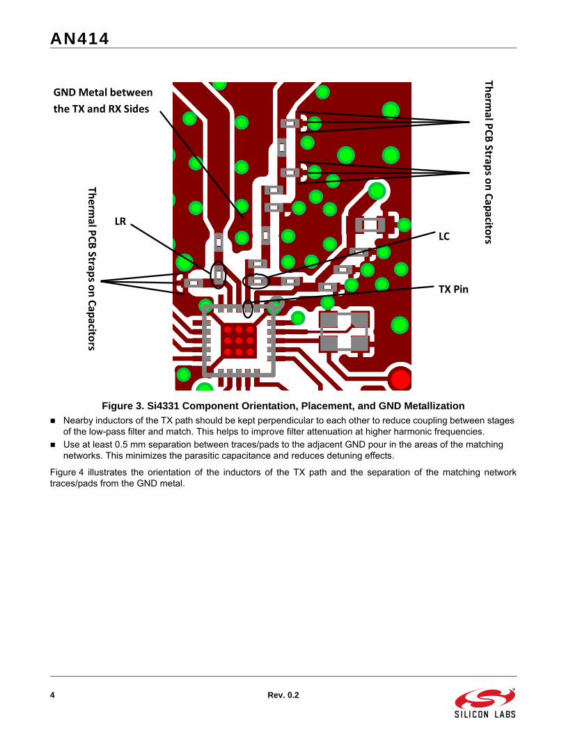
The choke inductor (LC) should be placed as close to the TX pin of the RF IC as possible (even if this means the RX is further away).
The parallel inductor in the RX path (LR) should be perpendicular to the choke inductor (LC) in the TX path because this will reduce TX-to-RX coupling.
The TX and RX sections should be separated by a GND metal on the top layer to reduce coupling.
The neighboring matching network components should be placed as close to each other as possible in order to minimize any PCB parasitic capacitance to ground and the series parasitic inductances between the components.
Increase the grounding effect in the thermal straps used with capacitors. In addition, thicken the trace near the GND pin of these capacitors. This will minimize series parasitic inductance between the ground pour and the GND pins. Additional vias placed close to the GND pin of capacitors (thus connecting it to the bottom layer GND plane) will further help reduce these effects.
Figure 3 illustrates the positioning and orientation of the LC and LR components, the separating GND metalbetween the TX and RX sections, and thermal strapping on the shunt capacitors.
Crystal
RF IC
VDD Filter Capacitors
PCB Vias
TX Section
RX Section
Ground
Metallization
AN414
4 Rev. 0.2
Figure 3. Si4331 Component Orientation, Placement, and GND Metallization
Nearby inductors of the TX path should be kept perpendicular to each other to reduce coupling between stages of the low-pass filter and match. This helps to improve filter attenuation at higher harmonic frequencies.
Use at least 0.5 mm separation between traces/pads to the adjacent GND pour in the areas of the matching networks. This minimizes the parasitic capacitance and reduces detuning effects.
Figure 4 illustrates the orientation of the inductors of the TX path and the separation of the matching networktraces/pads from the GND metal.
TX Pin
LC
LR
GND Metal between
the TX and RX Sides
Therm
al PCB Stra
ps o
n Cap
acito
rs
Therm
al PCB Stra
ps o
n Cap
acito
rs
AN414
Rev. 0.2 5
Figure 4. TX Side Inductor Orientation, Thermal Strapping, and Separation from GND The smaller VDD bypass capacitors (C1 = 33 pF and C2 = 100 pF) should be kept as close to the VDD pin as
possible.
The exposed pad footprint for the paddle of the RF IC should use as many vias as possible to ensure good grounding and heatsink capability. In the reference designs, there are nine vias, each with 12 mil diameter. The paddle ground should also be connected to the top layer GND metal (if possible) to further improve RF grounding; this may be accomplished with diagonal trace connections through the corners of the RFIC footprint.
The crystal should be placed as close as possible to the RFIC to ensure that wire parasitic capacitances are kept as low as possible; this reduces any frequency offsets that may occur.
Place ground metal between the crystal and the VDD trace to reduce coupling effects.
Figure 5 illustrates the grounding of the RFIC, the crystal, and VDD filter capacitor positions, and the isolatingground metal between the VDD trace and the crystal.
LM2
LM
L0
LC
Separatio
n of Traces fro
m GND
AN414
6 Rev. 0.2
Figure 5. RFIC GND Vias and GND Metallization
To achieve good RF ground on the layout, it is recommended to add large, continuous GND metallization on the top layer in the area of the RF section (at a minimum). Better performance may be obtained if this is applied to the entire PCB. To provide a good RF ground, the RF voltage potentials should be equal along the entire GND area because this helps maintain good VDD filtering and provides a good ground plane for a monopole antenna. Ideally, gaps should be filled with GND metal, and the resulting sections on the top and bottom layers should be connected with as many vias as possible.
The area under the matching network (on the bottom layer) should be filled with ground metal because this helps reduce or eliminate radiation emissions. Board routing and wiring should not be placed in this region to prevent coupling effects with the matching network. It is also recommended that the GND return path between the GND vias of the TX LPF/Match and the GND vias of the RFIC paddle should not be blocked in any way; the return currents should see a clear unhindered pathway through the GND plane to the back of the RFIC.
Figures 6 and 7 illustrate the GND metal filled sections on the entire 4431-T-B1_B test card PCB. The top andbottom layers are shown.
Connection to GND through more vias
VDD Pin
GND Metal between the Crystal and VDD
Crystal
C2
C1
AN414
Rev. 0.2 7
Figure 6. Ground Poured Sections with PCB Vias around the Matching Network (Top Layer)
Figure 7. Ground Poured Sections with PCB Vias (Bottom Layer)
AN414
8 Rev. 0.2
To reduce sensitivity to PCB thickness variation, use 50 grounded coplanar lines wherever possible to connect the SMA connector(s) to the matching network and/or the RF switch. This also reduces radiation and coupling effects. The interconnections between the elements are not considered transmission lines because their lengths are much shorter than the wavelength and, thus, their impedance is not critical. As a result, their recommended width is the smallest possible (i.e. equal to the width of the pad of the applied components). In this way, the parasitic capacitances to ground can be minimized. In the case of the 4431-T-B1_B type test card, the only routes where 50 coplanar transmission line is used are between the output of the matching networks and the SMA connectors. Examples for the trace dimensions are shown in Table 1.
Figure 8 illustrates the 50 grounded coplanar line of the TX side on the 4431-T-B1_B test cards.
Figure 8. 50 Grounded Coplanar Line on 1.5 mm Thick Substrate
Figure 9. Grounded Coplanar Line Parameters
Table 1. Parameters for 50 Grounded Coplanar Lines
f 240−960 MHz
T 0.018−0.035 mm
Er 4.6
H 1.5 mm 0.26 mm*
G 0.25 mm 0.64 mm
W 1.26 mm 0.45 mm
*Note: For four-layer PCBs, the thickness between the top and the next inner layer should be taken into account.
AN414
Rev. 0.2 9
2.1.3. Direct Tie Type Matching Network Layout Based upon the 4431-T-B1_D Test Card(Single Antenna without RF Switch)
For reference, layout examples shown in this section are based upon the layout of the 4431-T-B1_D RF test cards.These boards contain a single antenna, and the TX and RX paths are connected directly together, without the useof an RF switch.
The schematic of the Direct Tie type matching network is shown in Figure 10. For this type of matching, anadditional inductor is necessary at the RX side, forming a four-element RX matching network (described in “AN436:Si4030/4031/4430/4431 PA Matching”).
During TX mode operation, the built-in LNA protection circuit should be enabled by setting the lna_sw bit of the TXPower register 6Dh to “1” (see “AN440: Si4430/31/32 Register Descriptions”). In this case, the dc path from theoutput of the matching network to GND is not blocked through the RX side; so, a dc blocking capacitor (CC1) isnecessary.
In the case of Direct Tie type matching, coupling between the RX and TX sides is not critical since no harmonicleakage through the coupled RX path occurs; both of them are filtered after the common connection point.
Figure 10. Schematic of the Direct Tie Type Matching Network
AN414
10 Rev. 0.2
2.1.4. Layout Design Guidelines
The principles in this case are the same as for Split type matching, except for the following issues:
To minimize the parasitics (i.e., the length) of the trace connecting the RX and TX sides, the RX side components are closer to the TX side components. Also, because of this, the nearby inductors are not perpendicular to each other.
The trace parasitics are very critical for the connection of LR2; so, the shortest traces possible should be used for connecting LR2 to the TX side.
Since the RX-TX coupling is not critical, there is not any separating GND metal between the two sides.
Figure 11 illustrates the positioning and orientation of components and ground pour flooding.
Figure 11. Direct Tie Matching Network Layout Structure
TX Section
Ground Metallization
TX Pin
LC
RX Section
L0
LR2
LR
DC Blocking
Capacitor
AN414
Rev. 0.2 11
2.2. Guidelines for Layout Design when Using the Si4432
For the versions of RF test cards using the Si4432 RFIC (i.e., +20 dBm PA), similar general layout guidelines canbe applied as described for the Si4431 RFIC (i.e., +13 dBm PA). However, some minimal additional filtering andcircuitry must be implemented.
The increased TX output power of the Si4432 chip is accompanied by a corresponding increase in the absolutelevel of harmonic signals. Since most regulatory standards (e.g. FCC, ETSI, ARIB, etc.) require the harmonicsignals to be attenuated below some absolute power level (in watts or dBm), the amount of low-pass filteringrequired is generally greater on an RF test card using an Si4432 chip. Thus, the RF test card layout for the Si4432RFIC may contain a slightly higher number of components in the L-C lowpass filter.
Further, due to the increase in output power, it is necessary to pay closer attention to the shape and amplitude ofthe voltage waveform at the TX output pin of the device. Silicon Labs recommends that a harmonic terminationcircuit be placed in a parallel shunt-to-GND configuration at the input of the lowpass filter. This harmonictermination circuit helps maintain the desired voltage waveform at the TX output pin by providing a goodimpedance termination at very high harmonic frequencies. For further information on this subject, refer to “AN435:Si4032/4432 PA Matching”.
Unlike the Si4431, the test cards for the Si4432 are manufactured on a four-layer PCB. The purpose of this is toallow most traces to be placed on the inner layers while the outer layers function as shields for further reduction ofthe radiated levels of harmonics.
2.2.1. Switch Type Matching Network Layout Based upon the 4432-T-B1_C Test Card(Single Antenna with RF Switch)
For reference, examples shown in this section are based upon the layout of the 4432-T-B1_C RF test cards. Theseboards contain a single antenna and an RF switch to select between the TX and RX paths. The schematic of theSwitch type matching network for the Si4432 RevB1 is shown in Figure 12.
Figure 12. Schematic of the Switch Type Matching Network for the Si4432 Rev B1
AN414
12 Rev. 0.2
2.2.2. Layout Design Guidelines
When using a TX/RX switch, or a switch to select antennas in an antenna diversity implementation, a series capacitor may be required on all ports (e.g., TX, RX, Antenna) of the switch to block the dc patch between the switch and the ground. Refer to the exact requirements and specifications of the switch used in the application.
RF switches may themselves behave in a slightly non-linear fashion, resulting in some re-generation of harmonic energy regardless of the cleanliness of the input signal to the switch. Thus it may be necessary to move a portion of the TX lowpass filter to after the RF switch (i.e., just prior to the antenna) in order to further attenuate these re-generated harmonic signals.
If the RX side matching network is relatively far from the RF switch then the connecting trace should be a 50? grounded coplanar line.
The area between the RX and TX sides should be filled with GND metal to increase the isolation (just as in case of the Split type design).
Figure 13 demonstrates the positioning and orientation of components, ground flooding, and thermal strapping.
Figure 13. Si4432 Switch Type Matching, Component Orientation, Placement, and GND Metallization
DC Blocking Capacitors
Filter Section after the RF Switch
RF Switch
Harmonic Termination Circuit
Filter Section before the RF Switch
50 Ohm Grounded Coplanar Line for 0.26 mm Substrate Thickness
Isolating GND Metal
AN414
Rev. 0.2 13
The return path to GND of the harmonic termination circuit is important. This trace and current path should be keptas short as possible and should be allowed to return directly to the GND paddle of the RFIC; it should be connectedto the GND metal only at that point. Also, to avoid coupling with the matching network itself, it should be routed onthe second inner layer under the matching network, not on the first one (the first inner layer should be filled withground metal under the matching network). Figure 14 demonstrates the dc return path of the harmonic terminationcircuit.
Figure 14. DC Return Path on the Second Inner Layer(The First Inner Layer under the Top One is Suppressed)
2.2.3. Diversity Type Matching Network Layout Based upon the 4432-T-B1_A Test Card(Two Antennas with RF Switch)
The purpose of this type of test card is to demonstrate the Antenna Diversity feature of the EZRadioPRO RFICs.Antenna diversity is often used to provide better range in case of an obstructed environment where the range witha single antenna board configuration is lessened due to multipath fading and/or different RX antenna and TX fieldpolarizations.
Multipath fading causes nulls in the radiated field of the TX with 1/2 wavelength period. To compensate for this, theseparation distance of the antennas should be around 1/4 wavelength.
If the polarization of the radiated field is not parallel with the RX antenna, either because of the differentpolarization of the TX antenna or the polarization changes caused by reflections, then positioning the RX antennas
perpendicular to the each other can help. (Refer to “AN379: Antenna Diversity with EZRadioPRO®” for furtherinformation on this subject.)
As with the Switch type matching network, a portion of the TX lowpass filter (LPF) should be placed after the RFswitch to further attenuate any harmonics regenerated by the switch. Since, in this case, transmission is possibleon both antennas, the portion of the LPF should be inserted into both paths.
DC Return Trace of the Harmonic Termination Circuit on the Second Inner Layer
Isolation from the Rest of the GND
Harmonic Termination Circuit
Connect to GND under the Paddle of the RF IC
AN414
14 Rev. 0.2
The schematic of the Diversity type matching network is shown in Figure 15.
Figure 15. Schematic of the Diversity Type Matching Network2.2.4. Layout Design Guidelines
As discussed above, the distance between the two antennas on a Diversity type layout should be approximately 1/4 wavelength (on the 4432-T-B1_A test card, it is true for the higher ISM bands i.e. for 868/915 MHz), and the antennas should be perpendicular to each other.
If the antennas must be closer than 1/4 wavelength (due to PCB size) it is important to position them perpendicularly not only to compensate the polarization diversity but to minimize their effect on each other.
Figure 16 demonstrates antenna orientations and distances on the 4432-T-B1_A test card.
Figure 16. Antenna Orientations and Distance on the 4432-T-B1_A Test Card
Distance of the antennas ~1/4 wavelength at HB
90°
AN414
Rev. 0.2 15
3. Available Manufacturing Packs
Table 2 contains a partial list of the reference design packs available for download on www.silabs.com.
Table 2. Available Manufacturing Packs
Part Number Frequency [MHz]
Antenna Configuration
4031-T-B1 B 434 434 Single antenna
4031-T-B1 B 868 868 Single antenna
4032-T-B1 B 470 470 Single antenna
4032-T-B1 B 915 915 Single antenna
4330-T-B1 B 434 434 Single antenna
4330-T-B1 B 470 470 Single antenna
4330-T-B1 B 868 868 Single antenna
4330-T-B1 B 915 915 Single antenna
4330-T-B1 B 950 950 Single antenna
4430-T-B1 B 950 950 Separate TX and RX designed for lab testing
4430-T-B1 D 950 950 Single antenna implemented without RF switch
4431-T-B1 B 434 434 Separate TX and RX designed for lab testing
4431-T-B1 D 434 434 Single antenna implemented without RF switch
4431-T-B1 B 868 868 Separate TX and RX designed for lab testing
4431-T-B1 D 868 868 Single antenna implemented without RF switch
4432-T-B1 B 470 470 Separate TX and RX designed for lab testing
4431-T-B1 C 470 470 Single antenna implemented with RF switch
4431-T-B1 D 470 470 Single antenna implemented without RF switch
4431-T-B1 B 915 915 Separate TX and RX designed for lab testing
4431-T-B1 C 915 915 Single antenna implemented with RF switch
1 Is the choke inductor (LC) as close to the TX pin as possible?
2
Is the RX parallel inductor (LR) per-pendicular to the choke inductor (LC) in the TX path? (except for the Direct Tie type matching)
3
Is the TX and RX separated by a ground metal on the top layer? (except for the Direct Tie type match-ing)
4Are the neighboring matching net-work components as close to each other as possible?
5 Are there more thermal straps used with the capacitors?
6 Are the TX path inductors perpendicular to each other?
7Is there at least 0.5 mm separation in the matching between the traces/pads and the GND metal?
AN414
Rev. 0.2 17
8Are the smallest value VDD filter capacitors kept closer to the VDD pin of the RF IC?
9 Does exposed pad footprint use more vias?
10 Is the crystal as close to the RF IC as possible?
11 Does ground metal exist between the crystal and the VDD feed?
12Was large, continuous GND metallization added to at least the RF sections?
13
Was the area on the bottom layer under the matching network filled with GND metal and was wiring and routing avoided in this region?
14
Were 50 grounded coplanar lines used for connecting the matching network, the switch and/or the SMA connector(s)?
AN414
18 Rev. 0.2
4.2. Additional Concerns for Direct Tie Matching
15Is the length of the trace connecting the RX and TX sides minimal?
16Is LR2 connected with as short traces as possible?
17
Is an additional dc blocking capacitor added to the output of the matching network to block the dc path in RX mode?
AN414
Rev. 0.2 19
4.3. Additional Concerns for the Si4432 and the Switch and Diversity Type Matching
18Was the additional harmonic termination circuit is added into the TX path?
19
Were series capacitors added to the TX path to block the dc when a TX/RX switch (or Diversity switch) is used?
20
Was 50 grounded coplanar line used for connecting the RX side matching to the RF switch (if they are far from each other)?
21Was the area between the RX and TX sides filled with GND metal?
22Was the dc return path of the harmonic termination circuit constructed properly?
AN414
20 Rev. 0.2
23Are the antennas perpendicular to each other?
24Is the distance of the antennas approximately 1/4 wavelength?
AN414
Rev. 0.2 21
DOCUMENT CHANGE LIST
Revision 0.1 to Revision 0.2 Updated to latest reference designs
DisclaimerSilicon Laboratories intends to provide customers with the latest, accurate, and in-depth documentation of all peripherals and modules available for system and software implementers using or intending to use the Silicon Laboratories products. Characterization data, available modules and peripherals, memory sizes and memory addresses refer to each specific device, and "Typical" parameters provided can and do vary in different applications. Application examples described herein are for illustrative purposes only. Silicon Laboratories reserves the right to make changes without further notice and limitation to product information, specifications, and descriptions herein, and does not give warranties as to the accuracy or completeness of the included information. Silicon Laboratories shall have no liability for the consequences of use of the information supplied herein. This document does not imply or express copyright licenses granted hereunder to design or fabricate any integrated circuits. The products must not be used within any Life Support System without the specific written consent of Silicon Laboratories. A "Life Support System" is any product or system intended to support or sustain life and/or health, which, if it fails, can be reasonably expected to result in significant personal injury or death. Silicon Laboratories products are generally not intended for military applications. Silicon Laboratories products shall under no circumstances be used in weapons of mass destruction including (but not limited to) nuclear, biological or chemical weapons, or missiles capable of delivering such weapons.
Trademark InformationSilicon Laboratories Inc., Silicon Laboratories, Silicon Labs, SiLabs and the Silicon Labs logo, CMEMS®, EFM, EFM32, EFR, Energy Micro, Energy Micro logo and combinations thereof, "the world’s most energy friendly microcontrollers", Ember®, EZLink®, EZMac®, EZRadio®, EZRadioPRO®, DSPLL®, ISOmodem ®, Precision32®, ProSLIC®, SiPHY®, USBXpress® and others are trademarks or registered trademarks of Silicon Laboratories Inc. ARM, CORTEX, Cortex-M3 and THUMB are trademarks or registered trademarks of ARM Holdings. Keil is a registered trademark of ARM Limited. All other products or brand names mentioned herein are trademarks of their respective holders.
http://www.silabs.com
Silicon Laboratories Inc.400 West Cesar ChavezAustin, TX 78701USA
Simplicity StudioOne-click access to MCU tools, documentation, software, source code libraries & more. Available for Windows, Mac and Linux!