+ All Categories
Home > Documents > F2255 Datasheet - Renesas Electronics Corporation

F2255 Datasheet - Renesas Electronics Corporation

Date post: 15-Feb-2022
Category:
Upload: others
View: 4 times
Download: 0 times
Share this document with a friend
27
Voltage Variable RF Attenuator 1MHz to 3000MHz © 2018 Renesas Electronics Corporation 1 May 7, 2021 F2255 Datasheet GENERAL DESCRIPTION The F2255 is a low insertion loss Voltage Variable RF Attenuator (VVA) designed for a multitude of wireless and other RF applications. This device covers a broad frequency range from 1MHz to 3000MHz. In addition to providing low insertion loss, the F2255 provides excellent linearity performance over its entire voltage control and attenuation range. The F2255 uses a single positive supply voltage of 3.15V to 5.25V. Other features include the VMODE pin allowing either positive or negative voltage control slope vs attenuation and multi-directional operation meaning the RF input can be applied to either RF1 or RF2 pins. Control voltage ranges from 0V to 3.6V using either positive or negative control voltage slope. COMPETITIVE ADVANTAGE The F2255 provides extremely low insertion loss and superb IP3, IP2, Return Loss and Slope Linearity across the control range. Comparing to competitive VVAs this device is better as follows: Operation down to 1MHz Insertion Loss @ 500MHz: 1.1dB Maximum Attenuation Slope: 33dB/Volt Minimum Output IP3: 35dBm Minimum Input IP2: 74dBm High Operating Temperature: +105°C APPLICATIONS Base Station 2G, 3G, 4G Portable Wireless Repeaters and E911 systems Digital Pre-Distortion Point to Point Infrastructure Public Safety Infrastructure Satellite Receivers and Modems WIMAX Receivers and Transmitters Military Radios covering HF, VHF, UHF RFID handheld and portable readers Cable Infrastructure Wireless LAN Test / ATE Equipment FEATURES Low Insertion Loss: 1.1dB @ 500MHz Typical / Min IIP3: 60dBm / 46dBm Typical / Min IIP2: 98dBm / 74dBm 33dB Attenuation Range Bi-directional RF ports +36dBm Input P1dB compression VMODE pin allows either positive or negative control response Linear-in-dB attenuation characteristic Supply voltage: 3.15V to 5.25V VCTRL range: 0V to 3.6V using 5V supply +105°C max operating temperature 3mm x 3mm, 16-pin QFN package DEVICE BLOCK DIAGRAM ORDERING INFORMATION PART# MATRIX Part# RF Freq Range (MHz) Insertion Loss (dB) IIP3 (dBm) Pinout Compatibility F2250 50 - 6000 1.4 (at 2GHz) +65 RFMD F2255 1 - 3000 1.1 (at 500MHz) +60 F2258 50 - 6000 1.4 (at 2GHz) +65 Hittite RF1 RF2 Control V DD V MODE V CTRL F2255NLGK8 0.9 mm height package Green Tape & Reel RF product Line
Transcript

Voltage Variable RF Attenuator 1MHz to 3000MHz

© 2018 Renesas Electronics Corporation 1 May 7, 2021

F2255 Datasheet

GENERAL DESCRIPTION The F2255 is a low insertion loss Voltage Variable RF Attenuator (VVA) designed for a multitude of wireless and other RF applications. This device covers a broad frequency range from 1MHz to 3000MHz. In addition to providing low insertion loss, the F2255 provides excellent linearity performance over its entire voltage control and attenuation range. The F2255 uses a single positive supply voltage of 3.15V to 5.25V. Other features include the VMODE pin allowing either positive or negative voltage control slope vs attenuation and multi-directional operation meaning the RF input can be applied to either RF1 or RF2 pins. Control voltage ranges from 0V to 3.6V using either positive or negative control voltage slope.

COMPETITIVE ADVANTAGE The F2255 provides extremely low insertion loss and superb IP3, IP2, Return Loss and Slope Linearity across the control range. Comparing to competitive VVAs this device is better as follows:

Operation down to 1MHz

Insertion Loss @ 500MHz: 1.1dB

Maximum Attenuation Slope: 33dB/Volt

Minimum Output IP3: 35dBm

Minimum Input IP2: 74dBm

High Operating Temperature: +105°C

APPLICATIONS • Base Station 2G, 3G, 4G • Portable Wireless • Repeaters and E911 systems • Digital Pre-Distortion • Point to Point Infrastructure • Public Safety Infrastructure • Satellite Receivers and Modems • WIMAX Receivers and Transmitters • Military Radios covering HF, VHF, UHF • RFID handheld and portable readers • Cable Infrastructure • Wireless LAN • Test / ATE Equipment

FEATURES • Low Insertion Loss: 1.1dB @ 500MHz • Typical / Min IIP3: 60dBm / 46dBm • Typical / Min IIP2: 98dBm / 74dBm • 33dB Attenuation Range • Bi-directional RF ports • +36dBm Input P1dB compression • VMODE pin allows either positive or negative

control response • Linear-in-dB attenuation characteristic • Supply voltage: 3.15V to 5.25V • VCTRL range: 0V to 3.6V using 5V supply • +105°C max operating temperature • 3mm x 3mm, 16-pin QFN package

DEVICE BLOCK DIAGRAM

ORDERING INFORMATION

PART# MATRIX

Part# RF Freq Range (MHz)

Insertion Loss (dB)

IIP3 (dBm)

Pinout Compatibility

F2250 50 - 6000 1.4 (at 2GHz) +65 RFMD

F2255 1 - 3000 1.1 (at 500MHz) +60

F2258 50 - 6000 1.4 (at 2GHz) +65 Hittite

RF1 RF2

Control

V DD

V MO

DE

V CTR

L

F2255NLGK8

0.9 mm height package

Green

Tape & Reel

RF product Line

Voltage Variable RF Attenuator 1MHz to 3000MHz

© 2018 Renesas Electronics Corporation 2 May 7, 2021

F2255 Datasheet

ABSOLUTE MAXIMUM RATINGS Parameter / Condition Symbol Min Max Units

VDD to GND VDD -0.3 5.5 V VMODE to GND VMODE -0.3 Minimum ( VDD, 3.9 ) V VCTRL to GND VDD = 0V to 5.25V VCTRL -0.3 Minimum ( VDD, 4.0 ) V RF1, RF2 to GND VRF -0.3 0.3 V RF1 or RF2 Input Power applied for 24 hours maximum (VDD applied @ 2GHz and Tc=+85°C) PMAX24 30 dBm

RF1 or RF2 Continuous Operating Power PMAX_OP See Figure 1 dBm Maximum Junction Temperature TJMAX +150 °C Storage Temperature Range TST -65 +150 °C Lead Temperature (soldering, 10s) TLEAD +260 °C ESD Voltage– HBM (Per ESD STM5.1-2007) VESDHBM Class 2 ESD Voltage – CDM (Per ESD STM5.3.1-2009) VESDCDM Class C3

FIGURE 1: MAXIMUM OPERATING RF INPUT POWERS VS. RF FREQUENCY

Stresses above those listed above may cause permanent damage to the device. Functional operation of the device at these or any other conditions above those indicated in the operational section of this specification is not implied. Exposure to absolute maximum rating conditions for extended periods may affect device reliability.

PACKAGE THERMAL AND MOISTURE CHARACTERISTICS ΘJA (Junction – Ambient) 80.6°C/W ΘJC (Junction – Case) The Case is defined as the exposed paddle 5.1°C/W Moisture Sensitivity Rating (Per J-STD-020) MSL 1

Voltage Variable RF Attenuator 1MHz to 3000MHz

© 2018 Renesas Electronics Corporation 3 May 7, 2021

F2255 Datasheet

F2255 OPERATING CONDITIONS

Parameter Symbol Condition Min Typ Max Units Operating Frequency Range FRF 1 3000 MHz Supply Voltage VDD 3.15 5.25 V

VMODE Logic VIH VDD > 3.9V 1.17 3.6 2 V VDD = 3.15 to 3.9V 1.17 VDD -0.3V

VIL 0 0.63

VCTRL Range VCTRL VDD = 3.9V to 5.25V 0 3.6 V VDD = 3.15V to 3.9V 0 VDD-0.3 Supply Current IDD 0.50 1 1.15 2 mA Logic Current IMODE -1.0 38 μA ICTRL Current ICTRL -1.0 14 μA

RF Operating Power 3 PMAXCW See Figure 1 dBm

RF1 Port Impedance ZRF1 50 Ω

RF2 Port Impedance ZRF2 50 Operating Temperature Range TCASE Exposed Paddle

Temperature -40 +105 °C

Operating Conditions Notes: 1 – Items in min/max columns in bold italics are Guaranteed by Test. 2 – Items in min/max columns that are not bold/italics are Guaranteed by Design Characterization. 3 – Refer to the Maximum Operating RF Input Power vs. RF Frequency curves in Figure 1.

Voltage Variable RF Attenuator 1MHz to 3000MHz

© 2018 Renesas Electronics Corporation 4 May 7, 2021

F2255 Datasheet

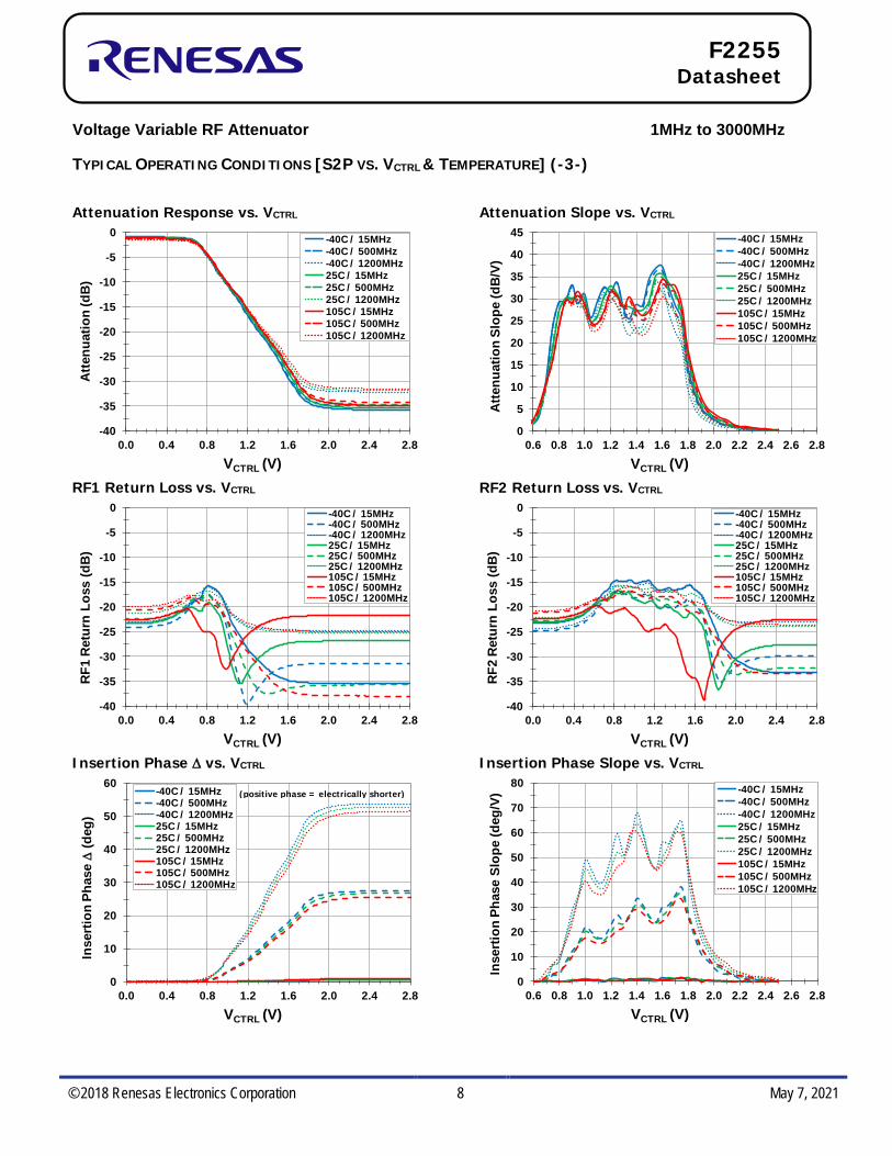
F2255 SPECIFICATIONS Refer to EVKit / Applications Circuit, VDD = +3.3V, TC = +25°C, signals applied to RF1 input, FRF = 500MHz, minimum attenuation, PIN = 0dBm for small signal parameters, +20dBm for single tone linearity tests, +20dBm per tone for two tone tests, two tone delta frequency = 80MHz, PCB board traces and connector losses are de-embedded unless otherwise noted. Refer to Typical Operating Curves for performance over entire frequency band.

Parameter Symbol Condition Min Typ Max Units Insertion Loss, IL AMIN Minimum Attenuation 1.1 1.7 1 dB Maximum attenuation AMAX 33 34.6 dB

Insertion Phase Δ ΦΔMAX At 36dB attenuation

relative to Insertion Loss 27 deg

ΦΔMID At 18dB attenuation relative to Insertion Loss 8

Input 1dB Compression 3 P1dB 36 dBm

Minimum RF1 Return Loss over control voltage range S11

20MHz 23

dB 500MHz 22 2000MHz 23 3000MHz 30

Minimum RF2 Return Loss over control voltage range S22

20MHz 23

dB 500MHz 22 2000MHz 23 3000MHz 24

Input IP3 IIP3 60 dBm Input IP3 over Attenuation IIP3ATTEN All attenuation settings 44 2 46

Minimum Output IP3 OIP3MIN Maximum attenuation 35

Input IP2 IIP2 PIN + IM2dBC, IM2 term is F1+F2 98 dBm

Minimum Input IP2 IIP2MIN All attenuation settings 74 dBm Input IH2 HD2 PIN + H2dBc 82 dBm Input IH3 HD3 PIN + (H3dBc/2) 49 dBm

Settling Time TSETTL0.1dB Any 1dB step in the 0dB to 33dB control range 50% VCTRL to RF settled to within ± 0.1dB

15 μSec

Specification Notes: 1 – Items in min/max columns in bold italics are Guaranteed by Test. 2 – Items in min/max columns that are not bold/italics are Guaranteed by Design Characterization. 3 – The input 1dB compression point is a linearity figure of merit. Refer to Absolute Maximum Ratings section along with Figure 1 for the maximum RF input power vs. RF frequency.

Voltage Variable RF Attenuator 1MHz to 3000MHz

© 2018 Renesas Electronics Corporation 5 May 7, 2021

F2255 Datasheet

TYPICAL OPERATING CURVES

UNLESS OTHERWISE NOTED, THE FOLLOWING CONDITIONS APPLY:

• VDD = +3.3V or +5.0V • TC = +25ºC • VMODE = 0V • RF trace and connector losses are de-embedded for S-parameters • Pin = 0dBm for all small signal tests • Pin = +20dBm for single tone linearity tests (RF1 port driven) • Pin = +20dBm/tone for two tone linearity tests (RF1 port driven) • Two tone frequency spacing = 80MHz

Voltage Variable RF Attenuator 1MHz to 3000MHz

© 2018 Renesas Electronics Corporation 6 May 7, 2021

F2255 Datasheet

TYPICAL OPERATING CONDITIONS [S2P BROADBAND PERFORMANCE] (-1-) Attenuation vs. VCTRL

Attenuation vs. Frequency

Attenuation Delta to 25C vs. VCTRL

-40

-35

-30

-25

-20

-15

-10

-5

0

0.0 0.4 0.8 1.2 1.6 2.0 2.4 2.8

Atte

nuat

ion

(dB

)

VCTRL (Volts)

25C / 10MHz25C / 50MHz25C / 100MHz25C / 250MHz25C / 500MHz25C / 900MHz25C / 1200MHz25C / 1900MHz25C / 2700MHz

-45-40-35-30-25-20-15-10

-50

0 500 1000 1500 2000 2500 3000

Atte

nuat

ion

(dB

)

Frequency (MHz)

25C / 0.0V 25C / 0.8V 25C / 1.0V25C / 1.2V 25C / 1.4V 25C / 1.6V25C / 1.8V 25C / 2.2V 25C / 2.8V

-3

-2

-1

0

1

2

3

4

0.0 0.4 0.8 1.2 1.6 2.0 2.4 2.8

Atte

nuat

ion

Erro

r (dB

)

VCTRL (V)

-40C / 11MHz-40C / 251MHz-40C / 900MHz105C / 11MHz105C / 251MHz105C / 900MHz

Voltage Variable RF Attenuator 1MHz to 3000MHz

© 2018 Renesas Electronics Corporation 7 May 7, 2021

F2255 Datasheet

TYPICAL OPERATING CURVES [S2P VS. VCTRL] (-2-)

Attenuation vs. VCTRL

RF1 Return Loss vs. VCTRL

Insertion Phase ∆ vs. VCTRL

Attenuation Slope vs. VCTRL

RF2 Return Loss vs. VCTRL

Insertion Phase Slope vs. VCTRL

-40

-35

-30

-25

-20

-15

-10

-5

0

0.0 0.4 0.8 1.2 1.6 2.0 2.4 2.8

Atte

nuat

ion

(dB)

4MHz15MHz60MHz200MHz600MHz1200MHz2100MHz

VCTRL (V)

25C

-40

-35

-30

-25

-20

-15

-10

-5

0

0.0 0.4 0.8 1.2 1.6 2.0 2.4 2.8

RF1

Retu

rn L

oss

(dB)

4MHz 15MHz60MHz 200MHz600MHz 1200MHz2100MHz

VCTRL (V)

25C

0

10

20

30

40

50

60

70

80

0.0 0.4 0.8 1.2 1.6 2.0 2.4 2.8

Inse

rtion

Pha

se ∆

(deg

)

4MHz15MHz60MHz200MHz600MHz1200MHz2100MHz

VCTRL (V)

25C

0

5

10

15

20

25

30

35

40

0.6 0.8 1.0 1.2 1.4 1.6 1.8 2.0 2.2

Atte

nuat

ion

Slop

e (d

B/V)

4MHz 15MHz60MHz 200MHz600MHz 1200MHz2100MHz

VCTRL (V)

25C

-40

-35

-30

-25

-20

-15

-10

-5

0

0.0 0.4 0.8 1.2 1.6 2.0 2.4 2.8

RF2

Retu

rn L

oss

(dB)

4MHz 15MHz60MHz 200MHz600MHz 1200MHz2100MHz

VCTRL (V)

25C

-10

10

30

50

70

90

110

0.6 0.8 1.0 1.2 1.4 1.6 1.8 2.0 2.2

Inse

rtion

Pha

se S

lope

(deg

/V) 4MHz 15MHz 60MHz

200MHz 600MHz 1200MHz2100MHz

VCTRL (V)

25C(positive phase = electrically shorter)

Voltage Variable RF Attenuator 1MHz to 3000MHz

© 2018 Renesas Electronics Corporation 8 May 7, 2021

F2255 Datasheet

TYPICAL OPERATING CONDITIONS [S2P VS. VCTRL & TEMPERATURE] (-3-)

Attenuation Response vs. VCTRL

RF1 Return Loss vs. VCTRL

Insertion Phase ∆ vs. VCTRL

Attenuation Slope vs. VCTRL

RF2 Return Loss vs. VCTRL

Insertion Phase Slope vs. VCTRL

-40

-35

-30

-25

-20

-15

-10

-5

0

0.0 0.4 0.8 1.2 1.6 2.0 2.4 2.8

Atte

nuat

ion

(dB)

VCTRL (V)

-40C / 15MHz-40C / 500MHz-40C / 1200MHz25C / 15MHz25C / 500MHz25C / 1200MHz105C / 15MHz105C / 500MHz105C / 1200MHz

-40

-35

-30

-25

-20

-15

-10

-5

0

0.0 0.4 0.8 1.2 1.6 2.0 2.4 2.8

RF1

Retu

rn L

oss

(dB)

VCTRL (V)

-40C / 15MHz-40C / 500MHz-40C / 1200MHz25C / 15MHz25C / 500MHz25C / 1200MHz105C / 15MHz105C / 500MHz105C / 1200MHz

0

10

20

30

40

50

60

0.0 0.4 0.8 1.2 1.6 2.0 2.4 2.8

Inse

rtion

Pha

se ∆

(deg

)

VCTRL (V)

-40C / 15MHz-40C / 500MHz-40C / 1200MHz25C / 15MHz25C / 500MHz25C / 1200MHz105C / 15MHz105C / 500MHz105C / 1200MHz

0

5

10

15

20

25

30

35

40

45

0.6 0.8 1.0 1.2 1.4 1.6 1.8 2.0 2.2 2.4 2.6 2.8

Atte

nuat

ion

Slop

e (d

B/V)

VCTRL (V)

-40C / 15MHz-40C / 500MHz-40C / 1200MHz25C / 15MHz25C / 500MHz25C / 1200MHz105C / 15MHz105C / 500MHz105C / 1200MHz

-40

-35

-30

-25

-20

-15

-10

-5

0

0.0 0.4 0.8 1.2 1.6 2.0 2.4 2.8

RF2

Retu

rn L

oss

(dB)

VCTRL (V)

-40C / 15MHz-40C / 500MHz-40C / 1200MHz25C / 15MHz25C / 500MHz25C / 1200MHz105C / 15MHz105C / 500MHz105C / 1200MHz

0

10

20

30

40

50

60

70

80

0.6 0.8 1.0 1.2 1.4 1.6 1.8 2.0 2.2 2.4 2.6 2.8

Inse

rtion

Pha

se S

lope

(deg

/V)

VCTRL (V)

-40C / 15MHz-40C / 500MHz-40C / 1200MHz25C / 15MHz25C / 500MHz25C / 1200MHz105C / 15MHz105C / 500MHz105C / 1200MHz

(positive phase = electrically shorter)

Voltage Variable RF Attenuator 1MHz to 3000MHz

© 2018 Renesas Electronics Corporation 9 May 7, 2021

F2255 Datasheet

TYPICAL OPERATING CONDITIONS [S2P VS. ATTENUATION & TEMPERATURE] (-4-) RF1 Return Loss vs. Attenuation

RF2 Return Loss vs. Attenuation

Insertion Phase Δ vs. Attenuation

RF1 Return Loss vs. Attenuation

RF2 Return Loss vs. Attenuation

Insertion Phase Δ vs. Attenuation

-40

-35

-30

-25

-20

-15

-10

-5

0

0 4 8 12 16 20 24 28 32 36

RF1

Retu

rn L

oss

(dB)

25C / 4MHz 25C / 15MHz25C / 60MHz 25C / 200MHz25C / 600MHz 25C / 1200MHz25C / 2100MHz

Attenuation (dB)

-40

-35

-30

-25

-20

-15

-10

-5

0

0 4 8 12 16 20 24 28 32 36

RF2

Retu

rn L

oss

(dB)

25C / 4MHz 25C / 15MHz25C / 60MHz 25C / 200MHz25C / 600MHz 25C / 1200MHz25C / 2100MHz

Attenuation (dB)

0

10

20

30

40

50

60

70

80

0 4 8 12 16 20 24 28 32 36

Inse

rtion

Pha

se ∆

(deg

)

25C / 4MHz25C / 15MHz25C / 60MHz25C / 200MHz25C / 600MHz25C / 1200MHz25C / 2100MHz

Attenuation (dB)

-40

-35

-30

-25

-20

-15

-10

-5

0

0 4 8 12 16 20 24 28 32 36

RF1

Retu

rn L

oss

(dB)

Attenuation (dB)

-40C / 15MHz-40C / 500MHz-40C / 1200MHz25C / 15MHz25C / 500MHz25C / 1200MHz105C / 15MHz105C / 500MHz105C / 1200MHz

-40

-35

-30

-25

-20

-15

-10

-5

0

0 4 8 12 16 20 24 28 32 36

RF2

Retu

rn L

oss

(dB)

Attenuation (dB)

-40C / 15MHz -40C / 500MHz-40C / 1200MHz 25C / 15MHz25C / 500MHz 25C / 1200MHz105C / 15MHz 105C / 500MHz105C / 1200MHz

0

10

20

30

40

50

60

0 4 8 12 16 20 24 28 32 36

Inse

rtion

Pha

se ∆

(deg

)

Attenuation (dB)

-40C / 15MHz-40C / 500MHz-40C / 1200MHz25C / 15MHz25C / 500MHz25C / 1200MHz105C / 15MHz105C / 500MHz105C / 1200MHz

(positive phase = electrically shorter)

Voltage Variable RF Attenuator 1MHz to 3000MHz

© 2018 Renesas Electronics Corporation 10 May 7, 2021

F2255 Datasheet

TYPICAL OPERATING CONDITIONS [S2P VS. FREQUENCY] (-5-)

Min. & Max. Attenuation vs. Frequency

Worst-Case RF1 Return Loss vs. Frequency

Max. Insertion Phase ∆ vs. Frequency

Min. & Max. Attenuation Slope vs. Frequency

Worst-Case RF2 Return Loss vs. Frequency

Gain Compression vs. Frequency

0

10

20

30

40

50

60

70

0 500 1000 1500 2000 2500 3000

Max

Inse

rtion

Pha

se ∆

(deg

)

Frequency (MHz)

-40C

25C

105C

0

5

10

15

20

25

30

35

40

0 500 1000 1500 2000 2500 3000

Min

/Max

ATT

N sl

ope

(dB/

V)

Frequency (MHz)

max slope

min slope

-2

-1.5

-1

-0.5

0

0.5

1

10 14 18 22 26 30 34 38

Gai

n Co

mpr

essi

on (d

B)

RF Input Power (dBm)

1MHz 125MHz 250MHz

500MHz 1000MHz 2700MHz(positive phase = electrically shorter)

VCTRL varied from 0.8V to 1.7V

Voltage Variable RF Attenuator 1MHz to 3000MHz

© 2018 Renesas Electronics Corporation 11 May 7, 2021

F2255 Datasheet

TYPICAL OPERATING CONDITIONS [S2P @ LOW FREQUENCY, GROUP DELAY] (-6-) Min. & Max. Attenuation vs. Low Frequency

Low-Frequency RF1 Return Loss vs. VCTRL

Group Delay vs. Frequency

Low-Frequency Attenuation vs. VCTRL

Low-Frequency RF2 Return Loss vs. VCTRL

-45

-40

-35

-30

-25

-20

-15

-10

-5

0

0 10 20 30 40 50 60 70 80 90 100

Atte

nuat

ion

(dB)

Frequency (MHz)

0.0V

2.8V

-40

-35

-30

-25

-20

-15

-10

-5

0

0.0 0.4 0.8 1.2 1.6 2.0 2.4 2.8

RF1

Retu

rn L

oss

(dB)

0.5MHz1.0MHz3.0MHz7.0MHz10.0MHz50.0MHz100.0MHz

VCTRL (V)

-100

-50

0

50

100

150

200

0 500 1000 1500 2000 2500 3000

Gro

up D

elay

(pic

osec

)

Frequency (MHz)

-40C / 0.8V-40C / 1.8V25C / 0.8V25C / 1.8V105C / 0.8V105C / 1.8V

-45

-40

-35

-30

-25

-20

-15

-10

-5

0

0.0 0.4 0.8 1.2 1.6 2.0 2.4 2.8

Atte

nuat

ion

(dB)

0.5MHz1.0MHz3.0MHz7.0MHz10.0MHz50.0MHz100.0MHz

VCTRL (V)

25C

-40

-35

-30

-25

-20

-15

-10

-5

0

0.0 0.4 0.8 1.2 1.6 2.0 2.4 2.8

RF2

Retu

rn L

oss

(dB)

0.5MHz1.0MHz3.0MHz7.0MHz10.0MHz50.0MHz100.0MHz

VCTRL (V)

Voltage Variable RF Attenuator 1MHz to 3000MHz

© 2018 Renesas Electronics Corporation 12 May 7, 2021

F2255 Datasheet

TYPICAL OPERATING CONDITIONS 500MHZ, VDD=3.3V [IP3, IP2, IH2, IH3 VS. VCTRL, VMODE] (-7-) Input IP3 vs. VCTRL

Input IP2 vs. VCTRL

2nd Harm Input Intercept Point vs. VCTRL

Output IP3 vs. VCTRL

Output IP2 vs. VCTRL

3rd Harm Input Intercept Point vs. VCTRL

20

30

40

50

60

70

80

0 0.4 0.8 1.2 1.6 2 2.4 2.8

Inpu

t IP3

(dB

m)

VCTRL (V)

-40C / Vmode = 0V25C / Vmode = 0V105C / Vmode = 0V-40C / Vmode = 3V25C / Vmode = 3V105C / Vmode = 3V

40

50

60

70

80

90

100

110

120

0 0.4 0.8 1.2 1.6 2 2.4 2.8

Inpu

t IP2

(dB

m)

VCTRL (V)

-40C / Vmode = 3V25C / Vmode = 3V105C / Vmode = 3V-40C / Vmode = 0V25C / Vmode = 0V105C / Vmode = 0V

50

60

70

80

90

100

110

120

130

140

0 0.4 0.8 1.2 1.6 2 2.4 2.8

IH2

(dB

m)

VCTRL (V)

-40C / Vmode = 0V25C / Vmode = 0V105C / Vmode = 0V-40C / Vmode = 3V25C / Vmode = 3V105C / Vmode = 3V

0

10

20

30

40

50

60

70

80

0 0.4 0.8 1.2 1.6 2 2.4 2.8

Out

put I

P3 (d

Bm

)

VCTRL (V)

-40C / Vmode = 0V25C / Vmode = 0V105C / Vmode = 0V-40C / Vmode = 3V25C / Vmode = 3V105C / Vmode = 3V

30

40

50

60

70

80

90

100

110

120

0 0.4 0.8 1.2 1.6 2 2.4 2.8

Out

put I

P2 (d

Bm

)

VCTRL (V)

-40C / Vmode = 0V25C / Vmode = 0V105C / Vmode = 0V-40C / Vmode = 3V25C / Vmode = 3V105C / Vmode = 3V

10

20

30

40

50

60

70

80

90

0 0.4 0.8 1.2 1.6 2 2.4 2.8

IH3

(dB

m)

VCTRL (V)

-40C / Vmode = 0V25C / Vmode = 0V105C / Vmode = 0V-40C / Vmode = 3V25C / Vmode = 3V105C / Vmode = 3V

Voltage Variable RF Attenuator 1MHz to 3000MHz

© 2018 Renesas Electronics Corporation 13 May 7, 2021

F2255 Datasheet

TYPICAL OPERATING CONDITIONS 500MHZ, VDD=3.3V [IPX, IHX VS. VCTRL, RF1/RF2 DRIVEN] (-8-) Input IP3 vs. VCTRL

Input IP2 vs. VCTRL

2nd Harm Input Intercept Point vs. VCTRL

Output IP3 vs. VCTRL

Output IP2 vs. VCTRL

3rd Harm Input Intercept Point vs. VCTRL

20

30

40

50

60

70

80

0 0.4 0.8 1.2 1.6 2 2.4 2.8

Inpu

t IP3

(dB

m)

VCTRL (V)

-40C / RF1 Driven25C / RF1 Driven105C / RF1 Driven-40C / RF2 Driven25C / RF2 Driven105C / RF2 Driven

40

50

60

70

80

90

100

110

120

0 0.4 0.8 1.2 1.6 2 2.4 2.8

Inpu

t IP2

(dB

m)

VCTRL (V)

-40C / RF1 Driven25C / RF1 Driven105C / RF1 Driven-40C / RF2 Driven25C / RF2 Driven105C / RF2 Driven

50

60

70

80

90

100

110

120

130

0 0.4 0.8 1.2 1.6 2 2.4 2.8

IH2

(dB

m)

VCTRL (V)

-40C / RF1 Driven25C / RF1 Driven105C / RF1 Driven-40C / RF2 Driven25C / RF2 Driven105C / RF2 Driven

10

20

30

40

50

60

70

0 0.4 0.8 1.2 1.6 2 2.4 2.8

Out

put I

P3 (d

Bm

)

VCTRL (V)

-40C / RF1 Driven25C / RF1 Driven105C / RF1 Driven-40C / RF2 Driven25C / RF2 Driven105C / RF2 Driven

30

40

50

60

70

80

90

100

110

120

0 0.4 0.8 1.2 1.6 2 2.4 2.8

Out

put I

P2 (d

Bm

)

VCTRL (V)

-40C / RF1 Driven25C / RF1 Driven105C / RF1 Driven-40C / RF2 Driven25C / RF2 Driven105C / RF2 Driven

10

20

30

40

50

60

70

80

90

0 0.4 0.8 1.2 1.6 2 2.4 2.8

IH3

(dB

m)

VCTRL (V)

-40C / RF1 Driven25C / RF1 Driven105C / RF1 Driven-40C / RF2 Driven25C / RF2 Driven105C / RF2 Driven

Voltage Variable RF Attenuator 1MHz to 3000MHz

© 2018 Renesas Electronics Corporation 14 May 7, 2021

F2255 Datasheet

TYPICAL OPERATING CONDITIONS 500MHZ, VDD=3.3V [IP3, IP2, IH2, IH3 VS. ATTENUATION] (-9-) Input IP3 vs. Attenuation

Input IP2 vs. Attenuation

2nd Harm Input Intercept Point vs. Attenuation

Output IP3 vs. Attenuation

Output IP2 vs. Attenuation

3rd Harm Input Intercept Point vs. Attenuation

20

30

40

50

60

70

80

0 4 8 12 16 20 24 28 32 36

Inpu

t IP3

(dB

m)

Attenuation (dB)

-40C

25C

105C

40

50

60

70

80

90

100

110

120

0 4 8 12 16 20 24 28 32 36

Inpu

t IP2

(dB

m)

Attenuation (dB)

-40C25C105C

60

70

80

90

100

110

120

130

140

0 4 8 12 16 20 24 28 32 36

IH2

(dB

m)

Attenuation (dB)

-40C25C105C

10

20

30

40

50

60

70

80

0 4 8 12 16 20 24 28 32 36

Out

put I

P3 (d

Bm

)

Attenuation (dB)

-40C

25C

105C

30

40

50

60

70

80

90

100

110

120

0 4 8 12 16 20 24 28 32 36

Out

put I

P2 (d

Bm

)

Attenuation (dB)

-40C25C105C

10

20

30

40

50

60

70

80

90

0 4 8 12 16 20 24 28 32 36

IH3

(dB

m)

Attenuation (dB)

-40C25C105C

Voltage Variable RF Attenuator 1MHz to 3000MHz

© 2018 Renesas Electronics Corporation 15 May 7, 2021

F2255 Datasheet

TYPICAL OPERATING CONDITIONS 500MHZ, VDD=3.3V [IPX, IHX VS. ATTEN, RF1/RF2 DRIVEN] (-10-) Input IP3 vs. Attenuation

Input IP2 vs. Attenuation

2nd Harm Input Intercept Point vs. Attenuation

Output IP3 vs. Attenuation

Output IP2 vs. Attenuation

3rd Harm Input Intercept Point vs. Attenuation

20

30

40

50

60

70

80

0 4 8 12 16 20 24 28 32 36

Inpu

t IP3

(dB

m)

Attenuation (dB)

-40C / RF1 Driven25C / RF1 Driven105C / RF1 Driven-40C / RF2 Driven25C / RF2 Driven105C / RF2 Driven

40

50

60

70

80

90

100

110

120

0 4 8 12 16 20 24 28 32 36

Inpu

t IP2

(dB

m)

Attenuation (dB)

-40C / RF1 Driven25C / RF1 Driven105C / RF1 Driven-40C / RF2 Driven25C / RF2 Driven105C / RF2 Driven

50

60

70

80

90

100

110

120

130

0 4 8 12 16 20 24 28 32 36

IH2

(dB

m)

Attenuation(dB)

-40C / RF1 Driven25C / RF1 Driven105C / RF1 Driven-40C / RF2 Driven25C / RF2 Driven105C / RF2 Driven

10

20

30

40

50

60

70

0 4 8 12 16 20 24 28 32 36

Out

put I

P3 (d

Bm

)

Attenuation (dB)

-40C / RF1 Driven25C / RF1 Driven105C / RF1 Driven-40C / RF2 Driven25C / RF2 Driven105C / RF2 Driven

30

40

50

60

70

80

90

100

110

120

0 4 8 12 16 20 24 28 32 36

Out

put I

P2 (d

Bm

)

Attenuation (dB)

-40C / RF1 Driven25C / RF1 Driven105C / RF1 Driven-40C / RF2 Driven25C / RF2 Driven105C / RF2 Driven

10

20

30

40

50

60

70

80

90

0 4 8 12 16 20 24 28 32 36

IH3

(dB

m)

Attenuation (dB)

-40C / RF1 Driven25C / RF1 Driven105C / RF1 Driven-40C / RF2 Driven25C / RF2 Driven105C / RF2 Driven

Voltage Variable RF Attenuator 1MHz to 3000MHz

© 2018 Renesas Electronics Corporation 16 May 7, 2021

F2255 Datasheet

PACKAGE OUTLINE DRAWING The package outline drawings are located at the end of this document and are accessible from the Renesas website (see also 16-VFQFPN). The package information is the most current data available and is subject to change without revision of this document.

PINOUT & BLOCK DIAGRAM

GND 1

4

3

2NC

NC

RF1 RF2

12

9

10

NC

11 NC

GND

Control

RTN

GN

D

RTN

5 6 7 8

RTN

13

NC

141516

V DD

V MOD

E

V CTR

L

E.P.

Voltage Variable RF Attenuator 1MHz to 3000MHz

© 2018 Renesas Electronics Corporation 17 May 7, 2021

F2255 Datasheet

PIN DESCRIPTION

Pin Name Function 1, 7, 12 GND Ground these pins as close to the device as possible.

2, 4, 9, 11, 13 NC No internal connection. Renesas recommends connecting these pins to GND.

3 RF1 RF Port 1. Matched to 50 ohms. Must use an external AC coupling capacitor as close to the device as possible. For low frequency operation increase the capacitor value to result in a low reactance at the frequency of interest.

5, 6, 8 RTN Attenuator Ground Return. Each of these pins require a capacitor to GND to provide an RF return path. Place the capacitor as close to the device as possible.

10 RF2 RF Port 2. Matched to 50 ohms. Must use an external AC coupling capacitor as close to the device as possible. For low frequency operation increase the capacitor value to result in a low reactance at the frequency of interest.

14 VCTRL Attenuator control voltage. Apply a voltage in the range as specified in the Operating Conditions Table. See application section for details about VCTRL.

15 VDD Power supply input. Bypass to GND with capacitors close as possible to pin.

16 VMODE Attenuator slope control. Set to logic LOW to enable negative attenuation slope. Set to logic HIGH to enable positive attenuation slope.

— EP

Exposed Pad. Internally connected to GND. Solder this exposed pad to a PCB pad that uses multiple ground vias to achieve the specified RF performance.

Voltage Variable RF Attenuator 1MHz to 3000MHz

© 2018 Renesas Electronics Corporation 18 May 7, 2021

F2255 Datasheet

APPLICATIONS INFORMATION

Default Start-up VMODE must be tied to either GND or Logic High. If the VCTRL pin is left floating, the part will power up in the minimum attenuation state when VMODE = GND, or the maximum attenuation state when VMODE = High.

VCTRL The voltage level on the VCTRL pin is used to control the attenuation of the F2255. At VCTRL =0V, the attenuation is a minimum (maximum) in the negative (positive) slope mode. An increasing (decreasing) voltage on VCTRL produces an increasing (decreasing) attenuation respectively. The VCTRL pin has an on-chip pull-up ESD diode so VDD should be applied before VCTRL is applied (see Recommended Operating Conditions for details). If this sequencing is not possible, then resistor R2 in the application circuit should be set to 1kΩ to limit the current into the VCTRL pin.

VMODE

The VMODE pin is used to set the slope of the attenuation. The attenuation is varied by VCTRL as described in the next section. Setting VMODE to a logic LOW (HIGH) will set the attenuation slope to negative (positive). A negative (positive) slope is defined as an increased (decreased) attenuation with increasing VCTRL voltage. The Evaluation Kit provides an on-board jumper to manually set the VMODE. Install a jumper on header J2 from VMODE to the pin marked Lo (Hi) to set the device for a negative (positive) slope (see application circuit).

RF1 and RF2 Ports The F2255 is a bi-directional device, allowing RF1 or RF2 to be used as the RF input. RF1 has some enhanced linearity performance, and therefore should be used as the RF input, when possible, for best results. The F2255 has been designed to accept high RF input power levels; therefore, VDD must be applied prior to the application of RF power to ensure reliability. DC blocking capacitors are required on the RF pins and should be set to a value that results in a low reactance over the frequency range of interest.

Power Supplies The supply pin should be bypassed with external capacitors to minimize noise and fast transients. Supply noise can degrade noise figure and fast transients can trigger ESD clamps and cause them to fail. Supply voltage change or transients should have a slew rate smaller than 1V/20uS. In addition, all control pins should remain at 0V (+/-0.3V) while the supply voltage ramps or while it returns to zero.

Voltage Variable RF Attenuator 1MHz to 3000MHz

© 2018 Renesas Electronics Corporation 19 May 7, 2021

F2255 Datasheet

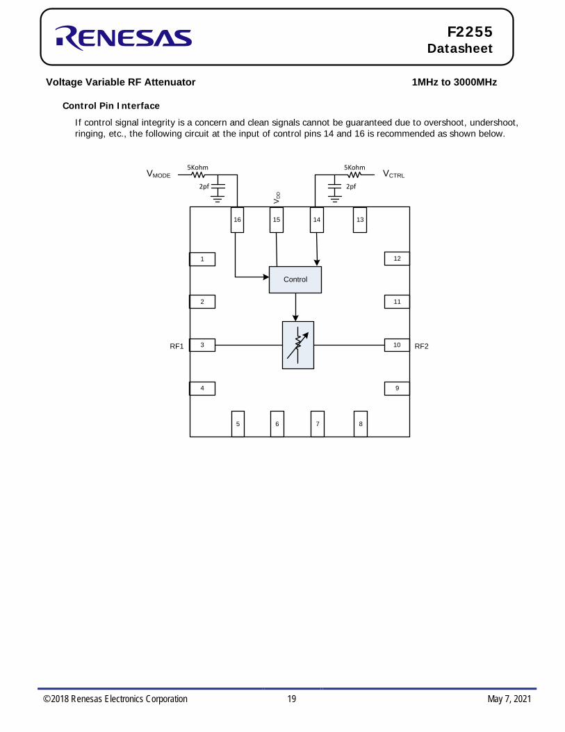
Control Pin Interface If control signal integrity is a concern and clean signals cannot be guaranteed due to overshoot, undershoot, ringing, etc., the following circuit at the input of control pins 14 and 16 is recommended as shown below.

1

4

3

2

12

9

10

11

Control

5 6 7 8

13141516

VMODE

2pf

5Kohm

2pf

5KohmVCTRL

V DD

RF1 RF2

Voltage Variable RF Attenuator 1MHz to 3000MHz

© 2018 Renesas Electronics Corporation 20 May 7, 2021

F2255 Datasheet

EVKIT / APPLICATIONS CIRCUIT

C4C3

J3

1345

2

RF2J4

1345

2

C9

C7

C1 R1

VDD

R2

RF1

J51

345

2

C8

VCTRL

J2

1 2 3

VDDU1

GND1

NC2

RF13

NC4

GND12

NC11

RF210

NC9

RTN

5

RTN

6

GN

D7

RTN

8

VMO

DE

16

VDD

15

VCTR

L14

NC

13

EPAD17

C11

C5R4

C2

R5

R3

J1

1345

2

C6

VDD

C10

VCC

Voltage Variable RF Attenuator 1MHz to 3000MHz

© 2018 Renesas Electronics Corporation 21 May 7, 2021

F2255 Datasheet

EVKIT PICTURE / LAYOUT (TOP VIEW)

Voltage Variable RF Attenuator 1MHz to 3000MHz

© 2018 Renesas Electronics Corporation 22 May 7, 2021

F2255 Datasheet

EVKIT PICTURE / LAYOUT (BOTTOM VIEW)

Voltage Variable RF Attenuator 1MHz to 3000MHz

© 2018 Renesas Electronics Corporation 23 May 7, 2021

F2255 Datasheet

EVKIT BOM

TOP MARKINGS

Voltage Variable RF Attenuator 1MHz to 3000MHz

© 2018 Renesas Electronics Corporation 24 May 7, 2021

F2255 Datasheet

Revision History Revision Date Description of Change

May 7, 2021 • Changed the corporate branding to Renesas. • Completed other minor changes.

February 9, 2018 Corrected POD drawing, added revision page.

January 30, 2017 Updated GBT limits for IDD, VMODE and VCTRL.

November 5, 2015 Initial release.

© Integrated Device Technology, Inc.

16-VFQFPN Package Outline Drawing

3.0 x 3.0 x 0.9 mm, 0.5mm Pitch, 1.70 x 1.70 mm EpadNL/NLG16P2, PSC-4169-02, Rev 05, Page 1

© Integrated Device Technology, Inc.

16-VFQFPN Package Outline Drawing

3.0 x 3.0 x 0.9 mm, 0.5mm Pitch, 1.70 x 1.70 mm EpadNL/NLG16P2, PSC-4169-02, Rev 05, Page 2

Package Revision HistoryRev No.Date Created Description

Oct 25, 2017 Rev 04 Remove Bookmak at Pdf Format & Update Thickness Tolerance

Jan 18, 2018 Rev 05 Change QFN to VFQFPN

Corporate HeadquartersTOYOSU FORESIA, 3-2-24 Toyosu,Koto-ku, Tokyo 135-0061, Japanwww.renesas.com

Contact InformationFor further information on a product, technology, the most up-to-date version of a document, or your nearest sales office, please visit:www.renesas.com/contact/

TrademarksRenesas and the Renesas logo are trademarks of Renesas Electronics Corporation. All trademarks and registered trademarks are the property of their respective owners.

IMPORTANT NOTICE AND DISCLAIMER

RENESAS ELECTRONICS CORPORATION AND ITS SUBSIDIARIES (“RENESAS”) PROVIDES TECHNICAL SPECIFICATIONS AND RELIABILITY DATA (INCLUDING DATASHEETS), DESIGN RESOURCES (INCLUDING REFERENCE DESIGNS), APPLICATION OR OTHER DESIGN ADVICE, WEB TOOLS, SAFETY INFORMATION, AND OTHER RESOURCES “AS IS” AND WITH ALL FAULTS, AND DISCLAIMS ALL WARRANTIES, EXPRESS OR IMPLIED, INCLUDING, WITHOUT LIMITATION, ANY IMPLIED WARRANTIES OF MERCHANTABILITY, FITNESS FOR A PARTICULAR PURPOSE, OR NON-INFRINGEMENT OF THIRD PARTY INTELLECTUAL PROPERTY RIGHTS.

These resources are intended for developers skilled in the art designing with Renesas products. You are solely responsible for (1) selecting the appropriate products for your application, (2) designing, validating, and testing your application, and (3) ensuring your application meets applicable standards, and any other safety, security, or other requirements. These resources are subject to change without notice. Renesas grants you permission to use these resources only for development of an application that uses Renesas products. Other reproduction or use of these resources is strictly prohibited. No license is granted to any other Renesas intellectual property or to any third party intellectual property. Renesas disclaims responsibility for, and you will fully indemnify Renesas and its representatives against, any claims, damages, costs, losses, or liabilities arising out of your use of these resources. Renesas' products are provided only subject to Renesas' Terms and Conditions of Sale or other applicable terms agreed to in writing. No use of any Renesas resources expands or otherwise alters any applicable warranties or warranty disclaimers for these products.

(Rev.1.0 Mar 2020)

© 2020 Renesas Electronics Corporation. All rights reserved.


Recommended