University of South Florida Scholar Commons Graduate eses and Dissertations Graduate School 2007 Fabrication and Analysis of Poly(3-hexylthiophene) Interfaces Using Electrospray Deposition and Photoemission Spectroscopy John Lyon University of South Florida Follow this and additional works at: hp://scholarcommons.usf.edu/etd Part of the American Studies Commons is esis is brought to you for free and open access by the Graduate School at Scholar Commons. It has been accepted for inclusion in Graduate eses and Dissertations by an authorized administrator of Scholar Commons. For more information, please contact [email protected]. Scholar Commons Citation Lyon, John, "Fabrication and Analysis of Poly(3-hexylthiophene) Interfaces Using Electrospray Deposition and Photoemission Spectroscopy" (2007). Graduate eses and Dissertations. hp://scholarcommons.usf.edu/etd/3937
Transcript
University of South FloridaScholar Commons
Graduate Theses and Dissertations Graduate School
2007
Fabrication and Analysis ofPoly(3-hexylthiophene) Interfaces UsingElectrospray Deposition and PhotoemissionSpectroscopyJohn LyonUniversity of South Florida
Follow this and additional works at: http://scholarcommons.usf.edu/etd
Part of the American Studies Commons
This Thesis is brought to you for free and open access by the Graduate School at Scholar Commons. It has been accepted for inclusion in GraduateTheses and Dissertations by an authorized administrator of Scholar Commons. For more information, please contact [email protected].
Scholar Commons CitationLyon, John, "Fabrication and Analysis of Poly(3-hexylthiophene) Interfaces Using Electrospray Deposition and PhotoemissionSpectroscopy" (2007). Graduate Theses and Dissertations.http://scholarcommons.usf.edu/etd/3937
To Dr. Schlaf for giving me the opportunity to engage in research at the
undergraduate level and for inspiring me to pursue a graduate degree.
Acknowledgements
I would like to thank Dr. Rudy Schlaf for allowing me the opportunity to engage
in research, Dr. Martin Beerbom and Dr. Yeonjin Yi for their advice and instruction, and
my family for their constant support. Financial support from the National Science
Foundation and the College of Engineering REU program is gratefully acknowledged.
Table of Contents List of Figures .................................................................................................................... iii Abstract ............................................................................................................................... v Introduction......................................................................................................................... 1 Materials ............................................................................................................................. 5
List of Figures Figure 1: Band Diagram for Two ITO Films With Differing Oxygen Contents (from Reference [15]) .................................................................. 7 Figure 2: Diagram of a Monomer in a Poly(3-hexylthiophene) Chain (from
Reference [16])............................................................................................ 8 Figure 3: Two Metals Before and After Contact........................................................ 9 Figure 4: A Metal and a Semiconductor Before and After Contact ......................... 11 Figure 5: Formation of a Dipole Between a Metal and an Organic Layer (from
Reference [14]) ......................................................................................... 13 Figure 6: Possible Factors Forming and Affecting Interfacial Dipole Layers (from Reference [14]) ............................................................................... 14 Figure 7: Comparison of a Metal-Organic Interface a) With and b) Without the Shift in Vacuum Level (VL) Corresponding to a Dipole (from Reference [14]) ............................................................................... 14 Figure 8: Process of Electrospray Deposition Technique (from Reference [17]) .... 16 Figure 9: Photoelectric Effect for a Model Atom..................................................... 22 Figure 10: Photoelectric Effect for a Model Atom at 2p Orbital ............................... 23 Figure 11: Auger Effect for a Model Atom................................................................ 24 Figure 12: Photoemission Spectroscopy Equipment Schematic (from Reference [33]) ......................................................................................... 27 Figure 13: XPS Example, Spectrum of a Clean Gold Sample (from Reference [33]) ......................................................................................... 29 Figure 14: Peak Shift Example, Lowering of O1s Binding Energy After Exposure to X-ray Radiation (from Reference [33]) ................................ 30 Figure 15: UPS Spectra of the P3HT/Au Interface .................................................... 32
iii
Figure 16: S2p XPS Core Level Spectra for P3HT/HOPG Interface......................... 38 Figure 17: UPS Spectra for P3HT/HOPG Interface................................................... 39 Figure 18: Orbital Lineup of the P3HT/HOPG Interface Constructed from the UPS and XPS Data Set. ............................................................................ 41 Figure 19: XPS Core Level Spectra for P3HT/Au Interface...................................... 43 Figure 20: UPS Spectra for P3HT/Au Interface......................................................... 44 Figure 21: Orbital Lineup of the P3HT/Au Interface Constructed from the UPS and XPS Data Set...................................................................................... 48 Figure 22: ITO work function after light intensity x-ray exposure ............................ 49 Figure 23: IXPS Measurements of ITO Sample After Exposure to Standard Intensity X-rays......................................................................................... 50 Figure 24: LIXPS and UPS Spectra for P3HT/ITO Interface .................................... 51 Figure 25: Orbital Lineup of the P3HT/ITO Interface Before and After UPS Exposure ................................................................................................... 54
iv
Fabrication and Analysis of Poly(3-hexylthiophene) Interfaces Using Electrospray Deposition and Photoemission Spectroscopy
James Lyon
ABSTRACT
P3HT (Poly(3-hexylthiophene)) is an organic polymer that shows promise as an
active material in semiconducting electronics. It is important to study the electronic
properties of this material in order to determine its efficacy in such devices. However,
many current studies of thiophene only examine the oligomer, since it is a simpler
material to investigate.
In this study, several P3HT interfaces were analyzed to determine their electronic
properties. The P3HT was deposited on Au, highly-ordered pyrolitic graphite (HOPG),
and indium tin oxide (ITO) substrates via electrospray deposition. The depositions were
performed in several steps, with x-ray photoemission spectroscopy (XPS) and ultraviolet
photoemission spectroscopy (UPS) measurements taken between each step without
breaking the vacuum. The resulting series of spectra allowed orbital line-up diagrams to
be generated for each interface, giving detailed analysis of the interfacial properties,
including the charge injection barriers and interface dipoles. The results, when compared
to similar oligomer-based investigations, show a difference in the orbital line-up between
oligomeric and polymeric P3HT junctions.
v
Introduction The last decade has seen increased interest in the fabrication of polymer
electronics. Organic/inorganic interfaces have promising potential application in so-
called “plastic electronics,” thanks to their material properties and low cost. The
conjugated polymer poly(3-hexylthiophene) (P3HT) is a promising organic material for
these devices, due to its relatively high drift mobility and semiconducting properties.
Recent devices utilizing P3HT interfaces include organic solar cells [1, 2] and field-effect
transistors [3, 4].
Electronic devices typically rely on material interfaces for operation. These
interfaces create an asymmetric junction which drives current in a particular direction.
Different materials create interfaces with differing properties. It is necessary to
investigate the properties of these junctions to determine which materials are optimal for
a particular device. These investigations are frequently performed using Photoemission
Spectroscopy.
Photoemission spectroscopy (PES), which includes x-ray PES (XPS) and
ultraviolet PES (UPS), is a surface science technique that provides information about the
surface of a sample. XPS shows the chemical interactions of the interface and of the
individual molecules themselves, while UPS allows determination of the many of the
interface properties, including charge injection barriers and interface dipoles. It is a
surface sensitive technique and is not sensitive to the bulk of the substrate, thus giving a
1
view only of the surface and the newly created interface. Its high surface sensitivity
requires performance of the measurements in UHV to avoid contamination issues.
Interfacial investigations using PES were first carried out by Waldrop and Grant
on inorganic interfaces [5]. As organic materials began to be considered for use in
electronic devices, this method was expanded to organic interfaces, such as
polymer/metal junctions [6].
Polymeric interfaces, including ones utilizing P3HT, are difficult to fabricate,
mainly due to the fragility of the polymers. Evaporation of the polymer in vacuum is
ruled out because of the high molecular weight of polymers, making them nonvolatile
even at high temperatures. Many investigators have taken to creating polymeric films ex-
situ through the use of spin coating. Such a process was carried out by Salaneck et al. in
their investigation of organic-metal interfaces via UPS [6], and by Atreya et al. in a
similar study that examined the interactions between evaporated metals and the polymer
MEH-PPV [7]. Ex-situ creation of polymeric films, however, exposes the polymeric
substrate to ambient conditions, introducing environmental contaminants. Evaporation of
metal onto a polymeric substrate in-vacuum is a possibility, but the evaporated, highly-
energetic metals atoms may damage the polymer film. To allow for in-situ evaporation
of organic materials for interfacial investigations, some researchers substituted the
oligomer for the polymer when investigating the properties of organic interfaces, basing
their actions on the apparent similarities between the oligomers and polymers of organic
materials. Oligomers have a lower molecular weight than their polymeric counterparts,
and as such are easier to evaporate. However, assumptions about the similarities between
oligomers and polymers may create challenges in the interpretation of the nature of the
2
polymeric junctions. Fujimoto et al. and Chandekar and Whitten have both investigated
the differences in electronic structure between short and long-chain oligomer films [8, 9].
Other researchers have focused on other non-vacuum techniques to investigate these
interfaces, such as I/V curves.
Electrospray thin film deposition is a fabrication process that eliminates these
preparatory constraints. Electrospray allows the direct injection of macromolecules from
solution into high vacuum. It has been primarily used in the past to introduce large
molecules into mass spectrometry devices, and has only recently been considered for thin
film deposition in vacuum [10-12]. The injected polymers can be deposited on various
substrates in several steps without breaking the vacuum and without damage to the
polymer. This multi-step deposition process permits x-ray photoemission spectroscopy
(XPS) and ultraviolet photoemission spectroscopy (UPS) measurements in between
deposition steps. The thin films produced by electrospray deposition allow XPS and UPS
to clearly characterize the resulting interface.
Several previous investigations of P3HT interfaces examined only the finished
interface, without examining its properties as it was grown [6, 7]. The studies presented
here, in contrast, use the multi-step deposition technique in which the interface was
analyzed at each step of deposition, allowing a detailed characterization of the junction
during its formation. Clean samples were exposed to the deposition process and then sent
in-situ to an analysis chamber, where PES was performed. The process was then
repeated several times, each deposition step longer than the previous one.
This multi-step process allowed evaluation of the electronic interface, detection of
charging and other measurement-related phenomenon, and a view of the subtle growth of
3
interface characteristics such as band bending. The combination of electrospray
deposition to grow actual polymeric interfaces, the multi-step deposition process, and in-
situ characterization makes these sets of experiments unique in their ability to probe the
exact details of the growth of these interfaces and their precise device characteristics.
4
Materials Au (gold) is a transition metal element, so called because of its partially filled d-
sub-shell. D-orbital electrons have a high likelihood of delocalizing within the metal
lattice, and this gives gold and other transition metals a number of properties, such as
high tensile strength, density, melting and boiling points, and its characteristic color.
Because of its high conductivity and resistance to corrosion, gold is frequently used as
electrical contacts for various solid state devices.
As a solid, gold forms a continuum of energy levels to create a valence band, as
with other solids. The d-bands of gold contain more energy levels than its s and p
orbitals within a narrower range [13]. This leads to high electron density levels at the
energy levels where the d-bands lie, and consequently high, sharp peaks in gold’s valence
band energy spectra. This feature can be clearly seen in Figure 19. The large peaks in
the gold sample’s valence band correspond to density spikes from the element’s d-bands.
Most metals possess a cloud of electron gas about their surface, creating a dipole
that increases the work function of the metal [14]. When an organic material is deposited
onto the metal, the cloud of electrons is “pushed back” into the surface of the metal,
reducing the work function. It is the pushing back of the electronic cloud which results in
the large interface dipoles found between gold and P3HT in this experiment.
5
HOPG
HOPG (highly ordered pyrolitic graphite) is one of the allotropes of carbon. It
consists of sheets of hexagonally ordered carbons. HOPG has a relatively high electrical
conductivity compared to diamond. This is due to the presence of delocalized pi orbital
electrons across the hexagonal lattices of the graphite sheets. The hybridized sp2 orbitals
form covalent bonds between the carbon atoms within a single sheet, while the sheets are
held together by much weaker van der Waals forces, making layers easy to shear off one
another and permitting the cleaving of HOPG sample in situ to achieve a contamination-
free surface.
Partially due to its lack of d-orbital electrons, HOPG has relatively weak valence
band emissions. This makes it an ideal substrate for investigating the formation of P3HT
valence band emissions as the P3HT is deposited. The HOMO cutoff position of P3HT is
more easily seen on HOPG substrates. Consequently, a more accurate P3HT ionization
energy can be obtained, which can be used for the evaluation of experiments on more
challenging substrates
HOPG creates only weak interface dipoles with organic materials, due to the lack
of primary bonding between the HOPG and the polymer. The organic material adheres to
the HOPG only through van der Waals forces, circumventing the usual processes for
creating dipoles.
ITO
Indium Tin Oxide (In2O3:Sn or ITO) is a mixture of indium oxide and tin oxide.
Transparent and colorless, its high electrical conductivity makes it an ideal electrode for
many devices, especially the transparent layer of solar cells.
6
Since ITO is a degenerately n-doped material [15], its Fermi level can be expected
to lie within the conduction band, and not in the bandgap, as found in moderately doped
semiconductors. However, the surface of the ITO contains a higher concentration of
oxygen, due to the ITO’s treatment in ambient conditions. This excess of oxygen reduces
the degeneration of the ITO, lowering its Fermi level to inside the band gap and thus
increasing its work function. The high work function of such an ITO sample makes it a
promising anode for electronic devices. Figure 1 shows a comparison between ITO films
with a 0% and 10% oxygen content.
Figure 1: Band Diagram for Two ITO Films With Differing Oxygen Contents (from Reference [15])
Polythiophene
Polythiophene is an organic semiconducting polymer. Semiconducting polymers
are a relatively recent phenomenon, having been discovered at the end of the 1970’s by
Heeger and MacDiarmid, who synthesized a polyacetylene chain with a 12 orders of
magnitude increase in conductivity upon charge-transfer oxidative doping [16]. Their
conductivity is highly anisotropic, mainly along the chain of the polymer. Work on
7
conducting polymers (CP) began to accelerate, with many new suitable organic materials
researched. Researchers were interested in CP because of their advantages over
traditional semiconducting materials: low cost, ease of processing, light weight, and
resistance to corrosion.
Thiophene is an aromatic, heterocyclic compound. The non carbon element in the
compound is sulfur, which forms one node of a ring of alternating single and double
bonds with four atoms of carbon. The single bonds are formed by sigma bonding
between electrons in the plane of the carbon nuclei. The double bonds are formed via a
sigma bond and a pi bond formed by an overlap of p-orbitals above and below the plane
of the ring. These orbitals, since they are out of the plane of the nuclei, are free to
interact and move as they wish, and hence become delocalized. In addition to these
electrons in the pi bonds, the lone electron pairs on the sulfur atom also participate
significantly, giving thiophene a high charge mobility and its semiconducting properties.
This type of system is known as a conjugate system: the single and double bonds
delocalize the pi electrons to lower the overall energy of the molecule and increase
stability. Figure 2 displays a diagram of a P3HT molecule.
Figure 2: Diagram of a Monomer in a Poly(3-hexylthiophene) Chain (from Reference [16])
8
Interfaces
Metal-Metal Interfaces
In a metal, energy states are filled to the Fermi level of the sample, there is a
charge transfer that occurs from the lower work function metal to the higher work
function. Figure 3 shows two metals before and after contact. This happens because the
electrons in the lower work function metal possess a higher energy than those in the
lower work function metal. Upon contact, the lower work function’s electron tunnel over
to the lower available energy states in the higher work function metal. This electron
transfer reduces the total energy of the dual system, but at the same time negatively the
higher work function metal with regard to the lower work function metal. This charge
imbalance creates a contact voltage (or potential difference) between the two metals [14].
Figure 3: Two Metals Before and After Contact
9
Metal-Semiconductor Interfaces: Schottky Barriers
When a metal and a semiconductor are brought into contact, there is the
possibility of the formation of a Schottky barrier. A Schottky barrier is an interface with
rectifying properties; that is, charge is able to flow easily in one direction, but is impeded
when attempting to flow in the other direction. Figure 4 shows a metal and
semiconductor before and after contact.
In the Schottky barrier model, we assume that Φm > Φn, the work function of the
smaller is greater than that of a p-type semiconductor (the doping type of P3HT). This
impels the holes in the VB of the semiconductor to tunnel to the higher energy states
available in the metal. This creates a contact (built-in) potential, as with metal-metal
contacts. This potential eventually becomes strong until to impede the further flow of
charge, and the Fermi levels within the materials equilibrate. This charge transfer creates
a depletion region in the semiconductor near to the metal. Since this region has been
depleted of charge carriers, it constitutes a space charge layer (SCL), or a non-uniform
internal field directed away from the surface of the metal. This space charge layer causes
the bands of the semiconductor to bend, because the charges within the semiconductor
are not free to move and redistribute the charge to keep the bands in the SC flat. Figure 4
shows a typical metal-semiconductor contact. The PE barrier for charge moving from the
metal to the semiconductor is known as the Schottky barrier height Φb. When the
junction is biased so that the metal is connected to the negative terminal and the
semiconductor is connected to the positive terminal, a voltage drop occurs at the
depletion region. This causes the bands of the semiconductor to shift downwards, while
keeping Φb the same. The decrease in the steepness of the VB permits holes to overcome
the potential barrier and move to the metal, creating a current.
10
Reversing the bias causes the SC bands to shift further upward. The holes in the
metal cannot overcome the Schottky barrier height to reach the SC, and so no current
flows.
Figure 4: A Metal and a Semiconductor Before and After Contact
Interface Dipoles
In both metal-metal and metal-semiconductor interfaces, a common vacuum level
(VL) is usually assumed. However, this is generally not the case for most metal-organic
contacts. Generally, a surface dipole exists at the interface between the metal and the
organic material [14].
Around the surface of a metal, the electrons are free enough to form an “electron
cloud.” This creates a surface dipole, since the area around the metal has become
negatively charged by the electron cloud, and the consequent lack of electrons inside the
surface makes the bulk side positive. When a molecule comes into contact with the metal,
a dipole forms between the two materials. This can be due to interfacial charge transfer,
redistribution of the metal’s electron cloud, an interfacial chemical reaction, and other
11
localized charge rearrangements. The pushing of the metal’s electrons back into its
surface reduces the free metal dipole, thus reducing the work function of the metal at the
interface. This is displayed as an asymmetry in the vacuum level between the metal and
the organic layer. Figure 5 shows the formation of a dipole between a metal and an
organic layer after contact, while Figure 6 shows the various ways such a dipole could
form.
Such interface dipoles are important to consider when investigating the properties
of an interface, as they have strong repercussions on the properties of the junction. A
misalignment of the vacuum level between the metal and the organic material reduces the
band bending at the organic material’s surface, changing the injection barriers of the
interface and thus altering the interface’s performance when used in electronic devices.
Figure 7 shows a comparison of a metal-organic junction with and without an interfacial
dipole, comparing the effects of the dipole on its band structure.
Metal-Polymer Interfaces
Polymeric materials differ in their electronic structures from semiconductors.
Organic polymers are composed of polymeric chains held together by weak van der
Waals attraction. This means that their core atomic orbitals (AOs) are still localized, but
their valence levels interact to form delocalized molecular orbitals (MOs). The density of
these orbital levels can be fine-grained or more spaced apart, depending on the number of
atoms in the polymer chain [14]. The highest MO in an organic polymer is known as the
highest occupied molecular orbital, or HOMO, and the lowest energy level in the
conduction band is known as the lowest unoccupied molecular orbital, or LUMO.
12
Electrons in the valence band and lower conduction bands of a polymeric material are
localized and can only travel along the path of the one dimensional polymeric chain,
whereas those in the higher conduction band levels become delocalized and can freely
travel from chain to chain.
Figure 5: Formation of a Dipole Between a Metal and an Organic Layer(from Reference [14])
13
Figure 6: Possible Factors Forming and Affecting Interfacial Dipole Layers (from Reference [14])
Figure 7: Comparison of a Metal-Organic Interface a) With and b) Without the Shift in Vacuum Level (VL) Corresponding to a Dipole (from Reference [14])
14
Electrospray
Electrospray is a method which allows direct injection of macromolecules into
high vacuum. It is useful for processes such as mass spectrometry and thin film
depositions on substrates.
Growing organic thin films can be a challenging process. Organic materials
cannot be deposited by evaporation, because their high molecular weight makes them
difficult to evaporate, and the fragility of the polymers is increased by the heat. Spin
coating is a popular method, but must be done in ambient conditions, exposing the
subsequent film to environmental contaminants.
Figure 8 shows a schematic of the Electrospray process. Electrospray works by
creating small ionized droplets by application of an external electric field between a
capillary and a counter electrode. The charged molecules within the solution move from
liquid phase to gas phase during the process, where they are directed for use in a mass
spectrometer or for thin film growth. During the process, an inert or nebulizing gas is
sometimes used to increase flow rates and permits use of solvents with higher surface
tensions.
15
Figure 8: Process of Electrospray Deposition Technique (from Reference [17])
Historical Background
The first known reference to the electrospray phenomenon was by W. Gilbert in
the year 1600, in his book “De Magnete,” where he discussed the most recent discoveries
in the then nascent fields of electricity and magnetism [18]. Nearly 200 years later, G.M.
Bose [19] and L’abbe J. – A. Nollet [20] both noted a possible existence of electrospray
in their experiments, the former while applying electric potential to a glass capillary and
the latter while experimenting with human blood and electricity.
Until the 1960’s, electrospray was mainly utilized as a painting technique, the
process being described by Burton and Weigand. During the 1960’s, the Taylor cone
was first discovered by Sir Geoffrey Ingram Taylor [21]. In the 1980’s, the groups of
16
Fenn [22, 23] and Alexandrov [24] independently used electrospray to generate gas phase
ions for mass spectrometry successfully for the first time. In 1987, Bruins et al. used a
process known as pneumatically assisted electrospray, or Ionspray, which first used a
nebulizing, inert gas to assist in charge aerosol formation [25]. In 1988, Fenn et al. [26]
achieved multiple charging, making it possible to analyze large molecules on mass spec
machines with limited mass range, and greatly increasing interest in electrospray. A
technique called Nanospray was developed by Wilm and Mann in the mid 1990’s to
generate electrospray using low flow rates (nl min-1) [27].
Physical Basis
The process of ESI can be broken down into three steps:
1. Charge droplet formation at the capillary tip.
The charge is induced by an external applied electric field between the
capillary tip and a counter electrode. Charge separation occurs, the charge
depending on the bias of the capillary, and if the field is strong enough, a
Taylor cone will develop and protrude from the capillary, as well as a thin
liquid jet, where small, charged droplets are generated in a fine mist.
During the charge droplet formation stage the Taylor cone can be
observed. This cone is created by the rearrangement of charge produced by
the external field. If the solution is conductive enough, the solution’s cations
will (in positive mode) move towards the field’s strongest point, the tip of the
capillary, while the anions will migrate away from the surface. The
counteracting of this electric force with the surface tension of the liquid will
17
create a cone (the Taylor cone) at the capillary tip. When the external
potential becomes high enough, a liquid jet will emerge from the cone,
ejecting charged droplets. The potential needed to generate a stable
electrospray and the subsequent Taylor cone can be generated with this
equation [28]:
Von = A1(2γrccos(θ)/ε0)1/2ln(4d/rc)
Where Von is the electrospray onset voltage (V), A1 is the dimensionless
constant ~0.5-0.7, γ is the surface tension (Nm-1), rc is the capillary radius (m),
θ is the half angle of the Taylor cone apex, ε0 is the electrical permittivity in
vacuum (C2N-1m-2), and d is the spray needle – counter electrode distance
(m)
2. Evaporation of solvent from the droplets.
As the charged droplets are impelled forward by the external field, their radius
will decrease as the solvent evaporates and is pumped out by vacuum pumps.
At a point known as the Rayleigh limit, the Coulombic forces will overcome
the liquid’s surface tension and the droplet will undergo fission, separating
into several smaller droplets. This process can repeat, creating even smaller
and more densely charged droplets.
3. Formation of gas phase ions.
At a certain point in the electrospray process, the solvated ions transfer to gas
phase ions. Two main theories have been proposed for this process: the
18
charged residue mechanism (CRM) and the ion evaporation mechanism (IEM).
It has been suggested that both these processes can occur, but for differing
analyte types. The two methods of gas phase ion formation have been debated
since the 1960’s. The Charged Residue Model (CRM), by Dole et al. [29],
reasons that the droplets keep undergoing fission into smaller and smaller
droplets until only one macromolecule per drop remained. The evaporation of
the rest of the solvent leaves the macromolecule intact and isolated. The Ion
Evaporation Model (IEM) by Iribane and Thomson [30] proposed that when
the droplets have shrunk to a certain size, the ionic macromolecules would be
emitted directly from the droplets.
19
Photoemission Spectroscopy Photoemission (or photoelectron) spectroscopy (PES) is an analysis procedure
whereby monochromatic photons impinge upon a sample, ionizing electrons. This
process of ionization, known as the photoelectric effect, allows a detailed investigation of
a material’s electronic properties and chemical composition. The emitted electrons have
a kinetic energy equal to the energy of the photons minus the energy required to ionize
them. The electrons are collected in an analyzer, where a count of the number of
electrons with a particular kinetic energy is performed. This produces a spectrum which
can be used to characterize a sample.
Two types of PES were used in these experiments: x-ray photoemission
spectroscopy (XPS) and ultraviolet photoemission spectroscopy (UPS). The soft x-rays
used for XPS are in the 200-2000 eV range and can be used to examine the core energy
levels of a sample, while UPS, using narrow line width UV light in the 10-45 eV range, is
used to examine the valence bands with high resolution.
Physical Basis
The photoelectric effect was first observed by Alexandre Edmond Becquerel in
1839, by exposing an electrode in a conductive solution to light. Despite this, Heinrich
Hertz is generally recognized to be the discoverer of the phenomenon (giving the effect a
third, though obsolete nomenclature: The Hertz effect). His experiment consisted of two
arcs, a driving and secondary one. The secondary arc was observed to be more
20
pronounced when it was not shielded from the driving arc by a pane of glass.
Substituting the glass shield for a quartz one produced no noticeable difference in the arc.
Hertz concluded that ultraviolet light from the driving arc increased the arc length by
assisting the electrons in jumping across the gap. The glass pane absorbed the UV and
hence reduced the arc length, while the quartz, which does not absorb UV, did not affect
it. Hertz made no further effort to explain the results.
It was Einstein who first proposed an explanation of the effect, using the newly
formulated rules of quantum mechanics. It was observed that higher intensity light
increased the current of the emitted electrons, whereas higher energy did not. Einstein’s
explanation of the photoelectric effect in 1905 [31] was part of his annus mirabilis burst
of papers, during which he also revealed special relativity and the equivalence of matter
and energy.
When a photon impinges on an electron, it imparts all its energy to the electron
(Einstein concluded definitely that a photon is not able to transfer a portion of its energy).
If the energy received by the electron is greater than the work function of the material the
electron resides in, the electron is ionized and ejected out from the material. The energy
of the photon striking the electron is
E = hυ (1.)
where E is the energy, h is planck’s constant, and υ is the frequency of light. The binding
energy, BE, of the electron is the energy required to move an electron from its initial
position to the Fermi level of the solid. The Fermi level is located in between the high
occupied molecular orbital (HOMO) and the vacuum level. The work function, Φ, of the
material is the energy difference between the Fermi level and the vacuum level. When a
21
photon impinges on an electron, the electron must overcome first its BE and then the
material’s Φ in order to escape into vacuum. If it manages to ionize, the remaining
energy of the photon is considered to be the electron’s kinetic energy, KE. Thus,
KE = hυ – BE – Φ (2.)
Figure 9: Photoelectric Effect for a Model Atom
Figure 9 shows the photoelectric effect schematically. In this presentation, the
work function of the material is included in the binding energy. The loss of the electron
produces a positively charged hole is represented by a white circle. The KE of the
ionized electron is shown on the right to be the photonic energy after the loss of the
energy required to ionize the electron.
22
Figure 10: Photoelectric Effect for a Model Atom at 2p Orbital
Figure 10 displays the photon striking a lower BE electron, this one in the 2p
orbital. Since the electron has a lower BE, more of the energy of the photon is
transformed into the ionized electron KE.
When an electron is emitted from a sample, it leaves a hole behind in its orbital.
This hole may be filled by another electron dropping down from a lower BE. The
lowering of this secondary electron’s energy causes the electron to emit a photon, which
in turn may impinge upon another electron and ionize it. This emitted electron is known
as an Auger electron. Since the Auger electron receives its energy from another electron,
its energy is independent of the original photon energy, and instead depends on the
23
difference in energy between the secondary electron’s BE before and after dropping to a
lower orbital.
Figure 11 shows the process of Auger electron creation. Line A shows an
electron dropping from its initial state to the orbital of a previously ionized electron. Its
release of energy upon dropping has the effect of ionizing a second electron into the
vacuum level, line B. Since Auger electrons are referenced by the orbitals involved in
the process, the electron would be called a KL23L23, or KLL electron.
Figure 11: Auger Effect for a Model Atom
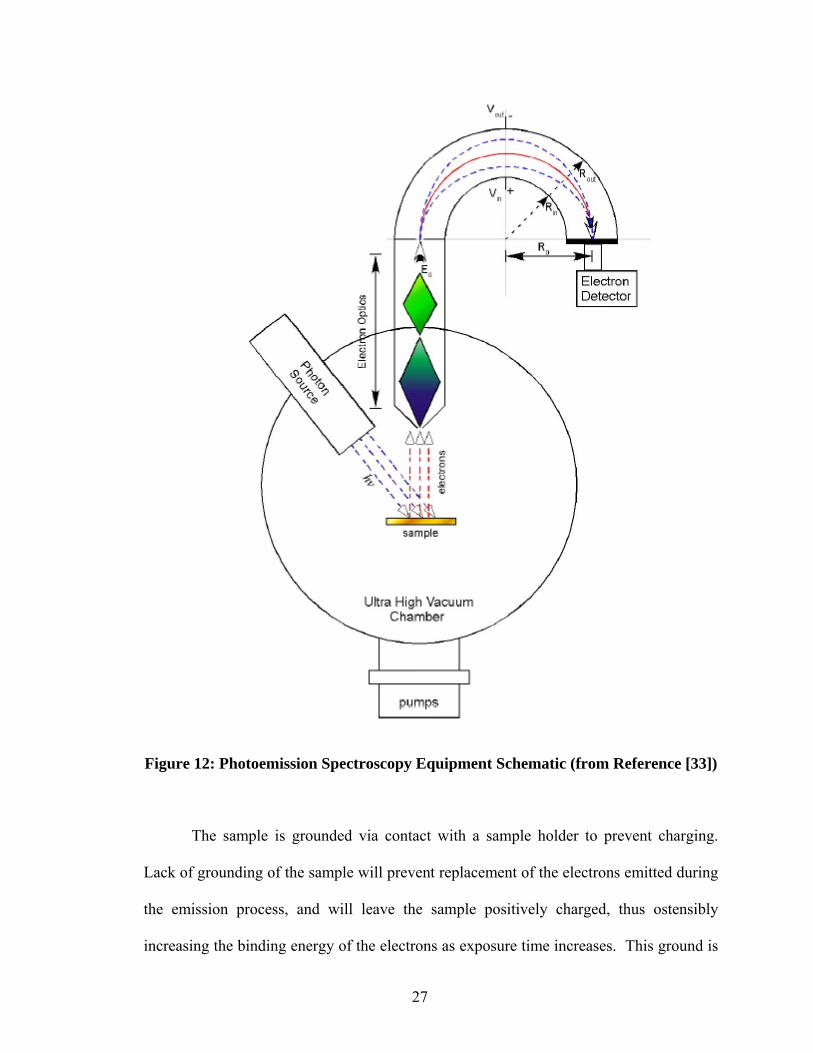
PES Equipment
PES equipment consists of a fixed energy radiation source, a sample, an analyzer,
an electron detector, and a high vacuum environment. The radiation source varies
depending on the type of PES used. Other devices may be used to enhance analysis, such
24
as an electron gun and a voltage generator to bias the sample and improve electron
collection. Figure 12 shows an example schematic of a PES system.
The photon source is typically an X-ray gun for XPS or an ultraviolet (UV) gas
discharge lamp for UPS. The x-rays produced by the x-ray gun in this study came from
Mg (hυ = 1235.6 eV). The UV source produced He I (hυ = 21.22 eV) photons.
The analyzer acts as a band pass filter, allowing only electrons of a certain energy
range through. This is done via tunable magnetic or electrics fields. Those outside the
set range will be deflected and absorbed by the analyzer walls.
The analyzer used in these experiments was a spherical deflection analyzer (SDA).
It consists of two concentric hemispheres, as shown in Figure 12. The analyzer is
arranged to be able to collect the electron released from the sample by the photoelectric
effect. The analyzer is preset to allow the desired electrons in. Before reaching the
analyzer, the electrons must first pass through a physical aperture. This is settable to
different sizes. The smaller the aperture size, the lower the intensity of the electrons that
reaches the analyzer. While the resolution is higher, the aperture is typically set to a low
setting for UPS, due to the high intensity of UV produced by the discharge lamp, which
in turn generates a large number of ionized electrons. A too high intensity of electrons
can damage the analyzer. XPS can be safely used with higher aperture settings.
The electrons must pass another barrier before final entry into the analyzer: the
retardation stage. This retardation is essentially a high pass filter, removing low energy
electrons which tend to increase noise. The retardation energy for the electrons is
constantly adjusted to allow electrons of different energies through and produce a full
spectrum of energy levels.
25
Now the electrons enter the hemispherical analyzer, where they are transported
and filtered via the application of an electric field between the two plates. This voltage is
kept at a user-defined constant to determine the variance of electron energies that are
permitted through, and hence adjusts the resolution of the scan.
An electron detector on the other side of the analyzer then measures the intensity
of the electrons at each energy level. The electron detector used in this study is an
electron multiplier tube, although micro-channel detectors are also common in PES
systems. The electron detector creates a cascade of electrons produced by the initial
electrons exiting the analyzer. This is accomplished by a voltage applied in the detector,
giving the initial electrons additional energy. These electrons strike the detector wall,
creating several more electrons for each initial electron. The process repeats until a
cascade of electrons has been created, which reach the end of the detector and are
measured.
It should be noted that the work function of the sample is not needed to determine
the binding energy of the emitted electrons. Due to a common ground connection, the
Fermi levels of the sample and spectrometer are equilibrated, their equilibration
confirmed via calibration. Thus, the measured electrons have a binding energy given by:
KE = hυ – BE – Φs.
where Φs is the work function of the spectrometer.
The sample is grounded via contact with a sample holder to prevent charging.
Lack of grounding of the sample will prevent replacement of the electrons emitted during
the emission process, and will leave the sample positively charged, thus ostensibly
increasing the binding energy of the electrons as exposure time increases. This ground is
27
also used as a reference level for the Fermi equilibration of the sample and spectrometer,
as described above.
The spectroscopy process is performed in a high vacuum environment to sustain
the integrity of a sample’s surface composition during measurements. A high vacuum
environment will allow the sample to remain contamination-free for up to several days if
the pressure is low enough. By contrast, even a few seconds spent in ambient conditions
will cause the sample to accumulate contaminants on its surface that will significantly
affect the measurements.
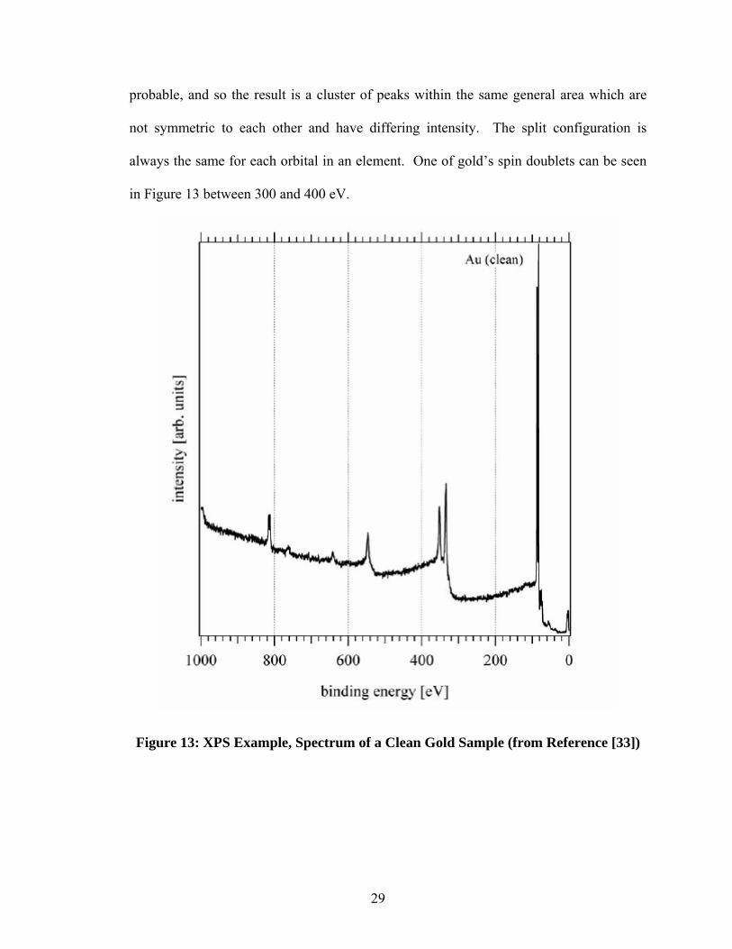
X-ray Photoelectron Spectroscopy
X-rays are ideal for probing the core levels of the molecules in a sample due to
their high energies. Each element contains electrons at characteristic binding energies
that can be measured. Evaluation of the full range of electron energies emitted by the x-
rays allows a detailed spectrum of these characteristic energies, and allows a
determination of which elements are present in the sample, depending on the orbital
peaks present. Given similar ionization cross sections, a higher peak implies a greater
number of the element within the sample. Only electrons with binding energies smaller
than the x-rays’ energy value can be probed, as those with higher binding energies will
not receive enough energy to leave the sample.
Figure 13 shows an example of a cleanly sputtered Au sample characterized by
XPS. The resulting peaks are all characteristic of Au.
Electrons within the same orbital may produce different binding energies,
depending on the configuration of the electrons. These configurations are not equally
28
probable, and so the result is a cluster of peaks within the same general area which are
not symmetric to each other and have differing intensity. The split configuration is
always the same for each orbital in an element. One of gold’s spin doublets can be seen
in Figure 13 between 300 and 400 eV.
Figure 13: XPS Example, Spectrum of a Clean Gold Sample (from Reference [33])
29
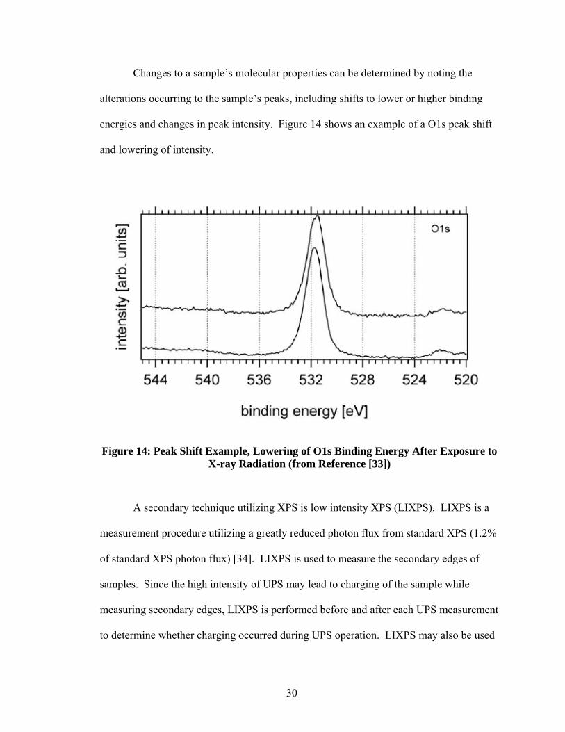
Changes to a sample’s molecular properties can be determined by noting the
alterations occurring to the sample’s peaks, including shifts to lower or higher binding
energies and changes in peak intensity. Figure 14 shows an example of a O1s peak shift
and lowering of intensity.
Figure 14: Peak Shift Example, Lowering of O1s Binding Energy After Exposure to X-ray Radiation (from Reference [33])
A secondary technique utilizing XPS is low intensity XPS (LIXPS). LIXPS is a
measurement procedure utilizing a greatly reduced photon flux from standard XPS (1.2%
of standard XPS photon flux) [34]. LIXPS is used to measure the secondary edges of
samples. Since the high intensity of UPS may lead to charging of the sample while
measuring secondary edges, LIXPS is performed before and after each UPS measurement
to determine whether charging occurred during UPS operation. LIXPS may also be used
30
in lieu of standard UPS on light-sensitive samples, such as ITO. A bias voltage is
typically applied to separate analyzer and sample secondary edges and to collect emitted
electrons more efficiently.
Ultraviolet Photoemission Spectroscopy
Ultraviolet photoemission spectroscopy is used to analyze the valence bands of a
sample and determine its work function through analysis of the secondary edge. The gas
discharge lamp typically used for UPS provides a narrow line width of radiation to the
gas’s discrete energy structure, and also allows a large photon flux, permitting the
process a high resolution and a high ration of signal to noise. He I α is the typical photon
used, with an energy of 21.22 eV. UPS is generally used to investigate such properties as
the highest occupied molecular orbital (HOMO) and charge injection barriers of a sample.
Because of the source of the photons from UPS is a gas, the atoms emit photons in a
narrow band of energies, increasing resolution of the resulting spectra and narrowing the
peak widths. A bias voltage is typically used in conjunction with UPS to increase the
magnitude of the secondary edge and to separate analyzer and sample secondary edges.
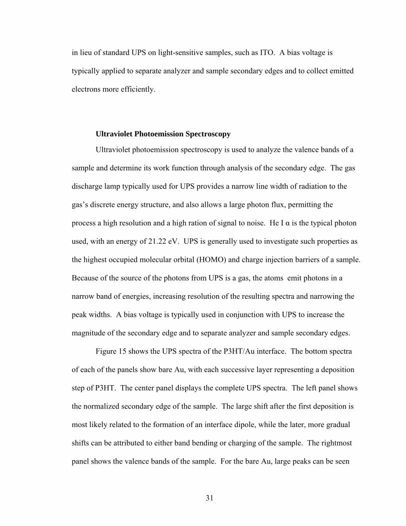
Figure 15 shows the UPS spectra of the P3HT/Au interface. The bottom spectra
of each of the panels show bare Au, with each successive layer representing a deposition
step of P3HT. The center panel displays the complete UPS spectra. The left panel shows
the normalized secondary edge of the sample. The large shift after the first deposition is
most likely related to the formation of an interface dipole, while the later, more gradual
shifts can be attributed to either band bending or charging of the sample. The rightmost
panel shows the valence bands of the sample. For the bare Au, large peaks can be seen
31
which represent the d-bands of the gold. As more P3HT is deposited, these peaks
attenuate and P3HT-related characteristic emission arise.
Figure 15: UPS Spectra of the P3HT/Au Interface
32
Experimental Three main experiments were performed to investigate the electronic properties of
various P3HT interfaces. P3HT was deposited on three substrates: Au, HOPG, and ITO.
The ITO experiment was performed differently from the others due to special
consideration of the ITO substrate. These experiments will be discussed at length in the
following sections, with the ITO experiment explained in detail following the first two.
Experimental Method
All experiments were performed in an ultra high vacuum (UHV) system, shown
in Figure X. The system was composed of four chambers: a fast entry lock, a preparation
chamber, a deposition chamber, and an analysis chamber. The system was acquired from
SPECS (Berlin, Germany). The base pressures of the chambers were 1x10⁻¹⁰ for the
analysis chamber, 1x10⁻⁸ for the preparation chamber, and 1x10⁻⁷ for the entry and
deposition chambers. The system was pumped with turbomolecular/rotary pumps in
combination with ion pumps. The preparation chamber contained a SPECS IQE 11/35
ion source for Ar+ ion sputtering. The analysis chamber was equipped with a SPECS
non-monochromated XR 50 dual x-ray gun for XPS, a SPECS UVS 10/35 ultraviolet
source for UPS, and a SPECS Phoibos 100 hemispherical analyzer. Igor Pro software
(Wavemetrics, Inc.) was used for all evaluation, graphing, and curve fitting.
The P3HT was prepared in a toluene solution at 0.1 mg/ml and kept wrapped in
an aluminum cover to avoid exposure to light. The P3HT had a weight-average
33
molecular weight (Mw) of 19 398 with a polydispersity index (Mw/Mn) of 1.59 as
determined by gel permeation chromatography (GPC) based on polystyrene standards.
100nm thick Au films were created via thermal evaporation on Si wafers. The ITO and
HOPG substrates were purchased from Mikromasch USA (“ZYA” quality), and X,
respectively. A 5 V bias was applied to the samples during UPS and LIXPS to separate
the analyzer and sample secondary edges. Mg Kα (hυ = 1235.6 eV) radiation was used
for the XPS measurements, and He I (hυ = 21.22 eV) for the UPS measurements. The
PES measurements were analyzed via a SPECS Phoibos 100 hemispherical analyzer.
Peaks were fit using a Gauss-Lorentzian profile, as outlined by Kojima and Kurahashi
[35]. Work function and HOMO cutoffs were determined by fitting a line tangent to the
curve of the cutoff and evaluating its intersection with the energy axis of the spectra.
Analyzer broadening was corrected by adding 0.1 eV to the fitted cutoff values.
Sample Preparation
For each experiment, the substrates were sonicated in acetone, iso-propanol, and
methanol, and then dried. The substrates were then mounted onto a sample holder using
conductive silver epoxy. For the Au and ITO samples, a small spot of silver epoxy
provided an electrical contact between the sample and the holder to allow a path to
ground. Once inside the UHV system, the HOPG sample was cleaved to provide a
contamination-free surface.
34
Au and HOPG Analysis Procedure
Each sample was placed into the fast entry load lock. After stabilization of
pressure, the sample was moved to the preparation chamber, where it was sputtered with
Ar+ ions for 30-60 minutes. The sample was then transferred to the analysis chamber.
LIXPS was performed on the sample, followed by UPS and then another LIXPS
investigation. The LIXPS experiments were performed to ensure no charging occurred
during the high intensity UPS investigation. Following this, XPS was performed, first as
a survey scan on the entire energy range available to XPS, and then as intense, focused
investigations on orbital peaks of particular importance to the analysis of the sample and
the eventual P3HT deposition.
After this initial analysis, the sample was transferred to the deposition chamber,
where it was prepped for deposition of P3HT. A laser crosshair was utilized for correct
positioning of the sample.
A syringe filled with P3HT solution was placed onto a syringe pump, where it
was injected into the electrospray chamber through a capillary. The injection rates were
10 ml/h for the Au and HOPG samples and 4 ml/h for the ITO sample. The electrospray
capillary was biased at -3.5 kV relative to the grounded chamber. N2 gas was pumped
into the electrospray enclosure around the orifice to prevent exposure to ambient
contamination.
After initial deposition, the sample was transferred back to the analysis chamber,
where the previous PES steps were again performed. This procedure was performed
several times, with seven depositions of P3HT solution on the Au substrate (for a total of
6.35 ml) and five depositions on the HOPG substrate (for a total of 3.15 ml).
35
ITO Analysis Procedure
It has been observed that high intensity UV and x-rays significantly reduce the
work function of ITO substrates [34, 36]. Due to this limitation, only LIXPS was
performed on the ITO substrate during P3HT deposition. The substrate also was not
sputter cleaned, as this procedure also affects changes in the work function. Upon first
loading and after each deposition, LIXPS was performed on the sample. These were
done as quickly as possible to prevent unnecessary exposure to x-rays. A total of seven
depositions were performed, resulting in a total of 6.45 ml of P3HT solution injected into
the electrospray chamber. After the final LIXPS measurement, UPS was performed to
examine the effects of high intensity UV light on the ITO work function.
To measure the effects of x-ray exposure on ITO, two more ITO substrates were
examined. The first was exposed to LIXPS 24 times, the measurements being performed
as the exposure took place. The second was exposed to high intensity x-rays. Each
exposure time was double the previous one, with the first exposure time set to 30 seconds.
A total of six exposures were performed, with LIXPS performed between each exposure
to evaluate the secondary edge shifts that occurred during exposures.
36
Results and Discussion
P3HT/HOPG Results
Figure 15 shows the S2p core level spectra of the P3HT/HOPG thin film. From
first to last P3HT deposition, the S2p doublet shifts from a starting position of 163.88 eV
to 164.0 eV, a total of 0.12 eV, most likely related to band bending at the interface. The
magnitude of the peak also increases as P3HT is deposited, from the sulfur atom present
inside the chain of a thiophene monomer.
Figure 16 displays the UPS spectra of the P3HT/HOPG junction. The center
panel displays the complete UPS spectra. The rightmost panel shows a normalized close
up of the secondary cutoff. The secondary edge shifts from 16.60 eV (vacuum-cleaved
HOPG) to 16.77 eV, indicating a reduction in the work function 0.17 eV, most likely
related to band bending and a small interface dipole (small due to the stable nature of
HOPG). The rightmost UPS panel shows the valence band spectra of the interface, with
background removed. A transition from HOPG to P3HT-dominant emissions reveals a
weak P3HT HOMO shoulder of 0.41 eV.
37
Figure 16: S2p XPS Core Level Spectra for P3HT/HOPG Interface
38
Figure 17: UPS Spectra for P3HT/HOPG Interface
P3HT/HOPG Discussion
The UPS and XPS data of the P3HT/HOPG interface can be analyzed to construct
an orbital lineup diagram of the junction. The UPS data in Figure 16 show the shift in the
secondary edge as P3HT is deposited. A very gradual shift throughout the deposition
process implies a lack of strong charging and a small or negligible interface dipole. Since
the weak emission of the S 2p peak makes it an unreliable benchmark for band bending,
the secondary edge shift is used to determine the amount of band bending, showing a
shift of 0.17 eV from first to last deposition. This shift includes both band bending and
39
interface dipole, however. The dipole can be estimated by taking the work function of
the pristine HOPG (ΨHOPG = 4.61 eV) and comparing it to the work functions of the first
two depositions, which yielded values of 4.57 and 4.53 eV. This implies an interface
dipole of between 0.04 and 0.08 eV, which when subtracted from the total work function
shift of 0.17 eV yields band bending values of 0.09-0.14 eV. The average of these values
(0.12 eV) is in perfect agreement with the shift of the S 2p peak.
The ionization energy of the P3HT was determined by adding the work function
of the 3.15 ml layer with the HOMO cutoff position (0.41 eV), yielding a value of
4.44 eV + 0.41 eV = 4.85 eV
This is in reasonable agreement with the ionization energy value found in the P3HT/Au
experiment. This value was used for the ionization energy of the P3HT/ITO experiment,
because of the difficulty in evaluating the ionization energy in the ITO experiment.
The hole injection barrier at the interface can be determined by subtracting the
band bending (0.12 eV) from the HOMO cutoff position (0.41 eV), yielding a value of
0.29 eV. The electron injection barrier Φe = 1.41 was determined by subtracting the hole
injection barrier from a previously discovered optical band gap of Eg = 1.7 eV,
determined by UV-visible spectroscopy [X]. This should be taken as a lower limit for the
electron injection barrier, as the optical band gap (by the exciton binding energy) is
smaller than the polaron band gap, which should be used for the band gap. The resulting
data gathered and analyzed was used to construct an orbital lineup diagram of the
interface, Figure 17.
40
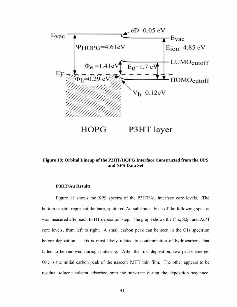
Figure 18: Orbital Lineup of the P3HT/HOPG Interface Constructed from the UPS and XPS Data Set
P3HT/Au Results
Figure 18 shows the XPS spectra of the P3HT/Au interface core levels. The
bottom spectra represent the bare, sputtered Au substrate. Each of the following spectra
was measured after each P3HT deposition step. The graph shows the C1s, S2p, and Au4f
core levels, from left to right. A small carbon peak can be seen in the C1s spectrum
before deposition. This is most likely related to contamination of hydrocarbons that
failed to be removed during sputtering. After the first deposition, two peaks emerge.
One is the initial carbon peak of the nascent P3HT thin film. The other appears to be
residual toluene solvent adsorbed onto the substrate during the deposition sequence.
41
During the last three depositions, the C1s peak shifts to the left 0.11 eV (determined by
peak fitting), which may be an indication of band bending. The S2p and Au4f show
similar shifts. The Au4f peaks also attenuate during deposition as the gold is covered by
the P3HT film.
Figure 19 shows the UPS spectra of the P3HT/Au interface. The central panel
shows the spectra in their entirety. To the left, a normalized close up of the interface
secondary edge is presented. A strong shift is present after the first deposition, which is
most likely related to an electric dipole formed from the compression of the electron
cloud around the metal surface. After this initial jump, a slower shift to the right can be
seen, more likely due to band bending rather than charging because the shift saturates as
more P3HT is deposited. The rightmost panel displays the valence bands spectra. The
sharp peaks visible in the valence band are the Au sample’s d-orbitals. As the P3HT thin
film grows, the Au valence band features attenuate and P3HT HOMO features arise. The
HOMO cutoff of the final P3HT thin film is measured to be 0.7 eV.
42
Figure 19: XPS Core Level Spectra for P3HT/Au Interface
43
Figure 20: UPS Spectra for P3HT/Au Interface
P3HT/Au Discussion
Evaluation of the P3HT/Au photoemission spectroscopy measurements gives us a
detailed look at the electronic properties of the interface. The UPS spectra, shown in
Figure 19, display the work function and the HOMO value of the junction before and
after each deposition. The spectrum of the sputtered Au (bottom spectrum) is
characteristic of Au UPS emissions, with prominent peaks representing the d-bands of the
Au. New features arise on top of the gold peaks as the P3HT is deposited. These
44
features have been related earlier to bonding orbitals of the alkyl ligands (bands >5 eV),
sulfur related localized states (peak at ~3.8 eV), and backbone related localized states
(shoulder at ~1 eV) [37, 38].
After the first deposition, the secondary edge of the interface experiences a strong
shift to the left. This shift is most likely related to an interface dipole, caused by the
electron gas surrounding the metal being pushed into the metal surface by the P3HT
overlayer and thus reducing the metal work function [39].
The XPS spectra shown in Figure 18 show the C1s, S2p, and Au4f peaks of the
interface during P3HT deposition. The bottom C1s spectrum shows a weak signal
present before P3HT deposition, probably related to ambient contamination missed by the
sputter cleaning. After the first deposition (0.15 ml), a two component peak arises, the
lower energy peak corresponding to a small amount of Toluene solvent coadsorbed
during deposition. The P3HT C1s peak continues to strengthen after each deposition, and
shifts slightly during the last three depositions a total of 0.11 eV. This is due to the
occurrence of band bending as the Fermi levels of the polymer layer and substrate
equilibrate. A similar shift is seen for the S2p peak. Charging is ruled out because the
shifting saturates instead of accelerates, and no similar shift is seen in the UP spectra,
where much higher magnitudes of photon intensity are used. No x-ray damage is
presumed because none of the XPS peaks show typical shape degradation after severe x-
ray exposure [40].
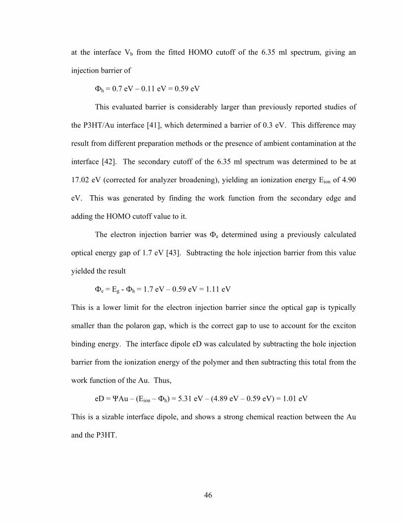
Using the information garnered from the XPS and UPS spectra, an electronic
interface diagram can be constructed. Figure X shows a summary of the evaluation. The
hole injection barrier Фh was determined by subtracting the band bending of the polymer
45
at the interface Vb from the fitted HOMO cutoff of the 6.35 ml spectrum, giving an
injection barrier of
Фh = 0.7 eV – 0.11 eV = 0.59 eV
This evaluated barrier is considerably larger than previously reported studies of
the P3HT/Au interface [41], which determined a barrier of 0.3 eV. This difference may
result from different preparation methods or the presence of ambient contamination at the
interface [42]. The secondary cutoff of the 6.35 ml spectrum was determined to be at
17.02 eV (corrected for analyzer broadening), yielding an ionization energy Eion of 4.90
eV. This was generated by finding the work function from the secondary edge and
adding the HOMO cutoff value to it.
The electron injection barrier was Фe determined using a previously calculated
optical energy gap of 1.7 eV [43]. Subtracting the hole injection barrier from this value
yielded the result
Фe = Eg - Фh = 1.7 eV – 0.59 eV = 1.11 eV
This is a lower limit for the electron injection barrier since the optical gap is typically
smaller than the polaron gap, which is the correct gap to use to account for the exciton
binding energy. The interface dipole eD was calculated by subtracting the hole injection
barrier from the ionization energy of the polymer and then subtracting this total from the
work function of the Au. Thus,
eD = ΨAu – (Eion – Фh) = 5.31 eV – (4.89 eV – 0.59 eV) = 1.01 eV
This is a sizable interface dipole, and shows a strong chemical reaction between the Au
and the P3HT.
46
Comparison of these data with similar oligomer-based thiophene/Au
investigations yields interesting conclusions. A paper by Fujimoto et al. analyzes the
results of HOMO density of state changes with changes in oligomer chain length [44].
Comparison with their UP data on octithiophene bears a close similarity with our
polymer measurements, the primary difference being a more spread out HOMO cutoff on
the polythiophene, suggesting a stronger dispersion of the HOMO band due to its longer
chain length. Chandekar and Whitten [8] have reported an inverse relationship between
the oligothiophene chain length and the hole injection barrier values, i.e. a higher chain
length results in a smaller injection barrier. Their data on the sexithiophene oligomer
show a hole injection barrier of 1.1 eV, significantly larger than the measured 0.7 eV of
the final deposition step in the polymer experiments. They also report an ionization
energy of 5.2 eV, a difference of 0.6 eV from our reported ionization energy. This
suggests a symmetrical increase in their hole and electron barriers from ours.
Another study done by Schwieger et al. [45] reports a more significant difference
between the the oligomer and polymer interfaces structures, reporting a 1.2 eV work
function shift during deposition of a sexithiophene overlayer, suggesting a larger
interface dipole. Their data shows a hole injection barrier of 1 eV, a measurement similar
to the one in reference 8.
47
Figure 21: Orbital Lineup of the P3HT/Au Interface Constructed from the UPS and XPS Data Set
P3HT/ITO Results
Figure 21 shows the results of the ITO work function shifts when exposed to
LIXPS. A total of 24 measurements were performed, in succession and as quickly as
possible to keep the time between measurements consistent. The work function of the
ITO was reduced by 0.18 eV during the course of the experiment.
Figure 22 displays the ITO work function shifts when exposed to standard
intensity x-rays, as measured by LIXPS. Seven measurements were performed, each one
after a period of x-ray exposure double the previous time, beginning with a 30 second
exposure. The leftmost panel shows the shift of the secondary edge caused by the x-ray
exposure, while the right panel shows a graph of x-ray exposure time versus work
48
function of the ITO sample. A total shift of 0.53 eV was observed over the course of the
exposures.
Figure 23 shows the results of LIXPS measurements performed on an ITO sample
upon which P3HT was deposited. A total of seven depositions were performed, between
which LIXPS measurements were carried out. After the final LIXPS measurement, a
UPS measurement was performed. The leftmost panel shows the secondary shift of the
sample as the P3HT was deposited. A total shift of 0.17 eV was detected between the
first and last LIXPS measurement. The UPS measurement reduced the work function an
additional 0.59 eV. The middle panel shows the UPS spectra measured after the final
LIXPS measurement. The rightmost panel shows the HOMO region of the ITO sample
after the final UPS exposure, pinning the HOMO cutoff at 0.81 eV (middle panel inset).
Figure 22: ITO Work Function After Light Intensity X-ray Exposure
49
Figure 23: LIXPS Measurements of ITO Sample After Exposure to Standard Intensity X-rays
50
Figure 24: LIXPS and UPS Spectra for P3HT/ITO Interface
P3HT/ITO Discussion
Given the data on ITO work function alteration from repeated x-ray exposure, it
was determined that LIXPS measurements would not change the work function
significantly. Over the course of 18 consecutive LIXPS measurements, the work function
of the ITO decreased 0.18 eV. Since only eight LIXPS measurements were planned for
the P3HT/ITO experiment, the work function change during the first eight LIXPS
measurements was also recorded. As seen in Figure 21, the alteration in work function
during the first 10 scans is much less than in the subsequent 14, suggesting that reliable
measurements could be obtained if the number of LIXPS scans was kept below 10.
51
A similar experiment to determine the reliability of standard XPS measurements
found a shift of 0.53 eV after only six steps, an unacceptable deviation, and so standard
XPS was ruled out for the measurement of the P3HT/ITO interface. A substantial
deviation in ITO work function caused by a single UPS measurement also ruled out the
use of UPS as a mechanism to further examine the interface, leaving LIXPS as the only
viable option.
Given the data available gathered from LIXPS measurements of the emerging
P3HT overlayer, the orbital band lineup of the interface could be constructed. The
valence band minimum (VBM) and conduction minimum (CBM) needed to be
determined first. We calculated the VBM relative to the Fermi level by using the In 3d5/2
peak located at 445.04 eV, since the VBM could not be determined by valence band
spectra due to superimposed P3HT emissions. The known energy difference between the
X peak and the VBM [15] is 441.8 eV, giving a VBM of 3.24 eV, which is in agreement
with recent results [46]. Using an optical gap of 3.6 eV [15], the CBM was determined to
be 0.36 eV.
We used the previously measured ionization energy from the HOPG experiment
of 4.85 eV for constructing the P3HT/ITO lineup, because of the difficulty in analyzing
the ionization energy from the ITO data. Using this and other data, the interfacial orbital
lineup was constructed, shown in Figure 24. The work function of the sample decreases
0.17 eV from the bare ITO to the last P3HT deposition. This shift probably contains a
LIXPS induced work function reduction of 0.05 eV corresponding to 8 LIXPS scans
(Figure 21). This gives a total of 0.12 eV work function reduction, which is most likely
due to a weak interface dipole eD. Using the P3HT ionization energy and aligning the
52
ITO and P3HT vacuum levels (taking the dipole into account), we determined the HOMO
cutoff of the P3HT layer to be 0.25 eV below the Fermi level. Subtracting the HOMO
cutoff position from the ITO VBM (3.24 eV), a VBM to HOMO offset of 2.99 eV was
determined. The lowest occupied molecular orbital (LUMO) of the P3HT was calculated
to be 1.45 eV above the Fermi level by using the P3HT optical gap of Eg = 1.7 eV as
determined by UV-vis absorption [43]. The ITO CBM to P3HT LUMO distance was
calculated to be Φe = 1.09 eV, a lower estimate since optical band gap measurements
include excitonic features, resulting in generally smaller band gaps than those actually
encountered by charge carriers.
The UPS measurement performed after the final LIXPS measurement further
altered the configuration of the interface, as seen in Figure 24. UV exposure reduced the
ITO work function 0.59 eV, for a total reduction of 3.96 eV. This implies a new interface
dipole eD = 0.76 eV. Band bending is ruled out as an explanation, as earlier
investigations [34] showed no shifts in core levels during XPS core level measurements.
The new HOMO level after UPS measuring was determined to be 0.81 eV (Figure 24,
insert). This implied a new ionization energy of 4.77 eV for the P3HT layer, a small
change from the earlier 4.85 eV [47]. This deviation possibly results from weak charging
artifacts, since small work function areas dominate secondary edge measurements, while
primary peaks represent a true average over all areas of a sample. Figure 24 Shows the
new orbital band lineup diagram after UV exposure. The larger interface dipole shifted
the features of the interface down to approximately 0.6 eV lower binding energies.
53
Figure 25: Orbital Lineup of the P3HT/ITO Interface Before and After UPS Exposure
54
Conclusion
P3HT/Au
In this experiment P3HT was deposited onto a clean Au surface in several steps,
with x-ray and ultraviolet photoemission spectroscopy performed between each step. The
measurements were performed in situ in an ultra high vacuum environment. Once a
suitable layer of P3HT was grown, the data were analyzed using Igor Pro software and an
orbital band lineup diagram was created. Several of the properties of the interface were
measured, including the HOMO, charge injection barriers, and the presence of absence of
interface dipoles. The P3HT interface was found to have slightly modified electronic
properties from similar oligomeric interfaces.
P3HT/HOPG
In this experiment P3HT was deposited onto a cleaved HOPG surface in several
steps, with x-ray and ultraviolet photoemission spectroscopy performed between each
step. The measurements were performed in situ in an ultra high vacuum environment.
Once a suitable layer of P3HT was grown, the data were analyzed using Igor Pro
software and an orbital band lineup diagram was created. Several of the properties of the
interface were measured, including the HOMO, charge injection barriers, and the
presence of absence of interface dipoles.
55
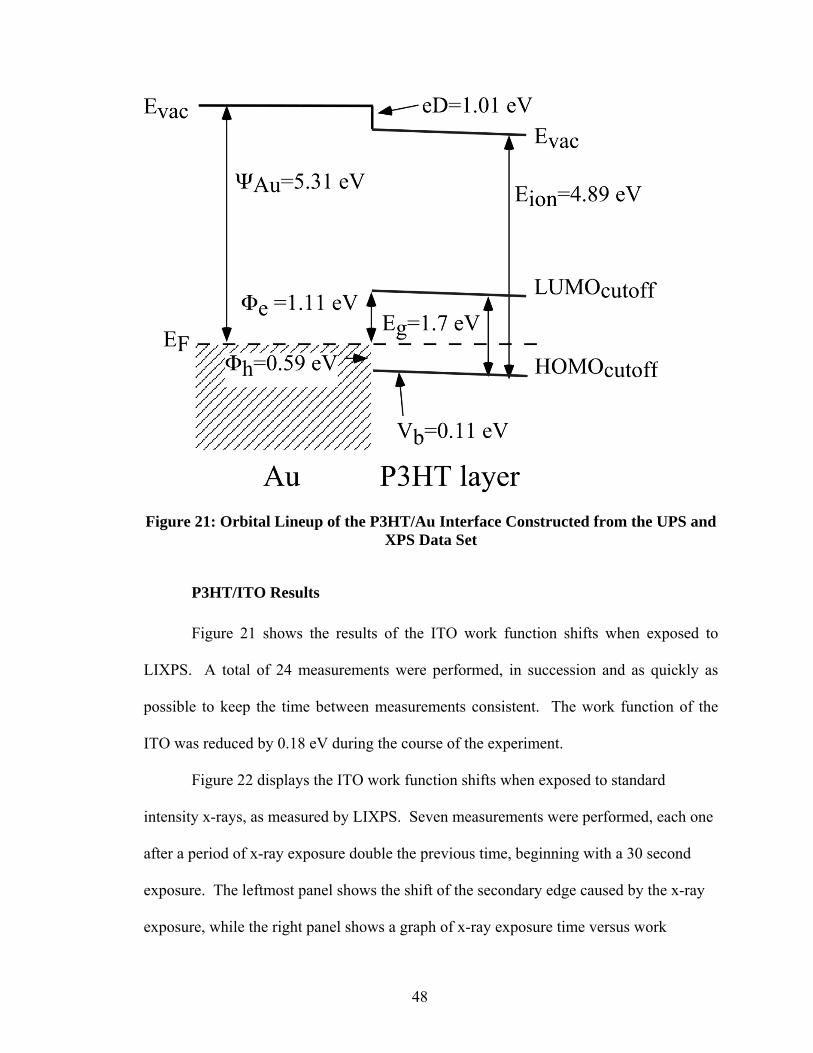
P3HT/ITO
In this experiment bare ITO was exposed to light and standard intensity x-rays to
determine their effect on the ITO’s work function. P3HT was deposited onto a second
ITO substrate in several steps, with light intensity x-ray spectroscopy performed between
each step. The measurements were performed in situ in an ultra high vacuum
environment. Once a suitable layer of P3HT was grown, the data were analyzed using
Igor Pro software and an orbital band lineup diagram was created. Several of the
properties of the interface were measured, including the HOMO, charge injection barriers,
and the presence of absence of interface dipoles.
56
References 1. Huynh, W.U., J.J. Dittmer, and A.P. Alivisatos, Hybrid Nanorod-Polymer Solar
Cells. 2002. p. 2425-2427. 2. Hoppe, H. and N.S. Sariciftci, Organic solar cells: An overview. Journal of
Materials Research, 2004. 19(7): p. 1924-1945. 3. Stutzmann, N., R.H. Friend, and H. Sirringhaus, Self-Aligned, Vertical-Channel,
Polymer Field-Effect Transistors. 2003. p. 1881-1884. 4. Tanase, C., et al., Unification of the Hole Transport in Polymeric Field-Effect
Transistors and Light-Emitting Diodes. Physical Review Letters, 2003. 91(21): p. 216601.
5. Waldrop, J.R. and R.W. Grant, Semiconductor Heterojunction Interfaces:
Nontransitivity of Energy-band Discontiuities. Physical Review Letters, 1979. 43(22): p. 1686.
6. Salaneck, W.R., et al., The electronic structure of polymer-metal interfaces
studied by ultraviolet photoelectron spectroscopy. Materials Science & Engineering R-Reports, 2001. 34(3): p. 121-146.
7. Atreya, M., et al., In situ x-ray photoelectron spectroscopy studies of interactions
of evaporated metals with Poly(p-phenylene vinylene) and its ring-substituted derivatives. 1999, AVS. p. 853-861.
8. Chandekar, A. and J.E. Whitten, Ultraviolet photoemission and electron loss
spectroscopy of oligothiophene films. Synthetic Metals, 2005. 150(3): p. 259-264. 9. Fujimoto, H., et al., Ultraviolet photoemission study of oligothiophenes: pi-band
evolution and geometries. 1990, AIP. p. 4077-4092. 10. Cascio, A.J., et al., Investigation of a polythiophene interface using photoemission
spectroscopy in combination with electrospray thin-film deposition. 2006, AIP. p. 062104.
11. Lyon, J.E., et al., Photoemission study of the poly(3-hexylthiophene)/Au interface.
2006, AIP. p. 222109.
57
12. Yi, Y., et al., Characterization of indium tin oxide surfaces and interfaces using low intensity x-ray photoemission spectroscopy. 2006, AIP. p. 093719.
13. Kasap, S.O., Principles of Electronic Materials and Devices. 2002. 14. Ishii, H., et al., Energy level alignment and interfacial electronic structures at
organic/metal and organic/organic interfaces (vol 11, pg 605, 1999). Advanced Materials, 1999. 11(12): p. 972-972.
15. Gassenbauer, Y. and A. Klein, Electronic surface properties of rf-magnetron
sputtered In2O3 : Sn. Solid State Ionics, 2004. 173(1-4): p. 141-145. 16. Roncali, J., Conjugated Poly(Thiophenes) - Synthesis, Functionalization, and
Applications. Chemical Reviews, 1992. 92(4): p. 711-738. 17. Bokman, F., Analytical Aspects of Atmospheric Pressure Ionization in Mass
Spectrometry. 2002. 18. Gilbert, W., De Magnete. 1600, Londini. 19. Bose, G.M., Recherches Sur La Cause Et Sur La Veritable Theorie De
L'Electricite. 1745, Wittembergae. 20. Nollet, J.A., Recherches Sur Les Causes Particulieres Des Phenomenes
Electrique. 1753, Paris. 21. Taylor, G.I., Proceedings of the Royal Society in London A A280. 22. Whitehouse, C.M., et al., Electrospray Interface for Liquid Chromatographs and
Mass Spectrometers. Analytical Chemistry, 1985. 57(3): p. 675-679. 23. Yamashita, M. and J.B. Fenn, Electrospray Ion-Source - Another Variation on the
Free-Jet Theme. Journal of Physical Chemistry, 1984. 88(20): p. 4451-4459. 24. Alexandrov, M.L., et al., Ion Extraction from Solutions at Atmospheric-Pressure -
a Method of Mass-Spectrometric Analysis of Bioorganic Substances. Doklady Akademii Nauk Sssr, 1984. 277(2): p. 379-383.
25. Bruins, A.P., T.R. Covey, and J.D. Henion, Ion Spray Interface for Combined
26. Wong, S.F., C.K. Meng, and J.B. Fenn, Multiple Charging in Electrospray
Ionization of Poly(Ethylene Glycols). Journal of Physical Chemistry, 1988. 92(2): p. 546-550.
58
27. Wilm, M. and M. Mann, Analytical properties of the nanoelectrospray ion source. Analytical Chemistry, 1996. 68(1): p. 1-8.
28. Smith, D.P.H., The Electrohydrodynamic Atomization of Liquids. Ieee
Transactions on Industry Applications, 1986. 22(3): p. 527-535. 29. Dole, M., L.L. Mack, and R.L. Hines, Molecular Beams of Macroions. Journal of
Chemical Physics, 1968. 49(5): p. 2240-&. 30. Thomson, B.A. and J.V. Iribarne, Field-Induced Ion Evaporation from Liquid
Surfaces at Atmospheric-Pressure. Journal of Chemical Physics, 1979. 71(11): p. 4451-4463.
31. Einstein, A., Generation and conversion of light with regard to a heuristic point
of view. Annalen Der Physik, 1905. 17(6): p. 132-148. 32. Hufner, S. 2003. 33. Gargagliano, Characterization of L-cysteine Thin Films Via Photoemission
Spectroscopy. 2005: Tampa. 34. Beerbom, M.M., et al., Direct comparison of photoemission spectroscopy and in
situ Kelvin probe work function measurements on indium tin oxide films. Journal of Electron Spectroscopy and Related Phenomena, 2006. 152(1-2): p. 12-17.
35. Kojima, I. and M. Kurahashi, Application of Asymmetrical Gaussian Lorentzian
Mixed-Function for X-Ray Photoelectron Curve Synthesis. Journal of Electron Spectroscopy and Related Phenomena, 1987. 42(2): p. 177-181.
36. Schlaf, R., H. Murata, and Z.H. Kafafi, Work function measurements on indium
tin oxide films. Journal of Electron Spectroscopy and Related Phenomena, 2001. 120(1-3): p. 149-154.
37. Dannetun, P., et al., The Chemical and Electronic-Structure of the Interface
between Aluminum and Polythiophene Semiconductors. Journal of Chemical Physics, 1993. 99(1): p. 664-672.
38. Salaneck, W.R., et al., Thermochromism in Poly(3-Hexylthiophene) in the Solid-
State - a Spectroscopic Study of Temperature-Dependent Conformational Defects. Journal of Chemical Physics, 1988. 89(8): p. 4613-4619.
39. Knupfer, M. and G. Paasch, Origin of the interface dipole at interfaces between
undoped organic semiconductors and metals. Journal of Vacuum Science & Technology A, 2005. 23(4): p. 1072-1077.
59
40. Nambu, A., et al., Film growth and X-ray induced chemical reactions of thiophene adsorbed on Au(111). Surface Science, 2003. 530(1-2): p. 101-110.
41. Burgi, L., et al., Close look at charge carrier injection in polymer field-effect
transistors. Journal of Applied Physics, 2003. 94(9): p. 6129-6137. 42. Wan, A., et al., Impact of electrode contamination on the alpha-NPD/Au hole
injection barrier. Organic Electronics, 2005. 6(1): p. 47-54. 43. Chen, T.A., X.M. Wu, and R.D. Rieke, Regiocontrolled Synthesis of Poly(3-
Alkylthiophenes) Mediated by Rieke Zinc - Their Characterization and Solid-State Properties. Journal of the American Chemical Society, 1995. 117(1): p. 233-244.
44. Fujimoto, H., et al., Ultraviolet Photoemission-Study of Oligothiophenes - Pi-
Band Evolution and Geometries. Journal of Chemical Physics, 1990. 92(7): p. 4077-4092.
45. Schwieger, T., et al., Electronic properties of interfaces between different
sexithiophenes and gold. Journal of Applied Physics, 2005. 97(12). 46. Lagel, B., et al., Investigation of the poly[2-methoxy-5-(2 '-ethyl-hexyloxy)-1,4-
phenylene vinylene]/indium tin oxide interface using photoemission spectroscopy. Journal of Applied Physics, 2005. 98(2).
47. Lyon, J.E., et al., Photoemission study of the poly(3-hexylthiophene)/Au interface.