+ All Categories
Home > Documents > Fabrication and characterization of a germanium nanowire ...

Fabrication and characterization of a germanium nanowire ...

Date post: 24-Jan-2022
Category:
Upload: others
View: 2 times
Download: 0 times
Share this document with a friend
21
HAL Id: cea-01988258 https://hal-cea.archives-ouvertes.fr/cea-01988258 Submitted on 21 Jan 2019 HAL is a multi-disciplinary open access archive for the deposit and dissemination of sci- entific research documents, whether they are pub- lished or not. The documents may come from teaching and research institutions in France or abroad, or from public or private research centers. L’archive ouverte pluridisciplinaire HAL, est destinée au dépôt et à la diffusion de documents scientifiques de niveau recherche, publiés ou non, émanant des établissements d’enseignement et de recherche français ou étrangers, des laboratoires publics ou privés. Fabrication and characterization of a germanium nanowire light emitting diode Johannes Greil, Emmerich Bertagnolli, Bassem Salem, Thierry Baron, Pascal Gentile, Alois Lugstein To cite this version: Johannes Greil, Emmerich Bertagnolli, Bassem Salem, Thierry Baron, Pascal Gentile, et al.. Fabri- cation and characterization of a germanium nanowire light emitting diode. Applied Physics Letters, American Institute of Physics, 2017, 111 (23), pp.233103. 10.1063/1.5006152. cea-01988258
Transcript

HAL Id: cea-01988258https://hal-cea.archives-ouvertes.fr/cea-01988258

Submitted on 21 Jan 2019

HAL is a multi-disciplinary open accessarchive for the deposit and dissemination of sci-entific research documents, whether they are pub-lished or not. The documents may come fromteaching and research institutions in France orabroad, or from public or private research centers.

L’archive ouverte pluridisciplinaire HAL, estdestinée au dépôt et à la diffusion de documentsscientifiques de niveau recherche, publiés ou non,émanant des établissements d’enseignement et derecherche français ou étrangers, des laboratoirespublics ou privés.

Fabrication and characterization of a germaniumnanowire light emitting diode

Johannes Greil, Emmerich Bertagnolli, Bassem Salem, Thierry Baron, PascalGentile, Alois Lugstein

To cite this version:Johannes Greil, Emmerich Bertagnolli, Bassem Salem, Thierry Baron, Pascal Gentile, et al.. Fabri-cation and characterization of a germanium nanowire light emitting diode. Applied Physics Letters,American Institute of Physics, 2017, 111 (23), pp.233103. 10.1063/1.5006152. cea-01988258

1Corresponding author. Email: [email protected]

Fabrication and characterization of a

germanium nanowire light emitting diode

Johannes Greil1, Emmerich Bertagnolli1, Bassem Salem2,3, Thierry Baron2,3, Pascal

Gentile4, Alois Lugstein1*

1 Institute of Solid State Electronics, TU Wien, Floragasse 7, 1040 Vienna, Austria

2 Université de Grenoble Alpes, LTM, F-38000 Grenoble, France

3 CNRS, LTM, F-38000 Grenoble, France

4 CEA, INAC-PhELIQS, 17 rue des Martyrs, F-38000 Grenoble, France

Abstract

In this letter we demonstrate the feasibility of a germanium nanowire light emitting diode

as a reasonable approach for downscaling of CMOS compatible light sources. We show

room-temperature direct bandgap electroluminescence from axial p-n junction nanowire

devices. The electron population in the Γ valley, necessary for direct bandgap emission,

is achieved by high injection current densities. Carrier temperature is consistently found

to be higher than the lattice temperature, indicating inhibited carrier cooling in small

diameter wires. Strong polarization of the emission parallel to the nanowire axis is

observed and attributed to dielectric contrast phenomena.

2

Main text

The ongoing scaling of CMOS technology and thus conceivable limitations of common

metallization schemes, demands for silicon-compatible light sources, transmitters and

detectors for on-chip communication and triggered enormous research activities in group

IV semiconductor photonics.1,2 Thereby novel light generation schemes like Raman

lasers3, photonic crystals4, quantum dots5, and erbium doping6 have already been

demonstrated. From the material side germanium (Ge) is highlighted amongst the group

IV materials due to its quasidirect nature with the conduction band minimum at the Γ-point

only 140meV higher in energy than the minimum at the L-point. Beneficially, the direct

bandgap energy of Ge translates to an emission wavelength in the telecommunication

band of 1550nm. Moreover, it has already been demonstrated that the emission

properties of Ge may be tailored by utilizing quantum confinement7, strain engineering8,9,

n-type doping10, alloying with Sn11, tuning of the temperature12 or combinations thereof.

Planar Ge LEDs12–16 as well as optically10 and electrically17 pumped Ge lasers have

recently been demonstrated in devices with dimensions on the micron scale. Following

the route of downscaling, nanowire (NW) based devices are a next logical step. However,

so far only III-V materials have been employed in axial p-n junction LED devices18–21. Here

we present room temperature electroluminescence (EL) from Ge NW axial p-n diodes

with a junction area of less than 0.01µm2. A bottom-up approach is pursued, with the

potential for versatile integration of NW functional building blocks in various device

architectures.

3

Ge NWs were synthesized in a low pressure chemical vapor deposition chamber with

GeH4 (50sccm of 10% GeH4 in H2 ) as a precursor gas at a growth temperature of T=673K

and a total chamber pressure of 12.8mbar. The vapor-liquid-solid growth mechanism22

was employed to achieve axial p-n junction NWs with Au colloids as growth catalyzing

particles. The p- and n-type segments are defined by introducing B2H6 (B2H6/GeH4 ratio

= 2x10⁻²) and PH3 (PH3/GeH4 ratio = 3x10⁻²) into the growth chamber, respectively

resulting in electrically active doping densities of about 1019at.cm-3 determined by four

probe measurements.

Uncatalytic deposition on the NW sidewalls during the growth at this rather high

temperature leads to strongly tapered NWs enabling efficient outcoupling of light.23

However, the unintentional deposition of n-type material on the sidewalls of the foremost

grown p-type section of the NW, potentially bypasses the p-n junction electrically24 (see

Figure 1a). Remarkably, as will be shown later, selective etching of this unintentional n-

type layer greatly improves the electrical diode properties, whereas the optical emission

properties are not altered significantly. To fabricate devices as shown in the SEM image

in Figure 1a, the p-n junction NWs were removed from the growth substrate and deposited

via mechanical transfer on a highly doped substrate covered by silicon oxide. Electrical

contacts to individual NWs were established by electron beam lithography, Ni/Au sputter

deposition and lift-off techniques. In agreement with literature we observed ohmic

contacts to both highly doped p- and n-type Ge segments.25

4

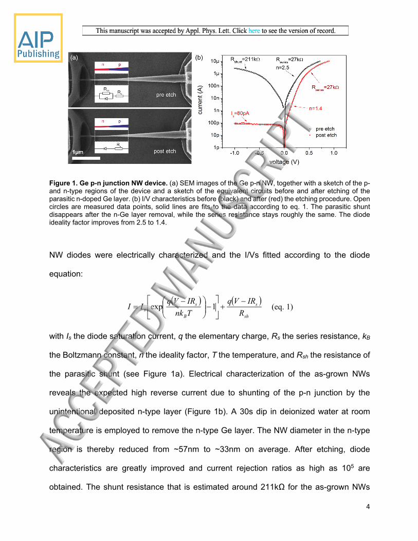
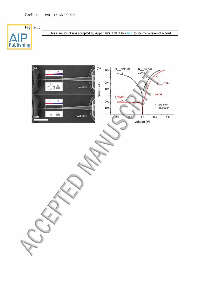
Figure 1. Ge p-n junction NW device. (a) SEM images of the Ge p-n NW, together with a sketch of the p- and n-type regions of the device and a sketch of the equivalent circuits before and after etching of the parasitic n-doped Ge layer. (b) I/V characteristics before (black) and after (red) the etching procedure. Open circles are measured data points, solid lines are fits to the data according to eq. 1. The parasitic shunt disappears after the n-Ge layer removal, while the series resistance stays roughly the same. The diode ideality factor improves from 2.5 to 1.4.

NW diodes were electrically characterized and the I/Vs fitted according to the diode

equation:

sh

s

B

ss R

IRVq

Tnk

IRVqII

1exp (eq. 1)

with Is the diode saturation current, q the elementary charge, Rs the series resistance, kB

the Boltzmann constant, n the ideality factor, T the temperature, and Rsh the resistance of

the parasitic shunt (see Figure 1a). Electrical characterization of the as-grown NWs

reveals the expected high reverse current due to shunting of the p-n junction by the

unintentional deposited n-type layer (Figure 1b). A 30s dip in deionized water at room

temperature is employed to remove the n-type Ge layer. The NW diameter in the n-type

region is thereby reduced from ~57nm to ~33nm on average. After etching, diode

characteristics are greatly improved and current rejection ratios as high as 105 are

obtained. The shunt resistance that is estimated around 211kΩ for the as-grown NWs

5

completely disappears, while the series resistance of around 27kΩ is not affected and the

diode ideality factor improves from n=2.5 to n=1.4.

To gain further insight into the internal electric field distribution along the axial p-n NW

junction, scanning photocurrent spectroscopy was employed (Figure 2).26 Therefore the

short-circuit current of the Ge NW device was recorded while a focused laser beam was

scanned along the NW.

For NWs under certain constraints discussed by Allen et al.27 the photocurrent Iph is

expected to be proportional to the local electric field. Assuming further that the absorption

strength along the tapered NWs is constant, the effective electrostatic potential profile Φeff

along the NW can be determined according to

dxxI pheff )( (eq. 2)

Independent of the excitation power Pexc, the position of the p-n junction is clearly

determined in the electrostatic potential profile, while the potential in the vicinity of the (left)

p-type contact is completely flat. Close to the (right) n-type contact there are indications

of a Schottky barrier induced field, though negligible compared to the p-n junction related

field.

6

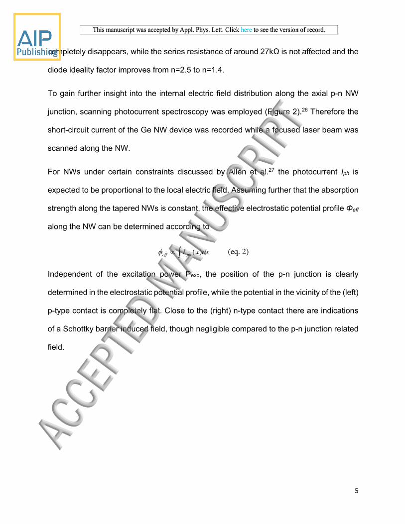
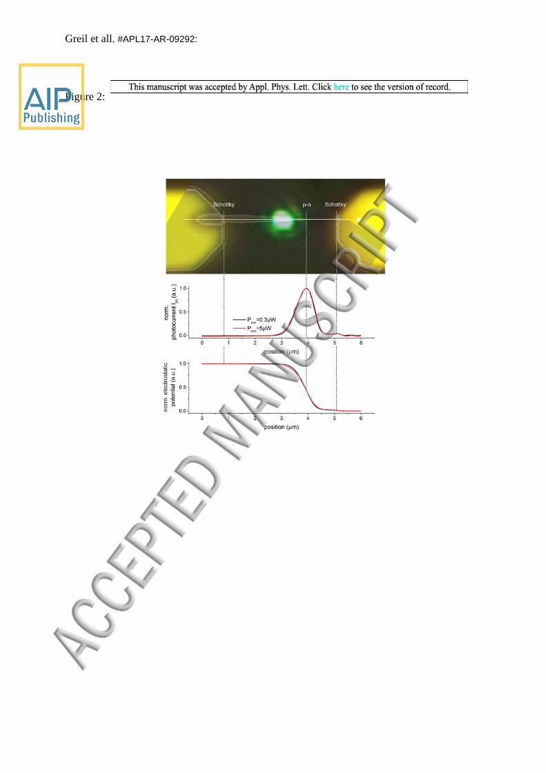
Figure 2. Scanning photocurrent spectroscopy. The uppermost panel shows an overlay of an optical image with the excitation laser spot and an SEM image of the etched NW. Independent of the excitation power, the photocurrent scales with the internal electric field and is highest at the p-n junction, linescans along the NW axis provide the exact position of the junction. The electrostatic potential profile reveals negligible Schottky barriers at the metal-semiconductor contacts. The lowermost panel shows the thereof calculated profile of the effective electrostatic potential.

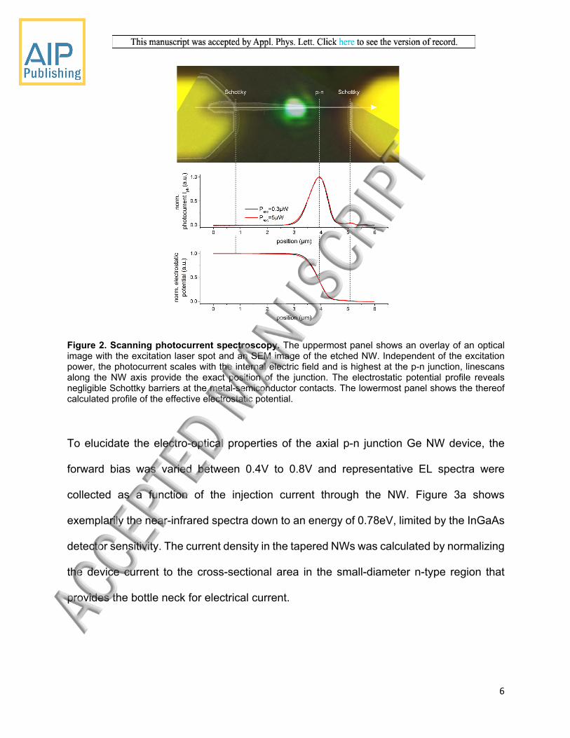
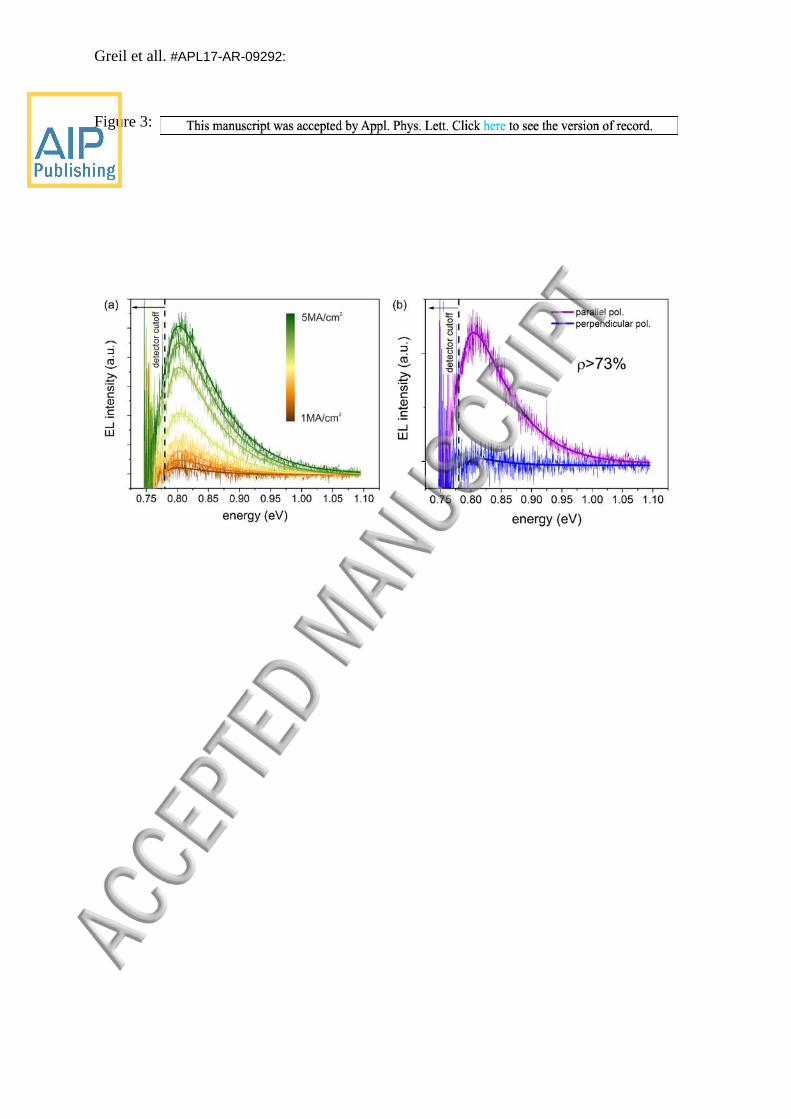
To elucidate the electro-optical properties of the axial p-n junction Ge NW device, the

forward bias was varied between 0.4V to 0.8V and representative EL spectra were

collected as a function of the injection current through the NW. Figure 3a shows

exemplarily the near-infrared spectra down to an energy of 0.78eV, limited by the InGaAs

detector sensitivity. The current density in the tapered NWs was calculated by normalizing

the device current to the cross-sectional area in the small-diameter n-type region that

provides the bottle neck for electrical current.

7

Figure 3. Room temperature EL of the Ge NW p-n diode biased in forward direction. (a) EL spectra for increasing current density, (b) Polarization dependence of the emission. A high degree of polarization >73% was found. Solid lines in both panels are fits to the Maxwell-Boltzmann distribution.

Due to the limitations in detector range we can only observe the direct bandgap transition,

expected at ~0.8eV at room temperature28. The spectra are fitted according to the

Maxwell-Boltzmann distribution29 for spontaneous direct bandgap recombination:

CB

dgdgEL Tk

EhEhI ,

, exp

(eq. 3)

with h Planck’s constant, ν the optical frequency, Eg,d the direct bandgap of Ge and TC the

carrier temperature. Furthermore, the polarization properties of the emission are plotted

in Figure 3b. Strong polarization of the EL is observed along the NW axis with a degree

of polarization of about ρ>73%. A high degree of polarization along the NW axis is

frequently reported for cubic semiconductors30,31 and can be understood in terms of the

dielectric contrast of the NW and its surroundings.32 For an electric field polarized parallel

8

to the Ge NW, the field Ei inside the NW equals the field Ee outside (Ei = Ee). For

perpendicular polarization, though, the field inside is highly attenuated:

ei EE0

02

(eq. 4)

with the dielectric constant for Ge of ε=16.2 and the dielectric constant of air ε0=1. A

theoretical polarization ratio of ρ=97% is expected, even higher than what is

experimentally observed. Additionally, leaky-mode resonances confining light within sub-

wavelength nanostructures exhibit a steep diameter dependency of the TM/TE

polarization ratio.33 Due to the tapering of the p-n NW devices, however, a complex mode

profile may be expected and thus the degree of polarization is not predictable in a straight

forward way.

The EL emission properties were investigated of as grown NWs as well as after the

removal of the parasitic n-doped shell. Figure 4 shows parameters extracted from fits to

the spectra according to eq. 3 before and after the etching procedure. The lattice

temperature is estimated employing two independent approaches. First, temperature is

extracted by employing Varshnis’s law and the bandgap energy Eg,d:

T

TEE dg

2

0, (eq. 5)

with E0=0.89eV the bandgap at T=0K, α=5.82*10-4eV/K2, β=296K.28 Second, Raman

characterization of the NW junction region is employed and we estimate the lattice

9

temperature via the Raman shift of the main optical phonon peak34,35 according to the

linearization kT with ∆T the temperature and ∆Ω the Raman peak shift. The linear

factor k=62.3K/rel.cm-1 was determined from a temperature dependent study.34 The

temperature of the charge carrier was extracted by fitting the high-energy wing of the

electroluminescence spectra.36 The lattice temperature estimated from Raman

characterization appeared to be slightly lower than the lattice temperature estimated from

the temperature dependency of the bandgap energy. We can speculate that locally within

the recombination region the temperature is higher than derived from Raman

characterization at the junction position. In these hot-spots recombination probability is

higher and thus the emission from localized regions with increased temperature could

dominate the emission. Considering the lattice temperature from both approaches, Joule

heating is slightly increasing the temperature of the lattice with increasing current density.

However in this temperature regime we can exclude thermal radiation as a source of

emission in the considered range. The peak wavelength and total radiated amount of a

thermal emitter vary with temperature according to Wien's displacement law. Emission

with a maximum at about 1.5m corresponds thus to a temperature of about 1200K, far

above the temperature we determined for our light emitting device and even above the

melting temperature of Ge.

Overall for all devices we observe a significantly higher carrier temperature of ≈550K as

compared to the lattice temperature of ≈350K at high injection current, indicating non-

equilibrium hot-carrier recombination. Similar to the observed behavior, carrier

temperature has been frequently reported to be higher than the actual junction

temperature in common planar LED structures.36 Proposed mechanisms are Auger

10

recombination, intervalence band absorption37 or high-energy carrier injection in the

active region under large forward bias38. Particularly for NWs, a recent work of Tedeschi

et al.39 has addressed the role of inhibited phonon emission in confined nanostructures

for hot-carrier luminescence. Therein, a general trend of increasing carrier temperature

with decreasing NW diameter was found under quasi-equilibrium conditions provided by

continuous wave excitation. The proposed mechanism relates to effective phonon

scattering at the NW surface, preventing the carriers from reaching thermal equilibrium

with the lattice via phonon emission. Qualitatively this trend is reproduced in Figure 4b,

since the etched NWs tend to exhibit a higher carrier temperature than the as-grown NWs

with larger diameter.

11

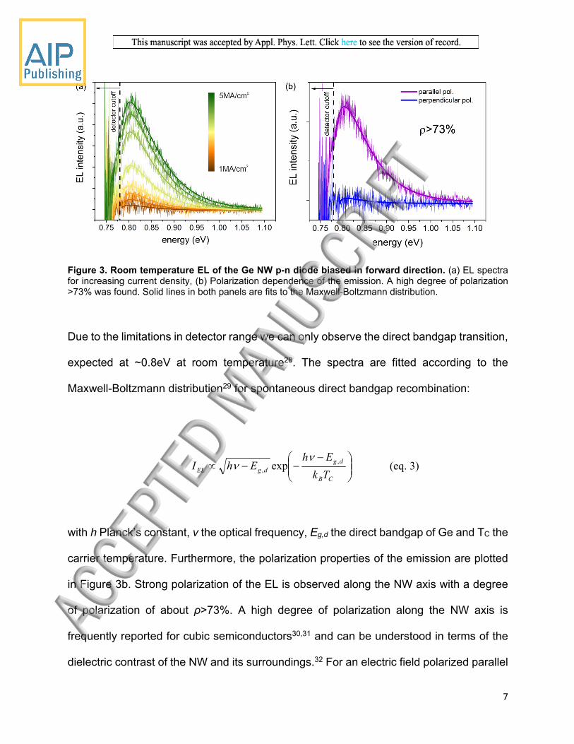
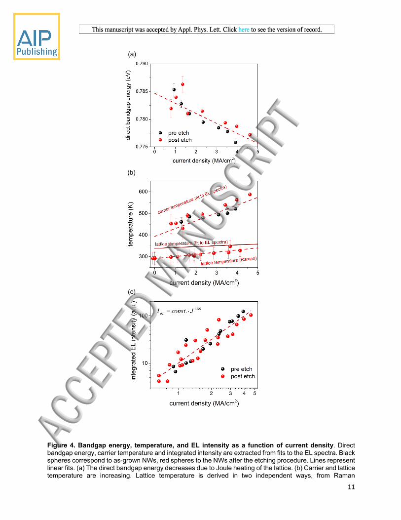
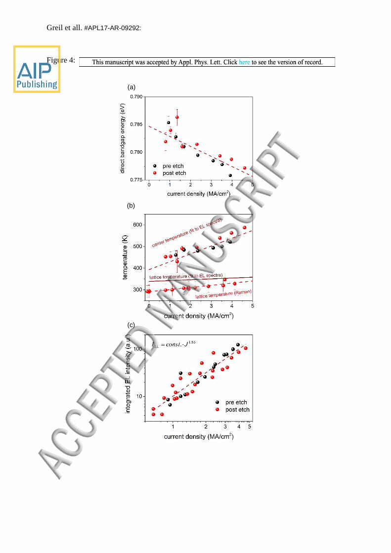
Figure 4. Bandgap energy, temperature, and EL intensity as a function of current density. Direct bandgap energy, carrier temperature and integrated intensity are extracted from fits to the EL spectra. Black spheres correspond to as-grown NWs, red spheres to the NWs after the etching procedure. Lines represent linear fits. (a) The direct bandgap energy decreases due to Joule heating of the lattice. (b) Carrier and lattice temperature are increasing. Lattice temperature is derived in two independent ways, from Raman

(a)

(b)

(c)

12

characterization and from the bandgap values shown in (a) using Varshni’s equation. (c) Integrated EL intensity as a function of current density on a log-log scale follows a power law with exponent k=1.65.

Figure 4c shows the integrated EL intensity as a function of current density. The linear

relationship in the log-log plot indicates a power law kEL JI with the exponent k=1.65.

The intensity dependence compares well with published values of planar Ge LEDs

ranging from k=1.48 - 2. 15,40,41 A superlinear increase of EL intensity with current density

has been proposed to be related to an increased efficiency of the direct bandgap transition

due to (i) an increased ratio of direct to indirect states with high injection41, (ii) Joule

heating15 and (iii) band-filling of the L valley14. At increased temperatures the Fermi

distribution widens and at higher injection the electron quasi Fermi level rises, thus

increasing the density of electrons populating the Γ valley.

Summarizing, we have presented direct bandgap emission from electrically pumped Ge

NW p-n diodes. The EL is dominated by hot-carrier recombination, supposedly due to

inhibited phonon emission in smaller diameter NWs. A superlinear dependency of the EL

intensity on current density is in agreement with previously published data for planar Ge

LEDs. The realized downscaling of a CMOS compatible light source to the nanoscale

could be of great relevance for envisaged on-chip group IV photonics applications.

Acknowledgements

The authors gratefully acknowledge financial support by the Austrian Science Fund

(FWF): project No.: P28175-N27. The authors further thank the Center for Micro- and

Nanostructures for providing the cleanroom facilities.

13

References

(1) R. Geiger, T. Zabel, H. Sigg, Front. Mater. 2, 52.(2015)

(2) L. Tsybeskov, D. J. Lockwood, Proc. IEEE 97, 7, 1284 (2009)

(3) H. Rong, A. Liu, R. Jones, O. Cohen, D. Hak, R. Nicolaescu, A. Fang, M. Paniccia, Nature

433, 292 (2005)

(4) X. Checoury, M. El Kurdi, Z. Han, P. Boucaud, Opt. Express 17, 5, 3500 (2009)

(5) L. Pavesi, L. Dal Negro, C. Mazzoleni, G. Franzò, F. Priolo, Nature 408, 440 (2000)

(6) L. Dal Negro, R. Li, J. Warga, S. N. Basu, Appl. Phys. Lett. 92, 181105 (2008)

(7) J. Xia, T. Maruizumi, Y. Shiraki, Front. Optoelectron. 5, 1, 13 (2012)

(8) M. El Kurdi, G. Fishman, S. Sauvage, P. Boucaud, J. Appl. Phys. 107, 013710 (2010)

(9) M. J. Süess, R. Geiger, R. A. Minamisawa, G. Schiefler, J. Frigerio, D. Chrastina, G. Isella,

R. Spolenak, J. Faist, H. Sigg, Nat. Photonics 7, 466 (2013)

(10) J. Liu, X. Sun, R. Camacho-Aguilera, L. C. Kimerling, J. Michel, Opt. Lett. 35, 5, 679 (2010)

(11) S. Wirths, Z. Ikonic, A.T. Tiedemann, B. Holländer, T. Stoica, G. Mussler, U. Breuer, J.M.

Hartmann, A. Benedetti, S. Chiussi, D. Grützmacher, S. Mantl, D. Buca, Appl. Phys. Lett.

103, 192110 (2013)

(12) T.-H. Cheng, C.-Y. Ko, C.-Y. Chen, K.-L. Peng, G.-L. Luo, C. W. Liu, H.-H. Tseng, Appl.

Phys. Lett. 96, 9, 091105 (2010)

(13) W. Hu, B. Cheng, C. Xue, H. Xue, S. Su, A. Bai, L. Luo, Y. Yu, Q. Wang, Appl. Phys. Lett.

95, 092102 (2009)

(14) X. Sun, J. Liu, L. C. Kimerling, J. Michel, Opt. Lett. 34, 8, 1198 (2009)

14

(15) S.-L. Cheng, J. Lu, G. Shambat, H.-Y. Yu, K. Saraswat, J. Vuckovic, Y. Nishi, Opt. Express

17, 12, 10019 (2009)

(16) M. de Kersauson, R. Jakomin, M. El Kurdi, G. Beaudoin, N. Zerounian, F. Aniel, S. Sauvage,

I. Sagnes, P. Boucaud, J. Appl. Phys. 108, 023105 (2010)

(17) R. E. Camacho-Aguilera, Y. Cai, N. Patel, J. T. Bessette, M. Romagnoli, L. C. Kimerling,

J. Michel, Opt. Express, 20, 10, 11316 (2012)

(18) K. Haraguchi, T. Katsuyama, K. Hiruma, K. Ogawa, Appl. Phys. Lett. 60, 745–747 (1992)

(19) M. S. Gudiksen, L. J. Lauhon, J. Wang, D. C. Smith, C. M. Lieber, Nature 415, 617 (2002)

(20) H. M. Kim, Y.-H. Cho, H. Lee, S. I. Kim, S. R. Ryu, D. Y. Kim, T. W. Kang, K. S. Chung,

Nano Lett. 4, 6, 1059 (2004)

(21) E. D. Minot, F. Kelkensberg, M. van Kouwen, J. A. van Dam, L. P. Kouwenhoven, V.

Zwiller, M. T. Borgström, O. Wunnicke, M. A. Verheijen, E. P. Bakkers, Nano Lett. 2007,

7 , 2, 367 (2007)

(22) R. S. Wagner, W. C. Ellis, Appl. Phys. Lett. 4, 89 (1964)

(23) I. Friedler, C. Sauvan, J. P. Hugonin, P. Lalanne, J. Claudon, J. M. Gérard, Opt. Express 17

(4), 2095 (2009)

(24) K. Guilloy, N. Pauc, A. Gassenq, P. Gentile, S. Tardif, F. Rieutord, V. Calvo, Nano Lett. 15,

2429 (2015)

(25) S. T. Le, P. Jannaty, A. Zaslavsky, S. A. Dayeh, S. T. Picraux, Appl. Phys. Lett. 96, 262102

(2010)

(26) J. Greil, S. Birner, E. Bertagnolli, A. Lugstein, Appl. Phys. Lett. 104, 163901 (2014)

(27) J. E. Allen, D. E. Perea, E. R. Hemesath, L. J. Lauhon, Adv. Mater. 21, 3067 (2009)

15

(28) Handbook Series on Semiconductor Parameters; Levinshtein, M., Rumyantsev, S., Shur, M.,

Eds.; World Scientific, 1996.

(29) N. C. Chen, W. C. Lien, Y. K. Yang, C. Shen, Y. S. Wang, J. F. Chen, J. Appl. Phys. 106,

074514 (2009)

(30) R. Agarwal, C. M. Lieber, Appl. Phys. A 85, 209 (2006)

(31) A. Mishra, L. V. Titova, T. B. Hoang, H. E. Jackson, L. M. Smith, J. M. Yarrison-Rice, Y.

Kim, H. J. Joyce, Q. Gao, H. H. Tan, C. Jagadish, Appl. Phys. Lett. 91, 263104 (2007)

(32) J. Wang, M. S. Gudiksen, X. Duan, Y. Cui, C. M. Lieber, Science 293, 1455 (2001)

(33) L. Cao, J. S. White, J.-S. Park, J. A. Schuller, B. M. Clemens, M. L. Brongersma, Nat. Mater.

8, 643 (2009)

(34) A. Lugstein, M. Mijić, T. Burchhart, C. Zeiner, R. Langegger, M. Schneider, U. Schmid, E.

Bertagnolli, Nanotechnology 24, 065701 (2013)

(35) G. S. Doerk, C. Carraro, R. Maboudian, Phys. Rev. B 80, 073306 (2009)

(36) S. Chhajed, Y. Xi, Y.-L. Li, T. Gessmann, E. F. Schubert, J. Appl. Phys. 97, 054506 (2005)

(37) J. Shah, R. F. Leheny, R. E. Nahory, H. Temkin, Appl. Phys. Lett. 39, 618 (1981)

(38) Y. Xi, J.-Q. Xi, T. Gessmann, J. M. Shah, J. K. Kim, E. F. Schubert, A. J. Fischer, M. H.

Crawford, K. H. A. Bogart, A. Allerman, Appl. Phys. Lett. 86, 031907 (2005)

(39) D. Tedeschi, M. De Luca, H. A. Fonseka, Q. Gao, F. Mura, H. H. Tan, S. Rubini, F. Martelli,

C. Jagadish, M. Capizzi, A. Polimeni, Nano Lett. 16, 5, 3085 (2016)

(40) M. Kaschel, M. Schmid, M. Gollhofer, J. Werner, M. Oehme, J. Schulze, Solid. State.

Electron. 83, 87 (2013)

(41) E. Kasper, M. Oehme, J. Werner, T. Aguirov, M. Kittler, Front. Optoelectron. 5, 3, 256

Greil et all. #APL17-AR-09292:

Figure 1:

Greil et all. #APL17-AR-09292:

Figure 2:

Greil et all. #APL17-AR-09292:

Figure 3:

Greil et all. #APL17-AR-09292:

Figure 4:

(a)

(b)

(c)


Recommended