FABRICATION AND CHARACTERIZATION OF CARBON AND BORON CARBIDE NANOSTRUCTURED MATERIALS by SARA REYNAUD A dissertation submitted to the Graduate School-New Brunswick Rutgers, The State University of New Jersey in partial fulfillment of the requirements for the degree of Doctor of Philosophy Graduate Program in Materials Science and Engineering written under the direction of Professor Manish Chhowalla and approved by ________________________ ________________________ ________________________ ________________________ New Brunswick, New Jersey October, 2010
Transcript
FABRICATION AND CHARACTERIZATION OF CARBON AND BORON
CARBIDE NANOSTRUCTURED MATERIALS
by
SARA REYNAUD
A dissertation submitted to the
Graduate School-New Brunswick
Rutgers, The State University of New Jersey
in partial fulfillment of the requirements
for the degree of
Doctor of Philosophy
Graduate Program in Materials Science and Engineering
written under the direction of
Professor Manish Chhowalla
and approved by
________________________
________________________
________________________
________________________
New Brunswick, New Jersey
October, 2010
ii
ABSTRACT OF THE DISSERTATION
Fabrication and Characterization of Carbon and Boron Carbide Nanostructured Materials
By SARA REYNAUD
Dissertation Director: Professor Manish Chhowalla
Carbon is present in nature in a variety of allotropes and chemical compounds. Due to
reduced dimensionality, nanostructured carbon materials, i.e. single walled carbon
nanotubes (SWNTs), are characterized by unique physical and chemical properties. There
is a potential for SWNTs use as biological probes and assists for tunable tissue growth in
biomedical applications. However, the presumed cytotoxicity of SWNTs requires
investigation of the risks of their incorporation into living systems.
Boron is not found in nature in elementary form. Boron based materials are
chemically complex and exist in various polymorphic forms, i.e. boron carbide (BC).
Because BC is a lightweight material with exceptional mechanical and elastic properties,
it is the ideal candidate for armor and ballistic applications. However, practical use of BC
as armor material is limited because of its anomalous glass-like behaviour at high
velocity impacts, which has been linked to stress-induced structural instability in one of
iii
BC polymorphs, B12(CCC). Theoretical calculations suggest that formation of
B12(CCC) in BC could be suppressed by silicon doping.
In the first part of this thesis, biocompatibility of SWNTs is investigated. It is
shown that under normal cell implantation conditions, the electrical conductivity of the
SWNTs decreases due to an increase in structural disorder. This research suggests that
SWNTs can be functionalized by protein and biological cells reducing the risk of
cytotoxicity.
In the second part of this thesis, boron carbide nanostructured materials are
synthesized and investigated. Radio frequency sputtering deposition technique is
employed for fabrication of BC (Si free) and BC:Si thin films. Variation of plasma
conditions and temperature are found to affect chemical composition, adhesion to the
substrate and morphology of the films. It is shown that BC films are predominantly
amorphous and a small addition of Si largely improves their mechanical properties. In
addition, nanostructured BC compounds are fabricated by arc discharge technique using
graphite or boron carbide electrodes submerged in liquid nitrogen, de-ionised water, or
argon gas. Microscopic and spectroscopic investigation of the synthesized material
confirms formation of various BC and carbon nanostructures. Specifically, arc discharge
initiated in inert environment by applying low current leads to the formation of
nanostructured BC without contaminants.
iv
ACKNOWLEDGEMENTS
I am very thankful to my advisor, Professor Manish Chhowalla, for his teaching, support
and encouragement during the three years of my Ph.D. studies. I am obliged to the Army
Research Office and the National Science Foundation for providing financial support for
this research. I also thank Professor Albano Cavaleiro of the University of Coimbra and
Professor Ahmet Avci of Selçuk University, with whom I collaborated on magnetron
sputtering and arc discharge experiments.
I am particularly grateful to my colleague Wojtek Tutak for giving me an
opportunity to participate in his research project. I would also like to thank Dr. Steve
Miller for all the time he spent with me over the TEM, Dr. Vladyslav Domnich for the
insightful discussions on Raman spectroscopy and boron carbide, and Dr. Hisato
Yamaguchi for many useful suggestions.
I would like to dedicate this thesis to my family. Their energy, love and support
were very important to me during the last three years. This period was full of joy and
happiness for the birth of my two girls and for sharing life with my loved ones.
v
TABLE OF CONTENTS
ABSTRACT OF DISSERTATION……………………………………………….............ii
ACKNOWLEDGEMENTS ……………………………………………………………...iv
TABLE OF CONTENTS………………………………………………………………….v
LIST OF TABLES……………………………………………………………………....viii
LIST OF FIGURES………………………………………………………………………ix
CHAPTER 1………………………………………………………………………………1
STRUCTURE AND PROPERTIES OF SINGLE-WALLED CARBON
NANOTUBES (SWNTs)
1.1 Atomic bonding and structure of SWNTs………………………………...1
1.2 Electronic and optical properties of SWNTs……………………………...5
1.3 Phonon structure and vibrational properties of SWNTs…………………11
1.4 Mechanical properties of SWNTs………………………………………..14
1.5 Thermal properties of SWNTs…………………………………………...16
1.6 Chemical properties and biocompatibility of SWNTs…………………...17
CHAPTER 2……………………………………………………………………………..22
DEGRADATION OF SINGLE-WALLED CARBON NANOTUBES
STRUCTURE BY LIVING OSTEOBLAST CELLS IN BIO-IMPLANTATION
2.1 Motivation and research outline………………………………………….22
2.2 Experimental approach…………………………………………………..23
2.3 Results and discussion…………………………………………………...27
vi
CHAPTER 3……………………………………………………………………………..38
STRUCTURE AND PROPERTIES OF BORON CARBIDE
3.1 Boron carbide atomic structure and phase diagram………..………….....38
3.2 Structural polytypism in boron carbide……………………………..……40
3.3 Vibrational properties of boron carbide and graphitic carbon...…………42
3.4 Electronic and optical properties of boron carbide………………………48
3.5 Mechanical and ballistic properties of boron carbide…...……………….54
CHAPTER 4……………………………………………………………………………..65
FABRICATION OF THIN FILMS USING MAGNETRON SPUTTERING
4.1 Vacuum science and impact on films properties………………………...65
4.4 Experimental goals and research outline………………………………...76
4.5 Results and discussion……………………………………………….......78
CHAPTER 5……………………………………………………………………………..98
SYNTHESIS OF NANOSTRUCTURES USING ARC DISCHARGE
5.1 Theory of the electric arc …………..……………………………………98
5.2 The arc discharge technique…………………………………………….101
5.3 Arc between graphite electrodes……………………………...………...105
5.4 Arc between substances other than carbon……………………………..107
5.5 Experimental goals and outline…………………………………………109
5.6 Results and discussion…………………………...……………………..111
vii
CHAPTER 6……………………………………………………………………………118
CONCLUSIONS AND FUTURE WORK
REFERENCES…………………………………………………………………………121
CURRICULUM VITAE………………………………………………………………..134
viii
LIST OF TABLES
Table 1.1. Mechanical properties of carbon nanotubes nanotubes [31] …...……………15
Table 3.1. Mechanical properties of boron carbide [125]………………………………..54
ix
LIST OF FIGURES
Figure 1.1……………………………………………………………………………….…2
Bonding between carbon atoms: (a) sp3, (b) sp2, and (c) sp-hybridized orbitals.
Figure 1.2………………………………………………………………………………….2
Arrangement of carbon atoms in (a) diamond, (b) graphite, and (c) nanotube structure.
Figure 1.3………………………………………………………………………………….3
A nanotube (n,m) is formed by rolling a graphite sheet along the chiral vector C = na1 + ma2 on the graphite where a1 and a2 are graphite lattice vectors. The nanotube is also characterized by diameter |C| and the chiral angle θ with respect to the zigzag axis (θ = 0).
Figure 1.4………………………………………………………………………………….3
Typical nanotubes obtained by rolling a graphite sheet: (a) zigzag (n,0); (b) armchair (m,m); and (c) chiral (n,m), where n > m > 0 by definition.
Figure 1.5………………………………………………………………………………….6
Electronic band structure of a (10,10) metallic nanotube. HO – highest occupied band; LU – lowest unoccupied band.
Figure 1.6………………………………………………………………………………….8
(a) Optical spectra of colloidal graphite and an SWNT rope (offset for clarity). (b) Electronic density of states for semiconducting (A, B) and metallic (C) nanotubes showing how A, B, and C features can be attributed to symmetric electronic transitions between the lowest subbands.
Figure 1.7………………………………………………………………………………….8
Calculated electronic DOS of (10,10) and (11,8) metallic and (12,7) semiconducting nanotubes (Fermi level positioned at zero energy).
Figure 1.8…………………………………………………………………………….......10
Energies for symmetric transitions in SWNTs as a function of their diameter.
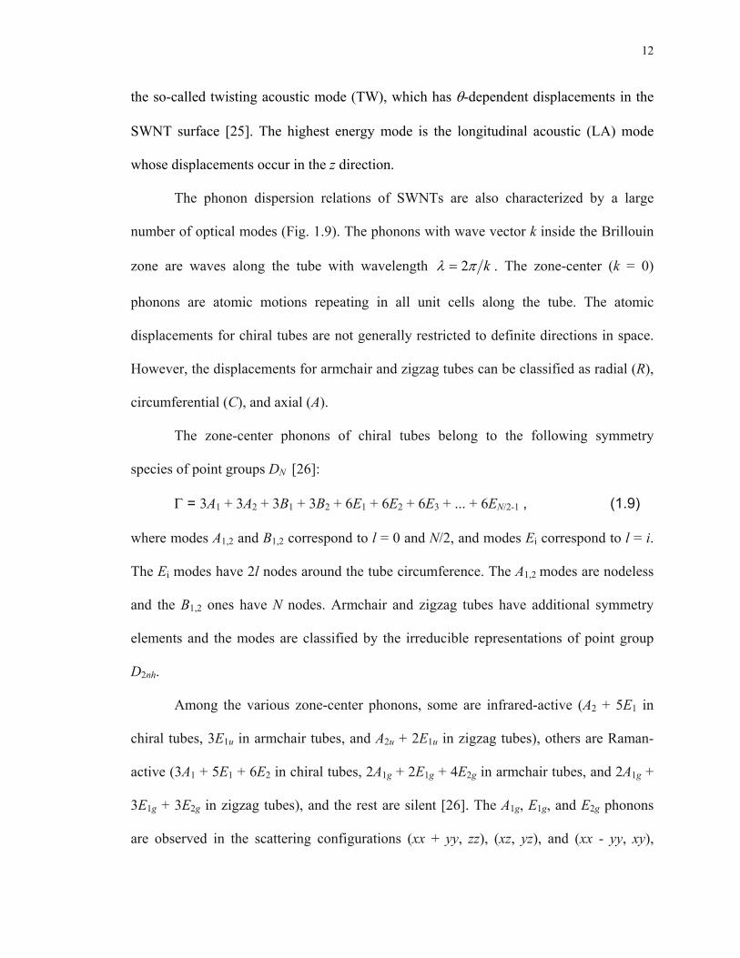
Figure 1.9………………………………………………………………………………...11
x
(a) Calculated phonon dispersion relations and (b) phonon density of states of a (10,10) metallic nanotube. The number of degrees of freedom is 120 and the number of distinct phonon branches is 66.
A typical Raman spectrum of SWNT ropes showing three characteristic features: radial breathing modes (RBM) originating from tubes with different diameters, the D-band, and the split G-band.
Figure 2.1………………………………………………………………………………...26
Cellular growth chart for the rat osteoblast MC3T3-E1 cells implanted on SWNT thin films. MTT colorimetric assay was applied to monitor primary osteoblastic cell viability. The cell culture reaches 100% confluency after about 5 days when the SWNT film is totally covered by the cells as fluorescent images show in the insert. The chart shows a regular behavior and normal growth rate of cells on SWNTs; data can be compared with viability of osteoblastic cells implanted on standard polystyrene for control. For the fluorescent images cells were stained using Calcein AM fluorescent dye (Invitrogen), 1 hour prior to rinsing with PBS. The cells were visualized under 10 X objective (Olympus) with 2.4 mm2 field of view, on the areas marked with crossing lines. The plot is in logarithmic scale and error bars represent the standard error of the mean of 4 different samples.
Figure 2.2………………………………………………………………………………...28
(a) Raman maps for the I(D)/I(G) intensity ratio of SWNT films before and after cell implantation. (b) Typical Raman spectra of pristine SWNT films (black and blue lines), and SWNTs after 8 days (yellow line) and after 31 days (red line) of exposure to cells/media system show a time-increasing trend for the D band.
Figure 2.3………………………………………………………………………………...30
(a) Sheet resistance of SWNTs exposed to cell-based system at variable time from cell implantation. Clear increase of sheet resistance in SWNT films is observed corresponding to increase in the exposure time to the cells. No significant increase in sheet resistance was observed for control samples (exposed to biological media only), but the increase due to the exposure to the cells was clearly observed for all samples after day 14. (b) Mean values of I(D)/I(G) intensities ratio averaged on 36 points for each map in Fig. 2.2 (maps for day 0, 8 and 31 are shown) plotted versus exposure time. I(D)/I(G) ratio increment is about 33% (within a 10-15% margin of error) after 31 days from cell implantation and the trend seems to become more evident as culture passes. A significant increase in I(D)/I(G) ratio is clear only after day 14 indicating that a higher degree of disorder (creation of defects, vacancies,
xi
formation of new covalent bonds via functionalization, etc.) has been introduced in the SWNT structure.
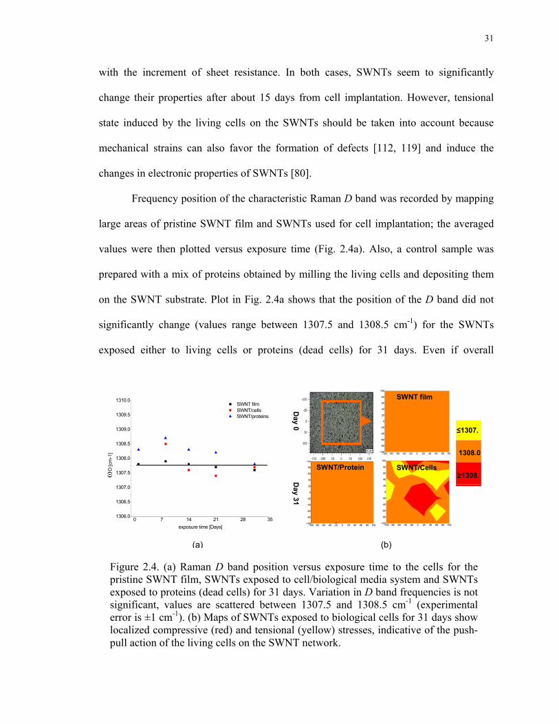
(a) Raman D band position versus exposure time to the cells for the pristine SWNT film, SWNTs exposed to cell/biological media system and SWNTs exposed to proteins (dead cells) for 31 days. Variation in D band frequencies is not significant, values are scattered between 1307.5 and 1308.5 cm-1 (experimental error is ±1 cm-1). (b) Maps of SWNTs exposed to biological cells for 31 days show localized compressive (red) and tensional (yellow) stresses, indicative of the push-pull action of the living cells on the SWNT network.
Figure 2.5………………………………………………………………………………...32
Raman signals (λexc.= 633 nm) in the range of RBM mode (150-350 cm-1) showing that both m-SWNT and s-SWNT are present in about the same ratio in the SWNT bundles after 31 days of cell exposure.
Figure 2.6………………………………………………………………………………...34
FTIR spectra of the SWNT film as deposited (black line), SWNT film exposed to biological media only (dark green line), SWNT film exposed to proteins (purple line) and SWNT film used for implantation of living cells (red line). All data were collected after 1 day of exposure to the cell/biological media systems. Sharp peaks in the range (2320-2360 cm-1) and (2850-2900 cm-1) arise from the background.
Figure 2.7………………………………………………………………………………...35
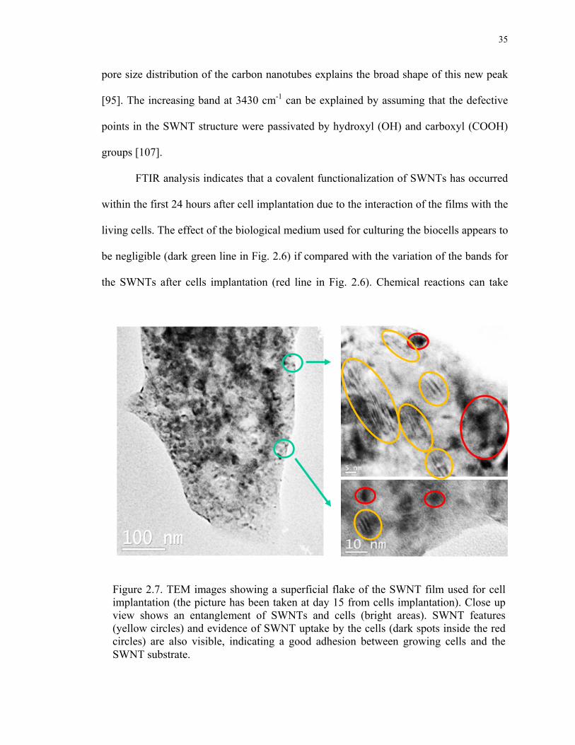
TEM images showing a superficial flake of the SWNT film used for cell implantation (the picture has been taken at day 15 from cells implantation). Close up view shows an entanglement of SWNTs and cells (bright areas). SWNT features (yellow circles) and evidence of SWNT uptake by the cells (dark spots inside the red circles) are also visible, indicating a good adhesion between growing cells and the SWNT substrate.
Figure 2.8………………………………………………………………………………...36
High resolution TEM images of (a) pristine SWNT bundles, (b) SWNTs exposed for 15 days to biological media only used as control and (c) SWNTs exposed for 15 days to cell/biological media system. SWNT bundles used for cell implantation clearly show severe wall damages; the “sharkskin” surface indicates a slow degradation of the SWNTs with the exposure time. Localized mechanical stress induced by the push-pull action of the living cells and superficial covalent functionalization of SWNTs due to bio-chemical
xii
interaction (cellular respiratory mechanism) are among the causes of such degradation.
Figure 3.1…………………………………………………………………………….......39
Atomic structure of B4C.
Figure 3.2………………………………………………………………………………...39
Boron-carbon phase diagram.
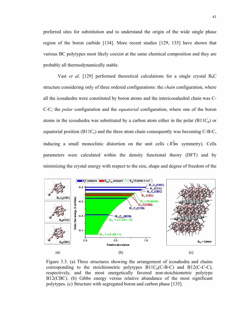
Figure 3.3………………………………………………………………………………...41
(a) Three structures showing the arrangement of icosahedra and chains corresponding to the stoichiometric polytypes B11Cp(C-B-C) and B12(C-C-C), respectively, and the most energetically favored non-stoichiometric polytype B12(CBC). (b) Gibbs energy versus relative abundance of the most significant polytypes. (c) Structure with segregated boron and carbon phase.
Figure 3.4………………………………………………………………………………...44
Raman spectra of single crystal B4C, (0001) surface, taken at excitation wavelengths of 515, 633, and 780 nm.
Figure 3.5………………………………………………………………………………...44
Interpretation of the Raman spectrum of B4C - (A) experimental spectrum, (B) theory for (a) B12(C-C-C), (b) polar B11Cp(C-B-C), and (c) equatorial B11Ce(C-B-C) configurations. Solid lines: Eg mode; dashed lines: A1g mode.
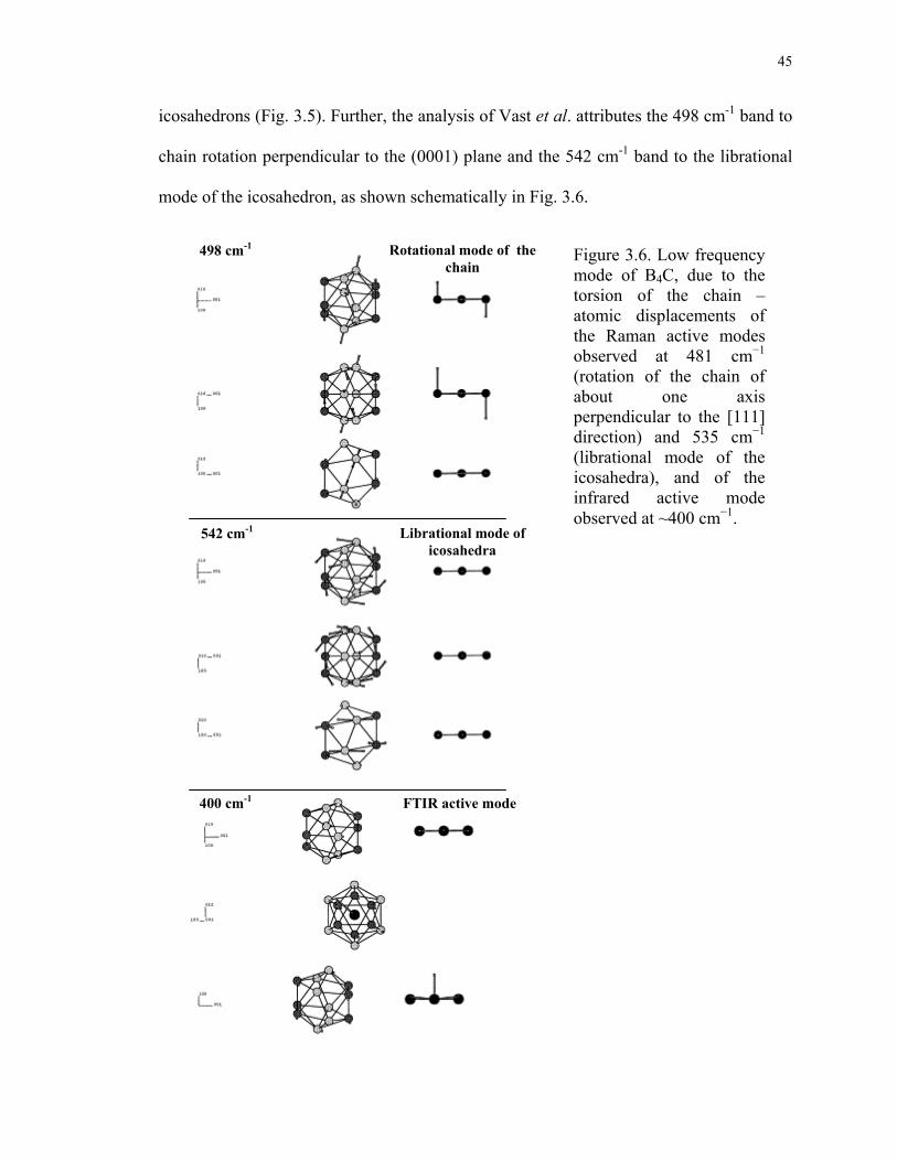
Figure 3.6………………………………………………………………………………...45
Low frequency mode of B4C, due to the torsion of the chain – atomic displacements of the Raman active modes observed at 481 cm−1 (rotation of the chain of about one axis perpendicular to the [111] direction) and 535 cm−1 (librational mode of the icosahedra), and of the infrared active mode observed at ~400 cm−1.
Figure 3.7………………………………………………………………………………...47
A typical Raman spectrum of amorphous/graphitic carbon showing characteristic D and G bands.
Figure 3.8………………………………………………………………………………...47
Carbon atoms motion in the (a) G and (b) D modes of vibration. Note that the G mode is due to the relative motion of sp2 carbon atoms and it can be found in the chain as well.
xiii
Figure 3.9………………………………………………………………………………...51
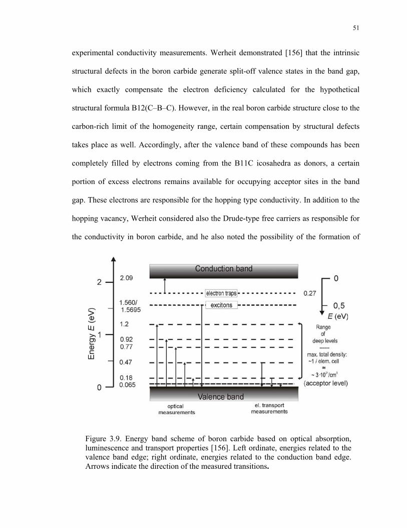
Energy band scheme of boron carbide based on optical absorption, luminescence and transport properties. Left ordinate, energies related to the valence band edge; right ordinate, energies related to the conduction band edge. Arrows indicate the direction of the measured transitions.
Figure 3.10……………………………………………………………………………….52
Absorption coefficient versus photon energy in B4.3C single crystal.
Figure 3.11……………………………………………………………………………….53
Photoluminescence spectrum of B4.3C single crystal at 290 K and 2.4 eV excitation energy. Squares, experimental results; thin solid line, averaged experimental results; bold solid line, recombination model of free excitons; bold dashed line, model for the transition of electrons between energy band and defect level.
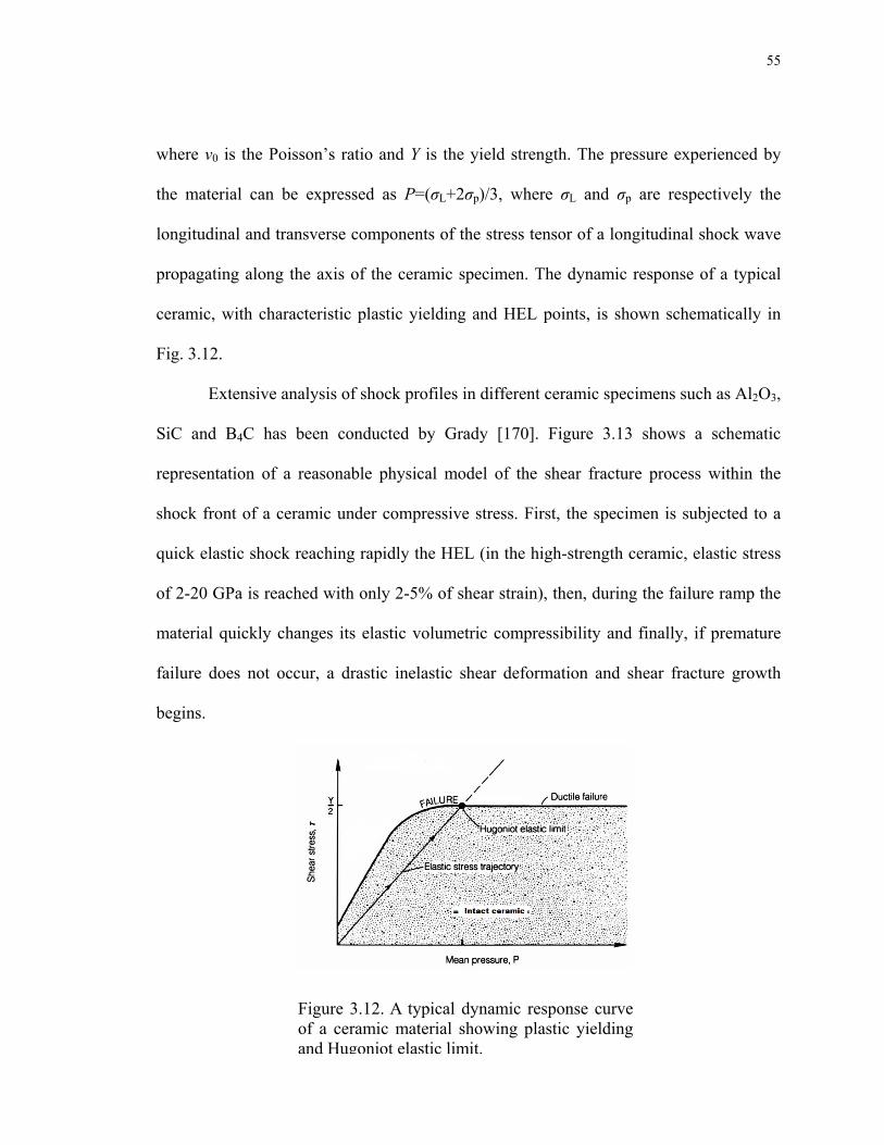
Figure 3.12……………………………………………………………………………….55
A typical dynamic response curve of a ceramic material showing plastic yielding and Hugoniot elastic limit.
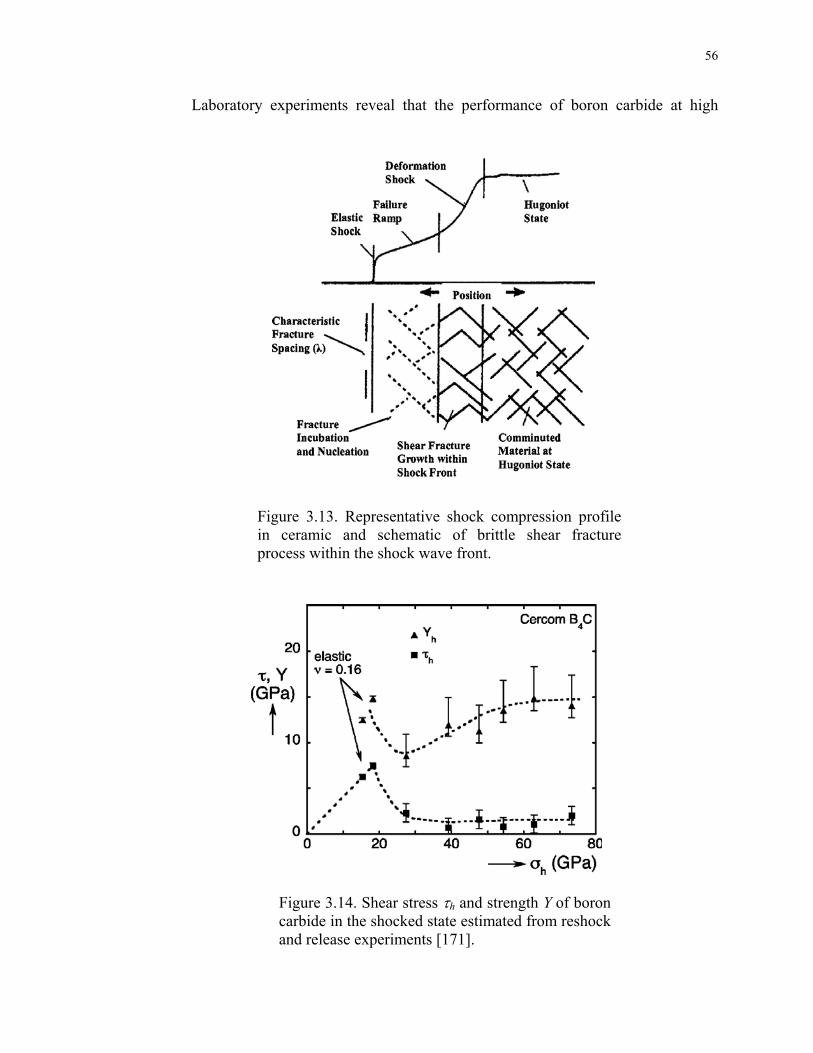
Figure 3.13……………………………………………………………………………….56
Representative shock compression profile in ceramic and schematic of brittle shear fracture process within the shock wave front.
Figure 3.14……………………………………………………………………………….56
Shear stress τh and strength Y of boron carbide in the shocked state estimated from reshock and release experiments.
Figure 3.15……………………………………………………………………………….57
Ballistic data on BC showing an abrupt drop in shear strength at impact pressures of 20-23 GPa.
Figure 3.16……………………………………………………………………………….58
A boron carbide ballistic target that comminuted during impact (left) and a HR TEM image n of a fragment produced by a ballistic test at impact pressure of 23.3 GPa (right). The lattice images on either side of the band correspond to the [1-101] direction of crystalline BC, and the loss of lattice fringes in the band indicates localized amorphization.
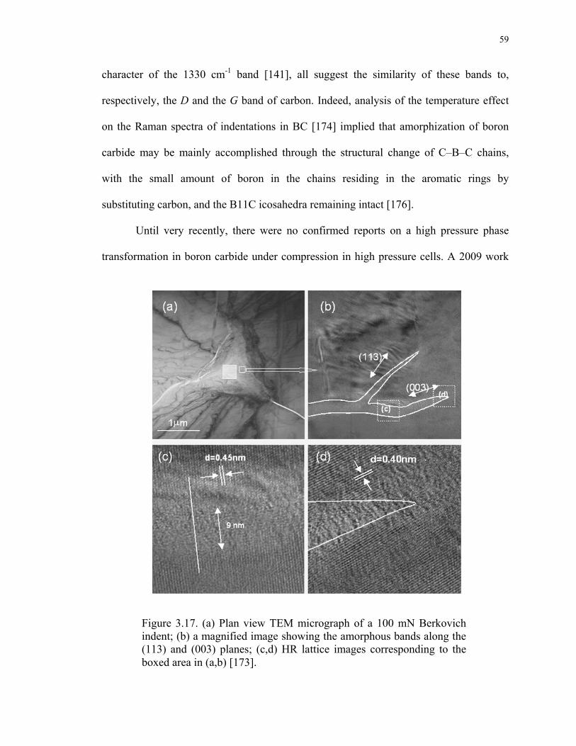
Figure 3.17………………………………………………………………………………59
xiv
(a) Plan view TEM micrograph of a 100 mN Berkovich indent; (b) a magnified image showing the amorphous bands along the (113) and (003) planes; (c,d) HR lattice images corresponding to the boxed area in (a,b).
Figure 3.18……………………………………………………………………………….60
Raman spectra of (a) pristine single crystal B4.3C; (b) indented single crystal; (c) indented hot-pressed polycrystalline sample; (d) scratch debris of a single crystal and (e) annealed scratch debris in air by using an argon ion laser with excitation wavelength of 514.5 nm.
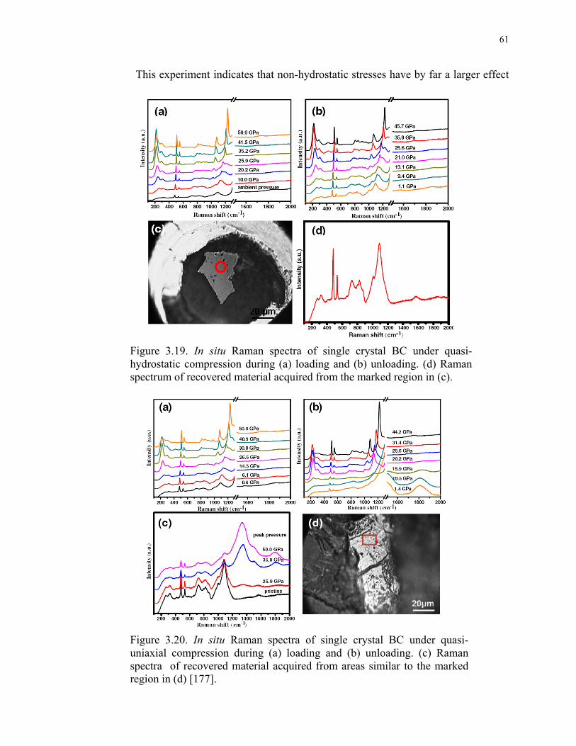
Figure 3.19……………………………………………………………………………….61
In situ Raman spectra of single crystal BC under quasi-hydrostatic compression during (a) loading and (b) unloading. (d) Raman spectrum of recovered material acquired from the marked region in (c).
Figure 3.20……………………………………………………………………………….61
In situ Raman spectra of single crystal BC under quasi-uniaxial compression during (a) loading and (b) unloading. (c) Raman spectra of recovered material acquired from areas similar to the marked region in (d).
Figure 3.21……………………………………………………………………………….62
First principles simulation of the stabilization of B11C(C-B-C) under hydrostatic and uniaxial compression. (a) Compressed volume vs. pressure. The square data represent the volume change with hydrostatic pressure, and the circle data correspond to the volume change with uniaxial stress along the C-B-C atomic chain. (b) Atomic configurations of the B4C unit cell at various pressures corresponding to data points in (a).
Figure 3.22……………………………………………………………………………….63
Diagrams of the steps proposed by Fanchini et al. required to transform B11Cp(C-B-C) into B12 and graphite at 10-4 GPa and 16 GPa. The transformation steps involve migration of C atom in the icosahedron from a polar to an equatorial site [B11Cp(C-B-C) to B11Ce(C-B-C)]; migration of the B atom in the chain from the central to a boundary site [B11Cp(C-B-C) to B11Ce(B-C-C)]; swapping of the equatorial icosahedral C atom with the boundary B atom in the chain [B11Ce(B-C-C) to B12(C-C-C)]; coalescence of the obtained (CCC) chains along the (113) planes, through a rotation of their axis around the [001] direction.
Figure 4.1………………………………………………………………………………...67
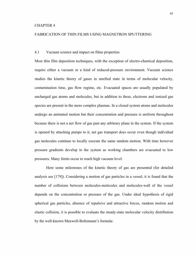
Density, mean free path, incidence rate, and monolayer formation versus pressure.
xv
Figure 4.2………………………………………………………………………………...69
Schematic of a film growth process.
Figure 4.3………………………………………………………………………………...69
Effect of temperature and gas pressure on film microstructure. Porous structure (voids and crystallites), densely packed grains, columnar grain and recrystallized grain structure are observed.
Figure 4.4………………………………………………………………………………...71
Schematic of energized plasma during sputtering (glow discharge). Upper insert shows a simplified model of film deposition.
Figure 4.5………………………………………………………………………………...77
Gibbs free energy of the B11Cp(C-B-C) and B12(C-C-C) polytypes as a function of silicon atoms concentration. It can be observed that the difference in Gibbs free energy between the stable polytype, B11C(1-y,p)Si(y,p)(C-B-C) and the most energetically favored minority polytype, B12(C-SiyC(1-y)-C) increase with the silicon content. Hence, silicon-containing boron carbide is less affected by disorder than the undoped one.
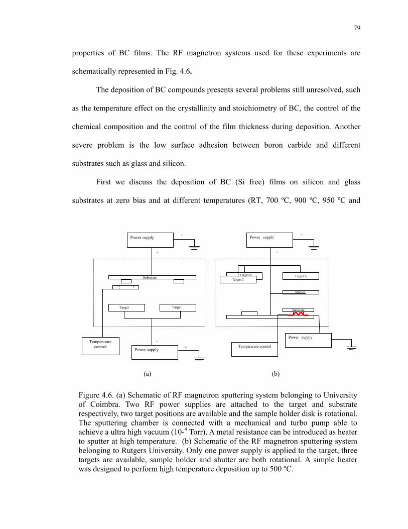
Figure 4.6………………………………………………………………………………...79
(a) Schematic of RF magnetron sputtering system belonging to University of Coimbra. Two RF power supplies are attached to the target and substrate respectively, two target positions are available and the sample holder disk is rotational. The sputtering chamber is connected with a mechanical and turbo pump able to achieve a ultra high vacuum (10-4 Torr). A metal resistance can be introduced as heater to sputter at high temperature. (b) Schematic of the RF magnetron sputtering system belonging to Rutgers University. Only one power supply is applied to the target, three targets are available, sample holder and shutter are both rotational. A simple heater was designed to perform high temperature deposition up to 500 ºC.
Figure 4.7………………………………………………………………………………...80
Set of sputtering deposition experiments performed at University of Coimbra. BC thin films were obtained by varying substrate bias from -30 to -170 V negative bias. Other experiments were carried out at zero bias but they were annealed at high temperature (up to 1000 ºC) after deposition. Many films flaked off because of the week adhesion between film and substrate.
Figure 4.8………………………………………………………………………………...81
xvi
(a) Optical microscopy images of flaked BC film deposited at zero bias and 700 ºC. (b) Raman spectra showing broad features from 200 to 1200 cm-1, characteristic of a-BC. Data are in agreement with recent publications.
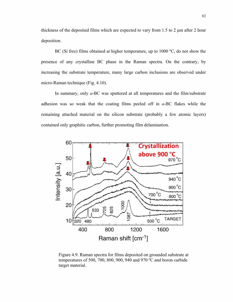
Figure 4.9…………………………………………………………………………...……82
Raman spectra for films deposited on grounded substrate at temperatures of 500, 700, 800, 900, 940 and 970 ºC and boron carbide target material.
Figure 4.10……………………………………………………………………………….83
(a) Optical images and (b) Raman spectra of films sputtered at different temperatures. Carbon D (1330 cm-1) and G (1580 cm-1) bands are observed. No crystalline BC was formed. No boron carbide features are observed but only Si peaks belonging to the substrate.
Figure 4.11……………………………………………………………………………….84
Infrared spectra showing the transmission bands for the α-BC flakes. The enhanced bands at ~1100 cm-1 are probably related to the icosahedra modes, while the bands at 600 and 1440 cm-1 could be associated with the presence of the carbon bonds.
Figure 4.12……………………………………………………………………………….85
SEM images of (a) unbiased sputtered a-BC, delaminating area leave discovered the Ti interlayer; (b) sputtered a-BC film deposited on Ti interlayer applying -170V substrate bias, the a-BC film has a strong adhesion with the silicon substrate and shows a nanogranular morphology.
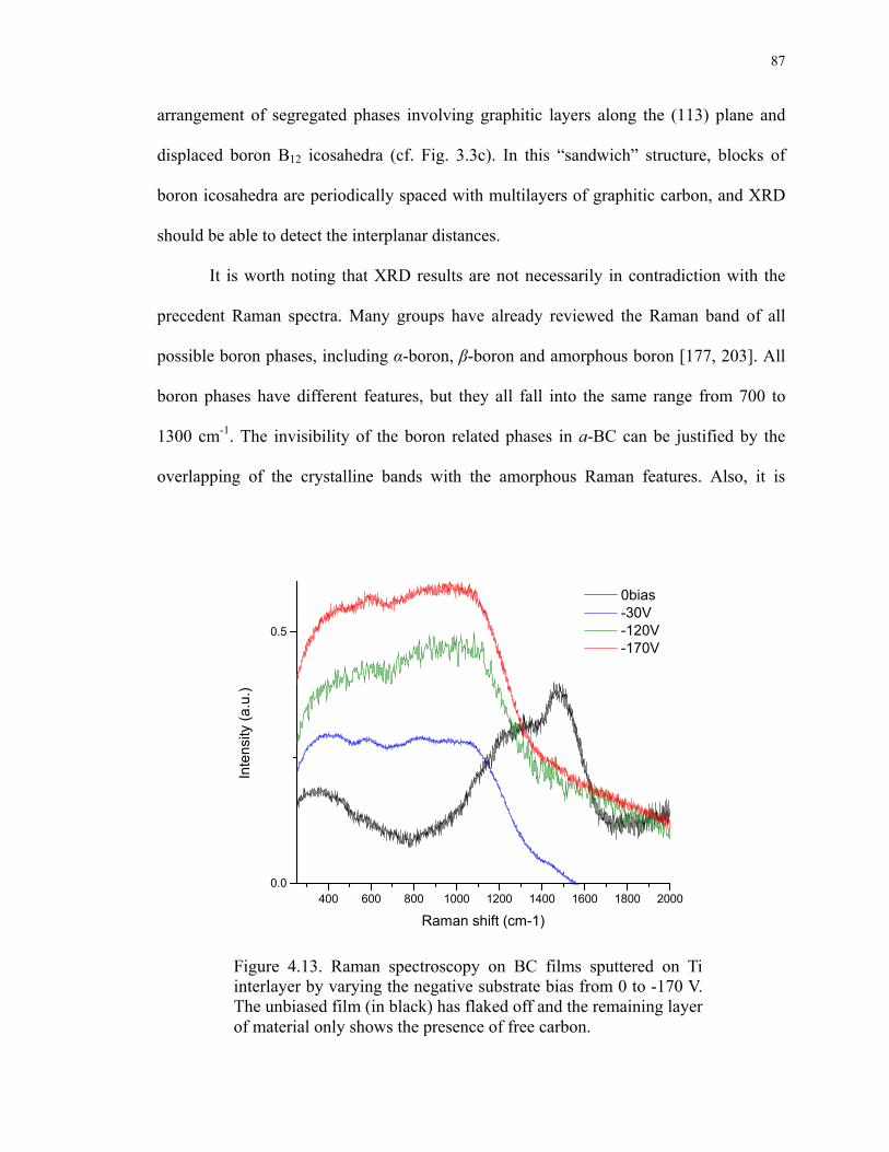
Figure 4.13……………………………………………………………………………….87
Raman spectroscopy on BC films sputtered on Ti interlayer by varying the negative substrate bias from 0 to -170 V. The unbiased film (in black) has flaked off and the remaining layer of material only shows the presence of free carbon.
Figure 4.14……………………………………………………………………………….88
XRD pattern of a BC film sputtered on top of Ti interlayer. The film was sputtered at RT, applying a negative bias of -70 V. The TiO2 peaks are shifted by about 1-2 degrees demonstrating that the interlayer is experiencing residual tensile stress after deposition. The small peaks are related to the presence of boron, probably β-B, and graphitic carbon.
Figure 4.15……………………………………………………………………………….90
xvii
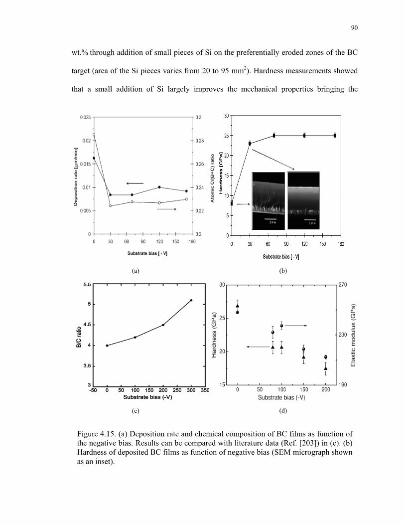
(a) Deposition rate and chemical composition of BC films as function of the negative bias. Results can be compared with literature data (Ref. [203]) in (c). (b) Hardness of deposited BC films as function of negative bias (SEM micrograph shown as an inset).
Figure 4.16……………………………………………………………………………….91
(a) Hardness and atomic C/(C+B) ratio of the as deposited BC:Si films as a function of the silicon content. (b) Evolution of the hardness of BC:Si coatings as a function of annealing temperature in protective atmosphere.
Figure 4.17……………………………………………………………………………….92
RF magnetron sputtering system belonging to Rutgers University: (a) external view, (b) open vacuum chamber, (c) close up view of target-substrate configuration, (d) designed heater.
Figure 4.18……………………………………………………………………………….93
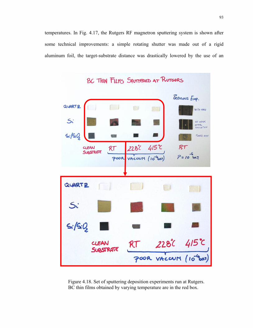
Set of sputtering deposition experiments run at Rutgers. BC thin films obtained by varying temperature are in the red box.
Figure 4.19……………………………………………………………………………….95
Raman spectroscopy on films sputtered at (a) RT and 230 ºC and (b) 415 ºC. Films were deposited by using the sputtering system implemented in Fig. 4.17. Formation of boric acid and boron oxide has been detected due to poor vacuum conditions during deposition.
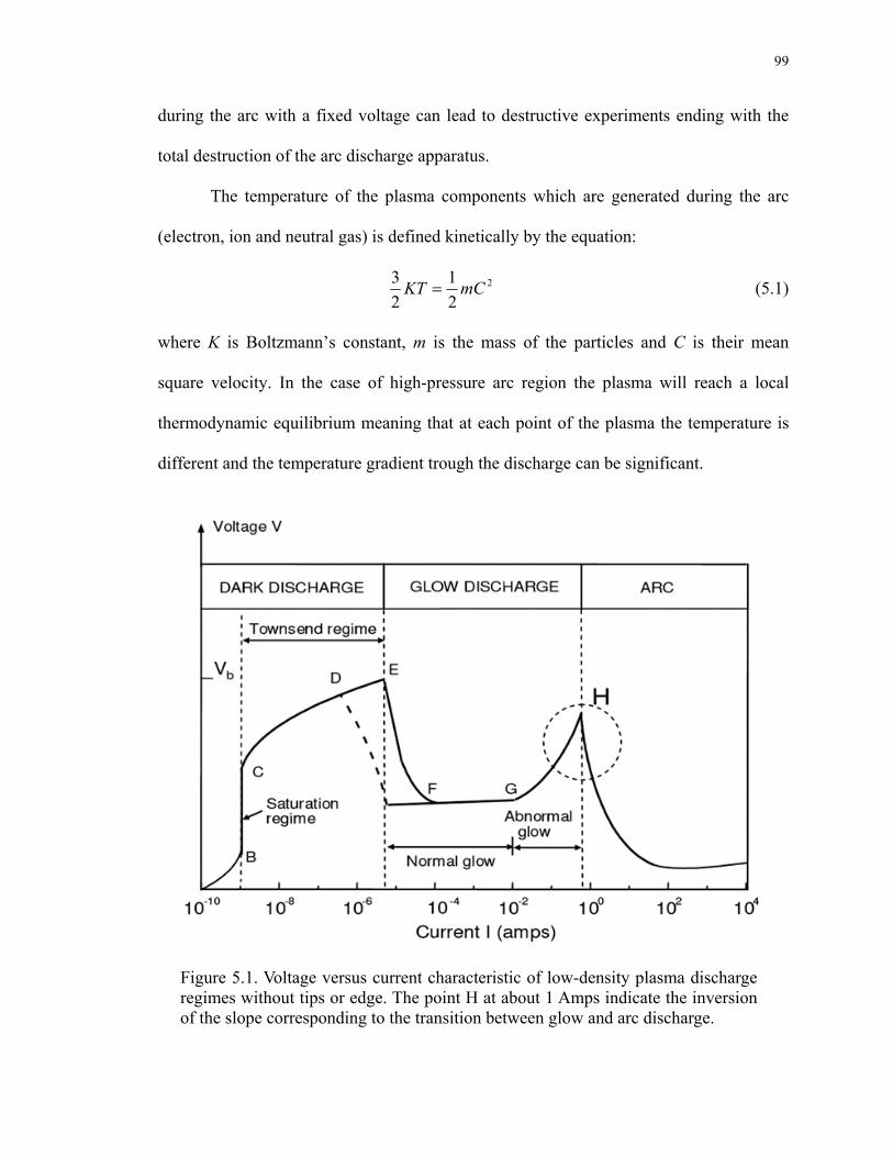
Figure 5.1………………………………………………………………………………...99
Voltage versus current characteristic of low-density plasma discharge regimes without tips or edge. The point H at about 1 Amps indicate the inversion of the slope corresponding to the transition between glow and arc discharge.
Figure 5.2……………………………………………………………………………….102
Linear fall in potential through the arc when ionization is produced in the gas between the two electrodes.
Figure 5.3……………………………………………………………………………….102
Illustration of arc discharge between two carbon electrodes. The positive anode presents a concave bright part called crater (c); the negative cathode is usually pointed and is left in darkness.
Figure 5.4……………………………………………………………………………….104
xviii
(a) Conventional circuit for dc electrical discharges in tubes. (b) Stabilization of the electric arc due to the ballast resistor Rb (C is the stable operating point).
Figure 5.5……………………………………………………………………………….110
Instrumental set up for the submerged arc discharge experiment: (a) schematic, (b) a photo of an actual setup. The boron carbide electrodes are obtained from hot pressed BC pieces, the ends of the electrodes are sharpened in order to promote the formation of the arc between them. The electrodes are submerged in liquid nitrogen/de-ionized water or inert gas and DC current is applied to them while the distance between the BC sharp points is slowly lowered until the anode touches the cathode to initiate an electric arc.
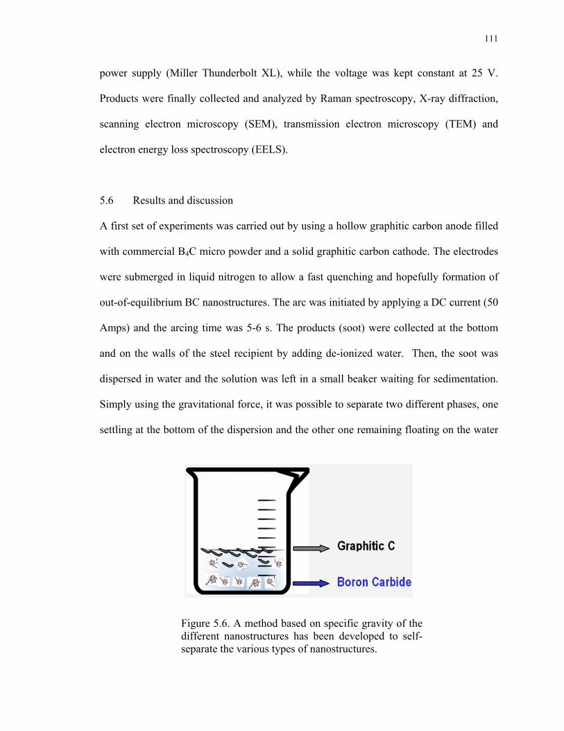
Figure 5.6……………………………………………………………………………….111
A method based on specific gravity of the different nanostructures has been developed to self-separate the various types of nanostructures.
Figure 5.7……………………………………………………………………………….112
Raman spectra of boron carbide soot obtained by submerged arc discharge between two graphitic electrodes. For the bottom part of the solution (black line), BC peaks already discussed in Chapter 4 are present. For the upper part of the solution (red line), larger amounts of carbon (D and G peaks) are detected. Peaks at ~520 cm-1 and 900 cm-1 come from Si substrate.
Figure 5.8……………………………………………………………………………….113
XRD spectra of boron carbide soot obtained by submerged arc discharge between two graphitic electrodes. BC peaks (squares) and C peaks (circles) indicate the presence of crystalline BC deposited on the bottom of the recipient and mostly graphitic carbon in the upper part of the beaker.
Figure 5.9……………………………………………………………………………….114
SEM images of collected soot performed obtained at an accelerating voltage of 10 kV and a working distance of 6 mm. Different nanostructures were formed during the arc discharge in liquid nitrogen: (a) nanograins, (b,c) nanotubes, (d) nanoribbons, and (e) rigid nanorods. The image in the center shows a low magnification image.
Figure 5.10……………………………………………………………………………...115
TEM and EELS analysis of soot particles: (a) low and (b) high resolution images of nanotubes; (c) a close-up view on the granular structure.
Figure 5.11……………………………………………………………………………...116
xix
Raman spectra of boron carbide soot obtained by arc discharge between two B4C electrodes submerged in DI water (red and green lines) and Ar gas (blue line). The spectrum of a B4C electrode is also shown for reference (black line). Inset shows an optical image of the soot for a DI water submerged experiment.
1
CHAPTER 1.
STRUCTURE AND PROPERTIES OF SINGLE-WALLED CARBON NANOTUBES
(SWNTs)
1.1 Atomic bonding and structure of SWNTs
Due to their particular electronic structure, carbon atoms allow various types of bonding
that are responsible for formation of structures with different properties. Each carbon
atom has six electrons, two of which fill the 1s orbital and do not contribute to bonding,
while the remaining four electrons fill the 2s and 2p orbitals and can form the sp3, sp2, or
sp hybridized bonds [1], as illustrated in Figure 1.1.
In diamond [1], the four valence electrons of each carbon atom occupy the sp3
hybridized orbital and create four equivalent σ covalent bonds to connect four other
carbon atoms in tetrahedral directions (Figure 1.2a). In graphite, three outer-shell
electrons of each carbon atom occupy the planar sp2 hybridized orbital to form three in-
plane σ bonds with an out-of-plane π bond. This makes strongly bonded planar
hexagonal networks of carbon atoms (graphite sheets) that are held together parallel to
each other by weak van der Waals forces (Figure 1.2b).
A single walled carbon nanotube (SWNT) can be viewed as a hollow cylinder
formed by rolling graphite sheets [2, 3] (Figure 1.2c). Bonding in SWNTs is essentially
sp2. However, the circular curvature of the sheet leads to quantum confinement and σ –
π rehybridization in which three σ bonds are slightly out of plane; for compensation, the
π orbital is more delocalized outside the tube. This bonding allows topological defects
such as pentagons and heptagons to be incorporated into the hexagonal network to form
2
capped, bent, toroidal, and helical nanotubes whereas electrons will be localized in
pentagons and heptagons because of redistribution of π electrons. The SWNT is called
defect free if it is of only hexagonal network and defective if it also contains topological
defects such as pentagons and heptagons, or other chemical and structural defects [4]. A
group of coaxial SWNTs is called a multi-walled carbon nanotube (MWNT) [5].
Figure 1.1. Bonding between carbon atoms: (a) sp3, (b) sp2, and (c) sp-hybridized orbitals.
Figure 1.2. Arrangement of carbon atoms in (a) diamond, (b) graphite, and (c) nanotube structure.
(a) (b) (c)
(a) (b) (c)
3
The SWNT can be uniquely characterized by a vector C in terms of a set of two
integers (n,m) corresponding to graphite vectors a1 and a2 (Fig. 1.3) [6]:
Figure 1.3. A nanotube (n,m) is formed by rolling a graphite sheet along the chiral vector C = na1 + ma2 on the graphite where a1 and a2 are graphite lattice vectors. The nanotube is also characterized by diameter |C| and the chiral angle θ with respect to the zigzag axis (θ = 0).
(a) (b) (c)
Figure 1.4. Typical nanotubes obtained by rolling a graphite sheet: (a) zigzag (n,0); (b) armchair (m,m); and (c) chiral (n,m), where n > m > 0 by definition.
4
21 aaC mn += (1.1)
The SWNT is constructed by rolling up the graphite sheet such that the two end-
points of the vector C are superimposed. This tube is denoted as (n,m) tube with diameter
given by
ππ
22 mnmnaD ++==
C (1.2)
where 21 aa ==a is lattice constant of graphite. The tubes with m = n are commonly
referred to as armchair tubes and m = 0 as zigzag tubes. Other tubes are generally called
chiral tubes with the chiral angle, θ, defined as that between the vector C and the zigzag
direction a1,
nm
m23tan 1
+= −θ (1.3)
Chiral angle θ ranges between 0º for zigzag (m = 0) and 30º for armchair (m = n) tubes.
For convention, a condition that mn ≥ is always applied. Examples of zigzag, armchair,
and chiral nanotubes are shown in Fig. 1.4.
The lattice constant and intertube spacing are required to generate a SWNT,
SWNT bundle, and MWNT. These two parameters vary with tube diameter or in radial
direction. The majority of experimental measurements and theoretical calculations
suggest the average C-C bond length of dcc = 0.142 nm (equivalent to
nm 0.24621 === aaa ) and the average intertube spacing of dtt = 0.34 nm [6].
Typically, experimentally observed SWNT diameter lays between 0.6 and 2.0 nm. Larger
SWNTs tend to collapse unless they are supported by other forces or surrounded by
neighboring tubes, as in MWNT. Typically, MWNT inside diameter is larger than 2 nm
5
and outside diameter is smaller than 100 nm. A SWNT rope is usually formed through a
self-organization process in which van der Waals forces hold individual SWNTs together
to form a triangular lattice with a constant (average intertube spacing) of 0.34 nm.
In addition to defect-free nanotubes, experimentally observed structures also
include the capped and bent [7], branched [8], and helical [9] MWNTs, and the capped
[10], bent [11], toroidal [12] SWNTs. In general, most SWNTs are defect-free whereas
MWNTs are relatively more defective, containing either topological defects (pentagons
and heptagons incorporated into the hexagonal network) or structural defects
(discontinuous or cone-shaped walls or bamboo structure). Incorporation of defects will
greatly affect nanotube properties; for example, the measured values of electrical and
thermal conductivity and elastic modulus can vary as much as several orders of
magnitude from sample to sample [4].
1.2 Electronic and optical properties of SWNTs
Due to their extremely small size and the highly symmetric structure, carbon nanotubes
are characterized by quantum confinement effects leading to remarkable electronic,
optical, and magnetic properties. In the simplest model [13, 14], the band structure of a
nanotube derived from the dispersion relation of a graphite sheet with the wave vector k
= (kx, ky) is expressed as follows:
( ) ⎟⎠⎞
⎜⎝⎛+⎟
⎠⎞
⎜⎝⎛
⎟⎟⎠
⎞⎜⎜⎝
⎛+±= akakakkkE yyxyx 2
1cos421cos
23cos41, 2γ (1.4)
where γ = 2.5 – 3.2 eV is the nearest neighbor hopping parameter and a = 0.246 nm is
lattice constant [4].
6
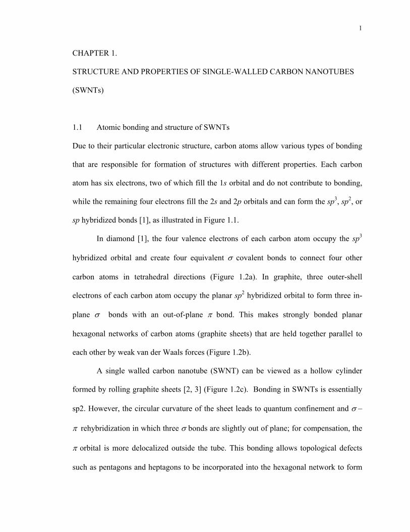
When the graphite sheet is rolled over to form a nanotube, a periodic boundary
condition is imposed along the tube circumference or the C direction. This condition
quantizes the two dimensional wave vector k along this direction. The k values satisfying
the relation qπ2=⋅Ck are allowed where q is an integer number. This leads to the
following condition at which metallic conductance occurs (i.e., band gap closes):
( ) qmn 3=− (1.5)
This suggests that one third of the tubes are metallic and two thirds are
semiconducting. A typical band structure of a metallic SWNT [15] is shown in Fig. 1.5.
The band gap of the semiconducting tube is given by
DdE cc
gγ2
= (1.6)
The above derivation does not consider the curvature effect or σ –
π rehybridization. This effect has been investigated using various approaches, including
Figure 1.5. Electronic band structure of a (10,10) metallic nanotube [15]. HO – highest occupied band; LU – lowest unoccupied band.
7
first principles calculations [16-19]. It is found that σ – π rehybridization can open up a
small band gap (~0.02 eV) for smaller (<1.5 nm) nonarmchair metallic tubes, but this
effect is rapidly disappearing with the tube diameter. In principle, only armchair tubes are
intrinsically metallic. However, for most discussions the metallization condition
( ) qmn 3=− and the band structure predicted from only the simplest π-orbital model
have been accepted.
The nanotube is a one-dimensional conductor and has to be aligned between two
electrodes for proper transport measurements. Due to σ – π rehybridization, the π
electron is more delocalized in a defect-free nanotube compared to graphite and therefore
SWNTs should be characterized by lower electrical resistivity values. However, because
SWNT ropes and MWNTs are often randomly oriented in the nanotube sheets, the actual
measured resistivity values are much higher than those of graphite. Only when the
measurements are carried out for the purified SWNT ropes or MWNTs aligned across
four electrodes, the electrical resistivity of carbon nanotube sheets is consistently
comparable with that of the highest quality graphite sheets (0.4 μΩ·m) [1, 20, 21].
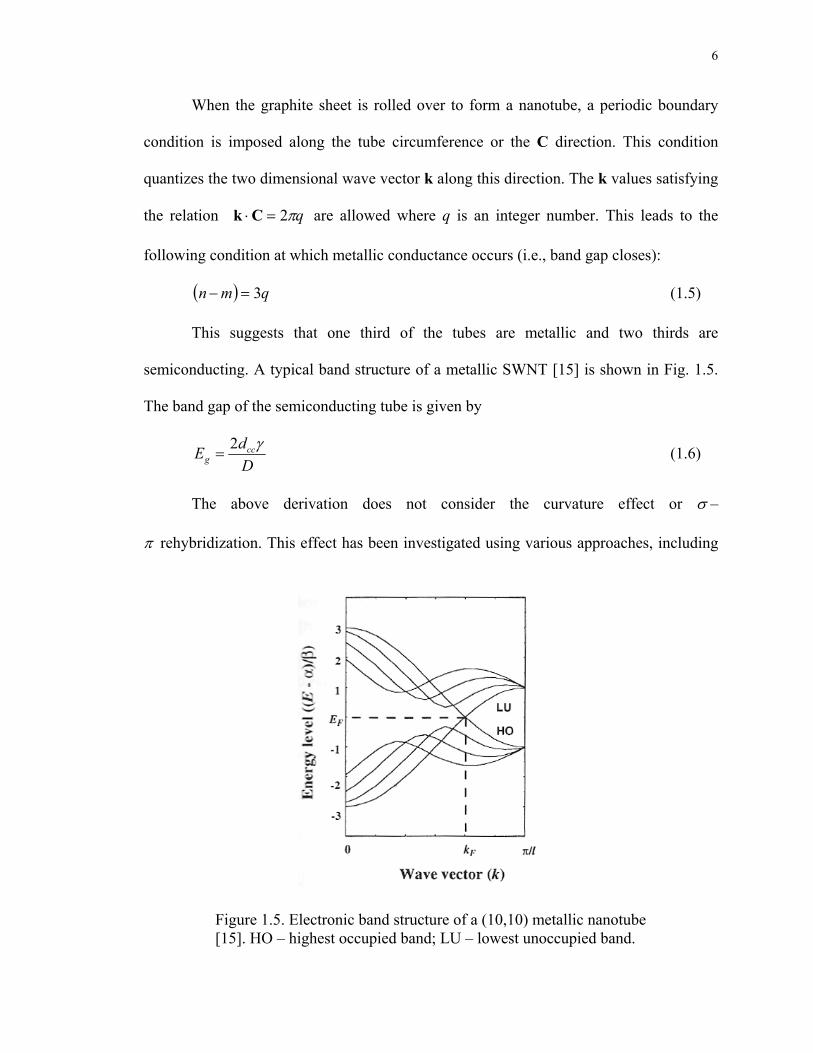
Defect-free SWNTs offer direct band gap and well defined band and subband
structure, which is ideal for optical and optoelectronic applications. A typical optical
spectrum measured for a SWNT rope is shown in Fig. 1.6 with that for a graphite sample
for comparison [22]. Three peaks for the SWNT ropes that cannot be observed in
graphite are attributed to symmetric transitions between the lowest subbands in
semiconducting (A and B) and metallic (C) tubes. The measured peak positions and
intensity can be correlated with electronic structures or tube chirality (n,m).
8
Optical and optoelectronic properties of SWNTs can be understood from their
Figure 1.6. (a) Optical spectra of colloidal graphite and an SWNT rope (offset for clarity). (b) Electronic density of states for semiconducting (A, B) and metallic (C) nanotubes showing how A, B, and C features can be attributed to symmetric electronic transitions between the lowest subbands [22].
Figure 1.7. Calculated electronic DOS of (10,10) and (11,8) metallic and (12,7) semiconducting nanotubes [4].
9
electronic band structure or density of states (DOS). The one-dimensional DOS of a
SWNT can be derived from that for graphite with the expression [4]
( )∑∞
−∞=
=m
mgal
εεγ
ερ ,324)( , (1.7)
where
( ) m
m
mg εεεε
εεε >
−= for ,
22;
( ) mmg εεεε <= for 0, ;
and
D
amnqm 3
3 γε
+−= .
Calculated electronic DOS of metallic (10,10), (11,8) and semiconducting (12,7)
nanotubes is shown in Fig. 1.7. The Fermi level is positioned to zero. The left- and right-
hand sides to the Fermi level define valence and conductance band, respectively. The
peak in DOS is called van Hove singularity. The optical transition occurs when electrons
or holes are excited from one energy level to another, denoted by Epq. The selection rules,
p = q, for interband transitions that are symmetric with respect to the Fermi level require
polarized light parallel to the tube axis, as shown by A, B, and C absorption features in
Fig. 1.6. The energy corresponding to the symmetric transition p = q for semiconducting
(S) and metallic (M) tubes follows the relations with one p-orbital approximation:
D
pdED
pdE ccMpp
ccSpp
γγ 6 and 2,, == . (1.8)
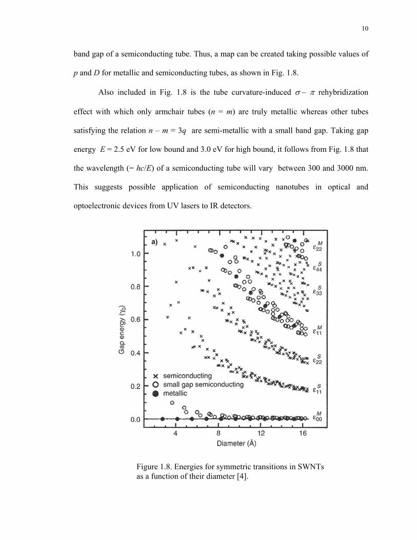
The number p (p = 1, 2, …) is used to denote the order of the valence and
conduction bands symmetrically located with respect to the Fermi level; p = 1 defines the
10
band gap of a semiconducting tube. Thus, a map can be created taking possible values of
p and D for metallic and semiconducting tubes, as shown in Fig. 1.8.
Also included in Fig. 1.8 is the tube curvature-induced σ – π rehybridization
effect with which only armchair tubes (n = m) are truly metallic whereas other tubes
satisfying the relation n – m = 3q are semi-metallic with a small band gap. Taking gap
energy E = 2.5 eV for low bound and 3.0 eV for high bound, it follows from Fig. 1.8 that
the wavelength (= hc/E) of a semiconducting tube will vary between 300 and 3000 nm.
This suggests possible application of semiconducting nanotubes in optical and
optoelectronic devices from UV lasers to IR detectors.
Figure 1.8. Energies for symmetric transitions in SWNTs as a function of their diameter [4].
11
1.3 Photon structure and vibrational properties of SWNTs
The phonon dispersion relations of SWNTs have been calculated using the tight binding
molecular dynamic simulation methods, adopted for the SWNT geometry by scaling
atomic force potential of a single graphite sheet [23, 24]. Fig. 1.9 shows the results
obtained for the phonon dispersion relations ω(k) and the phonon density of states
(PDOS) for two-dimensional graphite and a (10,10) nanotube. The PDOS for the (10,10)
nanotube is close to that for 2D graphite, reflecting the zone-folded SWNT phonon
dispersion.
As follows from Fig. 1.9, there are four acoustic modes in SWNTs. The lowest
acoustic modes are the transverse acoustic (TA) modes, which are doubly degenerate, and
have x and y displacements perpendicular to the SWNT z axis. The next acoustic mode is
Figure 1.9. (a) Calculated phonon dispersion relations and (b) phonon density of states of a (10,10) metallic nanotube [24]. The number of degrees of freedom is 120 and the number of distinct phonon branches is 66.
12
the so-called twisting acoustic mode (TW), which has θ-dependent displacements in the
SWNT surface [25]. The highest energy mode is the longitudinal acoustic (LA) mode
whose displacements occur in the z direction.
The phonon dispersion relations of SWNTs are also characterized by a large
number of optical modes (Fig. 1.9). The phonons with wave vector k inside the Brillouin
zone are waves along the tube with wavelength kπλ 2= . The zone-center (k = 0)
phonons are atomic motions repeating in all unit cells along the tube. The atomic
displacements for chiral tubes are not generally restricted to definite directions in space.
However, the displacements for armchair and zigzag tubes can be classified as radial (R),
circumferential (C), and axial (A).
The zone-center phonons of chiral tubes belong to the following symmetry
where modes A1,2 and B1,2 correspond to l = 0 and N/2, and modes Ei correspond to l = i.
The Ei modes have 2l nodes around the tube circumference. The A1,2 modes are nodeless
and the B1,2 ones have N nodes. Armchair and zigzag tubes have additional symmetry
elements and the modes are classified by the irreducible representations of point group
D2nh.
Among the various zone-center phonons, some are infrared-active (A2 + 5E1 in
chiral tubes, 3E1u in armchair tubes, and A2u + 2E1u in zigzag tubes), others are Raman-
active (3A1 + 5E1 + 6E2 in chiral tubes, 2A1g + 2E1g + 4E2g in armchair tubes, and 2A1g +
3E1g + 3E2g in zigzag tubes), and the rest are silent [26]. The A1g, E1g, and E2g phonons
are observed in the scattering configurations (xx + yy, zz), (xz, yz), and (xx - yy, xy),
13
respectively, for z axis along the tube (following Porto notation, Ref. [27]).
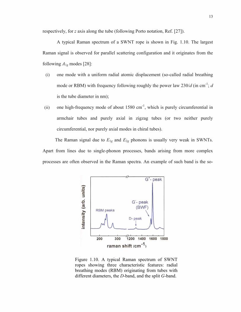
A typical Raman spectrum of a SWNT rope is shown in Fig. 1.10. The largest
Raman signal is observed for parallel scattering configuration and it originates from the
following A1g modes [28]:
(i) one mode with a uniform radial atomic displacement (so-called radial breathing
mode or RBM) with frequency following roughly the power law 230/d (in cm-1; d
is the tube diameter in nm);
(ii) one high-frequency mode of about 1580 cm-1, which is purely circumferential in
armchair tubes and purely axial in zigzag tubes (or two neither purely
circumferential, nor purely axial modes in chiral tubes).
The Raman signal due to E1g and E2g phonons is usually very weak in SWNTs.
Apart from lines due to single-phonon processes, bands arising from more complex
processes are often observed in the Raman spectra. An example of such band is the so-
Figure 1.10. A typical Raman spectrum of SWNT ropes showing three characteristic features: radial breathing modes (RBM) originating from tubes with different diameters, the D-band, and the split G-band.
14
called D (for disorder) band which is due to the presence of impurities and defects in
nanotubes (Fig. 1.10) and is characteristic for a wide range of carbon materials.
The Raman lines of the high-frequency A1g modes of the different tubes are closely
situated and modified by electron-phonon and electron-impurity interactions. The
modeling of the latter ones also faces the problem of considering far enough neighbors in
order to reproduce correctly the over-bending of the phonon branches of 2D graphite,
from which these modes originate. On the other hand, the lines of the RBM modes in the
measured spectra are often well-separated and can be used for structural characterization
of the SWNT samples (Fig. 1.10). It has to be also noted that the Raman spectra of
carbon nanotubes are usually measured under resonant conditions and nonresonant
spectra are rarely observed because of the low signal.
1.4 Mechanical properties of SWNTs
Because σ bonding is the strongest existing in nature, a nanotube that is structured with
all σ bonding is regarded as the ultimate fiber with the strength in its tube axis. Both
experimental measurements and theoretical calculations agree that a nanotube is as stiff
as or even stiffer than diamond with the highest Young’s modulus and tensile strength
[4]. The calculated mechanical properties of a (10,10) SWNT, an SWNT bundle, and
MWNTs are shown in Table 1.1 together with similar data for graphite and steel. It
should be noted that although the calculated data in Table 1.1 is in agreement with the
experiments on average [29-31], experimental results show broad discrepancy, in
particular for MWNTs, due to different amounts of defects present in MWNTs as
artifacts of different growth approaches.
15
Table 1.1. Mechanical properties of carbon nanotubes [32].
Young’s modulus
(GPa)
Tensile strength
(GPa)
Density
(g/cm3)
MWNT
SWNT
SWNT bundle
Diamond
Graphite (in-plane)
Steel
1200
1054
563
1220
350
208
~150
75
~150
90-225
2.5
0.4
2.6
1.3
1.3
3.5
2.6
7.8
In general, various types of defect-free nanotubes are stronger than graphite. This
is mainly because the axial component of σ bonding is greatly increased when a graphite
sheet is rolled over to form a seamless cylindrical structure or an SWNT. Young’s
modulus is independent on tube chirality, but it does depend on tube diameter. The
highest values for the Young’s modulus are obtained from tube diameters of 1 and 2 nm,
and are about 1 TPa. The mechanical properties of large tubes are approaching graphite,
while the smaller tubes are less stable mechanically. When SWNTs of different diameters
form a coaxial MWNT, the Young’s modulus of the MWNT takes the highest value of an
SWNT plus contributions from coaxial intertube coupling of van der Waals force.
Therefore, the Young’s modulus of MWNTs is higher than that of SWNTs, typically
reaching 1.1 to 1.3 TPa. On the other hand, when many SWNTs are held together in a
bundle or a rope, the weak van der Waals force induces a strong shearing among the
packed SWNTs, decreasing Young’s modulus of the bundle by as much as an order of
magnitude [4].
16
The elastic response of a nanotube is also very remarkable. Most hard materials
fail at strains of 1% or less due to the propagation of dislocations and defects. Both
theory and experiment show that SWNTs can sustain up to 15% tensile strain before
fracture [32]. Thus, the tensile strength of an individual nanotube can be as high as 150
GPa, assuming 1 TPa for Young’s modulus. Such a high strain is attributed to an elastic
buckling through which high stress is released. Elastic buckling also exists in twisting
and bending deformation of nanotubes. All elastic deformation including tensile
(stretching and compression), twisting, and bending in a nanotube is nonlinear, featured
by elastic buckling of up to ~15% or even higher strain. This is another unique property
of nanotubes, and such a high elastic strain for several deformation modes is originated
from σ – π rehybridization in SWNTs through which the high strain gets released.
1.5 Thermal properties of SWNTs
Because both graphite and diamond show extraordinary heat capacity and thermal
conductivity, it is expected that carbon nanotubes have similar thermal properties. Indeed,
experimental work confirms that at temperatures in excess of 100 K, specific heat of
SWNTs, SWNT bundles, and MWNTs is close to that of graphite, or about 700 mJ/gK.
However, due to quantum confinement effects at lower temperatures, heat capacity of
carbon nanotubes decreases drastically and reaches only 0.3 mJ/gK for a (10,10) SWNT,
~0 mJ/gK for a SWNT bundle, and 2-10 mJ/gK for MWNTs [33, 34].
The thermal conductivity of both SWNTs and MWNTs should reflect the on-tube
phonon structure, regardless of intertube coupling. Measurements of the thermal
conductivity of the bulk samples show graphite-like behavior for MWNTs, but quite
17
different behavior for SWNTs, specifically a linear temperature dependence at low T,
which is consistent with one-dimensional phonons. Both experimental and theoretical
work established that thermal conductivity of SWNT bundles and MWNTs at room
temperature varies from 1800 to 6000 W/mK, depending on the sample quality and tubes
alignment [34, 35].
1.6 Chemical properties and biocompatibility of SWNTs
Small radius, large specific surface and σ – π rehybridization make SWNTs very
attractive in chemical and biological applications because of their strong sensitivity to
chemical or environmental interactions. The chemical properties of interest include
opening, wetting, filling, adsorption, charge transfer, doping, intercalation, etc.
The nanotubes end is more reactive than the sidewall because of the presence of
pentagons or metallic catalysts occupying the opened ends and greater curvatures.
Opening nanotubes ends has been achieved by vapor phase oxidation, plasma etching,
and chemical reaction using acids such as HNO3. The opened end is typically terminated
with a functional group [36-38].
SWNTs are hydrophobic and do not show wetting behavior for most aqueous
solvents. It is reported that various organic solvents, HNO3, S, Cs, Rb, Se, and various
oxides such as Pb and Bi2O3 can wet nanotubes [39-41]. A nanotube provides capillary
pressure proportional to 1/D. Therefore, these wetting agents can be driven to fill inside
the nanotube by the capillary pressure. It should be also possible to fill non-wetting
agents inside a nanotube by applying an external pressure that is higher than the capillary
pressure.
18
Enhanced molecular adsorption and charge transfer can be expected for SWNTs.
Strong adsorption and charge transfer of oxygen to SWNTs have been experimentally
observed at room temperature. Theoretical calculations suggest that a number of gas
molecules, such as C8N2O2Cl2, O2, C6H12, C6H6, NO2, H2O, NH3, CH4, CO2, N2, H2, and
Ar can adsorb to various sites such as interstitial sites in the tube bundles, grooves above
the gap between two neighboring tubes, nanopores inside a tube, and surfaces of a single
tube [42-44]. In the charge transfer process, SWNTs can act as both donors and acceptors
depending on the nature of the adsorbed molecule. Molecular adsorption provides a
simple, noncovalent doping approach to turn SWNTs into p-type (with O2 or H2O
adsorption) or n-type (with C6H12) semiconductors. On the other hand, intercalation of
the alkali metals with nanotubes can be used to enhance metallic conductivity and
intercalation of halogens to enhance electrochemical capability of SWNTs for charge
transfer and storage [45-47].
The strong relationship between SWNTs electronic properties and their atomic
structure and mechanical deformations makes them very attractive for developing
extremely small sensors that are sensitive to the chemical, mechanical or physical
environment [48]. Nowadays, there is a strong need for smaller, faster, cheaper and
simpler biosensors able to extract more accurate and precise information from changes in
biological processes [49]. When the size of the material approaches the size of the
biomolecules (1-100nm), it directly interacts with the molecules. The reduction of the
size of sensing and transducing elements makes it possible to detect down to single
molecule. Sensing SWNT devices have already been fabricated for different applications
[50-52]. Many studies have also reported complex hybrid nanostructures, and
19
heterogeneous assembly of biological molecules with SWNTs was used as a template for
biomolecule assembly [53] or as conducting wires connecting biomolecules [54].
Carbon nanotubes may be considered a unique biomaterial. Owing to the
increasing interest in tissue engineering, SWNTs can be used as powerful tool for
monitoring and evaluating tissue growth [55]. There are mainly four areas that SWNTs
can be used in:
(i) Cell tracking and labeling [56]: the ability to track implanted cells in vivo and
non-invasively would help in evaluating the viability of the engineered tissue
and would also help in understanding of biodistribution and migration of
transplanted cells. SWNTs possess many properties desirable for optical
detection. For instance, SWNTs are characterized by optical transitions in the
near infrared (NIR) region between 900 nm and 1300 nm; this is an important
optical window because it minimizes interference problems such as tissue
absorbing, scattered light, autofluorescence and photobleaching [57]. SWNTs
display good photostability allowing long duration of tracking time. Moreover,
the SWNTs hydrophobic nature permits them to remain in the cells during
repeated cell divisions suggesting useful application for probing cell
proliferation and stem-cell differentiation. More sophisticated methods can be
introduced by modifying SWNTs with additional probes [58] or targeting
agents.
(ii) Sensing cellular behavior: the ability to monitor cellular physiology such as ion
transport, enzyme/cofactor interactions, protein and metabolite secretion and
cellular behavior such as matrix adhesion could help design better engineered
20
tissue. SWNTs could be used as contrast agent to monitor disease progress and
therapy responses by detecting the change in relevant physiological parameters
(i.e: pH, pO2 and glucose levels). SWNTs are ideal nanosensors because of their
large surface area that allows them to immobilize biological and chemical
compounds (i.e: DNA and proteins) and their nanosize which permits the
implantation of the probe without perturbing the system.
(iii) Augmenting cellular behavior: controlling the production or delivery of tissue-
inducing substances such as growth factor. SWNTs have already been used for
pharmaceutical delivery [59, 60] and they could be used for delivery of genetic
materials as well (i.e: DNA, RNA and bioactive proteins). The main advantage
of using SWNTs for this application is that they can be heterogeneously
functionalized.
(iv) Matrix enhancement: the ability to reinforce the structural support used for the
growth and development of engineered tissue. The commonly used biopolymers
(i.e., PLGA and PLA) lack the necessary mechanical strength, in addition they
are very difficult to functionalize. Mixing a small amount of SWNTs with the
polymer, significant improvement in the mechanical strength of the composite
scaffolds has been observed [61]. In vitro experiments demonstrated that SWNT
can support the grown of different cell types such as muscle [62], fibroblasts,
osteoblasts [63] and even neurons that can be grown on patterned arrays of
carbon nanotubes creating neural networks [64] .
Although SWNTs appears to be a good substrate for cellular growth and an
extremely powerful tool for biosensors, there is a debate in literature regarding the
21
cytotoxicity of SWNTs. Several in vitro studies reported necrosis and degeneration of
human cells exposed to SWNTs [65], formation of granulomas and pulmonary
inflammation [66]. On the other hand many experiments have shown that SWNT can
support the growth of different cells such as smooth muscle [67], fibroblasts [62]and
osteoblasts [63].
Any material of SWNT dimensions has the potential to be cytotoxic and even
carcinogenic if it does not degrade quickly. New approaches are being developed to
mitigate the potential cytotoxicity of SWNTs. For instance, it has been demonstrated that
functionalized SWNTs are inert [68], also it has been found that SWNTs can be
catalytically biodegraded by particular enzymes [69].
22
CHAPTER 2
DEGRADATION OF SINGLE-WALLED CARBON NANOTUBES STRUCTURE BY
LIVING OSTEOBLAST CELLS IN BIO-IMPLANTATION
2.1 Motivation and research outline
Single-walled carbon nanotubes (SWNTs) combine unique electronic and optical
properties with high mechanical strength and high thermal conductivity [70, 71]; for this
reason over the last decades, scientists have been exploring SWNT for a variety of
different applications [72-74]. Depending on their diameter and chirality, SWNTs are
either one-dimensional metals or one-dimensional semiconductors suitable for fabrication
of single electron transistors [75, 76] and field-effect transistors [77, 78]. Electronic
devices based on SWNTs are promising for many other applications, ranging from
molecular quantum wires [79] to electromechanical devices [80] and chemical/biological
sensors [56, 81-84]. Recently, SWNTs have also received high attention in biomedical
research as a potential substrate for cellular growth [55, 85-87]. However, the presumed
cytotoxicity of SWNTs obliges scientists to investigate more on the effective risk of
using SWNTs in living systems. Although some controversial studies and theories have
been lately suggested [69, 88-90], it is generally accepted that chemical functionalization
of the SWNT surface could mitigate the potential toxic effect associated with the
nanotubes [55]. Recently, a detailed study showed total biodegradation of SWNTs in
presence of human myeloperoxidase (hMPO), an enzyme known to be responsible for the
degradation of implantable polymeric materials [69]. In vitro analysis confirmed that
biodegraded SWNTs do not generate pulmonary inflammatory response that intact
23
SWNTs have shown to be responsible for. This finding reopens the debate about the use
of nanotubes in biomedical applications.
At present, basic information about interactions between SWNTs and
cells/biological media systems is missing. This study aims at establishing a correlation
between the variations in fundamental properties, such as the electrical conductivity, and
variations in structural characteristics of SWNT films exposed to specific conditions.
Raman spectroscopy and Fourier transform infra-red spectroscopy (FTIR) are shown to
be powerful tools for detailed analysis of the electronic changes of SWNT films engaged
in implantation of living cells.
2.2 Experimental approach
Interaction of cells/biological media system with carbon nanotubes is expected to affect
both their structure and their electronic properties via mechanical and/or chemical
modifications. It has been already extensively shown by previous studies [91, 92] that
after reaction of carbon nanotubes with host materials, dopants are intercalated either
inside or between the tubes in the case of SWNTs, or in the inter-shell space in the case
of multi-walled carbon nanotubes (MWNTs). Transformation of SWNTs due to
electrochemical doping has been reported in many papers [93-96] and it has been
explained for the first time by Chen et al. [95], who suggested a co-intercalation
mechanism of large solvent molecules into the SWNT bundles and a side reaction at the
electrode surface.
Changes in the electronic and phonon state of carbon nanotubes are easily
detectable by the use of Raman spectroscopy. The presence of van Hove singularities in
24
the one dimensional joint density of electronic states (JDOS) of carbon nanotubes leads
to a strong and unique electron-phonon coupling responsible for an unusual enhanced
resonance Raman effect. A detailed study on the nature of the typical vibration modes
observed for Raman scattering in SWNTs is discussed by Dresselhaus et al. [23, 97, 98].
The resonance Raman effect makes possible not only identification of vibrational and
rotational modes of SWNT at a single nanotube scale but also determination of their
structural properties such as diameter and chirality [99, 100] . It is not surprising, then,
that today Raman spectroscopy is the most powerful and widely used tool for
investigation of structural and electronic modifications of individual SWNTs [101].
Carbon materials are characterized by two strong first-order Raman features known as the
D band (at ~1250-1450 cm-1) and the G band (1500-1605 cm-1). In particular, the D band
is a dispersive band and its shape, peak width, intensity and position varies with the types
of carbon and the particle size [102]. In SWNTs, the D band is related to sp2 hybridized
carbon and represents the breathing mode of each graphitic ring. Also, the G band is
characteristic of the graphitic layers and in the Raman spectra of SWNTs it is a double
feature corresponding to the tangential and radial vibrations of the carbons along the
circumferential direction (G-) and along the direction of the nanotube axis (G+).
Variations of the Raman signal in the spectral range of the D band provide information
on the disorder state of the graphitic rings and the presence of induced defects in the
nanotube skeleton. The G band is instead associated with the tangential modes and a shift
of this band gives additional information about the C-C bond length and the Fermi energy
rises in the tube structure [91].
An additional characteristic feature in the Raman spectra of SWNTs is the radial
25
breathing mode (RBM) associated with the in-phase vibrations of the carbon atoms in the
radial direction. The RBM mode, which is strongly dependent on the diameter d and
chirality (n,m) of SWNTs, makes it possible to detect the occurrence of selective
reactions and/or transformations of metallic and semiconducting SWNTs by monitoring
the changes in their corresponding Raman intensities (in the spectral range of 150-350
cm-1) [81].
Further information on the vibrational state and the effect of cells on the SWNT
films can be obtained by Fourier transform infra-red (FTIR) spectroscopy. This technique
is particularly advantageous in identification of active chemical bonding and molecular
structure of SWNTs, but it has much poorer spatial resolution compared to Raman and it
is very sensitive to the amount of water and carbon dioxide present in the atmosphere.
Finally, scanning (SEM) and transmission (TEM) electron microscopy techniques were
employed to provide direct observation of the changes in SWNT as a result of
interactions with cells/biological media.
Osteoblast precursor mouse MC3T3-E1 cells and purified SWNT bundles were
used in this study. The SWNTs were purified and dispersed in water following the
protocol reported by Xu et al. and Eda et al. [103, 104]. The SWNT suspension (35 mL)
was deposited on 220 μm pore size filter mixed-cellulose ester membranes (MCE,
Millipore) forming free standing SWNT films. The SWNT thin films (200-300 nm in
thickness) were then placed on glass slides (Fisher Scientific) and successively cut into
uniform circular samples (d = 1.3-1.2 cm). The obtained SWNT samples were finally
dried in the oven and sterilized under UV light (254 nm) prior to living cells exposure.
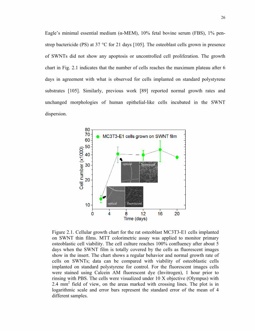
MC3T3-E1 osteoblastic cells plated at 5000 cells/well were supplemented with
strep bactericide (PS) at 37 °C for 21 days [105]. The osteoblast cells grown in presence
of SWNTs did not show any apoptosis or uncontrolled cell proliferation. The growth
chart in Fig. 2.1 indicates that the number of cells reaches the maximum plateau after 6
days in agreement with what is observed for cells implanted on standard polystyrene
substrates [105]. Similarly, previous work [89] reported normal growth rates and
unchanged morphologies of human epithelial-like cells incubated in the SWNT
dispersion.
Figure 2.1. Cellular growth chart for the rat osteoblast MC3T3-E1 cells implanted on SWNT thin films. MTT colorimetric assay was applied to monitor primary osteoblastic cell viability. The cell culture reaches 100% confluency after about 5 days when the SWNT film is totally covered by the cells as fluorescent images show in the insert. The chart shows a regular behavior and normal growth rate of cells on SWNTs; data can be compared with viability of osteoblastic cells implanted on standard polystyrene for control. For the fluorescent images cells were stained using Calcein AM fluorescent dye (Invitrogen), 1 hour prior to rinsing with PBS. The cells were visualized under 10 X objective (Olympus) with 2.4 mm2 field of view, on the areas marked with crossing lines. The plot is in logarithmic scale and error bars represent the standard error of the mean of 4 different samples.
fluorescent
fluorescent
optical
optical
27
In situ micro-Raman spectra were recorded at room temperature in a
backscattering geometry under excitation wavelength of 633 nm using a Renishaw InVia
Raman microspectrometer. Raman maps were collected by scanning with the laser a large
area (200 x 200 μm) of an SWNT film before and after cell implantation; the collected
spectra were then analyzed by Wire 2.0 software for peak fitting and mapping.
Transmittance spectra ranging from 900 to 4000 cm-1 were acquired at normal incidence
using a Perkin Elmer Lamda 20 FTIR spectrophotometer.
Electrical analysis of SWNTs exposed to cell-based system was carried out using
an Agilent VEE Pro instrument. Silver ohmic contacts were attached to the SWNT films
and the four-probe resistivity measurements were recorded by Van der Pauw method
[106] applying a voltage sweep ramp.
TEM images were obtained using a Topcon 002B transmission electron
microscope operating at 200 kV. Samples were prepared by dissolving the SWNT films
in aqueous solutions at 1 wt.% of sodium dodecyl sulfate (SDS); the SWNT suspension
was further subjected to gentle sonication for about 15 minutes and finally deposited by
drop casting on holey carbon grids.
2.3 Results and discussion
Raman maps for the I(D)/I(G) intensity ratio of SWNT films before and after cell
implantation are shown in Fig. 2.2. The increasing intensity of the D peak with the
exposure time of the SWNT films to the cells/media system suggests that a higher degree
of structural disorder is present in the graphitic rings composing SWNTs. During the
interaction between SWNTs and the cells/biological media system, it appears possible
28
that the SWNTs could have been damaged by the introduction of defects where carbon
rings were broken, carbon atoms were missing and localized C=C bonds were created
either by chemical processing or by mechanical stress induced by the push-pull action of
the living cells. Furthermore, oxygen-containing groups might have been added to
Figure 2.2. (a) Raman maps for the I(D)/I(G) intensity ratio of SWNT films before and after cell implantation. (b) Typical Raman spectra of pristine SWNT films (black and blue lines), and SWNTs after 8 days (yellow line) and after 31 days (red line) of exposure to cells/media system show a time-increasing trend for the D band.
I(D)/I(G)
(a)
SWN
T/Cells
SWN
T films
<0.5
0.55
0.6
0.7
>0.75
0.65
Day 0 Day 8 Day 31
(b)
-100 -80 -60 -40 -20 0 20 40 60 80 100-100
-80
-60
-40
-20
0
20
40
60
80
100
-100 -80 -60 -40 -20 0 20 40 60 80 100-100
-80
-60
-40
-20
0
20
40
60
80
100
-100 -80 -60 -40 -20 0 20 40 60 80 100-100
-80
-60
-40
-20
0
20
40
60
80
100
-100 -80 -60 -40 -20 0 20 40 60 80 100-100
-80
-60
-40
-20
0
20
40
60
80
100
-100 -80 -60 -40 -20 0 20 40 60 80 100-100
-80
-60
-40
-20
0
20
40
60
80
100
1200 1350 1500 16500.00
0.05
0.10
0.15
0.20
0.25 SWNT film Day 0 SWNT film Day 31 SWNTs/Cells Day 8 SWNTs/Cells Day 31
I(D)/I
(G)
[a.u
.]
Raman Shift [cm-1]
29
stabilize the wall defective structure leading to functionalization of the SWNTs with the
formation of hydroxyl (OH) and carboxyl groups (COOH), in accordance with literature
data [107]. The fact that the D peak is increasing in intensity but not changing its
Lorenzian line shape suggests that structural disorder is introduced in the SWNT bundles
without evident formation of amorphous carbon [108]. The intensity of the second-order
overtone G* band at ~2600 cm-1, which is not disorder-induced, does not vary with
exposure time (data not shown), confirming that amorphous carbon is not responsible for
the increasing intensity of the D band.
It is well known that introduction of defects, such as vacancies, disorder, chemical
modifications and bending in the SWNTs can lead to significant change in the electronic
properties [109-113] due to the local destruction of the electron-hole symmetry of the π-
π* states, and to the formation of new structures in the densities of states such as tight-
binding of the carbon π bands or quantum confinements (intratube quantum dots) etc.
[114-118]. Similarly, in situ electrical measurements have revealed that the conductance
of mechanically strained carbon nanotubes can significantly drop and theoretical
simulations indicate that this effect is owing to the formation of local sp3 bonds created
during the mechanical deformation [80].
Conductivity measurements in Fig. 2.3 reveal a time-dependent increase in sheet
resistance of the SWNT bundles exposed to cell implantation. Conversely, SWNT films
exposed to biological media only did not significantly modify their resistance. The
increasing rate of the sheet resistance with the exposure time of SWNTs to cells strongly
suggests a “dynamic” interaction between living cells and SWNTs rather than merely
mechanical attachment of the cells to the films. If the resistance increase were primarily
30
due to the simple attachment of the cells, it should have saturated after about 5 days,
when the cell number reaches its maximum (cf. growth chart in Fig. 2.1) and the cells
uniformly cover the SWNT substrate. In fact, an even steeper increase in resistance is
observed at day 15 after the cell number saturation confirming a “dynamic” SWNTs-cells
interaction.
By comparing the Raman analysis with the electrical results it is evident that the
increasing trend of the intensities ratio I(D)/I(G) with the exposure time correlates well
Figure 2.3. (a) Sheet resistance of SWNTs exposed to cell-based system at variable time from cell implantation. Clear increase of sheet resistance in SWNT films is observed corresponding to increase in the exposure time to the cells. No significant increase in sheet resistance was observed for control samples (exposed to biological media only), but the increase due to the exposure to the cells was clearly observed for all samples after day 14. (b) Mean values of I(D)/I(G) intensities ratio averaged on 36 points for each map in Fig. 2.2 (maps for day 0, 8 and 31 are shown) plotted versus exposure time. I(D)/I(G) ratio increment is about 33% (within a 10-15% margin of error) after 31 days from cell implantation and the trend seems to become more evident as culture passes. A significant increase in I(D)/I(G) ratio is clear only after day 14 indicating that a higher degree of disorder (creation of defects, vacancies, formation of new covalent bonds via functionalization, etc.) has been introduced in the SWNT structure.
0 7 14 21 28 35
1.0
1.5
2.0
2.5
3.0
3.5 SWNT films SWNT/cells SWNT/media
She
et R
esis
tanc
e [K
Ω/s
q]
exposure time [Days]0 7 14 21 28 35
0.50
0.55
0.60
0.65
0.70
0.75 SWNT films SWNT/cells SWNT/media
I(D)/I
(G)
[a.u
.]
exposure time [Days](a) (b)
31
with the increment of sheet resistance. In both cases, SWNTs seem to significantly
change their properties after about 15 days from cell implantation. However, tensional
state induced by the living cells on the SWNTs should be taken into account because
mechanical strains can also favor the formation of defects [112, 119] and induce the
changes in electronic properties of SWNTs [80].
Frequency position of the characteristic Raman D band was recorded by mapping
large areas of pristine SWNT film and SWNTs used for cell implantation; the averaged
values were then plotted versus exposure time (Fig. 2.4a). Also, a control sample was
prepared with a mix of proteins obtained by milling the living cells and depositing them
on the SWNT substrate. Plot in Fig. 2.4a shows that the position of the D band did not
significantly change (values range between 1307.5 and 1308.5 cm-1) for the SWNTs
exposed either to living cells or proteins (dead cells) for 31 days. Even if overall
(a) (b)
Figure 2.4. (a) Raman D band position versus exposure time to the cells for the pristine SWNT film, SWNTs exposed to cell/biological media system and SWNTs exposed to proteins (dead cells) for 31 days. Variation in D band frequencies is not significant, values are scattered between 1307.5 and 1308.5 cm-1 (experimental error is ±1 cm-1). (b) Maps of SWNTs exposed to biological cells for 31 days show localized compressive (red) and tensional (yellow) stresses, indicative of the push-pull action of the living cells on the SWNT network.
Day 0
Day 31
-100 -80 -60 -40 -20 0 20 40 60 80 100-100
-80
-60
-40
-20
0
20
40
60
80
100
-100 -80 -60 -40 -20 0 20 40 60 80 100-100
-80
-60
-40
-20
0
20
40
60
80
100
≤1307.5
1308.0
≥1308.SWNT/Cells SWNT/Protein
-100 -80 -60 -40 -20 0 20 40 60 80 100-100
-80
-60
-40
-20
0
20
40
60
80
100
SWNT film
0 7 14 21 28 351306.0
1306.5
1307.0
1307.5
1308.0
1308.5
1309.0
1309.5
1310.0 SWNT film SWNT/cells SWNT/proteins
ωD
[cm
-1]
exposure time [Days]
32
variations in vibrational frequencies were not observed, local tensional states for SWNTs
exposed to living cells were detected by visualization of Raman mapping data (Fig. 2.4b).
No change in D band position was observed for the SWNTs exposed to the proteins
indicating that the SWNT network experiences weak tensional and compressive states
due to the dynamic action of the cells (a push-pull mechanism owing to breathing,
moving and growing of the cells). In any case, the physical interaction between SWNTs
and cells does not affect the overall structure of the bundles which can easily release the
weak tensional states when the cells are removed. In conclusion, it is reasonable to
assume that the decrease in conductivity is mainly caused by the cell-induced disorder or
chemical functionalization and not by significant mechanical stress imposed by the cells
on the SWNT bundles.
In order to exclude the hypothesis of any possible selective reaction of metallic
Figure 2.5. Raman signals (λexc.= 633 nm) in the range of RBM mode (150-350 cm-1) showing that both m-SWNT and s-SWNT are present in about the same ratio in the SWNT bundles after 31 days of cell exposure.
ΩRBM [cm-1]
Diameter d [nm]
Chirality (n,m)
Suggested nature
163.4 1.48±0.01 (12,12); (7,16); (6,17)
m-SWNTs
s-SWNTs
202.4 1.16±0.01 (16,1); (11,8)
(12,7)
m-SWNTs
s-SWNTs
221.3 1.06±0.01 (14,2)
(11,6); (12,5)
m-SWNTs
s-SWNTs
258.1 0.894±0.008
(9,6)
(12,2); (10,5)
m-SWNTs
s-SWNTs
311.7 0.730±0.007
(9,3)
(7,6); (2,10)
m-SWNTs
s-SWNTs
337.1 0.672±0.006
(6,6)
(9,2); (7,5)
m-SWNTs
s-SWNTs
150 200 250 300 350
Day 31 SWNT film SWNTs/cells
I(RB
M)
[a.u
.]
Raman Shift [cm-1]
33
(m-SWNT) and/or semiconducting (s-SWNT) nanotubes engaged in the cell
implantation, additional Raman spectra were collected in the range of the RBM mode.
Previous investigation on chemical reactivity of SWNTs showed that m-SWNTs are more
chemically reactive than s-SWNTs [81]. When selective reaction of m-SWNTs takes
place, resistance will naturally increase because of selective elimination of conduction
pathways through the m-SWNTs; concurrently a simultaneous increase in I(D)/I(G) ratio
and disappearance of the RBM bands related to m-SWNTs have been observed [81].
Figure 2.5 compares representative Raman spectra ranging from 150 to 350 cm-1 of
pristine SWNTs with Raman spectra of the SWNT film exposed to the cell culture for 31
days. Diameter, chirality and suggested metallic nature of the SWNT were also calculated
(inserted table in Fig. 2.5) according to the well known relationships [23, 97, 98]:
)27.18()2214( ±+±= dRBMω and 2220 )( mnmnad ++=π , where d is the diameter
of each individual SWNT, n and m are the indices of the nanotube chiralities and a0 =
0.2461 nm. It appears clear from the matching overlap of the two spectra in Fig. 2.5 that
no significant changes in the intensities of the RBM modes have occurred due to
SWNTs-cells interaction indicating that both m-SWNTs and s-SWNTs remain in the
same ratio and no selective reaction occurred during cell implantation.
A direct method to investigate the chemical transformation of SWNT films after
exposure to the cell/biological media system is FTIR spectroscopy. The pristine SWNT
film shown in Fig. 2.6 is characterized by very weak transmittance bands, however it is
possible to distinguish a peak around 1640 cm-1 due to benzene derivative stretching
related to the activated C=C modes [95] and a prominent broad band at 3430 cm-1 which
is assigned to contributions from a variety of O-H stretching modes [95]. When the
34
SWNT film is exposed to the cell/biological media system, new peaks appear at 1087 cm-
1, 1423 cm-1 and 2046 cm-1; at the same time the transmission bands at 1640 cm-1 and
3430 cm-1 noticeably increase. The new absorption peak at 1087 cm-1 can be assigned to
appearance of ortho-disubstituted benzene ring while the peak at 1423 cm-1 can be due to
the formation of new covalent bonds of the type Caromatic-CH3 and Caromatic-CN [91]. The
broad peak centered at 2046 cm-1 has been observed in many cases during the adsorption
of CO on different porous materials and catalysts [120]. The dependence of the
absorption properties and selectivity of the absorbents on the different pore structure and
Figure 2.6. FTIR spectra of the SWNT film as deposited (black line), SWNT film exposed to biological media only (dark green line), SWNT film exposed to proteins (purple line) and SWNT film used for implantation of living cells (red line). All data were collected after 1 day of exposure to the cell/biological media systems. Sharp peaks in the range (2320-2360 cm-1) and (2850-2900 cm-1) arise from the background.
1000 1500 2000 2500 3000 3500 4000
3430
2046
1640
1423
Tran
smitt
ance
[a.
u.]
Wavenumber [cm-1]
SWNT film SWNT/proteins SWNT/media SWNT/cells
1087
CO
CO
C=C
-OH, COOH
35
pore size distribution of the carbon nanotubes explains the broad shape of this new peak
[95]. The increasing band at 3430 cm-1 can be explained by assuming that the defective
points in the SWNT structure were passivated by hydroxyl (OH) and carboxyl (COOH)
groups [107].
FTIR analysis indicates that a covalent functionalization of SWNTs has occurred
within the first 24 hours after cell implantation due to the interaction of the films with the
living cells. The effect of the biological medium used for culturing the biocells appears to
be negligible (dark green line in Fig. 2.6) if compared with the variation of the bands for
the SWNTs after cells implantation (red line in Fig. 2.6). Chemical reactions can take
Figure 2.7. TEM images showing a superficial flake of the SWNT film used for cell implantation (the picture has been taken at day 15 from cells implantation). Close up view shows an entanglement of SWNTs and cells (bright areas). SWNT features (yellow circles) and evidence of SWNT uptake by the cells (dark spots inside the red circles) are also visible, indicating a good adhesion between growing cells and the SWNT substrate.
36
place either on the sidewall or on the ends of the nanotubes involving mostly defect sites
such as open ends, holes in the sidewall (missing carbon atoms), pentagon and heptagon
irregularities in the hexagon graphite network, etc.
TEM images representative of the top layer of a SWNT film after cell
implantation show a strong interaction between cells and SWNTs (Fig. 2.7) indicating a
(b)
(c)
(a) Figure 2.8. High resolution TEM images of (a) pristine SWNT bundles, (b) SWNTs exposed for 15 days to biological media only used as control and (c) SWNTs exposed for 15 days to cell/biological media system. SWNT bundles used for cell implantation clearly show severe wall damages; the “sharkskin” surface indicates a slow degradation of the SWNTs with the exposure time. Localized mechanical stress induced by the push-pull action of the living cells and superficial covalent functionalization of SWNTs due to bio-chemical interaction (cellular respiratory mechanism) are among the causes of such degradation.
37
good adherence and uptake of carbon nanotubes by cultured osteoblast cells. In the close
up view in Fig. 2.7, SWNT bundles with diameters of 5-10 nm (marked with yellow
circles in Fig. 2.7) are still visible behind the cells and the extracellular matrix (bright
areas in Fig. 2.7). The red circles point at dense black mass of material with few
structural features which represent SWNT uptake by the cells. Several studies [57, 89,
121] have already demonstrated carbon nanotubes uptake and transport inside the cells
via a time-temperature dependent mechanism.
Higher resolution images of SWNT bundles dispersed and sonicated in aqueous
SDS solution clearly show extensive damages to the sidewall of the SWNTs exposed to
cell implantation for more than two weeks (Fig. 2.8c). The “sharkskin” wall surface is
probably the effect of the strong biochemical and mechanical action of the living cells on
the SWNTs skeleton, such as the citric acid cycle (Krebs cycle) involved in the cellular
respiratory mechanism and the push-pull forces exercised by the cells during their
movement and size growth. No structural changes were observed in control SWNT
bundles exposed to the culture medium only; SWNT bundle walls in Fig. 2.8b appear
smooth and straight, similar to the pristine SWNTs shown in Fig. 2.8a.
38
CHAPTER 3
STRUCTURE AND PROPERTIES OF BORON CARBIDE
Carbon-based structures are studied in much more detail compared to boron-based
structures. Lately, there has been an increased scientific interest and a rapid development
of novel BxCyNz hybrid materials [122]. Specifically, our research will focus on BxCy
structures whose characteristics change with the ratio of constituents. We aim at the goal
of better understanding the physics and chemistry of the BxCy hybrid material called
boron carbide.
Boron carbide was discovered by chance in the process of fabrication of metal
borides in the second half of the XIX century. It was synthesized for the first time in
electrical furnace [123-125]. Since then, boron carbide has been synthesized by different
fabrication procedures and from different starting materials, resulting in a wide range of
compositions which lead to different mechanical and optical properties [126].
3.1 Boron carbide atomic structure and phase diagram
The crystallographic structure of boron carbide is very unique. An ideal crystal with B4C
stoichiometry would consist of an arrangement of distorted B12 icosahedra located at the
nodes of a rhombohedral Bravais lattice ( 3R m space group, Fig. 3.1) [127]. This is a
modification of the α boron structure which contains one B12 icosahedron per unit cell.
The three atom C-C-C chains in the B4C structure would link B12 icosahedra along the
(111) rhombohedral axis [128]. Two different crystallographic sites exist in the B4C
structure called polar and equatorial sites. The six atoms forming the top and bottom
39
triangular faces of the icosahedron sit at the polar sites and are directly linked to atoms in
neighboring icosahedra. The other six corners of the icosahedron form a hexagon in the
Figure 3.1. Atomic structure of B4C.
Figure 3.2. Boron-carbon phase diagram.
40
plane perpendicular to the [111] axis; their symmetry equivalent sites are called
equatorial and are occupied by the remaining six atoms [129].
Boron carbide structure is stable up to very high temperatures within a large
carbon concentrations range, from 8.8 to 20 at.% C, mainly due to the atomic similarity
of boron and carbon atoms [126]. The phase diagram in Fig. 3.2 shows this wide phase
homogeneity range. In addition, boron carbide melts congruently and forms a eutectic
between carbon-rich compound and graphite at 26% C and 2400 ºC. For the boron rich
compounds, the existence of a peritectic transformation with a solid solution of carbon
(<1 at.% C) in the β rhombohedral boron structure has been suggested [126].
3.2 Structural polytypism in boron carbide
Although the ideal B4C crystal could be described by the B12(C-C-C) unit cell, the exact
positions of the boron and carbon atoms in the B4C structure have not been precisely
determined [130]. Based on chemical analysis data and FTIR spectroscopy investigation
[131], Kuhlmann et al. suggested that the carbon atoms are always available to substitute
boron sites in the icosahedra leading to different structural elements (B12 and B11C
icosahedra, C-B-C and C-B-B chains) in the boron carbide unit cell [132, 133], and even
to chainless unit cells, depending on the C content.
In general, the stoichiometric formula of boron carbide can be written as
B12+nCn-3 (3.1)
where the position and the number n of the carbon and boron atoms in the icosahedra and
the linear chain justify the existence of structural polytypism in BC.
The Gibbs free energy of boron carbide has been calculated to determine the
41
preferred sites for substitution and to understand the origin of the wide single phase
region of the boron carbide [134]. More recent studies [129, 135] have shown that
various BC polytypes most likely coexist at the same chemical composition and they are
probably all thermodynamically stable.
Vast et al. [129] performed theoretical calculations for a single crystal B4C
structure considering only of three ordered configurations: the chain configuration, where
all the icosahedra were constituted by boron atoms and the intericosahedral chain was C-
C-C; the polar configuration and the equatorial configuration, where one of the boron
atoms in the icosahedra was substituted by a carbon atom either in the polar (B11Cp) or
equatorial position (B11Ce) and the three atom chain consequently was becoming C-B-C,
inducing a small monoclinic distortion on the unit cells ( 3R m symmetry). Cells
parameters were calculated within the density functional theory (DFT) and by
minimizing the crystal energy with respect to the size, shape and degree of freedom of the
Figure 3.3. (a) Three structures showing the arrangement of icosahedra and chains corresponding to the stoichiometric polytypes B11Cp(C-B-C) and B12(C-C-C), respectively, and the most energetically favored non-stoichiometric polytype B12(CBC). (b) Gibbs energy versus relative abundance of the most significant polytypes. (c) Structure with segregated boron and carbon phase [135].
(a) (b) (c)
42
unit cell, but the bond lengths in polar and equatorial boron carbide were similar and it
was not possible to discriminate between different configurations.
Fanchini et al. [135] performed Gibbs energy calculations for 20 different B4C
polytypes, showing that the most stable stoichiometric polytype is the polar B11Cp(C-B-
C). However, other polytypes, such as B12(C-C-C), the non stoichiometric B12(C-B-C),
and a segregated structure consisting of boron icosahedra B12 and graphitic carbon, were
also found to coexist within a disorder potential ΔV ≈ 0.2 eV (Fig. 3.3). Because the
synthesis temperature of boron carbide (Ts > 2000 K) [136] involves kinetic energy (kBTs)
comparable with the calculated energy range, the coexistence of the various boron
carbide polytypes and the segregated boron-carbon phase is probably unavoidable.
3.3 Vibrational properties of boron carbide and graphitic carbon
The Raman spectra of boron carbides are characterized by a series of Raman bands
extending from 200 to 1200 cm-1 [137-141]. In the literature, there are conflicting
assignments [129, 138, 140, 142, 143] of the observed Raman peaks to vibrations of the
principal structural elements in boron carbide, the icosahedra and the three-atom linear
chains. It is generally accepted that the bands extending from 600 to 1200 cm-1 are mostly
due to vibrations in the icosahedral units. However, the assignment of the low-frequency
bands is highly dependant on the experimental conditions, in particular the quality of the
samples and the excitation wavelength (energy) of the laser. The typical Raman spectra
of single crystal B4C as a function of excitation wavelength [141] are shown in Fig. 3.4.
The group of Tallant et al [137, 144] studied carbon isotope and carbon content
dependencies of boron carbides using the 515 nm laser. They assign the two narrow
43
bands at ~500 cm-1 to the vibrations within the soft C-B-C chains. The intensity of both
bands diminishes progressively with the decrease in carbon content, which is attributed
by the authors to the gradual replacement of C-B-C chains with C-B-B chains. At the
same time, the two rather broad bands at ~300 cm-1 decrease in intensity with decrease in
C content, and a new narrow band at ~375 cm-1 is appearing and becomes more
pronounced in the low-carbon spectra, which the authors attribute to the appearance of B-
B-B chains at very low carbon concentrations. Further, according to the authors, the
dependency of the high-frequency bands on carbon isotope and carbon concentration
suggests that carbon atoms are present within icosahedra at all compositions of boron
carbides.
The group of Werheit et al. [143, 145-147] studied carbon isotope and carbon
content dependencies of boron carbides using the 1070 nm laser. At this excitation
wavelength, the two bands at ~300 cm-1 become the primary feature of the Raman spectra
(cf. the Raman spectrum acquired at 780 nm in Fig. 3.4). The authors assign these two
bands to the librational modes (vibrations involving chain end atoms and the equatorial
atoms of the icosahedra) in C-B-B and C-B-C chains, accordingly, based on an earlier
model of Shirai et al. [142]. Although this assignment is arguable, the authors find that
the intensity of the two bands at ~300 cm-1 diminishes with decrease in the carbon
content, in agreement with the observations of Tallant et al.
According to the first-principles calculations of Vast et al. [129], the two features
at ~300 cm-1 are not true Raman bands and are due to disorder-activated acoustic
phonons. Indeed, the resonant nature of the two bands at ~300 cm-1 is evident from the
dependence of their intensity on excitation wavelength (Fig. 3.4). By comparison with the
44
experimental data, Vast et al. find that carbon substitutes boron in polar sites of the
Figure 3.4. Raman spectra of single crystal B4C, (0001) surface, taken at excitation wavelengths of 515, 633, and 780 nm [141].
300 600 900 1200 1500 1800
515 nm
633 nm
780 nm
B4C (0001) surface
Wavenumber (cm-1)
Inte
nsity
(a. u
.)
Figure 3.5. Interpretation of the Raman spectrum of B4C - (A) experimental spectrum, (B) theory for (a) B12(C-C-C), (b) polar B11Cp(C-B-C), and (c) equatorial B11Ce(C-B-C) configurations. Solid lines: Eg mode; dashed lines: A1g mode [129].
45
icosahedrons (Fig. 3.5). Further, the analysis of Vast et al. attributes the 498 cm-1 band to
chain rotation perpendicular to the (0001) plane and the 542 cm-1 band to the librational
mode of the icosahedron, as shown schematically in Fig. 3.6.
498 cm-1
542 cm-1
400 cm-1 FTIR active mode
Librational mode of icosahedra
Rotational mode of the chain
Figure 3.6. Low frequency mode of B4C, due to the torsion of the chain – atomic displacements of the Raman active modes observed at 481 cm−1 (rotation of the chain of about one axis perpendicular to the [111] direction) and 535 cm−1 (librational mode of the icosahedra), and of the infrared active mode observed at ~400 cm−1.
46
The Raman spectrum of boron carbides at higher frequencies (from 600 to 1200
cm-1) is characterized by a number broad peaks probably originated from the vibrations
within the icosahedra [129, 137], however their nature is not very well understood yet.
Correlation of theoretical and experimental results at higher frequencies becomes
problematic due to the observed band broadening that might be attributed to structural
disorder, twinning and stacking faults defects which are all present even in the single
crystal [129].
The vibrational modes related to the carbon atoms are very important for analysis
of free carbon present in the boron carbide. The nature of the Raman spectra of graphitic
and amorphous carbon [148, 149] was theoretically investigated by Ferrari et al. [150]. A
typical experimental Raman spectrum of amorphous carbon is shown in Fig. 3.7.
According to literature, the graphite-like, also called tangential G band (1589 cm-1),
derives from the in-plane stretching vibration of the double C=C bonds (sp2 carbon), and
has E2g symmetry. In the ideal case of a graphite single crystal (infinite graphitic
domain), the G band is the only one to appear.
The disorder-induced D band (~1300-1360 cm-1) is instead originated by the
breathing vibrations of the aromatic 6-fold rings in finite graphitic domains (Fig. 3.8); it
is forbidden in perfect graphite and only becomes active in presence of disorder. The
mechanism responsible for the D band is the formation of an electron-hole pair caused by
laser excitation and followed by one phonon emission. It has been proved that the D band
always requires an elastic defect-related scattering process. It means that the D bands are
observed in sp2 carbons containing vacancies, impurities or other symmetry-breaking
defects. In carbon materials, the D is known as the breathing mode of A1g symmetry
47
involving a phonon near the K zone boundary. The D mode is dispersive because it is
sensitive to the excitation laser energy Elaser.
Figure 3.7. A typical Raman spectrum of amorphous/graphitic carbon showing characteristic D and G bands.
1000 1200 1400 1600 1800
G
Inte
nsity
(a.u
.)
Wavenumber (cm-1)
DCarbon
1589 cm-1
1300- 1360 cm-1
Figure 3.8. Carbon atoms motion in the (a) G and (b) D modes of vibration. Note that the G mode is due to the relative motion of sp2 carbon atoms and it can be found in the chain as well.
48
Tuinstra and Koenig noted that the ratio of the intensity of the D band with
respect to the G band varies inversely with the size of the graphitic clusters [151]:
⎟⎠⎞
⎜⎝⎛=
LC
GIDI )(
)()( λ L > 20 Å Tuinstra-Koenig (3.2)
2/1)()()(
⎟⎠⎞
⎜⎝⎛=
LC
GIDI λ L < 20 Å Ferrari and Robertson (3.3)
where the constant C(λ) depends on the excitation wavelength (e.g., C(515.5 nm) = 40 Å)
and L is the diameter of the sp2 domain. Tuinstra-Koenig relationship is suitable for
micro- and nano-crystalline graphite-like clusters larger than 20 Å. More recently, Ferrari
et al. [150] corrected this relationship for the smallest value of L taking in consideration
that the D band is controlled by an increasing electron confinement at smaller L values.
It is interesting to note that the D band strength indicates disorder in a graphitic
structure because it is proportional to the probability of finding 6-fold rings in the cluster,
and instead in amorphous carbon the development of the D band indicates order, exactly
opposite to the case of graphite.
3.4 Electronic and optical properties of boron carbide
Boron carbide, in comparison with other ceramic materials, possesses good electrical
conductivity. The specific electrical resistance is of the same magnitude as that of silicon
carbide and graphite (0.1-10 Ohm·cm). The electrical conductivity is highly dependant on
the purity level; higher resistance must be expected for a very pure boron carbide. On the
other hand, the electrical conductivity increases with temperature because of the
semiconducting nature of boron carbide. The thermal excitation at higher temperatures
can cause electrons to leave the upper-most filled band and enter the conduction band.
49
Already in 1953 Lagrenaudie established that boron carbide was a p-type semiconductor
and estimated its band gap around 1.64 eV [152], much smaller than that for other
semiconductor ceramic, i.e., SiC, which has a band gap of about 3 eV, and also showing
an order of magnitude better conductivity than SiC. Moreover, boron carbide seems to
become an intrinsic semiconductor at 1000 °C [126] and it can be used as high
temperature semiconductor due to its extremely high melting point (2500 °C).
The relatively small band gap in BC is closely correlated with the boron to carbon
ratio [153] and can be further reduced by doping with foreign element such as Al and Si.
The electrical conductivity, similar to the density and the other properties, is dependent
on the boron-carbon ratio; in particular, the dependence is not linear; electrical resistance
decreases until it reaches a minimum at 5 at.% C and increases substantially thereafter
until it reaches a maximum at 25 at.% C [126].
Finally, boron carbide has a very high degree of chemical inertness which allows
its use in electronic devices intended for harsh chemical environment [126].
The unusual nature of boron carbide electrical properties is still not fully
understood. Emin’s group [154] explained the temperature dependence of boron carbide
conductivity, its thermally activated Hall mobility and its unexpectedly large Seebeck
coefficient (~200 μV/K at 300 K) by a bipolaronic hole conductivity model, where the
charge carriers (namely the holes) form small polarons and move through the material by
phonon-assisted hopping. A bipolaron is formed when a pair of electrons is added from
the three-atom chain to the boron rich icosahedra completing the filling of the internal
bonding and contracting the icosahedra. Such hops were suggested to be among carbon
atoms in inequivalent sites both in the chain and in the icosahedra of the hypothesized
50
boron carbon structure described above.
However, more recently, other hypotheses supported by theoretical models and
experimental data [155, 156] have been proposed, questioning the validity of the
bipolaronic mechanism theory. It has long been suspected that the varying carbon
concentration in boron carbides has an electronic origin. A detailed quantum chemical
investigation of the structure and bonding of the boron carbide has been presented by
Balakrishnarajan et al. [155], who analyzed the nature of the molecular orbitals
corresponding to the B12 icosahedra and the C-B-C chain in the most symmetric
structure B12(C-B-C) and the interaction among them, and studied the effect on the
bonding of adding or removing an electron from the unit cell. Theoretical calculation
showed that the addition of electrons expands the unit cell, elongating and weakening all
the bonds. In particular the carbon atoms tend to change hybridization from sp2 to sp3 as
the total molecular charge increases (from B11C21+ to B11C2
1- ) [155]. Finally,
Balakrishnarajan et al. studied how the bonding nature changes by varying carbon
content, concluding that the partial substitution of carbon by boron atoms creates an
inevitable disorder because it is entropically favored. The localization of the electronic
states arising from the B/C disorder leads to the semiconducting nature of boron carbide
throughout its entire compositional range [155, 157].
Further, Werheit reviewed the major part of the experimental evidence that
contradicts Emin’s theory on the conductivity mechanism in boron carbide based on the
formation of bipolarons [156]. In particular, the fundamental assumption for the
bipolaron hypothesis has been disproved and a new energy band scheme has been
proposed (Fig. 3.9) based mostly on the optical observations that were able to confirm
51
experimental conductivity measurements. Werheit demonstrated [156] that the intrinsic
structural defects in the boron carbide generate split-off valence states in the band gap,
which exactly compensate the electron deficiency calculated for the hypothetical
structural formula B12(C–B–C). However, in the real boron carbide structure close to the
carbon-rich limit of the homogeneity range, certain compensation by structural defects
takes place as well. Accordingly, after the valence band of these compounds has been
completely filled by electrons coming from the B11C icosahedra as donors, a certain
portion of excess electrons remains available for occupying acceptor sites in the band
gap. These electrons are responsible for the hopping type conductivity. In addition to the
hopping vacancy, Werheit considered also the Drude-type free carriers as responsible for
the conductivity in boron carbide, and he also noted the possibility of the formation of
Figure 3.9. Energy band scheme of boron carbide based on optical absorption, luminescence and transport properties [156]. Left ordinate, energies related to the valence band edge; right ordinate, energies related to the conduction band edge. Arrows indicate the direction of the measured transitions.
52
excitons associated with the B atom in the C-B-C chain which would slightly change the
binding energies.
The electronic transport mechanisms discussed above determine optical properties
of boron carbide. In particular, the optical absorption of BC in the range of electronic
transitions is very high. Figure 3.10 shows the absorption spectrum measured on a B4.3C
single crystal by Werheit et al. [147]. Using decomposition of the absorption edge
according to the theories of electronic transitions, two nondirect transitions (between a
localized level in the band gap and a band) can be identified in BC, E(1) = 0.76 eV and
E(2) = 0.93 eV. Further, four absorption bands have been identified below the absorption
edge, specifically at 0.59, 0.65, 0.68, and 0.73 eV, most of which can be attributed to
electronic transitions between localized levels above the valence band edge in the band
scheme of BC shown in Fig. 3.9.
The comparison of the absorption coefficients in the low-absorption range below
Figure 3.10. Absorption coefficient versus photon energy in B4.3C single crystal [147].
53
B4.3C, α ≈ 1300 cm-1 [159]; high quality single crystal B4.3C, α ≈ 400 cm-1 [147])
suggests that absorption increases with increasing structural perfection. Because
absorption in BC is increasing toward lower energies, it can be attributed to the
absorption of charge carriers, which usually increases with decreasing imperfections in
the solid.
The photoluminescence spectrum of B4.3C single crystal, excited with an Ar-ion
laser at 2.4 eV, is shown in Fig. 3.11. A distinct maximum in photoluminescence of
boron carbide, identified at 1.563 eV, has been attributed to the indirect-allowed
recombination of free excitons [160, 161].
Hardness was also found to be correlated with the stoichiometry [162] and
bonding properties in BC, such as localization and delocalization, ionicity and covalence
of the bonds and electron density in inter-atomic region [156]. In particular, higher
Figure 3.11. Photoluminescence spectrum of B4.3C single crystal at 290 K and 2.4 eV excitation energy [160]. Squares, experimental results; thin solid line, averaged experimental results; bold solid line, recombination model of free excitons; bold dashed line, model for the transition of electrons between energy band and defect level.
54
hardness is associated with more localized covalent bonds and higher inter-atomic
electron density. There are four important bond types in boron carbide: (i) the highly
delocalized intra-icosahedra sp2 bonds, (ii) the π bonds originated by the inter-
icosahedron sp hybrids, (iii) the double resonant bond with π characteristic in the three-
atom chain (C=B–C ↔ C–B=C), and (iv) the bond between the C atom in the chain and
the B atom in the icosahedra at the equatorial positions. It is important to note for future
consideration that the incorporation of various dopants can dramatically affect the
bonding and impact the physical properties of BC.
3.5 Mechanical and ballistic properties of boron carbide
There is considerable interest in the application of boron carbide as lightweight armor
[163] due to its exceptional hardness, outstanding elastic modulus and low specific
gravity (Table 3.1) [164, 165]. Mechanical testing under various loading conditions has
been performed on boron carbide over the past 25 years [166, 167]. From the ballistic
viewpoint, of particular interest is the response of BC to shock loading [168, 169].
A key parameter that determines the strength of a ceramic under shock loading is
the Hugoniot elastic limit (HEL) [170]. The Hugoniot elastic limit corresponds to the
maximum uniaxial dynamic stress that the material can withstand elastically. By
definition,
( )( )YHEL
0
0
11
νν
σ−−
= (HEL) (3.4)
Table 3.1. Mechanical properties of boron carbide [126].
where ν0 is the Poisson’s ratio and Y is the yield strength. The pressure experienced by
the material can be expressed as P=(σL+2σp)/3, where σL and σp are respectively the
longitudinal and transverse components of the stress tensor of a longitudinal shock wave
propagating along the axis of the ceramic specimen. The dynamic response of a typical
ceramic, with characteristic plastic yielding and HEL points, is shown schematically in
Fig. 3.12.
Extensive analysis of shock profiles in different ceramic specimens such as Al2O3,
SiC and B4C has been conducted by Grady [170]. Figure 3.13 shows a schematic
representation of a reasonable physical model of the shear fracture process within the
shock front of a ceramic under compressive stress. First, the specimen is subjected to a
quick elastic shock reaching rapidly the HEL (in the high-strength ceramic, elastic stress
of 2-20 GPa is reached with only 2-5% of shear strain), then, during the failure ramp the
material quickly changes its elastic volumetric compressibility and finally, if premature
failure does not occur, a drastic inelastic shear deformation and shear fracture growth
begins.
Figure 3.12. A typical dynamic response curve of a ceramic material showing plastic yielding and Hugoniot elastic limit.
56
Laboratory experiments reveal that the performance of boron carbide at high
Figure 3.14. Shear stress τh and strength Y of boron carbide in the shocked state estimated from reshock and release experiments [171].
Figure 3.13. Representative shock compression profile in ceramic and schematic of brittle shear fracture process within the shock wave front.
57
velocity and high pressure impacts is much lower than expected if one takes into account
excellent static mechanical properties of BC (Table 3.1). The shear stress τh and shear
strength Y of boron carbide in the shocked state are shown in Fig. 3.14 [171]. In contrast
to a similar relationship in a typical ceramic material (cf. Fig. 3.12), the shear stress and
strength in BC fall off rapidly above HEL, indicating premature failure of the material as
the shock stress reaches a threshold value of 20-25 GPa. An identical abrupt drop in the
shear strength of boron carbide at impact pressures of 20-23 GPa has been reported in
ballistic testing, as illustrated in Fig. 3.15 [172].
The damage mechanism responsible for such failure has been assessed by Chen et
al. [93]. High resolution transmission electron microscopy (HR TEM) analysis of BC
Figure 3.15. Ballistic data on BC showing an abrupt drop in shear strength at impact pressures of 20-23 GPa [172].
58
balistic targets subjected to supercritical impact velocities and pressures (in excess of 20-
23 GPa) revealed the formation of 2-3 nm wide intragranular amorphous bands that occur
parallel to specific crystallographic planes and contiguously with apparent cleaved
fracture surfaces (Fig. 3.16). At subcritical impacts, the amorphous bands were never
observed; instead a relatively high density of stacking faults and microtwins suggested
plastic deformation of the material under shock loading [93].
Pressure-induced amorphization of boron carbide has been previously reported in
indentation [141, 173, 174] and scratching [173, 175] experiments. Figure 3.17 shows an
example of a TEM observation of nanoscale amorphous bands and even larger
amorphous areas within a Berkovich indentation in single crystal B4.3C. This is
corroborated by extensive Raman data collected on indented, scratched, and shock loaded
boron carbide samples [173], as illustrated in Fig. 3.18. The main feature of the Raman
spectra of amorphous BC is the appearance of high-frequency bands at 1330, 1520, and
1810 cm-1. Spectral position of the 1330 and 1520 cm-1 bands and the dispersive
Figure 3.16. A boron carbide ballistic target that comminuted during impact (left) and a HR TEM image n of a fragment produced by a ballistic test at impact pressure of 23.3 GPa (right) [93]. The lattice images on either side of the band correspond to the [1-101] direction of crystalline BC, and the loss of lattice fringes in the band indicates localized amorphization.
59
character of the 1330 cm-1 band [141], all suggest the similarity of these bands to,
respectively, the D and the G band of carbon. Indeed, analysis of the temperature effect
on the Raman spectra of indentations in BC [174] implied that amorphization of boron
carbide may be mainly accomplished through the structural change of C–B–C chains,
with the small amount of boron in the chains residing in the aromatic rings by
substituting carbon, and the B11C icosahedra remaining intact [176].
Until very recently, there were no confirmed reports on a high pressure phase
transformation in boron carbide under compression in high pressure cells. A 2009 work
Figure 3.17. (a) Plan view TEM micrograph of a 100 mN Berkovich indent; (b) a magnified image showing the amorphous bands along the (113) and (003) planes; (c,d) HR lattice images corresponding to the boxed area in (a,b) [173].
60
of Yan et al. [177] addresses this issue. A complete set of experiments using quasi-
hydrostatic and non-hydrostatic compression up to 50 GPa and subsequent
depressurization were conducted on a boron carbide single crystal, and in situ Raman
spectroscopy was engaged to detect possible high pressure phase transformations. It has
been observed that the BC under quasi-hydrostatic condition remains perfect single
crystal without visible surface relief and cracks. In situ and postmortem Raman did not
detect any evident amorphization either during loading or unloading (Fig. 3.19). The
results were significantly different when the single crystal was loaded and unloaded
under highly non-hydrostatic pressure. In this case, the pressurized sample was found to
break into a number of smaller fragments. Evident cracks, surface relief and shear bands
with thin edges could be observed by optical microscopy (Fig. 3.20).
200 400 600 800 1000 1200 1400 1600 1800
478
530
830
720
1000 10
85
1590
1350
(d)
1520
1330
(a) - pristine boron carbide(b) - indent on single crystal(c) - indent on polycrystal(d) - scratch debris(e) - Annealed scratch debris
(e)
(c)
(b)
(a)
Inte
nsity
(a.u
.)
Raman Shift (cm-1)
Figure 3.18. Raman spectra of (a) pristine single crystal B4.3C; (b) indented single crystal; (c) indented hot-pressed polycrystalline sample; (d) scratch debris of a single crystal and (e) annealed scratch debris in air by using an argon ion laser with excitation wavelength of 514.5 nm [173].
61
This experiment indicates that non-hydrostatic stresses have by far a larger effect
Figure 3.20. In situ Raman spectra of single crystal BC under quasi-uniaxial compression during (a) loading and (b) unloading. (c) Raman spectra of recovered material acquired from areas similar to the marked region in (d) [177].
Figure 3.19. In situ Raman spectra of single crystal BC under quasi-hydrostatic compression during (a) loading and (b) unloading. (d) Raman spectrum of recovered material acquired from the marked region in (c).
62
on the elastic stability of boron carbide at high pressure. In particular, amorphous phase
formation was detected by in situ Raman only during depressurization of uniaxially
loaded samples (shift of the bands at about 1320 and 1500 cm-1 and formation of a new
band at 1800 cm-1). Theoretical simulations [177] indicated a drastic volume change of
the hypothetical unit cell at destabilization pressure of 19 GPa (consistent with the
HEL of 15-20 GPa) due to the bending of the C-B-C chain (Fig. 3.21). At higher
pressures, the chain bends even more until the lattice of the B4C single crystal is
irreversibly distorted. It has been suggested that the central B atom of the chain bonds
with the neighboring atoms in the icosahedra forming a higher energy structure. The
release of this energy during depressurization is probably responsible for the collapse of
the BC structure and the formation of localized amorphization [177].
Figure 3.21. First principles simulation of the stabilization of B11C(C-B-C) under hydro-static and uniaxial compression [177]. (a) Compressed volume vs. pressure. The square data represent the volume change with hydrostatic pressure, and the circle data correspond to the volume change with uniaxial stress along the C-B-C atomic chain. (b) Atomic configura-tions of the B4C unit cell at various pressures correspond-ing to data points in (a).
63
Theoretical investigation of phase stability in boron carbide polytypes at elevated
pressures was conducted by Fanchini et al. [135]. The Gibbs’ free energy for the
considered boron carbide polytypes were calculated under increasing hydrostatic pressure
at room temperature. The results showed that the energetic barrier for shock
Figure 3.22. Diagrams of the steps proposed by Fanchini et al. [135] required to transform B11Cp(C-B-C) into B12 and graphite at 10-4 GPa and 16 GPa. The transformation steps involve migration of C atom in the icosahedron from a polar to an equatorial site [B11Cp(C-B-C) to B11Ce(C-B-C)]; migration of the B atom in the chain from the central to a boundary site [B11Cp(C-B-C) to B11Ce (B-C-C)]; swapping of the equatorial icosahedral C atom with the boundary B atom in the chain [B11Ce(B-C-C) to B12(C-C-C)]; coalescence of the obtained (CCC) chains along the (113) planes, through a rotation of their axis around the [001] direction.
64
amorphization of boron carbide is by far the lowest for the B12(C-C-C) polytype, which
was found to be unstable at 6-7 GPa during hydrostatic loading. The collapse of the
B12(C-C-C) polytype leads to segregation of B12 icosahedra and amorphous carbon in
the form of 2-3 nm wide bands along the (113) lattice direction, in excellent agreement
with the previous transmission electron microscopy results [93]. An example of the most
energetically favored transformation paths of B11Cp(C-B-C) polytype into B12
icosahedra and graphitic carbon is schematically shown in Fig. 3.22 for two different
values of hydrostatic pressure.
Further detailed theoretical studies on the hardness of the BC structures were
recently conducted [178]. Results show that although B11(CBC) phase of B4C is the most
stable and has the highest bulk modulus at atmospheric pressure the rhombohedral
structure of B12(CCC) is by far the hardest. In addition novel hypothetically stable
phases are proposed to explain conflicts among experimental results.
65
CHAPTER 4
FABRICATION OF THIN FILMS USING MAGNETRON SPUTTERING
4.1 Vacuum science and impact on films properties
Most thin film deposition techniques, with the exception of electro-chemical deposition,
require either a vacuum or a kind of reduced-pressure environment. Vacuum science
studies the kinetic theory of gases in rarefied state in terms of molecular velocity,
contamination time, gas flow regime, etc. Evacuated spaces are usually populated by
uncharged gas atoms and molecules, but in addition to these, electrons and ionized gas
species are present in the more complex plasmas. In a closed system atoms and molecules
undergo an animated motion but their concentration and pressure is uniform throughout
because there is not a net flow of gas past any arbitrary plane in the system. If the system
is opened by attaching pumps to it, net gas transport does occur even though individual
gas molecules continue to locally execute the same random motion. With time however
pressure gradients develop in the system as working chambers are evacuated to low
pressures. Many limits occur to reach high vacuum level.
Here some milestones of the kinetic theory of gas are presented (for detailed
analysis see [179]). Considering a motion of gas particles in a vessel, it is found that the
number of collisions between molecules-molecules and molecules-wall of the vessel
depends on the concentration or pressure of the gas. Under ideal hypothesis of rigid
spherical gas particles, absence of repulsive and attractive forces, random motion and
elastic collision, it is possible to evaluate the steady-state molecular velocity distribution
by the well-known Maxwell-Boltzmann’s formula:
66
⎟⎟⎠
⎞⎜⎜⎝
⎛ −⎟⎠⎞
⎜⎝⎛==
⎟⎠⎞
⎜⎝⎛
RTMvv
RTM
dvdn
nvf
2exp
241)(
222
3
π (4.1)
where f(v) is the fractional number of molecules, n is the number of molecules per unit
volume in the velocity range v + dv, M is the molecular weight and T the absolute
temperature. The molecules cannot have neither zero nor infinite velocity, rather the most
probable molecular velocity is realized at the maximum value of f(v) and simply depends
on the molecular weight of the gas particles and the temperature MRTv 2_
= .
Other important formulas describe the flow rate Φ of a gas escaping the vessel
through a hole within a region where the pressure is zero and the rate (ΦA) at which the
particle leave the area A of the hole:
MTP2210513.3 ×=Φ Molecules/cm2·s (4.2)
An issue of great importance when attempting to deposit or grow thin films in a
very clean environment is how long it takes for a surface to be covered by a monolayer of
gas molecules. The same concern arises during surface analysis of films, which is
performed at very low pressures in order to minimize surface contamination arising from
vacuum chamber environment. The contamination time is defined as the time required to
cover a surface with 1015 atoms/cm2, essentially the inverse of the impingement flux:
MTP
tc
81085.2 −×= s (4.3)
A schematic of the ways the system affects gas density, mean free path, incidence
rate, and monolayer formation time is displayed in Fig. 4.1.
The film properties strongly depend on the deposition conditions. It is possible to
define at least four main factors [180] responsible for the quality and physical
67
characteristic of the deposited film: (i) Substrate surface condition before and after
cleaning (surface morphology, roughness, surface chemistry and contaminants, presence
of preferential nucleation sites, outgasing, surface stability, substrate mechanical
properties, etc.); (ii) Deposition process and system geometry (angle of incidence
distribution of the depositing flux, substrate temperature, deposition rate, gaseous
contamination, concurrent energetic particle bombardment); (iii) Film growth on the
substrate surface (condensation and nucleation of the arriving atoms, interface formation,
flaw generation, surface mobility of the depositing atoms, growth morphology of the
film, gas entrapment, reaction with the deposition ambient, changes in the film properties
during deposition); and (iv) Postdeposition processing and reactions (chemical reaction of
the film surface with the ambient, subsequent processing, thermal or mechanical cycling,
corrosion, interfacial degradation, overcoating, etc). In order to have reproducible films
all these factor must be reproducible. Deposition rate together with deposition time
determine the film growth and the total amount of deposited material.
Figure 4.1. Density, mean free path, incidence rate, and monolayer formation versus pressure [179].
68
Specifically, the gas pressure greatly affects the stresses in the film; for example,
if the pressure is low the film can have a high compressive stress while if the pressure is
higher, the film can be under tensile stress [181]. Pressure is a very important parameter
because it determines the thermalization of energetic particles in the system. It is possible
to change the pressure during deposition by varying the gas flow rate; a high gas flow
rate is often used for sweeping the contaminants from the chamber.
The substrate temperature can affect the film during deposition in different ways.
In metal films, a large intrinsic tensile stress due to annealing and shrinkage of disordered
material behind the advanced surface of the growing film has been observed. The
magnitude of stress reflects the amount of disorder present on the surface before it is
covered by a successive coating layer. Recrystallization of the film at high substrate
temperature Ts occurs at a rate that follows the Arrhenius law:
( )sr RTEr exp0ν∝ (4.4)
where ν0 is the vibrational frequency factor and E is the activation energy. The
conclusion is that surface diffusion of vacancies most likely governs the temperature
dependence of the film stresses by removing the structural disorder at the surface of the
metallic film. On the other hand, for semiconductors, when the stress in the film arise, the
thermally activated dislocations move through the material and exponentially increase in
quantities, originating a rapid strain relaxation and creep formation with final drop of film
stress.
The substrate temperature, as well as the substrate morphology, determines the
nucleation and the condensation of the impinging atoms (Fig. 4.2) and hence the final
film growth (Fig. 4.3). During nucleation, atoms condense on a surface loosing kinetic
69
energy and bonding to other atoms, and the preferential nucleation sites are lattice
defects, atomic steps, impurities, etc. If the resulting atom-atom interaction is strong
(metallic or electrostatic bonds), the surface mobility is low and each atomic surface can
act as a nucleation site. The nucleation density (number of nuclei per unit area) has to
be high in order to have dense films with a good contact with the surface. Before
Figure 4.3. Effect of temperature and gas pressure on film microstructure. Porous structure (voids and crystallites), densely packed grains, columnar grain and recrystallized grain structure are observed.
Single atom arrives Collision/Recombination Nucleation Migration & Re-evaporation
Continuity Island growth Island shape Coalescence
Figure 4.2. Schematic of a film growth process through island growth.
70
coalescence, the nuclei can have a liquid-like behavior that allows them to rotate and
align crystallographically, giving each other an oriented overgrowth. Agglomeration of
nuclei occurs when the temperature is high enough to permit atomic diffusion and, if the
interaction between impinging atoms and substrate is strong, the crystallographic
orientation of the substrate will influence the preferential crystallographic direction of the
nuclei [182]. If instead the deposition occurs with rapid quenching, bond saturation,
limited diffusion and lack of substrate influence, the deposited material will be
amorphous. Uncovered areas of the surface are called pinholes, and they can be created
by geometrical shadowing during deposition or after deposition by lack of adhesion
(pinhole flaking). Also, the angle of incident impinging atoms and the shape of the
deposition source can affect the final physical and morphological properties of the
coatings.
4.2 Sputtering deposition technique
Sputtering deposition technique is a physical vapor deposition process (PVD), in which
the source of the depositing atoms is a surface (target) being sputtered. The sputtering is
performed by applying a high voltage across a low-pressure gas (usually argon at about 5
mTorr) to create plasma, which consists of electrons and gas ions in a high-energy state.
This is sometimes called a "glow discharge" process because the plasma emits a colorful
halo of light (Fig. 4.4). During sputtering, energized plasma ions strike the target,
composed of the desired coating material, and cause atoms from that target to be ejected
with enough energy to travel to, and bond with, the substrate. For an efficient momentum
transfer it is preferable to use gas with the same atomic weight of the target, so instead of
71
using argon it would be better to use neon for sputtering light elements and krypton or
xenon for the heavy elements. Reactive gases can also be used to sputter compounds. The
compound can be formed on the target surface, in-flight or on the substrate depending on
the process parameters. The sputtered ions can ballistically fly from the target in straight
line and energetically impact the substrate or the vacuum chamber causing re-sputtering.
When the working pressure is higher, the ionized particles collide with the gas atoms and
impact the substrate or vacuum chamber with lower energy. The entire range, from
ballistic high energy impact to the low energy thermalized motion, is accessible by
changing the background gas pressure. The resulting films from this atomistic deposition
process can range from single crystal to amorphous, dense to less dense, pure to impure,
thin (few atomic layers) to thick (several microns) coatings.
Figure 4.4. Schematic of energized plasma during sputtering (glow discharge). Upper insert shows a simplified model of film deposition.
Target
Substrate
Negative glow
Dark space
- + negative ions
sputtered atoms
thermal ions high energy electrons
thermal electrons
X-rays photons neutrons
film substrate
target plasma
72
The first sputtered deposition of films was reported by Wright in 1877 [180], and
it was feasible because only a relatively poor vacuum is needed for sputtering deposition.
However, this technique was not widely used in industry until the development of the
vaporization source and the advent of the first planar magnetron sputtering with Chapin
in the 1974 [180].
The physical properties of the sputtered films greatly depend on the chosen
sputtering conditions such as substrate temperature, substrate bias, substrate morphology,
working pressure, gas flow rate, etc. Unfortunately, it is impossible to control the plasma
condition during sputtering and several critical situations can affect the quality of the
deposition. For instance, contamination occurs very easily and cleaning procedures, such
as cleaning the substrates and the chamber by pre-sputtering, are very important steps. It
has been already mentioned that working with ultra high vacuum helps to reduce
contamination problems. Plasma related contamination can be caused by desorption of
water vapor, photodesorption, and heating of the surface due to radiation and
recombination. Inert gases are generally used to desorb water vapor, and instead reactive
gases such as oxygen and hydrogen are used to chemically react and volatilize
contaminants such as hydrocarbons.
When high energy neutrals are reflected by the cathode or are formed by charge
exchange process, sputtered contamination in undesired places can occur. Finally, it is
possible that the contamination comes from the deposition system itself when radiant
heating increases desorption of species from vacuum surface and material in the system.
Contamination and water desorption can lead to the flake-off of the film build up.
Another relevant problem during sputtering deposition is the arcing effect. Arcs
73
can vaporize material and generate particulates in the plasma system. Arcing occurs when
a potential difference has been established due to the plasma condition. Arcing is
particularly severe when depositing electrically insulating and poorly conducting films,
but it can be minimized using direct current (DC) or radio frequency (RF) power source.
4.3 Sputtering configurations
In the most common configurations of plasma-based sputtering, the positive ions present
in the plasma are accelerated to the target which is at a negative potential with respect to
the plasma. At low pressure, the ions reach the target surface with an energy given by the
potential drop between the surface and the point in the electric field where the ion is
formed. At higher pressures, the ions suffer physical collisions and charge exchange
collisions so there is a spectrum of energies of the ions and neutrals bombarding the
target surface.
The oldest sputtering method is the DC sputtering (Planar Diode configuration)
where the cathode electrode is the sputtering target and the substrate is placed on the
anode which is often at ground potential. The applied potential appears across a region
very near to the cathode surface. To establish a cold cathode DC diode discharge in
argon, the gas pressure must be greater than about 10 mTorr and the plasma generation
region is about one centimeter in width. The mean energy of the bombarding species is
often less than 1/3 of the applied potential [183]. Secondary high energy electrons come
from the target and can bombard surfaces in the chamber resulting in heating which can
be undesirable. The DC discharge can be sustained at high argon gas pressure that causes
thermalization of the sputtered atoms which can be sputtered back. The cathode (target)
74
has to be conductive because an insulating surface would prevent the ion bombardment;
moreover the high voltage could lead to arcing and harm the target.
An improvement of the DC sputtering has been obtained by applying an
alternative current (AC) to the system. In this way the positive charge stays in the plasma
zone and does not accumulate on the cathode, helping sustain higher voltages. In AC
sputtering the potential on the target is periodically reversed. At frequency below about
50 kHz the ions have enough mobility so that a DC diode-like discharge can be formed
alternatively on each electrode. The substrate, chamber walls or another sputtering target
can be used as the counterelectrode. In asymmetrical AC sputtering, the counterelectrode
is the substrate so the depositing film is periodically backsputtered to enhance film purity.
This sputtering configuration is used mostly for insulating target, even though the
deposition of the insulating film on the chamber walls can cause the anode area to
change. A dual target configuration, where one clean target works as clean anode, can
solve the “disappearing anode” effect.
At frequency above 50 KHz, the ions do not have enough mobility to allow
establishing a DC diode-like discharge and the applied potential is felt throughout the
space between the electrodes. The electrons acquire sufficient energy to cause ionizing
collisions and thus the plasma generation takes place between the electrodes. RF
frequencies used for sputtered deposition are in the range of 0.5-30 MHz. RF sputtering
can be performed at low gas pressure (<1 mTorr). Since the target is capacitively
coupled to the plasma it makes no difference whether the target surface is electrically
conductive or insulating although for insulating target the sputtering rate is low. Another
disadvantage in RF sputtering of a dielectric target is the possibility to fracture it if high
75
power levels are used. The reason why it happens is that most insulating materials have
poor thermal conductivity, high coefficient of thermal expansion and are usually brittle.
By the application of a magnetic field in the sputtering system (magnetron
sputtering) it is possible to form a dense plasma near the cathode at low pressures so that
ions can be accelerated from the plasma to the cathode without loss of energy due to
physical and charge-exchange collisions. This allows a high sputtering rate with a lower
potential on the target than with the DC diode configuration. The most common
magnetron source is the planar magnetron where the sputter-erosion path is a closed or
elongated circle (“racetrack”) on a flat surface. The main disadvantage of the planar
magnetron configuration is that the plasma is not uniform over the target surface.
Therefore, the deposition pattern is dependent on the position of the substrate with
respect to the target and also the target utilization is not uniform. The magnetic field in
magnetron sputtering can be formed using permanent magnets or electromagnetics or a
combination of the two; they can be arranged in different ways creating different
magnetic field shapes and tunable current flow [184]. Another disadvantage of the
magnetron sputtering is that the plasma is confined near the cathode and is not available
to activate reactive gases near the substrate for reactive sputter deposition. This problem
can be overcome by applying an RF bias to the cathode along with the DC potential, to
generate plasma away from the cathode, or by having auxiliary plasma near the substrate
surface. In general, it is called balanced magnetron, the configuration characterized by
magnetic "lines of force" which remain close to the target surface so that the plasma is
strongly confined to this area. Unbalanced magnetron instead is characterized by
magnetic “lines of force” which extend further out of the chamber.
76
4.4 Experimental goals and research outline
This research aims at understanding properties and capabilities of boron carbide-based
materials for many potential applications such as hard coatings and ballistic impact
shields. Although boron carbide possesses the highest dynamic elasticity among ceramic
materials, it shows an anomalous glass-like behaviour at high velocity impacts. The focus
of our attention is to understand and adjust the mechanical response of boron carbide by
investigating the chemistry, microstructure and morphology of boron carbide-based thin
films. It has already been shown that the crystallographic structure of boron carbide films
depends on carbon content [185].
Calculations [135] suggest that a specific polytype, B12(C-C-C), is responsible
for failure of boron carbide at lower than expected impact pressure of 20-23 GPa. Further
calculations showed that adding silicon to boron carbide eliminates the presence of the
unwanted B12(C-C-C) polytype. In addition, a low concentration silicon doping would
increase HEL of BC up to 40 GPa, one of the highest values ever found in solids, without
changing the elastic constants of the pristine boron carbide. New theoretical simulations
suggest that the Gibbs free energy of silicon-doped boron carbide is lower (energetically
favored) than the energy of undoped boron carbide. These Si-containig BC phases are
metastable and should be produced at experimental conditions far from equilibrium. The
difference in Gibbs free energy between the B11Cp(C-B-C) and B12(C-C-C) polytypes
with respect to the Si doped structures B11C(1-y, p)Si(y,p)(C-B-C) and B12(C-SiyC(1-y)-C) is
shown in Fig. 4.5.
Cutting edge technology such as radio frequency magnetron sputtering has been
77
used for the synthesis of boron carbide-based films and then for incorporating Si as a
dopant in the BC system. Even though thin film coatings are not very practical for armor
applications, RF sputtering deposition allows us to achieve a non-equilibrium phase by
creating B, C, Si plasma and an out-of-equilibrium quenching. In this way we plan to
obtain Si-BC systems, which are metastable, without forming SiC by-products.
The composition, structure and physical properties of the thin films can be
controlled by adjusting the plasma parameters, such as the RF power, substrate bias,
substrate temperature and Ar pressure, distance between the target and the substrate [186-
195]. These external parameters control the plasma properties such as ion charge state,
ion flux and ion energy which will affect the type of BC phase condensed. Preliminary
Figure 4.5. Gibbs free energy of the B11Cp(C-B-C) and B12(C-C-C) polytypes as a function of silicon atoms concentration. It can be observed that the difference in Gibbs free energy between the stable polytype, B11C(1-y,p)Si(y,p)(C-B-C) and the most energetically favored minority polytype, B12(C-SiyC(1-y)-C) increase with the silicon content. Hence, silicon-containing boron carbide is less affected by disorder than the undoped one.
78
experiments show the ability to deposit metastable phases achieving different physical
properties by tuning the sputtering parameters.
The sputtered BC films have been characterized by standard x-ray diffraction,
Raman, FTIR spectroscopy for molecular and phase analysis and ellipsometry for optical
analysis. Specifically, Raman and FTIR spectroscopy will provide information regarding
the phonon states in boron carbide, the presence of excess carbon and any disorder in the
BC films. Ellipsometry has been used to measure the optical properties of our BC films;
since the absorption edge is polytype dependent, varying from 2.3 eV to 3.3 eV, the
absorption spectra obtained by ellipsometry will also provide information regarding the
presence and abundance of a specific polytype.
Moreover, x-ray photoelectron and Rutherford backscattering spectroscopy have
been used for full chemical characterization of the films; scanning electron microscopy
(SEM) and atomic force microscopy (AFM) have been used for morphological and
topographical study. Finally, transmission electron microscopy (TEM) and electron
energy loss spectroscopy (EELS) have been used for detailed structural investigation and
evaluation of the fraction of the sp2 and sp3 bonding, which is expected to increase with
the incorporation of silicon in the boron carbide phase.
4.5 Results and discussion
BC and BC:Si films were deposited using RF magnetron sputtering from hot-pressed B4C
polycrystalline target with Si pieces placed on the preferentially eroded zone in a pure
argon atmosphere. The deposition experiments aimed to investigate how the substrate
bias and the substrate temperature can affect the stoichiometry and the mechanical
79
properties of BC films. The RF magnetron systems used for these experiments are
schematically represented in Fig. 4.6.
The deposition of BC compounds presents several problems still unresolved, such
as the temperature effect on the crystallinity and stoichiometry of BC, the control of the
chemical composition and the control of the film thickness during deposition. Another
severe problem is the low surface adhesion between boron carbide and different
substrates such as glass and silicon.
First we discuss the deposition of BC (Si free) films on silicon and glass
substrates at zero bias and at different temperatures (RT, 700 ºC, 900 ºC, 950 ºC and
Power supply
Substrate
Target Target
Temperature control
+
+
-
-
Power supply
Power supply
Target A
Temperature control
+
-
Target B Target C
Power supply
Substrate
Shutter
Figure 4.6. (a) Schematic of RF magnetron sputtering system belonging to University of Coimbra. Two RF power supplies are attached to the target and substrate respectively, two target positions are available and the sample holder disk is rotational. The sputtering chamber is connected with a mechanical and turbo pump able to achieve a ultra high vacuum (10-4 Torr). A metal resistance can be introduced as heater to sputter at high temperature. (b) Schematic of the RF magnetron sputtering system belonging to Rutgers University. Only one power supply is applied to the target, three targets are available, sample holder and shutter are both rotational. A simple heater was designed to perform high temperature deposition up to 500 ºC.
(a) (b)
80
1000 ºC). All depositions were conducted using the sputtering apparatus belonging to
University of Coimbra (Fig. 4.6a); all experiments were run in a clean room to reduce the
risk of contamination and under controlled environment (controlled temperature,
humidity, etc.). Sputtering conditions were good with an ultimate vacuum better than
5×10⁻⁶Torr and a deposition pressure close to 5×10⁻³ Torr and 450 W power were applied
to the BC target. Even though experimental conditions were ideal, a peeling-off of the
film build-up was observed. A representative set of BC films sputtered is shown in Fig.
4.7.
Figure 4.7. Set of sputtering deposition experiments performed at University of Coimbra. BC thin films were obtained by varying substrate bias from -30 to -170 V negative bias. Other experiments were carried out at zero bias but they were annealed at high temperature (up to 1000 ºC) after deposition. Many films flaked off because of the week adhesion between film and substrate.
81
The BC flakes obtained at 700 ºC were observed under micro Raman revealing
their amorphous nature. Raman spectrum (Fig. 4.8) shows broad peaks extending from
200 cm-1 to 1200 cm-1; this is the typical fingerprint of amorphous boron carbide (a-BC).
Results are in agreement with recent data reported in literature presented in Fig. 4.9 [196,
197]. The narrow peaks at 520 cm-1 and around 900 cm-1 are not attributable to any boron
carbide crystallization, but they are only the first and second order peak of the silicon
substrate indicating that the penetration depth of the deposited a-BC is larger than the
Figure 4.8. (a) Optical microscopy images of flaked BC film deposited at zero bias and 700 ºC. (b) Raman spectra showing broad features from 200 to 1200 cm-1, characteristic of a-BC. Data are in agreement with recent publications.
400 800 1200 1600 2000 2400 28000.0
flake 1 position 1 flake 1 position 2 flake 2 Si
Inte
nsity
(a.u
.)
Raman shift (cm-1)
20 μm
(a)
(b)
82
thickness of the deposited films which are expected to vary from 1.5 to 2 μm after 2 hour
deposition.
BC (Si free) films obtained at higher temperature, up to 1000 ºC, do not show the
presence of any crystalline BC phase in the Raman spectra. On the contrary, by
increasing the substrate temperature, many large carbon inclusions are observed under
micro-Raman technique (Fig. 4.10).
In summary, only a-BC was sputtered at all temperatures and the film/substrate
adhesion was so weak that the coating films peeled off in a-BC flakes while the
remaining attached material on the silicon substrate (probably a few atomic layers)
contained only graphitic carbon, further promoting film delamination.
Crystallization above 900 ºC
Figure 4.9. Raman spectra for films deposited on grounded substrate at temperatures of 500, 700, 800, 900, 940 and 970 ºC and boron carbide target material.
83
Fourier transform infrared spectroscopy (FTIR) measurements were performed by
mixing the a-BC flakes with KBr, which is transparent in IR. The results shown in Fig.
4.11 suggest that the increasing substrate temperature used during deposition did not
affect the icosahedral arrangements. This observation finds confirmation also in literature
[189, 198].
However, the BC flakes obtained at RT showed a transmission band centered at
1600 cm-1, usually assigned to the stretching mode of the three atoms chain [199], which
Figure 4.10. (a) Optical images and (b) Raman spectra of films sputtered at different temperatures. Carbon D (1330 cm-1) and G (1580 cm-1) bands are observed. No crystalline BC was formed. No boron carbide features are observed but only Si peaks belonging to the substrate.
Inte
nsity
(a.u
.)
700C 900C
1200 1400 1600 1800
950C 1000C
700 ºC 950 ºC 1000 ºC
(a)
(b)
84
disappear at higher temperatures. We suggest that the band around 1100 cm-1 is related to
the icosahedra breathing mode and the transmission bands centered at 1440 cm-1 are
associated with the anti-symmetric deformation mode of the sp2 and sp3 carbon bonds
respectively C=C and C-C [200]. Finally, the nature of the transmission peak at 620 cm-1,
which appears only at higher temperatures, is still not very well understood; we believe it
is related to either the CH stretching mode or the presence of graphitic sp2.bonded
carbon. This hypothesis suggests that the deposited a-BC films are probably formed by
intact B11C icosahedra, graphitic and amorphous carbon a-C; in particular a-C is mostly
formed during high temperature sputtering depositions. Indeed, a-C is commonly found
Figure 4.11. Infrared spectra showing the transmission bands for the α-BC flakes. The enhanced bands at ~1100 cm-1 are probably related to the icosahedra modes, while the bands at 600 and 1440 cm-1 could be associated with the presence of the carbon bonds.
600 800 1000 1200 1400 1600 1800 2000
700C 900C 950C 1000C RT
Inte
nsity
(a.u
.)
Wavenumber (cm-1)
IBM C=C C-C C=C
C-C
85
to be formed during PVD depositions[200]. The skeleton of a-C network is made out of a
mix of single, double and triple carbon bonds and CH. The deconvolution of the
transmission band centered at 1440 cm-1 helps in indicating the type of carbon present in
the films and their abundance. For instance, the transmission band for the asymmetrical
vibration of sp2 carbon in methylene group (=CH2) rises at 1420 cm-1, the vibration of sp3
carbon in (-CH2) rises at 1457 cm-1 and the vibration for sp3 carbon in the methyl group
(CH3) is centered at 1460 cm-1 [200]. The ratio of sp2 and sp3 carbon influences the
properties of thin films such as hardness, conductivity and optical band gap.
In order to improve surface adhesion, a thin layer (300 nm) of titanium Ti was
grown before the film depositions. The sputtering conditions were kept constant as in the
previous experiment (vacuum better than 5×10⁻⁶ Torr, working pressure close to 5×10⁻³
Torr), but a negative bias from 0 to-170 V was applied to the substrate.
The presence of the Ti interlayer and the application of a negative bias notably
helped the adhesion strength between film and substrate. The Ti has probably favored the
(a) (b)
Figure 4.12. SEM images of (a) unbiased sputtered a-BC showing Ti interlayer within the delaminated area; (b) sputtered a-BC film deposited on Ti interlayer applying -170 V substrate bias, the a-BC film has a strong adhesion with the silicon substrate and shows a nanogranular morphology.
86
formation of chemical bonds between Ti and the B or C incoming atoms during the
sputtering process; on the other hand, the application of a negative bias provided a
stronger and confined ion bombarding reducing the growth rate of the film and the
number of defects. While delamination is shown in the unbiased film, the BC films
obtained by applying negative bias seemed to be much more compact and with a good
adhesion to the silicon substrate. Scanning electron microscopy images in Fig. 4.12
suggest that the films sputtered at higher bias are very uniform and with a nanogranular
structure.
Raman microspectroscopy investigation confirms that the films sputtered on top
of the Ti interlayer are a-BC. Only the unbiased film flaked off and the remaining thin
layer of material is mostly carbon, similarly to the results of our first set of experiments.
The curves in Fig. 4.13 have been shifted in intensity scale for clarity and no structural
differences were observed when varying the negative substrate bias.
X-ray diffraction pattern adds new information about the nature of the deposited
films. Titanium oxide strong peaks were detected (anatase TiO2 phase [201]) coming
from the adhesion interlayer; the peaks were found shifted by 1-2 degree indicating that
the TiO2 interlayer experienced a residual tensional stress after the deposition of the BC
film. Also, many low intensity sharp peaks were distinguished in the background (Fig.
4.14). Several small peaks were identified to be boron (β-B phase), and two peaks were
found to be related to graphitic carbon [202]. While graphite was often observed in boron
carbides and also BC powders, the presence of crystalline boron may raise several
questions on the nature of amorphous boron carbide. Our XRD results reinforce the
hypothesis proposed by Fanchini [135] who describes the amorphous boron carbide as an
87
arrangement of segregated phases involving graphitic layers along the (113) plane and
displaced boron B12 icosahedra (cf. Fig. 3.3c). In this “sandwich” structure, blocks of
boron icosahedra are periodically spaced with multilayers of graphitic carbon, and XRD
should be able to detect the interplanar distances.
It is worth noting that XRD results are not necessarily in contradiction with the
precedent Raman spectra. Many groups have already reviewed the Raman band of all
possible boron phases, including α-boron, β-boron and amorphous boron [177, 203]. All
boron phases have different features, but they all fall into the same range from 700 to
1300 cm-1. The invisibility of the boron related phases in a-BC can be justified by the
overlapping of the crystalline bands with the amorphous Raman features. Also, it is
Figure 4.13. Raman spectroscopy on BC films sputtered on Ti interlayer by varying the negative substrate bias from 0 to -170 V. The unbiased film (in black) has flaked off and the remaining layer of material only shows the presence of free carbon.
400 600 800 1000 1200 1400 1600 1800 20000.0
0.5
Inte
nsity
(a.u
.)
Raman shift (cm-1)
0bias -30V -120V -170V
88
possible that the Raman cross section of a-BC is much larger than the cross section of
crystalline β-B; as a matter of fact, the Raman carbon signal detected from the sputtered
films was also unusually weak compared with the broad amorphous bands (Fig. 4.8 and
Fig. 4.13).
Once the amorphous nature of BC films has been established, the next goal is to
investigate if the substrate bias has large influence on the mechanical properties of the
sputtered films. Further we will study the effect of Si addition to the BC.
The application of a negative bias can change the electrical field near the substrate
resulting in enhancement of the ion bombardment on the growing film, increase in
20 25 30 35 40 45 50 55 60 65 70
Inte
nsity
(a.u
.)
Degree (2θ)
◊
◊◊
boron graphite ◊ TiO2
Figure 4.14. XRD pattern of a BC film sputtered on top of Ti interlayer. The film was sputtered at RT, applying a negative bias of -70 V. The TiO2 peaks are shifted by about 1-2 degrees demonstrating that the interlayer is experiencing residual tensile stress after deposition. The small peaks are related to the presence of boron, probably β-B, and graphitic carbon.
89
surface mobility of the depositing species and removal of superficial defects. The effect
of substrate bias on the BC film stoichiometry, deposition rate and mechanical properties
has been studied and the results recently published [199]. Our films showed a drastic
change in deposition rate and carbon content as soon as the negative bias was applied, but
then on increase of the negative bias from 30 to 170 V had a minor effect in both the film
composition and the deposition rate. These results partially agree with other published
works where the BC films become boron rich at higher substrate bias leading to off-
stoichiometric films with B/C ratio higher than four [204].
The evolution of the films hardness (measured by nanoindentation method using a
Berkovich diamond indenter) correlated well with the chemical composition and
deposition rate. The hardness for the unbiased a-BC film was only 8 GPa, much lower
than expected, as a consequence of the presence of free carbon in the C-rich films. As the
negative bias was applied, free carbon was re-sputtered and the mechanical hardness
increased reaching 25 GPa and remaining constant for higher bias. These results are in
contradiction with other results reported in literature [189, 196], where hardness and
elastic modulus of the films were shown to decrease with the negative bias. Our results
are summarized and compared with other literature data in Fig. 4.15.
The controversial results found in literature make clear that even slight difference
in working sputtering deposition conditions, such as system configuration, power
supplied to the target, base pressure, Ar working pressure, substrate bias and target-
substrate distance can largely affect the stoichiometry and the properties of BC films.
The effect of silicon addition to the amorphous boron carbide was studied by
keeping the substrate bias constant (-70 V) and increasing the content of Si from 2 to 6
90
wt.% through addition of small pieces of Si on the preferentially eroded zones of the BC
target (area of the Si pieces varies from 20 to 95 mm2). Hardness measurements showed
that a small addition of Si largely improves the mechanical properties bringing the
Figure 4.15. (a) Deposition rate and chemical composition of BC films as function of the negative bias. Results can be compared with literature data (Ref. [203]) in (c). (b) Hardness of deposited BC films as function of negative bias (SEM micrograph shown as an inset).
(c) (d)
(a) (b)
91
hardness value from 25 GPa of the BC (Si free) film to 30 GPa (Fig. 4.16a). The
experimental observation is in agreement with the theoretical calculation of Fanchini who
suggested that Si doped B4C would help eliminating the weaker B12(CCC) polytype
responsible for premature failure of boron carbide under loading.
All the samples were finally annealed up to 700 ºC in order to study the thermal
stability of the BC:Si films in protective environment. The evolution of the hardness
shown in Fig. 4.16b indicates a general improvement of the mechanical properties after
the thermal treatment. The highest hardness (37 GPa) was found to be achieved at 600 ºC
for a doping content of 2.5 wt.% Si. This result can be interpreted in terms of local
crystallization or rearrangement of the boron icosahedra. Further, Raman investigations
will clarify which position the silicon occupy in the a-BC structure and what kind of
distortion the Si atoms are responsible for due to their larger size, compared to carbon.
(a) (b)
Figure 4.16. (a) Hardness and atomic C/(C+B) ratio of the as deposited BC:Si films as a function of the silicon content. (b) Evolution of the hardness of BC:Si coatings as a function of annealing temperature in protective atmosphere.
92
We tried to repeat a similar experiment using the RF magnetron sputtering system
belonging to Rutgers, the schematic of which is shown in Fig. 4.6b. The main differences
between the sputtering system located at Rutgers and the one belonging to the University
of Coimbra are (i) its large size which implies a longer distance between the substrate and
the target, (ii) lack of the capability to apply substrate bias, (iii) absence of a mobile
shutter for pre-sputtering routine and (iv) absence of in situ heater for deposition at high
Figure 4.17. RF magnetron sputtering system belonging to Rutgers University: (a) external view, (b) open vacuum chamber, (c) close up view of target-substrate configuration, (d) designed heater.
(a) (b)
(c) (d)
93
temperatures. In Fig. 4.17, the Rutgers RF magnetron sputtering system is shown after
some technical improvements: a simple rotating shutter was made out of a rigid
aluminum foil, the target-substrate distance was drastically lowered by the use of an
Figure 4.18. Set of sputtering deposition experiments run at Rutgers. BC thin films obtained by varying temperature are in the red box.
94
adjustable steel stage, a basic heater was built with two tungsten filaments connected in
parallel (in order to increase their resistance) and hidden in a graphitic carbon crucible
(very conductive and thermally resistant); the built-in heater and the thermocouple were
connected through copper wires to a small external DC power supply. Naturally, we tried
to minimize the presence of extraneous material in the sputtering chamber to avoid
contamination, and we made sure that the system was always grounded after all electrical
connections were set up.
As mentioned above, sputtering conditions are very critical for the quality of the
coatings and finding the ideal working parameters suitable for a particular sputtering
configuration and a particular desired product can take long time.
A representative set of samples sputtered with the implemented RF sputtering
system is shown in Fig. 4.18.
The sputtering conditions during this study were initially very good with an
ultimate vacuum of 3.75×10⁻⁷ Torr; the Ar flow rate used was in the range of 30-40
SCCM (standard cubic centimeters per minute) reaching a sputtering chamber pressure in
the range of 8 to 14 Pa, and the maximum power applied to the hot pressed BC target was
200W. Silicon, quartz and glass substrates were cleaned by a DI water/methanol solution
and sonication was used as the regular procedure. On some of the substrates, a mask was
drawn by permanent marker which was removed after deposition by applying gentle
sonication. Before all depositions, pre-sputtering was applied for 30 minutes while the
BC deposition continued for 2 more hours. BC films deposited at RT flaked off as
expected and no Raman signatures were detected except for carbon residuals and other
nonsignificant contaminants. The thickness of the BC film was roughly measured by
95
profilometer on the edge of the removed mask and it was found to be only 50-60 nm,
much lower than the expected 1 μm, confirming that the delamination problem occurred.
300 600 900 1200 1500 1800
amorphous B2O3
amorphous/graphitic C scratch
scratch
Cou
nts
(a.u
.)
Raman shift (cm-1)
Si substrate
230°C
RT
300 600 900 1200 1500 1800
α-rhombohedral B amorphous B2O3
amorphous/graphitic C boric acid (H3BO3)
scratch
flake
black spot
scratch
Cou
nts
(a.u
.)
Raman shift (cm-1)
Si substrate
450°C
Figure 4.19. Raman spectroscopy on films sputtered at (a) RT and 230 ºC and (b) 415 ºC. Films were deposited by using the sputtering system implemented in Fig. 4.17. Formation of boric acid and boron oxide has been detected due to poor vacuum conditions during deposition.
(a)
(b)
96
The application of higher substrate temperatures negatively affected the chamber
pressure, worsening the sputtering conditions. The poor vacuum conditions were lately
detected because of the damage to the Penning gauge directly connected to the chamber,
which was showing reasonable values. Further investigations showed that micro leaks of
air were coming from the walls of the chamber; most probably our sputtering chamber
was not designed for baking process and even slightly elevated temperatures lead to
leakage. Once the vacuum pressure is broken during sputtering deposition, irreversible
and expensive damages can also affect the turbopump, the pressure gauges and the flow
rate controllers leading to the shutdown of the entire system.
Raman spectroscopy revealed that various boron phases different from boron
carbide were synthesized during deposition at higher temperature (Fig. 4.19). Formation
of boric acid H3BO3 and boron oxide B2O3 were detected in the films sputtered at 415 ºC.
The glassy boron oxide B2O3 is the most stable and common oxidation form of boron and
the excess of oxygen due to the poor chamber vacuum conditions favored its formation in
the place of boron carbide BC. Influence of oxidation on the composition and structure of
boron carbide has been already investigated in term of formation of B2O3 layer [205] and
strength degradation [206].
The boric acid H3BO3 is known to form very easily from the spontaneous reaction
of boron and boron oxide with moisture and oxygen in air [207]. However, synthesis of
such boron phase, even though important for basic physic understanding, does not
currently find interesting applications.
The use of sputtering deposition technique described in this chapter allowed us to
fabricate a-BC and Si doped Si:BC thin films with improved mechanical properties, but it
97
was not possible to synthesize crystalline BC polytypes. A further attempt to obtain
crystalline boron carbide nanostructures is presented in the Chapter 5 by the use of
another out-of-equilibrium method such as submerged arc-discharge.
98
CHAPTER 5
SYNTHESIS OF NANOSTRUCTURES USING ARC DISCHARGE
5.1 Theory of the electric arc
There are several discharge phenomena involving different parameters of electric field,
current, gas pressures and plasma temperatures. Even though it is difficult to exactly
define what is an electric arc, in general plasma physicists agree that the arc must be
defined in terms of current and voltage drop only [208]. An electric arc is simply an
electrical breakdown between two conductive electrodes, usually carbon based, through a
non-conductive media such as air. A continuous discharge can be ignited by applying
either a direct or an alternating current and it results in a very high temperature of the arc
region where most materials can be melted or vaporized.
An electric arc is characterized by a nonlinear relationship between current and
voltage. In particular, it was noticed that arc discharge devices, as well as other vacuum
tube devices, exhibit a negative differential resistance effect. In other words, increasing
current would result in lower voltage between the arc electrodes, which is exactly the
opposite of what is expected for a simple ohmic resistor. A typical voltage versus current
characteristic curve for a generic discharge between two electrodes without sharp edges
or points is presented in Fig. 5.1 [209]. The I-V curve shows three major domains: the
dark discharge, also called Townsend discharge, the glow discharge and the arc discharge
[209]. The main difference between an arc and a glow discharge is that the density
current during the arc at the cathode is very high while the drop in mechanical tension
between the electrodes is very low. The uncontrolled increase in current at the cathode
99
during the arc with a fixed voltage can lead to destructive experiments ending with the
total destruction of the arc discharge apparatus.
The temperature of the plasma components which are generated during the arc
(electron, ion and neutral gas) is defined kinetically by the equation:
2
21
23 mCKT = (5.1)
where K is Boltzmann’s constant, m is the mass of the particles and C is their mean
square velocity. In the case of high-pressure arc region the plasma will reach a local
thermodynamic equilibrium meaning that at each point of the plasma the temperature is
different and the temperature gradient trough the discharge can be significant.
Figure 5.1. Voltage versus current characteristic of low-density plasma discharge regimes without tips or edge. The point H at about 1 Amps indicate the inversion of the slope corresponding to the transition between glow and arc discharge.
100
The presence of ions makes the space where they exist conductive since they are
charged positively or negatively and their movement constitutes a current of electricity;
therefore a better understanding of how they are produced during the arc and how they
affect the potential gradient between the electrodes is required. Ions usually quickly
recombine with other molecules present in the air forming again neutral atoms, but a
continuous production of ions is needed during the electric arc. In general, ions can be
formed in several ways such as by radio-active substances, X-rays, UV light, impact with
other atoms, chemical action especially at high temperature or incandescent solid. In
particular, only ionization by impact and by hot solids is involved in the arc discharge.
Ions immersed in an electric field tend to move with an accelerated velocity and
eventually hit other atoms or gas molecules. When the temperature is high enough, the
typical kinetic energy of ions reaches the energy required to ionize other atoms (KB ~
Eionize = E∞ – Ei); the degree of ionization (density of the plasma) can be described as
function of temperature by Saha’s equation [210]:
( ) ⎟⎟⎠
⎞⎜⎜⎝
⎛ −= −+
TKE
NTKANN
B
ieB exp12/3
0
(5.2)
where N+, N0 and Ne are respectively the number of ions, neutral atoms and electrons per
unit volume, Ei is the ionization energy for neutral atoms, KB is the Boltzmann’s constant
and A is another constant correlated with the partition function, A = 2Q+/Q-·(2πme)3/2/h3.
On the other hand, at low pressure (10-3 Torr or so) the electrons have a long free path
and their temperature exceeds considerably the temperature of the heavy molecules
resulting in a more efficient exchange of energy between ions and neutral atoms. Owing
to the long free path it is possible to assume that the temperature is uniform across the
discharge and, in first approximation, only carrier generations induced by the hot electron
101
gas need to be considered [208].
The density of positive and negative ions in the space between the two electrodes
where ionization occurs strongly affects the fall of potential through the arc. In the areas
with only ions of one sign, the potential gradient changes rapidly causing a large voltage
drop in the immediate neighborhood of the electrodes, while in the central region
(historically called positive column region), it is possible to assume a gradual linear fall
in potential (Fig. 5.2) [211]. A simple mathematical description for the voltage drop
between the two electrodes is given by:
πρ42
2
2
2
2
2
−=∂∂
+∂∂
+∂∂
zV
yV
xV (5.3)
where ρ is the ions density. If the drop in voltage in the close vicinity of the negative
cathode is sufficiently high, the positive ions will attain high velocities and will
efficiently hit the surface of the cathode producing also ionization by impact. A similar
ionization process can take place at the surface of the anode if the drop in potential is
large enough to cause the negative ions to create new ions at the boundary. However,
typically the voltage drop at the anode is always lower than that at the cathode.
5.2 The arc discharge technique
Arc discharge is a simple method introduced by Ishigami in 2000 for the continuous
production of high purity multi-walled carbon nanotubes [212]. Submerged arc discharge
method only requires a direct current (DC) power supply, graphitic carbon electrodes and
liquid nitrogen or simply de-ionized water. This is a cheap and high yield non-vacuum
method which has been widely used to produce several different carbon nanoparticles
[213], carbon nanostructures such as spherical onions [214, 215], nanohorns [216, 217]
102
and long ribbon-like structures [218].
The arc between the two electrodes requires a low drop in potential at the cathode
(as low as 5 volts) and a hot cathode in order to facilitate the emission of ions (thermionic
emission) from within the solid to the surrounding gas. According to a simplified model
the anodic surface is not involved in any important phenomena other than collecting the
electrons produced by the cathode. The illustration in Fig. 5.3 represents a schematic of
an arc discharge system between two solid carbon terminals. The positive carbon
electrode (anode) has a concave part called crater while the negative carbon electrode
(cathode) is often pointed. During the arc the greater part of the light comes from the
crater and the cathode is left in relative darkness. Only a small area of the cathod surface
originates light and it is called cathodic spot. The gas between the electrodes is also very
bright and in the case of flaming arc it can be even brighter than the anodic surface.
Lightning is a copious source of electrons which are liberates by the hit electrodes
(photoelectric effect).
A +
C
a b
++++++++++
Figure 5.2. Linear fall in potential through the arc when ionization is produced in the gas between the two electrodes.
+
c
Figure 5.3. Illustration of arc discharge between two carbon electrodes. The positive anode presents a concave bright part called crater (c); the negative cathode is usually pointed and is left in darkness.
103
The resistance of the arc is always negative (see the characteristic curve I-V in
Fig. 5.1) and strongly dependent on the vapor of the arc and the shape of the electrodes.
Naturally, these conditions change every time the current through the produced arc
varies.
The resistance of the arc may, then, be defined as the ratio between a small
change in potential difference and the corresponding change in the current which can be
expressed as the partial derivative of the potential difference with respect to the current
IE ∂∂ . When the electric arc is inserted as part of an electric circuit (made for instance
of power supplies, passive elements, motors, etc.), the latter must meet specific
requirements in order to initiate and maintain the arc [208].
The first arc ignition only occurs when a cathodic spot exists and a sufficient high
voltage is provided by the power supply such that the gap becomes bridged with the arc.
However, these conditions are rarely spontaneous phenomena. A spontaneous arc ignition
is possible from the Paschen breakdown (similar to the Townsend breakdown in gases)
when a cascade of secondary electrons is generated by the ions collisions. The potential
difference V required for the arc Paschen’s law can be expressed as a general function of
the density of gas molecules N and then it is strongly dependent on gas pressure and
temperature: ),( dNfV = , where d is the gap distance between the electrodes.
Most often the arc is started by motion of electrodes which are brought in contact
to be later pulled apart. Electrical breakdown occurs by field emission slightly before the
two electrodes touch each other. The presence of extremely high fields (of the order of
108 V/m) promotes the ignition of the arc and generation of local hot spots. The exact
mechanism involved in the cathodic spot generation is still unknown; however it is clear
104
that any heating phenomena taking place during the transition phase between the glow
and the arc (point H shown in Fig. 5.1) are responsible for the formation of hot spots on
the cathodic surface. Among the causes of cathode heating the most likely to promote the
cathodic spot and, consequently, the arc is the positive ion bombardment [208].
The maintenance of the arc and the cathodic spot is not easy due to the negative
(falling) current characteristic. An arc characterized by a totally falling I-V curve will
never reach a stable equilibrium because any accidental change in current would change
the voltage drop enhancing the unbalance and vice versa. Stabilization of the electrical
arc can be achieved by addition of a ballast resistor between the voltage source and the
arc. In Figure 5.4a [209], a conventional circuit is presented, where a DC power supply
delivers a constant voltage Vc and a ballast resistor Rb is connected in series. Intersection
points of the load line V = Vc – RbI with the steady characteristic of the arc discharge are
indicated in Fig. 5.4 as C and C′ and represent the two possible stable operating points at
low pressure. From a practical point of view this means that the electrical power
delivered by the generator is dissipated by the resistor Rb rather than sustaining the arc
Figure 5.4. (a) Conventional circuit for dc electrical discharges in tubes. (b) Stabilization of the electric arc due to the ballast resistor Rb (C is the stable operating point).
105
plasma with high electron density limiting the indefinite growth of the current through
the plasma. Stable arcs are instead very difficult to maintain in high pressure conditions
unless some particular precaution are taken such as fast airflow to refresh the plasma
[209].
Finally, it is well known that arc discharges may exhibit hysteresis. These
phenomena find explanation in the temperature dependence of the plasma conductivity
(cf. Eq. 5.2). When the time derivative of the current is positive, the temperature tends to
lag behind with respect to the steady state value at the same current, and this results in a
lower conductivity and a higher voltage [208].
5.3 Arc between graphite electrodes
It has been found that the characteristic curve I-V for an arc between solid carbon
electrodes depends on the length of the arc and on the shape of the terminals. In
particular, the potential difference between the electrodes can be described by the
following empirical equation given by Ayrton [211]:
IllV 54.1066.1107.288.38 +
++= (5.4)
where V is the potential expressed in Volts, I is the current in Amps and l is the length of
the arc in millimeters. As shown in Fig. 5.1, the drop potential in the arc discharge area is
inversely proportional to the current while the voltage linearly increases with the
increasing of the arc length. However Ayrton’s equation can predict the drop in potential
only for short arcs (up to 6 mm) between flat terminals; conversely, cored carbon
electrodes cannot be expressed by a simple equation. Similarly, there are equations to
describe the rapid potential drop at a solid carbon anode Va and cathode Vc [211]:
106
I
lVa1.3928.31 +
+= and I
Vc6.136.7 += (5.5)
where the drop at the anode is greater than that at the cathode.
As mentioned above, vapor temperature greatly affects the nature of the arc;
however, there is no exact method to determine it. In the case of graphitic carbon
electrodes, equations concerning the thermal radiation from black bodies can be used to
approximately determine the arc temperature from the color of the emitted light. The
theoretical Bolzmann’s law allows calculating the black body’s thermodynamic
temperature T from the radiant flux J (total radiation energy per surface area) emitted
from the black body: J(λ,T) = cT4, where c is a constant function of the wavelength λ of
the emitted light. Boltzmann’s law derives from an approximation of the well-known
Wein’s and Planck’s laws:
5
1
2
λλTc
e
cJ−
= Wein’s law (valid for hc/λ >> kBT) (5.6)
15
1
2
−
=−
λλTc
e
cJ Planck’s law (valid for small λ, high frequency), (5.7)
with J representing the amount of energy, and c1 and c2 constants.
When the light reaches the thermal equilibrium, the temperature of the graphitic
carbon electrode (black body) and the surrounding gas is the same. Varying the
experimental method (photometric, calorimetric etc.) and theoretical formula used, the
arc temperature was found to range between 3900 and 4000 K. Further studies showed
that arc temperature also varies with applied current and gas pressure [208].
Another parameter strongly dependent on the current is the size of the anode
crater. Empirical formulas suggest that the size of the crater r at the positive carbon anode
107
is linearly increasing with the current I: r = a + bI, where a and b are constants.
However, different results were found when cored carbons were used and different arc
lengths were considered [208]. The consumption of the carbon electrodes during an arc
discharge in air is principally due to the oxidation with a rate of about 1 inch per hour but
it can be reduced by controlling the amount of air.
5.4 Arc between substances other than carbon
For many years it was generally believed that carbon was the best material to use as
electrode since it can be raised at the highest temperature without being melted. The fact
is that many other types of terminals can be used to ameliorate the arc performance and
efficiency. For instance, the flaming arc, arcs between oxides or between metals require a
lower voltage for the same current and length than the carbon arc, and they all give more
light for the same amount of energy.
Electrodes used for the flaming arc are made of cored hard carbons filled with a
fine mixture of carbon and salts, especially nitrates and chlorides that produce high
luminosity. In the flaming arcs the greater part of the light usually comes from the vapor
and lasts much longer than carbon arc. The outer cylinder of carbon protects the salt from
rapid consumption and gives the necessary conductivity to the electrode. However, the
resistance of such cored carbons is higher than that of solid carbons. Also, the drop in
potential at the anode is lowered by the presence of the salts and the flaming arc can be
initiated at very low voltage [211]. Depending on the salts used, the flaming vapors can
emit different intensity of light with different colors (e.g., white, yellow flaming arcs).
Arcs between metals were found not to be particularly advantageous because they
108
give much less light and terminals are consumed more quickly than carbons. Even though
metal electrodes facilitate the arc ignition the conductivity of the vapor between the
terminals fell rapidly after the removal of the impressed voltage. Another complication is
that the relationship between potential difference and experimental conditions (current,
arc length, electrodes cooling, size and configuration of terminals, etc.) are very
complicated. It is not possible, then, to describe the arc between metals with a simple
function like Eq. 5.4 commonly used for the carbon arc. Experimental work with iron
electrodes [211] has shown that there are two different forms of metallic arcs: the quiet
arc occurring in absence of sounds and light, and the hissing arc during which a sudden
increase in current and decrease in potential difference makes the vapor near the anode
very luminous and the arc noisy. Measurements have shown, however, that the anode
drop is always much smaller than in carbon while the cathode drop is similar; in
conclusion, metal arc requires less voltage.
Arcs between oxides have been studied as well [211]. Generally, oxides are non-
conductors at ordinary temperatures and an auxiliary arc can be used to heat the
electrodes and make them conductors. An interesting finding is that the oxides with lower
melting point usually require smaller applied voltage and that for very short arc length the
voltage is independent of the current. For higher arc distance, instead, the universal
characteristic I-V curve is still valid and the general Ayrton equation (Eq. 5.4) for
carbons can still describe the potential drop. One of the most important arcs between
oxides is the magnetite arc where the cathode is magnetite (Fe3O4) and the anode is
copper. In particular Fe3O4 gives off a very luminous vapor while the copper rapidly
dissipates the heat keeping the anode cold and increasing the efficiency. Similar
109
characteristics can be found for an arc between carbides and copper.
When an arc is initiated between non-similar electrodes, the nature of the two
substances needs to be considered. For instance, the current will flow more easily in one
direction depending on the conductivity of the electrodes vapor, the tendency to oxidize,
the temperature of the terminals, etc. Moreover, it is indispensable to keep always hot the
cathodic spot, meaning that a metal cathode with high thermal dissipation and materials
easy to vaporize are not ideal for a high efficiency arc.
5.5 Experimental goals and outline
Boron carbide nanostructures possess unusually high thermal conductivity values [219].
Fabrication of such BC nanostructures could open new route to novel applications.
Arc discharge technique enables high yield synthesis of nanomaterials in non-
equilibrium conditions. Submerged arc does not require expensive vacuum systems and
the products usually contain a minimum amount of contaminants. Moreover, the
submerged arc is an ideal environment for rapid quenching of hot vapor emitted by the
discharge, making it conductive for the formation of nanomaterials. This technique has
mostly been used for fabrication of carbon nanostructures, but it has been shown that it
can also produce nanostructures from materials other then carbon [220]. The type of
nanoparticles generated by arc discharge can ideally be controlled by controlling the
quenching conditions and varying the pressure of the liquid [221].
Our goal here is to find and optimize the experimental parameters s in terms of
electrodes, current and arc media. As explained in Chapter 4, we aim at the production of
BC polytypes and Si:BC metastable phases.
110
All arc discharge experiments were conducted at atmospheric pressure in a
stainless steel container where two electrodes were submerged in about 2000 cm3 of
liquid nitrogen, de-ionized water, or inert gas. The schematic and a photo of the actual
experimental setup are shown in Fig. 5.5. The anode was attached at a manual drive
system allowing control of the distance between the electrodes. The cathode-anode gap
was kept at around 1 mm to maintain a stable discharge and the arc was ignited by
mechanical touching of electrodes followed by their immediate separation. Continuous
DC current was applied to the electrodes ranging from 10 Amps to 50 Amps by a welder
B4C-soot
B4C-(+) electrode
B4C-(-) electrode
Deposit
B4C electrodes
Figure 5.5. Instrumental set up for the submerged arc discharge experiment: (a) schematic, (b) a photo of an actual setup. The boron carbide electrodes are obtained from hot pressed BC pieces, the ends of the electrodes are sharpened in order to promote the formation of the arc between them. The electrodes are submerged in liquid nitrogen/de-ionized water or inert gas and DC current is applied to them while the distance between the BC sharp points is slowly lowered until the anode touches the cathode to initiate an electric arc.
(a) (b)
111
power supply (Miller Thunderbolt XL), while the voltage was kept constant at 25 V.
Products were finally collected and analyzed by Raman spectroscopy, X-ray diffraction,
scanning electron microscopy (SEM), transmission electron microscopy (TEM) and
electron energy loss spectroscopy (EELS).
5.6 Results and discussion
A first set of experiments was carried out by using a hollow graphitic carbon anode filled
with commercial B4C micro powder and a solid graphitic carbon cathode. The electrodes
were submerged in liquid nitrogen to allow a fast quenching and hopefully formation of
out-of-equilibrium BC nanostructures. The arc was initiated by applying a DC current (50
Amps) and the arcing time was 5-6 s. The products (soot) were collected at the bottom
and on the walls of the steel recipient by adding de-ionized water. Then, the soot was
dispersed in water and the solution was left in a small beaker waiting for sedimentation.
Simply using the gravitational force, it was possible to separate two different phases, one
settling at the bottom of the dispersion and the other one remaining floating on the water
Figure 5.6. A method based on specific gravity of the different nanostructures has been developed to self-separate the various types of nanostructures.
112
surface. This simple easy phase separation method is illustrated in Fig. 5.6. Products in
suspension were collected using a pipette and deposited either on silicon substrates or on
the TEM holey carbon grids for further analysis.
First, Raman analysis was performed to identify the chemical composition and the
molecular structure of the arc discharge products. Several samples have been selected
from the boron carbide aqueous dispersion at different height (from the upper part and
from the bottom of the solution) and then deposited on silicon wafers. In Fig. 5.7,
characteristic BC Raman peaks at low frequencies around ~300 cm-1 and 500 cm-1 and at
high frequencies from 600 cm-1 to 1200 cm-1 confirm the successful synthesis of BC with
Figure 5.7. Raman spectra of boron carbide soot obtained by submerged arc discharge between two graphitic electrodes. For the bottom part of the solution (black line), BC peaks already discussed in Chapter 4 are present. For the upper part of the solution (red line), larger amounts of carbon (D and G peaks) are detected. Peaks at ~520 cm-1 and 900 cm-1 come from Si substrate.
200 400 600 800 1000 1200 1400 1600 1800 2000
Inte
nsity
(a.u
.)
Raman shift (cm-1)
bottom up
113
no contaminants. However, it is evident that the amount of carbon greatly increases for
the powder floating in the upper part of the boron carbide aqueous dispersion. This result
can be expected since graphitic carbon flakes have higher surface area than more
compact BC particles and as such tend to float on the surface of aqueous dispersion.
XRD measurements were also collected for the same set of samples; in addition, a
small amount of soot was found and collected from the outside walls of the reactor.
Spectra are reported in Fig. 5.8 and show boron carbide and graphitic carbon peaks
present in the sample collected from the bottom part of the solution, whereas carbon
peaks are much more prominent in the upper part of the dispersion and for the soot
collected outside of the recipient, in agreement with Raman analysis [222].
Figure 5.8. XRD spectra of boron carbide soot obtained by submerged arc discharge between two graphitic electrodes. BC (squares) and C peaks (circles) indicate the presence of crystalline BC deposited on the bottom of the recipient and mostly graphitic carbon in the upper part of the beaker.
17 18 19 20 21 22 23 24 25 26 27 28
Si bc bott bc up bc out
I (a.
u.)
2 theta degree
BC C (111)
(111)
(111)
(012) (003)
114
SEM images of the collected soot produced in liquid nitrogen are shown in Fig.
5.9. A variety of nanostructures were found to coexist in the soot: spherical nanograins,
isolated and entangled nanotubes, flat nanoribbons, and rigid nanorod structures.
Closer examination of these nanostructures by TEM revealed clearly their
crystalline nature. TEM samples were prepared by depositing a few drops of boron
carbide aqueous dispersion on the holey carbon grid with subsequent drying in air. In Fig.
5.10a and Fig. 5.10b, features of nanotubes are shown respectively at low and high
magnification. In the high magnification image of Fig. 5.10b, it is possible to distinguish
multi-walled nanotube structures, while in Fig. 5.10c, a close-up view on the spherical
granular structure already seen under SEM is shown. In order to understand the chemical
composition of the observed nanostructures, EELS measurements were performed on the
Figure 5.9. SEM images of collected soot performed obtained at an accelerating voltage of 10 kV and a working distance of 6 mm. Different nanostructures were formed during the arc discharge in liquid nitrogen: (a) nanograins, (b,c) nanotubes, (d) nanoribbons, and (e) rigid nanorods. The image in the center shows a low magnification image.
(a)
(b)
(c)
(d)
(e)
115
local area shown in Fig. 5.10a-c. EELS spectra indicate that such nanostructures are
mostly carbon based; also trace of nitrogen trapped in gaseous form was found.
It is reasonable to conclude that during the arc discharge between graphitic
terminals only carbon nanostructures have been formed during the fast quenching in
liquid nitrogen because they are much more stable than any other boron carbide
structures.
New set of experiments using pure hot pressed stoichiometric B4C electrodes was
set up (Fig. 5.5). This time the arc was initiated applying lower current (10-20 Amps) and
different media were explored to submerge the terminals and quench the products. In
particular, arc discharge experiments were performed in liquid nitrogen, de-ionized (DI)
water, and inert gas such as argon (Ar). As before, the soot accumulated on the bottom of
the reactor, on the walls and in proximity of the electrodes was washed out with DI water
and collected by pipette. Finally, the dispersion was deposited on the silicon substrate and
dried in air.
When B4C solid electrodes were submerged in DI water, the product collected
Figure 5.10. TEM and EELS analysis of soot particles: (a) low and (b) high resolution images of nanotubes; (c) a close-up view on the granular structure.
50nm 10nm
C=280 eV
C=280 eV
B=180 eV
N=90 eV
(a) (b) (c)
116
from the bottom and the walls of the recipient was made of different phases. Raman
spectra in Fig. 5.11 show the formation of boron carbide structures and carbon nanotubes
(splitting of the G band and the presence of RBM modes). Under optical microscope,
carbon nanotubes appear as small black spots while the boron carbide has a dark-grey
color (inset in Fig. 5.11). Formation of unwanted carbon nanotubes could be expected
due to their high stability in water, the reactive environment and the slow quenching.
Figure 5.11. Raman spectra of boron carbide soot obtained by arc discharge between two B4C electrodes submerged in DI water (red and green lines) and Ar gas (blue line). The spectrum of a B4C electrode is also shown for reference (black line). Inset shows an optical image of the soot for a DI water submerged experiment.
300 600 900 1200 1500 1800
Carbon
B4C
RBM
G
D
DI water
Ar gas
Cou
nts
(a.u
.)
Raman shift (cm-1)
B4C electrode
117
Finally, boron carbide was created during the arc discharge between B4C solid
electrodes submerged in inert Ag gas. In this case, no contaminants or carbon nanotubes
were found during the Raman analysis (Fig. 5.11). However two main problems must be
addressed: during this experiment, the arc was very unstable and the electrodes were
seriously damaged breaking apart; the produced soot was difficult to collect because the
reactor was not sealed and the produced powder was very volatile in air. In conclusion,
arc discharge between B4C submerged in Ar gas seems to be a promising method but
many implementations for the reactor need to be considered such as regular shape of
electrodes, automatic drive system to move and control electrodes position, a sealed
recipient and an efficient cooling system.
118
CHAPTER 6
CONCLUSION AND FUTURE WORK
In the first part of this study, the use of SWNT thin films as substrate for osteoblast cells
growth has been explored. A dynamic interaction between SWNT bundles and living
cells was observed during a long exposure time (31 days of implantation). In situ micro-
Raman analysis showed a significant increase in I(D)/I(G) intensity ratio of SWNT films
used for cell implantation, as the exposure time increased. This indicates a higher
disorder in the structure of the SWNT, such as introduction of defects, vacancies or
bending of the tubes due to the cell/biological media mechanical and/or chemical
interaction. Conductivity measurements were carried out on SWNT thin films before and
after cells culture. Sheet resistance values were found to increase with the exposure time
confirming a mechanism of cell-induced disorder, in agreement with the results of Raman
spectroscopy. The possibility of a selective destruction of either metallic or
semiconducting SWNTs was excluded because Raman data did not show any change in
the RBM vibrational modes. Conversely, FTIR analysis revealed the presence of new
absorption bands for the SWNTs exposed to the cells, probably associated with the
substitution of benzene rings, formation of new covalent bonds and adsorption of CO on
the SWNT surface indicating that a covalent functionalization of the SWNTs has
occurred.
High resolution TEM images confirmed the destructive action of living cells on
the SWNTs. The walls of the SWNT bundles already after 15 days of cell exposure
appeared much damaged. Destruction and covalent functionalization of SWNTs by
119
biological cells/biological media system are two valid routes to reduce the risk of
cytotoxocity during cell implantation. In conclusion, this study reports valuable basic
information on the interaction of living osteoblast cells and SWNT bundles suggesting a
dynamic mechanism of cell induced-disorder and chemical functionalization which could
eventually lead to the total biodegradation of SWNTs and safe utilization in tissue-
engineering bioapplications.
In the second part of this study the successful deposition of high quality Si free
and Si doped amorphous boron carbide films was demonstrated. The a-BC and Si:BC
thin films obtained using the sputtering configuration belonging to University of Coimbra
address many scientific applications. Amorphous BC films offer more advantages than
crystalline BC structures in terms of flexibility and wide range of applicability. For
example, morphologically uniform and chemically homogeneous BC and BC:Si films
allow post-deposition annealing treatment with the advantage of controlling
crystallization and achieving specific desired physical properties. Also, it is possible to
use amorphous BC films as tunable substrates for promoting the epitaxial growth of other
crystals. While structural and mechanical characterization of the amorphous boron
carbide films has been already discussed in our previous experimental section (Chapter
4), a detailed study of optical and electronic properties of the sputtered films is needed.
We suggest addressing this goal by additional ellipsometry and photoluminescence
investigation.
The unwanted formation of boric acid and boron oxide during the deposition at
high temperature does not find technical applications at the moment. However, the
sputtered films can be still used for fundamental studies. For example, special attention
120
was given to the change in structural and electronic properties of carbon doped β-
rhombohedral boron [223]; we could attempt to dope and anneal in furnace our boron
rich films with carbon and observe by Raman spectroscopy any structural changes that
might occur. It would be interesting to correlate the structural and electronic changes with
the substitution of carbon atoms for boron sites.
Finally, novel nanostructures of boron carbide (nominally B4C) were synthesized
using the submerged arc discharge method [213, 215, 217]. The discharge in liquid
nitrogen was created between two graphite electrodes, one of which (the anode) was
filled with microscopic boron carbide. Scanning electron microscopy studies revealed a
wealth of novel nanoarchitectures such as nanowires, nanorods, spherical nanoparticles,
and ribbon-like structures in the as-fabricated material. Transmission electron
microscopy, Raman and infrared spectroscopy analyses confirmed that the detected
nanostructures are comprised of boron carbide. A method based on specific gravity of the
different nanostructures has been developed to self-separate the various types of
nanostructures. As future work, a study of the electronic properties of these different
boron carbide nanostructures by conductivity, photoluminescence, and thermal
conductance measurements, could open new routes to novel applications.
121
BIBLIOGRAPHY
1. Pierson HO. Handbook of carbon, graphite, diamond, and fullerenes: Properties, processing and applications. Park Ridge: Noyes Publications, 1993.
2. Bethune DS, Klang CH, de Vries MS, Gorman G, Savoy R, Vazquez J, Beyers R. Cobalt-catalysed growth of carbon nanotubes with single-atomic-layer walls. Nature 1993;363:605.
3. Iijima S, Ichihashi T. Single-shell carbon nanotubes of 1-nm diameter. Nature 1993;363:603.
4. Han J. Structures and properties of carbon nanotubes. In: Meyyappan M, editor. Carbon nanotubes: Science and applications. New York: CRC Press, 2005. p.1.
5. Iijima S. Helical microtubules of graphitic carbon. Nature 1991;354:56. 6. Dresselhaus M, Dresselhaus G, Eklund P. Science of fullerenes and carbon
nanotubes. San Diego: Academic Press, 1996. 7. Iijima S, Ichihashi T, Ando Y. Pentagons, heptagons and negative curvature in
graphite microtubule growth. Nature 1992;356:776. 8. Satishkumar BC, John Thomas P, Govindaraj A, Rao CNR. Y-junction carbon
nanotubes. Applied Physics Letters 2000;77:2530. 9. Zhong DY, Liu S, Wang EG. Patterned growth of coiled carbon nanotubes by a
template-assisted technique. Applied Physics Letters 2003;83:4423. 10. Kim P, Odom TW, Huang J-L, Lieber CM. Electronic density of states of
atomically resolved single-walled carbon nanotubes: Van Hove singularities and end states. Physical Review Letters 1999;82:1225.
11. Han J, Anantram MP, Jaffe RL, Kong J, Dai H. Observation and modeling of single-wall carbon nanotube bend junctions. Physical Review B 1998;57:14983.
12. Liu J, Dai H, Hafner JH, Colbert DT, Smalley RE, Tans SJ, Dekker C. Fullerene 'crop circles'. Nature 1997;385:780.
13. Hamada N, Sawada S-i, Oshiyama A. New one-dimensional conductors: Graphitic microtubules. Physical Review Letters 1992;68:1579.
14. Saito R, Fujita M, Dresselhaus G, Dresselhaus MS. Electronic structure of graphene tubules based on C60. Physical Review B 1992;46:1804.
15. Tanaka K, Okada M, Huang Y. Electronic structure of single-walled carbon nanotubes. In: Tanaka K, Yamabe T, Fukui K, editors. The science and technology of carbon nanotubes. New York: Elsevier, 1999. p.40.
16. Delaney P, Joon Choi H, Ihm J, Louie SG, Cohen ML. Broken symmetry and pseudogaps in ropes of carbon nanotubes. Physical Review B 1999;60:7899.
17. Ouyang M, Huang J-L, Cheung CL, Lieber CM. Energy gaps in "metallic" single-walled carbon nanotubes. Science 2001;27:702.
18. White CT, Robertson DH, Mintmire JW. Helical and rotational symmetries of nanoscale graphitic tubules. Physical Review B 1993;47:5485.
19. Yorikawa H, Muramatsu S. Electronic properties of semiconducting graphitic microtubules. Physical Review B 1994;50:12203.
20. Dai H, Wong EW, Lieber CM. Probing electrical transport in nanomaterials: Conductivity of individual carbon nanotubes Science 1996;272:523.
122
21. Soh HT, Quate CF, Morpurgo AF, Marcus CM, Kong J, Dai HJ. Integrated nanotube circuits: Controlled growth and ohmic contacting of single-walled carbon nanotubes. Applied Physics Letters 1999;75:627.
22. Hagen A, Hertel T. Quantitative analysis of optical spectra from individual single-wall carbon nanotubes. Nano Letters 2003;3:383.
23. Rao AM, Richter E, Bandow S, Chase B, Eklund PC, Williams KA, Fang S, Subbaswamy KR, Menon M, Thess A, Smalley RE, Dresselhaus G, Dresselhaus MS. Diameter-selective Raman scattering from vibrational modes in carbon nanotubes. Science 1997;275:187.
25. Saito R, Dresselhaus G, Dresselhaus MS. Phonon structure and Raman effect of single-walled carbon nanotubes. In: Tanaka K, Yamabe T, Fukui K, editors. The science and technology of carbon nanotubes. New York: Elsevier, 1999. p.51.
26. Alon OE. Number of Raman- and infrared-active vibrations in single-walled carbon nanotubes. Physical Review B 2001;63:201403.
27. Damen TC, Porto SPS, Tell B. Raman effect in zinc oxide. Physical Review 1966;142:570.
28. Popov VN, Lambin P. Vibrational and related properties of carbon nanotubes. In: Popov VN, Lambin P, editors. Carbon nanotubes. Amsterdam: Springer Netherlands, 2006. p.69.
29. Poncharal P, Wang ZL, Ugarte D, de Heer WA. Electrostatic deflections and electromechanical resonances of carbon nanotubes. Science 1999;283:1513.
30. Treacy MMJ, Ebbesen TW, Gibson JM. Exceptionally high Young's modulus observed for individual carbon nanotubes. Nature 1996;381:678.
31. Wong EW, Sheehan PE, Lieber CM. Nanobeam mechanics: Elasticity, strength, and toughness of nanorods and nanotubes. Science 1997;277:1971.
32. Lu JP, Han J. Carbon nanotubes and nanotube-based nano devices International Journal of High Speed Electronics and Systems 1998;9:101.
33. Hone J, Batlogg B, Benes Z, Johnson AT, Fischer JE. Quantized phonon spectrum of single-wall carbon nanotubes. Science 2000;289:1730.
34. Yi W, Lu L, Dian-lin Z, Pan ZW, Xie SS. Linear specific heat of carbon nanotubes. Physical Review B 1999;59:R9015.
35. Hone J, Whitney M, Piskoti C, Zettl A. Thermal conductivity of single-walled carbon nanotubes. Physical Review B 1999;59:R2514.
36. Ajayan PM, Ebbesen TW, Ichihashi T, Iijima S, Tanigaki K, Hiura H. Opening carbon nanotubes with oxygen and implications for filling. Nature 1993;362:522.
37. Hiura H, Ebbesen TW, Tanigaki K. Opening and purification of carbon nanotubes in high yields. Advanced Materials 1995;7:275.
38. Tsang SC, Chen YK, Harris PJF, Green MLH. A simple chemical method of opening and filling carbon nanotubes. Nature 1994;372:159.
39. Ajayan PM, Stephan O, Redlich P, Colliex C. Carbon nanotubes as removable templates for metal-oxide nanocomposites and nanostructures. Nature 1995;375:564.
40. Dujardin E, Ebbesen TW, Hiura H, Tanigaki K. Capillarity and wetting of carbon nanotubes. Science 1994;265:1850.
123
41. Ugarte D, Chatelain A, deHeer WA. Nanocapillarity and chemistry in carbon nanotubes. Science 1996;274:1897.
42. Kruger M, Widmer I, Nussbaumer T, Buitelaa M, Schonenberger C. Sensitivity of single multiwalled carbon nanotubes to the environment. New J. Phys. 2003;5:11.
43. Zhao JJ, Buldum A, Han J, Lu JP. Gas molecule adsorption in carbon nanotubes and nanotube bundles. Nanotechnology 2002;13:195.
44. Zhao JJ, Lu JP, Han J, Yang CK. Noncovalent functionalization of carbon nanotubes by aromatic organic molecules. Applied Physics Letters 2003;82:3746.
45. Frackowiak E, Gautier S, Gaucher H, Bonnamy S, Beguin F. Electrochemical storage of lithium multiwalled carbon nanotubes. Carbon 1999;37:61.
46. Liu XL, Lee C, Zhou CW, Han J. Carbon nanotube field-effect inverters. Applied Physics Letters 2001;79:3329.
47. Wu GT, Wang CS, Zhang XB, Yang HS, Qi ZF, He PM, Li WZ. Structure and lithium insertion properties of carbon nanotubes. J. Electrochem. Soc. 1999;146:1696.
48. Meyyappan M, editor Carbon nanotubes: Science and applications. New York: CRC Press, 2005.
49. Jiang KL, Li QQ, Fan SS. Nanotechnology: Spinning continuous carbon nanotube yarns - Carbon nanotubes weave their way into a range of imaginative macroscopic applications. Nature 2002;419:801.
50. Benoit JM, Corraze B, Lefrant S, Blau WJ, Bernier P, Chauvet O. Transport properties of PMMA-carbon nanotubes composites. Synthetic Metals 2001;121:1215.
51. Park C, Ounaies Z, Watson KA, Crooks RE, Smith J, Lowther SE, Connell JW, Siochi EJ, Harrison JS, Clair TLS. Dispersion of single wall carbon nanotubes by in situ polymerization under sonication. Chemical Physics Letters 2002;364:303.
52. Sandler J, Shaffer MSP, Prasse T, Bauhofer W, Schulte K, Windle AH. Development of a dispersion process for carbon nanotubes in an epoxy matrix and the resulting electrical properties. Polymer 1999;40:5967.
53. Cooper CA, Ravich D, Lips D, Mayer J, Wagner HD. Distribution and alignment of carbon nanotubes and nanofibrils in a polymer matrix. Composites Science and Technology 2002;62:1105.
54. Haggenmueller R, Zhou W, Fischer JE, Winey KI. Production and characterization of polymer nanocomposites with highly aligned single-walled carbon nanotubes. Journal of Nanoscience and Nanotechnology 2003;3:105.
55. Harrison BS, Atala A. Carbon nanotube applications for tissue engineering. Biomaterials 2007;28:344.
56. Heller DA, Baik S, Eurell TE, Strano MS. Single-walled carbon nanotube spectroscopy in live cells: Towards long-term labels and optical sensors. Advanced Materials 2005;17:2793.
57. Cherukuri P, Bachilo SM, Litovsky SH, Weisman RB. Near-infrared fluorescence microscopy of single-walled carbon nanotubes in phagocytic cells. Journal of the American Chemical Society 2004;126:15638.
59. Joseph SM, RJ; Jakobsson, E; Aluru, NR. Electrolytic transport in modified carbon nanotubes. Nano Lett 2003;3:1399.
60. Martin CKP. The emerging field of nanotube biotechnology. Nat Rev Drug Discov 2003;2:29.
61. Wang S-FS, L; Zhang, W-D; Tong Y-J. Preparation and mechanical properties of chitosan/carbon nanotubes composites. Biomacromolecules 2005:3067.
62. Correa-Duarte MW, N; Rojas-Chapana, J; Morsczeck, C;Thie, M; Giersig, M. Fabrication and biocompatability of carbon nanotube-based 3D networks as scaffolds for cell seeding and growth. Nano Lett 2004;4:2233.
63. Supronowicz PA, PM; Ullmann, KR; Arulanandam, BP; Metzger, DW; Bizios, R. Novel current-conducting composite substrates for exposing osteoblasts to alternating current stimulation. J Biomed Mater Res 2002;59:499.
64. Gabay TJ, E; Ben-Jacob, E; Hanein Y. Engineered selforganization of neural networks using carbon nanotube clusters. Physica A 2005;250:611.
65. Ding LS, J; Zhang, T; Elboudwarej, O; Jiang, H; Selegue, JP. Molecular characterization of the cytotoxic mechanism of multiwall carbon nanotubes and nano-onions on human skin fibroblast. Nano Lett 2005;5:2448.
66. Nel A, Xia T, Madler L, Li N. Toxic potential of materials at the nanolevel. Science 2006;311:622.
67. MacDonald RL, BF; Viswanathan, G; Ajayan, PM; Stegemann, JP. Collagen–carbon nanotube composite materials as scaffolds in tissue engineering. J Biomed Mater Res 2005;74A:489.
68. Reynolds CA, N; Beshah, K; Huber, JH; Shaber, SH; Lenkinski, RE. Gadolinium-loaded nanoparticles: new contrast agents for magnetic resonance imaging. J Am Chem Soc 2000;122:8940.
69. Kagan VK, Konduru NV, Feng W, Allen BL, Conroy J, Volkov Y, Vlasova V, Belikova NA, Yanamala N, Kapralov A, Tyurina Y, Shi T, Kisin E, Murray AR, Franks J, Stolz D, Gou P, Seetharaman JK, Fadeel B, Star A, Shvedova AA. Carbon nanotubes degraded by neutrophil myeloperoxidase induce less pulmonary inflammation. Nature Nanotechnology 2010;5:354.
70. Collins PG, Zettl A, Bando H, Thess A, Smalley RE. Nanotube nanodevice. Science 1997;278:100.
71. Odom TW, Huang JL, Kim P, Lieber CM. Structure and electronic properties of carbon nanotubes. Journal of Physical Chemistry B 2000;104:2794.
Kim BG, Baughman RH. Super-tough carbon-nanotube fibres - These extraordinary composite fibres can be woven into electronic textiles. Nature 2003;423:703.
74. Yu MF, Files BS, Arepalli S, Ruoff RS. Tensile loading of ropes of single wall carbon nanotubes and their mechanical properties. Physical Review Letters 2000;84:5552.
75. Bockrath M, Cobden DH, McEuen PL, Chopra NG, Zettl A, Thess A, Smalley RE. Single-electron transport in ropes of carbon nanotubes. Science 1997;275:1922.
125
76. Tans SJ, Devoret MH, Dai HJ, Thess A, Smalley RE, Geerligs LJ, Dekker C. Individual single-wall carbon nanotubes as quantum wires. Nature 1997;386:474.
78. Tans SJ, Devoret MH, Groeneveld RJA, Dekker C. Electron-electron correlations in carbon nanotubes. Nature 1998;394:761.
79. Dekker C. Carbon nanotubes as molecular quantum wires. Physics Today 1999;52:22.
80. Tombler TW, Zhou CW, Alexseyev L, Kong J, Dai HJ, Lei L, Jayanthi CS, Tang MJ, Wu SY. Reversible electromechanical characteristics of carbon nanotubes under local-probe manipulation. Nature 2000;405:769.
81. Cao Q, Rogers JA. Ultrathin films of single-walled carbon nanotubes for electronics and sensors: A review of fundamental and applied aspects. Advanced Materials 2009;21:29.
82. Hwang ES, Cao CF, Hong SH, Jung HJ, Cha CY, Choi JB, Kim YJ, Baik S. The DNA hybridization assay using single-walled carbon nanotubes as ultrasensitive, long-term optical labels. Nanotechnology 2006;17:3442.
83. Krishna CM, Sockalingum GD, Kegelaer G, Rubin S, Kartha VB, Manfait M. Micro-Raman spectroscopy of mixed cancer cell populations. Vibrational Spectroscopy 2005;38:95.
84. Notingher I. Raman Spectroscopy cell-based Biosensors. Sensors 2007;7:1343. 85. Hu H, Ni YC, Montana V, Haddon RC, Parpura V. Chemically functionalized
carbon nanotubes as substrates for neuronal growth. Nano Letters 2004;4:507. 86. Kalbacova M, Kalbac M, Dunsch L, Kataura H, Hempel U. The study of the
interaction of human mesenchymal stem cells and monocytes/macrophages with single-walled carbon nanotube films. Physica Status Solidi B-Basic Solid State Physics 2006;243:3514.
87. Usui Y, Aoki K, Narita N, Murakami N, Nakamura I, Nakamura K, Ishigaki N, Yamazaki H, Horiuchi H, Kato H, Taruta S, Kim YA, Endo M, Saito N. Carbon nanotubes with high bone-tissue compatibility and bone-formation acceleration effects. Small 2008;4:240.
88. Manna SK, Sarkar S, Barr J, Wise K, Barrera EV, Jejelowo O, Rice-Ficht AC, Ramesh GT. Single-walled carbon nanotube induces oxidative stress and activates nuclear transcription factor-kappa B in human keratinocytes. Nano Letters 2005;5:1676.
89. Yehia H, Draper R, Mikoryak C, Walker EK, Bajaj P, Musselman IH, Daigrepont M, Dieckmann GR, Pantano P. Single-walled carbon nanotube interactions with HeLa cells. Journal of Nanobiotechnology 2007;5.
90. Zhang D, Yi C, Zhang J, Chen Y, Yao X, Yang M. Effects of carbon nanotubes on the proliferation and differentiation of primary osteoblasts. Nanotechnology 2007;18:475102.
91. Baibarac M, Baltog I, Lefrant S, Mevellec JY, Bucur C. Vibrational and photoluminescence properties of the polystyrene functionalized single-walled carbon nanotubes. Diamond and Related Materials 2008;17:1380.
92. Duclaux L. Review of the doping of carbon nanotubes (multiwalled and single-walled). Carbon 2002;40:1751.
94. Eom JY, Kwon HS, Liu J, Zhou O. Lithium insertion into purified and etched multi-walled carbon nanotubes synthesized on supported catalysts by thermal CVD. Carbon 2004;42:2589.
95. Chen G, Furtado CA, Kim UJ, Eklund PC. Alkali-metal-doping dynamics and anomalous lattice contraction of individual debundled carbon nanotubes. Physical Review B 2005;72.
96. Maurin G, Bousquet C, Henn F, Bernier P, Almairac R, Simon B. Electrochemical lithium intercalation into multiwall carbon nanotubes: a micro-Raman study. Solid State Ionics 2000;136:1295.
97. Dresselhaus MS, Dresselhaus G, Jorio A, Souza AG, Saito R. Raman spectroscopy on isolated single wall carbon nanotubes. Carbon 2002;40:2043.
98. Dresselhaus MS, Dresselhaus G, Jorio A, Souza AG, Samsonidze GG, Saito R. Science and applications of single-nanotube Raman spectroscopy. Journal of Nanoscience and Nanotechnology 2003;3:19.
100. Hartschuh A, Pedrosa HN, Novotny L, Krauss TD. Simultaneous fluorescence and Raman scattering from single carbon nanotubes. Science 2003;301:1354.
101. Cronin SB, Swan AK, Unlu MS, Goldberg BB, Dresselhaus MS, Tinkham M. Measuring the uniaxial strain of individual single-wall carbon nanotubes: Resonance Raman spectra of atomic-force-microscope modified single-wall nanotubes. Physical Review Letters 2004;93.
102. Dillon AC, Yudasaka M, Dresselhaus MS. Employing Raman spectroscopy to qualitatively evaluate the purity of carbon single-wall nanotube materials. Journal of Nanoscience and Nanotechnology 2004;4:691.
103. Eda G, Fanchini G, Kanwal A, Chhowalla M. Bundling dynamics of single walled carbon nanotubes in aqueous suspensions. Journal of Applied Physics 2008;103.
105. Tutak W, Park KH, Vasilov A, Starovoytov V, Fanchini G, Cai SQ, Partridge NC, Sesti F, Chhowalla M. Toxicity induced enhanced extracellular matrix production in osteoblastic cells cultured on single-walled carbon nanotube networks. Nanotechnology 2009;20.
106. van der Pauw LJ. A method of measuring specific resistivity and Hall effect of discs of arbitrary shape. Philips Res. Repts. 1958;13:1.
107. Parekh BB, Fanchini G, Eda G, Chhowalla M. Improved conductivity of transparent single-wall carbon nanotube thin films via stable postdeposition functionalization. Applied Physics Letters 2007;90.
108. Baltog I, Baibarac M, Lefrant S, Mevellec JY. Raman and FTIR studies on electro-reduction of single-walled carbon nanotube films in the presence of Li salts. Diamond and Related Materials 2008;17:1558.
127
109. Charlier JC, Ebbesen TW, Lambin P. Structural and electronic properties of pentagon-heptagon pair defects in carbon nanotubes. Physical Review B 1996;53:11108.
110. Choi HJ, Ihm J, Louie SG, Cohen ML. Defects, quasibound states, and quantum conductance in metallic carbon nanotubes. Physical Review Letters 2000;84:2917.
111. McEuen PL, Bockrath M, Cobden DH, Yoon YG, Louie SG. Disorder, pseudospins, and backscattering in carbon nanotubes. Physical Review Letters 1999;83:5098.
112. Nardelli MB, Yakobson BI, Bernholc J. Mechanism of strain release in carbon nanotubes. Physical Review B 1998;57:R4277.
114. Bockrath M, Liang WJ, Bozovic D, Hafner JH, Lieber CM, Tinkham M, Park HK. Resonant electron scattering by defects in single-walled carbon nanotubes. Science 2001;291:283.
115. Bozovic D, Bockrath M, Hafner JH, Lieber CM, Park H, Tinkham M. Plastic deformations in mechanically strained single-walled carbon nanotubes. Physical Review B 2003;67.
116. Lambin P, Fonseca A, Vigneron JP, Nagy JB, Lucas AA. Structural and electronic-properties of bent carbon nanotubes. Chemical Physics Letters 1995;245:85.
117. Lambin P, Lucas AA, Charlier JC. Electronic properties of carbon nanotubes containing defects. Journal of Physics and Chemistry of Solids 1997;58:1833.
118. Rochefort A, Avouris P, Lesage F, Salahub DR. Electrical and mechanical properties of distorted carbon nanotubes. Physical Review B 1999;60:13824.
119. Nardelli MB, Yakobson BI, Bernholc J. Brittle and ductile behavior in carbon nanotubes. Physical Review Letters 1998;81:4656.
120. Furukawa H, Ajito K, Takahashi M, Ito M. SERS and FT-IR studies of co adsorbed on underpotential deposited ag/pt electrodes. Journal of Electroanalytical Chemistry 1990;280:415.
121. Kam NWS, Dai HJ. Carbon nanotubes as intracellular protein transporters: Generality and biological functionality. Journal of the American Chemical Society 2005;127:6021.
122. Lau KC, Yap YK, Pandey R. Boron and boron carbide materials: Nanostructures and crystalline solids In: Yap YK, editor. B-C-N nanotubes and related nanostructures, vol. 6. New York: Springer, 2009. p.271.
123. Dole SL, Prochazka S, Doremus RH. Microstructural coarsening during sintering of boron-carbide. Journal of the American Ceramic Society 1989;72:958.
124. Lipp A. Boron carbide: Production, properties, application. Technische Rundschau 1966;7:1.
125. Radev DD, Zakhariev Z. Structural and mechanical properties of activated sintered boron carbide-based materials. Journal of Solid State Chemistry 1998;137:1.
126. Thevenot F. Boron carbide - a comprensive review. Journal of European Ceramic Society 1990;6:205.
128
127. Aselage TL, Tissot RG. Lattice-constants of boron carbides. Journal of the American Ceramic Society 1992;75:2207.
128. Kuhlmann U, Werheit H, Schwetz KA. Distribution of carbon atoms on the boron carbide structure elements. Journal of Alloys and Compounds 1992;189:249.
129. Vast N, Lazzari R, Besson JM, Baroni S, Dal Corso A. Atomic structure and vibrational properties of icosahedral α-boron and B4C boron carbide. Computational Materials Science 2000;17:127.
130. Cahn RWH, P.; Kramer, E. J. Boride and Carbide Ceramics. Materials Science and Technology;11.
131. Kuhlmann U, Werheit H. On the microstructure of boron carbide. Solid state communications 1992;83:849.
132. Bylander DM, Kleinman L, Lee S. Self-consistent calculations of the energy bands and bonding properties of B12C3. Physical Review B 1990;42:1394.
133. Mauri F, Vast N, Pickard CJ. Atomic structure of icosahedral B4C boron carbide from a first principles analysis of NMR spectra. Physical Review Letters 2001;87.
134. Emin D. Structure and single-phase regime of boron carbides. Physical Review B 1988;38:6041.
135. Fanchini G, McCauley JW, Chhowalla M. Behavior of disordered boron carbide under stress. Physical Review Letters 2006;97:035502.
136. Thevenot F. Sintering of boron-carbide and boron carbide silicon carbide 2-phase materials and their properties. Journal of Nuclear Materials 1988;152:154.
137. Tallant DR, Aselage TL, Campbell AN, Emin D. Boron carbide structure by Raman spectroscopy. Physical Review B 1989;40:5649.
138. Aselage TL, Tallant DR, Emin D. Isotope dependencies of Raman spectra of B12As2, B12P2, B12O2, and B12+xC3-x: Bonding of intericosahedral chains. Physical Review B 1997;56:3122.
139. Kuhlmann U, Werheit H. Raman effect of boron carbide (B4.3C to B10.37C). Journal of Alloys and Compounds 1994;205:87.
140. Werheit H, Rotter HW, Meyer FD, Hillebrecht H, Shalamberidze SO, Abzianidze TG, Esadze GG. FT-Raman spectra of isotope-enriched boron carbide. Journal of Solid State Chemistry 2004;177:569.
141. Domnich V, Gogotsi Y, Trenary M, Tanaka T. Nanoindentation and Raman spectroscopy studies of boron carbide single crystals. Applied Physics Letters 2002;81:3783.
142. Shirai K, Emura S. Lattice vibrations and the bonding nature of boron carbide. Journal of Physics-Condensed Matter 1996;8:10919.
143. Werheit H, Schmechel R, Kuhlmann U, Kampen TU, Monch W, Rau A. On the reliability of the Raman spectra of boron-rich solids. Journal of Alloys and Compounds 1999;291:28.
144. Tallant DR, Aselage TL, Campbell AN, Emin D. Boron carbides: Evidence for molecular level disorder. Journal of Non-Crystalline Solids 1988;106:370.
145. Kuhlmann U, Werheit H. Improved Raman effect studies on boron-carbide (B4.3C). Physica Status Solidi B-Basic Research 1993;175:85.
146. Werheit H, Au T, Schmechel R, Shalamberidze SO, Kalandadze GI, Eristavi AM. IR-Active phonons and structure elements of isotope-enriched boron carbide. Journal of Solid State Chemistry 2000;154:79.
129
147. Werheit H, Leithe-Jasper A, Tanaka T, Rotter HW, Schwetz KA. Some properties of single-crystal boron carbide. Journal of Solid State Chemistry 2004;177:575.
148. Casiraghi C, Ferrari AC, Robertson J. Raman spectroscopy of hydrogenated amorphous carbons. Physical Review B 2005;72.
149. Lespade L, Al-Jishi R, Dresselhaus MS. Model for Raman scattering from incompletely graphitized carbons. Carbon 1982;20:427.
150. Ferrari AC, Robertson J. Interpretation of Raman spectra of disordered and amorphous carbon. Physical Review B 2000;61:14095.
151. Tuinstra F, Koenig JL. Raman spectrum of graphite. Journal of Chemical Physics 1970;53:1126.
152. Lagrenaudie J. A study of the properties of boron. Journal de Physique et Le Radium 1953;14:14.
153. Lee S, Mazurowski J, Ramseyer G, Dowben PA. Characterization of boron-carbide thin-films fabricated by plasma enhanced chemical vapor-deposition from boranes. Journal of Applied Physics 1992;72:4925.
154. Aselage TL, Emin D, McCready SS, Duncan RV. Large enhancement of boron carbides' seebeck coefficients through vibrational softening. Physical Review Letters 1998;81:2316.
155. Balakrishnarajan MM, Pancharatna PD, Hoffmann R. Structure and bonding in boron carbide: The invincibility of imperfections. New Journal of Chemistry 2007;31:473.
156. Werheit H. Are there bipolarons in icosahedral boron-rich solids? Journal of Physics-Condensed Matter 2007;19:186207.
157. Werheit HDG, K.; Malkemper, W. On the metal-insulator transition of boron carbide. Journal of the Less-Common Metals 1981;82:152.
158. Werheit H, Binnenbruck H, Hausen A. Optical properties of boron carbide and comparison with β-rhombohedral boron. Physica Status Solidi (b) 1971;47:153.
159. Werheit H, Laux M, Kuhlmann U, Telle R. Optical interband transitions of boron carbide. Physica Status Solidi (b) 1992;172:K81.
160. Schmechel R, Werheit H, Kampen TU, Mönch W. Photoluminescence of boron carbide. Journal of Solid State Chemistry 2004;177:566.
161. Werheit H. On excitons and other gap states in boron carbide. Journal of Physics-Condensed Matter 2006;18:10655.
162. Niihara KN, A.; Hirai, T. The effect of Stoichiometry on Mechanical Properties of Boron Carbide. Comunications of the American Ceramic Society 1984.
163. Lee M, Yoo YH. Analysis of ceramic/metal armour systems. International Journal of Impact Engineering 2001;25:819.
164. Kim BN, Hiraga K, Morita K, Sakka Y. A high-strain-rate superplastic ceramic. Nature 2001;413:288.
165. McClellan KJ, Chu F, Roper JM, Shindo I. Room temperature single crystal elastic constants of boron carbide. Journal of Materials Science 2001;36:3403.
166. Lemis-Petropoulos P, Kapaklis V, Peikrishvili AB, Politis C. Characterization of B4C and LaB6 by ultrasonics and X-rays diffraction. International Journal of Modern Physics B 2003;17:2781.
167. Lee H, Speyer RF. Hardness and fracture toughness of pressureless-sintered boron carbide (B4C). Journal of the American Ceramic Society 2002;85:1291.
130
168. Dandekar DP. Shock response of boron carbide. Aberdeen Proving Ground, Aberdeen, MD: Army Research Laboratory, 2001.
169. Grady DE. Shock-wave properties of high-strength ceramics. In: Schmidt SC, Dick RD, Forbes JW, Tasker DG, editors. Shock compression of condensed matter. Amsterdam: Elsevier Science, 1992. p.455.
170. Grady DE. Shock-wave compression of brittle solids. Mechanics of Materials 1998;29:181.
171. Vogler TJ, Reinhart WD, Chhabildas LC. Dynamic behavior of boron carbide. Journal of Applied Physics 2004;95:4173.
172. Rajendran AM, Grove DJ. Modeling the shock response of silicon carbide, boron carbide and titanium diboride. International Journal of Impact Engineering 1996;18:611.
173. Ge D, Domnich V, Juliano T, Stach EA, Gogotsi Y. Structural damage in boron carbide under contact loading. Acta Materialia 2004;52:3921.
174. Yan XQ, Li WJ, Goto T, Chen MW. Raman spectroscopy of pressure-induced amorphous boron carbide. Applied Physics Letters 2006;88:131905.
175. Chen M, McCauley JW. Mechanical scratching induced phase transitions and reactions of boron carbide. Journal of Applied Physics 2006;100:123517.
176. Ghosh D, Subhash G, Lee CH, Yap YK. Strain-induced formation of carbon and boron clusters in boron carbide during dynamic indentation. Applied Physics Letters 2007;91.
177. Yan XQ, Tang Z, Zhang L, Guo JJ, Jin CQ, Zhang Y, Goto T, McCauley JW, Chen MW. Depressurization amorphization of single-crystal boron carbide. Physical Review Letters 2009;102:075505.
178. Aydin S, Simsek M. Hypothetically superhard boron carbide structures with a B11C icosahedron and three-atom chain. Physica Status Solidi B-Basic Solid State Physics 2009;246:62.
179. Ohring M. The materials science of thin films: Deposition and structure. San Diego: Academic Press, 2002.
180. Mattox DM. Handbook of Physical Vapor Deposition (PVD) Processing, Film Formation, Adhesion, Surface, Preparation and Contamination Control. Park Ridge: Noyes Publications, 1998.
181. Hoffmann DW. Perspectives on stress in magnetron-sputtered thin films. Journal of Vacuum Science and Technology A 1994;12:953.
182. Heinemann K, Poppa H. Nucleation, growth and post-deposition thermally induced of gold on sapphire. Journal of Vacuum Science and Technology 1979;16:622.
184. Pendolf AS. Magnetron sputtering. In: Glocker DA, Shah SI, editors. Handbook of Thin Films Process Technology. New York: Institute of Physics Publishing, 1995.
185. Conde O, Silvestre AJ, Oliveira JC. Influence of carbon content on the crystallographic structure of boron carbide films. Surface & Coatings Technology 2000;125:141.
131
186. Ahn HS, Cuong PD, Shin KH, Lee KS. Tribological behavior of sputtered boron carbide coatings and the influence of processing gas. Wear 2005;259:807.
187. Cuong PD, Ahn HS, Yoon ES, Shin KH. Effects of relative humidity on tribological properties of boron carbide coating against steel. Surface & Coatings Technology 2006;201:4230.
188. Essafti A, Ech-chamikh E, Fierro JLG. Structural and chemical analysis of amorphous B-N-C thin films deposited by RF sputtering. Diamond and Related Materials 2005;14:1663.
189. Jacobsohn LG, Nastasi M. Sputter-deposited boron carbide films: structural and mechanical characterization. Surface & Coatings Technology 2005;200:1472.
190. Jacobsohn LG, Schulze RK, da Costa M, Nastasi M. X-ray photoelectron spectroscopy investigation of boron carbide films deposited by sputtering. Surface Science 2004;572:418.
191. Lattemann M, Ulrich S. Investigation of structure and mechanical properties of magnetron sputtered monolayer and multilayer coatings in the ternary system Si-B-C. Surface & Coatings Technology 2007;201:5564.
192. Liu YS, Cheng LF, Zhang LT, Yang WB, Xu YD. Effect of carbon precursors on the microstructure and bonding state of a boron-carbon compound grown by LPCVD. International Journal of Applied Ceramic Technology 2008;5:305.
193. Todorovi-Markovic B, Draganic I, Vasiljevic-Radovic D, Romcevic N, Romcevic M, Dramicanin M, Markovic Z. Synthesis of amorphous boron carbide by single and multiple charged boron ions bombardment of fullerene thin films. Applied Surface Science 2007;253:4029.
194. Xu SM, X.; Mingren, S. Investigation of BCN films deposited at various N2/Ar flow ratios by DC reactive magnetron sputtering. IEEE Transaction on Plasma Science 2006;34:1199.
195. Zhou MJ, Wong SF, Ong CW, Li Q. Microstructure and mechanical properties of B4C films deposited by ion beam sputtering. Thin Solid Films 2007;516:336.
196. Kulikovsky V, Vorlicek V, Bohac R, Ctvrtlik R, Stranyanek M, Dejneka A, Jastrabik L. Mechanical properties and structure of amorphous and crystalline B4C films. Diamond and Related Materials 2009;18:27.
197. Lannin JF, Messier R. Low-frequency modes in amorphous boron-rich alloys. Physical Review Letters 1980;45:1119.
198. Essafti A, Ech-chamikh E, Azizan M. Structural and chemical study of a-BC, a-CN and a-BCN Thin films prepared by reactive RF sputtering. Spectroscopy Letters 2007;63:41:57.
199. Louro C, Oliveira JC, Chhowalla M, Cavaleiro A. Silicon effect on the hardness of RF sputtered B-C:Si amorphous films. Plasma Processes and Polymers 2009;6.
200. Anguita JV. IR absorption studies of a-C thin films. In: Silva SRP, editor. Properties of Amorphous Carbon vol. 29. London: INSPEC, 2001. p.128.
201. Thamaphat K, Limsuwan P, Ngotawornchai B. Phase characterization of TiO2 powder by XRD and TEM. Kasetsart Journal (Natural Sciences) 2008;42.
202. Li ZQ, Lu CJ, Xia ZP, Zhou Y, Luo Z. X-ray diffraction patterns of graphite and turbostratic carbon. Carbon 2007;45:1686.
132
203. Aselage TL, Tallant DR. Association of broad icosahedral Raman bands with substitutional disorder in SiB3 and boron carbide. Physical Review B 1998;57:2675.
204. Wu ML, Kiely JD, Klemmer T, Hsia YT, Howard K. Process-property relationship of boron carbide thin films by magnetron sputtering. Thin Solid Films 2004;449:120.
205. Lavrenko VA, Pomytkin AP, Kislyi PS, Grabchuk BL. Kinetics of high-temperature oxidation of boron carbide in oxygen. Oxidation of Metals 1976;10:85.
206. Lavrenko VA, Gogotsi YG. Influence of oxidation on the composition and structure of the surface layer of hot-pressed boron carbide. Oxidation of Metals 1988;29:193.
207. Arenal R, Ferrari AC, Reich S, Wirtz L, Mevellec JY, Lefrant S, Rubio A, Loiseau A. Raman spectroscopy of single-wall boron nitride nanotubes. Nano Letters 2006;6:1812.
208. Hoyaux MF. Arc physics. New York: Springer-Verlag, 1968. 209. Risacher A, Larigaldie S, Bobillot G, Marcellin JP, Picard L. Active stabilization
of low-current arc discharges in atmospheric-pressure air. Plasma Sources Science & Technology 2007;16:200.
210. Saha MN. On a physical theory of stellar spectra. Proceedings of the Royal Society of London. Series A, Containing Papers of a Mathematical and Physical Character 1921;99:135.
211. Child CD. Electric arcs. New York: D. Van Nostrand Company, 1913. 212. Ishigami M, Cumings J, Zettl A, Chen S. A simple method for the continuous
production of carbon nanotubes. Chemical Physics Letters 2000;319:457. 213. Sano N, Charinpanitkul T, Kanki T, Tanthapanichakoon W. Controlled synthesis
of carbon nanoparticles by arc in water method with forced convective jet. Journal of Applied Physics 2004;96:645.
214. Sano N, Wang H, Alexandrou I, Chhowalla M, Teo KBK, Amaratunga GAJ, Iimura K. Properties of carbon onions produced by an arc discharge in water. Journal of Applied Physics 2002;92:2783.
215. Sano N, Wang H, Chhowalla M, Alexandrou I, Amaratunga GAJ. Nanotechnology - Synthesis of carbon 'onions' in water. Nature 2001;414:506.
216. Gattia DM, Antisari MV, Marazzi R. AC arc discharge synthesis of single-walled nanohorns and highly convoluted graphene sheets. Nanotechnology 2007;18.
217. Wang H, Chhowalla M, Sano N, Jia S, Amaratunga GAJ. Large-scale synthesis of single-walled carbon nanohorns by submerged arc. Nanotechnology 2004;15:546.
218. Yao MG, Liu BB, Zou YG, Wang L, Li DM, Cui T, Zou GT, Sundqvist B. Synthesis of single-wall carbon nanotubes and long nanotube ribbons with Ho/Ni as catalyst by arc discharge. Carbon 2005;43:2894.
219. Kim SRG, V.; Yim, SW.; Chhowalla, M. Transparent and thermally conducting nanocomposites from ultra long boron carbide NWs and PMMA. Nature Nanotechnology under revision.
220. Sano N, Wang HL, Chhowalla M, Alexandrou I, Amaratunga GAJ, Naito M, Kanki T. Fabrication of inorganic molybdenum disulfide fullerenes by arc in water. Chemical Physics Letters 2003;368:331.
133
221. Sano N, Naito M, Chhowalla M, Kikuchi T, Matsuda S, Iimura K, Wang HL, Kanki T, Amaratunga GAJ. Pressure effects on nanotubes formation using the submerged arc in water method. Chemical Physics Letters 2003;378:29.
222. Dash RK, Nikitin A, Gogotsi Y. Microporous carbon derived from boron carbide. Microporous and Mesoporous Materials 2004;72:203.
223. Werheit H, Kuhlmann U, Laux M, Lundstrom T. Structural and electronic properties of carbon-doped beta-rhombohedral boron. Physica Status Solidi (b) 1993;179:489.
134
CURRICULUM VITAE
Sara Reynaud
EDUCATION
2000-2003 B.S., Materials Science and Engineering, University of Naples “Federico II”, Naples, Italy
2003-2005 M.S., Materials Science and Engineering, University of Naples “Federico II”, Naples, Italy
2007-2010 Ph.D., Materials Science and Engineering, Rutgers University, New Brunswick, New Jersey
PROFESSIONAL EXPERIENCE
2005 Lab Technician, Colmegna Sud srl., Caserta, Italy
2006-2007 Lab Technician / Researcher, Analytical and Systems Department, Arkema Inc., King of Prussia, Pennsylvania
2007-2010 Graduate Research Assistant, Department of Materials Science and Engineering, Rutgers University, New Brunswick, New Jersey
PUBLICATIONS
1. S. Caserta, S. Reynaud, M. Simeone, S. Guido, Drop Deformation in Sheared Polymer Blends (Journal of Rheology 51, 4:761, 2007).
2. N. Mekhilef, S. Reynaud, L. Hedhli, G. Pasquariello, Polyvinylidene Fluoride Containing Long Chain Branching for Blown Film Applications (ANTEC, Cincinnati, OH, 2007).
3. N. Mekhilef, L. Hedhli, S. Reynaud, G.O. Pasquariello, High Melt Strength Polyvinylidene Fluoride for Thermoforming Applications (ANTEC, Cincinnati, OH, 2007).
4. S. Reynaud, M. Evaristo, A. Cavaleiro, M. Chhowalla, Characterization of Amorphous BC Thin Films Fabricated by RF Sputtering (in preparation).
5. S. Reynaud, A. Avci, S. Miller, S. R. Kim, M. Chhowalla, Novel Boron Carbide Nanostructures by Arc-Discharge Method (in preparation).
6. S. Reynaud, W. Tutak, H. Yamaguchi, M. Chhowalla, Application of Carbon Nanotubes in Cellular Biochemistry: Investigation of the Effect of Cells on SWNTs (in preparation).